the atlas trt electronics - university of pennsylvania · preprint typeset in jinst style - hyper...
TRANSCRIPT

Preprint typeset in JINST style - HYPER VERSION
The ATLAS TRT Electronics
– 1 –

The ATLAS TRT Collaboration
E. Abat 1,∗, T.N. Addy 10, T.P.A. Åkesson 13, J. Alison 21, F. Anghinolfi 3, E. Arik 1,∗,M. Arik 1, G. Atoian 26, B. Auerbach 26, O.K. Baker 26, E. Banas 6, S. Baron 3, C. Bault 3,N. Becerici 1, A. Beddall 1,a, A.J. Beddall 1,a, J. Bendotti 3, D.P. Benjamin 7,H. Bertelsen 4, A. Bingul 1,a, H. Blampey 3, A. Bocci 7, M. Bochenek 5,V.G. Bondarenko 16, V. Bychkov 12, J. Callahan 11, M. Capeáns Garrido 3, L. CardielSas3, A. Catinaccio 3, S.A. Cetin 1,b, T. Chandler 26, R. Chritin 8, P. Cwetanski 11,M. Dam4, H. Danielsson 3, E. Danilevich 22, E. David 3, J. Degenhardt 21, B. DiGirolamo 3, F. Dittus 3, N. Dixon 3, O.B. Dogan 1,∗, B.A. Dolgoshein 16, N. Dressnandt 21,C. Driouchi 4, W.L. Ebenstein 7, P. Eerola 13, U. Egede13, K. Egorov 11, H. Evans 11,P. Farthouat 3, O.L. Fedin 22, A.J. Fowler 7, S. Fratina 21, D. Froidevaux 3, A. Fry 10,P. Gagnon 11, I.L. Gavrilenko 15, C. Gay25, N. Ghodbane 18, J. Godlewski 3,M. Goulette 3, I. Gousakov 12, N. Grigalashvili 12, Y. Grishkevich 17, J. Grognuz 3,Z. Hajduk 6, M. Hance21, F. Hansen 4, J.B. Hansen 4, P.H. Hansen 4, G.A. Hare21,A. Harvey Jr. 10, C. Hauviller 3, A. High 21, W. Hulsbergen 3, W. Huta3, V. Issakov 26,S. Istin 1, V. Jain 11, G. Jarlskog 13, L. Jeanty 25, V.A. Kantserov 16, B. Kaplan 26,A.S. Kapliy 21, S. Katounine 22, F. Kayumov 15, P.T. Keener 21, G.D. Kekelidze 12,E. Khabarova 12, A. Khristachev 22, B. Kisielewski 6, T.H. Kittelmann 23, C. Kline 11,E.B. Klinkby 4, N.V. Klopov 22, B.R. Ko 7, T. Koffas 3, N.V. Kondratieva 16,S.P. Konovalov 15, S. Koperny 5, H. Korsmo 13, S. Kovalenko 22, T.Z. Kowalski 5,K. Krüger 3, V. Kramarenko 17, L.G. Kudin 22, A-C. Le Bihan 3, B.C. LeGeyt 21,K. Levterov 12, P. Lichard 3, A. Lindahl 4, V. Lisan 12, S. Lobastov 12, A. Loginov 26,C.W. Loh 25, S. Lokwitz 26, M.C. Long 10, S. Lucas 3, A. Lucotte 9, F. Luehring 11,B. Lundberg 13, R. Mackeprang 4, V.P. Maleev22, A. Manara 11, M. Mandl 3, A.J. Martin 26,F.F. Martin 21, R. Mashinistov 16, G.M. Mayers 21, K.W. McFarlane 10, V. Mialkovski 12,B.M. Mills 25, B. Mindur 5, V.A. Mitsou 24, J.U. Mjörnmark 13, S.A. Morozov 16,E. Morris 11, S.V. Mouraviev 15, A.M. Muir 25, A. Munar 21, A.V. Nadtochi 22,S.Y. Nesterov 22, F.M. Newcomer 21, N. Nikitin 17, O. Novgorodova 15,E.G. Novodvorski 22, H. Ogren 11, S.H. Oh7, S.B. Oleshko 22, D. Olivito 21,J. Olszowska 6, W. Ostrowicz 6, M.S. Passmore 3, S. Patrichev 22, J. Penwell 11,F. Perez-Gomez 3, V.D. Peshekhonov 12, T.C. Petersen 3, R. Petti 2, A. Placci 3,A. Poblaguev 26, X. Pons 3, M.J. Price 3, O. Røhne20, R.D. Reece21, M.B. Reilly 21,C. Rembser 3, A. Romaniouk 16, D. Rousseau 19, D. Rust 11, Y.F. Ryabov 22, V. Ryjov 3,M. Söderberg 13, A. Savenkov 12, J. Saxon 21, M. Scandurra 11, V.A. Schegelsky 22,M.I. Scherzer, 21, M.P. Schmidt 26,∗, C. Schmitt 3, E. Sedykh 22, D.M. Seliverstov 22,T. Shin 10, A. Shmeleva 15, S. Sivoklokov 17, S.Yu. Smirnov 16, L. Smirnova 17,O. Smirnova 13, P. Smith 11, V.V. Sosnovtsev 16, G. Sprachmann 3, S. Subramania 11,S.I. Suchkov 16, V.V. Sulin 15, R.R. Szczygiel 6, G. Tartarelli 14, E. Thomson 21,V.O. Tikhomirov 15, P. Tipton 26, J.A. Valls Ferrer 24, R. Van Berg 21,V.I. Vassilakopoulos 10, L. Vassilieva 15, P. Wagner 21, R. Wall26, C. Wang7,D. Whittington 11, H.H. Williams 21, A. Zhelezko 16, K. Zhukov 15
– 2 –

1 Faculty of Sciences, Department of Physics, Bogazici University, TR - 80815 Bebek-Istanbul,Turkey2 Brookhaven National Laboratory, Physics Department, Bldg. 510A, Upton, NY 11973, UnitedStates of America3 CERN, CH - 1211 Geneva 23, Switzerland, Switzerland4 Niels Bohr Institute, University of Copenhagen, Blegdamsvej 17, DK - 2100 Kobenhavn 0,Denmark5 Faculty of Physics and Applied Computer Science of the AGH-University of Science andTechnology, (FPACS, AGH-UST), al. Mickiewicza 30, PL-30059 Cracow, Poland6 The Henryk Niewodniczanski Institute of Nuclear Physics, Polish Academy of Sciences, ul.Radzikowskiego 152, PL - 31342 Krakow, Poland7 Duke University, Department of Physics, Durham, NC 27708, United States of America8 Universite de Geneve, Section de Physique, 24 rue Ernest Ansermet, CH - 1211 Geneve 4,Switzerland9 Laboratoire de Physique Subatomique et de Cosmologie, CNRS-IN2P3, Universite JosephFourier, INPG, 53 avenue des Martyrs, FR - 38026 Grenoble Cedex, France10 Hampton University, Department of Physics, Hampton, VA 23668, United States of America11 Indiana University, Department of Physics, Swain Hall West, Room 117, 727 East Third St.,Bloomington, IN 47405-7105, United States of America12 Joint Institute for Nuclear Research, JINR Dubna, RU - 141 980 Moscow Region, Russia13 Lunds Universitet, Fysiska Institutionen, Box 118, SE - 221 00 Lund, Sweden14 INFN Milano and Università di Milano, Dipartimento di Fisica, via Celoria 16, IT - 20133Milano, Italy15 P.N. Lebedev Institute of Physics, Academy of Sciences, Leninsky pr. 53, RU - 117 924Moscow, Russia16 Moscow Engineering & Physics Institute (MEPhI), Kashirskoe Shosse 31, RU - 115409Moscow, Russia17 Lomonosov Moscow State University, Skobeltsyn Institute of Nuclear Physics, RU - 119 992Moscow Lenskie gory 1, Russia18 Max Planck Institut fuer Physik, Postfach 401212, Foehringer Ring 6, DE - 80805 Muenchen,Germany19 LAL, Univ. Paris-Sud, IN2P3/CNRS, Orsay, France20 Department of Physics, University of Oslo, Blindern, NO - 0316 Oslo 3, Norway21 University of Pennsylvania, Department of Physics & Astronomy, 209 S. 33rd Street,Philadelphia, PA 19104, United States of America22 Petersburg Nuclear Physics Institute, RU - 188 300 Gatchina, Russia23 University of Pittsburgh, Department of Physics and Astronomy, 3941 O’Hara Street,Pittsburgh, PA 15260, United States of America24 Instituto de Física Corpuscular (IFIC), Centro Mixto UVEG-CSIC, Apdo. 22085, ES-46071Valencia; Dept. Física At., Mol. y Nuclear, Univ. of Valencia and Instituto de Microelectrónicade Barcelona (IMB-CNM-CSIC), 08193 Bellaterra, Barcelona, Spain25 University of British Columbia, Dept of Physics, 6224 Agriculture Road, CA - Vancouver,B.C. V6T 1Z1, Canada26 Yale University, Department of Physics, PO Box 208121, New Haven CT, 06520-8121 ,United States of America
a Currently at Gaziantep University, Turkeyb Currently at Dogus University, Istanbul∗ Deceased
– 3 –

ABSTRACT: The ATLAS inner detector consists of three sub-systems: the pixel detector spanningthe radius range 4cm-20cm, the semiconductor tracker at radii from 30 to 52 cm, and the transitionradiation tracker (TRT), tracking from 56 to 107 cm. The TRT provides a combination of contin-uous tracking with many projective measurements based on individual drift tubes (or straws) andof electron identification based on transition radiation from fibres or foils interleaved between thestraws themselves. This paper describes the on and off detector electronics for the TRT as well asthe TRT portion of the data acquisition (DAQ) system.
KEYWORDS: Analogue electronic circuits, Control and monitor systems online, Data acquisitioncircuits, Data acquisition concepts, Detector control systems (detector and experiment monitoringand slow-control systems, architecture, hardware, algorithms, databases), Digital electroniccircuits, Electronic detector readout concepts (gas, liquid), Front-end electronics for detectorreadout, VLSI circuits.

Contents
I Front End - On Detector 8
1. ASDBLR 8
1.1 TRT signal processing 8
1.2 Design goals 8
1.3 Description of the ASDBLR 9
1.3.1 Dual preamp 10
1.3.2 Shaping stages 11
1.3.3 Baseline restorer 11
1.3.4 High and low level discriminator 11
1.3.5 Ternary driver 11
1.4 Wafer fabrication 12
1.5 ASDBLR packaging 13
1.6 ASDBLR testing 13
1.7 Radiation hardness 14
2. DTMROC 17
2.1 Introduction 17
2.2 Analog blocks 18
2.2.1 Ternary receiver 18
2.2.2 LVDS interface 19
2.2.3 Digital to analog converters 19
2.2.4 Testpulse generation 20
2.2.5 Temperature and voltage sense 20
2.3 Timing 21
2.3.1 DLL 21
2.3.2 Latch 21
2.4 Digital blocks 21
2.4.1 Pipeline 21
2.4.2 Drandomizer 22
2.4.3 Serializer 22
2.4.4 Command decoder 22
2.4.5 Error handling 22
2.5 Measured performance 23
– 1 –

3. Board designs 253.1 Introduction 253.2 End cap boards 25
3.2.1 ASDBLR boards 253.2.2 DTMROC triplet boards 263.2.3 Shielding 263.2.4 Power distribution 26
3.3 Barrel boards 273.3.1 Design constraints 283.3.2 Design rules 293.3.3 Barrel printed circuit boards 303.3.4 Power distribution 31
3.4 Testing program 32
4. Cabling and cooling 334.1 Cabling 33
4.1.1 Detector to patch panels 334.1.2 Patch panels to control room 35
4.2 Cooling 354.2.1 Power Dissipation – front end 364.2.2 Power dissipation – patch panels 364.2.3 Design and deployment 36
II Patch Panels 39
5. Introduction 39
6. TRT-TTC patch panels 406.1 Overview and functionality 40
6.1.1 I/O compensaton and filtering 406.1.2 Clock fine delay 416.1.3 Temperature read-out 41
7. TRT-ROD patch panel 427.1 Inputs and outputs 427.2 Concatenation and serialization 42
8. Interlocks, Controls and DCS 438.1 Overview of architecture of the DCS 43
8.1.1 Components 438.2 Tools and methods 45
8.2.1 PVSS 458.2.2 Finite State Machine (FSM) methodology 46
– 2 –

8.3 Detector safety 488.3.1 DCS protections 488.3.2 TRT hardware interlock 48
III Back End Electronics, DAQ and Power 52
9. Timing, Trigger, Control (TTC) 529.1 Introduction 529.2 The TRT-TTC and the TRT detector 52
9.2.1 Context 529.2.2 TTC segmentation 53
9.3 TRT-TTC interfaces and functionality 549.3.1 Modes of operation 549.3.2 Interfaces 55
9.4 Integration in the system and performance 56
10. Readout drivers (ROD) 5610.1 Introduction 5610.2 ROD-TTC communication 5710.3 ROD-patch panel communication 5710.4 Data flow 5810.5 Compression 5910.6 Self-test features 60
11. Data acquisition 6011.1 ATLAS trigger and DAQ framework 6011.2 TRT scope and configuration 6111.3 Readout scheme 61
11.3.1 Physics data 6111.3.2 Calibration data 6211.3.3 Monitoring 6211.3.4 ATLAS tools and the TRT viewer 6211.3.5 Voltages and temperatures 63
12. High voltage power 6312.1 Requirements 6312.2 HVSys power supply 6512.3 Implementation 6512.4 Control 65
13. Low voltage power 6713.1 Requirements 6813.2 WIENER MARATON supplies 68
– 3 –

13.3 Overall efficiency 6913.4 Control 70
13.4.1 Bulk Supplies 7013.4.2 Patch panels 7013.4.3 Control and monitoring 71
IV Installation, Integration and Performance 73
14. Installation, integration and testing 7314.1 Front end board initial tests and preparation 7314.2 Front end board installation and tests 7314.3 TRT stand-alone noise and system tests 7414.4 Combined noise tests with SCT 7514.5 Cosmic ray runs with SCT and ATLAS 77
15. Acknowledgments 78
16. References 79
– 4 –

Introduction
The ATLAS TRT electronics is designed to satisfy a number of challenging requirements -
• Input signal sensitivity from about 2 to 100 femto Coulombs
• High and low threshold for transition radiation detection and tracking respectively
• Input signal rate per channel up to 20 MHz
• Time measurement accuracy to 1ns rms
• More than 350,000 input signals
• Level 1 buffering to> 4 µs
• Level 1 trigger rate up to 100 kHz
• Radiation levels> 10 Mrad and 1014 n/cm2
• Tight on detector spatial constraints
• Stringent detector radiation length goals
• At source cooling - no net heat load to the ATLAS cavern
• Very high reliability (expect no access to detector for extended periods)
• Distance from detector to counting room> 80 m
• At maximum Level 1 Accept rates, the data rate out of the detector is over 100 GB/s
• Full compliance with the ATLAS Trigger DAQ back end standards
The solutions adopted by the collaboration and detailed in this note involve separating theelectronics system into three geographically distinct parts - on-detector orFront End, intermediatePatch Paneland counting roomBack Endregions. The Front End electronics use full TRT customradiation hard integrated circuits (the ASDBLR [Amplifier ShaperDiscriminator andBaseL ineRestorer] and DTMROC [Drift Time MeasuringReadOut Chip] below), the Patch Panel boardslocated in the midst of the ATLAS muon system use radiation tolerant commercial parts plus afew CERN designed custom chips, and the Back End electronics in the USA15 counting roomare implemented entirely with commercial components except for a few specialized LHC customtiming circuits. Power for the Front End and Patch Panel areas relies on LHC custom analog reg-ulators supplied from commercial bulk voltage supplies especially designed for LHC conditions.HV power for the straw detectors is provided by semi-custom crates of precision low current HVsupplies with monitors and adjustable trips. The basic TRT electronics blocks are shown in Fig-ure1.
The basic operation is detection of avalanche currents at the anode wire caused by clusters ofprimary ionization electrons from a through-going track [1]. The arrival time of the cluster dependsupon the distance from the wire of the primary ionization. This cluster arrival time relative to
– 5 –

Figure 1. Overview of the TRT electronics from straws to Back End hardware in USA15.
the time of a track from a collision coupled with knowledge of the drift time in the gas is whatallows the TRT to make a precision measurement of track position. Tracks passing near the anodeproduce avalanche current with a leading edge at or near the track time and a trailing edge at a timecorresponding to a 2 mm drift. For avalanche currents above threshold, the ASDBLR sends a pulseto the DTMROC – the leading edge of the pulse corresponds to the distance of closest approachand the trailing edge is, roughly, fixed to the 2 mm total drift time. The DTMROC divides each25 ns LHC bunch period into 8 equal time bins and records TRT hits to that precision – 3.12 ns(25/8). The DTMROC stores this data for up to 6µs until a Level 1 Accept is received. On thereceipt of a Level 1 Accept from the central ATLAS trigger, the DTMROC data (24 bits of trackinginformation) for 3 LHC crossing times (75 ns) is shipped to the back end RODs (Read Out Driver)and assembled into events for Level 2 and later processing.
Signal transmission from the Front End to the Patch Panels is, unlike most other ATLAS sub-detectors, implemented entirely with LVDS1 signals running on 36 AWG shielded twisted pair.This solution was chosen because of the distributed nature of the data sources (each DTMROC chipproduces a 40 Mbit/sec data stream at the full L1Accept rate and the almost 22,000 DTMROCs arespread over many square meters of detector surface) and the cost and power penalties associatedwith optical links. The TRT output data is converted to optical fiber at the Patch Panels where 30DTMROC outputs can be merged to form a single 1.2 Gb/s fiber output - saving the cost of runningover 20,000 shielded twisted pairs nearly 100 meters.
The Back End design, a TRT specificROD andTTC plus custom P3 backplane board set is
1Low Voltage Differential Signalling
– 6 –

similar to other ATLAS detectors but implements many TRT specific functions for control and dataacquisition.
We also discuss the DCS system that controls and monitors the TRT and its parts and the DAQsystem that sets up and then moves data from the Front End into the ATLAS Level 2 and Level 3pipelines.
– 7 –
Part I
Front End - On Detector
1. ASDBLR
1.1 TRT signal processing
The analog signal processing for the ATLAS TRT requires detection of avalanche signals from afew primary drift electrons in the TRT straw sensors with nanosecond timing precision at countingrates as high as 18 MHz in the presence of a high radiation background. To minimize noise andpickup it was decided to mount the readout electronics on the detector as close to the anode wires aspossible. Direct connection to the wire anodes was made possible by choosing to operate the strawcathode at a high negative potential. The closely packed 4mm diameter straws represent a highdensity challenge for on-detector electronics that was addressed by the design of a custom analogASIC (ASDBLR) in the BiCMOS DMILL radiation hard process. The design primarily exploitsNPN bipolar transistors for their intrinsically low noise, high current gain and excellent matching.This ASIC provides the complete analog signal processing chain for 8 straws. It amplifies andshapes the straw signals eliminating the long ion tail and provides baseline restoration prior topresenting the signal to a dual comparator section. The output of the ASDBLR is a three leveldifferential (ternary) current coupled off chip to a custom receiver on its companion chip, theDTMROC, where the comparator output pulse width is recorded in 3.12 ns bins and stored in apipeline. The 16 channel DTMROC provides timing, storage and control for 2 ASDBLR ASICS.More complete descriptions of the ASDBLR can be found in [2].
1.2 Design goals
The average electron drift velocity in the TRT straw gas is∼ 50µ m/ns. Ignoring the curvatureof the primary path we can use this to set a limit on the timing required to satisfy our positionresolution specification. The electronics goal of 1ns timing resolution is then small compared withthe position resolution goal of less than 150µm. The wide dynamic range of straw track signals, upto 100 times threshold, high occupancy and the 25 ns beam crossing rate make this a challenginggoal. Electrons and gas atoms ionized in the avalanche process near the wire induce a signal currentas they drift toward the anode and the cathode respectively. The time development of this current,the ion tail, is primarily determined by the type of gas and the anode wire diameter. The ASDBLRemploys a traditional fixed time shaping technique to remove this unwanted, predictable, signalby building a mirror image impulse response into the signal processing electronics so that theion tail and mirror signal cancel after the initial avalanche signal. After this cancellation processonly a small fraction of the total avalanche signal is available. In our case about 5% or 0.15fC per primary electron at a gas gain of 2.5× 10⁴. Since our objective is to detect the earliestclusters of electrons arriving at the wire, the electronics must add as little noise as possible to theincoming signal. After careful study and several design iterations, an electronics peaking time of7.5 ns with a semi-gaussian shape after ion tail cancellation was chosen. This allows integrationof the avalanche signal from the first few clusters of drift electrons arriving at the wire to givea trigger point based on a signal significantly higher than the intrinsic and systematic noise. TR
– 8 –

Peaking Time for Track Detection 7.5 ns
Peaking time for TR photon detection 10 ns
Double Pulse Resolution < 25 ns
Intrinsic Electronics Noise < 0.3 fC rms
Operational Track Disc. Threshold 2 fC
Maximum Threshold for TR photons 120 fC
10 year Neutron exposure 3×10¹⁴/cm2
Total Dose (10 year) Ionizing Radiation 5 Mrad
Table 1. Design goals for the TRT front end electronics.
photons created by energetic electrons transiting layers of polypropylene radiator placed betweenthe straws are stopped primarily by xenon atoms in the gas mixture. This high Z inert gas allowsefficient absorption of TR photons whose energy is in the range of 5-15 keV, well above the typical2 keV deposited by a minimum ionizing track. Extending the peaking time of the TR photondetection circuit to 10 ns allows integration of the direct and reflected signal from the far end ofthe unterminated 0.5 – 0.7 m straw. This reduces the variation in amplitude versus position of theavalanche along the straw [3]. The basic design goals for the ATLAS TRT front end electronics aresummarized in Table1.
1.3 Description of the ASDBLR
The ASDBLR consumes about 40 mW per channel and provides the complete analog signal pro-cessing chain for eight straw tubes from straw anode input to a three level digital output that signalsarrival of the earliest ions at the wire with one level and the presence of a signal compatible with atransition radiation photon for the other level.
Figure 2. Block Diagram of one channel of the ASDBLR
Figure2 shows the signal processing blocks: Dual Preamp, Shaper, Baseline Restorer, Highand Low level discriminator and driver. This largely differential design depends on good device
– 9 –
matching rather than absolute values of process devices and has the benefit of providing a rateindependent power consumption.
1.3.1 Dual preamp
The dual cascoded common emitter preamp is optimized for low-noise and radiation resistance.The duplicate circuits are interleaved in the layout to equalize topological effects and provide thebest DC-balanced output to the differential shaper stage. The common emitter inputs are self-biasing at approximately +750mV. Since the preamp input is directly coupled to the wire, thecommon emitter input sets the anode potential. Anode current from the avalanche process flowsdirectly into the preamp input. At high rate operation the average straw anode current is as high as10 µA but does not significantly affect the operation of the circuit. The gain of the preamp is 1.5mV/fC with a peaking time of 1.5 ns for an impulse input. Both preamp inputs for each channelare bonded out to package leads although only one input is attached to the straw wire anode. Thisoffers an important benefit in helping control channel-to-channel pickup external to the chip andreduces sensitivity to common-mode signals.
Significant attention was given to input protection since the input is directly attached to thestraw anode wire. A breakdown in the straw sensor shorts the cathode, which is held at a negativehigh voltage to the anode, discharging significant current into the preamp input. A fast responseinput protection diode was implemented using the normally reverse biased collector-base junctionof an array of large, single stripe, NPN transistors. The protection accommodation on the preampinput attached to the wire is significantly larger than that on the other, typically unused input. The“unused” input can be attached to a board level trace to help balance the common mode chargeinjection in the interconnect between the straw and the preamp. A total of 380µm of emitterlength provides 0.5 mJ breakdown protection when a series 24 Ohm resistor is used between thisinput and the wire. This external resistor contributes 8% of the total intrinsic noise at the trackcomparator input.
In low-noise amplifier designs, the input transistor is the most significant source of additionalnoise. This arises from thermal noise due to unavoidable resistance in the base and from thestatistics of the base current. Usually the thermal noise is ameliorated by increasing the size of theinput transistor to decrease the base resistance, but this results in reduced current density. Radiationstudies (See Section1.7) of the DMILL transistors showed that in the high radiation environmentof the ATLAS detector the minimum acceptable current density is 5µA/µm of emitter length. Atsmaller values the gain of the transistor falls to below 30 after 10 years of ATLAS operation. Noiseoptimization showed that a collector current of 700µA is a near-optimal tradeoff between lowpower consumption and low intrinsic noise in the input transistor. This optimization sets the sizeof the input transistor to approximately 100µm. Each input transistor is realized as two physicaltransistors in parallel which allows the layout to use a cross quad configuration. This cross quadhelps to match the thermal and topological environment of the two preamps.
The dominant pole of the preamp is created by the parallel combination of the 800 fF feedbackcapacitance in parallel with the 20 kΩ feedback resistor. Although these components help minimizenoise and create a 275 Ohm input impedance that is reasonably independent of frequency, theyresult in the creation of a 16 ns “preamp tail” that must be cancelled in the third stage of the shaper.
– 10 –
The dynamic range of the preamp is greater than 600 fC making it the last stage to saturate fromlarge signal depositions in the straw. The total current per channel is about 2.4 mA.
1.3.2 Shaping stages
The differential three-stage shaper and preamp together provide four equivalent 1.5 ns poles ofshaping to produce a nearly symmetric response with 5 ns peaking time for a straw point ionizationinput. The first shaper stage converts the dual preamp output to a differential signal with a gain oftwo. The second stage provides ion tail cancellation for either xenon or more conventional argon-based gases, as selected externally. A full scale range of 600 fC allows the tail cancellation to beeffective over the widest feasible range of charge depositions. The final shaping stage contains apole-zero network that cancels the short tail added by preamp feedback components and limits themaximum output response of the shaper to 140 fC equivalent input, the largest expected thresholdsetting for the TR discriminator.
1.3.3 Baseline restorer
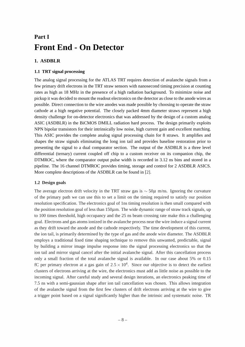
The differential signal from the shaper is AC-coupled through 8 pF capacitors into the baselinerestorer (BLR) where a bridge diode network with dynamic current control (Figure3) provides avariable impedance shunt across the AC coupled differential signal. Current in the bridge deter-mines the shunt impedance and is dependent on the polarity of the differential output. The shuntimpedance increases as signals of the desired polarity are passed to the next stage (discriminator),and decreases when the shaper output returns to baseline. Overshoot (due to discharge of the cou-pling capacitors) is sensed and results in an increase in current in the bridge, lowering its shuntimpedance across the outputs and quickly returns the signal to baseline.
1.3.4 High and low level discriminator
The BLR is followed by two independent discriminators, one with a low threshold level for track-ing, the other with a higher threshold for transition radiation (TR) detection. The low level dis-criminator contains additional integrations to increase the 5 nsec peaking time of the shaper outputto 7.5 nsec and can reliably be set to trigger on signals between 1 and 10 fC. The low level dis-criminator is designed to mark the time of arrival of the avalanche signal from the earliest primaryelectrons liberated by an ionizing track. Since the primaries move at a predictable velocity the timeinformation can be used to designate the closest point of approach of the track to the wire. The TRdiscriminator utilizes the same basic configuration, but has a 10 : 1 attenuation at its input and adds5 ns to the shaping time to allow integration of the prompt and reflected straw signal for accuratedetection of the Transition Radiation photons.
1.3.5 Ternary driver
The low level and TR discriminators switch separate 200µA currents between shared differentialoutputs to form a current sum of the combined discriminator outputs. This simple encoding schemeshown in Table2 is based on the assumption that the track discriminator output is always presentwhen the TR discriminator is triggered due to its lower threshold [2].
– 11 –
Figure 3. Baseline restorer functional schematic.
Signal Detected Ternary Plus Ternary MinusBelow Low and High Threshold -200µA 0 µA
Above Low Threshold -100µA -100µA
Above Low and High Threshold 0 µA -200µA
Table 2. ASDBLR Single Channel Ternary Encoded output
1.4 Wafer fabrication
The ASDBLR was fabricated in a 0.8µm minimum feature size, BiCMOS Silicon On Insulator(SOI) process. Two prototyping cycles allowed us to understand issues of yield and substratepickup that were not apparent from manufacturer provided information. Our previous experiencewith several generations of similar analog wire chamber ASICS led us to expect a yield of 90%or greater. We were somewhat surprised to find that our yield was closer to 65% after folding inreasonable parametric limits on threshold. Measurement of test resistors on the fabricated wafersshowed an unusually large number of devices whose absolute resistance varied by 20% or largerfrom the average value on the wafer. We attributed this to a high defect density in the process.Although there was not an obvious circuit based way to eliminate this quality control problem wedid adjust the number of wafers purchased to accomodate this relatively consistent low yield.
A second problem had to do with pickup between circuit blocks. Analog device models pro-vided by the manufacturer did not account for capacitance across the insulator layer to the backsubstrate leading to an observable difference between calculated and measured impulse response
– 12 –
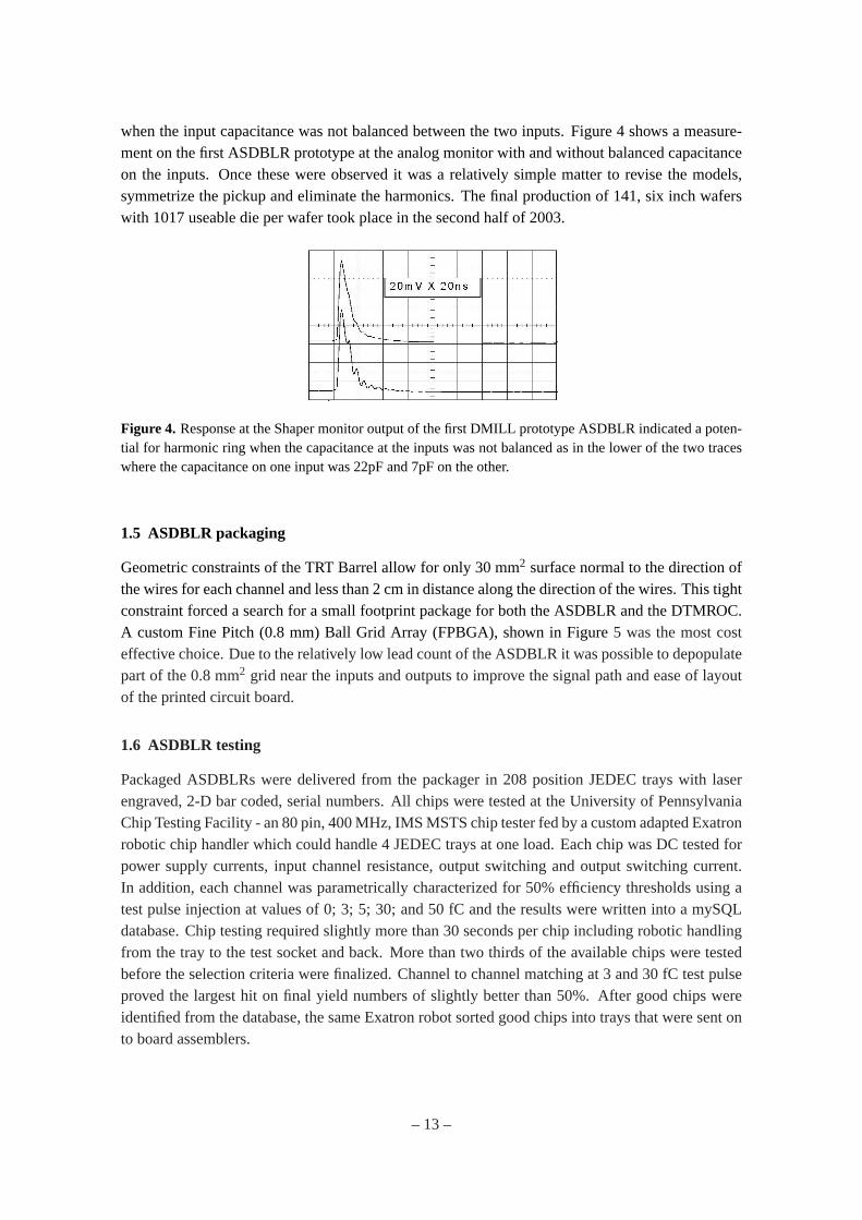
when the input capacitance was not balanced between the two inputs. Figure 4 shows a measure-ment on the first ASDBLR prototype at the analog monitor with and without balanced capacitanceon the inputs. Once these were observed it was a relatively simple matter to revise the models,symmetrize the pickup and eliminate the harmonics. The final production of 141, six inch waferswith 1017 useable die per wafer took place in the second half of 2003.
Figure 4. Response at the Shaper monitor output of the first DMILL prototype ASDBLR indicated a poten-tial for harmonic ring when the capacitance at the inputs was not balanced as in the lower of the two traceswhere the capacitance on one input was 22pF and 7pF on the other.
1.5 ASDBLR packaging
Geometric constraints of the TRT Barrel allow for only 30 mm2 surface normal to the direction ofthe wires for each channel and less than 2 cm in distance along the direction of the wires. This tightconstraint forced a search for a small footprint package for both the ASDBLR and the DTMROC.A custom Fine Pitch (0.8 mm) Ball Grid Array (FPBGA), shown in Figure5 was the most costeffective choice. Due to the relatively low lead count of the ASDBLR it was possible to depopulatepart of the 0.8 mm2 grid near the inputs and outputs to improve the signal path and ease of layoutof the printed circuit board.
1.6 ASDBLR testing
Packaged ASDBLRs were delivered from the packager in 208 position JEDEC trays with laserengraved, 2-D bar coded, serial numbers. All chips were tested at the University of PennsylvaniaChip Testing Facility - an 80 pin, 400 MHz, IMS MSTS chip tester fed by a custom adapted Exatronrobotic chip handler which could handle 4 JEDEC trays at one load. Each chip was DC tested forpower supply currents, input channel resistance, output switching and output switching current.In addition, each channel was parametrically characterized for 50% efficiency thresholds using atest pulse injection at values of 0; 3; 5; 30; and 50 fC and the results were written into a mySQLdatabase. Chip testing required slightly more than 30 seconds per chip including robotic handlingfrom the tray to the test socket and back. More than two thirds of the available chips were testedbefore the selection criteria were finalized. Channel to channel matching at 3 and 30 fC test pulseproved the largest hit on final yield numbers of slightly better than 50%. After good chips wereidentified from the database, the same Exatron robot sorted good chips into trays that were sent onto board assemblers.
– 13 –

Figure 5. Two ASDBLR and one DTMROC ASIC, in their custom FPGA packages are shown in comparisonwith a US dime for size comparison. The solder balls are 300 micrometers in diameter on an 800 micrometergrid.
1.7 Radiation hardness
The ASDBLR relies on the characteristics of the DMILL NPN transistors, resistors and capacitors.The most sensitive parameter observed to change with radiation is the NPN transistor gain. Figure6shows the gain (Beta) of the DMILL process NPN transistors as a function of current density afterexposure to 3.5×10¹⁴ n/cm2, the calculated accumulated dose after 10 years of ATLAS operationat design luminosity. As indicated in the figure the gain of the input transistor ( 7µ A/m) wasmeasured to be only 23 after exposure. An improvement of a factor of two was observed afterannealing the transistors at> 100oC for 24 hrs, a condition that may better represent the very longterm exposure the front end electronics will experience. See Ref [4] for more information.
Our radiation tests have shown that the ASDBLR is capable of withstanding the predicted3.5× 1014 (1 MeV NIEL - Non Ionizing Energy Loss) neutrons/cm2 and 7 Mrad ionizing radi-ation without substantial performance shifts, although it has also been shown that unexpectedlyhigh levels of thermal neutrons, in addition to the projected higher energy neutron dose, wouldcompromise the useful lifetime of the ASDBLR [4]. The ASDBLR threshold input gives accessto an on-chip transistor and, thus, a way to obtain a sensitive measurement of the change in npntransistor gain after radiation damage. The ASDBLR threshold input goes directly to the base ofa 4 µm npn transistor in each of the 8 channels. As shown in Figure7 knowing the current in thebase and collector of those transistors allows calculation of the current gain where Beta = Collectorcurrent/Base current.
– 14 –

Figure 6. Measured DMILL SOI transtor current gain as a function of current density. The arrows indicateapproximate collector current densities in various parts of the ASDBLR circuit.
The DMILL NPN transistors in the ASDBLR show very little sensitivity to ionizing radiationat the doses expected after 10 years of operation at LHC. Figure8 Shows the channel by channelthreshold offsets before and after exposure to 7 Mrad of Co60.
– 15 –

Figure 7. Measured change in ASDBLR threshold current versus DTMROC DAC setting (one DAC count= 5mV) after exposure to 3.5×10¹⁴ n/cm2 1 MeV NIEL neutrons at the French Prospero facility. Usingthe measured threshold current the worst case transistor gain was estimated to be 55 after exposure. Thesedevices were annealed prior to measurement.
Figure 8. The plot above shows the measured ASDBLR threshold offsets before and after exposure to 7Mrad of Gamma radiation. A small amount of broadening is evident in the distribution plotted with the solidline.
– 16 –
2. DTMROC
2.1 Introduction
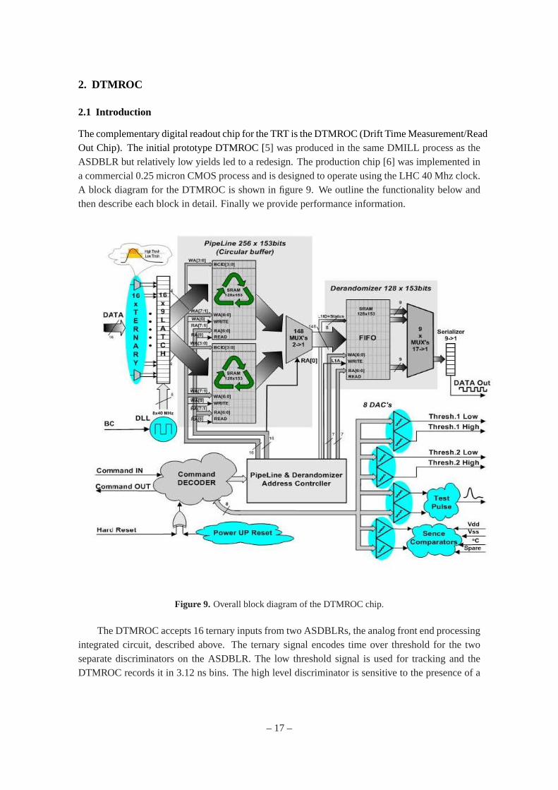
The complementary digital readout chip for the TRT is the DTMROC (Drift Time Measurement/ReadOut Chip). The initial prototype DTMROC [5] was produced in the same DMILL process as theASDBLR but relatively low yields led to a redesign. The production chip [6] was implemented ina commercial 0.25 micron CMOS process and is designed to operate using the LHC 40 Mhz clock.A block diagram for the DTMROC is shown in figure9. We outline the functionality below andthen describe each block in detail. Finally we provide performance information.
Figure 9. Overall block diagram of the DTMROC chip.
The DTMROC accepts 16 ternary inputs from two ASDBLRs, the analog front end processingintegrated circuit, described above. The ternary signal encodes time over threshold for the twoseparate discriminators on the ASDBLR. The low threshold signal is used for tracking and theDTMROC records it in 3.12 ns bins. The high level discriminator is sensitive to the presence of a
– 17 –
transition radiation signal and that output is latched as a single bit during each 25 ns clock cyclethat it is active.
The DTMROC has five differential LVDS connections to the back end electronics – the 40MHz clock (BX), Reset and Command In provide timing, reset and control input functionalitywhile Data Out and Command Out provide readout of the drift time data dn the control data re-spectively. BX, Reset, Command In, and Command Out are bussed to a group of DTMROC chips.Each DTMROC has a private Data Out line to the back end electronics.
The DTMROC contains a programmable depth Level 1 pipeline to hold the front end datauntil the first level trigger arrives. When a trigger arrives as a serial string on the Command In line,the data (eight bits from the digitization of the low threshold input and a single bit from the stateof high threshold input) for three successive bunch crossings are transferred to a derandomizingbuffer. From the derandomizing buffer the data are serialized and sent off chip over a low voltagedifferential signal (LVDS) twisted pair copper connection – Data Out. The data are preceded by aheader giving the contents of a 3 bit trigger counter and a 4 bit clock counter. There is also a bitto indicate if the chip is in “sendid mode,” in which case it sends its hardware address rather thanthe input data and a bit to indicate if any one of a number of error conditions is true – a total of 10header bits.
In addition to the main data path described above, the DTMROC Command Out port is used forreading back the contents of downloaded registers and of status registers. In addition, the CommandOut port implements, an optional asynchronous wire-or output of the 16 low level outputs of ternaryreceivers for use in self triggered running.
The DTMROC also contains four 8 bit Digital to Analog Converters (DACs) to set the low andhigh thresholds on each of the two ASDBLRs to which the DTMROC is connected. There are alsoa pair of one bit digital outputs that are used to control the shaper of the ASDBLR.
A testpulse generator with programmable amplitude and timing is provided for testing andcalibrating the ASDBLR. Four additional DACs and four comparators are available to measurethe temperature and Vdd (+2.5V) on the DTMROC die as well as Vcc (+3V) and Vee (-3V) forthe ASDBLR via two external connections. This array of DACs and comparators is refered to asVT-sense (Voltage/Tempature-Sense).
A Command Decoder provides register read and write functionality and well as general chipcontrol and fast signal decoding. The Command Decoder receives commands over the CommandIn line and transmits readback data over the Command Out line.
2.2 Analog blocks
2.2.1 Ternary receiver
The ASDBLR output is a constant-total-current, differential ternary signal (0, 1, and 2 | 2, 1, and 0units) where a signal unit is 200 +100 / -40µA. This current is pulled from the DTMROC TernaryReceiver inputs which sit at about +1.2 V and have an input impedance of about 200 Ohms. In thisscheme, there is a constant return current flow through the negative ASDBLR supply to the analogand then digital grounds and then the positive DTMROC supply. This non-zero return currentproduces a small DC offset between analog and digital grounds but obviates the need for a muchmore complex fully balanced output drive stage in the ASDBLR.
– 18 –
Table2.2.1gives the encoding function of the current.
Amplified Signal in the ASDBLR True Signal Complementary Signal
No signal above thresholds 2U 0Signal between low and high thresholds 1U 1USignal above both thresholds 0 2U
Table 3. Encoding function of the current in units “U” of current that are sourced from the DTMROC inputsinto the ASDBLR outputs.
The ternary receivers convert the encoded currents back into two separate digital waveforms.Under quiescent conditions (no ASDBLR pulse) there is 400µA leaving a TRUE input of theDTMROC. A pulse will be viewed as a rising voltage on the TRUE input.
The Ternary Receiver circuit is capable of accurately decoding tri-level differential currentpulses as short as 4ns long (at base). The circuit is based on differently ratioed differential currentmirrors after the common gate current receiver. The use of ternary signals permits high-densitycommunication between the ASDBLR and DTMROC chips without driving up pin-counts andwithout causing self-oscillations via large signal couplings back to amplifier inputs.
2.2.2 LVDS interface
The interfaces to the back end electronics are all implemented as true LVDS differential signals.The BX, Reset and Command In input lines are received in standard high impedance differentialreceivers taken directly from the RAL library with a guaranteed sensitivity for signals of 25 mVdifferential or greater and minimum signal widths of about 5 ns.
The Data Out driver is a custom design based on standard LVDS topology with dual currentsources driving an H bridge output. For the DTMROC Command Out driver to function on a multi-source Command Out bus it was necessary to include a tri-state function to turn off the currentsources except when a particular chip was addressed. Given the need for the tri-state functionality,it was straightforward to include a secondary mode of operation for the Command Out driver whereit can be used as a simple current drive into a distant summing node. By connecting the input of theCommmand Out driver to an OR of the 16 straw tracking signals, it is possible to treat the set ofCommand Outs on a given front end board as a single current sum so that a distant comparator canact as a multiplicity trigger on any minimum number of simultaneous ternary inputs. This allowsself triggering for cosmic or source running and was used during some of the commissioning tests.
2.2.3 Digital to analog converters
Four dual, eight-bit Digital to Analog Converter (DAC) blocks are used in the DTMROC to providea total of four ASDBLR thresholds, two temperature – voltage monitor reference voltages and twoTest Pulse Output References. Each dual DAC creates two 8 bit reference voltages with a sourceimpedance of 5 kOhms. Two 8 bit switch arrays steer ratioed currents from current mirror slavedevices to provide an 8 bit current output into an internal 5 kOhm resistor. Current in the mirrormaster array is adjusted by an Opamp driver to provide an output voltage across an internal resistor
– 19 –

( 10 kOhm) that matches the internal band gapŠs 1.25 V reference. The output of each DAC is avoltage in the range of 0 to 1.25 V with a least significant bit step of about 5 mV.
Two of the dual DACs are used to program thresholds for the ASDBLR chips associated withthe DTMROC – two tracking thresholds and two transition radiation thresholds. The remainingtwo dual DACs are used to control test pulse amplitudes and measure on-chip temperature andvoltage and two external voltages as explained in the next sections.
2.2.4 Testpulse generation
Each ASDBLR has two test inputs to couple an external test signal to an on-chip bus capacitivelyconnected to each of four even or four odd ASDBLR preamp inputs. The DTMROC has a testpulse generator that provides a shaped signal to these ASDBLR test inputs. The DTMROC testsignal is shaped as an integral of the expected point ionization signal in a TRT straw so that thedifferentiated signal at the ASDBLR preamp input closely follows the shape of a pulse from a Xefilled 4 mm straw.
Each test pulse generator is adjustable in amplitude (roughly 0 to 50 fC) and time (roughly 0to 35 ns relative to the BX clock). A dual 8 bit DAC (see above) controls the amplitude of the Oddand Even test pulse outputs although only the top six bits of the DACs are connected to the controlregister. An external connection (TPbias) can be used to adjust the output range – the nominal 0-50fC range requires a 9 kOhm resistor between TPbias and 0V. The time delay of both Odd and Evenoutputs is controlled relative to BX through a single 32 position delay line, addressable via a fivebit register field. There are separate enable bits for the Odd and Even test pulse outputs to simplifyprogram control of the various test pulse sequences.
2.2.5 Temperature and voltage sense
A simple measuring scheme is used to monitor on-chip temperature, Vdd voltage, and two off chipsense inputs. A monitored voltage is compared to a programmed DAC value by a dual low offsetvoltage comparator. The comparator output value is stored in the Common Status Register and canbe enabled as an input to the Error Bit. The DAC voltage range is limited to 1.25 V so the powersupply voltages are scaled down suitably.
Two on-chip comparators are fed from one DAC output. These two comparators are attachedto an external input via an on-chip or an external divider and to an internal current source feedinga temperature sensing diode. Two additional comparators are fed from the a second DAC andcompare that value to a second external voltage source and an internally divided copy of Vdd.
By sweeping the DAC setpoints it is possible to find the value of Vdd with a resolution ofabout 10 mV or the temperature with a resolution of about 2 degrees C given the 5 mV LSB ofthe DACs. By attaching the external voltage inputs of some DTMROCs on a board to the localASDBLR Vcc or Vee power lines it is possible to monitor power supply and temperature valuesat each front end board. Because the comparator outputs can be set as an input to the error bit, byproperly enabling the error flags it is possible to learn of significant power or temperature changesin a few tens of microseconds.
– 20 –

2.3 Timing
2.3.1 DLL
The Delay Locked Loop (DLL) used in the DTMROC is a standard design with eight delay stagesmade with current starved inverters feeding back via the last inverter to a common point wherethere is a comparison with the incoming 40 MHz LHC clock. The power rail for the starvedinverters is then adjusted up or down depending upon the sign and magnitude of the phase errorat the comparison point. This gives eight buffered clocks, BX0 to BX7 which are used to latchincoming straw data in 3.12 ns bins.
The DLL naturally produces a nearly perfect 50% duty cycle clock waveform and this may,under register control, be used as the clock signal throughout the DTMROC upon register selection.This, however, does not obviate the need for a stable 40 MHz external clock, it simply relaxes theduty cycle requirement on that clock.
As a diagnostic and monitoring tool, the DTMROC includes an eight bit latch for the BX0..BX7signals that is updated each LHC clock cycle. A latch pattern showing a 50±12.5% duty cycleresults in a “DLL locked” bit set in the Common Status Register.
The DLL can be reset via the command decoder or via the external Reset line or upon powerup.
2.3.2 Latch
The asynchronous data from the ASDBLR ranges in duration from∼5 ns to many 25 ns clockcycles. For the low threshold (tracking) signal, the asynchronous data can simply be latched con-tinuosly by the BX0..BX7 clocks producing an ongoing bit stream record with 3.12 ns resolution orabout 1 ns RMS. Each clock cycle (eight 3.2125 bins) is then recorded as an eight bit record in theLevel 1 Pipeline memory. However, the high level threshold, because it only needs to be recordedas one bit per clock cycle, requires a synchronizing latch sensitive to transitions as short as 5 ns.Any high state during a given clock cycle is then stored in the Level 1 Pipeline as a high for thenext clock cycle. In addition, a special “accumulate” mode has been implemented for this latch sothat it does not reset each BX cycle as it would in normal data taking, but resets only upon externalcommand. This is useful for chamber testing with radioactive sources or looking at average noiserates.
2.4 Digital blocks
2.4.1 Pipeline
The Level 1 Pipeline is a logical FIFO block that stores the 9 bits (1 high threshold bit plus 8 timedigitization bits of the low threshold) of latched data from each input channel, the current value ofa 4 bit clock counter plus a 1 bit error flag from the DLL. This FIFO is designed to hold the frontend data for the length of the Level 1 trigger latency.
The pipeline is implemented as two banks of 128 deep by 153 bit wide Random Access Mem-ory (RAM) build out of 34 blocks of 128x9 bit memories. It operates as a continuously runningcircular buffer, updating the read and write pointers into the memory. Writes (and therefore reads)alternate between the two banks of RAM to minimize power consumption fluctuations that couldoccur on parallel access to all memory blocks.
– 21 –

2.4.2 Drandomizer
The Derandomizer is an additional buffer also acting as a FIFO built from the same synchronousdual-port static RAM memory as the Pipeline, but with half the number of banks giving a storagecapacity of 128 words of 153 bits. Upon receipt of a L1A the current Pipeline output word andthe following two consecutive words are stored in the Derandomizer for readout. In addition tothese data, the SENDID status bit, the L1ID and the Common Error status bit are stored. This gives441 bits1 to be stored per event. The Derandomizer can store 42 events. In the case of memoryoverflow control logic provides a “full” flag and skips complete events avoiding synchronisationproblems until the memory clears an event and is able to store a subsequent event. The Deran-domizer and Pipeline SRAM blocks are equipped with Build-In-Self-Test (BIST) controlled viathe Configuration register. The BIST result can be read out from the General Status register.
2.4.3 Serializer
As soon as the Derandomizer is not empty data is placed serially on the DataOut line at a 40MHzbit rate. As the event size is constant a simple protocol is used with a 3 bit preamble S101T sent atthe beginning of each event. When idle, the data output signal is S0T.
2.4.4 Command decoder
The command decoder block receives LVDS BX and a CommandIn signals from the TTC. Thecommand decoder examines the CommandIn stream bit by bit and issues all the necessary timingsignals (L1A,...), internal registers read/write strobes and data. As implemented the decoding al-gorithm is very simple and is built from a shift register, a look-up table with valid command codesand comparator logic. This architecture is, in this case, lower cost in power and resources thana finite state machine. In order to insure that the circuit is robust against single event upset addi-tional logic was incorporated. The decoder for the critical ‘fast’ commands (L1A, SoftReset andBunchCrossingReset) was triplicated for error correction as was the command length counter. ASsurveillanceT counter was implemented to guarantee the RTL state coverage and to release anyaccess lasting longer then 171 clock cycles. Upon a read request the command decoder seriallytransmits the contents of the selected register on the differential CommzandOut line, three clockcycles after the last bit of the command,. This CommandOut line is common to multiple chips ona board and therefore has a ‘tri-state’ capability. A three bit preamble (‘101’) is used for each datatransmission and the idle state of this line is S ‘HiZ’. The chip address is defined by setting externalpins.
2.4.5 Error handling
The implemented protocol is based on the ABCD chip specification, which lacks any advancedprotection against transmission errors. The bit patterns are however chosen such that a single biterror should not cause the acceptance of a wrong command. An erroneous bit pattern in the middleof a commmand causes a flush of that unrecognized field and an attempt to decode the followingcommand.
– 22 –

Figure 10. DTMROCŠs time-measuring performance with the nominal 2.5 V and 2.0 V power supply. A4.0 ns wide tracking pulse was injected at 100 ps intervals across three full clock periods, 75 ns in total.The picture shows the leading (red) and falling (blue) edges fit deviations and differential non-linearity assampled by a single chip channels.
2.5 Measured performance
The preproduction fabrication of the design was fully successful and so the full production run of48 wafers was done using the original masks which included lithography adjustments to simulatetwo “faster” and two “slower” (from 85% to 125% of nominal propagation time) variations aboutnominal process parameters. The DTMROC preproduction tests looked at logical performance,time linearity, DAC linearity, and performance over voltage and process variations. As shown inFigure10, the time linearity is at the expected 1 ns level, differential and integral, not only at thenominal 2.5 V Vdd but down to at least 2.0 V. The basic logic of the chip such as the commanddecoder, was shown to work properly at over 100 MHz at 2.0V, but the RAM blocks did show somedegradation at elevated clock speeds, lowered process speed and lowered supply voltage as shownin Figure11. As noted above, the RAM blocks are tested with a built in self test routine as accessthrough the DTMROC command structure is indirect and full coverage tests would be very timeconsuming.
Production tests of the chips, conducted at the University of Pennsylvania Integrated CircuitTest Facility concentrated on checkingIDD, exercising the built in memory self test, and then load-ing preset pulse patterns into the sixteen input channels and verifying proper time encoding withinone LSB. The ternary receivers were checked for proper perfomance over their full range of am-plitude and offset as were the LVDS I/O blocks. The DAC outputs and VT sense DACs were alsoexercised over their range and the test pulse output was checked at several values of amplitudeand time delay. About 40,000 test vectors per chip were completed in about 30 seconds including
– 23 –

Figure 11. RAM access rate vs. Vdd and for various process variations. Note that for DTMROC productionrun, the slowest (125% on this plot) process variation was not packaged.
robotic handling. All production chips were laser engraved with 2-D barcode serial numbers andtest results were stored in a database. Chips passing all test criteria (about 85% yield) were pulledfrom the JEDEC trays and placed into final trays for the assembler by the same robot.
– 24 –

3. Board designs
3.1 Introduction
Design of the front end boards, the detector grounding and shielding, and the power and signalconnections to the outside world must be implemented very carefully to achieve optimal perfor-mance. For instance, the 30 to 70 cm long straw tubes in the TRT are within a small factor of beingideal 1/4 wave antennas tuned to the ASDBLR peak bandwidth of about 33 MHz. In addition, theASDBLR inputs must be carefully isolated from the 40 MHz digital logic of the DTMROC,
The geometry and other constraints of the TRT End Cap [7] and Barrel [8] are very differentso the designs of the End Cap and Barrel printed circuit boards need different optimizations. Thebasic schematic is, however, the same in each case – input protection (24Ω series resistor witha diode clamp to ground) at the detector and then ASDBLR, DTMROC, and power filtering onthe front end boards. All signals in the system are differential except that the straw anode inputis only matched pseudo-differentially by a trace carrying the ASDBLR dummy input as close tothe detector as possible. The End Cap and Barrel printed circuit designs and justifications for theoptimizations are discussed in detail below.
3.2 End cap boards
The End Cap straws are positioned radially and so while the straws nearly touch with a center tocenter distance of 5.2 mm on the inner radius of the TRT, the straw to straw center distance alongtheφ direction is 8.2 mm at the outer radius where the electronics are located. This allows almost3/4 of a cm2 per channel for the electronics located on the tread of the End Cap wheels. Thislocation for the electronics, at the outer radius of the TRT up against the ATLAS solenoid cryostat,means that the radiation length of the electronics package is not as critical a concern as it is in theBarrel case where the electronics must be located at the end of the Barrel just before the End Cap.There is also, by design, sufficient room inr to allow separate, albeit close packed, layers of printedcircuit to handle the analog (ASDBLR) and digital (DTMROC) parts of the system.
3.2.1 ASDBLR boards
There are two schematically identical but physically different designs for the ASDBLR boardsshown in Figure12 for the Type A and Type B End Cap Wheels since the Type B wheels areconstructed with half the straw density in the Z direction. The Type A boards are about 60 mmsquare and serve 64 channels of detector (1/96 of a wheel inφ ) with eight ASDBLR chips. TheType B boards are about 120 mm in the Z direction to match the wheels. Both types are fourlayer, 1.5 mm thick, through-via designs. Connection to the straw anodes and cathodes is madevia miniature connectors to the End Cap WheelWEBs, complex rigid flex printed circuits thatserve to attach the electronics boards to the detector both physically and electrically [7]. The highvoltage decoupling capacitors for the cathode connections and 24 Ohm input protection resistorsare mounted on the WEB as are the HV protection fuses which also serve as blocking or isolatingresistors to the HV supply.
ASDBLR ternary outputs are sent to the DTMROC chips mounted on the Triplet Boards viafour high compliance miniature connectors. ASDBLR control signals from the DTMROC andpower for the ASDBLR chips also travel over these four connectors.
– 25 –

Figure 12. A Wheel (l) and B Wheel (r) ASDBLR boards top view showing the ASDBLR chips and thefour multi-pin white connectors going to the Triplet Board. The semi-circular cutouts in the board edges aredesigned to clear plumbing and HV connections to the wheels.
3.2.2 DTMROC triplet boards
The Triplet boards are identical for Type A and Type B wheels. One Triplet board serves threeASDBLR boards – 32 Triplet boards per End Cap Wheel. Each triplet board, shown in Figure13,has 12 DTMROC chips and is constructed as three separate four-layer through-via printed circuitsjoined by flexible jumpers. The jumpers allow flexibility so that the Triplet can follow the curveof the End Cap Wheels. An initial design effort using rigid flex technology demonstrated goodperformance, but was abandoned because of cost considerations and because the stiffness of theflex circuitry was too great to allow easy assembly on the wheels.
3.2.3 Shielding
For the TRT End Cap, the Faraday shield around the straws is completed through the WEB structureon one side of the wheel up through the ASDBLR board and down the opposite WEB as shown inFigure14. The analog ground plane of the ASDBLR board acts not only as the cathode connectionand reference for the ASDBLR input but also as a part of the Faraday shield. As a secondaryshield, it was learned that completing the connection of the digital ground plane of the Tripletboards with a low impedance phosphor bronze clip between the edge plated segments of the Tripletboards provided additional cross talk protection from the digital logic on the Triplet. A full externalFaraday shield constructed at the level of the TRT cable trays surrounds the detector and electronics.
3.2.4 Power distribution
Power is brought to the Triplet via the same 60 pin connector that also carries the four controllines and the 12 data output lines. The +2.5V power for the DTMROCs is filtered at the 60 pin
– 26 –

Figure 13. End Cap Triplet board showing the four DTMROC chips per segment with the power and dataconnector on the right. The four white jumpers between segments carry control and data signals and powerand power returns. Note that the breakaway bars at top and bottom of the triplet are removed after testing.
Figure 14. Cross-section drawing of the End Cap construction. The DTMROC Triplet board is at the verytop, then the ASDBLR board, the cooling structure and the WEBs.
connector, is returned via the digital ground plane on the triplet board, and is distributed only onthe Triplet board. The±3V power for the ASDBLRs is filtered to the analog return at the 60 pinconnector and then distributed to the three ASDBLR boards. Analog and Digital power returns arecommoned at the connector. Cooling is described in section4.2.
3.3 Barrel boards
The Barrel readout system must function in a much more constrained space and, in addition, there
– 27 –

is a stringent radiation length limit as the boards must be situated in the middle of a trackingregion. The board area per straw is also about a factor of two less than in the End Cap case. Themounting of the Barrel modules in the Barrel Support Structure (BSS) defines a set of triangularspaces shown in Figure15 into which the electronics must fit in order to connect to the anode andcathodes brought out on the module tension plates.
Figure 15. End-on view of the TRT Barrel during above ground testing at CERN before installation in theATLAS detector hall. Each of the three types of modules (1,2, and 3) is bisected by a member from theBarrel Support Structure. These six different triangluar shapes define the geometry of the front end boards.
After exploring a number of possible design concepts that failed to meet all the design con-straints, the collaboration settled on a single board mounting both ASDBLR and DTMROC chips [9]as opposed to the two board solution used in the End Cap.
3.3.1 Design constraints
The connectors designed into the Barrel Tension Plates (individual sockets for 0.5 mm pins ar-ranged in groups of 16 anodes and 6 grounds) shown in Figure16 [8] are not suitable for simul-taneous mass insertion as would be required by a triangular printed circuit board serving from 10to 27 of these 16 anode patterns. In addition, the areal electronics density required, especially inthe smallest (Type 1) modules, is somewhat greater than practical. Therefore, an additional smallboard, the Protection Board, was added to the scheme to allow a transition from the 0.5 mm pin
– 28 –

connectors to the high compliance miniature connectors used on the End Cap – this improves themechanical compliance to allow, in the worst case, making 600 simultaneous connections and pro-vides a small additional surface area to house the clamp diodes and input protection resistors forthe ASDBLR inputs.
Figure 16. Crosssectional view of a barrel module tension and HV plate region. The Protection Board(labeled ‘Electronics Card’) is shown plugged into sockets in the tension plate. The active electronics plugsinto and is parallel to the Protection Board.
Given the necessity of a Protection Board and given that the overall depth in Z available forBarrel electronics including cooling and connectors is about 1.5 cm, a single substrate printedcircuit solution becomes almost inevitable. Because of the obvious mechanical difficulties in usinga liquid cooled plate under the ASDBLRs, a set of two piece machined Al plates were designedto be attached to the outer or DTMROC side of the triangle boards – in that way the coolingconnections could inhabit space reserved for other plumbing connections.
3.3.2 Design rules
Although variations in geometry by end and by module layer require a total of 12 different boardand cooling plate footprints, the design approach is the same for each. The basic rule is to separatethe board into analog and digital domains splitting a total of 14 layers equally between them. Fourlevels of blind vias allow isolation of analog and digital signals within their separate domains. Allfast signals are low level differential. Barrel boards are arranged in 16 channel ASIC triplets con-sisting of two eight channel ASDBLRŠs and one DTMROC. Analog connectors and ASDBLRŠsface inwards towards the barrel module. Two signal layers separated by an analog ground planeutilize short vias to isolate the inputs from the rest of the board. An empty layer below the inputsignal layers and a power layer with cutouts corresponding to the location of input signals min-imize the capacitance to the other board layers. The analog side is enclosed by a second analogground plane with a power layer finally facing outwards towards the digital side. The layer stackupis shown in Figure17
– 29 –

Figure 17. Cross-section of the printed circuit planes showing the digital and analog domains within the14 layer stackup. Four different classes of blind vias, two for the digital and two for the analog domain areused for almost all connections except direct connections for ASDBLR outputs to the DTMROC and controlsignals from the DTMROC. Power is provided from a through-hole connector. The edge plating noted onthe left of the figure wipes the RF fingers on the Barrel Support Structure (BSS).
The DTMROC ASICS are placed on the outermost layer away from the barrel. Analog anddigital grounds are completely separate but provision is made on the digital side to connect themusing surface mount resistors placed around the perimeter of the triangular footprint. At theselocations direct access to analog and digital ground is provided with large pads to allow low induc-tance connection from digital to analog ground and from analog ground to the conductive supportstructure of the barrel module. The support frame of the barrel module, the RF contacts (“fingers”)around the perimeter of each board, the analog layers of the board, and the inner and outer cylindersof the Barrel comprise a Faraday shield which surrounds the “analog zone” of the detector – thestraws and the signal paths to the inputs of the ASDBLR. Special care is taken at the two sides ofeach module where HV connections to the cathodes are made via wide Kapton foils – the foils arenotched every few centimeters and custom grounding clips bridge the gap between the RF fingerson the BSS and the edge plated analog board ground.
3.3.3 Barrel printed circuit boards
The 12 final designs of the boards shown in Figure18 are designated ARxyz (where AR is an his-toric reference to anActiveRoof), x is the module number (1-3), y isFront orBack correspondingto C or A sides of ATLAS, and z isLarge orSmall triangle of the pair (the smaller triangle has itsbase at smallerR. Front and Back boards are not mirror images of each other as the Tension Platedesigns reflect a translation, not a mirror operation from end to end in the modules – this forcestwelve distinct printed circuit designs. General characteristics of these designs are listed in Table4.
– 30 –

Board No. DTMROCs No. Clk Groups No. Power Connects
AR1F(B)S 10 1 1
AR1F(B)L 11 1 1
AR2F(B)S 15 1 1
AR2F(B)L 18 2 1
AR3F(B)S 23 2 2
AR3F(B)L 27 2 2
Table 4. AR Board Designs
Figure 18. The photograph above shows a module 3 barrel board (two power and Clock Groups) with onethrough hole and one pig-tailed power connector and two data connectors. The DTMROC FBGA chips canbe seen on the top of this board.
3.3.4 Power distribution
While the End Cap uses a single connector for power and data, that connector is much too largefor use in the Barrel case. All AR boards have separate power and data connectors. The dataconnectors are 60 pin surface mount versions of the high compliance connectors used to connectto the Protection Boards and the power connectors are 6 pin industrial style through hole connec-tors. As seen in Figure18 some of the power connections were implemented as pig-tails to easerouting of the power connections through the plumbing. Unlike the End Cap case where electricalconnections were made to the boards before plumbing connections and shielding were completed,the Barrel cabling was installed after the full plumbing manifold system was in place. Cooling is
– 31 –

described in section4.2
3.4 Testing program
All TRT front end boards were assembled by industrial printed circuit assemblers and then shippedto Neils Bohr Institute for visual inspection, burn in and testing. Each board was run on a currentand voltage monitored stand at elevated temperature for one week or more prior to detailed testing.Boards failing the initial tests were repaired either at NBI or sent to the University of Pennsylvaniafor diagnosis and repair. Tested boards were then sent to CERN, retested in the surface assem-bly building, mounted on the detector, and then tested again. Results of the on-detector tests arecovered in section14.2.
– 32 –

4. Cabling and cooling
4.1 Cabling
The organization of the cabling in the inner detector of a collider experiment (the innermost partof the tracking system) is always a logistical and engineering struggle for compromise betweenlow mass and minimal volume versus high quality signal and services transmission. The followingparagraphs describe briefly the solutions deployed.
The cabling of the TRT has been split into two separate parts in the two different regions of thedetector – Front End to Patch Panel (Type II cables in ATLAS nomencalture) and then Patch Panelto USA15 (Type III cables) [10]. The regions differ in their environmental design constraints. Thedetector contains the following types of cable:
• Signal cables serving for the data transmission, read-out, timing and temperature sensing.
• High Voltage cables to bias the detecting elements
• Low voltage power cables to supply the FE electronics and auxiliary electronics on PatchPanels
• Control cables for several functions exercised on the Patch Panels
4.1.1 Detector to patch panels
For the innermost part – Front End to Patch Panel – the main design constraints are mass and vol-ume. The connection between the Front-End electronics on the detector and the Patch Panels routesall the services and data through the very limited space between the TRT and the cryostat wall – aregion shared in phi with the SCT Silicon Tracker services. These ‘Type II’ cables terminate at theTRT Patch Panels (see section5). TheSType IIŠ cables were produced as prefabricated bundlescustomized for each part of the detector. For each function, the cable was chosen for minimumpossible diameterU usually governed by the insulator thickness. For power cables high qualityKapton (polyimide) insulation was a primary choice. There are three types of cables used in thissection of cabling:
• Read-out, control, monitoring (temperature) cablesU individually shielded twisted pairs, tinplated copper conductor, 0.13 mm conductor diameter (36AWG), 4 drain wires Ag platedcopper, wrapped aluminum polyester foil as shield, 0.95 mm overall diameter.
• miniature HV cables – 2 kV mini-coaxial cable, 0.16 mm conductor diameter, tin platedAg/Cu alloy, Aluminum/Polyester foil (shield), 2 drain wires Ag plated copper.
• low voltage shielded cables procured in triplets or doublets according to the voltage setscarried on them.
– Analog – wheel type A – 3 conductors 1.0 mm2, extra flexible tinned copper insulated inMULRAD, 0.12 mm tinned copper braid with a 85 % min coverage, kapton insulated,OD 4.6±0.3 mm
– 33 –

– Analog – wheel type B and barrel – 3 conductors 0.6 mm2 (37 strands of 0.15 mm),extra flexible tinned copper insulated in MULRAD, 0.12 mm tinned copper braid witha 85 % min coverage, kapton insulated, OD 4.00±0.2 mm
– Digital – 2 conductors 1.0 mm2, extra flexible tinned copper insulated in MULRAD,0.12 mm tinned copper braid with a 85 % min coverage, kapton insulated, OD 4.3±0.2 mm
In both the end cap and barrel cases, the HV cables were fabricated as separate bundles foreachφ sector of the detector. For the end cap, low voltage power cables are bundled at the detectorend with the data and control twisted pairs since a common connector is used for both types ofconnections(as shown in Figure19). However, in the barrel case, the low voltage and data-controllines are bundled separately. The data and control lines are such a fine gauge that connection hadto be made via hand soldering in all cases – about 360,000 manual soldering operations. At thedetector side the data and control twisted pairs go to a common connector, but at the Patch Panel endthe data cables go to Data Patch Panels while the control lines go to the TTC Patch Panels. Thus thebundles, even if of only one type of wire, are of a fairly complex one connector to two connectorsform. For the Type II cables, there are 736 complex harnesses (some 2,800 separate bundles ofdifferent types of wire, multiple connectors, and multiple lengths). The LV cables for the barrelused crimped and soldered connections at each end, the End Cap LV cables were soldered to anadapter board on the detector end but used the same crimp connectionsas the barrel power cableson the Patch Panel end. HV cables used commercial crimped multi-way connectors at the PatchPanel ends and were soldered and custom strain relieved into three way commercial connectors atthe end cap or into custom fuse boxes at the barrel end.
Figure 19. Partially assembled End Cap showing two full cable trays at the top and one empty cable tray atthe bottom. Each tray carries cables for 1/32nd of the detector and acts as part of the outer Faraday cage ofthe detector. The blue cables are the 36 AWG data and control shielded twisted pairs, the heavier orange-brown cables are low-voltage supply cables. The light colored HV cables are just barely visible in the uppertray on the left. In this view the triplet boards serving the A type Wheel nearest the interaction point are onthe left and the PPF1 connectors are just out of the picture on the right.
All cables were thoroughly tested for continuity and against shorts on custom built cable testjigs at the bundle assembly site. In addition, the HV cables were subjected to HV leakage tests.
– 34 –

Each cable bundle was labeled for its intended position in the detector as cable lengths dependedin detail upon the route from the detector face, across the cryostat flange, and through the tilecalorimeter fingers and first layer of muon chambers to the Patch Panel boxes.
The bundled cabling (of all types for a givenφ section) was placed into cable trays at CERN,retested, and, as an assembly, mounted either on the cryostat wall (barrel part) or on the mechanicalstructure of the detector (endcap part). The barrel cables run in one piece from the detector up tothe patch panel area. The endcap cables have been split at the cryostat flange where the Patch PanelFront 1 (PPF1) has been located, allowing easier and separate installation of two cableSlengthsŠ.On average, the Type II cables are 12 m long.
4.1.2 Patch panels to control room
From the PP2 location on there is enough space to use standard cables for all functions. The datafrom thirty DTMROCs are merged at PP2 into a single 1.2 Gb/s opto-fiber. The temperatures ofthe NTC board level thermistors and RTD detector and manifold mounted sensors are measured onthe TTC patch panel boards and those cables also stop at PP2. Only timing/control cables and bulkHV and LV cables are installed to connect PP2 with control room and the bulk LV power supplieson the HS structure. The average length of these Type III and Type IV cables is around 75 m withlongest 102 m. The PP2 crates (see section5) contain boards where many DCS control and mon-itoring operations are performed. The communication between those cards and the control roomis performed via a standard industrial bus – CAN bus. This adds CAN bus cables to the inventory(NG18P, 9-pair shielded cable, 120 ohm). The PP2 crates also contain the low voltage regulatorsand their control (see section13) and monitoring. TheS‘bulk’Š power lines which deliver LV toPP2 are simple multi-strand copper cables of 35 and 50 mm2. The signals controlling the data patchpanels (where the data signals from the front-end boards are converted from electrical to optical)are carried down via standard Ethernet-style CAT5 shielded cables. The timing (TTC)system usesfollowing cable:
• 25 twisted pairs round shielded/jacketed discrete wire cable, made of 28 AWG tinned strandedcopper core, overall Al/polyester foil and tinned copper braid, halogen free, flame retardant,110 ohm balanced impedance, color coded.
At the PP2 position the HV cables also change their type via a simple passive disconnect.From the PP2 up to the power supplies in the control room following cable is used:
• 3 kV DC, round overall shielded/jacketed 56 discrete coaxial cables, made of 0.12mm2[AWG26] tinned stranded copper core, overall tinned copper braid (shield), halogen free,flame retardant
4.2 Cooling
The heat generated in the Front End and Patch Panel electronics and the heat lost in the LV powercables must be removed from the cryostat and muon system areas in order to keep the TRT and therest of the Inner Detector at reasonable operating temperatures and to avoid local hot spots withinthe muon tracking system that would distort the geometry of that system. The overall ATLASrequirement is that each subsystem within the cavern be thermally neutral. This need for thermal
– 35 –

neutrality implies the need for an efficient cooling system. The space constraints imposed by thedetector geometry dictate a liquid cooling system. A monophase system relying only on the heatcapacity of the fluid has been shown to be sufficient for the needs of the TRT.
4.2.1 Power Dissipation – front end
The design values for the cooling system load are the following: Power dissipation in the front-end electronics∼ 60 mW per channel (40 mWU ASDBLR and 20 mWU DTMROC) or about320 mW/chip for ASDBLR, and 320 mW/chip for the DTMROC. This gives a total Front Endpower dissipation in the range of 25 kW. In addition, power loss in the cables running from the PP2regulators to the Front End is an additional 4 kW.
4.2.2 Power dissipation – patch panels
The PP2 crates contain three LV distributor boards which dissipate about 60 W each per crate. Forsafety reasons the PP2 crates are closed with front/back panels and there is no air convection whichmight remove the heat. Thus it is necessary to remove the heat via liquid cooling. The PP2 LVcabling running from the power supplies on the HS platforms outside the ATLAS detector has beenrouted in between high precision muon chambers which need to be kept at a constant temperature.So this stretch of the LV cables has also to be cooled.
4.2.3 Design and deployment
For all aforementioned tasks the simple monophase cooling system has been chosen. The idea issimply to circulate through properly sub-divided and configured pipe-work a liquid under sufficientpressure and with adequate mass flow which will remove the heat from the cooled elements. Theliquid has to have a number of special propertiesU to be radiation hard i.e. not decompose underionizing radiation or create aggressive compounds which might endanger the integrity of pipingand the liquid and it should be a good insulator, a dielectric. Due to the inaccessibility of thedetector electronics, a limited leak developing during lifetime of experiment must not be allowedto cause collateral damage through leakage currents or short circuits – a requirement that excludeswater, despite its excellent heat capacity. After series of radiation tests a fluorinert,C6F14, has beenselected.
The cooling station of the design shown in Figure20has been constructed with the capacity of70 kW. It supplies four distribution racks where the main flow is manifolded to barrel and endcapdetectors via 34/rack output lines and 50/rack return lines. A similar cooling station providescooling for the PP2 boxes and the Type III and Type IV cables. The system operates at 6 bars witha settable supply liquid temperature 15-17oC. The value of the pressure is high enough to copewith the dynamic drop in the piping as well as the hydrostatic conditions in a big and voluminoussystem. Operating temperature has to be maintained well above the dew point in the experimentalcavern.
The cooling elements in the barrel detector areS‘cooling platesŠ’ made of aluminum thermallyattached to the electronics boards via a thermally conductive RTV adhesive and supplied with liquidmedium via manifolding pipework running over the BSS face. Each 1/32 in Phi of the barrel is aseparate cooling loop.
– 36 –

Figure 20. Block diagram of the monophase cooling system.
The endcaps electronics is cooled via a logically similar solution with a very different me-chanical design. Here a thermally conductive rubber mat is used as thermal connector betweenASDBLR boards and aluminum plates and SS pipes that carry the fluid. There are two coolingloops per end cap wheel each covering 180 degrees in Phi, but with entrance and exit points rotatedin Phi for each Wheel to distribute the cooling inlet and outlet pipes around the end cap supportstructure [7].
At PP2 each board is bolted to a 2 mm thick Al cooling plate with heat transfer conductiverubber between the cooling plate and the high dissipation components. This cooling plate is thenthermally clamped to the PP2 Box top and bottom plates via expansion clamps. The top and bottomplates of the PP2 boxes have embedded Cu tubing carrying the cooling liquid for that Box. At eachPP2 location, the PP2 Boxes are connected to a local input and output manifold.
The cooling of the cables is realized by routing in LV cable bundles along side the return pipescooling the electronics. Cabling between PP2 and periphery of the ATLAS is cooled by a separatenetwork of piping common to several inner detectors. This network is driven by second coolingstation of identical design to TRT front electronics one.
The system has proven, during system tests, capable of keeping all barrel Front End Boardcomponents under 40 degrees and in the end cap case, keeping even the worst case Triplet board
– 37 –

components, cooled only via conduction through the connectors, under 45 degrees.
– 38 –

Part II
Patch Panels
5. Introduction
The TRT (and Pixel) Patch Panels (formally, Patch Panel 2, abbreviated PP2) are located just out-side the first layer of Muon Barrel chambers in 64 different crates (one crate per 1/32 per end) onfive different platforms on both the A and C sides of ATLAS in as shown in Figure21. These lo-cations were chosen as being accessible during a short shutdown but as close to the Inner Detectoras possible in order to reduce dispersion and signal loss in data cables and voltage drop in the lowvoltage power cables. All the TRT electrical services are either repeated or at least disconnectable,in the case of the High Voltage, at these Patch Panels. Treatment of the TTC signals, and DataSignals is described in the sections below – the HV “patch panel” is simply a set of multiconductorconnector pairs located at the Patch Panel location and is not further described.
The TRT Low Voltage DC power is subject to a final level of regulation, control, and moni-toring at the Patch Panels using custom radiation tolerant linear regulators for both the front endelectronics± 3 V and +2.5 V requirements and the PP2 located logic for TTC and ROD. The LowVoltage regulator PP2 boards are described in detail in the Low Voltage power section (13), but itis worth noting that these boards dissipate most of the power at the PP2 location and dominate thecooling requirements of the PP2 crates.
Figure 21. ATLAS Patch Panel 2 locations.
The data and control signals that go between the Front End Boards and Backend Modules are
– 39 –

all received and repeated at the Patch Panel boards. Each PP2 location houses between 5 and 8Patch Panel boxes, each of which contains all the patch panels which are associated with 1/32nd ofone side of the detector. Each box houses 8 Patch Panels in total; three for 1/32nd of one side ofthe barrel (1 power PP, 1 ROD (or “Data”)PP, 1 TTC PP), and 5 for 1/32nd of one endcap (2 power,1 TTC, 2 ROD). All eight boards in one box share common cooling, power and CAN bus.
Because of the differences in readout granularity and cabling between the Barrel and the End-caps, a single patch panel design could not be used for both barrel and end cap parts of the detector.As a result, the Patch Panels have been implemented using a modular design consisting of an activepart which contains all the functionality and a passive part which handles the routing of signals toand from the Front End boards. This avoids the need for two separate designs which would havecomplicated not only the design and production, but also the testing and installation processes. Thespecifics of each board design will be described in the following sections.
6. TRT-TTC patch panels
6.1 Overview and functionality
The primary function of the TTC Patch Panel is to receive and repeat signals between the TTCand the Front End boards. In addition to this, the board also serves the temperature sensors neededfor monitoring the detector. 20 TTC lines, each consisting of one group of Clock, Command In,Command Out, and Reset signals, are handled by this board. The Command In and Command Outsignals are received and repeated directly, with some shaping in the inputs and outputs (discussedbelow). The Clock and Reset signals, on the other hand, arrive once for every 10 lines, and arefanned out on the patch panel to each of the Front End boards. In addition to being fanned out, theClock signal can also be independantly delayed for each line (after the fan-out) in increments of0.5 ns. Finally, the TTC patch panel is responsible for driving temperature read-out of the detectorand front-end boards, which is accomplished by means of an ELMB [11] which is mounted on thepatch panel. These functions will each be discussed in more detail in this section.
6.1.1 I/O compensaton and filtering
All of the signals entering and exiting the TTC patch panel are LVDS traveling over small coppertwisted pair wire. As mentioned in the cabling section, the signals going to and coming from theTTC travel over 60-100 m of 28 AWG copper twisted pair, while the signals going to and comingfrom the front end boards travel over 10-14 m of 36 AWG shielded twisted pair. The shaping thatis applied to each input or output depends on the cable type, as well as the particulars of the signal;these different approaches will be described below.
There are two different filters that are used for signals coming onto the TTC patch panel board.The Command-In and Reset signals coming from the TTC, as well as the command-out signalscoming in from the Front End boards are received with a passive 11 component differential RLCfilter. This filter has been shown to recover good signal performance for signals traveling up to 100meters over 28 AWG twisted pair wire. The BX Clock signals coming from the TTC are receivedwith an active equalization circuit that can be tuned for cable lengths between 60 and 90 metersin steps of 10 meters by moving a simple jumper. This active equalization is implemented with
– 40 –

a commercially available IC and provides a lower jitter and better signal quality than the passivefilters used for the other signals. This step was taken for the clock in particular because a well-shaped, reliable clock edge is imperative to the proper performance of the drift time measurementin this detector.
For the outputs as well, two different approaches are taken. The signals going out over the 36AWG shielded twisted pair wire towards the Front End boards (BX Clock, Reset, Command in)are shaped with a 3 component passive RL pre-compensation to ensure good signal shape whenthey are received on the Front End boards. The signals going out of the TTC patch panel towardsthe TTC (Command Out only) have no pre-compensation, but instead the LVDS drivers have beendoubled (with the second driver capacitively coupled) to provide the extra drive needed to traversethe 100m cables. The compensation in this case is handled on the TTC board itself with an activeequalization similar to the one described above for the Clock on the patch panel.
6.1.2 Clock fine delay
Aside from receiving and repeating signals, the TTC patch panel also houses a few importantfunctionalities for detector control and monitoring. One of these functions is the fine delay of theclock which is supplied to the front end boards. This delay is used to compensate for differencesin cable length, as well as particle flight time, so that the rising edge of the clock is synchronouswith the earliest arrival of particles at every part of the detector. Because the clock is fanned out tothe front-end board on the TTC Patch Panel, the fine delay of the clock has to be implemented atthe patch panel level. This functionality is implemented using the CERN-developed Delay25 chip,which can provide from 0 to 25 ns of delay for any signal in 0.5 ns steps. The Delay25 chip [12]has 5 delay channels and is controlled by an I2C interface. The I2C interface in this case is drivenfrom the TTC board using spare lines in the same 50-pair cable that carries the Front-end controlsignals.
6.1.3 Temperature read-out
Another function that is hosted on the TRT-TTC patch panel is temperature read-out for the detectorand Front-End boards. NTC and PT1000 sensors mounted on the Front End boards and the detectorare connected to the patch panel board via shielded twisted pair wires that run along with the FrontEnd control lines in the Type 2 cables. These are read out by means of an ELMB [11] which ismounted on the Patch Panel board. The core functionality of the ELMB is a multiplexed radiationtolerant ADC, and it is used extensively in ATLAS for DCS and monitoring purposes. The ELMBcommunicates with the host computer via CAN bus (automotive industry standard) carrying thedata over CANOpen protocol. The total temperature readout capacity that has been implementedon the TTC patch panel is 28 NTC sensors and 36 PT1000 sensors. A reference voltage is appliedto all of the sensors and the ELMB monitors the mid-point of a voltage divider, with the sensoracting as one half and a reference resistor on the patch panel as the other. The digital part ofthe ELMB along with the CAN control are supplied from the CAN bus and are isolated from therest of the patch panel by optocouplers internal to the ELMB. The analog part of the ELMB issupplied from the same input voltage that supplies the patch panel, rather than the CAN bus, so theanalog part of the ELMB has the same ground potential as the patch panel. There is an externalconnector on the patch panel which makes the NTC temperature sensor voltages seen by the ELMB
– 41 –

available externally as well. This is used by the temperature interlock system which is discussed insection8.3.2of this paper.
7. TRT-ROD patch panel
The patch panel associated with the TRT ROD receives data over copper from a set of Front-endboards and passing it along to a ROD over optical fibers. Up to 120 40MHz LVDS signals come infrom the Front End boards over 36 AWG shielded twisted pair copper wire, and the data is sent outto the ROD via four 1.6 Gbit optical links. The data are serialized by the CERN-developed GOL(Gigabit Optical Link) chip, before being driven over each optical link to the ROD.
7.1 Inputs and outputs
The inputs to the ROD patch panel from the Front End boards consist of up to 120 LVDS signals(one per DTMROC) coming in over 10-14 m of 36 AWG shielded twisted pair wire. These signalsare shaped with a passive 11 component differential RLC filter that provides near optimal cablecompensation, and are then latched by a comparator before being sent to the GOL. Data from upto 30 of the digital inputs are concatenated into and serialized onto a single 1.2 Gb/s optical link,then sent from the patch panel area to the ROD in the USA15 counting area. Each of these linksis driven by a laser diode, which is itself driven by the CERN designed GOL serializer chip. Inaddition to the data path, there is a set of 2 ethernet cables running between the ROD and the RODpatch panel which deliver a clock for the GOL chips, as well as inhibit and I2C control signalsfor all the chips on the board. The clock and control signals are received by an active equalizationcircuit, with the expected cable length tunable in steps of 10 m by a jumper on the board.
7.2 Concatenation and serialization
The concatenation and serialization stage on the TRT ROD patch panel is achieved by using theGOL (Gigabit Optical Link) chip, which was developed by the CERN microelectronics group [13]specifically for high radiation LHC applications. The goal of the chip was to allow serializedtransmission of data at 800MHz or 1.6 GHz over copper wire or optical fiber. Depending on theoperating mode, the chip accepts up to 16 or 32 simultaneous 40 MHz inputs with the output beingchosen dependent on the type of transmission line that will be used. In addition to the GOL chipitself, there is a set of custom chips provided by the CERN Microelectronics group [14] that goalong with the GOL to insure its proper functionality. These are the CRT4T for power switching(required for proper GOL startup due to a bug which can cause the chip to lock up if power is notapplied in a precise order), a custom rad-hard QPLL, tuned to LHC frequencies for stabilizing theclock, and the Delay25 chip for setting a proper phase of the GOL control clock with respect to theincoming data. All of these chips are controlled through an I2C interface which is driven by theROD board.
– 42 –

8. Interlocks, Controls and DCS
8.1 Overview of architecture of the DCS
The TRT Detector Control System (DCS) controls, monitors and supervises operation of the TRTand related apparatus. The main DCS design aims are:
• parameters monitoring, loading, logging and setting
• receiving commands from the central DCS system
• issuing commands for certain actions – mostly operational
• correlating parameters from different parts of the detector
• collaborating with the DAQ system via the ‘Run_control’ layer
• supervising the safety of the detector
• triggering alarms, emergency procedures etc
The status of all components should always be available and user intervention should be possi-ble where/when allowed. As the DCS of the TRT is a part of the overall ATLAS DCS, it will acceptgeneral ATLAS commands and return the summary status of the TRT subsystem to the central AT-LAS DCS. Additionally, the DCS was designed to supply a user interface to allow autonomousoperation during the construction, testing, commissioning and calibration of the TRT detector. Tofacilitate the overall integration and operation of the central DCS this interface should be identicalto the one used by central operator, with variations only as required for the specifics of the TRTdetector.
8.1.1 Components
The TRT detector control system consists of following subsystems.
1. Detector temperature measurement system
2. Gas systems
(a) Active gas delivery and control
(b) Gas Gain Stabilisation System (GGSS)
3. Power supply systems
(a) LV system for the TRT detector
(b) HV system for the TRT detector
4. Cooling systems
(a) Gas cooling of endcap detectors and barrel ventilation
– 43 –
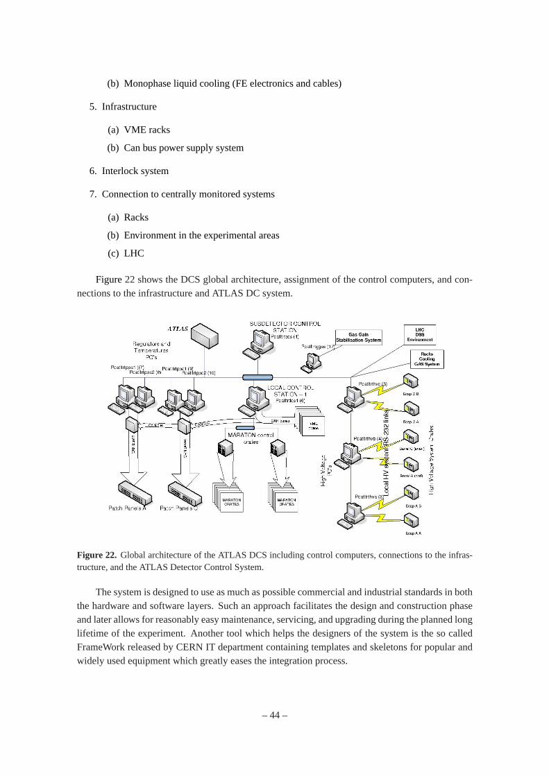
(b) Monophase liquid cooling (FE electronics and cables)
5. Infrastructure
(a) VME racks
(b) Can bus power supply system
6. Interlock system
7. Connection to centrally monitored systems
(a) Racks
(b) Environment in the experimental areas
(c) LHC
Figure22 shows the DCS global architecture, assignment of the control computers, and con-nections to the infrastructure and ATLAS DC system.
Figure 22. Global architecture of the ATLAS DCS including control computers, connections to the infras-tructure, and the ATLAS Detector Control System.
The system is designed to use as much as possible commercial and industrial standards in boththe hardware and software layers. Such an approach facilitates the design and construction phaseand later allows for reasonably easy maintenance, servicing, and upgrading during the planned longlifetime of the experiment. Another tool which helps the designers of the system is the so calledFrameWork released by CERN IT department containing templates and skeletons for popular andwidely used equipment which greatly eases the integration process.
– 44 –

8.2 Tools and methods
8.2.1 PVSS
PVSS II [15] is a SCADA system. SCADA stands for Supervisory Control And Data Acquisition.PVSS is used to connect to hardware (or software) devices, acquire the data they produce and usethat data for task supervision, i.e. to monitor device behaviour and to initialize, configure andoperate those devices. In order to do this PVSS provides the following main components and tools:
A run time database where the data coming from the devices is stored, and can be accessed forprocessing, visualization, and other purposes.
Archiving Data in the run-time database can be archived for long term storage, and retrievedlater by user interfaces or other processes.
Alarm Generation and Handling Alarms can be generated be defining conditions applying tonew data arriving in PVSS. The alarms are stored in an alarm database and can be selectivelydisplayed by an Alarm display. Alarms can also be filtered summarized, etc.
A Graphical Editor (GEDI/NG) Allowing users to design and implement their own user inter-faces (panels).
A Scripting Language Allows users to interact with the data stored in the database, either froma user interface or from a “background” process. PVSS scripts are calledCTRL (read control)scripts and follow the C syntax and include many SCADA-specific functions.
A Graphical Parameterization tool (PARA) Allowing users to:
• Define the structure of the database
• Define which data should be archived
• Define which data, if any, coming from a device should generate alarms
• etc.
Drivers Providing the connection between PVSS and hardware or software devices to be super-vised. Common drivers that are provided with PVSS are OPC, ProfiBus, CanBus, Modbus TCP/IPand Applicom. A DIM driver is provided as part of the Framework.
PVSS has a highly distributed architecture. A PVSS application is composed of several pro-cesses, in PVSS nomenclature: Managers. These Managers communicate via a PVSS-specificprotocol over TCP/IP. Managers subscribe to data and this is then only sent on change by the EventManager, which is the heart of the system shown in Figure23..
The Event Manager (EVM) – is responsible for all communications. It receives data fromDrivers (D) and sends it to the Database Manager to be stored in the data base. However, it main-tains the Sprocess imageT in memory, i.e. the current value of all the data. It also ensures thedistribution of data to all Managers which have subscribed to this data. The DataBase Manager(DBM) U provides the interface to the (run-time) data base. User Interface Managers (UIM)U canget device data from the database, or send data to the database to be sent to the devices, they can
– 45 –
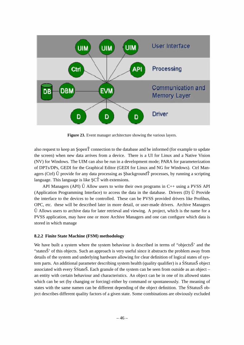
Figure 23. Event manager architecture showing the various layers.
also request to keep an SopenT connection to the database and be informed (for example to updatethe screen) when new data arrives from a device. There is a UI for Linux and a Native Vision(NV) for Windows. The UIM can also be run in a development mode; PARA for parameterizationof DPTs/DPs, GEDI for the Graphical Editor (GEDI for Linux and NG for Windows). Ctrl Man-agers (Ctrl)U provide for any data processing as SbackgroundT processes, by running a scriptinglanguage. This language is like SCT with extensions.
API Managers (API)U Allow users to write their own programs in C++ using a PVSS API(Application Programming Interface) to access the data in the database. Drivers (D)U Providethe interface to the devices to be controlled. These can be PVSS provided drivers like Profibus,OPC, etc. these will be described later in more detail, or user-made drivers. Archive ManagersU Allows users to archive data for later retrieval and viewing. A project, which is the name for aPVSS application, may have one or more Archive Managers and one can configure which data isstored in which manage
8.2.2 Finite State Machine (FSM) methodology
We have built a system where the system behaviour is described in terms of “objectsŠ’ and the“statesŠ’ of this objects. Such an approach is very useful since it abstracts the problem away fromdetails of the system and underlying hardware allowing for clear definition of logical states of sys-tem parts. An additional parameter describing system health (quality qualifier) is aSStatusŠ objectassociated with everySStateŠ. Each granule of the system can be seen from outside as an object –an entity with certain behaviour and characteristics. An object can be in one of its allowed stateswhich can be set (by changing or forcing) either by command or spontaneously. The meaning ofstates with the same namen can be different depending of the object definition. TheSStatusŠ ob-ject describes different quality factors of a given state. Some combinations are obviously excluded
– 46 –

(ex. SREADYŠ state withSFATALŠ status). The set of commands used in the system should behierarchical and adapted to the level of access. Some commands are restricted to certain categoryof user (password protected). Each command calls for certain actions, which should at lowest levelreach the smallest addressed granules (objects) of the system. Not all commands change the objectstate e.g. those changing parameters or reading status.
As an example we show in Figure24 the HV system states which easily can be mapped onany of the objects of which TRT detector is composed. It is clear that some objects will not attaincertain states due to theirs internal nature. Some of the states areSmandatoryŠ i.e. every object hasto be in one of this states; others areSoptionalŠ i.e. depending on the characteristics and nature theobject can be in one of this states.
Figure 24. The TRT High Voltage system state machine.
The control hierarchy of the objects is build up of the control units, logic units and device units.The first two have very similar properties except the lack of a stand-alone operation mode for logicunits. The device units represent direct connection to the hardware and need to be very carefullydesigned since have to reflect all possible behaviour of the apparatus. Whenever aSparentŠ in
– 47 –

hierarchy receives a transition command it sends it to all theSchildrenŠ in its branch. AnySchildŠpropagate the command and so on throughout the system. ASparentŠ (at any level of the hierarchy)confirms the transition only when all the children have confirmed the new state, so any errors whileperforming a state change are effectively propagated to the root node
8.3 Detector safety
8.3.1 DCS protections
The DC system monitors all slowly changing parameters which have any influence on the detectorperformance. However there is one parameter which apart from effect mentioned above is showingdetector safety. Big concentration of modern, very dense FE electronics in confined volume putsstringent criteria on the cooling system. The unexpected and uncontrolled rise of the temperatureof electronics or detector mechanics can lead to severe even disastrous consequences possibly evento detector damage. The DC system implements limits on the all of measured temperature values.There are 2 separate limit values: Warning set at 2-4 degs above normal working temperature whichserves as a signal to operator that something wrong is happening. Another oneU Alarm U set 7-10degs above working temperature causes cut of the low voltage to the affected detector/electronicspart. All the incidents are as well treated accordingly by FSM system and central DCS alarm screen.Similar philosophy is applied to the power supply voltages and currents. In case of the surpassingof alarm value the pertinent channel is switched off.
8.3.2 TRT hardware interlock
Backup protection against overheating of the TRT front-end electronics, beyond that provided bythe DCS, is guaranteed by the TRT Hardware Interlock (TRT-HWI). This system of custom elec-tronics monitors temperatures on the front-end boards read out using Negative Temperature Coef-ficient Thermistors (NTC), which also form inputs to the DCS system. If a specified number ofNTCs register temperatures above pre-determined thresholds for a user-adjustable period of time,then the system will switch off the Low Voltage (and also High Voltage, if desired) to the entireTRT. In addition, auxillary inputs to the TRT-HWI are also provided to allow other conditions (forexample, the proposed DCS watchdog status) to cut power to the TRT. The TRT-HWI is designedto be as fail-safe as possible: using no programmable logic or remotely setable parameters, whileonly being monitored, not controlled, by the DCS.
A block diagram of the major elements of theTRT-HWI is shown in Fig.25. The system itselfis comprised of two elements:
1. Comparator Boards, sitting on the PP2 boxes in UX15, which compare NTC outputs in 1/32of each end of the detector to pre-determined thresholds and send out current approximatelyproportional to the number of NTCs over threshold in the barrel and the endcap
2. the Logic Box, located in USA15, which is itself composed of two elements:Receiver Boardsthat receive all of the outputs of the Comparator Boards for the A and C sides of the detector,and “count” Comparator Boards with more than a specified number of NTCs over threshold;and anAlarm Boardthat uses the “counts” from each Receiver Board, as well as auxillaryinputs to generate aKILL signal based on a simple algorithm.
– 48 –

The TRT-HWI KILL signal is sent to the LV and HV control racks in USA15, disabling theiroutputs and thus switching off power to the entire TRT. The system is designed such that a failurein any component – NTC, cable, board – will contribute to (in the case of a single NTC failure) orproduce aKILL signal.
Figure 25. Block diagram of the TRT-HWI system.
Comparator Boards Each of the 64 Comparator Board receives input from a total of 28 NTCsmounted on TRT front-end electronics boards: eight from the barrel and 20 from the endcaps.These NTC signals are routed to the Comparator Boards from the TTC PP2 boards where they arepassively split off from the main TTC DCS path. On the Comparator Boards, the output signalfrom the NTCs is compared to thresholds using rad-tolerant comparators (LM339). The input tothe comparators from the NTCs is pulled down to ground, so that both shorted and disconnectedNTCs appear, to the comparator, to be in a high-temperature state, thus potentially causing aKILL
signal to be generated.
Thresholds for all barrel and endcap NTC comparators can be set independently using twosocketed resistors on the Comparator Board. This scheme allows the thresholds to be adjusted ifconditions change, but prevents them from being set remotely to incorrect values. The state of eachcomparator (above or below threshold) is indicated by an LED.
The output of all eight barrel comparators and all 20 endcap comparators are summed sepa-rately to form the two primary board outputs:BR_SUMandEC_SUM. These sums contain a smallcurrent offset to allow disconnected cables to be detected at the Logic Box.
If a given NTC is known to be bad, its comparator output can be individually removed fromthe sum (disabled) using a set of switches mounted on the board.
TheBR_SUMandEC_SUMoutputs can be used in two ways, although both methods will notbe used simultaneously.
– 49 –

1. They can be sent to theLogic Boxfor use in constructing the globalKILL signal.
2. They can be sent, via another set of comparators, to disable inputs on the PP2 Maraton powersupplies switching off LV power to the front-end boards controlled by the PP2 in question(LOCAL_KILL ).
Output to the Logic Box is accomplished differentially using two wire pairs each (forBR_SUM
andEC_SUM) on∼100 m ethernet-style cables. The alternateLOCAL_KILL signal, which is usedduring commissioning, is generated by two other comparators, the threshold for each of which canbe set using socketed resistors. TwoLOCAL_KILL signals (for barrel and end-cap) are sent outthrough LEMO connectors. The end-cap signal is split with a simple “T” to accommodate the twoend-cap LV boards in a PP2 crate.
The Comparator Boards, which are implemented on 75× 125 mm, four layer PCBs, arecollected at each PP2 location into mechanical housings, which can hold five or eight boards. Thishousing is screwed onto the side of the PP2 structure. The Comparator Boards receive power, viaa daisy-chain connector, from the same LV supply used to power the PP2 TTCs.
The Logic Box After traveling from UX15 to USA15, Comparator Board output signals arereceived by instrumentation amps on one of twoReceiver Boardsthat are part of theLogic Box:one dealing with signals from side A and one for side C. After reception each Comparator Boardoutput sum serves as input to two comparators: one which detects whether the cable from thatComparator Board is disconnected and another that compares the signal to a multiplicity threshold,set separately, by socketed resistors, for barrel and endcap sums. The results of the two comparatorsfor each Comparator Board input are summed to give two output signals,BR_MULT_SUMandEC_MULT_SUMcorresponding to the number of Comparator Boards in the barrel and end-cap thathave more NTCs over threshold than that specified by the multiplicity threshold.
Individual Comparator Board inputs can be excluded from this sum (disabled) using switcheson the Receiver Board. Because this action would leave a significant portion of the electronicsunprotected, several levels of monitoring have been added to the Receiver Boards including LEDvisual indicators and independent monitoring by DCS to ensure that disabled boards do not gounnoticed.
TheBR_MULT_SUMandEC_MULT_SUMsignals from each Receiver Board are daisy chained(effectively summing them from each board) and sent by a short ribbon cable to the Alarm Board,where they are compared against barrel and end-cap board-count thresholds, again set by socketedresistors. If any of the barrel, end-cap, or auxillary inputs are over their respective thresholds, thenanALARMcondition is generated. To reduce sensitivity to transient noise in the system, thisALARM
condition is only translated into theKILL signal if it persists for a specified period of time (set byan RC circuit, and currently∼45 s). TheKILL signal activates a relay, which produces the signalto turn off power to the TRT, via a cable to the LV (and possibly HV) racks in USA15.
Critical voltages and signals (the various SUM, ALARM, KILL, DISABLED, etc.) are mon-itored by a set of five ELMBs. One ELMB monitors the Alarm Board states and settings and foreach side, A and C, of the detector two ELMBs monitor the _SUM voltages and disabled states ofthe 32 sectors. A PVSS panel integrated into the DCS framework monitors and logs all abnormalconditions.
– 50 –

In order to be able to bring the TRT up after a power failure or a trip, it is necessary totemporarily disable the TRT-HWI. This can be accomplished by two means. First (and normally)a push-button disable is provided on the front of the Alarm Board. When pressed, this disables theKILL output signal for approximately five minutes, after which time the signal is automaticallyre-enabled and can again cause TRT power to be cut. For those occasions when a longer period ofinactivity is desired, a “hidden” switch is also provided that disablesKILL until it is put back intoits enabled position.
– 51 –

Part III
Back End Electronics, DAQ and Power
9. Timing, Trigger, Control (TTC)
9.1 Introduction
The ATLAS timing, trigger and control signals (LHC Bunch Clock [BC], level-1 accept triggersignal [L1A], synchronisation signals [Bunch and event counter resets, BCR and ECR], tests andcalibration pulses, resets, etc.) are distributed by the RD12 [16] optical TTC system. In the innertracker, this system is used up to the level of the read-out drivers (ROD) where a protocol change isdone, allowing to minimise the required functionality at the front-end level to its strict minimum.The protocol conversion is done in the TRT-TTC module [17] housed in the ROD crates. Thismodule interfaces the backbone TTC system to:
• The RODs in providing them with the BC, the L1A, the event identifier, the bunch crossingidentifier, the BCR (Bunch Counter Reset) and the trigger-type word;
• The front-end electronics read-out chips (DTMROC) in providing them with the Hard-resetsignal and in an encoded way the timing trigger and control signals. This module also re-ceives commands via VME bus, and triggers via the VME bus, the TTC optical link and themodule front panel.
9.2 The TRT-TTC and the TRT detector
9.2.1 Context
An overview of the TRT read-out system is shown in Fig.26. The TRT on-detector active elec-tronics consists of front-end boards composed of the ASDBLR and DTMROC custom chipset.
The chips are arranged on detector mounted printed circuit boards in modular groups of 10 to18 DTMROCs depending upon the particular geometry of each region of the TRT detector. Eachgroup (or board) is then linked via twisted pair cables to the off-detector electronics.The on-detector electronics are joined to the off-detector electronics via a Patch Panel which repeatsthe LVDS signals and provides trigger and control signals connectivity to the TRT-TTCs via 50-pair twisted pair cables that run approximately 100m. The optical fibers are used for bringing thedata to the ROD module.The off-detector electronics is comprised of the Timing and Trigger Control (TRT-TTC) module,the Readout Driver (ROD) and the Readout Buffer (ROB). The readout system provides timingand control signals to the front end with timing information distributed to a precision of 0.5 nsec.The system must be partitionable such that subsets of the electronics can provide data acquisitionneeds during fabrication of the detector modules and such that different portions of the TRT orInner Detector can operate autonomously during the commissioning and debugging phase of theexperiment. To satisfy these requirements, the off-detector readout and control system is a modular,VME-crate based solution. Groups of TTC and ROD modules are placed in VME crate together
– 52 –
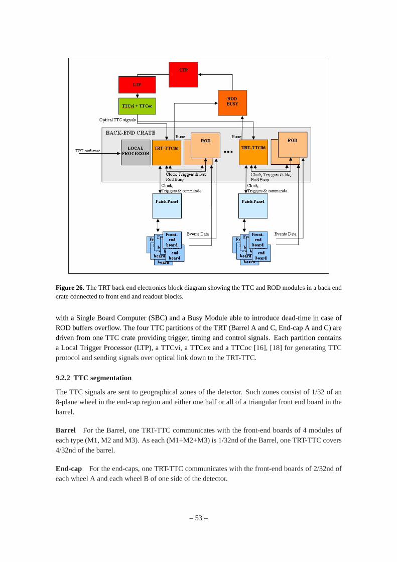
Figure 26. The TRT back end electronics block diagram showing the TTC and ROD modules in a back endcrate connected to front end and readout blocks.
with a Single Board Computer (SBC) and a Busy Module able to introduce dead-time in case ofROD buffers overflow. The four TTC partitions of the TRT (Barrel A and C, End-cap A and C) aredriven from one TTC crate providing trigger, timing and control signals. Each partition containsa Local Trigger Processor (LTP), a TTCvi, a TTCex and a TTCoc [16], [18] for generating TTCprotocol and sending signals over optical link down to the TRT-TTC.
9.2.2 TTC segmentation
The TTC signals are sent to geographical zones of the detector. Such zones consist of 1/32 of an8-plane wheel in the end-cap region and either one half or all of a triangular front end board in thebarrel.
Barrel For the Barrel, one TRT-TTC communicates with the front-end boards of 4 modules ofeach type (M1, M2 and M3). As each (M1+M2+M3) is 1/32nd of the Barrel, one TRT-TTC covers4/32nd of the barrel.
End-cap For the end-caps, one TRT-TTC communicates with the front-end boards of 2/32nd ofeach wheel A and each wheel B of one side of the detector.
– 53 –

Figure 27. TRT-TTC06 partition in the Barrel
Figure 28. TRT-TTC06 partition in the end-cap
9.3 TRT-TTC interfaces and functionality
This module is used to implement TTC [16] and TRT specific command functions and parameterloading for front-end electronics. It receives one encoded TTC signal over an optical line fromthe TTC modules [16] and a TTCrx chip [19] decodes this signal. It extracts the Bunch Clock(BC), the Level-1 Accept Trigger, the Bunch Counter Reset (BCR) and the Event Counter Reset(ECR) commands and receives trigger type information. Through the custom lines it downloadsparameters to the front-end electronics. There are 40 TTC links arranged on 4 connectors servedby the module in total. It distributes the clock and commands both to the front-end electronicsand the ROD modules. All lines to the front-end electronics have adjustable delay. For test beamand system tests purposes it can receive commands from the front panel (NIM). For dead timemonitoring purposes it measures the duration of the BUSY signals generated by the S-LINK andthe on-board buffers control. A combined BUSY signal is sent to the Central Trigger Processorthrough a BUSY module.
9.3.1 Modes of operation
TRT-TTC module provides number of different modes for writing and reading back parameters andstatus to and from the front-end. The basic one is the direct access from VME bus which is adequatefor system test. For downloading all parameters to the detector this mode would be too slow, so aso-called INIT mode is implemented. Upon receiving this command, the TRT-TTC module writes
– 54 –

Figure 29. The TRT-TTC06 VME Module
all parameters to the front-end on all TTC links simultaneously; parameters are stored in the boardmemory. Optionally, in this mode the board can read-back the parameters and compare them withexpected values.During data taking, it is expected that some register content on front-end electronics would becorrupted due to the radiation effects (single event upsets). The TTC module provides either apolling mode for checking the content of all registers or a refreshing mode for periodic refresh ofall registers. For the refresh mode gaps in the LHC beam structure are used to avoid interferingwith triggers.
DTMROC chips can be switched to Fast OR mode for cosmic trigger purposes. In this mode,TRT-TTC modules receives Fast OR signals on parameter read-back lines and forms a trigger usinga simple on-board logic. For a more complicated trigger building it further propagates Fast OR linesto VME P2 connector where a dedicated extension module can be plugged.
9.3.2 Interfaces
VME interface The TRT-TTC06 module is a 9U VME64x board, using J1, J2 and J3 connectors.Except the standard predefined pins, the user pins of J2 connectors are dedicated to the ’FAST-OR’signals described in the ’modes of operation’ section. The J3 connector is fully dedicated to thecommunication between TRT-TTC and its two RODs. 32 bits of address and 32 bits of data areused to communicate with the VME crate processor. This interface allows the communication withthe front-end boards (a change of protocol is done inside the board), reading of the status registersof the module and transmission of fake signals for calibration or system test.
TTC interface The TRT-TTC06 board is equipped with a photodiode and a TTCrx (Timing,Trigger and Control signal decoder), configurable via the VME bus (converted to I2C protocolby the Board manager). It decodes incoming TTC signal and delivers the Bunch Clock, Level1Accept Trigger, Bunch Counter Reset, Event Counter Reset, data and commands (trigger type andeventually TestPulse if this command can be sent by the LTP) to be transmitted to the front-endboards and to the ROD modules.
– 55 –

Frontend interface The front-end electronics (and in particular the DTMROC chips) need toreceive the following information from the TRT-TTC06 module: Bunch Clock, Level-1 AcceptTrigger, Event Counter Reset and Bunch Counter Reset, Test Pulses for calibration purpose, HardReset, and, of course, the parameters to configure the chips registers values. These signals andvalues are transmitted with a protocol defined by the DTMROC chips, and which is composed offour lines (command, read-back, clock and hard reset). Forty front-end boards (each housing up to15 DTMROC chips) can independently communicate with one TRT-TTC06. The clock and hard-reset lines (broadcast) are common for ten front-end boards and are fanned out at the TTC PatchPanel6. However, each front-end board has its own dedicated command and read-back lines. TheTRT-TTC06 also controls the I2C interfaces to the TTC Patch Panel to remotely adjust the BunchClock phase for each front-end board.The communication to the front-end boards is done through four cables which can be of variouslengths up to 100m. This requires a complete set of timing and transmission adjustments. In addi-tion to the Bunch Clock remote phase adjustment (by 0.5ns steps), the duty cycle of Bunch Clocksignal can also be changed, as well as its polarity. Another local fine adjustment of the BunchClock phase per ten front-end boards is also provided. Each command line can also be finelyphase-shifted, and the read-back lines can be latched at any of four different steps of 6ns each.Of course, in terms of timing adjustment for data alignment purpose, the trigger and reset sig-nals can be delayed by a multiple number of Bunch Clocks periods. These adjustments are doneindependently for each front-end board.
ROD interface The TRT-TTC06 board communicates with its two adjacent ROD boards, via theJ3 connector of the VME backplane. It transmits the trigger and synchronization related signals(Bunch Counter Reset and Event Counter Reset as well as, for every Level1 Accept trigger, thecorresponding trigger ID, Trigger Type, and Bunch Clock ID). The TRT-TTC receives from thetwo RODs the BUSY signals to be retransmitted to the Central Trigger Processor via a lemo cableconnected on the front panel.
9.4 Integration in the system and performance
The functionality of all interfaces was tested first in lab conditions using prototypes of Patch Panelsand ROD module and frontend boards from 1/32 of endcap. A small system was setup in ATLAS pitand run with DAQ. Several programs were written for performing delay scans with the system, forchecking functionality of the module in situ, etc. It was shown that TRT-TTC module is providingrequired functionality, mostly with modest L1A speeds, but also with full rate of L1A approaching100kHz.
10. Readout drivers (ROD)
10.1 Introduction
The TRT Readout Drivers (RODs) are the data processors of the TRT Data Acquisition system. AROD connects to the front-end electronics via data patch panels, to TTCs for triggers and clocks,to the Level 2 Readout Systems and to VME-based readout single board computers, as shown inFig. 26. The main function of the ROD is to receive data from the front-end boards via the data
– 56 –

patch panel (see Sec.7), check the validity of the data, compress the data, format and build thedata into mini event fragments and output the event to the Readout System (ROS). In addition,the RODs allow sampling of the events via VME-base single board computers (SBCs) for in-cratemonitoring. The RODs also send clock and control information to the data patch panels, receivetrigger information from local TRT-TTCs (see Sec.9) and assert busy when the readout systemcannot accept any more data.
The TRT DAQ contains 96 RODs in total, 32 for the TRT Barrel (16 per end), each handling2/32 of one end of the detector, and 64 for the Endcaps, with each ROD serving 1/32 of an endcapunit.
Each ROD is connected to two identical patch panels, and much of the ROD is divided intotwo logical sections, one for each data source. The ROD interfaces to each patch panel via 4 1.6GHz optical transceivers and two Cat5 ethernet cables containing clock and control information,for a total of 8 optical links and 4 ethernet cables per ROD.
The ROD is a 16 layer, 9Ux400mm deep single-width VME-based board. All external inter-faces are located on the front panel. Most of the ROD functionality is implemented within 5 XilinxFPGAs. An XC3S400 Spartan 3 FPGA handles the VME-bus protocol and translates it to a simplelocal bus for communication with the other FPGAs on board. A second XC3S400 implementsthe interface with the TTC, and handles other miscellaneous tasks. A Virtex II Pro XC2VP7 isresponsible for decoding the 8 optical input data streams, providing test data for checking the dataprocessing and interfacing to the output SLINK daughtercards. Finally, two Virtex 4 XC4VLX40chips each handle one half of the data processing (one for each data patch panel connected), con-trol the data buffering and compression, check for errors and build the data into formatted eventfragments.
10.2 ROD-TTC communication
Each TRT-TTC communicates to two RODs via a custom J3 backplane. The timing, trigger andbusy signals are sent and received from each ROD using dedicated point-to-point connections (seeSec.9). The ROD receives the LHC clock from the TRT-TTC, which is then passed through theon-board QPLL to reduce jitter. Upon receipt of a Level 1 trigger accept (L1A), the TRT-TTCsends the ROD the L1A signal, L1 identification counter (L1ID), Buch crossing identifier (BCID)and Trigger Type via a 16-bit data bus. These signals are used to ensure each subdetector’s data issynchronized with the rest of the detector, and to check each front-end chip is reading out the correctbunch crossing’s data. If the Level 2 Readout system asserts busy via the SLINK (see below), theROD asserts BUSY to the TTC which alerts the trigger system to supress further triggers. Inaddition, the ROD can assert a separate BUSY if it needs to halt triggers for internal reasons.
10.3 ROD-patch panel communication
Each ROD is connected to two independent data patch panels that service up to 120 front-endDTRMOC chips. The data from 30 DTMROCs are concentrated onto one optical fiber, resultingin 4 fibers per patch panel, each carrying 1.2 Gbits/s of data. This data is latched and 8b/10bencoded by 4 GOL [13] chips operating at 40 MHz, so the actual frequency of each fiber is 1.6GHz. The GOLs require low-jitter clocks, and each group of 30 data lines has slightly different
– 57 –

timing. To maximize the system stability, the ROD transmits the phase-locked 40MHz LHC clockvia one of the Cat5 ethernet cables to the patch panel. Each ethernet cable has 4 twisted pairs ofwire for carrying signals. The clock from the ROD is passed through a 4-channel Delay25 chip onthe patch panel, allowing each optical link to have an individual phase adjustment of its clock formaximum timing headroom. The configuration of the GOL and Delay25 chips on the patch panelis implemented via an I2C interface carried on the ethernet cables. In addition, voltage inhibits forpower sequencing, a patch-panel reset signal and an optical IDLE pattern enable are also trasmittedover the cables.
The patch panel logic is implemented within the Spartan 3 FPGA that also handles the TRT-TTC interface.
10.4 Data flow
Each data patch panel reads out data from either 120 (Endcaps) or 104 (Barrel) DTMROCs, soeach ROD handles either 240 or 208 inputs. In either case the RODs are identical – 32 channelsare simply unused when operating in Barrel mode. Each DTMROC transmits 12 bits of headerinformation and the data from 16 straws, at 25 ns/bit, meaning each ROD handles the data from upto 3840 straws.
The data from the 8 optical inputs is received using Finisar FTRJ8519 transceivers and passedto a single Xilinx Virtex II Pro which has 8 RocketIO blocks. Each RocketIO block can indepen-dently align, decode and perform a serial to parallel conversion on its data stream. After deseri-alization, data from each patch panel is split and sent to one of two Virtex 4 FPGAs for furtherprocessing.
The Virtex 4 FPGAs must first extract the header information from each of the 120 data streamsfrom the front-end DTMROCs, and further deserialize the following 16 straw’s data into 16 27-bitwide words. At this point the data is stored into DRAM for buffering, as the time taken to compressthis data varies from event to event depending on its complexity.
The DRAM consists of four 16-bit wide 256 Mbit DDR (dual data rate) memory moduleswith a maximum frequency of 200 MHz organized into a 64-bit wide bus. Raw data is written two27-bit words at a time. The controller is implemented in the Virtex 4 FPGA, with read and writescheduling optimized to minimize latency penalties due to mode switching, while ensuring priorityfor data writes when needed. As the data is read/written on both the rising and falling clock edges,the bandwidth in/out of the memory buffer is 800 M 27-bit words/sec, less the time spent in refreshcycles. Since each ROD half must process approximately 200 M straw words/sec at the maximumLevel 1 trigger rate, this leaves ample headroom.
After retrieval of the event data from DRAM, the header information is checked against theL1ID and BCID received from the TTC to ensure data synchronization across the detector. Errors,channels without data, etc, are flagged and built into an error block which is appended onto theevent data during the event building phase. The data words are first sent to the compression enginedescribed below before being passed to the event builder.
Once the full event fragment, with header, data block and error block has been assembled, itis sent back to the Virtex II Pro chip which contains the code to interface to the SLINK readoutinto the L2 Readout System (ROS). There are two SLINKs daughtercards on board (one for eachhalf-ROD’s data) that can each transmit at 160 MBytes/s via a duplex optical fiber. The ROS can
– 58 –
inhibit data output by asserting Link Full, in which case the ROD stops sending data and assertsBUSY to the TRT-TTC module. Data flow is immediately resumed once the ROS de-asserts LinkFull. In addition, a fraction of the events may be stored into DRAM as “spy” data, which can bereadout on demand over VME to the Single board computer in the crate for monitoring.
10.5 Compression
The data from each of the 350k straws is read out from the DTMROCs on every Level 1 trigger,at a rate of up to 100 kHz. Each straw’s data consists of 27 bits (see Sec.2.4), for a total of 1Tbit/s of data. This is beyond the bandwidth of the subsequent parts of the DAQ system, as wellas the storage system, and so a data compression/zero suppression scheme must be implemented.By studying the “entropy” of the data,i.e. the actual information content of our digitized data, wefound that a completely lossless compression scheme is possible, and fits well within the availablebandwidth of the DAQ chain. Since the entropy of the data stream varies logarithmically with thecomplexity of the data, there is only modest growth in the data volume from low to high luminosityconditions, and one compression works scheme for both. This compression also allows us tomonitor the detector performance via VME-based readout at a higher rate than otherwise wouldbe possible.
The entropy-based compression scheme is implemented as a Huffman encoding of the data.While each straw’s data is a 27-bit pattern, the actual number of bit patterns that actually occur isa very small fraction of the total number of 227 possible patterns. Ideally, one expects the trackingdata from each straw to be quite simple. For example, the data is all zeros if there was no particlecrossing the straw, and no noise pickup. Since the per-straw occupancy varies from a few percentat low LHC luminosity to approximately 50% at high-luminosity in the inner regions, this is themost common pattern. If a particle did intersect the straw, the data bits are zero for the time-slicesbefore the closest ionization reaches the sense wire. Once the charge does reach the sense wire, thesignal goes above threshold and the data bits are 1 until the farthest ionization (at the straw wall)reaches the sense wire, after which the data bits are again 0 (see Sec.2). In practice many morecomplicated patterns are present (approximately 100,000 in total), though the least likely may onlyoccur at a rate of less than 1 in 108. These bit patterns of data are ordered by their likelihood ofoccuring, and assigned a variable-length encoding based on this ranking. Very likely patterns getshort encodings, and rare patterns get longer ones. The Huffman encoding algorithm generatesthe table of these encodings in a way that results in an output data stream that is very close to thetheoretical minimum length to losslessly transmit the data.
The implementation of this scheme at the high rates needed (200 M lookups/s) uses an IDT75K62100,a specialized Network Search Engine (NSE) ASIC that was developed for internet routers. Two ofthese chips, operating with custom firmware in the ROD’s Virtex 4 FPGAs, allow for deadtimeless,lossless compression of the TRT data that approaches the theoretical limit.
The NSE is programmed via VME with the 128k most common 27-bit data patterns. A parallel128k deep SRAM is loaded with the encoding for each pattern as well as the code length. Inoperation, the 27-bit data pattern from a straw channel is presented to the NSE, which searches forthe table address holding the data pattern. This address is used as a lookup into the SRAM whichthen drives the encoding and code length for this data pattern. The variable-length code is read bythe Virtex 4 chip, then packed into 32-bit words and passed to the event-builder subblock. Patterns
– 59 –
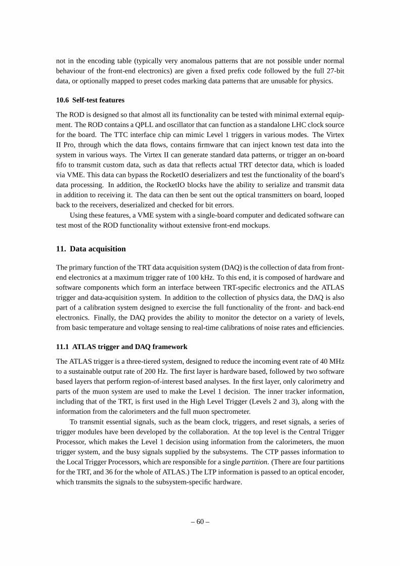
not in the encoding table (typically very anomalous patterns that are not possible under normalbehaviour of the front-end electronics) are given a fixed prefix code followed by the full 27-bitdata, or optionally mapped to preset codes marking data patterns that are unusable for physics.
10.6 Self-test features
The ROD is designed so that almost all its functionality can be tested with minimal external equip-ment. The ROD contains a QPLL and oscillator that can function as a standalone LHC clock sourcefor the board. The TTC interface chip can mimic Level 1 triggers in various modes. The VirtexII Pro, through which the data flows, contains firmware that can inject known test data into thesystem in various ways. The Virtex II can generate standard data patterns, or trigger an on-boardfifo to transmit custom data, such as data that reflects actual TRT detector data, which is loadedvia VME. This data can bypass the RocketIO deserializers and test the functionality of the board’sdata processing. In addition, the RocketIO blocks have the ability to serialize and transmit datain addition to receiving it. The data can then be sent out the optical transmitters on board, loopedback to the receivers, deserialized and checked for bit errors.
Using these features, a VME system with a single-board computer and dedicated software cantest most of the ROD functionality without extensive front-end mockups.
11. Data acquisition
The primary function of the TRT data acquisition system (DAQ) is the collection of data from front-end electronics at a maximum trigger rate of 100 kHz. To this end, it is composed of hardware andsoftware components which form an interface between TRT-specific electronics and the ATLAStrigger and data-acquisition system. In addition to the collection of physics data, the DAQ is alsopart of a calibration system designed to exercise the full functionality of the front- and back-endelectronics. Finally, the DAQ provides the ability to monitor the detector on a variety of levels,from basic temperature and voltage sensing to real-time calibrations of noise rates and efficiencies.
11.1 ATLAS trigger and DAQ framework
The ATLAS trigger is a three-tiered system, designed to reduce the incoming event rate of 40 MHzto a sustainable output rate of 200 Hz. The first layer is hardware based, followed by two softwarebased layers that perform region-of-interest based analyses. In the first layer, only calorimetry andparts of the muon system are used to make the Level 1 decision. The inner tracker information,including that of the TRT, is first used in the High Level Trigger (Levels 2 and 3), along with theinformation from the calorimeters and the full muon spectrometer.
To transmit essential signals, such as the beam clock, triggers, and reset signals, a series oftrigger modules have been developed by the collaboration. At the top level is the Central TriggerProcessor, which makes the Level 1 decision using information from the calorimeters, the muontrigger system, and the busy signals supplied by the subsystems. The CTP passes information tothe Local Trigger Processors, which are responsible for a singlepartition. (There are four partitionsfor the TRT, and 36 for the whole of ATLAS.) The LTP information is passed to an optical encoder,which transmits the signals to the subsystem-specific hardware.
– 60 –

The ATLAS experiment has created a data acquisition framework to facilitate the integration ofthe different subsystems. The system is a C++ based Finite State Machine, and uses a combinationof gigabit ethernet and fiberoptic connections to join the different parts of the experiment. Eachsubsystem is required to maintain their own dedicated hardware, and to supply a collection oflibraries which guide the hardware through the state transitions before, during, and following aphysics or calibration run.
As the interface between the ATLAS DAQ and the TRT, the TRT DAQ has the responsibility ofreceiving the Level 1 trigger decisions, processing those triggers, and returning the correspondingdata buffers to the High Level Triggers with minimal latency.
11.2 TRT scope and configuration
The TRT is composed of over 250,000 straws, ranging in length from 50cm (endcap) to 150cm(barrel). The analog readout is performed by a custom-designed ASIC which performs amplifi-cation, shaping, discrimination, and base-line restoration (ASDBLR – section1). These analogresults are sampled by a second ASIC, the DTMROC (see section2), which makes the time mea-surement of the signals and provides a digitized result to off-detector electronics for up to 16 strawchannels.
Control of the DTMROCs is supplied by the TRT TTC (see section9) each of which managesup to 480 DTMROCs. The readout of the DTMROCs is performed by the TRT RODs (see sec-tion 10). Both the TTCs and the RODs are single-width 9U VME64x modules, the entire collectionof which fill 10 VME crates for the whole detector (96 RODs and 48 TTCs). Each VME crate iscontrolled by a single board computer running a customized linux operating system.
For each piece of configurable hardware (DTMROC, TTC, ROD) a software library has beencreated. The libraries are implemented in C/C++, and provide access to all of the functionality ofthe hardware. These libraries are used on the single board computers, and interface with a VMEdriver (and the associated API) to communicate with the hardware.
The configuration parameters for all of the electronics are stored in a database, and the specificparameters used in a given run are archived for future reference. The “Configuration Database”uses an Oracle back-end, which the DAQ accesses via OKS (Object Kernel Source). This is anATLAS-specific interface which represents the hardware configuration as a completely relationaldatabase.
11.3 Readout scheme
11.3.1 Physics data
When a Level 1 Accept is sent out by the ATLAS Central Trigger Processor, one of the four TRTLocal Trigger Processors receives a copy of this signal. This LTP then passes the trigger on to thenext LTP, as well as to the ROD crates for which it is responsible.
At the ROD crate, each of the TTCs will receive a copy of the trigger, and pass this trigger onto the front-end electronics. Any delays necessary to compensate for trigger latency or front-endpipeline depth will be made in the TTC.
The DTMROC at the front-end, upon receipt of the L1A, will proceed to transmit its strawdata from a pre-determined place in its pipeline. Those data will then travel over small-twisted-pair
– 61 –

wires to a series of patch panels, which receive the electrical signals and transmit them, fiberopti-cally, to the RODs in the ROD-crates.
The ROD then organizes the straw data for up to 120 DTMROCs into a single buffer, andpackages those data with: the event, run, and ROD identifiers; any error conditions detected in theDTMROC data; and markers to indicate the beginning and end of the event. Those data are thensent to local, rack-mounted computers via the S-Link protocol [20], where they will be availablefor the High Level Trigger farms, and for collection into complete ATLAS events.
In high-rate conditions, the ROD will also perform on-board compression of the straw databefore packaging. The compression scheme is a lossless, entropy based Huffman encoding, whichhas been designed to reduce the event size by a factor of 4 at a luminosity of 1034 (which becomesa factor of 16 at low luminosities). Without compression, the size of a single event for the entireTRT is 380 kB.
11.3.2 Calibration data
A principle design challenge for the TRT was the creation of high-speed, low-noise front-end elec-tronics. While these goals were met in the design phase, a thorough calibration of operating thresh-olds and straw efficiencies must be made on a routine basis in order to maintain optimal noiseperformance. Several tools have been developed to perform these calibrations. Some are suited todetailed testing, as described in section14. To test and calibrate the full detector, a collection oftools has been created within the data acquisition framework.
The calibration data is acquired in the same way as the physics data, though more supervisionis required. A run consists of a scan over some number of points in configuration space. To controlthe event rate, and to ensure adequate statistics for a given test, the trigger electronics are controlleddirectly to provide a specific number of triggers per scan point. The DTMROC event data, oncecollected by the RODs, is packaged with the necessary information to reconstruct the configurationat the time of that event. The ROD data is then collected by a dedicated computer, which eitherstores the data for later processing, or processes the data in real time.
11.3.3 Monitoring
Monitoring the activity and health of the detector is an important task which has been integratedwith the data acquisition system. In addition to monitoring changes in detector performance, theDAQ also watches environmental conditions such as chip temperature and low voltage levels onthe front end electronics, which complements the monitoring done by the Detector Controls group(see section8.1).
11.3.4 ATLAS tools and the TRT viewer
At the ATLAS level, there are several tools available to the subsystems to help with detector mon-itoring. One of which is an event display, which incorporates all of the subsystems into a single,intuitive interface. This tool, called Atlantis, is designed to show event-level data in an easy tonavigate format, with a variety of different projections available for all systems. This interface isquite nice on an event level, but in order to see detailed information about detector performanceover an entire run, another collection of tools must be used. This suite, called AthenaPT, is simi-lar in nature to the ATLAS level-3 trigger, and is capable of performing full reconstruction for all
– 62 –

subsystems. It can be run in real time, sampling complete events from the DAQ event builder andstoring the results into ROOT-based histograms for future analysis.
At the TRT level, a special tool has been developed that combines the event display capabilitiesof Atlantis with the detector performance monitoring of AthenaPT. The TRTViewer extracts theTRT information from the raw data and provides both a real-time event display and an analysispackage that does track reconstruction, efficiency calculations, noise occupancy maps, and errormonitoring. This tool will also provide an interface to the configurations database, and will havethe ability to re-calibrate detector thresholds and timing based on information extracted from themonitoring process.
11.3.5 Voltages and temperatures
The on-detector ASICs were designed with the ability to report their temperature and operatingvoltages, which are then monitored for changes over time. The temperature or voltage can be foundby searching for the threshold over which the DTMROC reports an error for the quantity beingmeasured. Similarly, crossing the threshold from the other direction causes the error condition todisappear.
As temperatures and voltages tend to behave consistently among chips that share a commonlow voltage connection, pairs of adjacent chips are used to bracket a common threshold over whichthe error condition appears. One chip will be set above threshold, and its neighbor will be set belowthe same threshold. If either chip changes state, the change will be registered for both chips, and anew threshold will be set. The error conditions are recorded during the beam gaps using the pollingmechanism in the TRT-TTCs, which allow one to request the read-back of a DTMROC register atsome future time when there will be no triggers (i.e. the beam orbit).
12. High voltage power
12.1 Requirements
The High Voltage power supply system has to deliver 1.5 to 2 kV to each straw. It is based on amulitichannel HV power supply from HVSys [21] and one HV channel delivers power to severalstraws (up to 192). In order to avoid the loss of a large fraction of the detector in case of a problemon one straw (e.g in case of a short between a wire and the straw), each group of 8 straws isindividually protected with a fuse at the level of the detector (on the WEB for the end-cap andthrough fuse boxes in the barrel). The total number of HV channels for the end-cap and the barrelis given in Table5.
Maximum DC current per HV channel The maximum current per line is defined by the numberof powered straws and the average current consumption per straw at maximum luminosity. TheTable6 summarises the requirements. The maximum current to be delivered by a HV channeltakes into account a safety factor to accommodate fluctuation in the luminosity.
Maximum AC current per HV channel The HV distribution circuit includes a filter comsistingof a 100 kOhm resistor and a 1 nF capacitor. In case of a straw discharge, the HV source mustrecharge the 1 nF capacitor through the 100 kOhm equivalent resistor sufficiently fast enough so
– 63 –

End-cap
Per wheel A 64 Per wheel B 32
Total wheels A 768 Total wheels B 512
Total End-cap 1280
Barrel
Per barrel Module-1 6 Per barrel Module-2 6
Per barrel Module-3 10
Total Barrel 704
Total 1984
Table 5. Number of HV feeds
Detectorelement
Numberof straws
Numberof lines
Numberof strawsper line
Currentper strawat full lu-minosity(mA)
Totalcurrentper line(mA)
MaximumDC cur-rent tobe deliv-ered bythe HVsource(mA)
Wheel-A 12288 64 192 0.0045 0.86 3
Wheel-B 6144 32 192 0.0045 0.86 3
Barrel-1 329 6 55 0.020 1.1 3
Barrel-2 520 6 87 0.010 0.9 3
Barrel-3 793 10 80 0.006 0.5 3
Table 6. Estimated maximum current per HV channel at full luminosity
that a discharge does not appear as a DC fluctuation. A maximum current of 16 mA during 100 msmust be delivered by the power supply.
Trip requirements When an anode wire is in contact with the cathode, the contact resistanceis in the range 0-3 kOhm and some damage can appear in the straw (e.g. holes) under someconditions. Continuous discharges (when the wire is not in direct contact with the cathode) canalso lead to damaging the straw conductive layer (dust) and in some cases a hole in the straw canappear. It has been shown that the damage appears only after more than 5000 discharges have takenplace. Limiting the number of discharges is, hence, a very important requirement. The system hasa programmable trip level and time duration for how long the trip level can be exceeded beforeactually tripping he HV output.
– 64 –

12.2 HVSys power supply
The system is a multi-channel power supply from HVSys. Contained in a 6U euromechanics crate,the system consists of up to twenty 21-channel HV modules and a crate controller. A backplanedistributes control signals and low voltage power. A view of a full crate (420 channels, 2.5 kW HVpower) is given in Figure30.
Figure 30. View of a full crate housing 420 HV channels.
The main characteristics of the power supply are given in Table7.
12.3 Implementation
The overall TRT HV power system is divided into four entities: each side of the barrel and eachend-cap. Each barrel side and each end-cap requires, respectively, 352 and 640 channels. Thepower supplies are located in the counting room (USA15). Multiwire HV cables are used up topatch panel 2 (36 or 52 wires per cable, length in the range 60 - 100 m) and then miniatiure cablesare used from the patch panel 2 location to the detector (coaxial cable of 1-mm outer diameter,length in the range 6 - 15 m). Several passive patch-panels are needed as seen on Figure31:
• One patch panel in the control room adapting the power supply 3-channel miniature LEMOconnectors to 52- or 36-way connectors attached to the multiwire HV cable;
• One in the patch panel 2 region converting between multiwire cables and miniature coaxialcables;
• On at the end of the cryostat flange for the end-cap (PFF1) and close to the barrel face beforeconnection to the fuses (PPB1) to facilitate detector installation.
12.4 Control
The TRT HV system is controlled by a microprocessor contained in the crate controller moduleas well as a microcontrollers at every module board. The basic crate architecture contains a main
– 65 –

Parameter Value ConditionNo. of independent channels 420
Output voltage per channel Programmable in therange 500 - 2000 V
In steps of 2 V
Current per channel 3 mA Maximum continuous rat-ing.
Ramp-up and Ramp-down Programmable in therange 1 -500 V/s in stepsof 10 V/s
Noise and ripple ≤50 mV pp 0-100 MHz at output witha 5k - 1 nF filter
Voltage Monitor versus Output VoltageAccuracy
±0.5 V ±0.1% of read-ing
Voltage Set versus Voltage monitor Ac-curacy
± 1 V ±0.1% of setting
Current Monitor versus Output CurrentAccuracy
± 5µA
Maximum Current Set versus OutputCurrent Monitor Accuracy
±2.5 µA
Over-current trip condition - Output voltage set to 0Vif the maximum outputcurrent value is exceededfor more than a pro-grammable time
Efficiency 80%
Table 7. HVSys power supply characteristics
Figure 31. HV distribution scheme
microprocessor and four slave microprocessors, serving as four branch controllers. Built-in controlfirmware accepts external commands and communicates with the cells. A host computer can acces
– 66 –

the crate via a serial RS-232 communication line or via optocoupled CAN-bus or USB. Two lines ofthe internal system bus are used for communication with the high voltage cells. The communicationis performed at a bit rate of about 10 kHz. The software of the dedicated branch controllers in amaster regime realizes the interchange protocol. All the cells (HVCs) operate as slaves on thebranch. The controller also controls the central power supplies LV and BV, monitors them andprovides emergency procedures . Two 8-channel analog to digital converters are implemented forthe monitoring of the central power supplies and temperatures of the critical elements. Commandsfor the controller are divided into several main groups according to their functional assignments.
• Commands for obtaining system unit status.
• Commands controlling the central power supply.
• Commands controlling cell(s).
• Cell detection commands.
• Commands addressed simultaneously to all cells.
• Service commands.
• Test commands.
The USB and CAN communication modes are rather primitive and do not exploit all the virtuesof either USB or CAN but simply translate the ’character’ based RS-232 protocol to either CAN(messages) or USB (packages) oriented media. Carefull studies of the system performance leadto a decision to abandon any control method than RS-232. To allow for easier integration of thesystem into the overall TRT DC system an OPC server for system controls was constructed aswell as a FrameWork type for the hardware devices. This allows use of all of the FrameWorktools for mass parametrization and acces to configuration and conditions databases. The systemperformance is limited by the speed of internal bus and the required overhead in the OPC servernecessary for robust error handling. The average response time for a broadcast command sent tothe 420 channels contained in a crate is 30 secs.
13. Low voltage power
The low voltage distribution to the TRT front-end electronics is based on a two level scheme shownin Figure32and described in greater detail in [22].
• Bulk power supplies deliver power to the PP2 power boards;
• PP2 power boards housing radiation tolerant voltage regulators delivering the power to thefront-end.
In order to reduce the length and hence the size of power cables, Wiener MARATON [23] radiationand magnetic field tolerant bulk supplies which can be installed in the experimental cavern (UX15)have been used.
– 67 –
Figure 32. View of the low voltage distribution system
13.1 Requirements
A bulk supply gives power to a PP2 box which is serving 1/32 of the detector (one side). There are6 location sites, housing 3, 5 or 8 PP2 boxes each. Each PP2 contains 3 power boards, one for 1/32of the barrel, one for 1/32 of the wheels A and one for 1/32 of the wheels B. In addition the PP2box contains some electronics which needs to be powered. Three different voltages are needed forthe front-end supply (+3V, -3V, +2.5V) and an additional one (5V) for the PP2 electronics. Thetotal current needed per PP2 box and voltage source is given in Table8.
+3V -3V +2.5V PP2(5V)
Barrel 13A 11A 13.5A
Wheels A 18A 16A 19A
Wheels B 12A 10.5A 12.5A
PP2 A few A
Total 43A 38A 45A A few A
Table 8. Current needed per supply
Each PP2 box will require 4 power supply channels. Because of the voltage drops introducedin all the cables (bulk to PP2 and PP2 to front-end) one need a much higher voltage at the bulksupply level than what is needed on the front-end; an 8V/300W MARATON channel has been usedfor all of them. As the needed power for the PP2 electronics is low, one MARATON channel isshared between 2 PP2 boxes. 64 PP2 boxes must be fed, leading to 224 MARATON channels (3channels per box for powering the front-end and 1 channel every 2 PP2 box for the PP2 electronics).
13.2 WIENER MARATON supplies
There are three main components in the WIENER system (as seen in Figure32):
1. 3U power crate with radiation and magnetic tolerant DC-DC each of them housing 12-channel 8 V/300 W elements;
2. 4U crate housing up to six 3.6 kW AC-DC converters (380 V DC output). One AC-DC isneeded to power a 12-channel 8 V/300 W element;
– 68 –

3. 6U crates housing up to 21 control boards. One control board controls a 12-channel 8 V/300W element.
Position 1 is in the experimental cavern (UX15), while positions 2 and 3 are in the controlroom (USA15).
In UX15 they are racks for the TRT power supplies at five locations on the structure aroundthe detector. Table9 gives the summary of the different PP2 boxes powered from each location, aswell as of the MARATON equipment needed at each place.
MARATON equipment
Location PP2 boxes location # PP2 boxes # channels # 3U power crates
1 1&2 side-C 13 46 4
2 1&2 side-A 13 46 4
3 3&4 side-A 13 46 4
4 3&4 side-C 13 46 4
5 5&6 side- A & C 12 38 4
Total 64 256 24
Table 9. MARATON devices at each location in UX15.
In order to maintain a clear path for the current returns of the power lines feeding the front-end,each DC-DC is floating and two wires (power and return) are used to feed the PP2 boxes, exceptfor the + and - 3V which are using a common return line.
13.3 Overall efficiency
There are voltage drops and inefficiencies at several levels in the system. Table10gives a summaryof the voltage drops as from the MARATON DC-DC converter. The minimum and maximumvalues correspond to different cable lengths and section; it takes into account the drop on the returnlines.
Element Voltage Drop
Type III cable 0.5 - 1 V
Regulators at PP2 0.8 - 1.5 V
Type II cables 0.5 - 1.3 V
Total maximum drop 3.8 V
Table 10.Voltage drops
In order to have 2.5 V on the front-end boards, one has to deliver up to 8.3 V at the output ofthe DC-DC converters. This gives an efficiency of 30%. Taking into account the efficiency of theAC-DC (main to 380 Vdc) and of the DC-DC (and neglecting the very small drop on the type IVcable) leads to an overall efficiency of about 20%.
– 69 –

13.4 Control
13.4.1 Bulk Supplies
The MARATON power supplies are delivered with an OPC server package which serves for theremote control of the unit. The server operates via Ethernet. The OPC standard is an interfacingmethod to avoid the need of device specific drivers. CERN control group from IT departmentprovides users with the skeleton software solution called FRAMEWORK. The package containsmany useful tools serving for construction, integration and configuration of the complex multi-channel systems build of the standard, widely available equipment. The MARATON system hasbeen included into FRAMEWORK which makes its integration very easy. The control commandsof the MARATON system are limited. Basically the only important action which can be undertakenby user is switching the given output on or off. For the monitring purposes the system gives anaccess to the values of the output voltages and currents. The control panels has been designedwhich allow user the monitoring and control of the system.
13.4.2 Patch panels
Groups of regulators supplying geographically close parts of detector front-end electronics havebeen placed on a printed circuit board together with the control and monitoring electronics. Onecard of 440x200 mm size houses up to 36 regulators (positive and negative) delivering 6/8 voltagesets :±3 V for analogue electronics and +2.5 V for digital part. Three boards are used to power a1/32 phi slice of the detector: 1 for the barrel part and two for the end-cap wheels. The high powerdissipation on the board (60-70 W) necessitates an agressive liquid cooling system, described insection4.2. The circuits on the board perform the functions described in the following paragraphs.
Voltage regulation and setting The regulators used are of the adjustable version. Changing thevoltage ’adjust’ input allows output to be set at the value assuring the proper operation of the FrontEnd electronics during life cycle of the experiment when semiconductor devices could change itscharacteristics due to radiation. The variable voltage is delivered by radiation hard DAC embeddedin the DTMROC chip (see section2. The settings of the DAC’s are controlled over simple 3-wireserial protocol. The current swing of the DAC output allows for regulators output to be variedby 0.5 V up to 1.2 V, which is fully covering expected change of the voltage supplies of FrontEnd electronics [24]. Some Front End parts draw current slightly exceeding the maximum oneallowed for the regulators (wheels A). For these channels parallel operation of the regulators hasbeen implemented. Carefully designed biasing network ensures correct sharing of current betweenthe two regulators.
Voltage and current measurements in each individual output line. The board contains em-bedded controller - an ELMB (Embedded Local Monitoring Board [11]), standard control unitdesigned for ATLAS. All voltage outputs are connected to the ELMB’s ADC allowing for outputvoltage measurements. The same ADC is measuring the output currents, by monitoring the voltagedrop on 22 mOhms serial resistors inserted in output lines.
Over current protection. The regulators have an over-current protection which, when currentdrawn exceeds designed value, operates the regulator in constant current mode. Such a state of
– 70 –

regulator is signalled by a level on one of the pins. This signal is latched by board logic and can beread-out by ELMB and if enabled will switch the affected channel off.
Enabling and disabling individual output lines (on/off) The DTMROC has an output whichvia the proper command can be set ’true’ or ’false’. This output is connected to the ’inhibit’ inputof the pertinent regulator thus providing a mean to switch the regulator output on/off. The sameinput is as well accepting the signal from over-current-monitor circuitry.
13.4.3 Control and monitoring
The TRT power supplies control system has been build upon the commercial SCADA (SystemControl And Data Acquisition) software package chosen by CERN as standard for control systemsof LHC experiments - PVSSII. Detailed description of the available tools and methods are availableelsewhere [15].
CAN bus and ELMB ELMB is a basic hardware unit of ATLAS detector control system whichcan operate in magnetic field and radiation environment of experimental cavern. It contains 64channels multiplexed to the ADC input and several I/O digital ports. Its basic functionality anddetailed description can be found elsewhere [11]. ELMB commands and monitoring readbackvalues are send over the CAN bus [25] - one of the CERN recommended commercial fieldbuses.The CAN bus, designed and widely used in automobile industry, is a very robust communicationlayer and both hardware and software components are available from wide range of manufacturers.Different autonomous actions can be taken when ELMB error condition was detected: node reboot,microcontroller firmware reload, disconnecting affected node from CAN bus. Merging the NodeIDwith MessageID codes to COBID (CAN Object ID) field allowed to set very efficient messageoriented priority mechanism. A set of broadcast messages allows reducing bus load in complexsystems.
DTMROC The DTMROC is the digital front end chip for the TRT detector. This radiation hardchip contains four 8-bit DAC’s which are used here to set the output voltage of the regulators.Writing and reading of the DTMROC registers is performed over a 3-line serial protocol (data-in,data-out, clock) which is driven by the ELMB in this application.
LVPP boards control The main development effort spend on the TRT low voltage system hasbeen directed into the design, programming and debugging of the Low Voltage Patch Panel boards(LVPP) containing the voltage regulators and main controlling/monitoring circuitry. As already hasbeen mentioned the heart of the LVPP is an ELMB communicating with the host controller overthe CAN bus. The read-out of the analogue values (current and voltage) is typical (and standard)for ELMB use and is based on the CANOpen [25] software layer where the OPC standard fordata access has been implemented. The ’analogue’ functionality of the ELMB has been includedas well into CERN FRAMEWORK package so the integration and control is reasonably easy andstraightforward. Fully custom made design was done for the control of the voltage regulators byDTMROC’s. We have designed and build an extension to the standard PVSS CTRL scriptinglanguage [15], which allows for user defined functions to be interpreted by PVSS in the same wayas PVSS functions. It consists of a set of class methods compiled into new shared library DLL,
– 71 –
providing the input, output parameters and return value. The functions access directly the CANbusdriver. The DLL contains following functionalities.
• Initialization of the CANbus, ELMB, DTMROC
– Operational:
– Set DAC’s
– Read back DAC’s
– Set inhibits in DTMROC’s
– Read back inhibit state
– Enable/disable and read out OCM state
• Diagnostics:
– Reset (soft and hard) of DTMROC’s,
– Send given number of clocks to DTMROC’s
– Get state of a given DTMROC,
– Set ELMB in the requested state
– Read back ELMB state
– Close connection
– 72 –
Part IV
Installation, Integration and Performance
14. Installation, integration and testing
The front end electronics for the TRT have undergone an extensive testing regime throughout thecourse of the installation process, testing functionality, individual noise performance, and perfor-mance inside of the larger system. There were three distinct phases of this testing regime: func-tionality tests after stuffing and burn-in, connectivity and noise tests before and after mounting theboards on the detector, and system level tests after the electronics installation was complete. Thesethree phases will be described below.
14.1 Front end board initial tests and preparation
The inital testing of the TRT Endcap Front End boards was done at the Niels Bohr Institute inCopenhagen, and the testing of the Front End boards for the TRT Barrel was done at CERN, withmanpower from the University of Pennsylvania, Lund University, and Hampton University. Aunified testing procedure was used, with testers at both locations using the same test suite, writingresults into a single MySQL database. The test suite, which was written by Ole Ro/hne [26], wasdesigned to exercise the complete functionality of each board and its corresponding chips. All ofthe registers of each DTMROC were exercised, a fine timing scan was run to check the health ofthe command lines, and a noise scan was run with the internal test pulse firing to characterize theanalog performance and identify dead channels. For the Endcap boards, a test was also run withan external pulse injector as another way to identify dead or problematic channels. The data fromthese tests were stored in the previously mentioned MySQL database, and a web interface to thisdatabase was developed for later viewing, as well as tracking board shipments and repair histories.
The cuts that were made at this stage were the following: no register/memory failures or finetiming anomalies were tolerated in the chips on any boards. For the endcap boards, no dead orotherwise non-functional channels were allowed at this stage either. For the Barrel boards, whichhad a much less forgiving granularity (up to 432 channels on a single PCB, vs 64 for the endcapboards), a cut of no more than roughly 0.5 percent dead or otherwise non-functional channels fora single board was used. All boards which passed the initial testing phase were burned in for 1week at∼ 80 degrees C at a special facility which was constructed for this purpose at NBI inCopenhagen. The burn-in facility continuously measured the current consumption of the front-endboards as well as maintaining a constant temperature through the burn-in process. After burn-in, allboards were tested a final time. Those boards which failed the tests (either before, or after burn-in)were sent to Penn for repairs, and then retuned to CERN or NBI to be inserted back into the testingprogram.
14.2 Front end board installation and tests
After passing the first round of tests, The FE Boards for both the TRT Barrel and Endcap weretransfered to the SR-1 Integration Facility at CERN to be installed on the detector. A series of testswas run on the boards at this point with two main goals: characterizing the noise profile of each
– 73 –

front end board, and ensuring that the boards were properly connected to the detector. In order tocharacterize the noise performance, three tests were run: one which recorded the low (tracking)threshold noise response for all low threshold values; a second, similar test which looked at theresponse to a calibrated internal test pulse rather than noise; and a third test which recorded thehigh (transition radiation) threshold response to the internal test pulse for all high threshold values.This series of tests was run both before and just after each board was mounted on the detector -see Fig33. Anomalies in the noise response of a given board tended to point to problems with themechanical insertion and contact of the board with the faraday shield, so particular attention waspaid to the results of these tests.
In addition to the threshold scans, other tests were done after the board was mounted to deter-mine if the channels were properly connected to their respective straws. In the barrel, a ’connec-tivity test’ was run where an external pulse was applied to the high voltage system and data fromthe corresponding pulse that was induced on the annode wires was read out to show connectivity.For the endcaps, where the design of the high voltage system made this approach impossible, thedetermination of connectivity was made through a twofold process of analyzing the difference be-tween on and off detector noise rates, and running a scan which uses the ’accumulate mode’ ofthe DTMROC to measure a background rate of high threshold hits when high voltage and activegas are applied to the detector [27]. The combination of this “accumulate mode” scan with thedifference between on and off detector noise rates provided for an equally powerful identificationof disconnected channels.
When the electronics integration was complete, the numbers of dead channels/straws were asfollows: For the Barrel, there were 1755 dead straws out of 105,088 total (1.7%), of which only 119were from dead or otherwise non-functional electronics channels. The vast majority of dead strawswere due to wires that had to be removed due to high voltage instability or physical non-conformityof the straw. For the Endcaps, Endcap C had 932 dead straws out of 122880 total (0.8%), whileendcap A had 493 (0.4%). All of these failures arose from mechanical problems, chief among thembeing failed high voltage lines. Again, the feat of having zero non-functional electronics channelswas acheived mainly as a result of the forgiving granularity of the endcap board design. The noiselevels on both the barrel and endcap sections of the detector were well within specifications, afterall electronics were installed and faraday cages completed, and the noise levels stayed constantafter the subdetectors were integrated into ATLAS.
14.3 TRT stand-alone noise and system tests
After the front-end board installation phase was complete, a phase of system level tests began,looking for noise or readout issues in the larger detector. The first of these tests was simply to lookfor increasing levels of noise as larger and larger fractions of the detector electronics were poweredand read out in unison. The front-end electronics (and especially that of the barrel) is known to havea sensitivity to clock pick-up as a result of having the 40MHz control lines in close proximity to thesensitive analog inputs, and it was a worry that as more and more clock signals were running on thedetector this pick-up would increase. When this test was first run, some regions of increased noisewere found. However, they all pointed to gaps in the outer faraday shield, and they all disappearedwhen the gaps in the shield were filled as shown in Figure34. Once the outer faraday shield was
– 74 –

Figure 33. Per channel 300kHz threshold distributions for Barrel electronics on (green), off (red), on-off(blue) the detector and then difference from chip average (purple). Note that the increase in the 300 kHzthreshold when the electronics are mounted in place is due to the detector capapcitance which raises theequivalent noise charge figure for the ASDBLR. The smaller capacitance of the first nine layers of ‘short’straws is clearly evident in the difference (blue) distribution.
completed, there was no increase in noise as a result of powering and clocking large sections of thedetector.
Another one of the concerns was that the front end electronics would be affected by pickuparising from its own data read out. To test for this susceptibility, a special trigger was set up tosend pairs of triggers, the first one being a normal noise event, and the second one taking data thatcorresponded with the time when the first event was being read out. A larger occupancy in the datafrom the second trigger would point to a sensitivity to data read-out pick-up. The result of thisstudy also depended heavily on the state of the outer faraday shield. When this test was first done,and the faraday shield was not yet complete, some chips showed a slight sensitivity to data read-outpick-up. however, the magnitude of this effect was very small, and in the barrel, it decreased tozero once the faraday cage was complete.
14.4 Combined noise tests with SCT
After internal noise issues, the main worry for the TRT electronics performance was interferenceor pick-up between the TRT and the SCT. As the two subdetectors are in such close proximity, andas their services often run one on top of the other in the cable trays leading to the detectors, greatcare was taken to isolate the two systems in the design. This approach seems to have succeeded,
– 75 –

Figure 34. A side of the TRT Barrel showing the threshold setting required to obtain a 300 kHz averagenoise rate in each channel.
as no crosstalk or interference between the two systems has been observed to date [28]. The firsttest in this domain was to simply run the TRT with a noise trigger with the SCT powered off, andthen take a second noise run with the SCT powered on. The comparison of these two states showsno difference in noise occupancy in the TRT as a result of the SCT being on or off. A second testwas to look for a sensitivity in the TRT electronics to the SCT read-out. This test was similar tothe internal TRT test for read-out pick up, except that in this case the TRT trigger was timed tocoincide with the SCT read-out cycle, rather than that of the TRT. Again, no increase in noise wasfound when the SCT was reading out as compared to when it was not. finally, the effect of a poorgrounding scheme was investigated. here, the TRT analog ground plane was attached to the SCTdigital power return ground, and a noise run was taken. once again, there was no noticable increasein noise rates, indicating that there is little sensitivity in the TRT electronics to mistaken or poorly
– 76 –

made grounding connections between the two subsystems.
14.5 Cosmic ray runs with SCT and ATLAS
In 2006, a series of cosmic ray runs was taken with the TRT and SCT combined, in the surfacebuilding (SR-1) at CERN where the two detectors were assembled and integrated [28]. The runswith the TRT and SCT barrels were taken in the spring and summer, while those with the TRT andSCT endcaps (C-side only) were taken in the fall. For the run including the TRT Barrel, 1/8 of thebarrel was read out (1/16th on top and 1/16th on bottom), comprising just over 13,000 channels. Forthe endcap run, 1/16 of the endcap was read out, comprising roughly 7500 channels. In both cases,a simple scintillator trigger was set up to highlight the active regions, and the standard ATLASDAQ and monitoring infastructure was used to record and monitor the data. These runs providedvaluable experience in commissioning, running, and monitoring the detector. In addition, the datasets that were generated were extremely useful for tracking and alignment studies as it was the firstinstance of recorded tracks in the final detector.
Once the detector was fully installed and integrated into ATLAS, the TRT participated in sev-eral global commissioning runs (the series of which is still ongoing as of this writing), again takingcosmic ray data (see Fig35), with varying portions of the detector being read out. These com-missioning runs provided valuable running experience with the final hardware setup and the globalATLAS DAQ - something that was not available before the detector was installed. In particular,methods for setting and tuning the front-end voltages, setting and tuning the tracking threshold, andfor tuning the fine timing required for proper drift-time measurement were developed. In particular,the voltage and temperature sense functionality in the DTMROC has proved essential in properlysetting up and monitoring the voltages on the front-end electronics, as this is the only direct mea-surement available of the voltage at the front-end electronics, deep within the detector. Also, thesecommissioning runs provide critical experience for the DAQ system inside of ATLAS, as well asmonitoring and data analysis.
Figure 35. Cosmic ray tracks in the TRT Barrel from the “M3” run in ATLAS using the Tile Cal trigger.
– 77 –

15. Acknowledgments
The research described in this publication was partly supported by following funding agencies: theEuropean Union (DGXII), the International Science Foundation (Grant NM5J000), the SwedishNatural Science Research Council, the Swedish Council for Planning and Coordination of Re-search, the Ministry of Science and Higher Education, Poland, the International Science and Tech-nology Centre (ISTC projects 441 and 1800P), the Civil Research and Development Foundation(Grant REC-011) and grants from the U.S. Department of Energy and the U.S. National ScienceFoundation (awards 0072686, 0301841, 9722537).
– 78 –

16. References
References
[1] ATLAS TRT Straw Drift Chamber Paper, to be published....
[2] N. Dressnandt, N. Lam, F.M. Newcomer, R. Van Berg, H.H. Williams, “Implementation of theASDBLR straw tube readout ASIC in DMILL technology,” IEEE Trans. Nucl. Sci.48, 1239(2001).
[3] T. Akessonet al. [ATLAS-TRT Collaboration], “Straw tube drift-time properties andelectronics parameters for the ATLAS TRT detector,” Nucl. Instrum. Meth. A449, 446 (2000).
[4] N. Dressnandt, F.M. Newcomer, O. Rohne, S. Passmore, “Radiation hardness: design approachand measurements of the ASDBLR ASIC for the ATLAS TRT,” Nuclear Science SymposiumConference Record, 2002 IEEE Volume 1, 10-16 Nov. 2002 Page(s):151 – 155.
[5] C. Alexanderet al., “Progress In The Development Of The DTMROC Time MeasurementChip For The Atlas Transition Radiation Tracker (Trt),” IEEE Trans. Nucl. Sci.48, 514 (2001).
[6] F. Anghinolfi et al., “DTMROC-S: Deep submicron version of the readout chip for the TRTdetector in ATLAS,”Prepared for 8th Workshop on Electronics for LHC Experiments, Colmar,France, 9-13 Sep 2002
[7] ATLAS TRT End Cap Detector, to be published....
[8] ATLAS TRT Barrel Detector, to be published...
[9] C. Baxter, T. Chandler, N. Dressnandt, C. Gay, B. Lundberg, A. Munar, G. Mayers,F.M. Newcomer, R. Van Berg, H.H. Williams, “Progress on the development of a detectormounted analog and digital readout system for the ATLAS TRT,” Nuclear Science SymposiumConference Record, 2003 IEEE Volume 1, 19-25 Oct. 2003 Page(s):202 – 205.
[10] H. Blampeyet al., “Services for the read-out of the ATLAS TRT cables types I and II, fromdetector to PP2,”Prepared for 11th Workshop on Electronics for LHC and Future Experiments(LECC 2005), Heidelberg, Germany, 12-16 September 2005
[11] http://elmb.web.cern.ch/ELMB/
[12] H. Furtado, “Delay25, an ASIC for timing adjustment in LHC”,Prepared for 11th Workshopon Electronics for LHC and future Experiments (LECC 2005), Heidelberg, Germany, 12-16September 2005http://proj-delay25.web.cern.ch/proj-delay25/delay25_-_home.htm
[13] P. Moreira, G. Cervelli, J. Christiansen, F. Faccio, A. Kluge, A. Marchioro, Thomas H. Toifl,J.P. Cachemiche, M. Menouni, M “A radiation tolerant gigabit serializer for LHC datatransmission,”7th Workshop on Electronics for LHC Experiments, Stockholm, Sweden, 10 – 14Sep 2001, pp.145-149
[14] CERN EP Microelectronic Group, http://web-micfe.web.cern.ch/web-micfe/index.html
[15] S. Schmeling, “Common tools for large experiment controls-a common approach fordeployment, maintenance, and support,” IEEE Trans. Nucl. Sci.53, 970 (2006).
[16] B. G. Taylor [RD12 Project Collaboration], “TTC distribution for LHC detectors,” IEEETrans. Nucl. Sci.45, 821 (1998).
– 79 –

[17] P. Lichardet al., “Evolution of the TRT backend and the new TRT-TTC board,”Prepared for11th Workshop on Electronics for LHC and Future Experiments (LECC 2005), Heidelberg,Germany, 12-16 September 2005
[18] P. B. Amaralet al., “The Atlas Level-1 Central Trigger System,” IEEE Trans. Nucl. Sci.52,1217 (2005).
[19] J. Christiansen, A. Marchioro, P. Moreira, A. Sancho, “Receiver ASIC for timing, trigger andcontrol distribution in LHC experiments,” Nuclear Science Symposium and Medical ImagingConference Record, 1995., 1995 IEEE Volume 1, 21-28 Oct. 1995
[20] H.C. van der Bij, R.A. McLaren, O. Boyle and G. Rubin, “S-LINK, a Data Link InterfaceSpecification for the LHC Era, IEEE Trans. Nucl. Sci.44, 398 (1997).
[21] HVSys, Dubna, Russia. http://www.hvsys.dubna.ru/
[22] Z. Hajduket al., “Distributed low voltage power supply system for front end electronics of theTRT detector in ATLAS experiment,”Prepared for 12th Workshop on Electronics for LHC andFuture Experiments (LECC 2006), Valencia, Spain, 25-29 Sep 2006
[23] W-IE-NE-R, Plein & Baus GmbH, Mullersbaum 20, D-51399 Burscheid Germany.www.wiener-d.com
[24] F. Anghinolfi, B. Kisielewski, V. Ryjov, “Control of the voltage regulators with a DTMROC,”ATLAS Note: ATL-IT-EN-0052, EDMS ID:468670, CERN, May 2006.
[25] B. Hallgren and H. J. Burckhart, “Frontend I/O via CANbus of the ATLAS detector controlsystem,”Given at 4th Workshop on Electronics for LHC Experiments (LEB 98), Rome, Italy,21-25 Sep 1998
[26] Dr. Ole M. Rohne, University of Oslo, private communictation.
[27] N. Ghodbane, X. Pons, O.M. Rohne, “A Method to check the Connectivity for the ATLASTRT Detector,” CERN, CDS physics/0510130; ATL-COM-INDET-2005-009, 14 Oct., 2005.
[28] Combined SCT and TRT performance tests before Installation, to be published.....
– 80 –