1 july 2, [email protected] the asdblr and dtmroc detector mounted readout for the atlas trt...
Post on 20-Dec-2015
222 views
TRANSCRIPT

July 2, 2003 [email protected]
The ASDBLR and DTMROCDetector Mounted Readout for
the ATLAS TRT
Mitch Newcomer for the ATLAS TRT Electronics Group

July 2, 2003 [email protected]
TRT
TRT Wheels
Radially Aligned Straws (320K channels)
TRT Front End Electronics
Barrel Modules
Axially aligned 100K channels
July 2, 2003 [email protected]
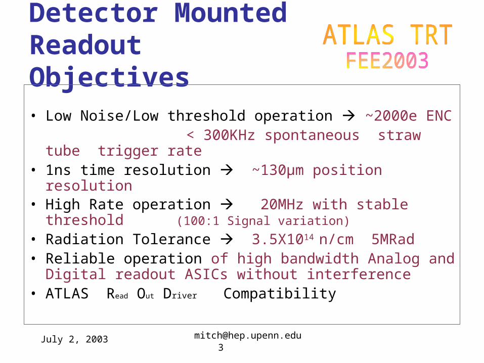
Detector Mounted Readout Objectives• Low Noise/Low threshold operation ~2000e ENC < 300KHz spontaneous straw tube trigger rate • 1ns time resolution ~130µm position resolution• High Rate operation 20MHz with stable threshold
(100:1 Signal variation)
• Radiation Tolerance 3.5X10¹⁴ n/cm 5MRad• Reliable operation of high bandwidth Analog and Digital
readout ASICs without interference• ATLAS Read Out Driver Compatibility


July 2, 2003 [email protected]
ASDBLR References
Implementation of the ASDBLR Straw Tube Readout ASIC in DMILL Technology
N. Dressnandt, N. Lam, F.M. Newcomer, R. Van Berg and H.H. Williams
IEEE (2000) Trans. On Nucl. Sci. V48 n4 p1239
An Amplifier-Shaper-Discriminator with Baseline Restoration for the ATLAS Transition Radiation Tracker B. Bevensee, F.M. Newcomer, R. P. Van Berg and H.H. Williams
IEEE (1996) Trans. on Nuc. Sci. V 43 p1725
http://www.hep.upenn.edu/atlas

July 2, 2003 [email protected]
ASDBLR 8 Ch Analog Front End
DTMROC
Differential Signal Processing
Tracking Comparator Input gain ~18mV/fC
Track Threshold Gain ~ 120mV/fC TR Threshold Gain ~ 10mV/fC
July 2, 2003 [email protected]
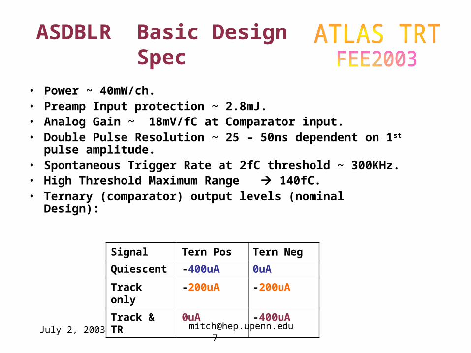
ASDBLR Basic Design Spec
• Power ~ 40mW/ch.• Preamp Input protection ~ 2.8mJ. • Analog Gain ~ 18mV/fC at Comparator input.• Double Pulse Resolution ~ 25 – 50ns dependent on 1st
pulse amplitude.• Spontaneous Trigger Rate at 2fC threshold ~ 300KHz.• High Threshold Maximum Range 140fC.• Ternary (comparator) output levels (nominal Design):
Signal Tern Pos Tern Neg
Quiescent -400uA 0uA
Track only -200uA -200uA
Track & TR 0uA -400uA
July 2, 2003 [email protected]
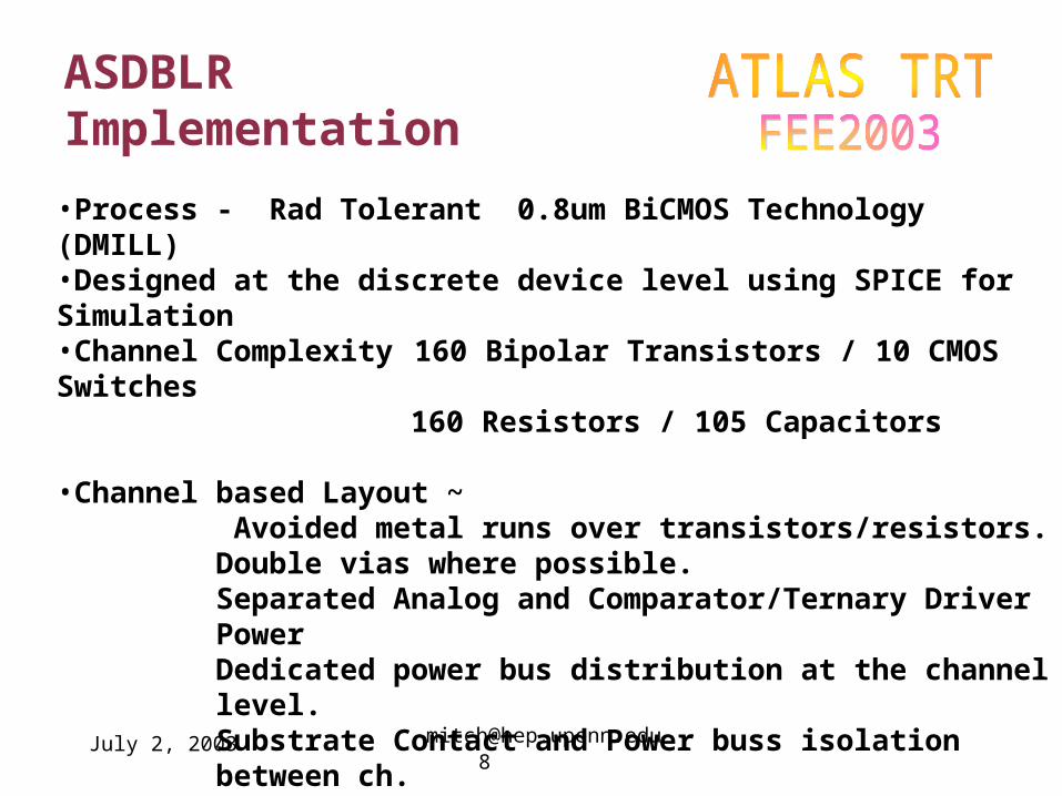
ASDBLR Implementation
•Process - Rad Tolerant 0.8um BiCMOS Technology (DMILL)•Designed at the discrete device level using SPICE for Simulation•Channel Complexity 160 Bipolar Transistors / 10 CMOS Switches
160 Resistors / 105 Capacitors
•Channel based Layout ~ Avoided metal runs over transistors/resistors.
Double vias where possible.Separated Analog and Comparator/Ternary Driver PowerDedicated power bus distribution at the channel level. Substrate Contact and Power buss isolation between ch.Preamp Supply filter on each channel.
•Eight (nearly) identical Channels on 340um Pitch
July 2, 2003 [email protected]
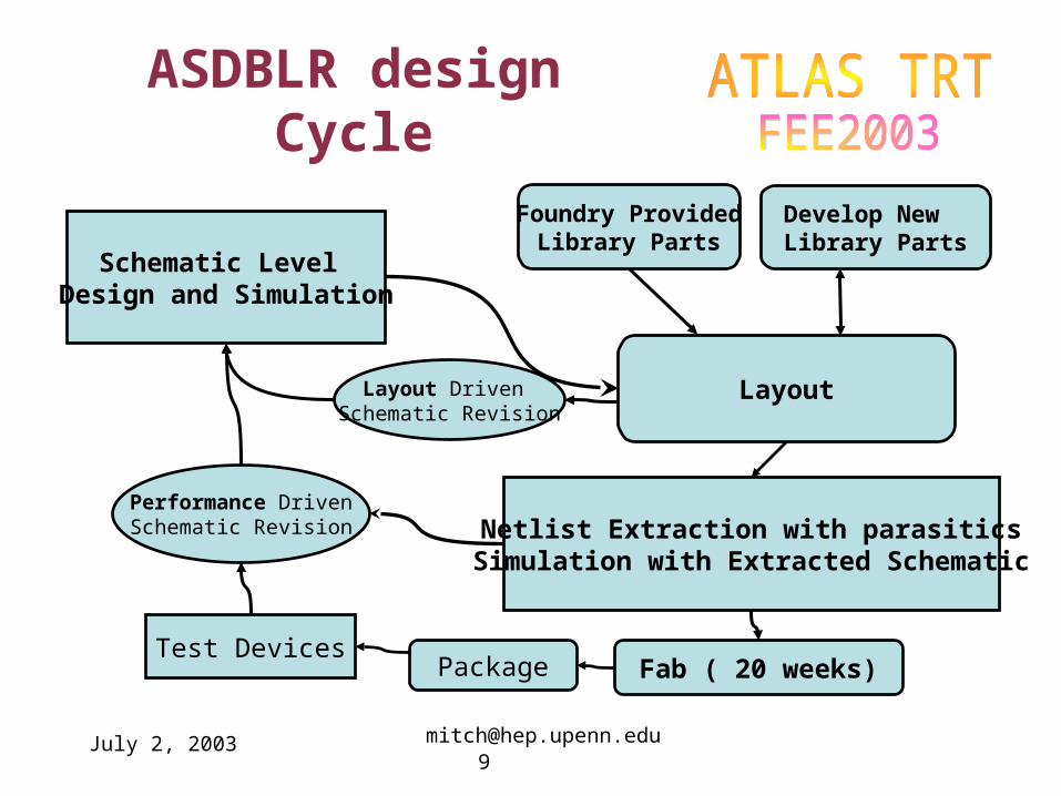
ASDBLR design Cycle
Layout
Netlist Extraction with parasiticsSimulation with Extracted Schematic
Layout Driven Schematic Revision
Foundry ProvidedLibrary Parts
Develop New Library Parts
Performance Driven Schematic Revision
Fab ( 20 weeks) Test Devices
Package
Schematic Level Design and Simulation

July 2, 2003 [email protected]
ASDBLR02 Final Design
• Reduce area of input protection network Reduce Capacitance 11pf 5pF.
• Increase Input transistor current to 7.5uA/m reduce beta loss.
• Increase analog gain by 50% to reduce sensitivity to device matching in comparator. (56mV/fC at BLR output)
Final Design Improvements
• Input referred threshold matching good, RMS < .25fC• Noise ~ 2100e ENC on board with ~5pF capacitance (100e/pf).• Power ~ 40mW/channel.• High Rate operation ~ demonstrated to 20MHz (pulser tests)
Measured Results

July 2, 2003 [email protected]
Production ASDBLR
Dual Preamps intermingled
layout
Input Transistors in
cross Quad Configuration
Input protection NPN Transistors
Expanded GeometryEmitter Stripes 4 x 30 um
3.3 X 3.6mm
Comparators
B L R’s
Shapers
Preamps

July 2, 2003 [email protected]
ASDBLR Radiation Testing
• Gamma Testing up to 7MRad with no significant performance degradation.
• 1MeV NEIL Neutron Testing to 5X10¹⁴ (10 year with saftey factor) shows a significant reduction in beta resulting in lower gain and increasing the channel to channel threshold offset. At Beta = 30 the gain is lowered by ~ 50%. – DMILL NPN Beta is sensitive to Thermal
Neutrons More study needed. Moderator re-evaluation?

July 2, 2003 [email protected]
Neutrons
Thermal Neutrons present at the Ljubjana facility point out a possible weakness using the DMILL Process.
Careful comparison of these results with the expected exposure in the ATLAS ID need to be performed.
8 year TRT Exposure
with Safety factors
All devices annealed at 150o C for 48 hrs.
(1MeV NEIL)

July 2, 2003 [email protected]
ASDBLR Radiation Testing
report NSS 2002
AS
DB
LR
# ch
ips
Po
wer o
n
Date
Type Dose1
Ch
ang
e in
Resistan
ce
Po
st Rad
N
PN
Beta
3 4/00 5X10¹³ n NA 84 3 4/00 1X10¹⁴ n NA 52 99
6 x 5/01 5Mrad 5% 180 00 9 10/01 3.5 X10¹⁴ n 1.5% 55 3
01 6 x 6/02 1.5X10 14 p 5% 70 01 16 x 7/02 7MRad 8% 130 01 10 5/02 3.5X10¹⁴ n 10.4% 11 2,3
1 n and p dose is in units of particles/cm2.
2 Thermal neutron dose high ~1014 n/cm2.3 After annealing 23hrs@150C
0
5
10
15
20
25
30
35
0.0 5.0 10.0 15.0 20.0 25.0 30.0 35.0
Collector Current Density (A/M)
Bet
a af
ter N
eutro
n D
amag
e
Average Values for 6 irradiated 4um NPN's
Input Transistor Track Disc Comparator
Shaper Stages
From: Radiation Hardness: Design Approach and Measurements of the ASDBLR ASIC for the ATLAS TRT
Nandor Dressnandt, Mitch Newcomer, member IEEE, Ole Rohne and Steven Passmore
See NSS 2002 Confrence Record
Summary of Device tests to 11 / 2002
The measured current gain of DMILL NPN transistors after exposure to 3.5X10¹⁴n/cm2 and prior to annealing. The arrows show the operating points chosen for various parts of the ASDBLR channel design. After annealing the beta
increased by a factor of two.
July 2, 2003 [email protected]
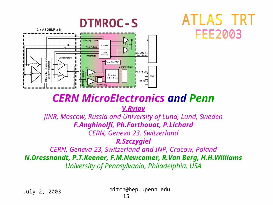
DTMROC-S
CERN MicroElectronics and PennV.Ryjov
JINR, Moscow, Russia and University of Lund, Lund, SwedenF.Anghinolfi, Ph.Farthouat, P.Lichard
CERN, Geneva 23, SwitzerlandR.Szczygiel
CERN, Geneva 23, Switzerland and INP, Cracow, PolandN.Dressnandt, P.T.Keener, F.M.Newcomer, R.Van Berg,
H.H.WilliamsUniversity of Pennsylvania, Philadelphia, USA
July 2, 2003 [email protected]
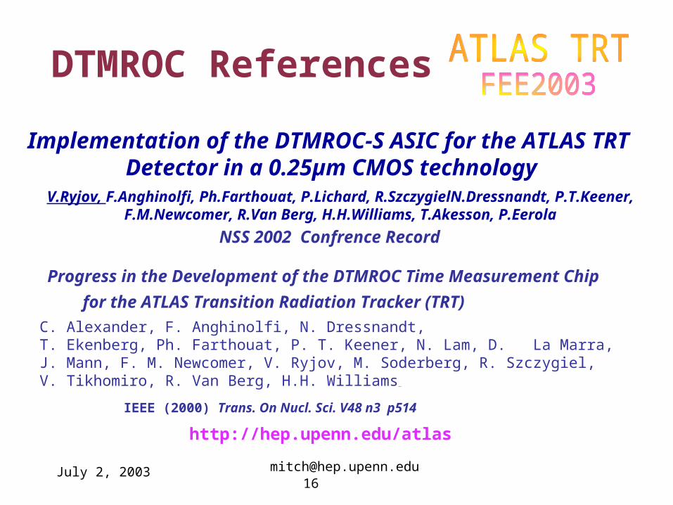
DTMROC References
Progress in the Development of the DTMROC Time Measurement Chip
for the ATLAS Transition Radiation Tracker (TRT)C. Alexander, F. Anghinolfi, N. Dressnandt, T. Ekenberg, Ph. Farthouat, P. T. Keener, N. Lam, D. La Marra, J. Mann, F. M. Newcomer, V. Ryjov, M. Soderberg, R. Szczygiel, V. Tikhomiro, R. Van Berg, H.H. Williams
IEEE (2000) Trans. On Nucl. Sci. V48 n3 p514
Implementation of the DTMROC-S ASIC for the ATLAS TRT Detector in a 0.25µm CMOS technology
V.Ryjov, F.Anghinolfi, Ph.Farthouat, P.Lichard, R.SzczygielN.Dressnandt, P.T.Keener, F.M.Newcomer, R.Van Berg, H.H.Williams, T.Akesson, P.Eerola
http://hep.upenn.edu/atlas
NSS 2002 Confrence Record


July 2, 2003 [email protected]
DTMROC–S Time Marking
• 8 equally spaced clock outputs used to sample straw track pulses
• 50% duty cycle clock regenerated to run the chip core logic
REF CLO CK
BC1
BC2
BC3
BC4
BC5
BC6
BC7
BC8
Lthr
00000011 11111110Frontend Latching Frontend Latching
In p ipeline la tch ing In p ipeline la tch ing
32 elements delay chain, phase detector, charge pump
40MHz Clock 3ns time bins


July 2, 2003 [email protected]
DTMROC–S
I/O
•Full/Reduced read-out : 444/380 bits per event, including Header
•LVDS-compatible, tristate drivers -> 40 Mbits/s copper links•Wire-OR” – for self triggering
fast-out option - selectedternary inputs contribute to the chip-level trigger
Up to 15 DTMROCs can be “OR’ed on a common buss

July 2, 2003 [email protected]
DTMROC-S DAC’s
• Internal bandgap reference 1.26V
• Current mirror master - 128 PMOS unit devices (L=8um,W=5um)
• 256 identical PMOS slave current mirrors per DAC
V.Ryjov

July 2, 2003 [email protected]
DTMROC-S Analog Sensing
• Two DACs• Four
Comparators– Temperature– VDD– Ext Voltage
1– Ext Voltage
2
Vdd Sense remained at 191 from 26 – 55 C

July 2, 2003 [email protected]
DTMROC-Stestability
• General-purpose 32-bits Status Register • Logical OR of all DTMROC error indicators in the Data
Header field• Parity check logic for all internal registers• Lock status, a “watch dog” and a “dynamic” check
circuitries examine the DLL• JTAG Boundary-Scan• Special scan mode - configures all DTMROC flip-flops
as a large shift register controlled via JTAG interface• Memory Build-In-Self-Test (BIST) controlled via the
Configuration register and JTAG interface

July 2, 2003 [email protected]
• Internal registers are equipped with parity error check
• The most critical parts arebuilt of the SEU resistantand self-recovering elementsbased on triple logic withmajority vote.
• Statistics circuit monitors the number of detected SEU’s
DTMROC-SSEU Protection
V.Ryjov

July 2, 2003 [email protected]
DTMROC-SDesign Tools(CERN based)
• Verilog modelling• Synopsys synthesis tools• Silicon Ensemble
Place&Route tools• Completely scripted physical
design flow• Number of synthesis-layout
cycles to predict post-route timing during RTL synthesis
• NC Verilog Simulator – Interleaved Native Compiled Code Architecture
BehavioralModel
Synopsyssynthesis
Place&
Route
Netlists
SynopsysLibrary
Compiler
HyperExtract LayoutWire Load
Table
Technology
Library
verilog
V.Ryjov


July 2, 2003 [email protected]
DTMROC-SFab
• Submitted/fabricated (.25um process) in Jan 2002– Wafer size 8” (350µm) → 1017 useable dies per wafer
• 850 chips tested on the mixed signal IMS Tester at CERN
• 5 process corner (85/92/100/115/125%) evaluated• 87% Yield for 850 chips• Irradiation tolerance test at CEA Saclay Pagure facility
in July 2002• SEU sensitivity evaluated at the CERN PS in July 2002• Test Beam at the CERN H8 in August-September 2002

July 2, 2003 [email protected]
DTMROC-SRadiation Testing
Total Ionizing Dose toleranceTotal Ionizing Dose tolerance• Tested at CEA Saclay Pagure facility in July 2002• 7 Mrad total dose / 1.33 MeV gamma radiation• ~10% increase in the DAC’s output voltage after irradiation, no
DNL change• No variations in the power consumption and the chip performance
SEU sensitivitySEU sensitivity• Evaluated at the CERN PS irradiation facility in July 2002• Integrated fluence of 1.81014p/cm2 on 24GeV beam• SEU cross-section for a single D flip-flop in different internal
registers varies from 0.810-14 to 1.210-14 cm2
• Impact of SEU’s in the vital components is suppressed by self-recovering logic

July 2, 2003 [email protected]
ASDBLR & DTMROC
Packaging Labeling
Fine Pitch Ball Grid ArraysLaser Marked packages2D Bar code
Human Readable numbering


July 2, 2003 [email protected]
IMS Tests on ASDBLR
Read Bar code and record test (event) Number
• Supply Current• Input voltage/resistance• Output current / switching• Low Threshold response to 0, 2, 3 fC input• High Threshold response to 30 fC. Write Results to SQL data base

July 2, 2003 [email protected]
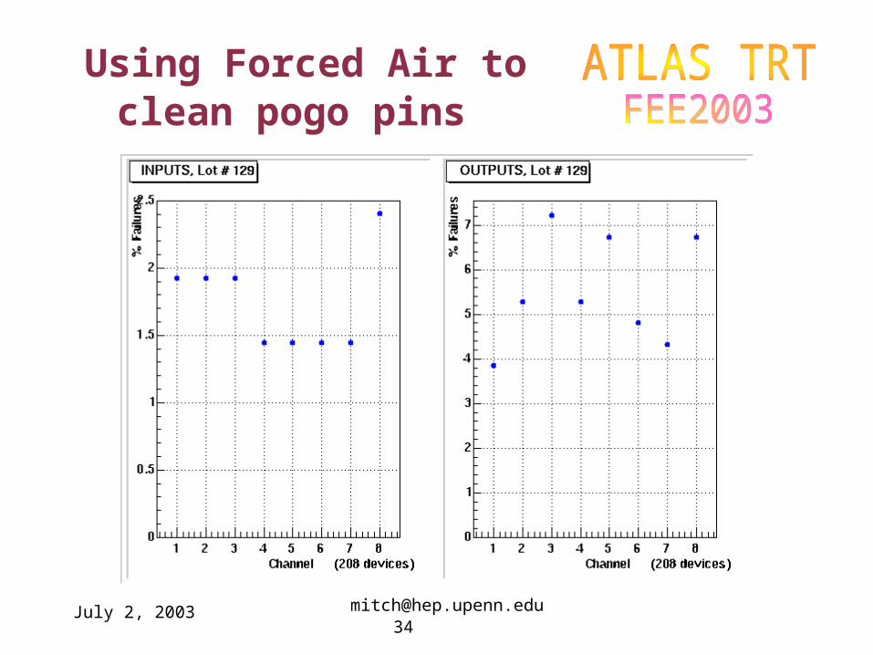
Failures Due to Socket Pin
Reliability
UnreliablePin ContactOn Output


July 2, 2003 [email protected]
IMS Beta Stage Testing Experience
• First 3000 chips demonstrate minor problems. • Socket Pins must be cleared with forced air
daily. • Some wandering of the Threshold 50% points
day to day.• Bar code too close to chip label, leads to ~5%
read errors. False failure rate ~10% presently Should improve over time.

July 2, 2003 [email protected]
Yield on First 3000 Devices with Beta
Testing version
Represents Yield of ASICS and Tester
Target for Final Acceptance

July 2, 2003 [email protected]
End Cap Wheel Boards
• 192 channels per assembly• 2 DTM Board’s = 1 virtual
module.– 1/32 of endcap type A
wheel• Flexible interconnect between
64 channel DTMROC boards allows 192 channel board to follow curvature of wheel tread.
• Initial noise measurements on prototype detector show operation at 2fC possible.
Side view of the stackup of one 64 channel ASD board, one (old) 64 channel DTM board, and a connector board
192 channel DTMROC board


July 2, 2003 [email protected]
Noise Rate Plot with Barrel ModuleBoard and
Pulser
6 MHz = 50% Pulser Efficiency(note that Pulser adds noise)

July 2, 2003 [email protected]
Analog and Digital Readout on the Barrel Module Board (good
Channel)
75ns
50% Efficiency Dac Setting by Time Bin
5mV/ Dac
~ 24 Counts/fC
Test
Pu
lse r
esp
on
se

July 2, 2003 [email protected]
Beating Down Pulser Noise
using DTMROC Timing window
50% Threshold VS Input Charge
0
50
100
150
200
250
0 1 2 3 4 5 6
Pulser input Charge in fC
DT
MR
OC
D
AC
co
un
ts
Full 75ns Time Window
12ns Time Window
24Cnts / fC140mV / fC

July 2, 2003 [email protected]
Test Beam Measurements
Spatial Resolution
S. Smirnov
100
140
Rate MHz2010

July 2, 2003 [email protected]
Test Beam Performance of Production ASICS and
near final prototype boards.
S. Smirnov

July 2, 2003 [email protected]
Summary
• ASDBLR and DTMROC ASICs are in production and have been shown to meet TRT design objectives.
• Development of Production ASIC Testing Facility is nearly finished.
• Design of Boards with both analog and digital ASICS on them is underway and we have very promising results to date.
• Radiation Testing of ASDBLR ASICS indicates npn neutron sensitivity that may limit lifetime to ~8 years when safety factors are considered.
• Thermal neutron content of TRT environment needs study.