the 8088 and 8086 microprocessors
DESCRIPTION
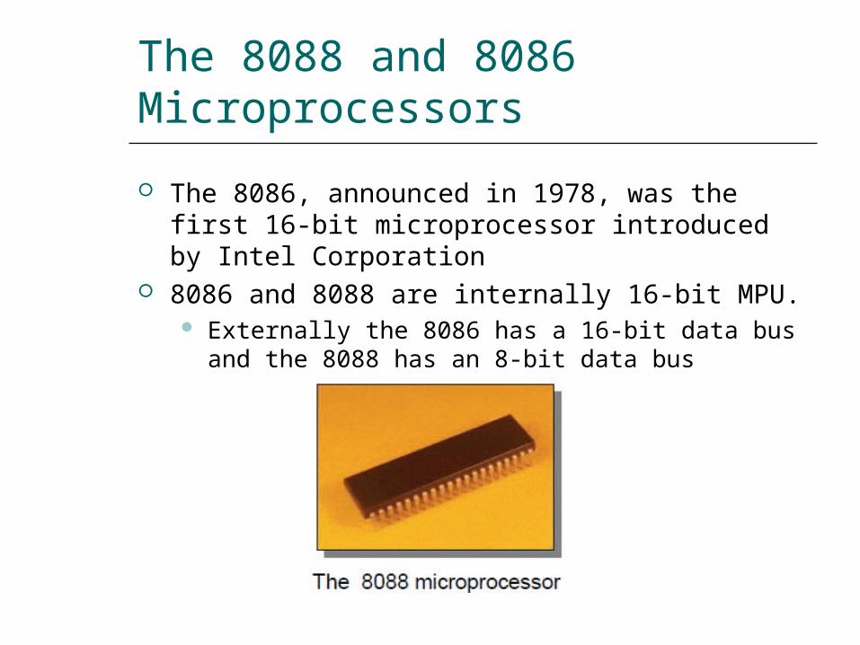
The 8088 and 8086 Microprocessors. The 8086, announced in 1978, was the first 16-bit microprocessor introduced by Intel Corporation 8086 and 8088 are internally 16-bit MPU. Externally the 8086 has a 16-bit data bus and the 8088 has an 8-bit data bus. The 8088 and 8086 Microprocessors (cont.). - PowerPoint PPT PresentationTRANSCRIPT
The 8088 and 8086 Microprocessors
The 8086 announced in 1978 was the first 16-bit microprocessor introduced by Intel Corporation
8086 and 8088 are internally 16-bit MPU Externally the 8086 has a 16-bit data bus and the
8088 has an 8-bit data bus
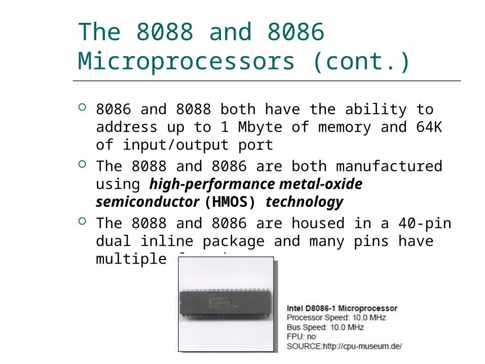
The 8088 and 8086 Microprocessors (cont)
8086 and 8088 both have the ability to address up to 1 Mbyte of memory and 64K of inputoutput port
The 8088 and 8086 are both manufactured using high-performance metal-oxide semiconductor (HMOS) technology
The 8088 and 8086 are housed in a 40-pin dual inline package and many pins have multiple functions
The 8088 and 8086 Microprocessors (cont)
CMOS Complementary Metal-Oxide-Semiconductor is a major class of integrated circuits used in chips such as microprocessors microcontrollers static RAM digital logic circuits and analog circuits such as image sensors
Two important characteristics of CMOS devices are high noise immunity and low static power supply drain
Significant power is only drawn when its transistors are switching between on and off states
The 8088 and 8086 Microprocessors (cont)
CMOS devices do not produce as much heat as other forms of logic such as TTL
CMOS also allows a high density of logic functions on a chip
The 8088 and 8086 Microprocessors (cont)
Pin layout of the 8086 and 8088 microprocessor
bull 16-bit Arithmetic Logic Unit
bull 16-bit data bus (8088 has 8-bit data bus)
bull 20-bit address bus - 220 = 1048576 = 1 meg
The address refers to a byte in memory In the 8088 these bytes come in on the 8-bit data bus In the 8086 bytes at even addresses come in on the low half of the data bus (bits 0-7) and bytes at odd addresses come in on the upper half of the data bus (bits 8-15)
The 8086 can read a 16-bit word at an even address in one operation and at an odd address in two operations The 8088 needs two operations in either case
The least significant byte of a word on an 8086 family microprocessor is at the lower address
8086 Features
Simplified CPU Design
Data Registers
Address Registers
ControlUnit
ArithmeticLogic Unit
StatusFlags
Address Bus
Data Bus
Memory
CS
SS
DS
ES
Segment
BP
Index
SP
SI
DI
AH
BH
CH
DH DL
CL
BL
AL
General Purpose
Status and Control
Flags
IP
AX
BX
CX
DX
Intel 16-bit Registers
bull The 8086 has two parts the Bus Interface Unit (BIU) and the Execution Unit (EU)
bull The BIU fetches instructions reads and writes data and computes the 20-bit address
bull The EU decodes and executes the instructions using the 16-bit ALU
bull The BIU contains the following registers
IP - the Instruction PointerCS - the Code Segment RegisterDS - the Data Segment RegisterSS - the Stack Segment RegisterES - the Extra Segment Register
The BIU fetches instructions using the CS and IP written CSIP to contract the 20-bit address Data is fetched using a segment register (usually the DS) and an effective address (EA) computed by the EU depending on the addressing mode
8086 Architecture
The EU contains the following 16-bit registers
AX - the AccumulatorBX - the Base RegisterCX - the Count RegisterDX - the Data Register
SP - the Stack Pointer defaults to stack segment
BP - the Base Pointer SI - the Source Index RegisterDI - the Destination Register
These are referred to as general-purpose registers although as seen by their names they often have a special-purpose use for some instructions
The AX BX CX and DX registers can be considers as two 8-bit registers a High byte and a Low byte This allows byte operations and compatibility with the previous generation of 8-bit processors the 8080 and 8085 8085 source code could be translated in 8086 code and assembled The 8-bit registers are
AX --gt AHALBX --gt BHBLCX --gt CHCLDX --gt DHDL
8086 Programmerrsquos Model
ESCSSSDSIP
AHBHCHDH
ALBLCLDL
SPBP
SIDI
FLAGS
AXBX
CX
DX
Extra SegmentCode Segment
Stack SegmentData SegmentInstruction Pointer
Accumulator
Base RegisterCount RegisterData RegisterStack PointerBase PointerSource Index RegisterDestination Index Register
BIU registers
(20 bit adder)
EU registers
808688 internal registers 16 bits (2 bytes each)808688 internal registers 16 bits (2 bytes each)
AX BX CX and DX are twobytes wide and each byte can
be accessed separately
These registers are used as memory pointers
Flags will be discussed later
Segment registers are usedas base address for a segment
in the 1 M byte of memory
The 80868088 Microprocessors Registers
bull Registers
ndash Registers are in the CPU and are referred to by specific names
ndash Data registersbull Hold data for an operation to be performed bull There are 4 data registers (AX BX CX DX)
ndash Address registersbull Hold the address of an instruction or data elementbull Segment registers (CS DS ES SS)bull Pointer registers (SP BP IP)bull Index registers (SI DI)
ndash Status registerbull Keeps the current status of the processor bull On an IBM PC the status register is called the FLAGS
register
ndash In total there are fourteen 16-bit registers in an 80868088
Data Registers AX BX CX DX
bull Instructions execute faster if the data is in a registerbull AX BX CX DX are the data registersbull Low and High bytes of the data registers can be accessed
separately
ndash AH BH CH DH are the high bytesndash AL BL CL and DL are the low bytes
bull Data Registers are general purpose registers but they also perform special functions
bull AX
ndash Accumulator Register ndash Preferred register to use in arithmetic logic and data
transfer instructions because it generates the shortest Machine Language Code
ndash Must be used in multiplication and division operationsndash Must also be used in IO operations
bull BX
ndash Base Registerndash Also serves as an address registerndash Used in array operationsndash Used in Table Lookup operations (XLAT)
bull CX
ndash Count registerndash Used as a loop counterndash Used in shift and rotate operations
bull DX
ndash Data registerndash Used in multiplication and divisionndash Also used in IO operations
Pointer and Index Registers
bull Contain the offset addresses of memory locationsbull Can also be used in arithmetic and other operationsbull SP Stack pointer
ndash Used with SS to access the stack segmentbull BP Base Pointer
ndash Primarily used to access data on the stackndash Can be used to access data in other segments
bull SI Source Index register
ndash is required for some string operationsndash When string operations are performed the SI
register points to memory locations in the data segment which is addressed by the DS register Thus SI is associated with the DS in string operations
bull DI Destination Index register ndash is also required for some string operations
ndash When string operations are performed the DI register points to memory locations in the data segment which is addressed by the ES register Thus DI is associated with the ES in string
operationsbull The SI and the DI registers may also be used to access data
stored in arrays
Segment Registers - CS DS SS and ES
bull Are Address registersbull Store the memory addresses of instructions and databull Memory Organization
ndash Each byte in memory has a 20 bit address starting with 0 to 220-1 or 1 meg of addressable memory
ndash Addresses are expressed as 5 hex digits from 00000 - FFFFF
ndash Problem But 20 bit addresses are TOO BIG to fit in 16 bit registers
ndash Solution Memory Segmentbull Block of 64K (65536) consecutive memory bytesbull A segment number is a 16 bit numberbull Segment numbers range from 0000 to FFFFbull Within a segment a particular memory location is specified
with an offsetbull An offset also ranges from 0000 to FFFF
Segmented MemorySegmented memory addressing absolute (linear) address is a combination of a 16-bit segment value added to a 16-bit offset
li ne
ar a
ddre
sse
s
one segment
Memory Address Generation
Memory Address Generation
bull The BIU has a dedicated adder for determining physical memory addresses
Intel
Physical Address (20 Bits)
Adder
Segment Register (16 bits) 0 0 0 0
Offset Value (16 bits)
Example Address Calculation
Example Address Calculation
bull If the data segment starts at location 1000h and a data reference contains the address 29h where is the actual data
Intel
Offset 0 0 0 0 0 0 0 0 0 0 1 0 1 0 0 1
2 9
0 0 0 1 0 0 0 0 0 0 0 0 0 0 0 0 0 0 0 0Segment
0 0 0 1 0 0 0 0 0 0 0 0 0 0 1 0 1 0 0 1Address
SegmentOffset Address
bull Logical Address is specified as segmentoffsetbull Physical address is obtained by shifting the segment address 4
bits to the left and adding the offset addressbull Thus the physical address of the logical address A4FB4872 is
A4FB0+ 4872 A9822
Your turn
What linear address corresponds to the segmentoffset address 028F0030
028F0 + 0030 = 02920
Always use hexadecimal notation for addresses
Your turn
What segment addresses correspond to the linear address 28F30h
Many different segment-offset addresses can produce the linear address 28F30h For example
28F00030 28F30000 28B00430
The Code Segment
Memory
Segment Register
Offset
Physical orAbsolute Address
0
+
CS
IP
0400H
0056H
4000H
4056H
0400
0056
04056H
The offset is the distance in bytes from the start of the segmentThe offset is given by the IP for the Code SegmentInstructions are always fetched with using the CS register
CSIP = 40056Logical Address
0H
0FFFFFH
The physical address is also called the absolute address
The Data Segment
Memory
Segment Register
Offset
Physical Address
+
DS
EA
05C0
0050
05C00H
05C50H
05C0 0
0050
05C50H
Data is usually fetched with respect to the DS registerThe effective address (EA) is the offsetThe EA depends on the addressing mode
DSEA
0H
0FFFFFH
The Stack Segment
Memory
Segment Register
Offset
Physical Address
+
SS
SP
0A00
0100
0A000H
0A100H
0A00 0
0100
0A100H
The stack is always referenced with respect to the stack segment registerThe stack grows toward decreasing memory locationsThe SP points to the last or top item on the stack
PUSH - pre-decrement the SPPOP - post-increment the SP
The offset is given by the SP register
SSSP
0H
0FFFFFH
FlagsFlags
Carry flag
Parity flag
Auxiliary flag
Zero
Overflow
Direction
Interrupt enable
Trap
Sign6 are status flags3 are control flag
bull CF (carry) Contains carry from leftmost bit following arithmetic also contains last bit from a shift or rotate operation
Flag Register
Flag O D I T S Z A P C
Bit no 15 14 13 12 1110
9 8 7 6 5 4 3 2 1 0
bull Conditional flags ndash They are set according to some results of arithmetic
operation You do not need to alter the value yourselfbull Control flags
ndash Used to control some operations of the MPU These flags are to be set by you in order to achieve some specific
purposes
Flag Register
bull OF (overflow) Indicates overflow of the leftmost bit during arithmetic
bull DF (direction) Indicates left or right for moving or comparing string data
bull IF (interrupt) Indicates whether external interrupts are being processed or ignored
bull TF (trap) Permits operation of the processor in single step mode
bull SF (sign) Contains the resulting sign of an arithmetic operation (1=negative)
bull ZF (zero) Indicates when the result of arithmetic or a comparison is zero (1=yes)
bull AF (auxiliary carry) Contains carry out of bit 3 into bit 4 for specialized arithmetic
bull PF (parity) Indicates the number of 1 bits that result from an operation
Minimum-Mode and Maximum-Mode System
Minimum-Mode and Maximum-Mode System (cont)
Signals common to both minimum and maximum mode
Minimum-Mode and Maximum-Mode System (cont)
Unique minimum-mode signals
Minimum-Mode and Maximum-Mode System (cont)
Unique maximum-mode signals
Minimum-Mode and Maximum-Mode System (cont)
Minimum-Mode Interface
Block diagram of the minimum-mode 8088 MPU
Minimum-Mode Interface (cont)
Block diagram of the minimum-mode 8086 MPU
Minimum-Mode Interface (cont)
The minimum-mode signals can be divided into the following basic groups AddressData bus Status signals Control signals Interrupt signals DMA interface signals
Minimum-Mode Interface (cont)
AddressData bus The address bus is used to carry address information to
the memory and IO ports The address bus is 20-bit long and consists of signal lines
A0 through A19
A 20-bit address gives the 8088 a 1 Mbyte memory address space
Only address line A0 through A15 are used when addressing IO
This give an IO address space of 64 Kbytes The 8088 has 8 multiplexed addressdata bus lines
(A0~A7)
8086 has 16 multiplexed addressdata bus lines (A0~A15)
Minimum-Mode Interface (cont)
Status signals The four most significant address A19 through A16
are multiplexed with status signal S6 through S3
Bits S4 and S3 together form a 2-bit binary code that identifies which of the internal segment registers was used to generate the physical address
S5 is the logic level of the internal interrupt flag S6 is always at the 0 logic level
Minimum-Mode Interface (cont)
Minimum-Mode Interface (cont)
Minimum-Mode Interface (cont)
Maximum-Mode Interface
The maximum-mode configuration is mainly used for implementing a multiprocessorcoprocessor system environment Multiple processors exist in the system Each executes its own program
Global resources and local resources The former are common to all processors The latter are assigned to specific processors
In the maximum-mode facilities are provided for implementing allocation of global resources and passing bus control to other microprocessors sharing the system bus
Maximum-Mode Interface (cont)
8088 maximum-mode block diagram
Maximum-Mode Interface (cont)
8086 maximum-mode block diagram
Maximum-Mode Interface (cont)
8288 bus controller
Block diagram and pin layout of 8288
Maximum-Mode Interface (cont)
8288 bus controller In the maximum-mode 80888086 outputs a
status code on three signal line S0 S1 S2 prior to the initialization of each bus cycle
The 3-bit bus status code identifies which type of bus cycle is to follow and are input to the external bus controller device 8288
The 8288 produces one or two command signals for each bus cycle
Maximum-Mode Interface (cont)
8288 bus controller
Bus status code
Maximum-Mode Interface (cont)
Maximum-Mode Interface (cont)
Maximum-Mode Interface (cont)
Queue status signals The 2-bit queue status code QS0 and QS1 tells
the external circuitry what type of information was removed form the queue during the previous clock cycle
Queue status code
Electrical Characteristics
Power is applied between pin 40 (Vcc) and pins 1 (GND) and 20 (GND)
The nominal value of Vcc is specified as +5V dc with a tolerance of plusmn10
Both 8088 and 8086 draw a maximum of 340mA from the supply
IO voltage levels
System Clock
The time base for synchronization of the internal and external operations of the microprocessor in a microcomputer system is provided by the clock (CLK) input signal The standard 8088 operates at 5 MHz and the
8088-2 operates at 8 MHz The 8086 is manufactured in three speeds 5-
MHz 8086 8-MHz 8086-2 and the 10-MHz 8086-1
The CLK is externally generated by the 8284 clock generator and driver IC
System Clock (cont)
Block diagram of the 8284 clock generator
System Clock (cont)
Block diagram of the 8284 clock generator
System Clock (cont)
Connecting the 8284 to the 8088
15- or 24MHzcrystal
Typical value of CL when used with 15MHz crystal is 12pF
The fundamental crystal frequency is divided by 3 within the 8284 to give either a 5- or 8-MHz clock signal
System Clock (cont)
CLK waveform The signal is specified at Metal Oxide
Semiconductor (MOS)-compatible voltage level The period of the 5-MHz 8088 can range from
200 ns to 500 ns and the maximum rise and fall times of its edges equal 10 ns
System Clock (cont)
PCLK and OSC signals The peripheral clock (PCLK) and oscillator clock
(OSC) signals are provided to drive peripheral ICs The clock output at PCLK is half the frequency of
CLK The OSC output is at the crystal frequency which is three times of CLK
System Clock (cont)
The 8284 can also be driven from an external clock source Applied to the EFI (External Frequency Input) Input FC is used for selection
0 crystal between X1 and X2 is used 1 selects EFI
The CSYNC input is used for external synchronization in systems with multiple clocks
System Clock (cont)
EXAMPLE If the CLK input of an 8086 MPU is to be driven by
a 9-MHz signal what speed version of the 8086 must be used and what frequency crystal must be attached to the 8284
Solution The 8086-1 is the version of the 8086 that can be
run at 9-MHz To create the 9-MHz clock a 27-MHz crystal must be used on the 8284
Bus Cycle and Time States
A bus cycle defines the basic operation that a microprocessor performs to communicate with external devices
Examples of bus cycles are the memory read memory write inputoutput read and inputoutput write
The bus cycle of the 8088 and 8086 microprocessors consists of at least four clock periods
If no bus cycles are required the microprocessor performs what are known as idle states
When READY is held at the 0 level wait states are inserted between states T3 and T4 of the bus cycle
Bus Cycle and Time States (cont)
Bus cycle clock periods idle state and wait state
Bus Cycle and Time States (cont)
EXAMPLE What is the duration of the bus cycle in the 8088-
based microcomputer if the clock is 8 MHz and the two wait states are inserted
Solution The duration of the bus cycle in an 8 MHz system
is given by tcyc = 500 ns + N x 125 ns
In this expression the N stands for the number of waits states For a bus cycle with two wait states we get
tcyc = 500 ns + 2 x 125 ns = 500 ns + 250 ns = 750 ns
Hardware Organization of the Memory Address Space
1Mx8 memory bank of the 8088
Hardware Organization of the Memory Address Space (cont)
High and low memory banks of the 8086
Hardware Organization of the Memory Address Space (cont)
Byte transfer by the 8088
Hardware Organization of the Memory Address Space (cont)
Word transfer by the 8088
Hardware Organization of the Memory Address Space (cont)
Even address byte transfer by the 8086
Hardware Organization of the Memory Address Space (cont)
Odd address byte transfer by the 8086
Hardware Organization of the Memory Address Space (cont)
Even address word transfer by the 8086
Hardware Organization of the Memory Address Space (cont)
Odd-address word transfer by the 8086
Hardware Organization of the Memory Address Space (cont)
EXAMPLE Is the word at memory address 0123116 of an
8086-based microcomputer aligned or misaligned How many cycle are required to read it from memory
Solution The first byte of the word is the second byte at
the aligned-word address 0123016 Therefore the word is misaligned and required two bus cycles to be read from memory
Address Bus Status Codes
Whenever a memory bus cycle is in progress an address bus status code S4S3 is output by the processor S4S3 identifies which one of the four segment
register is used to generate the physical address in the current bus cycle 1048729
S4S3=00 identifies the extra segment register (ES)
S4S3=01 identifies the stack segment register (SS)
S4S3=10 identifies the code segment register (CS)
S4S3=11 identifies the data segment register (DS)
The memory address reach of the microprocessor can thus be expanded to 4 Mbytes
Memory Control Signals
Minimum-mode memory control signals
Memory Control Signals (cont)
Minimum-mode memory control signals (8088) ALE ndash Address Latch Enable ndash used to latch
the address in external memory IOM ndash Input-OutputMemory ndash signal external
circuitry whether a memory of IO bus cycle is in progress
DTR ndash Data TransmitReceive ndash signal external circuitry whether the 8088 is transmitting or receiving data over the bus 1048729
RD ndash Read ndash identifies that a read bus cycle is in progress
WR ndash Write ndash identifies that a write bus cycle is in progress
DEN ndash Data Enable ndash used to enable the data bus 1048729
SSO ndash Status Line ndash identifies whether a code or data access is in progress
Memory Control Signals (cont)
The control signals for the 8086rsquos minimum-mode memory interface differs in three ways IOM signal is replaced by MIO signal The signal SSO is removed from the interface BHE (bank high enable) is added to the interface
and is used to select input for the high bank of memory in the 8086rsquos memory subsystem
Memory Control Signals (cont)
Maximum-mode memory control signals
Memory Control Signals (cont)
Maximum-mode memory control signals MRDC ndash Memory Read Command 1048729 MWTC ndash Memory Write Command 1048729 AMWC ndash Advanced Memory Write Command
Read and Write Bus Cycle
Read cycle
Minimum-mode memory read bus cycle of the 8088
Read and Write Bus Cycle (cont)
Read cycle
Minimum-mode memory read bus cycle of the 8086
Read and Write Bus Cycle (cont)
Read cycle
Maximum-mode memory read bus cycle of the 8086
Read and Write Bus Cycle (cont)
Write cycle
Minimum-mode memory write bus cycle of the 8088
Read and Write Bus Cycle (cont)
Write cycle
Maximum-mode memory write bus cycle of the 8086
Memory Interface Circuit
Address bus latches and buffers Bank write and bank read control logic Data bus transceiversbuffers Address decoders
Memory Interface Circuit (cont)
Memory interface block diagram
Memory Interface Circuit (cont)
Address bus latches and buffers
Block diagram of a D-type latch
Memory Interface Circuit (cont)
Address bus latches and buffers
Circuit diagram of the 74F373
Memory Interface Circuit (cont)
A review of flip-floplatch logic
Positive edge-triggered D flip-flop
Memory Interface Circuit (cont)
A review of flip-floplatch logic
Positive edge-triggered JK flip-flop
Memory Interface Circuit (cont)
A review of flip-floplatch logic
D-type latch
Memory Interface Circuit (cont)
Address bus latches and buffers
Address latch circuit
Memory Interface Circuit (cont)
Bank write and bank read control logic
Bank write control logic Bank read control logic
Memory Interface Circuit (cont)
Data bus transceivers
Block diagram and circuit diagram of the 74F245 octal bus transceiver
Memory Interface Circuit (cont)
Data bus transceivers
Data bus transceiver circuit
Memory Interface Circuit (cont)
Address decoder
Address bus configuration with address decoding
Memory Interface Circuit (cont)
Address decoder
Block diagram and operation of the 74F139 decoder
Memory Interface Circuit (cont)
Address decoder
Circuit diagram of the 74F139 decoder
Memory Interface Circuit (cont)
Address decoder
Address decoder circuit using 74F139
Memory Interface Circuit (cont)
Address decoder
Block diagram and operation of the 74F138 decoder
Memory Interface Circuit (cont)
Address decoder
Circuit diagram of the 74F138 decoder
Memory Interface Circuit (cont)
Address decoder
Address decoder circuit using 74F138
Types of InputOutput
The IO system allows peripherals to provide data or receive results of processing the data Using IO ports
The 80888086 MPU can employ two types of IO Isolated IO Memory-mapped IO
They differ in how IO ports are mapped into the address space
Types of InputOutput (cont)
Isolated inputoutput When using isolated IO in a microcomputer
system the IO device are treated separate from memory
The memory address space contains 1 M consecutive byte address in the range 0000016 through FFFFF16
The IO address space contains 64K consecutive byte addresses in the range 000016 through FFFF16
The bytes in two consecutive IO addresses can be accessed as word-wide data
Page 0 000016 00FF16
Certain IO instructions can only perform in this range
Types of InputOutput (cont)
Isolated inputoutput
80888086 memory and IO address spaces
Types of InputOutput (cont)
Isolated inputoutput
Isolated IO ports
Types of InputOutput (cont)
Isolated inputoutput Advantages
The complete 1Mbyte memory address space is available for use with memory
Special instructions have been provided to perform IO operations with maximized performance
The bytes in two consecutive IO addresses can be accessed as word-wide data
Disadvantages All input and output data transfers must take place
between the AL or AX register and IO port
Types of InputOutput (cont)
Memory-mapped inputoutput MPU looks at the IO port as though it is a storage
location in memory Some of the memory address space is dedicated to IO
ports Instructions that affect data in memory are used
instead of the special IO instructions More instructions and addressing modes are available to
perform IO operations IO transfers can take place between IO port and other
internal registers The memory instructions tend to execute slower
than those specifically designed for isolated IO Part of the memory address space is lost
Types of InputOutput(cont)
Memory-mapped inputoutput
Memory mapped IO ports
Isolated InputOutput Interface
IO devices Keyboard Printer Mouse 82C55A etc
Functions of interface circuit Select the IO port Latch output data Sample input data Synchronize data transfer Translate between TTL voltage levels and those
required to operate the IO devices
Isolated InputOutput Interface (cont)
Minimum-mode interface
Minimum-mode 8088 system IO interface
Isolated InputOutput Interface (cont)
Minimum-mode interface
Minimum-mode 8086 system IO interface
Isolated InputOutput Interface (cont)
Maximum-mode interface
Maximum-mode 8088 system IO interface
Isolated InputOutput Interface (cont)
Maximum-mode interface
Maximum-mode 8086 system IO interface
Isolated InputOutput Interface (cont)
Maximum-mode interface
IO bus cycle status codes
InputOutput Data Transfer
Inputoutput data transfers in the 8088 and 8086 microcomputers can be either byte-wide or word-wide
IO addresses are 16 bits in length and are output by the 8088 to the IO interface over bus lines AD0 through AD7 and A8 through A15
In 8088 the word transfers is performed as two consecutive byte-wide data transfer and takes two bus cycle
In 8086 the word transfers can takes either one or two bus cycle
Word-wide IO ports should be aligned at even-address boundaries
InputOutput Data Instructions
InputOutput Data Instructions(cont)
EXAMPLE Write a sequence of instructions that will output
the data FF16 to a byte-wide output port at address AB16 of the IO address space
Solution First the AL register is loaded with FF16 as an
immediate operand in the instruction
MOV AL 0FFH Now the data in AL can be output to the byte-
wide output port with the instruction
OUT 0ABH AL
InputOutput Data Instructions(cont)
EXAMPLE Write a series of instructions that will output FF16 to an
output port located at address B00016 of the IO address space
Solution The DX register must first be loaded with the address
of the output port This is done with the instructionMOV DX 0B000H
Next the data that are to be output must be loaded into AL with the instruction
MOV AL 0FFH Finally the data are output with the instruction
OUT DX AL
InputOutput Data Instructions(cont)
EXAMPLE Data are to be read in from two byte-wide input
ports at addresses AA16 and A916 and then output as a word-wide output port at address B00016 Write a sequence of instructions to perform this inputoutput operation
InputOutput Data Instructions(cont)
Solution First read in the byte at address AA16 into AL and
move it into AHIN AL 0AAHMOV AH AL
Now the other byte can be read into AL by the instructionIN AL 09AH
And to write out the word of dataMOV DX 0B000HOUT DX AX
InputOutput Bus Cycles
Input bus cycle of the 8088
InputOutput Bus Cycles (cont)
Output bus cycle of the 8088
InputOutput Bus Cycles (cont)
Input bus cycle of the 8086
InputOutput Bus Cycles (cont)
Output bus cycle of the 8086
The 8088 and 8086 Microprocessors (cont)
Pin layout of the 8086 and 8088 microprocessor
bull 16-bit Arithmetic Logic Unit
bull 16-bit data bus (8088 has 8-bit data bus)
bull 20-bit address bus - 220 = 1048576 = 1 meg
The address refers to a byte in memory In the 8088 these bytes come in on the 8-bit data bus In the 8086 bytes at even addresses come in on the low half of the data bus (bits 0-7) and bytes at odd addresses come in on the upper half of the data bus (bits 8-15)
The 8086 can read a 16-bit word at an even address in one operation and at an odd address in two operations The 8088 needs two operations in either case
The least significant byte of a word on an 8086 family microprocessor is at the lower address
8086 Features
Simplified CPU Design
Data Registers
Address Registers
ControlUnit
ArithmeticLogic Unit
StatusFlags
Address Bus
Data Bus
Memory
CS
SS
DS
ES
Segment
BP
Index
SP
SI
DI
AH
BH
CH
DH DL
CL
BL
AL
General Purpose
Status and Control
Flags
IP
AX
BX
CX
DX
Intel 16-bit Registers
bull The 8086 has two parts the Bus Interface Unit (BIU) and the Execution Unit (EU)
bull The BIU fetches instructions reads and writes data and computes the 20-bit address
bull The EU decodes and executes the instructions using the 16-bit ALU
bull The BIU contains the following registers
IP - the Instruction PointerCS - the Code Segment RegisterDS - the Data Segment RegisterSS - the Stack Segment RegisterES - the Extra Segment Register
The BIU fetches instructions using the CS and IP written CSIP to contract the 20-bit address Data is fetched using a segment register (usually the DS) and an effective address (EA) computed by the EU depending on the addressing mode
8086 Architecture
The EU contains the following 16-bit registers
AX - the AccumulatorBX - the Base RegisterCX - the Count RegisterDX - the Data Register
SP - the Stack Pointer defaults to stack segment
BP - the Base Pointer SI - the Source Index RegisterDI - the Destination Register
These are referred to as general-purpose registers although as seen by their names they often have a special-purpose use for some instructions
The AX BX CX and DX registers can be considers as two 8-bit registers a High byte and a Low byte This allows byte operations and compatibility with the previous generation of 8-bit processors the 8080 and 8085 8085 source code could be translated in 8086 code and assembled The 8-bit registers are
AX --gt AHALBX --gt BHBLCX --gt CHCLDX --gt DHDL
8086 Programmerrsquos Model
ESCSSSDSIP
AHBHCHDH
ALBLCLDL
SPBP
SIDI
FLAGS
AXBX
CX
DX
Extra SegmentCode Segment
Stack SegmentData SegmentInstruction Pointer
Accumulator
Base RegisterCount RegisterData RegisterStack PointerBase PointerSource Index RegisterDestination Index Register
BIU registers
(20 bit adder)
EU registers
808688 internal registers 16 bits (2 bytes each)808688 internal registers 16 bits (2 bytes each)
AX BX CX and DX are twobytes wide and each byte can
be accessed separately
These registers are used as memory pointers
Flags will be discussed later
Segment registers are usedas base address for a segment
in the 1 M byte of memory
The 80868088 Microprocessors Registers
bull Registers
ndash Registers are in the CPU and are referred to by specific names
ndash Data registersbull Hold data for an operation to be performed bull There are 4 data registers (AX BX CX DX)
ndash Address registersbull Hold the address of an instruction or data elementbull Segment registers (CS DS ES SS)bull Pointer registers (SP BP IP)bull Index registers (SI DI)
ndash Status registerbull Keeps the current status of the processor bull On an IBM PC the status register is called the FLAGS
register
ndash In total there are fourteen 16-bit registers in an 80868088
Data Registers AX BX CX DX
bull Instructions execute faster if the data is in a registerbull AX BX CX DX are the data registersbull Low and High bytes of the data registers can be accessed
separately
ndash AH BH CH DH are the high bytesndash AL BL CL and DL are the low bytes
bull Data Registers are general purpose registers but they also perform special functions
bull AX
ndash Accumulator Register ndash Preferred register to use in arithmetic logic and data
transfer instructions because it generates the shortest Machine Language Code
ndash Must be used in multiplication and division operationsndash Must also be used in IO operations
bull BX
ndash Base Registerndash Also serves as an address registerndash Used in array operationsndash Used in Table Lookup operations (XLAT)
bull CX
ndash Count registerndash Used as a loop counterndash Used in shift and rotate operations
bull DX
ndash Data registerndash Used in multiplication and divisionndash Also used in IO operations
Pointer and Index Registers
bull Contain the offset addresses of memory locationsbull Can also be used in arithmetic and other operationsbull SP Stack pointer
ndash Used with SS to access the stack segmentbull BP Base Pointer
ndash Primarily used to access data on the stackndash Can be used to access data in other segments
bull SI Source Index register
ndash is required for some string operationsndash When string operations are performed the SI
register points to memory locations in the data segment which is addressed by the DS register Thus SI is associated with the DS in string operations
bull DI Destination Index register ndash is also required for some string operations
ndash When string operations are performed the DI register points to memory locations in the data segment which is addressed by the ES register Thus DI is associated with the ES in string
operationsbull The SI and the DI registers may also be used to access data
stored in arrays
Segment Registers - CS DS SS and ES
bull Are Address registersbull Store the memory addresses of instructions and databull Memory Organization
ndash Each byte in memory has a 20 bit address starting with 0 to 220-1 or 1 meg of addressable memory
ndash Addresses are expressed as 5 hex digits from 00000 - FFFFF
ndash Problem But 20 bit addresses are TOO BIG to fit in 16 bit registers
ndash Solution Memory Segmentbull Block of 64K (65536) consecutive memory bytesbull A segment number is a 16 bit numberbull Segment numbers range from 0000 to FFFFbull Within a segment a particular memory location is specified
with an offsetbull An offset also ranges from 0000 to FFFF
Segmented MemorySegmented memory addressing absolute (linear) address is a combination of a 16-bit segment value added to a 16-bit offset
li ne
ar a
ddre
sse
s
one segment
Memory Address Generation
Memory Address Generation
bull The BIU has a dedicated adder for determining physical memory addresses
Intel
Physical Address (20 Bits)
Adder
Segment Register (16 bits) 0 0 0 0
Offset Value (16 bits)
Example Address Calculation
Example Address Calculation
bull If the data segment starts at location 1000h and a data reference contains the address 29h where is the actual data
Intel
Offset 0 0 0 0 0 0 0 0 0 0 1 0 1 0 0 1
2 9
0 0 0 1 0 0 0 0 0 0 0 0 0 0 0 0 0 0 0 0Segment
0 0 0 1 0 0 0 0 0 0 0 0 0 0 1 0 1 0 0 1Address
SegmentOffset Address
bull Logical Address is specified as segmentoffsetbull Physical address is obtained by shifting the segment address 4
bits to the left and adding the offset addressbull Thus the physical address of the logical address A4FB4872 is
A4FB0+ 4872 A9822
Your turn
What linear address corresponds to the segmentoffset address 028F0030
028F0 + 0030 = 02920
Always use hexadecimal notation for addresses
Your turn
What segment addresses correspond to the linear address 28F30h
Many different segment-offset addresses can produce the linear address 28F30h For example
28F00030 28F30000 28B00430
The Code Segment
Memory
Segment Register
Offset
Physical orAbsolute Address
0
+
CS
IP
0400H
0056H
4000H
4056H
0400
0056
04056H
The offset is the distance in bytes from the start of the segmentThe offset is given by the IP for the Code SegmentInstructions are always fetched with using the CS register
CSIP = 40056Logical Address
0H
0FFFFFH
The physical address is also called the absolute address
The Data Segment
Memory
Segment Register
Offset
Physical Address
+
DS
EA
05C0
0050
05C00H
05C50H
05C0 0
0050
05C50H
Data is usually fetched with respect to the DS registerThe effective address (EA) is the offsetThe EA depends on the addressing mode
DSEA
0H
0FFFFFH
The Stack Segment
Memory
Segment Register
Offset
Physical Address
+
SS
SP
0A00
0100
0A000H
0A100H
0A00 0
0100
0A100H
The stack is always referenced with respect to the stack segment registerThe stack grows toward decreasing memory locationsThe SP points to the last or top item on the stack
PUSH - pre-decrement the SPPOP - post-increment the SP
The offset is given by the SP register
SSSP
0H
0FFFFFH
FlagsFlags
Carry flag
Parity flag
Auxiliary flag
Zero
Overflow
Direction
Interrupt enable
Trap
Sign6 are status flags3 are control flag
bull CF (carry) Contains carry from leftmost bit following arithmetic also contains last bit from a shift or rotate operation
Flag Register
Flag O D I T S Z A P C
Bit no 15 14 13 12 1110
9 8 7 6 5 4 3 2 1 0
bull Conditional flags ndash They are set according to some results of arithmetic
operation You do not need to alter the value yourselfbull Control flags
ndash Used to control some operations of the MPU These flags are to be set by you in order to achieve some specific
purposes
Flag Register
bull OF (overflow) Indicates overflow of the leftmost bit during arithmetic
bull DF (direction) Indicates left or right for moving or comparing string data
bull IF (interrupt) Indicates whether external interrupts are being processed or ignored
bull TF (trap) Permits operation of the processor in single step mode
bull SF (sign) Contains the resulting sign of an arithmetic operation (1=negative)
bull ZF (zero) Indicates when the result of arithmetic or a comparison is zero (1=yes)
bull AF (auxiliary carry) Contains carry out of bit 3 into bit 4 for specialized arithmetic
bull PF (parity) Indicates the number of 1 bits that result from an operation
Minimum-Mode and Maximum-Mode System
Minimum-Mode and Maximum-Mode System (cont)
Signals common to both minimum and maximum mode
Minimum-Mode and Maximum-Mode System (cont)
Unique minimum-mode signals
Minimum-Mode and Maximum-Mode System (cont)
Unique maximum-mode signals
Minimum-Mode and Maximum-Mode System (cont)
Minimum-Mode Interface
Block diagram of the minimum-mode 8088 MPU
Minimum-Mode Interface (cont)
Block diagram of the minimum-mode 8086 MPU
Minimum-Mode Interface (cont)
The minimum-mode signals can be divided into the following basic groups AddressData bus Status signals Control signals Interrupt signals DMA interface signals
Minimum-Mode Interface (cont)
AddressData bus The address bus is used to carry address information to
the memory and IO ports The address bus is 20-bit long and consists of signal lines
A0 through A19
A 20-bit address gives the 8088 a 1 Mbyte memory address space
Only address line A0 through A15 are used when addressing IO
This give an IO address space of 64 Kbytes The 8088 has 8 multiplexed addressdata bus lines
(A0~A7)
8086 has 16 multiplexed addressdata bus lines (A0~A15)
Minimum-Mode Interface (cont)
Status signals The four most significant address A19 through A16
are multiplexed with status signal S6 through S3
Bits S4 and S3 together form a 2-bit binary code that identifies which of the internal segment registers was used to generate the physical address
S5 is the logic level of the internal interrupt flag S6 is always at the 0 logic level
Minimum-Mode Interface (cont)
Minimum-Mode Interface (cont)
Minimum-Mode Interface (cont)
Maximum-Mode Interface
The maximum-mode configuration is mainly used for implementing a multiprocessorcoprocessor system environment Multiple processors exist in the system Each executes its own program
Global resources and local resources The former are common to all processors The latter are assigned to specific processors
In the maximum-mode facilities are provided for implementing allocation of global resources and passing bus control to other microprocessors sharing the system bus
Maximum-Mode Interface (cont)
8088 maximum-mode block diagram
Maximum-Mode Interface (cont)
8086 maximum-mode block diagram
Maximum-Mode Interface (cont)
8288 bus controller
Block diagram and pin layout of 8288
Maximum-Mode Interface (cont)
8288 bus controller In the maximum-mode 80888086 outputs a
status code on three signal line S0 S1 S2 prior to the initialization of each bus cycle
The 3-bit bus status code identifies which type of bus cycle is to follow and are input to the external bus controller device 8288
The 8288 produces one or two command signals for each bus cycle
Maximum-Mode Interface (cont)
8288 bus controller
Bus status code
Maximum-Mode Interface (cont)
Maximum-Mode Interface (cont)
Maximum-Mode Interface (cont)
Queue status signals The 2-bit queue status code QS0 and QS1 tells
the external circuitry what type of information was removed form the queue during the previous clock cycle
Queue status code
Electrical Characteristics
Power is applied between pin 40 (Vcc) and pins 1 (GND) and 20 (GND)
The nominal value of Vcc is specified as +5V dc with a tolerance of plusmn10
Both 8088 and 8086 draw a maximum of 340mA from the supply
IO voltage levels
System Clock
The time base for synchronization of the internal and external operations of the microprocessor in a microcomputer system is provided by the clock (CLK) input signal The standard 8088 operates at 5 MHz and the
8088-2 operates at 8 MHz The 8086 is manufactured in three speeds 5-
MHz 8086 8-MHz 8086-2 and the 10-MHz 8086-1
The CLK is externally generated by the 8284 clock generator and driver IC
System Clock (cont)
Block diagram of the 8284 clock generator
System Clock (cont)
Block diagram of the 8284 clock generator
System Clock (cont)
Connecting the 8284 to the 8088
15- or 24MHzcrystal
Typical value of CL when used with 15MHz crystal is 12pF
The fundamental crystal frequency is divided by 3 within the 8284 to give either a 5- or 8-MHz clock signal
System Clock (cont)
CLK waveform The signal is specified at Metal Oxide
Semiconductor (MOS)-compatible voltage level The period of the 5-MHz 8088 can range from
200 ns to 500 ns and the maximum rise and fall times of its edges equal 10 ns
System Clock (cont)
PCLK and OSC signals The peripheral clock (PCLK) and oscillator clock
(OSC) signals are provided to drive peripheral ICs The clock output at PCLK is half the frequency of
CLK The OSC output is at the crystal frequency which is three times of CLK
System Clock (cont)
The 8284 can also be driven from an external clock source Applied to the EFI (External Frequency Input) Input FC is used for selection
0 crystal between X1 and X2 is used 1 selects EFI
The CSYNC input is used for external synchronization in systems with multiple clocks
System Clock (cont)
EXAMPLE If the CLK input of an 8086 MPU is to be driven by
a 9-MHz signal what speed version of the 8086 must be used and what frequency crystal must be attached to the 8284
Solution The 8086-1 is the version of the 8086 that can be
run at 9-MHz To create the 9-MHz clock a 27-MHz crystal must be used on the 8284
Bus Cycle and Time States
A bus cycle defines the basic operation that a microprocessor performs to communicate with external devices
Examples of bus cycles are the memory read memory write inputoutput read and inputoutput write
The bus cycle of the 8088 and 8086 microprocessors consists of at least four clock periods
If no bus cycles are required the microprocessor performs what are known as idle states
When READY is held at the 0 level wait states are inserted between states T3 and T4 of the bus cycle
Bus Cycle and Time States (cont)
Bus cycle clock periods idle state and wait state
Bus Cycle and Time States (cont)
EXAMPLE What is the duration of the bus cycle in the 8088-
based microcomputer if the clock is 8 MHz and the two wait states are inserted
Solution The duration of the bus cycle in an 8 MHz system
is given by tcyc = 500 ns + N x 125 ns
In this expression the N stands for the number of waits states For a bus cycle with two wait states we get
tcyc = 500 ns + 2 x 125 ns = 500 ns + 250 ns = 750 ns
Hardware Organization of the Memory Address Space
1Mx8 memory bank of the 8088
Hardware Organization of the Memory Address Space (cont)
High and low memory banks of the 8086
Hardware Organization of the Memory Address Space (cont)
Byte transfer by the 8088
Hardware Organization of the Memory Address Space (cont)
Word transfer by the 8088
Hardware Organization of the Memory Address Space (cont)
Even address byte transfer by the 8086
Hardware Organization of the Memory Address Space (cont)
Odd address byte transfer by the 8086
Hardware Organization of the Memory Address Space (cont)
Even address word transfer by the 8086
Hardware Organization of the Memory Address Space (cont)
Odd-address word transfer by the 8086
Hardware Organization of the Memory Address Space (cont)
EXAMPLE Is the word at memory address 0123116 of an
8086-based microcomputer aligned or misaligned How many cycle are required to read it from memory
Solution The first byte of the word is the second byte at
the aligned-word address 0123016 Therefore the word is misaligned and required two bus cycles to be read from memory
Address Bus Status Codes
Whenever a memory bus cycle is in progress an address bus status code S4S3 is output by the processor S4S3 identifies which one of the four segment
register is used to generate the physical address in the current bus cycle 1048729
S4S3=00 identifies the extra segment register (ES)
S4S3=01 identifies the stack segment register (SS)
S4S3=10 identifies the code segment register (CS)
S4S3=11 identifies the data segment register (DS)
The memory address reach of the microprocessor can thus be expanded to 4 Mbytes
Memory Control Signals
Minimum-mode memory control signals
Memory Control Signals (cont)
Minimum-mode memory control signals (8088) ALE ndash Address Latch Enable ndash used to latch
the address in external memory IOM ndash Input-OutputMemory ndash signal external
circuitry whether a memory of IO bus cycle is in progress
DTR ndash Data TransmitReceive ndash signal external circuitry whether the 8088 is transmitting or receiving data over the bus 1048729
RD ndash Read ndash identifies that a read bus cycle is in progress
WR ndash Write ndash identifies that a write bus cycle is in progress
DEN ndash Data Enable ndash used to enable the data bus 1048729
SSO ndash Status Line ndash identifies whether a code or data access is in progress
Memory Control Signals (cont)
The control signals for the 8086rsquos minimum-mode memory interface differs in three ways IOM signal is replaced by MIO signal The signal SSO is removed from the interface BHE (bank high enable) is added to the interface
and is used to select input for the high bank of memory in the 8086rsquos memory subsystem
Memory Control Signals (cont)
Maximum-mode memory control signals
Memory Control Signals (cont)
Maximum-mode memory control signals MRDC ndash Memory Read Command 1048729 MWTC ndash Memory Write Command 1048729 AMWC ndash Advanced Memory Write Command
Read and Write Bus Cycle
Read cycle
Minimum-mode memory read bus cycle of the 8088
Read and Write Bus Cycle (cont)
Read cycle
Minimum-mode memory read bus cycle of the 8086
Read and Write Bus Cycle (cont)
Read cycle
Maximum-mode memory read bus cycle of the 8086
Read and Write Bus Cycle (cont)
Write cycle
Minimum-mode memory write bus cycle of the 8088
Read and Write Bus Cycle (cont)
Write cycle
Maximum-mode memory write bus cycle of the 8086
Memory Interface Circuit
Address bus latches and buffers Bank write and bank read control logic Data bus transceiversbuffers Address decoders
Memory Interface Circuit (cont)
Memory interface block diagram
Memory Interface Circuit (cont)
Address bus latches and buffers
Block diagram of a D-type latch
Memory Interface Circuit (cont)
Address bus latches and buffers
Circuit diagram of the 74F373
Memory Interface Circuit (cont)
A review of flip-floplatch logic
Positive edge-triggered D flip-flop
Memory Interface Circuit (cont)
A review of flip-floplatch logic
Positive edge-triggered JK flip-flop
Memory Interface Circuit (cont)
A review of flip-floplatch logic
D-type latch
Memory Interface Circuit (cont)
Address bus latches and buffers
Address latch circuit
Memory Interface Circuit (cont)
Bank write and bank read control logic
Bank write control logic Bank read control logic
Memory Interface Circuit (cont)
Data bus transceivers
Block diagram and circuit diagram of the 74F245 octal bus transceiver
Memory Interface Circuit (cont)
Data bus transceivers
Data bus transceiver circuit
Memory Interface Circuit (cont)
Address decoder
Address bus configuration with address decoding
Memory Interface Circuit (cont)
Address decoder
Block diagram and operation of the 74F139 decoder
Memory Interface Circuit (cont)
Address decoder
Circuit diagram of the 74F139 decoder
Memory Interface Circuit (cont)
Address decoder
Address decoder circuit using 74F139
Memory Interface Circuit (cont)
Address decoder
Block diagram and operation of the 74F138 decoder
Memory Interface Circuit (cont)
Address decoder
Circuit diagram of the 74F138 decoder
Memory Interface Circuit (cont)
Address decoder
Address decoder circuit using 74F138
Types of InputOutput
The IO system allows peripherals to provide data or receive results of processing the data Using IO ports
The 80888086 MPU can employ two types of IO Isolated IO Memory-mapped IO
They differ in how IO ports are mapped into the address space
Types of InputOutput (cont)
Isolated inputoutput When using isolated IO in a microcomputer
system the IO device are treated separate from memory
The memory address space contains 1 M consecutive byte address in the range 0000016 through FFFFF16
The IO address space contains 64K consecutive byte addresses in the range 000016 through FFFF16
The bytes in two consecutive IO addresses can be accessed as word-wide data
Page 0 000016 00FF16
Certain IO instructions can only perform in this range
Types of InputOutput (cont)
Isolated inputoutput
80888086 memory and IO address spaces
Types of InputOutput (cont)
Isolated inputoutput
Isolated IO ports
Types of InputOutput (cont)
Isolated inputoutput Advantages
The complete 1Mbyte memory address space is available for use with memory
Special instructions have been provided to perform IO operations with maximized performance
The bytes in two consecutive IO addresses can be accessed as word-wide data
Disadvantages All input and output data transfers must take place
between the AL or AX register and IO port
Types of InputOutput (cont)
Memory-mapped inputoutput MPU looks at the IO port as though it is a storage
location in memory Some of the memory address space is dedicated to IO
ports Instructions that affect data in memory are used
instead of the special IO instructions More instructions and addressing modes are available to
perform IO operations IO transfers can take place between IO port and other
internal registers The memory instructions tend to execute slower
than those specifically designed for isolated IO Part of the memory address space is lost
Types of InputOutput(cont)
Memory-mapped inputoutput
Memory mapped IO ports
Isolated InputOutput Interface
IO devices Keyboard Printer Mouse 82C55A etc
Functions of interface circuit Select the IO port Latch output data Sample input data Synchronize data transfer Translate between TTL voltage levels and those
required to operate the IO devices
Isolated InputOutput Interface (cont)
Minimum-mode interface
Minimum-mode 8088 system IO interface
Isolated InputOutput Interface (cont)
Minimum-mode interface
Minimum-mode 8086 system IO interface
Isolated InputOutput Interface (cont)
Maximum-mode interface
Maximum-mode 8088 system IO interface
Isolated InputOutput Interface (cont)
Maximum-mode interface
Maximum-mode 8086 system IO interface
Isolated InputOutput Interface (cont)
Maximum-mode interface
IO bus cycle status codes
InputOutput Data Transfer
Inputoutput data transfers in the 8088 and 8086 microcomputers can be either byte-wide or word-wide
IO addresses are 16 bits in length and are output by the 8088 to the IO interface over bus lines AD0 through AD7 and A8 through A15
In 8088 the word transfers is performed as two consecutive byte-wide data transfer and takes two bus cycle
In 8086 the word transfers can takes either one or two bus cycle
Word-wide IO ports should be aligned at even-address boundaries
InputOutput Data Instructions
InputOutput Data Instructions(cont)
EXAMPLE Write a sequence of instructions that will output
the data FF16 to a byte-wide output port at address AB16 of the IO address space
Solution First the AL register is loaded with FF16 as an
immediate operand in the instruction
MOV AL 0FFH Now the data in AL can be output to the byte-
wide output port with the instruction
OUT 0ABH AL
InputOutput Data Instructions(cont)
EXAMPLE Write a series of instructions that will output FF16 to an
output port located at address B00016 of the IO address space
Solution The DX register must first be loaded with the address
of the output port This is done with the instructionMOV DX 0B000H
Next the data that are to be output must be loaded into AL with the instruction
MOV AL 0FFH Finally the data are output with the instruction
OUT DX AL
InputOutput Data Instructions(cont)
EXAMPLE Data are to be read in from two byte-wide input
ports at addresses AA16 and A916 and then output as a word-wide output port at address B00016 Write a sequence of instructions to perform this inputoutput operation
InputOutput Data Instructions(cont)
Solution First read in the byte at address AA16 into AL and
move it into AHIN AL 0AAHMOV AH AL
Now the other byte can be read into AL by the instructionIN AL 09AH
And to write out the word of dataMOV DX 0B000HOUT DX AX
InputOutput Bus Cycles
Input bus cycle of the 8088
InputOutput Bus Cycles (cont)
Output bus cycle of the 8088
InputOutput Bus Cycles (cont)
Input bus cycle of the 8086
InputOutput Bus Cycles (cont)
Output bus cycle of the 8086
CS
SS
DS
ES
Segment
BP
Index
SP
SI
DI
AH
BH
CH
DH DL
CL
BL
AL
General Purpose
Status and Control
Flags
IP
AX
BX
CX
DX
Intel 16-bit Registers
bull The 8086 has two parts the Bus Interface Unit (BIU) and the Execution Unit (EU)
bull The BIU fetches instructions reads and writes data and computes the 20-bit address
bull The EU decodes and executes the instructions using the 16-bit ALU
bull The BIU contains the following registers
IP - the Instruction PointerCS - the Code Segment RegisterDS - the Data Segment RegisterSS - the Stack Segment RegisterES - the Extra Segment Register
The BIU fetches instructions using the CS and IP written CSIP to contract the 20-bit address Data is fetched using a segment register (usually the DS) and an effective address (EA) computed by the EU depending on the addressing mode
8086 Architecture
The EU contains the following 16-bit registers
AX - the AccumulatorBX - the Base RegisterCX - the Count RegisterDX - the Data Register
SP - the Stack Pointer defaults to stack segment
BP - the Base Pointer SI - the Source Index RegisterDI - the Destination Register
These are referred to as general-purpose registers although as seen by their names they often have a special-purpose use for some instructions
The AX BX CX and DX registers can be considers as two 8-bit registers a High byte and a Low byte This allows byte operations and compatibility with the previous generation of 8-bit processors the 8080 and 8085 8085 source code could be translated in 8086 code and assembled The 8-bit registers are
AX --gt AHALBX --gt BHBLCX --gt CHCLDX --gt DHDL
8086 Programmerrsquos Model
ESCSSSDSIP
AHBHCHDH
ALBLCLDL
SPBP
SIDI
FLAGS
AXBX
CX
DX
Extra SegmentCode Segment
Stack SegmentData SegmentInstruction Pointer
Accumulator
Base RegisterCount RegisterData RegisterStack PointerBase PointerSource Index RegisterDestination Index Register
BIU registers
(20 bit adder)
EU registers
808688 internal registers 16 bits (2 bytes each)808688 internal registers 16 bits (2 bytes each)
AX BX CX and DX are twobytes wide and each byte can
be accessed separately
These registers are used as memory pointers
Flags will be discussed later
Segment registers are usedas base address for a segment
in the 1 M byte of memory
The 80868088 Microprocessors Registers
bull Registers
ndash Registers are in the CPU and are referred to by specific names
ndash Data registersbull Hold data for an operation to be performed bull There are 4 data registers (AX BX CX DX)
ndash Address registersbull Hold the address of an instruction or data elementbull Segment registers (CS DS ES SS)bull Pointer registers (SP BP IP)bull Index registers (SI DI)
ndash Status registerbull Keeps the current status of the processor bull On an IBM PC the status register is called the FLAGS
register
ndash In total there are fourteen 16-bit registers in an 80868088
Data Registers AX BX CX DX
bull Instructions execute faster if the data is in a registerbull AX BX CX DX are the data registersbull Low and High bytes of the data registers can be accessed
separately
ndash AH BH CH DH are the high bytesndash AL BL CL and DL are the low bytes
bull Data Registers are general purpose registers but they also perform special functions
bull AX
ndash Accumulator Register ndash Preferred register to use in arithmetic logic and data
transfer instructions because it generates the shortest Machine Language Code
ndash Must be used in multiplication and division operationsndash Must also be used in IO operations
bull BX
ndash Base Registerndash Also serves as an address registerndash Used in array operationsndash Used in Table Lookup operations (XLAT)
bull CX
ndash Count registerndash Used as a loop counterndash Used in shift and rotate operations
bull DX
ndash Data registerndash Used in multiplication and divisionndash Also used in IO operations
Pointer and Index Registers
bull Contain the offset addresses of memory locationsbull Can also be used in arithmetic and other operationsbull SP Stack pointer
ndash Used with SS to access the stack segmentbull BP Base Pointer
ndash Primarily used to access data on the stackndash Can be used to access data in other segments
bull SI Source Index register
ndash is required for some string operationsndash When string operations are performed the SI
register points to memory locations in the data segment which is addressed by the DS register Thus SI is associated with the DS in string operations
bull DI Destination Index register ndash is also required for some string operations
ndash When string operations are performed the DI register points to memory locations in the data segment which is addressed by the ES register Thus DI is associated with the ES in string
operationsbull The SI and the DI registers may also be used to access data
stored in arrays
Segment Registers - CS DS SS and ES
bull Are Address registersbull Store the memory addresses of instructions and databull Memory Organization
ndash Each byte in memory has a 20 bit address starting with 0 to 220-1 or 1 meg of addressable memory
ndash Addresses are expressed as 5 hex digits from 00000 - FFFFF
ndash Problem But 20 bit addresses are TOO BIG to fit in 16 bit registers
ndash Solution Memory Segmentbull Block of 64K (65536) consecutive memory bytesbull A segment number is a 16 bit numberbull Segment numbers range from 0000 to FFFFbull Within a segment a particular memory location is specified
with an offsetbull An offset also ranges from 0000 to FFFF
Segmented MemorySegmented memory addressing absolute (linear) address is a combination of a 16-bit segment value added to a 16-bit offset
li ne
ar a
ddre
sse
s
one segment
Memory Address Generation
Memory Address Generation
bull The BIU has a dedicated adder for determining physical memory addresses
Intel
Physical Address (20 Bits)
Adder
Segment Register (16 bits) 0 0 0 0
Offset Value (16 bits)
Example Address Calculation
Example Address Calculation
bull If the data segment starts at location 1000h and a data reference contains the address 29h where is the actual data
Intel
Offset 0 0 0 0 0 0 0 0 0 0 1 0 1 0 0 1
2 9
0 0 0 1 0 0 0 0 0 0 0 0 0 0 0 0 0 0 0 0Segment
0 0 0 1 0 0 0 0 0 0 0 0 0 0 1 0 1 0 0 1Address
SegmentOffset Address
bull Logical Address is specified as segmentoffsetbull Physical address is obtained by shifting the segment address 4
bits to the left and adding the offset addressbull Thus the physical address of the logical address A4FB4872 is
A4FB0+ 4872 A9822
Your turn
What linear address corresponds to the segmentoffset address 028F0030
028F0 + 0030 = 02920
Always use hexadecimal notation for addresses
Your turn
What segment addresses correspond to the linear address 28F30h
Many different segment-offset addresses can produce the linear address 28F30h For example
28F00030 28F30000 28B00430
The Code Segment
Memory
Segment Register
Offset
Physical orAbsolute Address
0
+
CS
IP
0400H
0056H
4000H
4056H
0400
0056
04056H
The offset is the distance in bytes from the start of the segmentThe offset is given by the IP for the Code SegmentInstructions are always fetched with using the CS register
CSIP = 40056Logical Address
0H
0FFFFFH
The physical address is also called the absolute address
The Data Segment
Memory
Segment Register
Offset
Physical Address
+
DS
EA
05C0
0050
05C00H
05C50H
05C0 0
0050
05C50H
Data is usually fetched with respect to the DS registerThe effective address (EA) is the offsetThe EA depends on the addressing mode
DSEA
0H
0FFFFFH
The Stack Segment
Memory
Segment Register
Offset
Physical Address
+
SS
SP
0A00
0100
0A000H
0A100H
0A00 0
0100
0A100H
The stack is always referenced with respect to the stack segment registerThe stack grows toward decreasing memory locationsThe SP points to the last or top item on the stack
PUSH - pre-decrement the SPPOP - post-increment the SP
The offset is given by the SP register
SSSP
0H
0FFFFFH
FlagsFlags
Carry flag
Parity flag
Auxiliary flag
Zero
Overflow
Direction
Interrupt enable
Trap
Sign6 are status flags3 are control flag
bull CF (carry) Contains carry from leftmost bit following arithmetic also contains last bit from a shift or rotate operation
Flag Register
Flag O D I T S Z A P C
Bit no 15 14 13 12 1110
9 8 7 6 5 4 3 2 1 0
bull Conditional flags ndash They are set according to some results of arithmetic
operation You do not need to alter the value yourselfbull Control flags
ndash Used to control some operations of the MPU These flags are to be set by you in order to achieve some specific
purposes
Flag Register
bull OF (overflow) Indicates overflow of the leftmost bit during arithmetic
bull DF (direction) Indicates left or right for moving or comparing string data
bull IF (interrupt) Indicates whether external interrupts are being processed or ignored
bull TF (trap) Permits operation of the processor in single step mode
bull SF (sign) Contains the resulting sign of an arithmetic operation (1=negative)
bull ZF (zero) Indicates when the result of arithmetic or a comparison is zero (1=yes)
bull AF (auxiliary carry) Contains carry out of bit 3 into bit 4 for specialized arithmetic
bull PF (parity) Indicates the number of 1 bits that result from an operation
Minimum-Mode and Maximum-Mode System
Minimum-Mode and Maximum-Mode System (cont)
Signals common to both minimum and maximum mode
Minimum-Mode and Maximum-Mode System (cont)
Unique minimum-mode signals
Minimum-Mode and Maximum-Mode System (cont)
Unique maximum-mode signals
Minimum-Mode and Maximum-Mode System (cont)
Minimum-Mode Interface
Block diagram of the minimum-mode 8088 MPU
Minimum-Mode Interface (cont)
Block diagram of the minimum-mode 8086 MPU
Minimum-Mode Interface (cont)
The minimum-mode signals can be divided into the following basic groups AddressData bus Status signals Control signals Interrupt signals DMA interface signals
Minimum-Mode Interface (cont)
AddressData bus The address bus is used to carry address information to
the memory and IO ports The address bus is 20-bit long and consists of signal lines
A0 through A19
A 20-bit address gives the 8088 a 1 Mbyte memory address space
Only address line A0 through A15 are used when addressing IO
This give an IO address space of 64 Kbytes The 8088 has 8 multiplexed addressdata bus lines
(A0~A7)
8086 has 16 multiplexed addressdata bus lines (A0~A15)
Minimum-Mode Interface (cont)
Status signals The four most significant address A19 through A16
are multiplexed with status signal S6 through S3
Bits S4 and S3 together form a 2-bit binary code that identifies which of the internal segment registers was used to generate the physical address
S5 is the logic level of the internal interrupt flag S6 is always at the 0 logic level
Minimum-Mode Interface (cont)
Minimum-Mode Interface (cont)
Minimum-Mode Interface (cont)
Maximum-Mode Interface
The maximum-mode configuration is mainly used for implementing a multiprocessorcoprocessor system environment Multiple processors exist in the system Each executes its own program
Global resources and local resources The former are common to all processors The latter are assigned to specific processors
In the maximum-mode facilities are provided for implementing allocation of global resources and passing bus control to other microprocessors sharing the system bus
Maximum-Mode Interface (cont)
8088 maximum-mode block diagram
Maximum-Mode Interface (cont)
8086 maximum-mode block diagram
Maximum-Mode Interface (cont)
8288 bus controller
Block diagram and pin layout of 8288
Maximum-Mode Interface (cont)
8288 bus controller In the maximum-mode 80888086 outputs a
status code on three signal line S0 S1 S2 prior to the initialization of each bus cycle
The 3-bit bus status code identifies which type of bus cycle is to follow and are input to the external bus controller device 8288
The 8288 produces one or two command signals for each bus cycle
Maximum-Mode Interface (cont)
8288 bus controller
Bus status code
Maximum-Mode Interface (cont)
Maximum-Mode Interface (cont)
Maximum-Mode Interface (cont)
Queue status signals The 2-bit queue status code QS0 and QS1 tells
the external circuitry what type of information was removed form the queue during the previous clock cycle
Queue status code
Electrical Characteristics
Power is applied between pin 40 (Vcc) and pins 1 (GND) and 20 (GND)
The nominal value of Vcc is specified as +5V dc with a tolerance of plusmn10
Both 8088 and 8086 draw a maximum of 340mA from the supply
IO voltage levels
System Clock
The time base for synchronization of the internal and external operations of the microprocessor in a microcomputer system is provided by the clock (CLK) input signal The standard 8088 operates at 5 MHz and the
8088-2 operates at 8 MHz The 8086 is manufactured in three speeds 5-
MHz 8086 8-MHz 8086-2 and the 10-MHz 8086-1
The CLK is externally generated by the 8284 clock generator and driver IC
System Clock (cont)
Block diagram of the 8284 clock generator
System Clock (cont)
Block diagram of the 8284 clock generator
System Clock (cont)
Connecting the 8284 to the 8088
15- or 24MHzcrystal
Typical value of CL when used with 15MHz crystal is 12pF
The fundamental crystal frequency is divided by 3 within the 8284 to give either a 5- or 8-MHz clock signal
System Clock (cont)
CLK waveform The signal is specified at Metal Oxide
Semiconductor (MOS)-compatible voltage level The period of the 5-MHz 8088 can range from
200 ns to 500 ns and the maximum rise and fall times of its edges equal 10 ns
System Clock (cont)
PCLK and OSC signals The peripheral clock (PCLK) and oscillator clock
(OSC) signals are provided to drive peripheral ICs The clock output at PCLK is half the frequency of
CLK The OSC output is at the crystal frequency which is three times of CLK
System Clock (cont)
The 8284 can also be driven from an external clock source Applied to the EFI (External Frequency Input) Input FC is used for selection
0 crystal between X1 and X2 is used 1 selects EFI
The CSYNC input is used for external synchronization in systems with multiple clocks
System Clock (cont)
EXAMPLE If the CLK input of an 8086 MPU is to be driven by
a 9-MHz signal what speed version of the 8086 must be used and what frequency crystal must be attached to the 8284
Solution The 8086-1 is the version of the 8086 that can be
run at 9-MHz To create the 9-MHz clock a 27-MHz crystal must be used on the 8284
Bus Cycle and Time States
A bus cycle defines the basic operation that a microprocessor performs to communicate with external devices
Examples of bus cycles are the memory read memory write inputoutput read and inputoutput write
The bus cycle of the 8088 and 8086 microprocessors consists of at least four clock periods
If no bus cycles are required the microprocessor performs what are known as idle states
When READY is held at the 0 level wait states are inserted between states T3 and T4 of the bus cycle
Bus Cycle and Time States (cont)
Bus cycle clock periods idle state and wait state
Bus Cycle and Time States (cont)
EXAMPLE What is the duration of the bus cycle in the 8088-
based microcomputer if the clock is 8 MHz and the two wait states are inserted
Solution The duration of the bus cycle in an 8 MHz system
is given by tcyc = 500 ns + N x 125 ns
In this expression the N stands for the number of waits states For a bus cycle with two wait states we get
tcyc = 500 ns + 2 x 125 ns = 500 ns + 250 ns = 750 ns
Hardware Organization of the Memory Address Space
1Mx8 memory bank of the 8088
Hardware Organization of the Memory Address Space (cont)
High and low memory banks of the 8086
Hardware Organization of the Memory Address Space (cont)
Byte transfer by the 8088
Hardware Organization of the Memory Address Space (cont)
Word transfer by the 8088
Hardware Organization of the Memory Address Space (cont)
Even address byte transfer by the 8086
Hardware Organization of the Memory Address Space (cont)
Odd address byte transfer by the 8086
Hardware Organization of the Memory Address Space (cont)
Even address word transfer by the 8086
Hardware Organization of the Memory Address Space (cont)
Odd-address word transfer by the 8086
Hardware Organization of the Memory Address Space (cont)
EXAMPLE Is the word at memory address 0123116 of an
8086-based microcomputer aligned or misaligned How many cycle are required to read it from memory
Solution The first byte of the word is the second byte at
the aligned-word address 0123016 Therefore the word is misaligned and required two bus cycles to be read from memory
Address Bus Status Codes
Whenever a memory bus cycle is in progress an address bus status code S4S3 is output by the processor S4S3 identifies which one of the four segment
register is used to generate the physical address in the current bus cycle 1048729
S4S3=00 identifies the extra segment register (ES)
S4S3=01 identifies the stack segment register (SS)
S4S3=10 identifies the code segment register (CS)
S4S3=11 identifies the data segment register (DS)
The memory address reach of the microprocessor can thus be expanded to 4 Mbytes
Memory Control Signals
Minimum-mode memory control signals
Memory Control Signals (cont)
Minimum-mode memory control signals (8088) ALE ndash Address Latch Enable ndash used to latch
the address in external memory IOM ndash Input-OutputMemory ndash signal external
circuitry whether a memory of IO bus cycle is in progress
DTR ndash Data TransmitReceive ndash signal external circuitry whether the 8088 is transmitting or receiving data over the bus 1048729
RD ndash Read ndash identifies that a read bus cycle is in progress
WR ndash Write ndash identifies that a write bus cycle is in progress
DEN ndash Data Enable ndash used to enable the data bus 1048729
SSO ndash Status Line ndash identifies whether a code or data access is in progress
Memory Control Signals (cont)
The control signals for the 8086rsquos minimum-mode memory interface differs in three ways IOM signal is replaced by MIO signal The signal SSO is removed from the interface BHE (bank high enable) is added to the interface
and is used to select input for the high bank of memory in the 8086rsquos memory subsystem
Memory Control Signals (cont)
Maximum-mode memory control signals
Memory Control Signals (cont)
Maximum-mode memory control signals MRDC ndash Memory Read Command 1048729 MWTC ndash Memory Write Command 1048729 AMWC ndash Advanced Memory Write Command
Read and Write Bus Cycle
Read cycle
Minimum-mode memory read bus cycle of the 8088
Read and Write Bus Cycle (cont)
Read cycle
Minimum-mode memory read bus cycle of the 8086
Read and Write Bus Cycle (cont)
Read cycle
Maximum-mode memory read bus cycle of the 8086
Read and Write Bus Cycle (cont)
Write cycle
Minimum-mode memory write bus cycle of the 8088
Read and Write Bus Cycle (cont)
Write cycle
Maximum-mode memory write bus cycle of the 8086
Memory Interface Circuit
Address bus latches and buffers Bank write and bank read control logic Data bus transceiversbuffers Address decoders
Memory Interface Circuit (cont)
Memory interface block diagram
Memory Interface Circuit (cont)
Address bus latches and buffers
Block diagram of a D-type latch
Memory Interface Circuit (cont)
Address bus latches and buffers
Circuit diagram of the 74F373
Memory Interface Circuit (cont)
A review of flip-floplatch logic
Positive edge-triggered D flip-flop
Memory Interface Circuit (cont)
A review of flip-floplatch logic
Positive edge-triggered JK flip-flop
Memory Interface Circuit (cont)
A review of flip-floplatch logic
D-type latch
Memory Interface Circuit (cont)
Address bus latches and buffers
Address latch circuit
Memory Interface Circuit (cont)
Bank write and bank read control logic
Bank write control logic Bank read control logic
Memory Interface Circuit (cont)
Data bus transceivers
Block diagram and circuit diagram of the 74F245 octal bus transceiver
Memory Interface Circuit (cont)
Data bus transceivers
Data bus transceiver circuit
Memory Interface Circuit (cont)
Address decoder
Address bus configuration with address decoding
Memory Interface Circuit (cont)
Address decoder
Block diagram and operation of the 74F139 decoder
Memory Interface Circuit (cont)
Address decoder
Circuit diagram of the 74F139 decoder
Memory Interface Circuit (cont)
Address decoder
Address decoder circuit using 74F139
Memory Interface Circuit (cont)
Address decoder
Block diagram and operation of the 74F138 decoder
Memory Interface Circuit (cont)
Address decoder
Circuit diagram of the 74F138 decoder
Memory Interface Circuit (cont)
Address decoder
Address decoder circuit using 74F138
Types of InputOutput
The IO system allows peripherals to provide data or receive results of processing the data Using IO ports
The 80888086 MPU can employ two types of IO Isolated IO Memory-mapped IO
They differ in how IO ports are mapped into the address space
Types of InputOutput (cont)
Isolated inputoutput When using isolated IO in a microcomputer
system the IO device are treated separate from memory
The memory address space contains 1 M consecutive byte address in the range 0000016 through FFFFF16
The IO address space contains 64K consecutive byte addresses in the range 000016 through FFFF16
The bytes in two consecutive IO addresses can be accessed as word-wide data
Page 0 000016 00FF16
Certain IO instructions can only perform in this range
Types of InputOutput (cont)
Isolated inputoutput
80888086 memory and IO address spaces
Types of InputOutput (cont)
Isolated inputoutput
Isolated IO ports
Types of InputOutput (cont)
Isolated inputoutput Advantages
The complete 1Mbyte memory address space is available for use with memory
Special instructions have been provided to perform IO operations with maximized performance
The bytes in two consecutive IO addresses can be accessed as word-wide data
Disadvantages All input and output data transfers must take place
between the AL or AX register and IO port
Types of InputOutput (cont)
Memory-mapped inputoutput MPU looks at the IO port as though it is a storage
location in memory Some of the memory address space is dedicated to IO
ports Instructions that affect data in memory are used
instead of the special IO instructions More instructions and addressing modes are available to
perform IO operations IO transfers can take place between IO port and other
internal registers The memory instructions tend to execute slower
than those specifically designed for isolated IO Part of the memory address space is lost
Types of InputOutput(cont)
Memory-mapped inputoutput
Memory mapped IO ports
Isolated InputOutput Interface
IO devices Keyboard Printer Mouse 82C55A etc
Functions of interface circuit Select the IO port Latch output data Sample input data Synchronize data transfer Translate between TTL voltage levels and those
required to operate the IO devices
Isolated InputOutput Interface (cont)
Minimum-mode interface
Minimum-mode 8088 system IO interface
Isolated InputOutput Interface (cont)
Minimum-mode interface
Minimum-mode 8086 system IO interface
Isolated InputOutput Interface (cont)
Maximum-mode interface
Maximum-mode 8088 system IO interface
Isolated InputOutput Interface (cont)
Maximum-mode interface
Maximum-mode 8086 system IO interface
Isolated InputOutput Interface (cont)
Maximum-mode interface
IO bus cycle status codes
InputOutput Data Transfer
Inputoutput data transfers in the 8088 and 8086 microcomputers can be either byte-wide or word-wide
IO addresses are 16 bits in length and are output by the 8088 to the IO interface over bus lines AD0 through AD7 and A8 through A15
In 8088 the word transfers is performed as two consecutive byte-wide data transfer and takes two bus cycle
In 8086 the word transfers can takes either one or two bus cycle
Word-wide IO ports should be aligned at even-address boundaries
InputOutput Data Instructions
InputOutput Data Instructions(cont)
EXAMPLE Write a sequence of instructions that will output
the data FF16 to a byte-wide output port at address AB16 of the IO address space
Solution First the AL register is loaded with FF16 as an
immediate operand in the instruction
MOV AL 0FFH Now the data in AL can be output to the byte-
wide output port with the instruction
OUT 0ABH AL
InputOutput Data Instructions(cont)
EXAMPLE Write a series of instructions that will output FF16 to an
output port located at address B00016 of the IO address space
Solution The DX register must first be loaded with the address
of the output port This is done with the instructionMOV DX 0B000H
Next the data that are to be output must be loaded into AL with the instruction
MOV AL 0FFH Finally the data are output with the instruction
OUT DX AL
InputOutput Data Instructions(cont)
EXAMPLE Data are to be read in from two byte-wide input
ports at addresses AA16 and A916 and then output as a word-wide output port at address B00016 Write a sequence of instructions to perform this inputoutput operation
InputOutput Data Instructions(cont)
Solution First read in the byte at address AA16 into AL and
move it into AHIN AL 0AAHMOV AH AL
Now the other byte can be read into AL by the instructionIN AL 09AH
And to write out the word of dataMOV DX 0B000HOUT DX AX
InputOutput Bus Cycles
Input bus cycle of the 8088
InputOutput Bus Cycles (cont)
Output bus cycle of the 8088
InputOutput Bus Cycles (cont)
Input bus cycle of the 8086
InputOutput Bus Cycles (cont)
Output bus cycle of the 8086
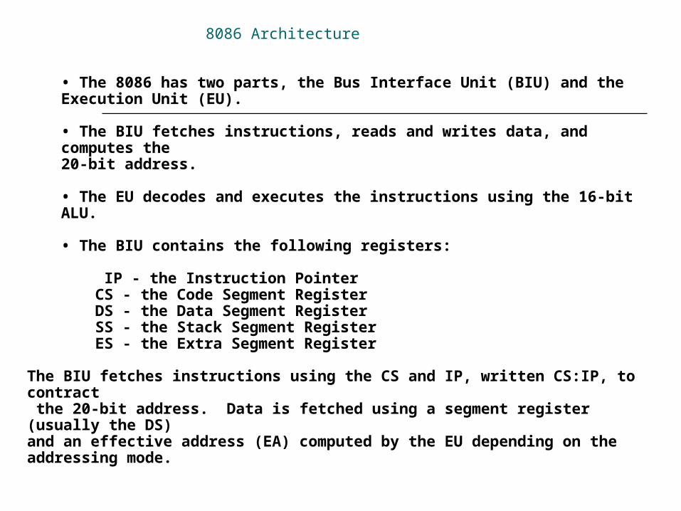
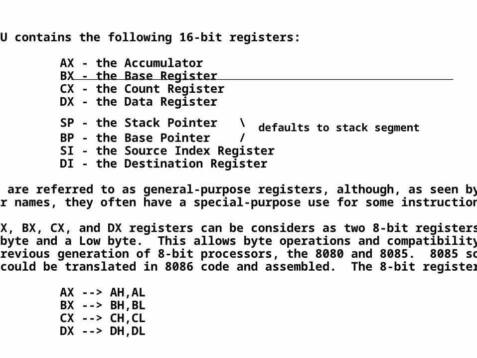
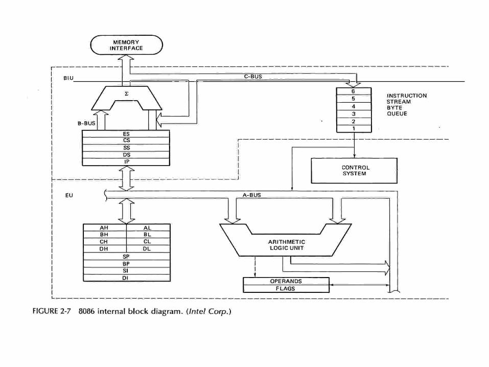
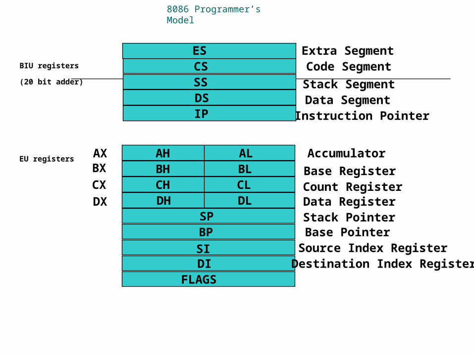
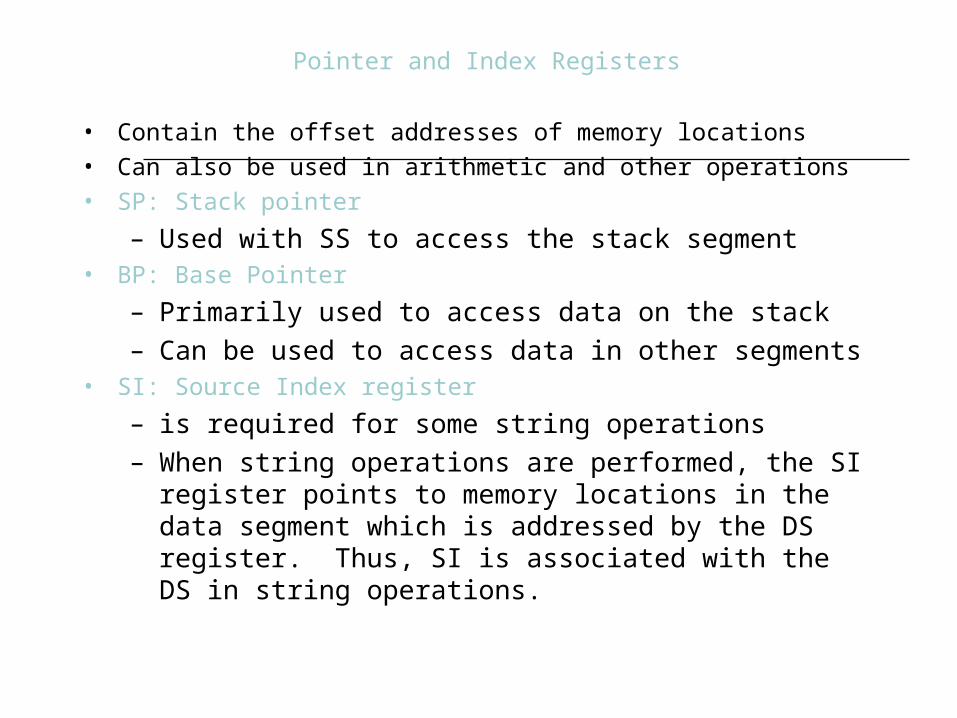
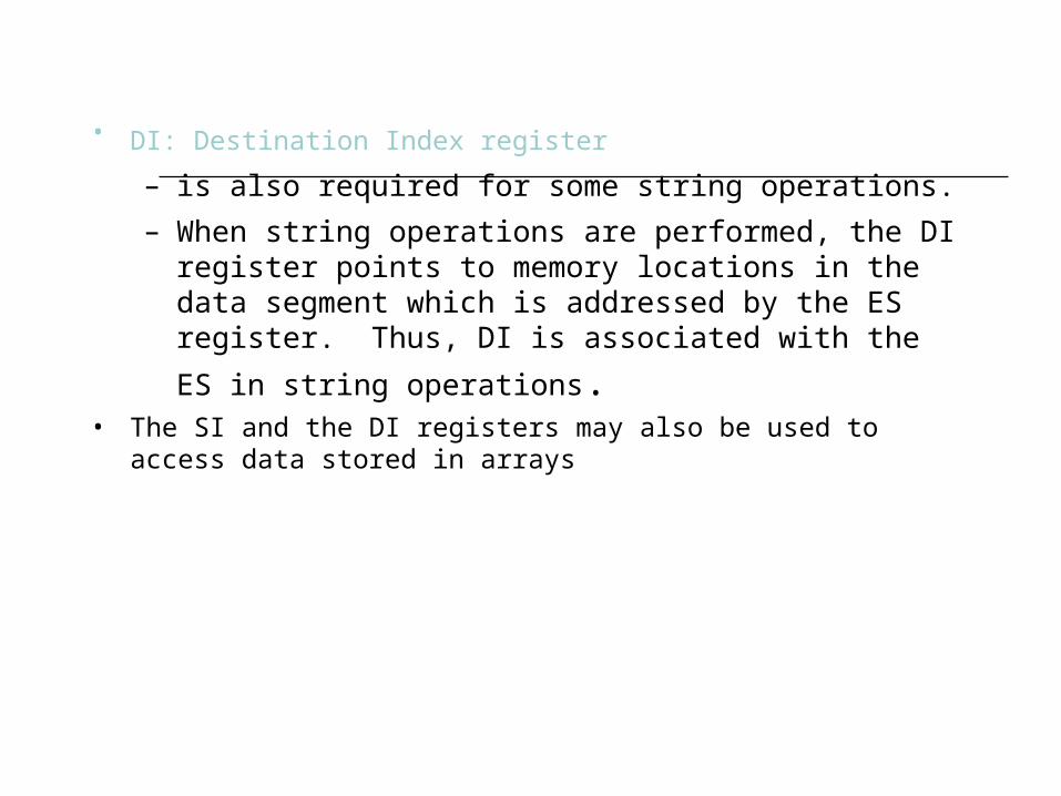
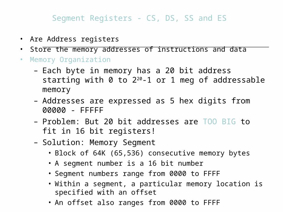
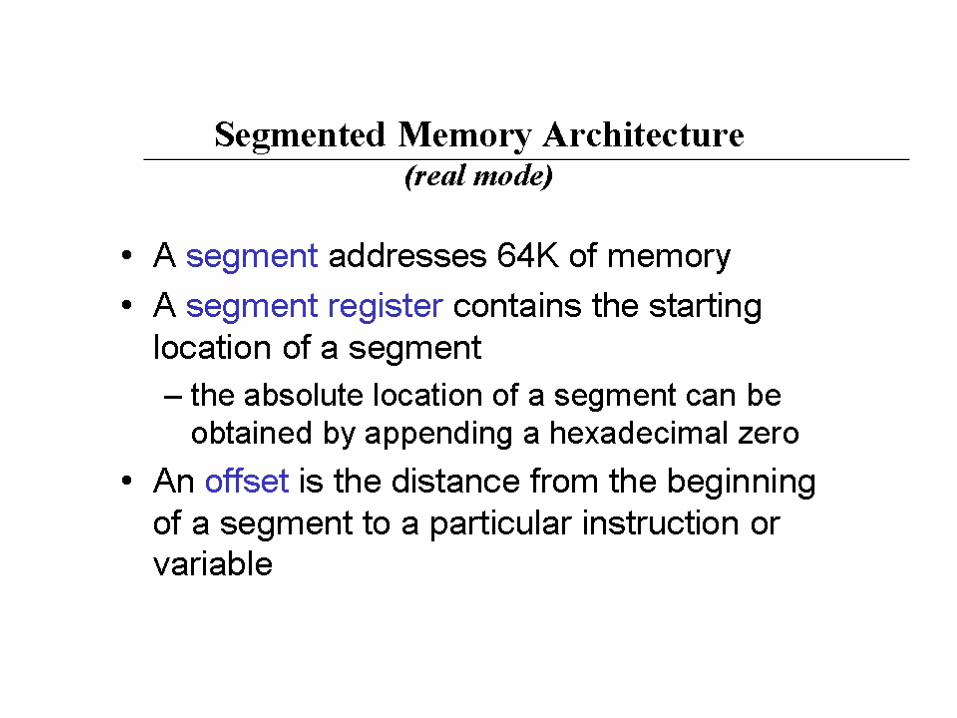
Memory Address Generation
Memory Address Generation
bull The BIU has a dedicated adder for determining physical memory addresses
Intel
Physical Address (20 Bits)
Adder
Segment Register (16 bits) 0 0 0 0
Offset Value (16 bits)
Example Address Calculation
Example Address Calculation
bull If the data segment starts at location 1000h and a data reference contains the address 29h where is the actual data
Intel
Offset 0 0 0 0 0 0 0 0 0 0 1 0 1 0 0 1
2 9
0 0 0 1 0 0 0 0 0 0 0 0 0 0 0 0 0 0 0 0Segment
0 0 0 1 0 0 0 0 0 0 0 0 0 0 1 0 1 0 0 1Address
SegmentOffset Address
bull Logical Address is specified as segmentoffsetbull Physical address is obtained by shifting the segment address 4
bits to the left and adding the offset addressbull Thus the physical address of the logical address A4FB4872 is
A4FB0+ 4872 A9822
Your turn
What linear address corresponds to the segmentoffset address 028F0030
028F0 + 0030 = 02920
Always use hexadecimal notation for addresses
Your turn
What segment addresses correspond to the linear address 28F30h
Many different segment-offset addresses can produce the linear address 28F30h For example
28F00030 28F30000 28B00430
The Code Segment
Memory
Segment Register
Offset
Physical orAbsolute Address
0
+
CS
IP
0400H
0056H
4000H
4056H
0400
0056
04056H
The offset is the distance in bytes from the start of the segmentThe offset is given by the IP for the Code SegmentInstructions are always fetched with using the CS register
CSIP = 40056Logical Address
0H
0FFFFFH
The physical address is also called the absolute address
The Data Segment
Memory
Segment Register
Offset
Physical Address
+
DS
EA
05C0
0050
05C00H
05C50H
05C0 0
0050
05C50H
Data is usually fetched with respect to the DS registerThe effective address (EA) is the offsetThe EA depends on the addressing mode
DSEA
0H
0FFFFFH
The Stack Segment
Memory
Segment Register
Offset
Physical Address
+
SS
SP
0A00
0100
0A000H
0A100H
0A00 0
0100
0A100H
The stack is always referenced with respect to the stack segment registerThe stack grows toward decreasing memory locationsThe SP points to the last or top item on the stack
PUSH - pre-decrement the SPPOP - post-increment the SP
The offset is given by the SP register
SSSP
0H
0FFFFFH
FlagsFlags
Carry flag
Parity flag
Auxiliary flag
Zero
Overflow
Direction
Interrupt enable
Trap
Sign6 are status flags3 are control flag
bull CF (carry) Contains carry from leftmost bit following arithmetic also contains last bit from a shift or rotate operation
Flag Register
Flag O D I T S Z A P C
Bit no 15 14 13 12 1110
9 8 7 6 5 4 3 2 1 0
bull Conditional flags ndash They are set according to some results of arithmetic
operation You do not need to alter the value yourselfbull Control flags
ndash Used to control some operations of the MPU These flags are to be set by you in order to achieve some specific
purposes
Flag Register
bull OF (overflow) Indicates overflow of the leftmost bit during arithmetic
bull DF (direction) Indicates left or right for moving or comparing string data
bull IF (interrupt) Indicates whether external interrupts are being processed or ignored
bull TF (trap) Permits operation of the processor in single step mode
bull SF (sign) Contains the resulting sign of an arithmetic operation (1=negative)
bull ZF (zero) Indicates when the result of arithmetic or a comparison is zero (1=yes)
bull AF (auxiliary carry) Contains carry out of bit 3 into bit 4 for specialized arithmetic
bull PF (parity) Indicates the number of 1 bits that result from an operation
Minimum-Mode and Maximum-Mode System
Minimum-Mode and Maximum-Mode System (cont)
Signals common to both minimum and maximum mode
Minimum-Mode and Maximum-Mode System (cont)
Unique minimum-mode signals
Minimum-Mode and Maximum-Mode System (cont)
Unique maximum-mode signals
Minimum-Mode and Maximum-Mode System (cont)
Minimum-Mode Interface
Block diagram of the minimum-mode 8088 MPU
Minimum-Mode Interface (cont)
Block diagram of the minimum-mode 8086 MPU
Minimum-Mode Interface (cont)
The minimum-mode signals can be divided into the following basic groups AddressData bus Status signals Control signals Interrupt signals DMA interface signals
Minimum-Mode Interface (cont)
AddressData bus The address bus is used to carry address information to
the memory and IO ports The address bus is 20-bit long and consists of signal lines
A0 through A19
A 20-bit address gives the 8088 a 1 Mbyte memory address space
Only address line A0 through A15 are used when addressing IO
This give an IO address space of 64 Kbytes The 8088 has 8 multiplexed addressdata bus lines
(A0~A7)
8086 has 16 multiplexed addressdata bus lines (A0~A15)
Minimum-Mode Interface (cont)
Status signals The four most significant address A19 through A16
are multiplexed with status signal S6 through S3
Bits S4 and S3 together form a 2-bit binary code that identifies which of the internal segment registers was used to generate the physical address
S5 is the logic level of the internal interrupt flag S6 is always at the 0 logic level
Minimum-Mode Interface (cont)
Minimum-Mode Interface (cont)
Minimum-Mode Interface (cont)
Maximum-Mode Interface
The maximum-mode configuration is mainly used for implementing a multiprocessorcoprocessor system environment Multiple processors exist in the system Each executes its own program
Global resources and local resources The former are common to all processors The latter are assigned to specific processors
In the maximum-mode facilities are provided for implementing allocation of global resources and passing bus control to other microprocessors sharing the system bus
Maximum-Mode Interface (cont)
8088 maximum-mode block diagram
Maximum-Mode Interface (cont)
8086 maximum-mode block diagram
Maximum-Mode Interface (cont)
8288 bus controller
Block diagram and pin layout of 8288
Maximum-Mode Interface (cont)
8288 bus controller In the maximum-mode 80888086 outputs a
status code on three signal line S0 S1 S2 prior to the initialization of each bus cycle
The 3-bit bus status code identifies which type of bus cycle is to follow and are input to the external bus controller device 8288
The 8288 produces one or two command signals for each bus cycle
Maximum-Mode Interface (cont)
8288 bus controller
Bus status code
Maximum-Mode Interface (cont)
Maximum-Mode Interface (cont)
Maximum-Mode Interface (cont)
Queue status signals The 2-bit queue status code QS0 and QS1 tells
the external circuitry what type of information was removed form the queue during the previous clock cycle
Queue status code
Electrical Characteristics
Power is applied between pin 40 (Vcc) and pins 1 (GND) and 20 (GND)
The nominal value of Vcc is specified as +5V dc with a tolerance of plusmn10
Both 8088 and 8086 draw a maximum of 340mA from the supply
IO voltage levels
System Clock
The time base for synchronization of the internal and external operations of the microprocessor in a microcomputer system is provided by the clock (CLK) input signal The standard 8088 operates at 5 MHz and the
8088-2 operates at 8 MHz The 8086 is manufactured in three speeds 5-
MHz 8086 8-MHz 8086-2 and the 10-MHz 8086-1
The CLK is externally generated by the 8284 clock generator and driver IC
System Clock (cont)
Block diagram of the 8284 clock generator
System Clock (cont)
Block diagram of the 8284 clock generator
System Clock (cont)
Connecting the 8284 to the 8088
15- or 24MHzcrystal
Typical value of CL when used with 15MHz crystal is 12pF
The fundamental crystal frequency is divided by 3 within the 8284 to give either a 5- or 8-MHz clock signal
System Clock (cont)
CLK waveform The signal is specified at Metal Oxide
Semiconductor (MOS)-compatible voltage level The period of the 5-MHz 8088 can range from
200 ns to 500 ns and the maximum rise and fall times of its edges equal 10 ns
System Clock (cont)
PCLK and OSC signals The peripheral clock (PCLK) and oscillator clock
(OSC) signals are provided to drive peripheral ICs The clock output at PCLK is half the frequency of
CLK The OSC output is at the crystal frequency which is three times of CLK
System Clock (cont)
The 8284 can also be driven from an external clock source Applied to the EFI (External Frequency Input) Input FC is used for selection
0 crystal between X1 and X2 is used 1 selects EFI
The CSYNC input is used for external synchronization in systems with multiple clocks
System Clock (cont)
EXAMPLE If the CLK input of an 8086 MPU is to be driven by
a 9-MHz signal what speed version of the 8086 must be used and what frequency crystal must be attached to the 8284
Solution The 8086-1 is the version of the 8086 that can be
run at 9-MHz To create the 9-MHz clock a 27-MHz crystal must be used on the 8284
Bus Cycle and Time States
A bus cycle defines the basic operation that a microprocessor performs to communicate with external devices
Examples of bus cycles are the memory read memory write inputoutput read and inputoutput write
The bus cycle of the 8088 and 8086 microprocessors consists of at least four clock periods
If no bus cycles are required the microprocessor performs what are known as idle states
When READY is held at the 0 level wait states are inserted between states T3 and T4 of the bus cycle
Bus Cycle and Time States (cont)
Bus cycle clock periods idle state and wait state
Bus Cycle and Time States (cont)
EXAMPLE What is the duration of the bus cycle in the 8088-
based microcomputer if the clock is 8 MHz and the two wait states are inserted
Solution The duration of the bus cycle in an 8 MHz system
is given by tcyc = 500 ns + N x 125 ns
In this expression the N stands for the number of waits states For a bus cycle with two wait states we get
tcyc = 500 ns + 2 x 125 ns = 500 ns + 250 ns = 750 ns
Hardware Organization of the Memory Address Space
1Mx8 memory bank of the 8088
Hardware Organization of the Memory Address Space (cont)
High and low memory banks of the 8086
Hardware Organization of the Memory Address Space (cont)
Byte transfer by the 8088
Hardware Organization of the Memory Address Space (cont)
Word transfer by the 8088
Hardware Organization of the Memory Address Space (cont)
Even address byte transfer by the 8086
Hardware Organization of the Memory Address Space (cont)
Odd address byte transfer by the 8086
Hardware Organization of the Memory Address Space (cont)
Even address word transfer by the 8086
Hardware Organization of the Memory Address Space (cont)
Odd-address word transfer by the 8086
Hardware Organization of the Memory Address Space (cont)
EXAMPLE Is the word at memory address 0123116 of an
8086-based microcomputer aligned or misaligned How many cycle are required to read it from memory
Solution The first byte of the word is the second byte at
the aligned-word address 0123016 Therefore the word is misaligned and required two bus cycles to be read from memory
Address Bus Status Codes
Whenever a memory bus cycle is in progress an address bus status code S4S3 is output by the processor S4S3 identifies which one of the four segment
register is used to generate the physical address in the current bus cycle 1048729
S4S3=00 identifies the extra segment register (ES)
S4S3=01 identifies the stack segment register (SS)
S4S3=10 identifies the code segment register (CS)
S4S3=11 identifies the data segment register (DS)
The memory address reach of the microprocessor can thus be expanded to 4 Mbytes
Memory Control Signals
Minimum-mode memory control signals
Memory Control Signals (cont)
Minimum-mode memory control signals (8088) ALE ndash Address Latch Enable ndash used to latch
the address in external memory IOM ndash Input-OutputMemory ndash signal external
circuitry whether a memory of IO bus cycle is in progress
DTR ndash Data TransmitReceive ndash signal external circuitry whether the 8088 is transmitting or receiving data over the bus 1048729
RD ndash Read ndash identifies that a read bus cycle is in progress
WR ndash Write ndash identifies that a write bus cycle is in progress
DEN ndash Data Enable ndash used to enable the data bus 1048729
SSO ndash Status Line ndash identifies whether a code or data access is in progress
Memory Control Signals (cont)
The control signals for the 8086rsquos minimum-mode memory interface differs in three ways IOM signal is replaced by MIO signal The signal SSO is removed from the interface BHE (bank high enable) is added to the interface
and is used to select input for the high bank of memory in the 8086rsquos memory subsystem
Memory Control Signals (cont)
Maximum-mode memory control signals
Memory Control Signals (cont)
Maximum-mode memory control signals MRDC ndash Memory Read Command 1048729 MWTC ndash Memory Write Command 1048729 AMWC ndash Advanced Memory Write Command
Read and Write Bus Cycle
Read cycle
Minimum-mode memory read bus cycle of the 8088
Read and Write Bus Cycle (cont)
Read cycle
Minimum-mode memory read bus cycle of the 8086
Read and Write Bus Cycle (cont)
Read cycle
Maximum-mode memory read bus cycle of the 8086
Read and Write Bus Cycle (cont)
Write cycle
Minimum-mode memory write bus cycle of the 8088
Read and Write Bus Cycle (cont)
Write cycle
Maximum-mode memory write bus cycle of the 8086
Memory Interface Circuit
Address bus latches and buffers Bank write and bank read control logic Data bus transceiversbuffers Address decoders
Memory Interface Circuit (cont)
Memory interface block diagram
Memory Interface Circuit (cont)
Address bus latches and buffers
Block diagram of a D-type latch
Memory Interface Circuit (cont)
Address bus latches and buffers
Circuit diagram of the 74F373
Memory Interface Circuit (cont)
A review of flip-floplatch logic
Positive edge-triggered D flip-flop
Memory Interface Circuit (cont)
A review of flip-floplatch logic
Positive edge-triggered JK flip-flop
Memory Interface Circuit (cont)
A review of flip-floplatch logic
D-type latch
Memory Interface Circuit (cont)
Address bus latches and buffers
Address latch circuit
Memory Interface Circuit (cont)
Bank write and bank read control logic
Bank write control logic Bank read control logic
Memory Interface Circuit (cont)
Data bus transceivers
Block diagram and circuit diagram of the 74F245 octal bus transceiver
Memory Interface Circuit (cont)
Data bus transceivers
Data bus transceiver circuit
Memory Interface Circuit (cont)
Address decoder
Address bus configuration with address decoding
Memory Interface Circuit (cont)
Address decoder
Block diagram and operation of the 74F139 decoder
Memory Interface Circuit (cont)
Address decoder
Circuit diagram of the 74F139 decoder
Memory Interface Circuit (cont)
Address decoder
Address decoder circuit using 74F139
Memory Interface Circuit (cont)
Address decoder
Block diagram and operation of the 74F138 decoder
Memory Interface Circuit (cont)
Address decoder
Circuit diagram of the 74F138 decoder
Memory Interface Circuit (cont)
Address decoder
Address decoder circuit using 74F138
Types of InputOutput
The IO system allows peripherals to provide data or receive results of processing the data Using IO ports
The 80888086 MPU can employ two types of IO Isolated IO Memory-mapped IO
They differ in how IO ports are mapped into the address space
Types of InputOutput (cont)
Isolated inputoutput When using isolated IO in a microcomputer
system the IO device are treated separate from memory
The memory address space contains 1 M consecutive byte address in the range 0000016 through FFFFF16
The IO address space contains 64K consecutive byte addresses in the range 000016 through FFFF16
The bytes in two consecutive IO addresses can be accessed as word-wide data
Page 0 000016 00FF16
Certain IO instructions can only perform in this range
Types of InputOutput (cont)
Isolated inputoutput
80888086 memory and IO address spaces
Types of InputOutput (cont)
Isolated inputoutput
Isolated IO ports
Types of InputOutput (cont)
Isolated inputoutput Advantages
The complete 1Mbyte memory address space is available for use with memory
Special instructions have been provided to perform IO operations with maximized performance
The bytes in two consecutive IO addresses can be accessed as word-wide data
Disadvantages All input and output data transfers must take place
between the AL or AX register and IO port
Types of InputOutput (cont)
Memory-mapped inputoutput MPU looks at the IO port as though it is a storage
location in memory Some of the memory address space is dedicated to IO
ports Instructions that affect data in memory are used
instead of the special IO instructions More instructions and addressing modes are available to
perform IO operations IO transfers can take place between IO port and other
internal registers The memory instructions tend to execute slower
than those specifically designed for isolated IO Part of the memory address space is lost
Types of InputOutput(cont)
Memory-mapped inputoutput
Memory mapped IO ports
Isolated InputOutput Interface
IO devices Keyboard Printer Mouse 82C55A etc
Functions of interface circuit Select the IO port Latch output data Sample input data Synchronize data transfer Translate between TTL voltage levels and those
required to operate the IO devices
Isolated InputOutput Interface (cont)
Minimum-mode interface
Minimum-mode 8088 system IO interface
Isolated InputOutput Interface (cont)
Minimum-mode interface
Minimum-mode 8086 system IO interface
Isolated InputOutput Interface (cont)
Maximum-mode interface
Maximum-mode 8088 system IO interface
Isolated InputOutput Interface (cont)
Maximum-mode interface
Maximum-mode 8086 system IO interface
Isolated InputOutput Interface (cont)
Maximum-mode interface
IO bus cycle status codes
InputOutput Data Transfer
Inputoutput data transfers in the 8088 and 8086 microcomputers can be either byte-wide or word-wide
IO addresses are 16 bits in length and are output by the 8088 to the IO interface over bus lines AD0 through AD7 and A8 through A15
In 8088 the word transfers is performed as two consecutive byte-wide data transfer and takes two bus cycle
In 8086 the word transfers can takes either one or two bus cycle
Word-wide IO ports should be aligned at even-address boundaries
InputOutput Data Instructions
InputOutput Data Instructions(cont)
EXAMPLE Write a sequence of instructions that will output
the data FF16 to a byte-wide output port at address AB16 of the IO address space
Solution First the AL register is loaded with FF16 as an
immediate operand in the instruction
MOV AL 0FFH Now the data in AL can be output to the byte-
wide output port with the instruction
OUT 0ABH AL
InputOutput Data Instructions(cont)
EXAMPLE Write a series of instructions that will output FF16 to an
output port located at address B00016 of the IO address space
Solution The DX register must first be loaded with the address
of the output port This is done with the instructionMOV DX 0B000H
Next the data that are to be output must be loaded into AL with the instruction
MOV AL 0FFH Finally the data are output with the instruction
OUT DX AL
InputOutput Data Instructions(cont)
EXAMPLE Data are to be read in from two byte-wide input
ports at addresses AA16 and A916 and then output as a word-wide output port at address B00016 Write a sequence of instructions to perform this inputoutput operation
InputOutput Data Instructions(cont)
Solution First read in the byte at address AA16 into AL and
move it into AHIN AL 0AAHMOV AH AL
Now the other byte can be read into AL by the instructionIN AL 09AH
And to write out the word of dataMOV DX 0B000HOUT DX AX
InputOutput Bus Cycles
Input bus cycle of the 8088
InputOutput Bus Cycles (cont)
Output bus cycle of the 8088
InputOutput Bus Cycles (cont)
Input bus cycle of the 8086
InputOutput Bus Cycles (cont)
Output bus cycle of the 8086
Example Address Calculation
Example Address Calculation
bull If the data segment starts at location 1000h and a data reference contains the address 29h where is the actual data
Intel
Offset 0 0 0 0 0 0 0 0 0 0 1 0 1 0 0 1
2 9
0 0 0 1 0 0 0 0 0 0 0 0 0 0 0 0 0 0 0 0Segment
0 0 0 1 0 0 0 0 0 0 0 0 0 0 1 0 1 0 0 1Address
SegmentOffset Address
bull Logical Address is specified as segmentoffsetbull Physical address is obtained by shifting the segment address 4
bits to the left and adding the offset addressbull Thus the physical address of the logical address A4FB4872 is
A4FB0+ 4872 A9822
Your turn
What linear address corresponds to the segmentoffset address 028F0030
028F0 + 0030 = 02920
Always use hexadecimal notation for addresses
Your turn
What segment addresses correspond to the linear address 28F30h
Many different segment-offset addresses can produce the linear address 28F30h For example
28F00030 28F30000 28B00430
The Code Segment
Memory
Segment Register
Offset
Physical orAbsolute Address
0
+
CS
IP
0400H
0056H
4000H
4056H
0400
0056
04056H
The offset is the distance in bytes from the start of the segmentThe offset is given by the IP for the Code SegmentInstructions are always fetched with using the CS register
CSIP = 40056Logical Address
0H
0FFFFFH
The physical address is also called the absolute address
The Data Segment
Memory
Segment Register
Offset
Physical Address
+
DS
EA
05C0
0050
05C00H
05C50H
05C0 0
0050
05C50H
Data is usually fetched with respect to the DS registerThe effective address (EA) is the offsetThe EA depends on the addressing mode
DSEA
0H
0FFFFFH
The Stack Segment
Memory
Segment Register
Offset
Physical Address
+
SS
SP
0A00
0100
0A000H
0A100H
0A00 0
0100
0A100H
The stack is always referenced with respect to the stack segment registerThe stack grows toward decreasing memory locationsThe SP points to the last or top item on the stack
PUSH - pre-decrement the SPPOP - post-increment the SP
The offset is given by the SP register
SSSP
0H
0FFFFFH
FlagsFlags
Carry flag
Parity flag
Auxiliary flag
Zero
Overflow
Direction
Interrupt enable
Trap
Sign6 are status flags3 are control flag
bull CF (carry) Contains carry from leftmost bit following arithmetic also contains last bit from a shift or rotate operation
Flag Register
Flag O D I T S Z A P C
Bit no 15 14 13 12 1110
9 8 7 6 5 4 3 2 1 0
bull Conditional flags ndash They are set according to some results of arithmetic
operation You do not need to alter the value yourselfbull Control flags
ndash Used to control some operations of the MPU These flags are to be set by you in order to achieve some specific
purposes
Flag Register
bull OF (overflow) Indicates overflow of the leftmost bit during arithmetic
bull DF (direction) Indicates left or right for moving or comparing string data
bull IF (interrupt) Indicates whether external interrupts are being processed or ignored
bull TF (trap) Permits operation of the processor in single step mode
bull SF (sign) Contains the resulting sign of an arithmetic operation (1=negative)
bull ZF (zero) Indicates when the result of arithmetic or a comparison is zero (1=yes)
bull AF (auxiliary carry) Contains carry out of bit 3 into bit 4 for specialized arithmetic
bull PF (parity) Indicates the number of 1 bits that result from an operation
Minimum-Mode and Maximum-Mode System
Minimum-Mode and Maximum-Mode System (cont)
Signals common to both minimum and maximum mode
Minimum-Mode and Maximum-Mode System (cont)
Unique minimum-mode signals
Minimum-Mode and Maximum-Mode System (cont)
Unique maximum-mode signals
Minimum-Mode and Maximum-Mode System (cont)
Minimum-Mode Interface
Block diagram of the minimum-mode 8088 MPU
Minimum-Mode Interface (cont)
Block diagram of the minimum-mode 8086 MPU
Minimum-Mode Interface (cont)
The minimum-mode signals can be divided into the following basic groups AddressData bus Status signals Control signals Interrupt signals DMA interface signals
Minimum-Mode Interface (cont)
AddressData bus The address bus is used to carry address information to
the memory and IO ports The address bus is 20-bit long and consists of signal lines
A0 through A19
A 20-bit address gives the 8088 a 1 Mbyte memory address space
Only address line A0 through A15 are used when addressing IO
This give an IO address space of 64 Kbytes The 8088 has 8 multiplexed addressdata bus lines
(A0~A7)
8086 has 16 multiplexed addressdata bus lines (A0~A15)
Minimum-Mode Interface (cont)
Status signals The four most significant address A19 through A16
are multiplexed with status signal S6 through S3
Bits S4 and S3 together form a 2-bit binary code that identifies which of the internal segment registers was used to generate the physical address
S5 is the logic level of the internal interrupt flag S6 is always at the 0 logic level
Minimum-Mode Interface (cont)
Minimum-Mode Interface (cont)
Minimum-Mode Interface (cont)
Maximum-Mode Interface
The maximum-mode configuration is mainly used for implementing a multiprocessorcoprocessor system environment Multiple processors exist in the system Each executes its own program
Global resources and local resources The former are common to all processors The latter are assigned to specific processors
In the maximum-mode facilities are provided for implementing allocation of global resources and passing bus control to other microprocessors sharing the system bus
Maximum-Mode Interface (cont)
8088 maximum-mode block diagram
Maximum-Mode Interface (cont)
8086 maximum-mode block diagram
Maximum-Mode Interface (cont)
8288 bus controller
Block diagram and pin layout of 8288
Maximum-Mode Interface (cont)
8288 bus controller In the maximum-mode 80888086 outputs a
status code on three signal line S0 S1 S2 prior to the initialization of each bus cycle
The 3-bit bus status code identifies which type of bus cycle is to follow and are input to the external bus controller device 8288
The 8288 produces one or two command signals for each bus cycle
Maximum-Mode Interface (cont)
8288 bus controller
Bus status code
Maximum-Mode Interface (cont)
Maximum-Mode Interface (cont)
Maximum-Mode Interface (cont)
Queue status signals The 2-bit queue status code QS0 and QS1 tells
the external circuitry what type of information was removed form the queue during the previous clock cycle
Queue status code
Electrical Characteristics
Power is applied between pin 40 (Vcc) and pins 1 (GND) and 20 (GND)
The nominal value of Vcc is specified as +5V dc with a tolerance of plusmn10
Both 8088 and 8086 draw a maximum of 340mA from the supply
IO voltage levels
System Clock
The time base for synchronization of the internal and external operations of the microprocessor in a microcomputer system is provided by the clock (CLK) input signal The standard 8088 operates at 5 MHz and the
8088-2 operates at 8 MHz The 8086 is manufactured in three speeds 5-
MHz 8086 8-MHz 8086-2 and the 10-MHz 8086-1
The CLK is externally generated by the 8284 clock generator and driver IC
System Clock (cont)
Block diagram of the 8284 clock generator
System Clock (cont)
Block diagram of the 8284 clock generator
System Clock (cont)
Connecting the 8284 to the 8088
15- or 24MHzcrystal
Typical value of CL when used with 15MHz crystal is 12pF
The fundamental crystal frequency is divided by 3 within the 8284 to give either a 5- or 8-MHz clock signal
System Clock (cont)
CLK waveform The signal is specified at Metal Oxide
Semiconductor (MOS)-compatible voltage level The period of the 5-MHz 8088 can range from
200 ns to 500 ns and the maximum rise and fall times of its edges equal 10 ns
System Clock (cont)
PCLK and OSC signals The peripheral clock (PCLK) and oscillator clock
(OSC) signals are provided to drive peripheral ICs The clock output at PCLK is half the frequency of
CLK The OSC output is at the crystal frequency which is three times of CLK
System Clock (cont)
The 8284 can also be driven from an external clock source Applied to the EFI (External Frequency Input) Input FC is used for selection
0 crystal between X1 and X2 is used 1 selects EFI
The CSYNC input is used for external synchronization in systems with multiple clocks
System Clock (cont)
EXAMPLE If the CLK input of an 8086 MPU is to be driven by
a 9-MHz signal what speed version of the 8086 must be used and what frequency crystal must be attached to the 8284
Solution The 8086-1 is the version of the 8086 that can be
run at 9-MHz To create the 9-MHz clock a 27-MHz crystal must be used on the 8284
Bus Cycle and Time States
A bus cycle defines the basic operation that a microprocessor performs to communicate with external devices
Examples of bus cycles are the memory read memory write inputoutput read and inputoutput write
The bus cycle of the 8088 and 8086 microprocessors consists of at least four clock periods
If no bus cycles are required the microprocessor performs what are known as idle states
When READY is held at the 0 level wait states are inserted between states T3 and T4 of the bus cycle
Bus Cycle and Time States (cont)
Bus cycle clock periods idle state and wait state
Bus Cycle and Time States (cont)
EXAMPLE What is the duration of the bus cycle in the 8088-
based microcomputer if the clock is 8 MHz and the two wait states are inserted
Solution The duration of the bus cycle in an 8 MHz system
is given by tcyc = 500 ns + N x 125 ns
In this expression the N stands for the number of waits states For a bus cycle with two wait states we get
tcyc = 500 ns + 2 x 125 ns = 500 ns + 250 ns = 750 ns
Hardware Organization of the Memory Address Space
1Mx8 memory bank of the 8088
Hardware Organization of the Memory Address Space (cont)
High and low memory banks of the 8086
Hardware Organization of the Memory Address Space (cont)
Byte transfer by the 8088
Hardware Organization of the Memory Address Space (cont)
Word transfer by the 8088
Hardware Organization of the Memory Address Space (cont)
Even address byte transfer by the 8086
Hardware Organization of the Memory Address Space (cont)
Odd address byte transfer by the 8086
Hardware Organization of the Memory Address Space (cont)
Even address word transfer by the 8086
Hardware Organization of the Memory Address Space (cont)
Odd-address word transfer by the 8086
Hardware Organization of the Memory Address Space (cont)
EXAMPLE Is the word at memory address 0123116 of an
8086-based microcomputer aligned or misaligned How many cycle are required to read it from memory
Solution The first byte of the word is the second byte at
the aligned-word address 0123016 Therefore the word is misaligned and required two bus cycles to be read from memory
Address Bus Status Codes
Whenever a memory bus cycle is in progress an address bus status code S4S3 is output by the processor S4S3 identifies which one of the four segment
register is used to generate the physical address in the current bus cycle 1048729
S4S3=00 identifies the extra segment register (ES)
S4S3=01 identifies the stack segment register (SS)
S4S3=10 identifies the code segment register (CS)
S4S3=11 identifies the data segment register (DS)
The memory address reach of the microprocessor can thus be expanded to 4 Mbytes
Memory Control Signals
Minimum-mode memory control signals
Memory Control Signals (cont)
Minimum-mode memory control signals (8088) ALE ndash Address Latch Enable ndash used to latch
the address in external memory IOM ndash Input-OutputMemory ndash signal external
circuitry whether a memory of IO bus cycle is in progress
DTR ndash Data TransmitReceive ndash signal external circuitry whether the 8088 is transmitting or receiving data over the bus 1048729
RD ndash Read ndash identifies that a read bus cycle is in progress
WR ndash Write ndash identifies that a write bus cycle is in progress
DEN ndash Data Enable ndash used to enable the data bus 1048729
SSO ndash Status Line ndash identifies whether a code or data access is in progress
Memory Control Signals (cont)
The control signals for the 8086rsquos minimum-mode memory interface differs in three ways IOM signal is replaced by MIO signal The signal SSO is removed from the interface BHE (bank high enable) is added to the interface
and is used to select input for the high bank of memory in the 8086rsquos memory subsystem
Memory Control Signals (cont)
Maximum-mode memory control signals
Memory Control Signals (cont)
Maximum-mode memory control signals MRDC ndash Memory Read Command 1048729 MWTC ndash Memory Write Command 1048729 AMWC ndash Advanced Memory Write Command
Read and Write Bus Cycle
Read cycle
Minimum-mode memory read bus cycle of the 8088
Read and Write Bus Cycle (cont)
Read cycle
Minimum-mode memory read bus cycle of the 8086
Read and Write Bus Cycle (cont)
Read cycle
Maximum-mode memory read bus cycle of the 8086
Read and Write Bus Cycle (cont)
Write cycle
Minimum-mode memory write bus cycle of the 8088
Read and Write Bus Cycle (cont)
Write cycle
Maximum-mode memory write bus cycle of the 8086
Memory Interface Circuit
Address bus latches and buffers Bank write and bank read control logic Data bus transceiversbuffers Address decoders
Memory Interface Circuit (cont)
Memory interface block diagram
Memory Interface Circuit (cont)
Address bus latches and buffers
Block diagram of a D-type latch
Memory Interface Circuit (cont)
Address bus latches and buffers
Circuit diagram of the 74F373
Memory Interface Circuit (cont)
A review of flip-floplatch logic
Positive edge-triggered D flip-flop
Memory Interface Circuit (cont)
A review of flip-floplatch logic
Positive edge-triggered JK flip-flop
Memory Interface Circuit (cont)
A review of flip-floplatch logic
D-type latch
Memory Interface Circuit (cont)
Address bus latches and buffers
Address latch circuit
Memory Interface Circuit (cont)
Bank write and bank read control logic
Bank write control logic Bank read control logic
Memory Interface Circuit (cont)
Data bus transceivers
Block diagram and circuit diagram of the 74F245 octal bus transceiver
Memory Interface Circuit (cont)
Data bus transceivers
Data bus transceiver circuit
Memory Interface Circuit (cont)
Address decoder
Address bus configuration with address decoding
Memory Interface Circuit (cont)
Address decoder
Block diagram and operation of the 74F139 decoder
Memory Interface Circuit (cont)
Address decoder
Circuit diagram of the 74F139 decoder
Memory Interface Circuit (cont)
Address decoder
Address decoder circuit using 74F139
Memory Interface Circuit (cont)
Address decoder
Block diagram and operation of the 74F138 decoder
Memory Interface Circuit (cont)
Address decoder
Circuit diagram of the 74F138 decoder
Memory Interface Circuit (cont)
Address decoder
Address decoder circuit using 74F138
Types of InputOutput
The IO system allows peripherals to provide data or receive results of processing the data Using IO ports
The 80888086 MPU can employ two types of IO Isolated IO Memory-mapped IO
They differ in how IO ports are mapped into the address space
Types of InputOutput (cont)
Isolated inputoutput When using isolated IO in a microcomputer
system the IO device are treated separate from memory
The memory address space contains 1 M consecutive byte address in the range 0000016 through FFFFF16
The IO address space contains 64K consecutive byte addresses in the range 000016 through FFFF16
The bytes in two consecutive IO addresses can be accessed as word-wide data
Page 0 000016 00FF16
Certain IO instructions can only perform in this range
Types of InputOutput (cont)
Isolated inputoutput
80888086 memory and IO address spaces
Types of InputOutput (cont)
Isolated inputoutput
Isolated IO ports
Types of InputOutput (cont)
Isolated inputoutput Advantages
The complete 1Mbyte memory address space is available for use with memory
Special instructions have been provided to perform IO operations with maximized performance
The bytes in two consecutive IO addresses can be accessed as word-wide data
Disadvantages All input and output data transfers must take place
between the AL or AX register and IO port
Types of InputOutput (cont)
Memory-mapped inputoutput MPU looks at the IO port as though it is a storage
location in memory Some of the memory address space is dedicated to IO
ports Instructions that affect data in memory are used
instead of the special IO instructions More instructions and addressing modes are available to
perform IO operations IO transfers can take place between IO port and other
internal registers The memory instructions tend to execute slower
than those specifically designed for isolated IO Part of the memory address space is lost
Types of InputOutput(cont)
Memory-mapped inputoutput
Memory mapped IO ports
Isolated InputOutput Interface
IO devices Keyboard Printer Mouse 82C55A etc
Functions of interface circuit Select the IO port Latch output data Sample input data Synchronize data transfer Translate between TTL voltage levels and those
required to operate the IO devices
Isolated InputOutput Interface (cont)
Minimum-mode interface
Minimum-mode 8088 system IO interface
Isolated InputOutput Interface (cont)
Minimum-mode interface
Minimum-mode 8086 system IO interface
Isolated InputOutput Interface (cont)
Maximum-mode interface
Maximum-mode 8088 system IO interface
Isolated InputOutput Interface (cont)
Maximum-mode interface
Maximum-mode 8086 system IO interface
Isolated InputOutput Interface (cont)
Maximum-mode interface
IO bus cycle status codes
InputOutput Data Transfer
Inputoutput data transfers in the 8088 and 8086 microcomputers can be either byte-wide or word-wide
IO addresses are 16 bits in length and are output by the 8088 to the IO interface over bus lines AD0 through AD7 and A8 through A15
In 8088 the word transfers is performed as two consecutive byte-wide data transfer and takes two bus cycle
In 8086 the word transfers can takes either one or two bus cycle
Word-wide IO ports should be aligned at even-address boundaries
InputOutput Data Instructions
InputOutput Data Instructions(cont)
EXAMPLE Write a sequence of instructions that will output
the data FF16 to a byte-wide output port at address AB16 of the IO address space
Solution First the AL register is loaded with FF16 as an
immediate operand in the instruction
MOV AL 0FFH Now the data in AL can be output to the byte-
wide output port with the instruction
OUT 0ABH AL
InputOutput Data Instructions(cont)
EXAMPLE Write a series of instructions that will output FF16 to an
output port located at address B00016 of the IO address space
Solution The DX register must first be loaded with the address
of the output port This is done with the instructionMOV DX 0B000H
Next the data that are to be output must be loaded into AL with the instruction
MOV AL 0FFH Finally the data are output with the instruction
OUT DX AL
InputOutput Data Instructions(cont)
EXAMPLE Data are to be read in from two byte-wide input
ports at addresses AA16 and A916 and then output as a word-wide output port at address B00016 Write a sequence of instructions to perform this inputoutput operation
InputOutput Data Instructions(cont)
Solution First read in the byte at address AA16 into AL and
move it into AHIN AL 0AAHMOV AH AL
Now the other byte can be read into AL by the instructionIN AL 09AH
And to write out the word of dataMOV DX 0B000HOUT DX AX
InputOutput Bus Cycles
Input bus cycle of the 8088
InputOutput Bus Cycles (cont)
Output bus cycle of the 8088
InputOutput Bus Cycles (cont)
Input bus cycle of the 8086
InputOutput Bus Cycles (cont)
Output bus cycle of the 8086
Your turn
What segment addresses correspond to the linear address 28F30h
Many different segment-offset addresses can produce the linear address 28F30h For example
28F00030 28F30000 28B00430
The Code Segment
Memory
Segment Register
Offset
Physical orAbsolute Address
0
+
CS
IP
0400H
0056H
4000H
4056H
0400
0056
04056H
The offset is the distance in bytes from the start of the segmentThe offset is given by the IP for the Code SegmentInstructions are always fetched with using the CS register
CSIP = 40056Logical Address
0H
0FFFFFH
The physical address is also called the absolute address
The Data Segment
Memory
Segment Register
Offset
Physical Address
+
DS
EA
05C0
0050
05C00H
05C50H
05C0 0
0050
05C50H
Data is usually fetched with respect to the DS registerThe effective address (EA) is the offsetThe EA depends on the addressing mode
DSEA
0H
0FFFFFH
The Stack Segment
Memory
Segment Register
Offset
Physical Address
+
SS
SP
0A00
0100
0A000H
0A100H
0A00 0
0100
0A100H
The stack is always referenced with respect to the stack segment registerThe stack grows toward decreasing memory locationsThe SP points to the last or top item on the stack
PUSH - pre-decrement the SPPOP - post-increment the SP
The offset is given by the SP register
SSSP
0H
0FFFFFH
FlagsFlags
Carry flag
Parity flag
Auxiliary flag
Zero
Overflow
Direction
Interrupt enable
Trap
Sign6 are status flags3 are control flag
bull CF (carry) Contains carry from leftmost bit following arithmetic also contains last bit from a shift or rotate operation
Flag Register
Flag O D I T S Z A P C
Bit no 15 14 13 12 1110
9 8 7 6 5 4 3 2 1 0
bull Conditional flags ndash They are set according to some results of arithmetic
operation You do not need to alter the value yourselfbull Control flags
ndash Used to control some operations of the MPU These flags are to be set by you in order to achieve some specific
purposes
Flag Register
bull OF (overflow) Indicates overflow of the leftmost bit during arithmetic
bull DF (direction) Indicates left or right for moving or comparing string data
bull IF (interrupt) Indicates whether external interrupts are being processed or ignored
bull TF (trap) Permits operation of the processor in single step mode
bull SF (sign) Contains the resulting sign of an arithmetic operation (1=negative)
bull ZF (zero) Indicates when the result of arithmetic or a comparison is zero (1=yes)
bull AF (auxiliary carry) Contains carry out of bit 3 into bit 4 for specialized arithmetic
bull PF (parity) Indicates the number of 1 bits that result from an operation
Minimum-Mode and Maximum-Mode System
Minimum-Mode and Maximum-Mode System (cont)
Signals common to both minimum and maximum mode
Minimum-Mode and Maximum-Mode System (cont)
Unique minimum-mode signals
Minimum-Mode and Maximum-Mode System (cont)
Unique maximum-mode signals
Minimum-Mode and Maximum-Mode System (cont)
Minimum-Mode Interface
Block diagram of the minimum-mode 8088 MPU
Minimum-Mode Interface (cont)
Block diagram of the minimum-mode 8086 MPU
Minimum-Mode Interface (cont)
The minimum-mode signals can be divided into the following basic groups AddressData bus Status signals Control signals Interrupt signals DMA interface signals
Minimum-Mode Interface (cont)
AddressData bus The address bus is used to carry address information to
the memory and IO ports The address bus is 20-bit long and consists of signal lines
A0 through A19
A 20-bit address gives the 8088 a 1 Mbyte memory address space
Only address line A0 through A15 are used when addressing IO
This give an IO address space of 64 Kbytes The 8088 has 8 multiplexed addressdata bus lines
(A0~A7)
8086 has 16 multiplexed addressdata bus lines (A0~A15)
Minimum-Mode Interface (cont)
Status signals The four most significant address A19 through A16
are multiplexed with status signal S6 through S3
Bits S4 and S3 together form a 2-bit binary code that identifies which of the internal segment registers was used to generate the physical address
S5 is the logic level of the internal interrupt flag S6 is always at the 0 logic level
Minimum-Mode Interface (cont)
Minimum-Mode Interface (cont)
Minimum-Mode Interface (cont)
Maximum-Mode Interface
The maximum-mode configuration is mainly used for implementing a multiprocessorcoprocessor system environment Multiple processors exist in the system Each executes its own program
Global resources and local resources The former are common to all processors The latter are assigned to specific processors
In the maximum-mode facilities are provided for implementing allocation of global resources and passing bus control to other microprocessors sharing the system bus
Maximum-Mode Interface (cont)
8088 maximum-mode block diagram
Maximum-Mode Interface (cont)
8086 maximum-mode block diagram
Maximum-Mode Interface (cont)
8288 bus controller
Block diagram and pin layout of 8288
Maximum-Mode Interface (cont)
8288 bus controller In the maximum-mode 80888086 outputs a
status code on three signal line S0 S1 S2 prior to the initialization of each bus cycle
The 3-bit bus status code identifies which type of bus cycle is to follow and are input to the external bus controller device 8288
The 8288 produces one or two command signals for each bus cycle
Maximum-Mode Interface (cont)
8288 bus controller
Bus status code
Maximum-Mode Interface (cont)
Maximum-Mode Interface (cont)
Maximum-Mode Interface (cont)
Queue status signals The 2-bit queue status code QS0 and QS1 tells
the external circuitry what type of information was removed form the queue during the previous clock cycle
Queue status code
Electrical Characteristics
Power is applied between pin 40 (Vcc) and pins 1 (GND) and 20 (GND)
The nominal value of Vcc is specified as +5V dc with a tolerance of plusmn10
Both 8088 and 8086 draw a maximum of 340mA from the supply
IO voltage levels
System Clock
The time base for synchronization of the internal and external operations of the microprocessor in a microcomputer system is provided by the clock (CLK) input signal The standard 8088 operates at 5 MHz and the
8088-2 operates at 8 MHz The 8086 is manufactured in three speeds 5-
MHz 8086 8-MHz 8086-2 and the 10-MHz 8086-1
The CLK is externally generated by the 8284 clock generator and driver IC
System Clock (cont)
Block diagram of the 8284 clock generator
System Clock (cont)
Block diagram of the 8284 clock generator
System Clock (cont)
Connecting the 8284 to the 8088
15- or 24MHzcrystal
Typical value of CL when used with 15MHz crystal is 12pF
The fundamental crystal frequency is divided by 3 within the 8284 to give either a 5- or 8-MHz clock signal
System Clock (cont)
CLK waveform The signal is specified at Metal Oxide
Semiconductor (MOS)-compatible voltage level The period of the 5-MHz 8088 can range from
200 ns to 500 ns and the maximum rise and fall times of its edges equal 10 ns
System Clock (cont)
PCLK and OSC signals The peripheral clock (PCLK) and oscillator clock
(OSC) signals are provided to drive peripheral ICs The clock output at PCLK is half the frequency of
CLK The OSC output is at the crystal frequency which is three times of CLK
System Clock (cont)
The 8284 can also be driven from an external clock source Applied to the EFI (External Frequency Input) Input FC is used for selection
0 crystal between X1 and X2 is used 1 selects EFI
The CSYNC input is used for external synchronization in systems with multiple clocks
System Clock (cont)
EXAMPLE If the CLK input of an 8086 MPU is to be driven by
a 9-MHz signal what speed version of the 8086 must be used and what frequency crystal must be attached to the 8284
Solution The 8086-1 is the version of the 8086 that can be
run at 9-MHz To create the 9-MHz clock a 27-MHz crystal must be used on the 8284
Bus Cycle and Time States
A bus cycle defines the basic operation that a microprocessor performs to communicate with external devices
Examples of bus cycles are the memory read memory write inputoutput read and inputoutput write
The bus cycle of the 8088 and 8086 microprocessors consists of at least four clock periods
If no bus cycles are required the microprocessor performs what are known as idle states
When READY is held at the 0 level wait states are inserted between states T3 and T4 of the bus cycle
Bus Cycle and Time States (cont)
Bus cycle clock periods idle state and wait state
Bus Cycle and Time States (cont)
EXAMPLE What is the duration of the bus cycle in the 8088-
based microcomputer if the clock is 8 MHz and the two wait states are inserted
Solution The duration of the bus cycle in an 8 MHz system
is given by tcyc = 500 ns + N x 125 ns
In this expression the N stands for the number of waits states For a bus cycle with two wait states we get
tcyc = 500 ns + 2 x 125 ns = 500 ns + 250 ns = 750 ns
Hardware Organization of the Memory Address Space
1Mx8 memory bank of the 8088
Hardware Organization of the Memory Address Space (cont)
High and low memory banks of the 8086
Hardware Organization of the Memory Address Space (cont)
Byte transfer by the 8088
Hardware Organization of the Memory Address Space (cont)
Word transfer by the 8088
Hardware Organization of the Memory Address Space (cont)
Even address byte transfer by the 8086
Hardware Organization of the Memory Address Space (cont)
Odd address byte transfer by the 8086
Hardware Organization of the Memory Address Space (cont)
Even address word transfer by the 8086
Hardware Organization of the Memory Address Space (cont)
Odd-address word transfer by the 8086
Hardware Organization of the Memory Address Space (cont)
EXAMPLE Is the word at memory address 0123116 of an
8086-based microcomputer aligned or misaligned How many cycle are required to read it from memory
Solution The first byte of the word is the second byte at
the aligned-word address 0123016 Therefore the word is misaligned and required two bus cycles to be read from memory
Address Bus Status Codes
Whenever a memory bus cycle is in progress an address bus status code S4S3 is output by the processor S4S3 identifies which one of the four segment
register is used to generate the physical address in the current bus cycle 1048729
S4S3=00 identifies the extra segment register (ES)
S4S3=01 identifies the stack segment register (SS)
S4S3=10 identifies the code segment register (CS)
S4S3=11 identifies the data segment register (DS)
The memory address reach of the microprocessor can thus be expanded to 4 Mbytes
Memory Control Signals
Minimum-mode memory control signals
Memory Control Signals (cont)
Minimum-mode memory control signals (8088) ALE ndash Address Latch Enable ndash used to latch
the address in external memory IOM ndash Input-OutputMemory ndash signal external
circuitry whether a memory of IO bus cycle is in progress
DTR ndash Data TransmitReceive ndash signal external circuitry whether the 8088 is transmitting or receiving data over the bus 1048729
RD ndash Read ndash identifies that a read bus cycle is in progress
WR ndash Write ndash identifies that a write bus cycle is in progress
DEN ndash Data Enable ndash used to enable the data bus 1048729
SSO ndash Status Line ndash identifies whether a code or data access is in progress
Memory Control Signals (cont)
The control signals for the 8086rsquos minimum-mode memory interface differs in three ways IOM signal is replaced by MIO signal The signal SSO is removed from the interface BHE (bank high enable) is added to the interface
and is used to select input for the high bank of memory in the 8086rsquos memory subsystem
Memory Control Signals (cont)
Maximum-mode memory control signals
Memory Control Signals (cont)
Maximum-mode memory control signals MRDC ndash Memory Read Command 1048729 MWTC ndash Memory Write Command 1048729 AMWC ndash Advanced Memory Write Command
Read and Write Bus Cycle
Read cycle
Minimum-mode memory read bus cycle of the 8088
Read and Write Bus Cycle (cont)
Read cycle
Minimum-mode memory read bus cycle of the 8086
Read and Write Bus Cycle (cont)
Read cycle
Maximum-mode memory read bus cycle of the 8086
Read and Write Bus Cycle (cont)
Write cycle
Minimum-mode memory write bus cycle of the 8088
Read and Write Bus Cycle (cont)
Write cycle
Maximum-mode memory write bus cycle of the 8086
Memory Interface Circuit
Address bus latches and buffers Bank write and bank read control logic Data bus transceiversbuffers Address decoders
Memory Interface Circuit (cont)
Memory interface block diagram
Memory Interface Circuit (cont)
Address bus latches and buffers
Block diagram of a D-type latch
Memory Interface Circuit (cont)
Address bus latches and buffers
Circuit diagram of the 74F373
Memory Interface Circuit (cont)
A review of flip-floplatch logic
Positive edge-triggered D flip-flop
Memory Interface Circuit (cont)
A review of flip-floplatch logic
Positive edge-triggered JK flip-flop
Memory Interface Circuit (cont)
A review of flip-floplatch logic
D-type latch
Memory Interface Circuit (cont)
Address bus latches and buffers
Address latch circuit
Memory Interface Circuit (cont)
Bank write and bank read control logic
Bank write control logic Bank read control logic
Memory Interface Circuit (cont)
Data bus transceivers
Block diagram and circuit diagram of the 74F245 octal bus transceiver
Memory Interface Circuit (cont)
Data bus transceivers
Data bus transceiver circuit
Memory Interface Circuit (cont)
Address decoder
Address bus configuration with address decoding
Memory Interface Circuit (cont)
Address decoder
Block diagram and operation of the 74F139 decoder
Memory Interface Circuit (cont)
Address decoder
Circuit diagram of the 74F139 decoder
Memory Interface Circuit (cont)
Address decoder
Address decoder circuit using 74F139
Memory Interface Circuit (cont)
Address decoder
Block diagram and operation of the 74F138 decoder
Memory Interface Circuit (cont)
Address decoder
Circuit diagram of the 74F138 decoder
Memory Interface Circuit (cont)
Address decoder
Address decoder circuit using 74F138
Types of InputOutput
The IO system allows peripherals to provide data or receive results of processing the data Using IO ports
The 80888086 MPU can employ two types of IO Isolated IO Memory-mapped IO
They differ in how IO ports are mapped into the address space
Types of InputOutput (cont)
Isolated inputoutput When using isolated IO in a microcomputer
system the IO device are treated separate from memory
The memory address space contains 1 M consecutive byte address in the range 0000016 through FFFFF16
The IO address space contains 64K consecutive byte addresses in the range 000016 through FFFF16
The bytes in two consecutive IO addresses can be accessed as word-wide data
Page 0 000016 00FF16
Certain IO instructions can only perform in this range
Types of InputOutput (cont)
Isolated inputoutput
80888086 memory and IO address spaces
Types of InputOutput (cont)
Isolated inputoutput
Isolated IO ports
Types of InputOutput (cont)
Isolated inputoutput Advantages
The complete 1Mbyte memory address space is available for use with memory
Special instructions have been provided to perform IO operations with maximized performance
The bytes in two consecutive IO addresses can be accessed as word-wide data
Disadvantages All input and output data transfers must take place
between the AL or AX register and IO port
Types of InputOutput (cont)
Memory-mapped inputoutput MPU looks at the IO port as though it is a storage
location in memory Some of the memory address space is dedicated to IO
ports Instructions that affect data in memory are used
instead of the special IO instructions More instructions and addressing modes are available to
perform IO operations IO transfers can take place between IO port and other
internal registers The memory instructions tend to execute slower
than those specifically designed for isolated IO Part of the memory address space is lost
Types of InputOutput(cont)
Memory-mapped inputoutput
Memory mapped IO ports
Isolated InputOutput Interface
IO devices Keyboard Printer Mouse 82C55A etc
Functions of interface circuit Select the IO port Latch output data Sample input data Synchronize data transfer Translate between TTL voltage levels and those
required to operate the IO devices
Isolated InputOutput Interface (cont)
Minimum-mode interface
Minimum-mode 8088 system IO interface
Isolated InputOutput Interface (cont)
Minimum-mode interface
Minimum-mode 8086 system IO interface
Isolated InputOutput Interface (cont)
Maximum-mode interface
Maximum-mode 8088 system IO interface
Isolated InputOutput Interface (cont)
Maximum-mode interface
Maximum-mode 8086 system IO interface
Isolated InputOutput Interface (cont)
Maximum-mode interface
IO bus cycle status codes
InputOutput Data Transfer
Inputoutput data transfers in the 8088 and 8086 microcomputers can be either byte-wide or word-wide
IO addresses are 16 bits in length and are output by the 8088 to the IO interface over bus lines AD0 through AD7 and A8 through A15
In 8088 the word transfers is performed as two consecutive byte-wide data transfer and takes two bus cycle
In 8086 the word transfers can takes either one or two bus cycle
Word-wide IO ports should be aligned at even-address boundaries
InputOutput Data Instructions
InputOutput Data Instructions(cont)
EXAMPLE Write a sequence of instructions that will output
the data FF16 to a byte-wide output port at address AB16 of the IO address space
Solution First the AL register is loaded with FF16 as an
immediate operand in the instruction
MOV AL 0FFH Now the data in AL can be output to the byte-
wide output port with the instruction
OUT 0ABH AL
InputOutput Data Instructions(cont)
EXAMPLE Write a series of instructions that will output FF16 to an
output port located at address B00016 of the IO address space
Solution The DX register must first be loaded with the address
of the output port This is done with the instructionMOV DX 0B000H
Next the data that are to be output must be loaded into AL with the instruction
MOV AL 0FFH Finally the data are output with the instruction
OUT DX AL
InputOutput Data Instructions(cont)
EXAMPLE Data are to be read in from two byte-wide input
ports at addresses AA16 and A916 and then output as a word-wide output port at address B00016 Write a sequence of instructions to perform this inputoutput operation
InputOutput Data Instructions(cont)
Solution First read in the byte at address AA16 into AL and
move it into AHIN AL 0AAHMOV AH AL
Now the other byte can be read into AL by the instructionIN AL 09AH
And to write out the word of dataMOV DX 0B000HOUT DX AX
InputOutput Bus Cycles
Input bus cycle of the 8088
InputOutput Bus Cycles (cont)
Output bus cycle of the 8088
InputOutput Bus Cycles (cont)
Input bus cycle of the 8086
InputOutput Bus Cycles (cont)
Output bus cycle of the 8086
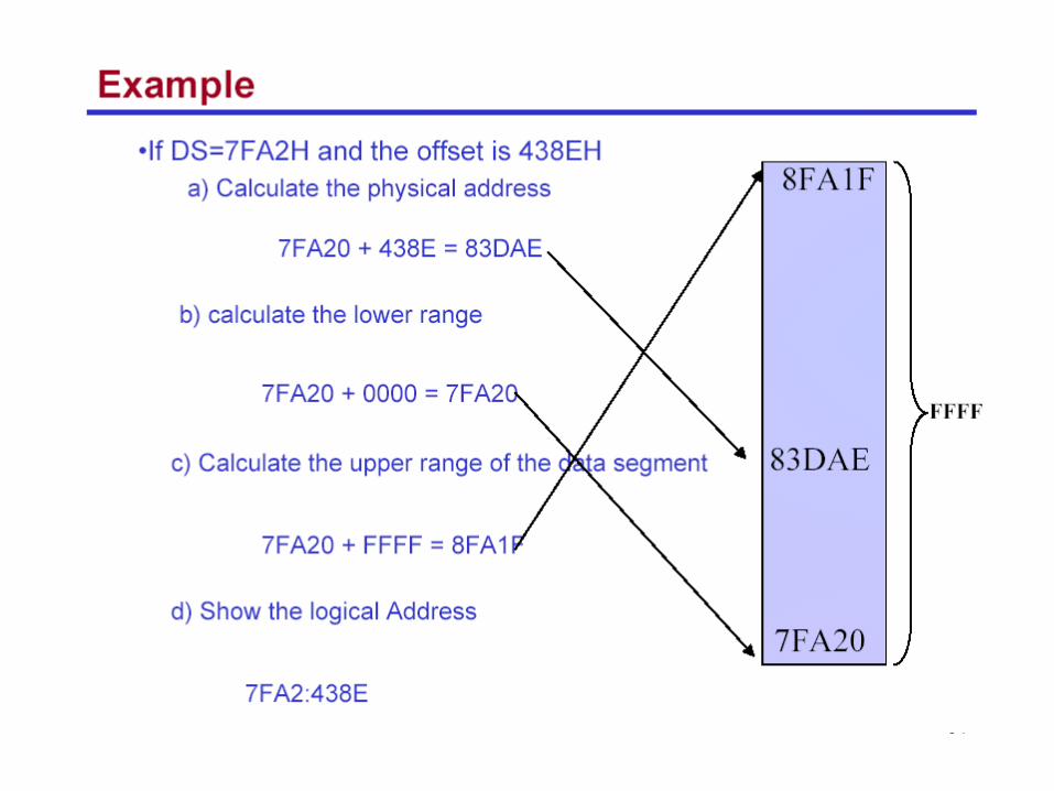
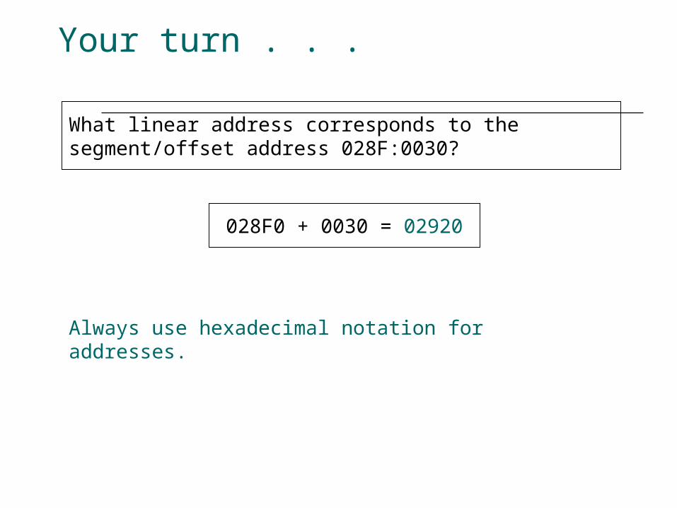
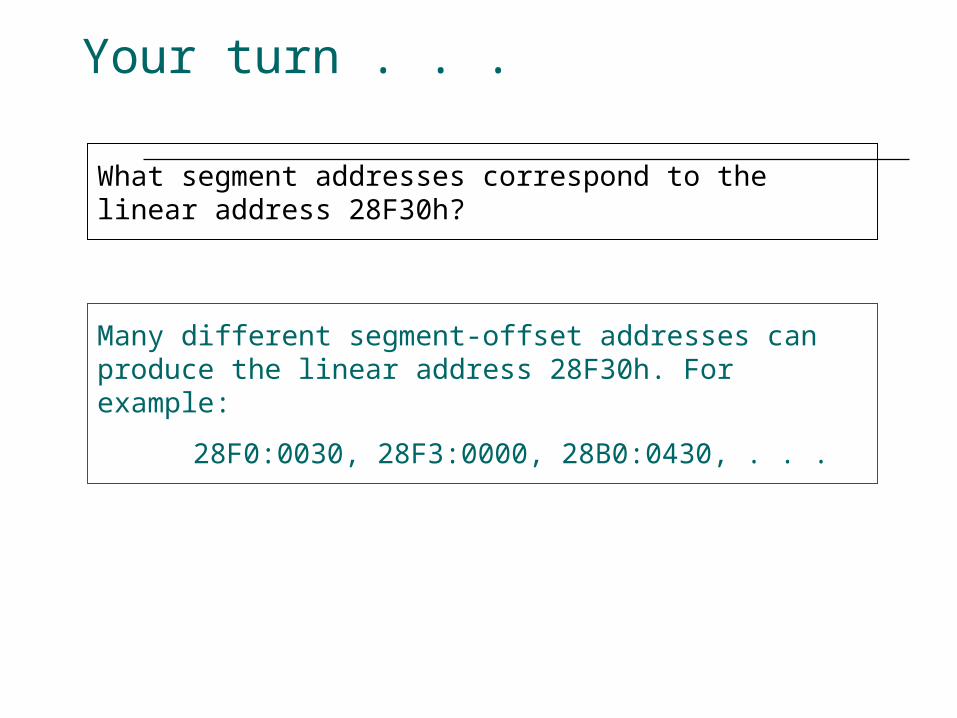
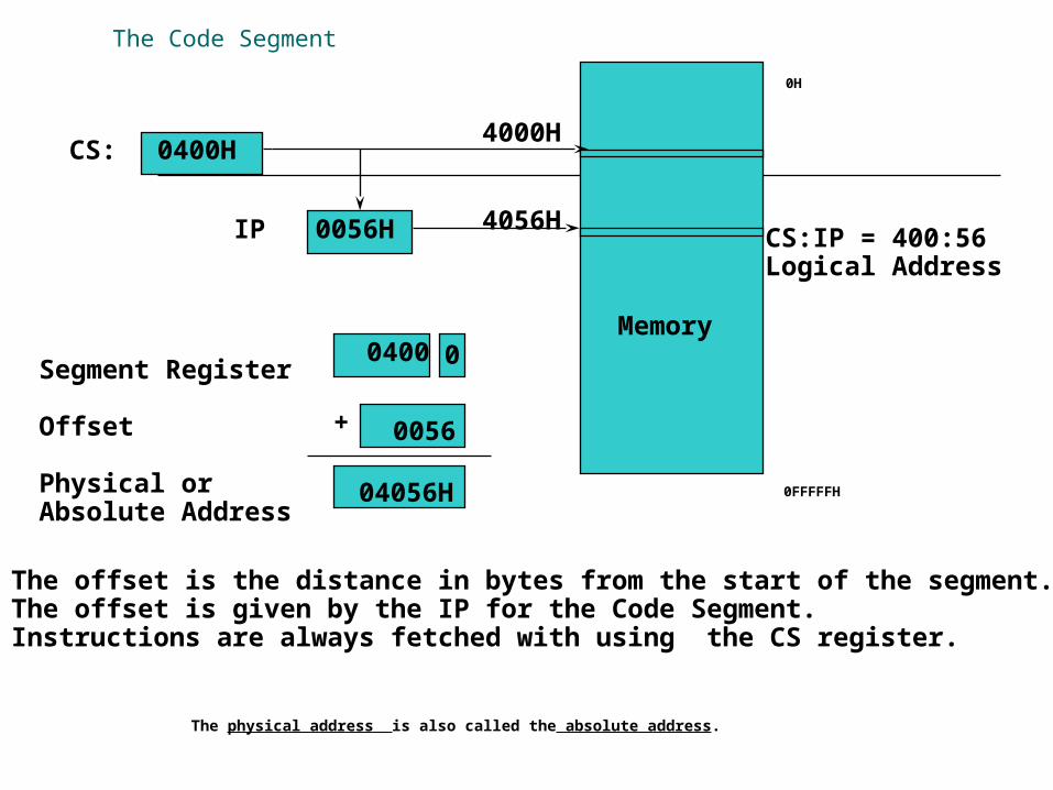
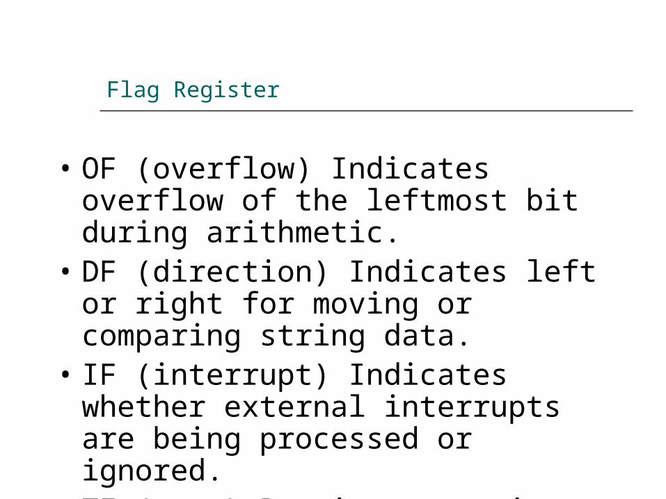
Minimum-Mode and Maximum-Mode System (cont)
Signals common to both minimum and maximum mode
Minimum-Mode and Maximum-Mode System (cont)
Unique minimum-mode signals
Minimum-Mode and Maximum-Mode System (cont)
Unique maximum-mode signals
Minimum-Mode and Maximum-Mode System (cont)
Minimum-Mode Interface
Block diagram of the minimum-mode 8088 MPU
Minimum-Mode Interface (cont)
Block diagram of the minimum-mode 8086 MPU
Minimum-Mode Interface (cont)
The minimum-mode signals can be divided into the following basic groups AddressData bus Status signals Control signals Interrupt signals DMA interface signals
Minimum-Mode Interface (cont)
AddressData bus The address bus is used to carry address information to
the memory and IO ports The address bus is 20-bit long and consists of signal lines
A0 through A19
A 20-bit address gives the 8088 a 1 Mbyte memory address space
Only address line A0 through A15 are used when addressing IO
This give an IO address space of 64 Kbytes The 8088 has 8 multiplexed addressdata bus lines
(A0~A7)
8086 has 16 multiplexed addressdata bus lines (A0~A15)
Minimum-Mode Interface (cont)
Status signals The four most significant address A19 through A16
are multiplexed with status signal S6 through S3
Bits S4 and S3 together form a 2-bit binary code that identifies which of the internal segment registers was used to generate the physical address
S5 is the logic level of the internal interrupt flag S6 is always at the 0 logic level
Minimum-Mode Interface (cont)
Minimum-Mode Interface (cont)
Minimum-Mode Interface (cont)
Maximum-Mode Interface
The maximum-mode configuration is mainly used for implementing a multiprocessorcoprocessor system environment Multiple processors exist in the system Each executes its own program
Global resources and local resources The former are common to all processors The latter are assigned to specific processors
In the maximum-mode facilities are provided for implementing allocation of global resources and passing bus control to other microprocessors sharing the system bus
Maximum-Mode Interface (cont)
8088 maximum-mode block diagram
Maximum-Mode Interface (cont)
8086 maximum-mode block diagram
Maximum-Mode Interface (cont)
8288 bus controller
Block diagram and pin layout of 8288
Maximum-Mode Interface (cont)
8288 bus controller In the maximum-mode 80888086 outputs a
status code on three signal line S0 S1 S2 prior to the initialization of each bus cycle
The 3-bit bus status code identifies which type of bus cycle is to follow and are input to the external bus controller device 8288
The 8288 produces one or two command signals for each bus cycle
Maximum-Mode Interface (cont)
8288 bus controller
Bus status code
Maximum-Mode Interface (cont)
Maximum-Mode Interface (cont)
Maximum-Mode Interface (cont)
Queue status signals The 2-bit queue status code QS0 and QS1 tells
the external circuitry what type of information was removed form the queue during the previous clock cycle
Queue status code
Electrical Characteristics
Power is applied between pin 40 (Vcc) and pins 1 (GND) and 20 (GND)
The nominal value of Vcc is specified as +5V dc with a tolerance of plusmn10
Both 8088 and 8086 draw a maximum of 340mA from the supply
IO voltage levels
System Clock
The time base for synchronization of the internal and external operations of the microprocessor in a microcomputer system is provided by the clock (CLK) input signal The standard 8088 operates at 5 MHz and the
8088-2 operates at 8 MHz The 8086 is manufactured in three speeds 5-
MHz 8086 8-MHz 8086-2 and the 10-MHz 8086-1
The CLK is externally generated by the 8284 clock generator and driver IC
System Clock (cont)
Block diagram of the 8284 clock generator
System Clock (cont)
Block diagram of the 8284 clock generator
System Clock (cont)
Connecting the 8284 to the 8088
15- or 24MHzcrystal
Typical value of CL when used with 15MHz crystal is 12pF
The fundamental crystal frequency is divided by 3 within the 8284 to give either a 5- or 8-MHz clock signal
System Clock (cont)
CLK waveform The signal is specified at Metal Oxide
Semiconductor (MOS)-compatible voltage level The period of the 5-MHz 8088 can range from
200 ns to 500 ns and the maximum rise and fall times of its edges equal 10 ns
System Clock (cont)
PCLK and OSC signals The peripheral clock (PCLK) and oscillator clock
(OSC) signals are provided to drive peripheral ICs The clock output at PCLK is half the frequency of
CLK The OSC output is at the crystal frequency which is three times of CLK
System Clock (cont)
The 8284 can also be driven from an external clock source Applied to the EFI (External Frequency Input) Input FC is used for selection
0 crystal between X1 and X2 is used 1 selects EFI
The CSYNC input is used for external synchronization in systems with multiple clocks
System Clock (cont)
EXAMPLE If the CLK input of an 8086 MPU is to be driven by
a 9-MHz signal what speed version of the 8086 must be used and what frequency crystal must be attached to the 8284
Solution The 8086-1 is the version of the 8086 that can be
run at 9-MHz To create the 9-MHz clock a 27-MHz crystal must be used on the 8284
Bus Cycle and Time States
A bus cycle defines the basic operation that a microprocessor performs to communicate with external devices
Examples of bus cycles are the memory read memory write inputoutput read and inputoutput write
The bus cycle of the 8088 and 8086 microprocessors consists of at least four clock periods
If no bus cycles are required the microprocessor performs what are known as idle states
When READY is held at the 0 level wait states are inserted between states T3 and T4 of the bus cycle
Bus Cycle and Time States (cont)
Bus cycle clock periods idle state and wait state
Bus Cycle and Time States (cont)
EXAMPLE What is the duration of the bus cycle in the 8088-
based microcomputer if the clock is 8 MHz and the two wait states are inserted
Solution The duration of the bus cycle in an 8 MHz system
is given by tcyc = 500 ns + N x 125 ns
In this expression the N stands for the number of waits states For a bus cycle with two wait states we get
tcyc = 500 ns + 2 x 125 ns = 500 ns + 250 ns = 750 ns
Hardware Organization of the Memory Address Space
1Mx8 memory bank of the 8088
Hardware Organization of the Memory Address Space (cont)
High and low memory banks of the 8086
Hardware Organization of the Memory Address Space (cont)
Byte transfer by the 8088
Hardware Organization of the Memory Address Space (cont)
Word transfer by the 8088
Hardware Organization of the Memory Address Space (cont)
Even address byte transfer by the 8086
Hardware Organization of the Memory Address Space (cont)
Odd address byte transfer by the 8086
Hardware Organization of the Memory Address Space (cont)
Even address word transfer by the 8086
Hardware Organization of the Memory Address Space (cont)
Odd-address word transfer by the 8086
Hardware Organization of the Memory Address Space (cont)
EXAMPLE Is the word at memory address 0123116 of an
8086-based microcomputer aligned or misaligned How many cycle are required to read it from memory
Solution The first byte of the word is the second byte at
the aligned-word address 0123016 Therefore the word is misaligned and required two bus cycles to be read from memory
Address Bus Status Codes
Whenever a memory bus cycle is in progress an address bus status code S4S3 is output by the processor S4S3 identifies which one of the four segment
register is used to generate the physical address in the current bus cycle 1048729
S4S3=00 identifies the extra segment register (ES)
S4S3=01 identifies the stack segment register (SS)
S4S3=10 identifies the code segment register (CS)
S4S3=11 identifies the data segment register (DS)
The memory address reach of the microprocessor can thus be expanded to 4 Mbytes
Memory Control Signals
Minimum-mode memory control signals
Memory Control Signals (cont)
Minimum-mode memory control signals (8088) ALE ndash Address Latch Enable ndash used to latch
the address in external memory IOM ndash Input-OutputMemory ndash signal external
circuitry whether a memory of IO bus cycle is in progress
DTR ndash Data TransmitReceive ndash signal external circuitry whether the 8088 is transmitting or receiving data over the bus 1048729
RD ndash Read ndash identifies that a read bus cycle is in progress
WR ndash Write ndash identifies that a write bus cycle is in progress
DEN ndash Data Enable ndash used to enable the data bus 1048729
SSO ndash Status Line ndash identifies whether a code or data access is in progress
Memory Control Signals (cont)
The control signals for the 8086rsquos minimum-mode memory interface differs in three ways IOM signal is replaced by MIO signal The signal SSO is removed from the interface BHE (bank high enable) is added to the interface
and is used to select input for the high bank of memory in the 8086rsquos memory subsystem
Memory Control Signals (cont)
Maximum-mode memory control signals
Memory Control Signals (cont)
Maximum-mode memory control signals MRDC ndash Memory Read Command 1048729 MWTC ndash Memory Write Command 1048729 AMWC ndash Advanced Memory Write Command
Read and Write Bus Cycle
Read cycle
Minimum-mode memory read bus cycle of the 8088
Read and Write Bus Cycle (cont)
Read cycle
Minimum-mode memory read bus cycle of the 8086
Read and Write Bus Cycle (cont)
Read cycle
Maximum-mode memory read bus cycle of the 8086
Read and Write Bus Cycle (cont)
Write cycle
Minimum-mode memory write bus cycle of the 8088
Read and Write Bus Cycle (cont)
Write cycle
Maximum-mode memory write bus cycle of the 8086
Memory Interface Circuit
Address bus latches and buffers Bank write and bank read control logic Data bus transceiversbuffers Address decoders
Memory Interface Circuit (cont)
Memory interface block diagram
Memory Interface Circuit (cont)
Address bus latches and buffers
Block diagram of a D-type latch
Memory Interface Circuit (cont)
Address bus latches and buffers
Circuit diagram of the 74F373
Memory Interface Circuit (cont)
A review of flip-floplatch logic
Positive edge-triggered D flip-flop
Memory Interface Circuit (cont)
A review of flip-floplatch logic
Positive edge-triggered JK flip-flop
Memory Interface Circuit (cont)
A review of flip-floplatch logic
D-type latch
Memory Interface Circuit (cont)
Address bus latches and buffers
Address latch circuit
Memory Interface Circuit (cont)
Bank write and bank read control logic
Bank write control logic Bank read control logic
Memory Interface Circuit (cont)
Data bus transceivers
Block diagram and circuit diagram of the 74F245 octal bus transceiver
Memory Interface Circuit (cont)
Data bus transceivers
Data bus transceiver circuit
Memory Interface Circuit (cont)
Address decoder
Address bus configuration with address decoding
Memory Interface Circuit (cont)
Address decoder
Block diagram and operation of the 74F139 decoder
Memory Interface Circuit (cont)
Address decoder
Circuit diagram of the 74F139 decoder
Memory Interface Circuit (cont)
Address decoder
Address decoder circuit using 74F139
Memory Interface Circuit (cont)
Address decoder
Block diagram and operation of the 74F138 decoder
Memory Interface Circuit (cont)
Address decoder
Circuit diagram of the 74F138 decoder
Memory Interface Circuit (cont)
Address decoder
Address decoder circuit using 74F138
Types of InputOutput
The IO system allows peripherals to provide data or receive results of processing the data Using IO ports
The 80888086 MPU can employ two types of IO Isolated IO Memory-mapped IO
They differ in how IO ports are mapped into the address space
Types of InputOutput (cont)
Isolated inputoutput When using isolated IO in a microcomputer
system the IO device are treated separate from memory
The memory address space contains 1 M consecutive byte address in the range 0000016 through FFFFF16
The IO address space contains 64K consecutive byte addresses in the range 000016 through FFFF16
The bytes in two consecutive IO addresses can be accessed as word-wide data
Page 0 000016 00FF16
Certain IO instructions can only perform in this range
Types of InputOutput (cont)
Isolated inputoutput
80888086 memory and IO address spaces
Types of InputOutput (cont)
Isolated inputoutput
Isolated IO ports
Types of InputOutput (cont)
Isolated inputoutput Advantages
The complete 1Mbyte memory address space is available for use with memory
Special instructions have been provided to perform IO operations with maximized performance
The bytes in two consecutive IO addresses can be accessed as word-wide data
Disadvantages All input and output data transfers must take place
between the AL or AX register and IO port
Types of InputOutput (cont)
Memory-mapped inputoutput MPU looks at the IO port as though it is a storage
location in memory Some of the memory address space is dedicated to IO
ports Instructions that affect data in memory are used
instead of the special IO instructions More instructions and addressing modes are available to
perform IO operations IO transfers can take place between IO port and other
internal registers The memory instructions tend to execute slower
than those specifically designed for isolated IO Part of the memory address space is lost
Types of InputOutput(cont)
Memory-mapped inputoutput
Memory mapped IO ports
Isolated InputOutput Interface
IO devices Keyboard Printer Mouse 82C55A etc
Functions of interface circuit Select the IO port Latch output data Sample input data Synchronize data transfer Translate between TTL voltage levels and those
required to operate the IO devices
Isolated InputOutput Interface (cont)
Minimum-mode interface
Minimum-mode 8088 system IO interface
Isolated InputOutput Interface (cont)
Minimum-mode interface
Minimum-mode 8086 system IO interface
Isolated InputOutput Interface (cont)
Maximum-mode interface
Maximum-mode 8088 system IO interface
Isolated InputOutput Interface (cont)
Maximum-mode interface
Maximum-mode 8086 system IO interface
Isolated InputOutput Interface (cont)
Maximum-mode interface
IO bus cycle status codes
InputOutput Data Transfer
Inputoutput data transfers in the 8088 and 8086 microcomputers can be either byte-wide or word-wide
IO addresses are 16 bits in length and are output by the 8088 to the IO interface over bus lines AD0 through AD7 and A8 through A15
In 8088 the word transfers is performed as two consecutive byte-wide data transfer and takes two bus cycle
In 8086 the word transfers can takes either one or two bus cycle
Word-wide IO ports should be aligned at even-address boundaries
InputOutput Data Instructions
InputOutput Data Instructions(cont)
EXAMPLE Write a sequence of instructions that will output
the data FF16 to a byte-wide output port at address AB16 of the IO address space
Solution First the AL register is loaded with FF16 as an
immediate operand in the instruction
MOV AL 0FFH Now the data in AL can be output to the byte-
wide output port with the instruction
OUT 0ABH AL
InputOutput Data Instructions(cont)
EXAMPLE Write a series of instructions that will output FF16 to an
output port located at address B00016 of the IO address space
Solution The DX register must first be loaded with the address
of the output port This is done with the instructionMOV DX 0B000H
Next the data that are to be output must be loaded into AL with the instruction
MOV AL 0FFH Finally the data are output with the instruction
OUT DX AL
InputOutput Data Instructions(cont)
EXAMPLE Data are to be read in from two byte-wide input
ports at addresses AA16 and A916 and then output as a word-wide output port at address B00016 Write a sequence of instructions to perform this inputoutput operation
InputOutput Data Instructions(cont)
Solution First read in the byte at address AA16 into AL and
move it into AHIN AL 0AAHMOV AH AL
Now the other byte can be read into AL by the instructionIN AL 09AH
And to write out the word of dataMOV DX 0B000HOUT DX AX
InputOutput Bus Cycles
Input bus cycle of the 8088
InputOutput Bus Cycles (cont)
Output bus cycle of the 8088
InputOutput Bus Cycles (cont)
Input bus cycle of the 8086
InputOutput Bus Cycles (cont)
Output bus cycle of the 8086
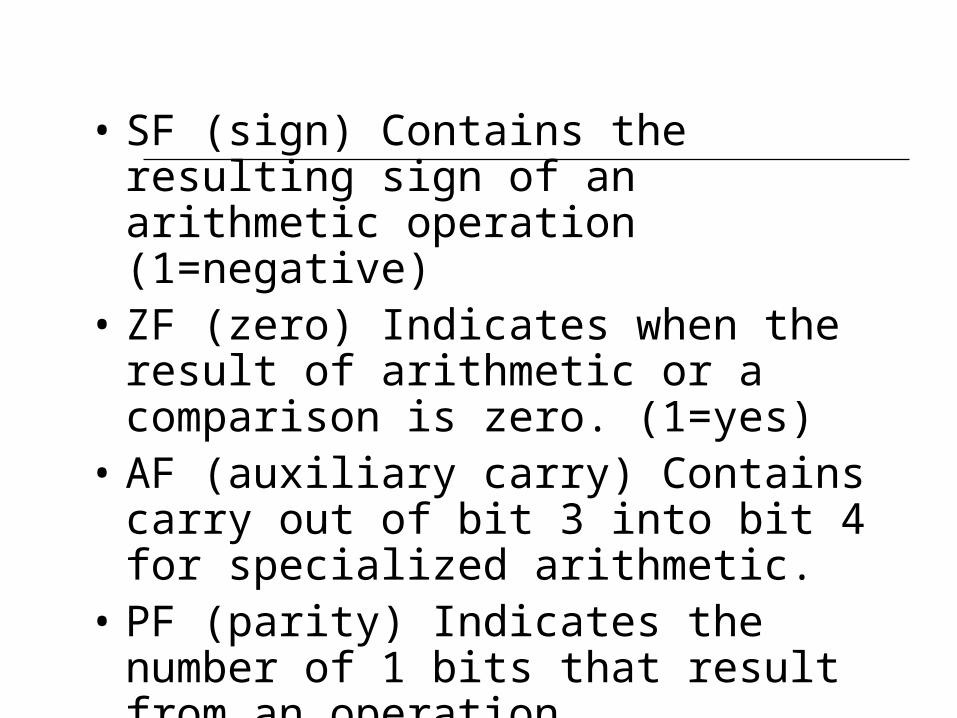
Minimum-Mode and Maximum-Mode System (cont)
Unique minimum-mode signals
Minimum-Mode and Maximum-Mode System (cont)
Unique maximum-mode signals
Minimum-Mode and Maximum-Mode System (cont)
Minimum-Mode Interface
Block diagram of the minimum-mode 8088 MPU
Minimum-Mode Interface (cont)
Block diagram of the minimum-mode 8086 MPU
Minimum-Mode Interface (cont)
The minimum-mode signals can be divided into the following basic groups AddressData bus Status signals Control signals Interrupt signals DMA interface signals
Minimum-Mode Interface (cont)
AddressData bus The address bus is used to carry address information to
the memory and IO ports The address bus is 20-bit long and consists of signal lines
A0 through A19
A 20-bit address gives the 8088 a 1 Mbyte memory address space
Only address line A0 through A15 are used when addressing IO
This give an IO address space of 64 Kbytes The 8088 has 8 multiplexed addressdata bus lines
(A0~A7)
8086 has 16 multiplexed addressdata bus lines (A0~A15)
Minimum-Mode Interface (cont)
Status signals The four most significant address A19 through A16
are multiplexed with status signal S6 through S3
Bits S4 and S3 together form a 2-bit binary code that identifies which of the internal segment registers was used to generate the physical address
S5 is the logic level of the internal interrupt flag S6 is always at the 0 logic level
Minimum-Mode Interface (cont)
Minimum-Mode Interface (cont)
Minimum-Mode Interface (cont)
Maximum-Mode Interface
The maximum-mode configuration is mainly used for implementing a multiprocessorcoprocessor system environment Multiple processors exist in the system Each executes its own program
Global resources and local resources The former are common to all processors The latter are assigned to specific processors
In the maximum-mode facilities are provided for implementing allocation of global resources and passing bus control to other microprocessors sharing the system bus
Maximum-Mode Interface (cont)
8088 maximum-mode block diagram
Maximum-Mode Interface (cont)
8086 maximum-mode block diagram
Maximum-Mode Interface (cont)
8288 bus controller
Block diagram and pin layout of 8288
Maximum-Mode Interface (cont)
8288 bus controller In the maximum-mode 80888086 outputs a
status code on three signal line S0 S1 S2 prior to the initialization of each bus cycle
The 3-bit bus status code identifies which type of bus cycle is to follow and are input to the external bus controller device 8288
The 8288 produces one or two command signals for each bus cycle
Maximum-Mode Interface (cont)
8288 bus controller
Bus status code
Maximum-Mode Interface (cont)
Maximum-Mode Interface (cont)
Maximum-Mode Interface (cont)
Queue status signals The 2-bit queue status code QS0 and QS1 tells
the external circuitry what type of information was removed form the queue during the previous clock cycle
Queue status code
Electrical Characteristics
Power is applied between pin 40 (Vcc) and pins 1 (GND) and 20 (GND)
The nominal value of Vcc is specified as +5V dc with a tolerance of plusmn10
Both 8088 and 8086 draw a maximum of 340mA from the supply
IO voltage levels
System Clock
The time base for synchronization of the internal and external operations of the microprocessor in a microcomputer system is provided by the clock (CLK) input signal The standard 8088 operates at 5 MHz and the
8088-2 operates at 8 MHz The 8086 is manufactured in three speeds 5-
MHz 8086 8-MHz 8086-2 and the 10-MHz 8086-1
The CLK is externally generated by the 8284 clock generator and driver IC
System Clock (cont)
Block diagram of the 8284 clock generator
System Clock (cont)
Block diagram of the 8284 clock generator
System Clock (cont)
Connecting the 8284 to the 8088
15- or 24MHzcrystal
Typical value of CL when used with 15MHz crystal is 12pF
The fundamental crystal frequency is divided by 3 within the 8284 to give either a 5- or 8-MHz clock signal
System Clock (cont)
CLK waveform The signal is specified at Metal Oxide
Semiconductor (MOS)-compatible voltage level The period of the 5-MHz 8088 can range from
200 ns to 500 ns and the maximum rise and fall times of its edges equal 10 ns
System Clock (cont)
PCLK and OSC signals The peripheral clock (PCLK) and oscillator clock
(OSC) signals are provided to drive peripheral ICs The clock output at PCLK is half the frequency of
CLK The OSC output is at the crystal frequency which is three times of CLK
System Clock (cont)
The 8284 can also be driven from an external clock source Applied to the EFI (External Frequency Input) Input FC is used for selection
0 crystal between X1 and X2 is used 1 selects EFI
The CSYNC input is used for external synchronization in systems with multiple clocks
System Clock (cont)
EXAMPLE If the CLK input of an 8086 MPU is to be driven by
a 9-MHz signal what speed version of the 8086 must be used and what frequency crystal must be attached to the 8284
Solution The 8086-1 is the version of the 8086 that can be
run at 9-MHz To create the 9-MHz clock a 27-MHz crystal must be used on the 8284
Bus Cycle and Time States
A bus cycle defines the basic operation that a microprocessor performs to communicate with external devices
Examples of bus cycles are the memory read memory write inputoutput read and inputoutput write
The bus cycle of the 8088 and 8086 microprocessors consists of at least four clock periods
If no bus cycles are required the microprocessor performs what are known as idle states
When READY is held at the 0 level wait states are inserted between states T3 and T4 of the bus cycle
Bus Cycle and Time States (cont)
Bus cycle clock periods idle state and wait state
Bus Cycle and Time States (cont)
EXAMPLE What is the duration of the bus cycle in the 8088-
based microcomputer if the clock is 8 MHz and the two wait states are inserted
Solution The duration of the bus cycle in an 8 MHz system
is given by tcyc = 500 ns + N x 125 ns
In this expression the N stands for the number of waits states For a bus cycle with two wait states we get
tcyc = 500 ns + 2 x 125 ns = 500 ns + 250 ns = 750 ns
Hardware Organization of the Memory Address Space
1Mx8 memory bank of the 8088
Hardware Organization of the Memory Address Space (cont)
High and low memory banks of the 8086
Hardware Organization of the Memory Address Space (cont)
Byte transfer by the 8088
Hardware Organization of the Memory Address Space (cont)
Word transfer by the 8088
Hardware Organization of the Memory Address Space (cont)
Even address byte transfer by the 8086
Hardware Organization of the Memory Address Space (cont)
Odd address byte transfer by the 8086
Hardware Organization of the Memory Address Space (cont)
Even address word transfer by the 8086
Hardware Organization of the Memory Address Space (cont)
Odd-address word transfer by the 8086
Hardware Organization of the Memory Address Space (cont)
EXAMPLE Is the word at memory address 0123116 of an
8086-based microcomputer aligned or misaligned How many cycle are required to read it from memory
Solution The first byte of the word is the second byte at
the aligned-word address 0123016 Therefore the word is misaligned and required two bus cycles to be read from memory
Address Bus Status Codes
Whenever a memory bus cycle is in progress an address bus status code S4S3 is output by the processor S4S3 identifies which one of the four segment
register is used to generate the physical address in the current bus cycle 1048729
S4S3=00 identifies the extra segment register (ES)
S4S3=01 identifies the stack segment register (SS)
S4S3=10 identifies the code segment register (CS)
S4S3=11 identifies the data segment register (DS)
The memory address reach of the microprocessor can thus be expanded to 4 Mbytes
Memory Control Signals
Minimum-mode memory control signals
Memory Control Signals (cont)
Minimum-mode memory control signals (8088) ALE ndash Address Latch Enable ndash used to latch
the address in external memory IOM ndash Input-OutputMemory ndash signal external
circuitry whether a memory of IO bus cycle is in progress
DTR ndash Data TransmitReceive ndash signal external circuitry whether the 8088 is transmitting or receiving data over the bus 1048729
RD ndash Read ndash identifies that a read bus cycle is in progress
WR ndash Write ndash identifies that a write bus cycle is in progress
DEN ndash Data Enable ndash used to enable the data bus 1048729
SSO ndash Status Line ndash identifies whether a code or data access is in progress
Memory Control Signals (cont)
The control signals for the 8086rsquos minimum-mode memory interface differs in three ways IOM signal is replaced by MIO signal The signal SSO is removed from the interface BHE (bank high enable) is added to the interface
and is used to select input for the high bank of memory in the 8086rsquos memory subsystem
Memory Control Signals (cont)
Maximum-mode memory control signals
Memory Control Signals (cont)
Maximum-mode memory control signals MRDC ndash Memory Read Command 1048729 MWTC ndash Memory Write Command 1048729 AMWC ndash Advanced Memory Write Command
Read and Write Bus Cycle
Read cycle
Minimum-mode memory read bus cycle of the 8088
Read and Write Bus Cycle (cont)
Read cycle
Minimum-mode memory read bus cycle of the 8086
Read and Write Bus Cycle (cont)
Read cycle
Maximum-mode memory read bus cycle of the 8086
Read and Write Bus Cycle (cont)
Write cycle
Minimum-mode memory write bus cycle of the 8088
Read and Write Bus Cycle (cont)
Write cycle
Maximum-mode memory write bus cycle of the 8086
Memory Interface Circuit
Address bus latches and buffers Bank write and bank read control logic Data bus transceiversbuffers Address decoders
Memory Interface Circuit (cont)
Memory interface block diagram
Memory Interface Circuit (cont)
Address bus latches and buffers
Block diagram of a D-type latch
Memory Interface Circuit (cont)
Address bus latches and buffers
Circuit diagram of the 74F373
Memory Interface Circuit (cont)
A review of flip-floplatch logic
Positive edge-triggered D flip-flop
Memory Interface Circuit (cont)
A review of flip-floplatch logic
Positive edge-triggered JK flip-flop
Memory Interface Circuit (cont)
A review of flip-floplatch logic
D-type latch
Memory Interface Circuit (cont)
Address bus latches and buffers
Address latch circuit
Memory Interface Circuit (cont)
Bank write and bank read control logic
Bank write control logic Bank read control logic
Memory Interface Circuit (cont)
Data bus transceivers
Block diagram and circuit diagram of the 74F245 octal bus transceiver
Memory Interface Circuit (cont)
Data bus transceivers
Data bus transceiver circuit
Memory Interface Circuit (cont)
Address decoder
Address bus configuration with address decoding
Memory Interface Circuit (cont)
Address decoder
Block diagram and operation of the 74F139 decoder
Memory Interface Circuit (cont)
Address decoder
Circuit diagram of the 74F139 decoder
Memory Interface Circuit (cont)
Address decoder
Address decoder circuit using 74F139
Memory Interface Circuit (cont)
Address decoder
Block diagram and operation of the 74F138 decoder
Memory Interface Circuit (cont)
Address decoder
Circuit diagram of the 74F138 decoder
Memory Interface Circuit (cont)
Address decoder
Address decoder circuit using 74F138
Types of InputOutput
The IO system allows peripherals to provide data or receive results of processing the data Using IO ports
The 80888086 MPU can employ two types of IO Isolated IO Memory-mapped IO
They differ in how IO ports are mapped into the address space
Types of InputOutput (cont)
Isolated inputoutput When using isolated IO in a microcomputer
system the IO device are treated separate from memory
The memory address space contains 1 M consecutive byte address in the range 0000016 through FFFFF16
The IO address space contains 64K consecutive byte addresses in the range 000016 through FFFF16
The bytes in two consecutive IO addresses can be accessed as word-wide data
Page 0 000016 00FF16
Certain IO instructions can only perform in this range
Types of InputOutput (cont)
Isolated inputoutput
80888086 memory and IO address spaces
Types of InputOutput (cont)
Isolated inputoutput
Isolated IO ports
Types of InputOutput (cont)
Isolated inputoutput Advantages
The complete 1Mbyte memory address space is available for use with memory
Special instructions have been provided to perform IO operations with maximized performance
The bytes in two consecutive IO addresses can be accessed as word-wide data
Disadvantages All input and output data transfers must take place
between the AL or AX register and IO port
Types of InputOutput (cont)
Memory-mapped inputoutput MPU looks at the IO port as though it is a storage
location in memory Some of the memory address space is dedicated to IO
ports Instructions that affect data in memory are used
instead of the special IO instructions More instructions and addressing modes are available to
perform IO operations IO transfers can take place between IO port and other
internal registers The memory instructions tend to execute slower
than those specifically designed for isolated IO Part of the memory address space is lost
Types of InputOutput(cont)
Memory-mapped inputoutput
Memory mapped IO ports
Isolated InputOutput Interface
IO devices Keyboard Printer Mouse 82C55A etc
Functions of interface circuit Select the IO port Latch output data Sample input data Synchronize data transfer Translate between TTL voltage levels and those
required to operate the IO devices
Isolated InputOutput Interface (cont)
Minimum-mode interface
Minimum-mode 8088 system IO interface
Isolated InputOutput Interface (cont)
Minimum-mode interface
Minimum-mode 8086 system IO interface
Isolated InputOutput Interface (cont)
Maximum-mode interface
Maximum-mode 8088 system IO interface
Isolated InputOutput Interface (cont)
Maximum-mode interface
Maximum-mode 8086 system IO interface
Isolated InputOutput Interface (cont)
Maximum-mode interface
IO bus cycle status codes
InputOutput Data Transfer
Inputoutput data transfers in the 8088 and 8086 microcomputers can be either byte-wide or word-wide
IO addresses are 16 bits in length and are output by the 8088 to the IO interface over bus lines AD0 through AD7 and A8 through A15
In 8088 the word transfers is performed as two consecutive byte-wide data transfer and takes two bus cycle
In 8086 the word transfers can takes either one or two bus cycle
Word-wide IO ports should be aligned at even-address boundaries
InputOutput Data Instructions
InputOutput Data Instructions(cont)
EXAMPLE Write a sequence of instructions that will output
the data FF16 to a byte-wide output port at address AB16 of the IO address space
Solution First the AL register is loaded with FF16 as an
immediate operand in the instruction
MOV AL 0FFH Now the data in AL can be output to the byte-
wide output port with the instruction
OUT 0ABH AL
InputOutput Data Instructions(cont)
EXAMPLE Write a series of instructions that will output FF16 to an
output port located at address B00016 of the IO address space
Solution The DX register must first be loaded with the address
of the output port This is done with the instructionMOV DX 0B000H
Next the data that are to be output must be loaded into AL with the instruction
MOV AL 0FFH Finally the data are output with the instruction
OUT DX AL
InputOutput Data Instructions(cont)
EXAMPLE Data are to be read in from two byte-wide input
ports at addresses AA16 and A916 and then output as a word-wide output port at address B00016 Write a sequence of instructions to perform this inputoutput operation
InputOutput Data Instructions(cont)
Solution First read in the byte at address AA16 into AL and
move it into AHIN AL 0AAHMOV AH AL
Now the other byte can be read into AL by the instructionIN AL 09AH
And to write out the word of dataMOV DX 0B000HOUT DX AX
InputOutput Bus Cycles
Input bus cycle of the 8088
InputOutput Bus Cycles (cont)
Output bus cycle of the 8088
InputOutput Bus Cycles (cont)
Input bus cycle of the 8086
InputOutput Bus Cycles (cont)
Output bus cycle of the 8086
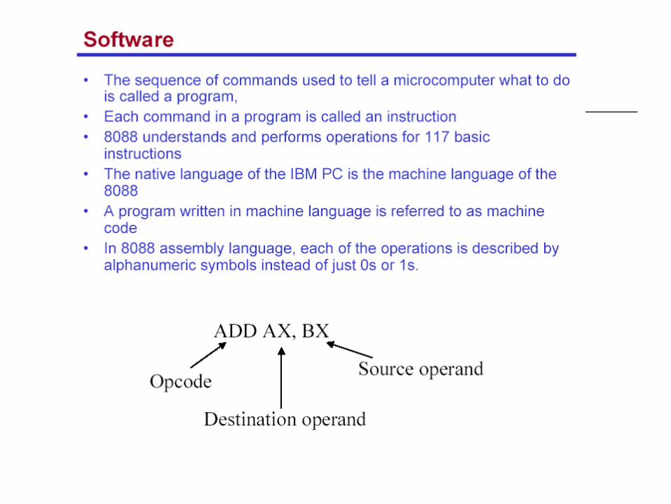
Minimum-Mode and Maximum-Mode System (cont)
Unique maximum-mode signals
Minimum-Mode and Maximum-Mode System (cont)
Minimum-Mode Interface
Block diagram of the minimum-mode 8088 MPU
Minimum-Mode Interface (cont)
Block diagram of the minimum-mode 8086 MPU
Minimum-Mode Interface (cont)
The minimum-mode signals can be divided into the following basic groups AddressData bus Status signals Control signals Interrupt signals DMA interface signals
Minimum-Mode Interface (cont)
AddressData bus The address bus is used to carry address information to
the memory and IO ports The address bus is 20-bit long and consists of signal lines
A0 through A19
A 20-bit address gives the 8088 a 1 Mbyte memory address space
Only address line A0 through A15 are used when addressing IO
This give an IO address space of 64 Kbytes The 8088 has 8 multiplexed addressdata bus lines
(A0~A7)
8086 has 16 multiplexed addressdata bus lines (A0~A15)
Minimum-Mode Interface (cont)
Status signals The four most significant address A19 through A16
are multiplexed with status signal S6 through S3
Bits S4 and S3 together form a 2-bit binary code that identifies which of the internal segment registers was used to generate the physical address
S5 is the logic level of the internal interrupt flag S6 is always at the 0 logic level
Minimum-Mode Interface (cont)
Minimum-Mode Interface (cont)
Minimum-Mode Interface (cont)
Maximum-Mode Interface
The maximum-mode configuration is mainly used for implementing a multiprocessorcoprocessor system environment Multiple processors exist in the system Each executes its own program
Global resources and local resources The former are common to all processors The latter are assigned to specific processors
In the maximum-mode facilities are provided for implementing allocation of global resources and passing bus control to other microprocessors sharing the system bus
Maximum-Mode Interface (cont)
8088 maximum-mode block diagram
Maximum-Mode Interface (cont)
8086 maximum-mode block diagram
Maximum-Mode Interface (cont)
8288 bus controller
Block diagram and pin layout of 8288
Maximum-Mode Interface (cont)
8288 bus controller In the maximum-mode 80888086 outputs a
status code on three signal line S0 S1 S2 prior to the initialization of each bus cycle
The 3-bit bus status code identifies which type of bus cycle is to follow and are input to the external bus controller device 8288
The 8288 produces one or two command signals for each bus cycle
Maximum-Mode Interface (cont)
8288 bus controller
Bus status code
Maximum-Mode Interface (cont)
Maximum-Mode Interface (cont)
Maximum-Mode Interface (cont)
Queue status signals The 2-bit queue status code QS0 and QS1 tells
the external circuitry what type of information was removed form the queue during the previous clock cycle
Queue status code
Electrical Characteristics
Power is applied between pin 40 (Vcc) and pins 1 (GND) and 20 (GND)
The nominal value of Vcc is specified as +5V dc with a tolerance of plusmn10
Both 8088 and 8086 draw a maximum of 340mA from the supply
IO voltage levels
System Clock
The time base for synchronization of the internal and external operations of the microprocessor in a microcomputer system is provided by the clock (CLK) input signal The standard 8088 operates at 5 MHz and the
8088-2 operates at 8 MHz The 8086 is manufactured in three speeds 5-
MHz 8086 8-MHz 8086-2 and the 10-MHz 8086-1
The CLK is externally generated by the 8284 clock generator and driver IC
System Clock (cont)
Block diagram of the 8284 clock generator
System Clock (cont)
Block diagram of the 8284 clock generator
System Clock (cont)
Connecting the 8284 to the 8088
15- or 24MHzcrystal
Typical value of CL when used with 15MHz crystal is 12pF
The fundamental crystal frequency is divided by 3 within the 8284 to give either a 5- or 8-MHz clock signal
System Clock (cont)
CLK waveform The signal is specified at Metal Oxide
Semiconductor (MOS)-compatible voltage level The period of the 5-MHz 8088 can range from
200 ns to 500 ns and the maximum rise and fall times of its edges equal 10 ns
System Clock (cont)
PCLK and OSC signals The peripheral clock (PCLK) and oscillator clock
(OSC) signals are provided to drive peripheral ICs The clock output at PCLK is half the frequency of
CLK The OSC output is at the crystal frequency which is three times of CLK
System Clock (cont)
The 8284 can also be driven from an external clock source Applied to the EFI (External Frequency Input) Input FC is used for selection
0 crystal between X1 and X2 is used 1 selects EFI
The CSYNC input is used for external synchronization in systems with multiple clocks
System Clock (cont)
EXAMPLE If the CLK input of an 8086 MPU is to be driven by
a 9-MHz signal what speed version of the 8086 must be used and what frequency crystal must be attached to the 8284
Solution The 8086-1 is the version of the 8086 that can be
run at 9-MHz To create the 9-MHz clock a 27-MHz crystal must be used on the 8284
Bus Cycle and Time States
A bus cycle defines the basic operation that a microprocessor performs to communicate with external devices
Examples of bus cycles are the memory read memory write inputoutput read and inputoutput write
The bus cycle of the 8088 and 8086 microprocessors consists of at least four clock periods
If no bus cycles are required the microprocessor performs what are known as idle states
When READY is held at the 0 level wait states are inserted between states T3 and T4 of the bus cycle
Bus Cycle and Time States (cont)
Bus cycle clock periods idle state and wait state
Bus Cycle and Time States (cont)
EXAMPLE What is the duration of the bus cycle in the 8088-
based microcomputer if the clock is 8 MHz and the two wait states are inserted
Solution The duration of the bus cycle in an 8 MHz system
is given by tcyc = 500 ns + N x 125 ns
In this expression the N stands for the number of waits states For a bus cycle with two wait states we get
tcyc = 500 ns + 2 x 125 ns = 500 ns + 250 ns = 750 ns
Hardware Organization of the Memory Address Space
1Mx8 memory bank of the 8088
Hardware Organization of the Memory Address Space (cont)
High and low memory banks of the 8086
Hardware Organization of the Memory Address Space (cont)
Byte transfer by the 8088
Hardware Organization of the Memory Address Space (cont)
Word transfer by the 8088
Hardware Organization of the Memory Address Space (cont)
Even address byte transfer by the 8086
Hardware Organization of the Memory Address Space (cont)
Odd address byte transfer by the 8086
Hardware Organization of the Memory Address Space (cont)
Even address word transfer by the 8086
Hardware Organization of the Memory Address Space (cont)
Odd-address word transfer by the 8086
Hardware Organization of the Memory Address Space (cont)
EXAMPLE Is the word at memory address 0123116 of an
8086-based microcomputer aligned or misaligned How many cycle are required to read it from memory
Solution The first byte of the word is the second byte at
the aligned-word address 0123016 Therefore the word is misaligned and required two bus cycles to be read from memory
Address Bus Status Codes
Whenever a memory bus cycle is in progress an address bus status code S4S3 is output by the processor S4S3 identifies which one of the four segment
register is used to generate the physical address in the current bus cycle 1048729
S4S3=00 identifies the extra segment register (ES)
S4S3=01 identifies the stack segment register (SS)
S4S3=10 identifies the code segment register (CS)
S4S3=11 identifies the data segment register (DS)
The memory address reach of the microprocessor can thus be expanded to 4 Mbytes
Memory Control Signals
Minimum-mode memory control signals
Memory Control Signals (cont)
Minimum-mode memory control signals (8088) ALE ndash Address Latch Enable ndash used to latch
the address in external memory IOM ndash Input-OutputMemory ndash signal external
circuitry whether a memory of IO bus cycle is in progress
DTR ndash Data TransmitReceive ndash signal external circuitry whether the 8088 is transmitting or receiving data over the bus 1048729
RD ndash Read ndash identifies that a read bus cycle is in progress
WR ndash Write ndash identifies that a write bus cycle is in progress
DEN ndash Data Enable ndash used to enable the data bus 1048729
SSO ndash Status Line ndash identifies whether a code or data access is in progress
Memory Control Signals (cont)
The control signals for the 8086rsquos minimum-mode memory interface differs in three ways IOM signal is replaced by MIO signal The signal SSO is removed from the interface BHE (bank high enable) is added to the interface
and is used to select input for the high bank of memory in the 8086rsquos memory subsystem
Memory Control Signals (cont)
Maximum-mode memory control signals
Memory Control Signals (cont)
Maximum-mode memory control signals MRDC ndash Memory Read Command 1048729 MWTC ndash Memory Write Command 1048729 AMWC ndash Advanced Memory Write Command
Read and Write Bus Cycle
Read cycle
Minimum-mode memory read bus cycle of the 8088
Read and Write Bus Cycle (cont)
Read cycle
Minimum-mode memory read bus cycle of the 8086
Read and Write Bus Cycle (cont)
Read cycle
Maximum-mode memory read bus cycle of the 8086
Read and Write Bus Cycle (cont)
Write cycle
Minimum-mode memory write bus cycle of the 8088
Read and Write Bus Cycle (cont)
Write cycle
Maximum-mode memory write bus cycle of the 8086
Memory Interface Circuit
Address bus latches and buffers Bank write and bank read control logic Data bus transceiversbuffers Address decoders
Memory Interface Circuit (cont)
Memory interface block diagram
Memory Interface Circuit (cont)
Address bus latches and buffers
Block diagram of a D-type latch
Memory Interface Circuit (cont)
Address bus latches and buffers
Circuit diagram of the 74F373
Memory Interface Circuit (cont)
A review of flip-floplatch logic
Positive edge-triggered D flip-flop
Memory Interface Circuit (cont)
A review of flip-floplatch logic
Positive edge-triggered JK flip-flop
Memory Interface Circuit (cont)
A review of flip-floplatch logic
D-type latch
Memory Interface Circuit (cont)
Address bus latches and buffers
Address latch circuit
Memory Interface Circuit (cont)
Bank write and bank read control logic
Bank write control logic Bank read control logic
Memory Interface Circuit (cont)
Data bus transceivers
Block diagram and circuit diagram of the 74F245 octal bus transceiver
Memory Interface Circuit (cont)
Data bus transceivers
Data bus transceiver circuit
Memory Interface Circuit (cont)
Address decoder
Address bus configuration with address decoding
Memory Interface Circuit (cont)
Address decoder
Block diagram and operation of the 74F139 decoder
Memory Interface Circuit (cont)
Address decoder
Circuit diagram of the 74F139 decoder
Memory Interface Circuit (cont)
Address decoder
Address decoder circuit using 74F139
Memory Interface Circuit (cont)
Address decoder
Block diagram and operation of the 74F138 decoder
Memory Interface Circuit (cont)
Address decoder
Circuit diagram of the 74F138 decoder
Memory Interface Circuit (cont)
Address decoder
Address decoder circuit using 74F138
Types of InputOutput
The IO system allows peripherals to provide data or receive results of processing the data Using IO ports
The 80888086 MPU can employ two types of IO Isolated IO Memory-mapped IO
They differ in how IO ports are mapped into the address space
Types of InputOutput (cont)
Isolated inputoutput When using isolated IO in a microcomputer
system the IO device are treated separate from memory
The memory address space contains 1 M consecutive byte address in the range 0000016 through FFFFF16
The IO address space contains 64K consecutive byte addresses in the range 000016 through FFFF16
The bytes in two consecutive IO addresses can be accessed as word-wide data
Page 0 000016 00FF16
Certain IO instructions can only perform in this range
Types of InputOutput (cont)
Isolated inputoutput
80888086 memory and IO address spaces
Types of InputOutput (cont)
Isolated inputoutput
Isolated IO ports
Types of InputOutput (cont)
Isolated inputoutput Advantages
The complete 1Mbyte memory address space is available for use with memory
Special instructions have been provided to perform IO operations with maximized performance
The bytes in two consecutive IO addresses can be accessed as word-wide data
Disadvantages All input and output data transfers must take place
between the AL or AX register and IO port
Types of InputOutput (cont)
Memory-mapped inputoutput MPU looks at the IO port as though it is a storage
location in memory Some of the memory address space is dedicated to IO
ports Instructions that affect data in memory are used
instead of the special IO instructions More instructions and addressing modes are available to
perform IO operations IO transfers can take place between IO port and other
internal registers The memory instructions tend to execute slower
than those specifically designed for isolated IO Part of the memory address space is lost
Types of InputOutput(cont)
Memory-mapped inputoutput
Memory mapped IO ports
Isolated InputOutput Interface
IO devices Keyboard Printer Mouse 82C55A etc
Functions of interface circuit Select the IO port Latch output data Sample input data Synchronize data transfer Translate between TTL voltage levels and those
required to operate the IO devices
Isolated InputOutput Interface (cont)
Minimum-mode interface
Minimum-mode 8088 system IO interface
Isolated InputOutput Interface (cont)
Minimum-mode interface
Minimum-mode 8086 system IO interface
Isolated InputOutput Interface (cont)
Maximum-mode interface
Maximum-mode 8088 system IO interface
Isolated InputOutput Interface (cont)
Maximum-mode interface
Maximum-mode 8086 system IO interface
Isolated InputOutput Interface (cont)
Maximum-mode interface
IO bus cycle status codes
InputOutput Data Transfer
Inputoutput data transfers in the 8088 and 8086 microcomputers can be either byte-wide or word-wide
IO addresses are 16 bits in length and are output by the 8088 to the IO interface over bus lines AD0 through AD7 and A8 through A15
In 8088 the word transfers is performed as two consecutive byte-wide data transfer and takes two bus cycle
In 8086 the word transfers can takes either one or two bus cycle
Word-wide IO ports should be aligned at even-address boundaries
InputOutput Data Instructions
InputOutput Data Instructions(cont)
EXAMPLE Write a sequence of instructions that will output
the data FF16 to a byte-wide output port at address AB16 of the IO address space
Solution First the AL register is loaded with FF16 as an
immediate operand in the instruction
MOV AL 0FFH Now the data in AL can be output to the byte-
wide output port with the instruction
OUT 0ABH AL
InputOutput Data Instructions(cont)
EXAMPLE Write a series of instructions that will output FF16 to an
output port located at address B00016 of the IO address space
Solution The DX register must first be loaded with the address
of the output port This is done with the instructionMOV DX 0B000H
Next the data that are to be output must be loaded into AL with the instruction
MOV AL 0FFH Finally the data are output with the instruction
OUT DX AL
InputOutput Data Instructions(cont)
EXAMPLE Data are to be read in from two byte-wide input
ports at addresses AA16 and A916 and then output as a word-wide output port at address B00016 Write a sequence of instructions to perform this inputoutput operation
InputOutput Data Instructions(cont)
Solution First read in the byte at address AA16 into AL and
move it into AHIN AL 0AAHMOV AH AL
Now the other byte can be read into AL by the instructionIN AL 09AH
And to write out the word of dataMOV DX 0B000HOUT DX AX
InputOutput Bus Cycles
Input bus cycle of the 8088
InputOutput Bus Cycles (cont)
Output bus cycle of the 8088
InputOutput Bus Cycles (cont)
Input bus cycle of the 8086
InputOutput Bus Cycles (cont)
Output bus cycle of the 8086
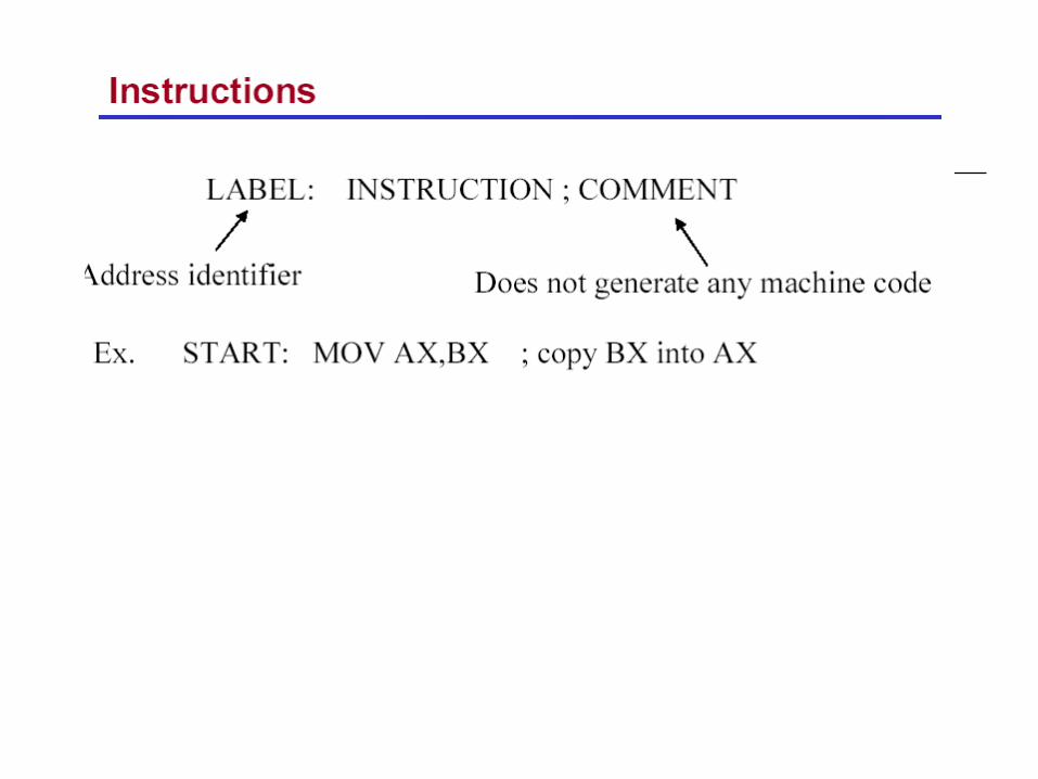
Minimum-Mode and Maximum-Mode System (cont)
Minimum-Mode Interface
Block diagram of the minimum-mode 8088 MPU
Minimum-Mode Interface (cont)
Block diagram of the minimum-mode 8086 MPU
Minimum-Mode Interface (cont)
The minimum-mode signals can be divided into the following basic groups AddressData bus Status signals Control signals Interrupt signals DMA interface signals
Minimum-Mode Interface (cont)
AddressData bus The address bus is used to carry address information to
the memory and IO ports The address bus is 20-bit long and consists of signal lines
A0 through A19
A 20-bit address gives the 8088 a 1 Mbyte memory address space
Only address line A0 through A15 are used when addressing IO
This give an IO address space of 64 Kbytes The 8088 has 8 multiplexed addressdata bus lines
(A0~A7)
8086 has 16 multiplexed addressdata bus lines (A0~A15)
Minimum-Mode Interface (cont)
Status signals The four most significant address A19 through A16
are multiplexed with status signal S6 through S3
Bits S4 and S3 together form a 2-bit binary code that identifies which of the internal segment registers was used to generate the physical address
S5 is the logic level of the internal interrupt flag S6 is always at the 0 logic level
Minimum-Mode Interface (cont)
Minimum-Mode Interface (cont)
Minimum-Mode Interface (cont)
Maximum-Mode Interface
The maximum-mode configuration is mainly used for implementing a multiprocessorcoprocessor system environment Multiple processors exist in the system Each executes its own program
Global resources and local resources The former are common to all processors The latter are assigned to specific processors
In the maximum-mode facilities are provided for implementing allocation of global resources and passing bus control to other microprocessors sharing the system bus
Maximum-Mode Interface (cont)
8088 maximum-mode block diagram
Maximum-Mode Interface (cont)
8086 maximum-mode block diagram
Maximum-Mode Interface (cont)
8288 bus controller
Block diagram and pin layout of 8288
Maximum-Mode Interface (cont)
8288 bus controller In the maximum-mode 80888086 outputs a
status code on three signal line S0 S1 S2 prior to the initialization of each bus cycle
The 3-bit bus status code identifies which type of bus cycle is to follow and are input to the external bus controller device 8288
The 8288 produces one or two command signals for each bus cycle
Maximum-Mode Interface (cont)
8288 bus controller
Bus status code
Maximum-Mode Interface (cont)
Maximum-Mode Interface (cont)
Maximum-Mode Interface (cont)
Queue status signals The 2-bit queue status code QS0 and QS1 tells
the external circuitry what type of information was removed form the queue during the previous clock cycle
Queue status code
Electrical Characteristics
Power is applied between pin 40 (Vcc) and pins 1 (GND) and 20 (GND)
The nominal value of Vcc is specified as +5V dc with a tolerance of plusmn10
Both 8088 and 8086 draw a maximum of 340mA from the supply
IO voltage levels
System Clock
The time base for synchronization of the internal and external operations of the microprocessor in a microcomputer system is provided by the clock (CLK) input signal The standard 8088 operates at 5 MHz and the
8088-2 operates at 8 MHz The 8086 is manufactured in three speeds 5-
MHz 8086 8-MHz 8086-2 and the 10-MHz 8086-1
The CLK is externally generated by the 8284 clock generator and driver IC
System Clock (cont)
Block diagram of the 8284 clock generator
System Clock (cont)
Block diagram of the 8284 clock generator
System Clock (cont)
Connecting the 8284 to the 8088
15- or 24MHzcrystal
Typical value of CL when used with 15MHz crystal is 12pF
The fundamental crystal frequency is divided by 3 within the 8284 to give either a 5- or 8-MHz clock signal
System Clock (cont)
CLK waveform The signal is specified at Metal Oxide
Semiconductor (MOS)-compatible voltage level The period of the 5-MHz 8088 can range from
200 ns to 500 ns and the maximum rise and fall times of its edges equal 10 ns
System Clock (cont)
PCLK and OSC signals The peripheral clock (PCLK) and oscillator clock
(OSC) signals are provided to drive peripheral ICs The clock output at PCLK is half the frequency of
CLK The OSC output is at the crystal frequency which is three times of CLK
System Clock (cont)
The 8284 can also be driven from an external clock source Applied to the EFI (External Frequency Input) Input FC is used for selection
0 crystal between X1 and X2 is used 1 selects EFI
The CSYNC input is used for external synchronization in systems with multiple clocks
System Clock (cont)
EXAMPLE If the CLK input of an 8086 MPU is to be driven by
a 9-MHz signal what speed version of the 8086 must be used and what frequency crystal must be attached to the 8284
Solution The 8086-1 is the version of the 8086 that can be
run at 9-MHz To create the 9-MHz clock a 27-MHz crystal must be used on the 8284
Bus Cycle and Time States
A bus cycle defines the basic operation that a microprocessor performs to communicate with external devices
Examples of bus cycles are the memory read memory write inputoutput read and inputoutput write
The bus cycle of the 8088 and 8086 microprocessors consists of at least four clock periods
If no bus cycles are required the microprocessor performs what are known as idle states
When READY is held at the 0 level wait states are inserted between states T3 and T4 of the bus cycle
Bus Cycle and Time States (cont)
Bus cycle clock periods idle state and wait state
Bus Cycle and Time States (cont)
EXAMPLE What is the duration of the bus cycle in the 8088-
based microcomputer if the clock is 8 MHz and the two wait states are inserted
Solution The duration of the bus cycle in an 8 MHz system
is given by tcyc = 500 ns + N x 125 ns
In this expression the N stands for the number of waits states For a bus cycle with two wait states we get
tcyc = 500 ns + 2 x 125 ns = 500 ns + 250 ns = 750 ns
Hardware Organization of the Memory Address Space
1Mx8 memory bank of the 8088
Hardware Organization of the Memory Address Space (cont)
High and low memory banks of the 8086
Hardware Organization of the Memory Address Space (cont)
Byte transfer by the 8088
Hardware Organization of the Memory Address Space (cont)
Word transfer by the 8088
Hardware Organization of the Memory Address Space (cont)
Even address byte transfer by the 8086
Hardware Organization of the Memory Address Space (cont)
Odd address byte transfer by the 8086
Hardware Organization of the Memory Address Space (cont)
Even address word transfer by the 8086
Hardware Organization of the Memory Address Space (cont)
Odd-address word transfer by the 8086
Hardware Organization of the Memory Address Space (cont)
EXAMPLE Is the word at memory address 0123116 of an
8086-based microcomputer aligned or misaligned How many cycle are required to read it from memory
Solution The first byte of the word is the second byte at
the aligned-word address 0123016 Therefore the word is misaligned and required two bus cycles to be read from memory
Address Bus Status Codes
Whenever a memory bus cycle is in progress an address bus status code S4S3 is output by the processor S4S3 identifies which one of the four segment
register is used to generate the physical address in the current bus cycle 1048729
S4S3=00 identifies the extra segment register (ES)
S4S3=01 identifies the stack segment register (SS)
S4S3=10 identifies the code segment register (CS)
S4S3=11 identifies the data segment register (DS)
The memory address reach of the microprocessor can thus be expanded to 4 Mbytes
Memory Control Signals
Minimum-mode memory control signals
Memory Control Signals (cont)
Minimum-mode memory control signals (8088) ALE ndash Address Latch Enable ndash used to latch
the address in external memory IOM ndash Input-OutputMemory ndash signal external
circuitry whether a memory of IO bus cycle is in progress
DTR ndash Data TransmitReceive ndash signal external circuitry whether the 8088 is transmitting or receiving data over the bus 1048729
RD ndash Read ndash identifies that a read bus cycle is in progress
WR ndash Write ndash identifies that a write bus cycle is in progress
DEN ndash Data Enable ndash used to enable the data bus 1048729
SSO ndash Status Line ndash identifies whether a code or data access is in progress
Memory Control Signals (cont)
The control signals for the 8086rsquos minimum-mode memory interface differs in three ways IOM signal is replaced by MIO signal The signal SSO is removed from the interface BHE (bank high enable) is added to the interface
and is used to select input for the high bank of memory in the 8086rsquos memory subsystem
Memory Control Signals (cont)
Maximum-mode memory control signals
Memory Control Signals (cont)
Maximum-mode memory control signals MRDC ndash Memory Read Command 1048729 MWTC ndash Memory Write Command 1048729 AMWC ndash Advanced Memory Write Command
Read and Write Bus Cycle
Read cycle
Minimum-mode memory read bus cycle of the 8088
Read and Write Bus Cycle (cont)
Read cycle
Minimum-mode memory read bus cycle of the 8086
Read and Write Bus Cycle (cont)
Read cycle
Maximum-mode memory read bus cycle of the 8086
Read and Write Bus Cycle (cont)
Write cycle
Minimum-mode memory write bus cycle of the 8088
Read and Write Bus Cycle (cont)
Write cycle
Maximum-mode memory write bus cycle of the 8086
Memory Interface Circuit
Address bus latches and buffers Bank write and bank read control logic Data bus transceiversbuffers Address decoders
Memory Interface Circuit (cont)
Memory interface block diagram
Memory Interface Circuit (cont)
Address bus latches and buffers
Block diagram of a D-type latch
Memory Interface Circuit (cont)
Address bus latches and buffers
Circuit diagram of the 74F373
Memory Interface Circuit (cont)
A review of flip-floplatch logic
Positive edge-triggered D flip-flop
Memory Interface Circuit (cont)
A review of flip-floplatch logic
Positive edge-triggered JK flip-flop
Memory Interface Circuit (cont)
A review of flip-floplatch logic
D-type latch
Memory Interface Circuit (cont)
Address bus latches and buffers
Address latch circuit
Memory Interface Circuit (cont)
Bank write and bank read control logic
Bank write control logic Bank read control logic
Memory Interface Circuit (cont)
Data bus transceivers
Block diagram and circuit diagram of the 74F245 octal bus transceiver
Memory Interface Circuit (cont)
Data bus transceivers
Data bus transceiver circuit
Memory Interface Circuit (cont)
Address decoder
Address bus configuration with address decoding
Memory Interface Circuit (cont)
Address decoder
Block diagram and operation of the 74F139 decoder
Memory Interface Circuit (cont)
Address decoder
Circuit diagram of the 74F139 decoder
Memory Interface Circuit (cont)
Address decoder
Address decoder circuit using 74F139
Memory Interface Circuit (cont)
Address decoder
Block diagram and operation of the 74F138 decoder
Memory Interface Circuit (cont)
Address decoder
Circuit diagram of the 74F138 decoder
Memory Interface Circuit (cont)
Address decoder
Address decoder circuit using 74F138
Types of InputOutput
The IO system allows peripherals to provide data or receive results of processing the data Using IO ports
The 80888086 MPU can employ two types of IO Isolated IO Memory-mapped IO
They differ in how IO ports are mapped into the address space
Types of InputOutput (cont)
Isolated inputoutput When using isolated IO in a microcomputer
system the IO device are treated separate from memory
The memory address space contains 1 M consecutive byte address in the range 0000016 through FFFFF16
The IO address space contains 64K consecutive byte addresses in the range 000016 through FFFF16
The bytes in two consecutive IO addresses can be accessed as word-wide data
Page 0 000016 00FF16
Certain IO instructions can only perform in this range
Types of InputOutput (cont)
Isolated inputoutput
80888086 memory and IO address spaces
Types of InputOutput (cont)
Isolated inputoutput
Isolated IO ports
Types of InputOutput (cont)
Isolated inputoutput Advantages
The complete 1Mbyte memory address space is available for use with memory
Special instructions have been provided to perform IO operations with maximized performance
The bytes in two consecutive IO addresses can be accessed as word-wide data
Disadvantages All input and output data transfers must take place
between the AL or AX register and IO port
Types of InputOutput (cont)
Memory-mapped inputoutput MPU looks at the IO port as though it is a storage
location in memory Some of the memory address space is dedicated to IO
ports Instructions that affect data in memory are used
instead of the special IO instructions More instructions and addressing modes are available to
perform IO operations IO transfers can take place between IO port and other
internal registers The memory instructions tend to execute slower
than those specifically designed for isolated IO Part of the memory address space is lost
Types of InputOutput(cont)
Memory-mapped inputoutput
Memory mapped IO ports
Isolated InputOutput Interface
IO devices Keyboard Printer Mouse 82C55A etc
Functions of interface circuit Select the IO port Latch output data Sample input data Synchronize data transfer Translate between TTL voltage levels and those
required to operate the IO devices
Isolated InputOutput Interface (cont)
Minimum-mode interface
Minimum-mode 8088 system IO interface
Isolated InputOutput Interface (cont)
Minimum-mode interface
Minimum-mode 8086 system IO interface
Isolated InputOutput Interface (cont)
Maximum-mode interface
Maximum-mode 8088 system IO interface
Isolated InputOutput Interface (cont)
Maximum-mode interface
Maximum-mode 8086 system IO interface
Isolated InputOutput Interface (cont)
Maximum-mode interface
IO bus cycle status codes
InputOutput Data Transfer
Inputoutput data transfers in the 8088 and 8086 microcomputers can be either byte-wide or word-wide
IO addresses are 16 bits in length and are output by the 8088 to the IO interface over bus lines AD0 through AD7 and A8 through A15
In 8088 the word transfers is performed as two consecutive byte-wide data transfer and takes two bus cycle
In 8086 the word transfers can takes either one or two bus cycle
Word-wide IO ports should be aligned at even-address boundaries
InputOutput Data Instructions
InputOutput Data Instructions(cont)
EXAMPLE Write a sequence of instructions that will output
the data FF16 to a byte-wide output port at address AB16 of the IO address space
Solution First the AL register is loaded with FF16 as an
immediate operand in the instruction
MOV AL 0FFH Now the data in AL can be output to the byte-
wide output port with the instruction
OUT 0ABH AL
InputOutput Data Instructions(cont)
EXAMPLE Write a series of instructions that will output FF16 to an
output port located at address B00016 of the IO address space
Solution The DX register must first be loaded with the address
of the output port This is done with the instructionMOV DX 0B000H
Next the data that are to be output must be loaded into AL with the instruction
MOV AL 0FFH Finally the data are output with the instruction
OUT DX AL
InputOutput Data Instructions(cont)
EXAMPLE Data are to be read in from two byte-wide input
ports at addresses AA16 and A916 and then output as a word-wide output port at address B00016 Write a sequence of instructions to perform this inputoutput operation
InputOutput Data Instructions(cont)
Solution First read in the byte at address AA16 into AL and
move it into AHIN AL 0AAHMOV AH AL
Now the other byte can be read into AL by the instructionIN AL 09AH
And to write out the word of dataMOV DX 0B000HOUT DX AX
InputOutput Bus Cycles
Input bus cycle of the 8088
InputOutput Bus Cycles (cont)
Output bus cycle of the 8088
InputOutput Bus Cycles (cont)
Input bus cycle of the 8086
InputOutput Bus Cycles (cont)
Output bus cycle of the 8086
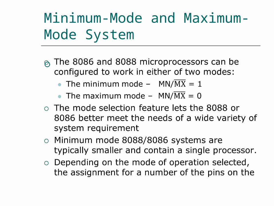
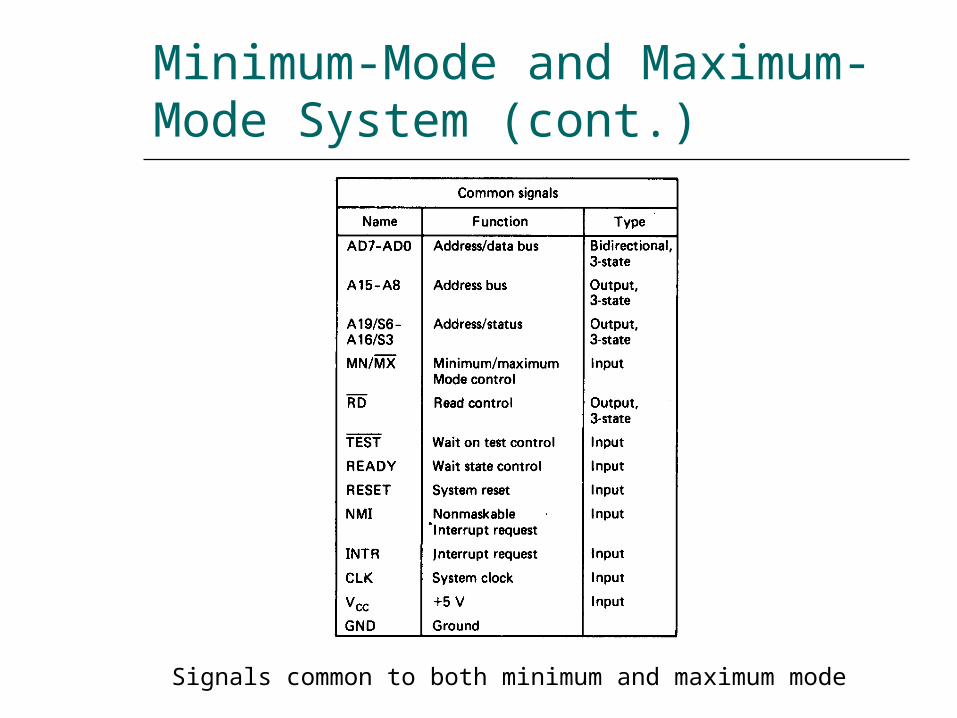
Minimum-Mode Interface (cont)
Block diagram of the minimum-mode 8086 MPU
Minimum-Mode Interface (cont)
The minimum-mode signals can be divided into the following basic groups AddressData bus Status signals Control signals Interrupt signals DMA interface signals
Minimum-Mode Interface (cont)
AddressData bus The address bus is used to carry address information to
the memory and IO ports The address bus is 20-bit long and consists of signal lines
A0 through A19
A 20-bit address gives the 8088 a 1 Mbyte memory address space
Only address line A0 through A15 are used when addressing IO
This give an IO address space of 64 Kbytes The 8088 has 8 multiplexed addressdata bus lines
(A0~A7)
8086 has 16 multiplexed addressdata bus lines (A0~A15)
Minimum-Mode Interface (cont)
Status signals The four most significant address A19 through A16
are multiplexed with status signal S6 through S3
Bits S4 and S3 together form a 2-bit binary code that identifies which of the internal segment registers was used to generate the physical address
S5 is the logic level of the internal interrupt flag S6 is always at the 0 logic level
Minimum-Mode Interface (cont)
Minimum-Mode Interface (cont)
Minimum-Mode Interface (cont)
Maximum-Mode Interface
The maximum-mode configuration is mainly used for implementing a multiprocessorcoprocessor system environment Multiple processors exist in the system Each executes its own program
Global resources and local resources The former are common to all processors The latter are assigned to specific processors
In the maximum-mode facilities are provided for implementing allocation of global resources and passing bus control to other microprocessors sharing the system bus
Maximum-Mode Interface (cont)
8088 maximum-mode block diagram
Maximum-Mode Interface (cont)
8086 maximum-mode block diagram
Maximum-Mode Interface (cont)
8288 bus controller
Block diagram and pin layout of 8288
Maximum-Mode Interface (cont)
8288 bus controller In the maximum-mode 80888086 outputs a
status code on three signal line S0 S1 S2 prior to the initialization of each bus cycle
The 3-bit bus status code identifies which type of bus cycle is to follow and are input to the external bus controller device 8288
The 8288 produces one or two command signals for each bus cycle
Maximum-Mode Interface (cont)
8288 bus controller
Bus status code
Maximum-Mode Interface (cont)
Maximum-Mode Interface (cont)
Maximum-Mode Interface (cont)
Queue status signals The 2-bit queue status code QS0 and QS1 tells
the external circuitry what type of information was removed form the queue during the previous clock cycle
Queue status code
Electrical Characteristics
Power is applied between pin 40 (Vcc) and pins 1 (GND) and 20 (GND)
The nominal value of Vcc is specified as +5V dc with a tolerance of plusmn10
Both 8088 and 8086 draw a maximum of 340mA from the supply
IO voltage levels
System Clock
The time base for synchronization of the internal and external operations of the microprocessor in a microcomputer system is provided by the clock (CLK) input signal The standard 8088 operates at 5 MHz and the
8088-2 operates at 8 MHz The 8086 is manufactured in three speeds 5-
MHz 8086 8-MHz 8086-2 and the 10-MHz 8086-1
The CLK is externally generated by the 8284 clock generator and driver IC
System Clock (cont)
Block diagram of the 8284 clock generator
System Clock (cont)
Block diagram of the 8284 clock generator
System Clock (cont)
Connecting the 8284 to the 8088
15- or 24MHzcrystal
Typical value of CL when used with 15MHz crystal is 12pF
The fundamental crystal frequency is divided by 3 within the 8284 to give either a 5- or 8-MHz clock signal
System Clock (cont)
CLK waveform The signal is specified at Metal Oxide
Semiconductor (MOS)-compatible voltage level The period of the 5-MHz 8088 can range from
200 ns to 500 ns and the maximum rise and fall times of its edges equal 10 ns
System Clock (cont)
PCLK and OSC signals The peripheral clock (PCLK) and oscillator clock
(OSC) signals are provided to drive peripheral ICs The clock output at PCLK is half the frequency of
CLK The OSC output is at the crystal frequency which is three times of CLK
System Clock (cont)
The 8284 can also be driven from an external clock source Applied to the EFI (External Frequency Input) Input FC is used for selection
0 crystal between X1 and X2 is used 1 selects EFI
The CSYNC input is used for external synchronization in systems with multiple clocks
System Clock (cont)
EXAMPLE If the CLK input of an 8086 MPU is to be driven by
a 9-MHz signal what speed version of the 8086 must be used and what frequency crystal must be attached to the 8284
Solution The 8086-1 is the version of the 8086 that can be
run at 9-MHz To create the 9-MHz clock a 27-MHz crystal must be used on the 8284
Bus Cycle and Time States
A bus cycle defines the basic operation that a microprocessor performs to communicate with external devices
Examples of bus cycles are the memory read memory write inputoutput read and inputoutput write
The bus cycle of the 8088 and 8086 microprocessors consists of at least four clock periods
If no bus cycles are required the microprocessor performs what are known as idle states
When READY is held at the 0 level wait states are inserted between states T3 and T4 of the bus cycle
Bus Cycle and Time States (cont)
Bus cycle clock periods idle state and wait state
Bus Cycle and Time States (cont)
EXAMPLE What is the duration of the bus cycle in the 8088-
based microcomputer if the clock is 8 MHz and the two wait states are inserted
Solution The duration of the bus cycle in an 8 MHz system
is given by tcyc = 500 ns + N x 125 ns
In this expression the N stands for the number of waits states For a bus cycle with two wait states we get
tcyc = 500 ns + 2 x 125 ns = 500 ns + 250 ns = 750 ns
Hardware Organization of the Memory Address Space
1Mx8 memory bank of the 8088
Hardware Organization of the Memory Address Space (cont)
High and low memory banks of the 8086
Hardware Organization of the Memory Address Space (cont)
Byte transfer by the 8088
Hardware Organization of the Memory Address Space (cont)
Word transfer by the 8088
Hardware Organization of the Memory Address Space (cont)
Even address byte transfer by the 8086
Hardware Organization of the Memory Address Space (cont)
Odd address byte transfer by the 8086
Hardware Organization of the Memory Address Space (cont)
Even address word transfer by the 8086
Hardware Organization of the Memory Address Space (cont)
Odd-address word transfer by the 8086
Hardware Organization of the Memory Address Space (cont)
EXAMPLE Is the word at memory address 0123116 of an
8086-based microcomputer aligned or misaligned How many cycle are required to read it from memory
Solution The first byte of the word is the second byte at
the aligned-word address 0123016 Therefore the word is misaligned and required two bus cycles to be read from memory
Address Bus Status Codes
Whenever a memory bus cycle is in progress an address bus status code S4S3 is output by the processor S4S3 identifies which one of the four segment
register is used to generate the physical address in the current bus cycle 1048729
S4S3=00 identifies the extra segment register (ES)
S4S3=01 identifies the stack segment register (SS)
S4S3=10 identifies the code segment register (CS)
S4S3=11 identifies the data segment register (DS)
The memory address reach of the microprocessor can thus be expanded to 4 Mbytes
Memory Control Signals
Minimum-mode memory control signals
Memory Control Signals (cont)
Minimum-mode memory control signals (8088) ALE ndash Address Latch Enable ndash used to latch
the address in external memory IOM ndash Input-OutputMemory ndash signal external
circuitry whether a memory of IO bus cycle is in progress
DTR ndash Data TransmitReceive ndash signal external circuitry whether the 8088 is transmitting or receiving data over the bus 1048729
RD ndash Read ndash identifies that a read bus cycle is in progress
WR ndash Write ndash identifies that a write bus cycle is in progress
DEN ndash Data Enable ndash used to enable the data bus 1048729
SSO ndash Status Line ndash identifies whether a code or data access is in progress
Memory Control Signals (cont)
The control signals for the 8086rsquos minimum-mode memory interface differs in three ways IOM signal is replaced by MIO signal The signal SSO is removed from the interface BHE (bank high enable) is added to the interface
and is used to select input for the high bank of memory in the 8086rsquos memory subsystem
Memory Control Signals (cont)
Maximum-mode memory control signals
Memory Control Signals (cont)
Maximum-mode memory control signals MRDC ndash Memory Read Command 1048729 MWTC ndash Memory Write Command 1048729 AMWC ndash Advanced Memory Write Command
Read and Write Bus Cycle
Read cycle
Minimum-mode memory read bus cycle of the 8088
Read and Write Bus Cycle (cont)
Read cycle
Minimum-mode memory read bus cycle of the 8086
Read and Write Bus Cycle (cont)
Read cycle
Maximum-mode memory read bus cycle of the 8086
Read and Write Bus Cycle (cont)
Write cycle
Minimum-mode memory write bus cycle of the 8088
Read and Write Bus Cycle (cont)
Write cycle
Maximum-mode memory write bus cycle of the 8086
Memory Interface Circuit
Address bus latches and buffers Bank write and bank read control logic Data bus transceiversbuffers Address decoders
Memory Interface Circuit (cont)
Memory interface block diagram
Memory Interface Circuit (cont)
Address bus latches and buffers
Block diagram of a D-type latch
Memory Interface Circuit (cont)
Address bus latches and buffers
Circuit diagram of the 74F373
Memory Interface Circuit (cont)
A review of flip-floplatch logic
Positive edge-triggered D flip-flop
Memory Interface Circuit (cont)
A review of flip-floplatch logic
Positive edge-triggered JK flip-flop
Memory Interface Circuit (cont)
A review of flip-floplatch logic
D-type latch
Memory Interface Circuit (cont)
Address bus latches and buffers
Address latch circuit
Memory Interface Circuit (cont)
Bank write and bank read control logic
Bank write control logic Bank read control logic
Memory Interface Circuit (cont)
Data bus transceivers
Block diagram and circuit diagram of the 74F245 octal bus transceiver
Memory Interface Circuit (cont)
Data bus transceivers
Data bus transceiver circuit
Memory Interface Circuit (cont)
Address decoder
Address bus configuration with address decoding
Memory Interface Circuit (cont)
Address decoder
Block diagram and operation of the 74F139 decoder
Memory Interface Circuit (cont)
Address decoder
Circuit diagram of the 74F139 decoder
Memory Interface Circuit (cont)
Address decoder
Address decoder circuit using 74F139
Memory Interface Circuit (cont)
Address decoder
Block diagram and operation of the 74F138 decoder
Memory Interface Circuit (cont)
Address decoder
Circuit diagram of the 74F138 decoder
Memory Interface Circuit (cont)
Address decoder
Address decoder circuit using 74F138
Types of InputOutput
The IO system allows peripherals to provide data or receive results of processing the data Using IO ports
The 80888086 MPU can employ two types of IO Isolated IO Memory-mapped IO
They differ in how IO ports are mapped into the address space
Types of InputOutput (cont)
Isolated inputoutput When using isolated IO in a microcomputer
system the IO device are treated separate from memory
The memory address space contains 1 M consecutive byte address in the range 0000016 through FFFFF16
The IO address space contains 64K consecutive byte addresses in the range 000016 through FFFF16
The bytes in two consecutive IO addresses can be accessed as word-wide data
Page 0 000016 00FF16
Certain IO instructions can only perform in this range
Types of InputOutput (cont)
Isolated inputoutput
80888086 memory and IO address spaces
Types of InputOutput (cont)
Isolated inputoutput
Isolated IO ports
Types of InputOutput (cont)
Isolated inputoutput Advantages
The complete 1Mbyte memory address space is available for use with memory
Special instructions have been provided to perform IO operations with maximized performance
The bytes in two consecutive IO addresses can be accessed as word-wide data
Disadvantages All input and output data transfers must take place
between the AL or AX register and IO port
Types of InputOutput (cont)
Memory-mapped inputoutput MPU looks at the IO port as though it is a storage
location in memory Some of the memory address space is dedicated to IO
ports Instructions that affect data in memory are used
instead of the special IO instructions More instructions and addressing modes are available to
perform IO operations IO transfers can take place between IO port and other
internal registers The memory instructions tend to execute slower
than those specifically designed for isolated IO Part of the memory address space is lost
Types of InputOutput(cont)
Memory-mapped inputoutput
Memory mapped IO ports
Isolated InputOutput Interface
IO devices Keyboard Printer Mouse 82C55A etc
Functions of interface circuit Select the IO port Latch output data Sample input data Synchronize data transfer Translate between TTL voltage levels and those
required to operate the IO devices
Isolated InputOutput Interface (cont)
Minimum-mode interface
Minimum-mode 8088 system IO interface
Isolated InputOutput Interface (cont)
Minimum-mode interface
Minimum-mode 8086 system IO interface
Isolated InputOutput Interface (cont)
Maximum-mode interface
Maximum-mode 8088 system IO interface
Isolated InputOutput Interface (cont)
Maximum-mode interface
Maximum-mode 8086 system IO interface
Isolated InputOutput Interface (cont)
Maximum-mode interface
IO bus cycle status codes
InputOutput Data Transfer
Inputoutput data transfers in the 8088 and 8086 microcomputers can be either byte-wide or word-wide
IO addresses are 16 bits in length and are output by the 8088 to the IO interface over bus lines AD0 through AD7 and A8 through A15
In 8088 the word transfers is performed as two consecutive byte-wide data transfer and takes two bus cycle
In 8086 the word transfers can takes either one or two bus cycle
Word-wide IO ports should be aligned at even-address boundaries
InputOutput Data Instructions
InputOutput Data Instructions(cont)
EXAMPLE Write a sequence of instructions that will output
the data FF16 to a byte-wide output port at address AB16 of the IO address space
Solution First the AL register is loaded with FF16 as an
immediate operand in the instruction
MOV AL 0FFH Now the data in AL can be output to the byte-
wide output port with the instruction
OUT 0ABH AL
InputOutput Data Instructions(cont)
EXAMPLE Write a series of instructions that will output FF16 to an
output port located at address B00016 of the IO address space
Solution The DX register must first be loaded with the address
of the output port This is done with the instructionMOV DX 0B000H
Next the data that are to be output must be loaded into AL with the instruction
MOV AL 0FFH Finally the data are output with the instruction
OUT DX AL
InputOutput Data Instructions(cont)
EXAMPLE Data are to be read in from two byte-wide input
ports at addresses AA16 and A916 and then output as a word-wide output port at address B00016 Write a sequence of instructions to perform this inputoutput operation
InputOutput Data Instructions(cont)
Solution First read in the byte at address AA16 into AL and
move it into AHIN AL 0AAHMOV AH AL
Now the other byte can be read into AL by the instructionIN AL 09AH
And to write out the word of dataMOV DX 0B000HOUT DX AX
InputOutput Bus Cycles
Input bus cycle of the 8088
InputOutput Bus Cycles (cont)
Output bus cycle of the 8088
InputOutput Bus Cycles (cont)
Input bus cycle of the 8086
InputOutput Bus Cycles (cont)
Output bus cycle of the 8086
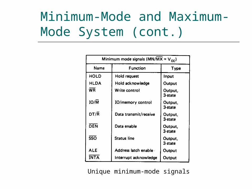
Minimum-Mode Interface (cont)
The minimum-mode signals can be divided into the following basic groups AddressData bus Status signals Control signals Interrupt signals DMA interface signals
Minimum-Mode Interface (cont)
AddressData bus The address bus is used to carry address information to
the memory and IO ports The address bus is 20-bit long and consists of signal lines
A0 through A19
A 20-bit address gives the 8088 a 1 Mbyte memory address space
Only address line A0 through A15 are used when addressing IO
This give an IO address space of 64 Kbytes The 8088 has 8 multiplexed addressdata bus lines
(A0~A7)
8086 has 16 multiplexed addressdata bus lines (A0~A15)
Minimum-Mode Interface (cont)
Status signals The four most significant address A19 through A16
are multiplexed with status signal S6 through S3
Bits S4 and S3 together form a 2-bit binary code that identifies which of the internal segment registers was used to generate the physical address
S5 is the logic level of the internal interrupt flag S6 is always at the 0 logic level
Minimum-Mode Interface (cont)
Minimum-Mode Interface (cont)
Minimum-Mode Interface (cont)
Maximum-Mode Interface
The maximum-mode configuration is mainly used for implementing a multiprocessorcoprocessor system environment Multiple processors exist in the system Each executes its own program
Global resources and local resources The former are common to all processors The latter are assigned to specific processors
In the maximum-mode facilities are provided for implementing allocation of global resources and passing bus control to other microprocessors sharing the system bus
Maximum-Mode Interface (cont)
8088 maximum-mode block diagram
Maximum-Mode Interface (cont)
8086 maximum-mode block diagram
Maximum-Mode Interface (cont)
8288 bus controller
Block diagram and pin layout of 8288
Maximum-Mode Interface (cont)
8288 bus controller In the maximum-mode 80888086 outputs a
status code on three signal line S0 S1 S2 prior to the initialization of each bus cycle
The 3-bit bus status code identifies which type of bus cycle is to follow and are input to the external bus controller device 8288
The 8288 produces one or two command signals for each bus cycle
Maximum-Mode Interface (cont)
8288 bus controller
Bus status code
Maximum-Mode Interface (cont)
Maximum-Mode Interface (cont)
Maximum-Mode Interface (cont)
Queue status signals The 2-bit queue status code QS0 and QS1 tells
the external circuitry what type of information was removed form the queue during the previous clock cycle
Queue status code
Electrical Characteristics
Power is applied between pin 40 (Vcc) and pins 1 (GND) and 20 (GND)
The nominal value of Vcc is specified as +5V dc with a tolerance of plusmn10
Both 8088 and 8086 draw a maximum of 340mA from the supply
IO voltage levels
System Clock
The time base for synchronization of the internal and external operations of the microprocessor in a microcomputer system is provided by the clock (CLK) input signal The standard 8088 operates at 5 MHz and the
8088-2 operates at 8 MHz The 8086 is manufactured in three speeds 5-
MHz 8086 8-MHz 8086-2 and the 10-MHz 8086-1
The CLK is externally generated by the 8284 clock generator and driver IC
System Clock (cont)
Block diagram of the 8284 clock generator
System Clock (cont)
Block diagram of the 8284 clock generator
System Clock (cont)
Connecting the 8284 to the 8088
15- or 24MHzcrystal
Typical value of CL when used with 15MHz crystal is 12pF
The fundamental crystal frequency is divided by 3 within the 8284 to give either a 5- or 8-MHz clock signal
System Clock (cont)
CLK waveform The signal is specified at Metal Oxide
Semiconductor (MOS)-compatible voltage level The period of the 5-MHz 8088 can range from
200 ns to 500 ns and the maximum rise and fall times of its edges equal 10 ns
System Clock (cont)
PCLK and OSC signals The peripheral clock (PCLK) and oscillator clock
(OSC) signals are provided to drive peripheral ICs The clock output at PCLK is half the frequency of
CLK The OSC output is at the crystal frequency which is three times of CLK
System Clock (cont)
The 8284 can also be driven from an external clock source Applied to the EFI (External Frequency Input) Input FC is used for selection
0 crystal between X1 and X2 is used 1 selects EFI
The CSYNC input is used for external synchronization in systems with multiple clocks
System Clock (cont)
EXAMPLE If the CLK input of an 8086 MPU is to be driven by
a 9-MHz signal what speed version of the 8086 must be used and what frequency crystal must be attached to the 8284
Solution The 8086-1 is the version of the 8086 that can be
run at 9-MHz To create the 9-MHz clock a 27-MHz crystal must be used on the 8284
Bus Cycle and Time States
A bus cycle defines the basic operation that a microprocessor performs to communicate with external devices
Examples of bus cycles are the memory read memory write inputoutput read and inputoutput write
The bus cycle of the 8088 and 8086 microprocessors consists of at least four clock periods
If no bus cycles are required the microprocessor performs what are known as idle states
When READY is held at the 0 level wait states are inserted between states T3 and T4 of the bus cycle
Bus Cycle and Time States (cont)
Bus cycle clock periods idle state and wait state
Bus Cycle and Time States (cont)
EXAMPLE What is the duration of the bus cycle in the 8088-
based microcomputer if the clock is 8 MHz and the two wait states are inserted
Solution The duration of the bus cycle in an 8 MHz system
is given by tcyc = 500 ns + N x 125 ns
In this expression the N stands for the number of waits states For a bus cycle with two wait states we get
tcyc = 500 ns + 2 x 125 ns = 500 ns + 250 ns = 750 ns
Hardware Organization of the Memory Address Space
1Mx8 memory bank of the 8088
Hardware Organization of the Memory Address Space (cont)
High and low memory banks of the 8086
Hardware Organization of the Memory Address Space (cont)
Byte transfer by the 8088
Hardware Organization of the Memory Address Space (cont)
Word transfer by the 8088
Hardware Organization of the Memory Address Space (cont)
Even address byte transfer by the 8086
Hardware Organization of the Memory Address Space (cont)
Odd address byte transfer by the 8086
Hardware Organization of the Memory Address Space (cont)
Even address word transfer by the 8086
Hardware Organization of the Memory Address Space (cont)
Odd-address word transfer by the 8086
Hardware Organization of the Memory Address Space (cont)
EXAMPLE Is the word at memory address 0123116 of an
8086-based microcomputer aligned or misaligned How many cycle are required to read it from memory
Solution The first byte of the word is the second byte at
the aligned-word address 0123016 Therefore the word is misaligned and required two bus cycles to be read from memory
Address Bus Status Codes
Whenever a memory bus cycle is in progress an address bus status code S4S3 is output by the processor S4S3 identifies which one of the four segment
register is used to generate the physical address in the current bus cycle 1048729
S4S3=00 identifies the extra segment register (ES)
S4S3=01 identifies the stack segment register (SS)
S4S3=10 identifies the code segment register (CS)
S4S3=11 identifies the data segment register (DS)
The memory address reach of the microprocessor can thus be expanded to 4 Mbytes
Memory Control Signals
Minimum-mode memory control signals
Memory Control Signals (cont)
Minimum-mode memory control signals (8088) ALE ndash Address Latch Enable ndash used to latch
the address in external memory IOM ndash Input-OutputMemory ndash signal external
circuitry whether a memory of IO bus cycle is in progress
DTR ndash Data TransmitReceive ndash signal external circuitry whether the 8088 is transmitting or receiving data over the bus 1048729
RD ndash Read ndash identifies that a read bus cycle is in progress
WR ndash Write ndash identifies that a write bus cycle is in progress
DEN ndash Data Enable ndash used to enable the data bus 1048729
SSO ndash Status Line ndash identifies whether a code or data access is in progress
Memory Control Signals (cont)
The control signals for the 8086rsquos minimum-mode memory interface differs in three ways IOM signal is replaced by MIO signal The signal SSO is removed from the interface BHE (bank high enable) is added to the interface
and is used to select input for the high bank of memory in the 8086rsquos memory subsystem
Memory Control Signals (cont)
Maximum-mode memory control signals
Memory Control Signals (cont)
Maximum-mode memory control signals MRDC ndash Memory Read Command 1048729 MWTC ndash Memory Write Command 1048729 AMWC ndash Advanced Memory Write Command
Read and Write Bus Cycle
Read cycle
Minimum-mode memory read bus cycle of the 8088
Read and Write Bus Cycle (cont)
Read cycle
Minimum-mode memory read bus cycle of the 8086
Read and Write Bus Cycle (cont)
Read cycle
Maximum-mode memory read bus cycle of the 8086
Read and Write Bus Cycle (cont)
Write cycle
Minimum-mode memory write bus cycle of the 8088
Read and Write Bus Cycle (cont)
Write cycle
Maximum-mode memory write bus cycle of the 8086
Memory Interface Circuit
Address bus latches and buffers Bank write and bank read control logic Data bus transceiversbuffers Address decoders
Memory Interface Circuit (cont)
Memory interface block diagram
Memory Interface Circuit (cont)
Address bus latches and buffers
Block diagram of a D-type latch
Memory Interface Circuit (cont)
Address bus latches and buffers
Circuit diagram of the 74F373
Memory Interface Circuit (cont)
A review of flip-floplatch logic
Positive edge-triggered D flip-flop
Memory Interface Circuit (cont)
A review of flip-floplatch logic
Positive edge-triggered JK flip-flop
Memory Interface Circuit (cont)
A review of flip-floplatch logic
D-type latch
Memory Interface Circuit (cont)
Address bus latches and buffers
Address latch circuit
Memory Interface Circuit (cont)
Bank write and bank read control logic
Bank write control logic Bank read control logic
Memory Interface Circuit (cont)
Data bus transceivers
Block diagram and circuit diagram of the 74F245 octal bus transceiver
Memory Interface Circuit (cont)
Data bus transceivers
Data bus transceiver circuit
Memory Interface Circuit (cont)
Address decoder
Address bus configuration with address decoding
Memory Interface Circuit (cont)
Address decoder
Block diagram and operation of the 74F139 decoder
Memory Interface Circuit (cont)
Address decoder
Circuit diagram of the 74F139 decoder
Memory Interface Circuit (cont)
Address decoder
Address decoder circuit using 74F139
Memory Interface Circuit (cont)
Address decoder
Block diagram and operation of the 74F138 decoder
Memory Interface Circuit (cont)
Address decoder
Circuit diagram of the 74F138 decoder
Memory Interface Circuit (cont)
Address decoder
Address decoder circuit using 74F138
Types of InputOutput
The IO system allows peripherals to provide data or receive results of processing the data Using IO ports
The 80888086 MPU can employ two types of IO Isolated IO Memory-mapped IO
They differ in how IO ports are mapped into the address space
Types of InputOutput (cont)
Isolated inputoutput When using isolated IO in a microcomputer
system the IO device are treated separate from memory
The memory address space contains 1 M consecutive byte address in the range 0000016 through FFFFF16
The IO address space contains 64K consecutive byte addresses in the range 000016 through FFFF16
The bytes in two consecutive IO addresses can be accessed as word-wide data
Page 0 000016 00FF16
Certain IO instructions can only perform in this range
Types of InputOutput (cont)
Isolated inputoutput
80888086 memory and IO address spaces
Types of InputOutput (cont)
Isolated inputoutput
Isolated IO ports
Types of InputOutput (cont)
Isolated inputoutput Advantages
The complete 1Mbyte memory address space is available for use with memory
Special instructions have been provided to perform IO operations with maximized performance
The bytes in two consecutive IO addresses can be accessed as word-wide data
Disadvantages All input and output data transfers must take place
between the AL or AX register and IO port
Types of InputOutput (cont)
Memory-mapped inputoutput MPU looks at the IO port as though it is a storage
location in memory Some of the memory address space is dedicated to IO
ports Instructions that affect data in memory are used
instead of the special IO instructions More instructions and addressing modes are available to
perform IO operations IO transfers can take place between IO port and other
internal registers The memory instructions tend to execute slower
than those specifically designed for isolated IO Part of the memory address space is lost
Types of InputOutput(cont)
Memory-mapped inputoutput
Memory mapped IO ports
Isolated InputOutput Interface
IO devices Keyboard Printer Mouse 82C55A etc
Functions of interface circuit Select the IO port Latch output data Sample input data Synchronize data transfer Translate between TTL voltage levels and those
required to operate the IO devices
Isolated InputOutput Interface (cont)
Minimum-mode interface
Minimum-mode 8088 system IO interface
Isolated InputOutput Interface (cont)
Minimum-mode interface
Minimum-mode 8086 system IO interface
Isolated InputOutput Interface (cont)
Maximum-mode interface
Maximum-mode 8088 system IO interface
Isolated InputOutput Interface (cont)
Maximum-mode interface
Maximum-mode 8086 system IO interface
Isolated InputOutput Interface (cont)
Maximum-mode interface
IO bus cycle status codes
InputOutput Data Transfer
Inputoutput data transfers in the 8088 and 8086 microcomputers can be either byte-wide or word-wide
IO addresses are 16 bits in length and are output by the 8088 to the IO interface over bus lines AD0 through AD7 and A8 through A15
In 8088 the word transfers is performed as two consecutive byte-wide data transfer and takes two bus cycle
In 8086 the word transfers can takes either one or two bus cycle
Word-wide IO ports should be aligned at even-address boundaries
InputOutput Data Instructions
InputOutput Data Instructions(cont)
EXAMPLE Write a sequence of instructions that will output
the data FF16 to a byte-wide output port at address AB16 of the IO address space
Solution First the AL register is loaded with FF16 as an
immediate operand in the instruction
MOV AL 0FFH Now the data in AL can be output to the byte-
wide output port with the instruction
OUT 0ABH AL
InputOutput Data Instructions(cont)
EXAMPLE Write a series of instructions that will output FF16 to an
output port located at address B00016 of the IO address space
Solution The DX register must first be loaded with the address
of the output port This is done with the instructionMOV DX 0B000H
Next the data that are to be output must be loaded into AL with the instruction
MOV AL 0FFH Finally the data are output with the instruction
OUT DX AL
InputOutput Data Instructions(cont)
EXAMPLE Data are to be read in from two byte-wide input
ports at addresses AA16 and A916 and then output as a word-wide output port at address B00016 Write a sequence of instructions to perform this inputoutput operation
InputOutput Data Instructions(cont)
Solution First read in the byte at address AA16 into AL and
move it into AHIN AL 0AAHMOV AH AL
Now the other byte can be read into AL by the instructionIN AL 09AH
And to write out the word of dataMOV DX 0B000HOUT DX AX
InputOutput Bus Cycles
Input bus cycle of the 8088
InputOutput Bus Cycles (cont)
Output bus cycle of the 8088
InputOutput Bus Cycles (cont)
Input bus cycle of the 8086
InputOutput Bus Cycles (cont)
Output bus cycle of the 8086
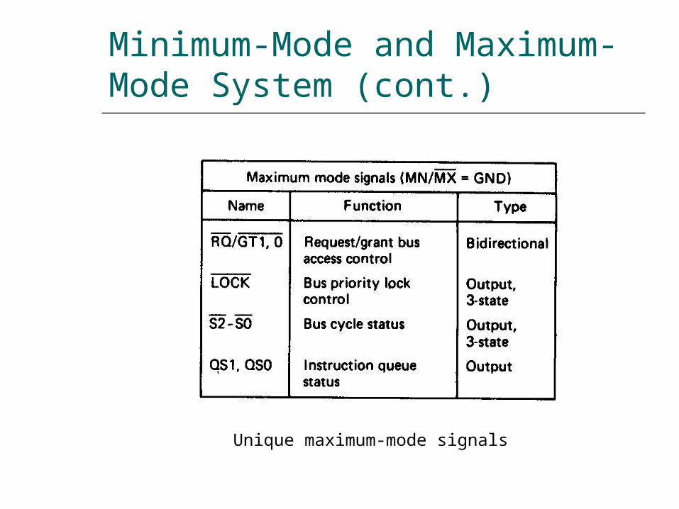
Minimum-Mode Interface (cont)
AddressData bus The address bus is used to carry address information to
the memory and IO ports The address bus is 20-bit long and consists of signal lines
A0 through A19
A 20-bit address gives the 8088 a 1 Mbyte memory address space
Only address line A0 through A15 are used when addressing IO
This give an IO address space of 64 Kbytes The 8088 has 8 multiplexed addressdata bus lines
(A0~A7)
8086 has 16 multiplexed addressdata bus lines (A0~A15)
Minimum-Mode Interface (cont)
Status signals The four most significant address A19 through A16
are multiplexed with status signal S6 through S3
Bits S4 and S3 together form a 2-bit binary code that identifies which of the internal segment registers was used to generate the physical address
S5 is the logic level of the internal interrupt flag S6 is always at the 0 logic level
Minimum-Mode Interface (cont)
Minimum-Mode Interface (cont)
Minimum-Mode Interface (cont)
Maximum-Mode Interface
The maximum-mode configuration is mainly used for implementing a multiprocessorcoprocessor system environment Multiple processors exist in the system Each executes its own program
Global resources and local resources The former are common to all processors The latter are assigned to specific processors
In the maximum-mode facilities are provided for implementing allocation of global resources and passing bus control to other microprocessors sharing the system bus
Maximum-Mode Interface (cont)
8088 maximum-mode block diagram
Maximum-Mode Interface (cont)
8086 maximum-mode block diagram
Maximum-Mode Interface (cont)
8288 bus controller
Block diagram and pin layout of 8288
Maximum-Mode Interface (cont)
8288 bus controller In the maximum-mode 80888086 outputs a
status code on three signal line S0 S1 S2 prior to the initialization of each bus cycle
The 3-bit bus status code identifies which type of bus cycle is to follow and are input to the external bus controller device 8288
The 8288 produces one or two command signals for each bus cycle
Maximum-Mode Interface (cont)
8288 bus controller
Bus status code
Maximum-Mode Interface (cont)
Maximum-Mode Interface (cont)
Maximum-Mode Interface (cont)
Queue status signals The 2-bit queue status code QS0 and QS1 tells
the external circuitry what type of information was removed form the queue during the previous clock cycle
Queue status code
Electrical Characteristics
Power is applied between pin 40 (Vcc) and pins 1 (GND) and 20 (GND)
The nominal value of Vcc is specified as +5V dc with a tolerance of plusmn10
Both 8088 and 8086 draw a maximum of 340mA from the supply
IO voltage levels
System Clock
The time base for synchronization of the internal and external operations of the microprocessor in a microcomputer system is provided by the clock (CLK) input signal The standard 8088 operates at 5 MHz and the
8088-2 operates at 8 MHz The 8086 is manufactured in three speeds 5-
MHz 8086 8-MHz 8086-2 and the 10-MHz 8086-1
The CLK is externally generated by the 8284 clock generator and driver IC
System Clock (cont)
Block diagram of the 8284 clock generator
System Clock (cont)
Block diagram of the 8284 clock generator
System Clock (cont)
Connecting the 8284 to the 8088
15- or 24MHzcrystal
Typical value of CL when used with 15MHz crystal is 12pF
The fundamental crystal frequency is divided by 3 within the 8284 to give either a 5- or 8-MHz clock signal
System Clock (cont)
CLK waveform The signal is specified at Metal Oxide
Semiconductor (MOS)-compatible voltage level The period of the 5-MHz 8088 can range from
200 ns to 500 ns and the maximum rise and fall times of its edges equal 10 ns
System Clock (cont)
PCLK and OSC signals The peripheral clock (PCLK) and oscillator clock
(OSC) signals are provided to drive peripheral ICs The clock output at PCLK is half the frequency of
CLK The OSC output is at the crystal frequency which is three times of CLK
System Clock (cont)
The 8284 can also be driven from an external clock source Applied to the EFI (External Frequency Input) Input FC is used for selection
0 crystal between X1 and X2 is used 1 selects EFI
The CSYNC input is used for external synchronization in systems with multiple clocks
System Clock (cont)
EXAMPLE If the CLK input of an 8086 MPU is to be driven by
a 9-MHz signal what speed version of the 8086 must be used and what frequency crystal must be attached to the 8284
Solution The 8086-1 is the version of the 8086 that can be
run at 9-MHz To create the 9-MHz clock a 27-MHz crystal must be used on the 8284
Bus Cycle and Time States
A bus cycle defines the basic operation that a microprocessor performs to communicate with external devices
Examples of bus cycles are the memory read memory write inputoutput read and inputoutput write
The bus cycle of the 8088 and 8086 microprocessors consists of at least four clock periods
If no bus cycles are required the microprocessor performs what are known as idle states
When READY is held at the 0 level wait states are inserted between states T3 and T4 of the bus cycle
Bus Cycle and Time States (cont)
Bus cycle clock periods idle state and wait state
Bus Cycle and Time States (cont)
EXAMPLE What is the duration of the bus cycle in the 8088-
based microcomputer if the clock is 8 MHz and the two wait states are inserted
Solution The duration of the bus cycle in an 8 MHz system
is given by tcyc = 500 ns + N x 125 ns
In this expression the N stands for the number of waits states For a bus cycle with two wait states we get
tcyc = 500 ns + 2 x 125 ns = 500 ns + 250 ns = 750 ns
Hardware Organization of the Memory Address Space
1Mx8 memory bank of the 8088
Hardware Organization of the Memory Address Space (cont)
High and low memory banks of the 8086
Hardware Organization of the Memory Address Space (cont)
Byte transfer by the 8088
Hardware Organization of the Memory Address Space (cont)
Word transfer by the 8088
Hardware Organization of the Memory Address Space (cont)
Even address byte transfer by the 8086
Hardware Organization of the Memory Address Space (cont)
Odd address byte transfer by the 8086
Hardware Organization of the Memory Address Space (cont)
Even address word transfer by the 8086
Hardware Organization of the Memory Address Space (cont)
Odd-address word transfer by the 8086
Hardware Organization of the Memory Address Space (cont)
EXAMPLE Is the word at memory address 0123116 of an
8086-based microcomputer aligned or misaligned How many cycle are required to read it from memory
Solution The first byte of the word is the second byte at
the aligned-word address 0123016 Therefore the word is misaligned and required two bus cycles to be read from memory
Address Bus Status Codes
Whenever a memory bus cycle is in progress an address bus status code S4S3 is output by the processor S4S3 identifies which one of the four segment
register is used to generate the physical address in the current bus cycle 1048729
S4S3=00 identifies the extra segment register (ES)
S4S3=01 identifies the stack segment register (SS)
S4S3=10 identifies the code segment register (CS)
S4S3=11 identifies the data segment register (DS)
The memory address reach of the microprocessor can thus be expanded to 4 Mbytes
Memory Control Signals
Minimum-mode memory control signals
Memory Control Signals (cont)
Minimum-mode memory control signals (8088) ALE ndash Address Latch Enable ndash used to latch
the address in external memory IOM ndash Input-OutputMemory ndash signal external
circuitry whether a memory of IO bus cycle is in progress
DTR ndash Data TransmitReceive ndash signal external circuitry whether the 8088 is transmitting or receiving data over the bus 1048729
RD ndash Read ndash identifies that a read bus cycle is in progress
WR ndash Write ndash identifies that a write bus cycle is in progress
DEN ndash Data Enable ndash used to enable the data bus 1048729
SSO ndash Status Line ndash identifies whether a code or data access is in progress
Memory Control Signals (cont)
The control signals for the 8086rsquos minimum-mode memory interface differs in three ways IOM signal is replaced by MIO signal The signal SSO is removed from the interface BHE (bank high enable) is added to the interface
and is used to select input for the high bank of memory in the 8086rsquos memory subsystem
Memory Control Signals (cont)
Maximum-mode memory control signals
Memory Control Signals (cont)
Maximum-mode memory control signals MRDC ndash Memory Read Command 1048729 MWTC ndash Memory Write Command 1048729 AMWC ndash Advanced Memory Write Command
Read and Write Bus Cycle
Read cycle
Minimum-mode memory read bus cycle of the 8088
Read and Write Bus Cycle (cont)
Read cycle
Minimum-mode memory read bus cycle of the 8086
Read and Write Bus Cycle (cont)
Read cycle
Maximum-mode memory read bus cycle of the 8086
Read and Write Bus Cycle (cont)
Write cycle
Minimum-mode memory write bus cycle of the 8088
Read and Write Bus Cycle (cont)
Write cycle
Maximum-mode memory write bus cycle of the 8086
Memory Interface Circuit
Address bus latches and buffers Bank write and bank read control logic Data bus transceiversbuffers Address decoders
Memory Interface Circuit (cont)
Memory interface block diagram
Memory Interface Circuit (cont)
Address bus latches and buffers
Block diagram of a D-type latch
Memory Interface Circuit (cont)
Address bus latches and buffers
Circuit diagram of the 74F373
Memory Interface Circuit (cont)
A review of flip-floplatch logic
Positive edge-triggered D flip-flop
Memory Interface Circuit (cont)
A review of flip-floplatch logic
Positive edge-triggered JK flip-flop
Memory Interface Circuit (cont)
A review of flip-floplatch logic
D-type latch
Memory Interface Circuit (cont)
Address bus latches and buffers
Address latch circuit
Memory Interface Circuit (cont)
Bank write and bank read control logic
Bank write control logic Bank read control logic
Memory Interface Circuit (cont)
Data bus transceivers
Block diagram and circuit diagram of the 74F245 octal bus transceiver
Memory Interface Circuit (cont)
Data bus transceivers
Data bus transceiver circuit
Memory Interface Circuit (cont)
Address decoder
Address bus configuration with address decoding
Memory Interface Circuit (cont)
Address decoder
Block diagram and operation of the 74F139 decoder
Memory Interface Circuit (cont)
Address decoder
Circuit diagram of the 74F139 decoder
Memory Interface Circuit (cont)
Address decoder
Address decoder circuit using 74F139
Memory Interface Circuit (cont)
Address decoder
Block diagram and operation of the 74F138 decoder
Memory Interface Circuit (cont)
Address decoder
Circuit diagram of the 74F138 decoder
Memory Interface Circuit (cont)
Address decoder
Address decoder circuit using 74F138
Types of InputOutput
The IO system allows peripherals to provide data or receive results of processing the data Using IO ports
The 80888086 MPU can employ two types of IO Isolated IO Memory-mapped IO
They differ in how IO ports are mapped into the address space
Types of InputOutput (cont)
Isolated inputoutput When using isolated IO in a microcomputer
system the IO device are treated separate from memory
The memory address space contains 1 M consecutive byte address in the range 0000016 through FFFFF16
The IO address space contains 64K consecutive byte addresses in the range 000016 through FFFF16
The bytes in two consecutive IO addresses can be accessed as word-wide data
Page 0 000016 00FF16
Certain IO instructions can only perform in this range
Types of InputOutput (cont)
Isolated inputoutput
80888086 memory and IO address spaces
Types of InputOutput (cont)
Isolated inputoutput
Isolated IO ports
Types of InputOutput (cont)
Isolated inputoutput Advantages
The complete 1Mbyte memory address space is available for use with memory
Special instructions have been provided to perform IO operations with maximized performance
The bytes in two consecutive IO addresses can be accessed as word-wide data
Disadvantages All input and output data transfers must take place
between the AL or AX register and IO port
Types of InputOutput (cont)
Memory-mapped inputoutput MPU looks at the IO port as though it is a storage
location in memory Some of the memory address space is dedicated to IO
ports Instructions that affect data in memory are used
instead of the special IO instructions More instructions and addressing modes are available to
perform IO operations IO transfers can take place between IO port and other
internal registers The memory instructions tend to execute slower
than those specifically designed for isolated IO Part of the memory address space is lost
Types of InputOutput(cont)
Memory-mapped inputoutput
Memory mapped IO ports
Isolated InputOutput Interface
IO devices Keyboard Printer Mouse 82C55A etc
Functions of interface circuit Select the IO port Latch output data Sample input data Synchronize data transfer Translate between TTL voltage levels and those
required to operate the IO devices
Isolated InputOutput Interface (cont)
Minimum-mode interface
Minimum-mode 8088 system IO interface
Isolated InputOutput Interface (cont)
Minimum-mode interface
Minimum-mode 8086 system IO interface
Isolated InputOutput Interface (cont)
Maximum-mode interface
Maximum-mode 8088 system IO interface
Isolated InputOutput Interface (cont)
Maximum-mode interface
Maximum-mode 8086 system IO interface
Isolated InputOutput Interface (cont)
Maximum-mode interface
IO bus cycle status codes
InputOutput Data Transfer
Inputoutput data transfers in the 8088 and 8086 microcomputers can be either byte-wide or word-wide
IO addresses are 16 bits in length and are output by the 8088 to the IO interface over bus lines AD0 through AD7 and A8 through A15
In 8088 the word transfers is performed as two consecutive byte-wide data transfer and takes two bus cycle
In 8086 the word transfers can takes either one or two bus cycle
Word-wide IO ports should be aligned at even-address boundaries
InputOutput Data Instructions
InputOutput Data Instructions(cont)
EXAMPLE Write a sequence of instructions that will output
the data FF16 to a byte-wide output port at address AB16 of the IO address space
Solution First the AL register is loaded with FF16 as an
immediate operand in the instruction
MOV AL 0FFH Now the data in AL can be output to the byte-
wide output port with the instruction
OUT 0ABH AL
InputOutput Data Instructions(cont)
EXAMPLE Write a series of instructions that will output FF16 to an
output port located at address B00016 of the IO address space
Solution The DX register must first be loaded with the address
of the output port This is done with the instructionMOV DX 0B000H
Next the data that are to be output must be loaded into AL with the instruction
MOV AL 0FFH Finally the data are output with the instruction
OUT DX AL
InputOutput Data Instructions(cont)
EXAMPLE Data are to be read in from two byte-wide input
ports at addresses AA16 and A916 and then output as a word-wide output port at address B00016 Write a sequence of instructions to perform this inputoutput operation
InputOutput Data Instructions(cont)
Solution First read in the byte at address AA16 into AL and
move it into AHIN AL 0AAHMOV AH AL
Now the other byte can be read into AL by the instructionIN AL 09AH
And to write out the word of dataMOV DX 0B000HOUT DX AX
InputOutput Bus Cycles
Input bus cycle of the 8088
InputOutput Bus Cycles (cont)
Output bus cycle of the 8088
InputOutput Bus Cycles (cont)
Input bus cycle of the 8086
InputOutput Bus Cycles (cont)
Output bus cycle of the 8086
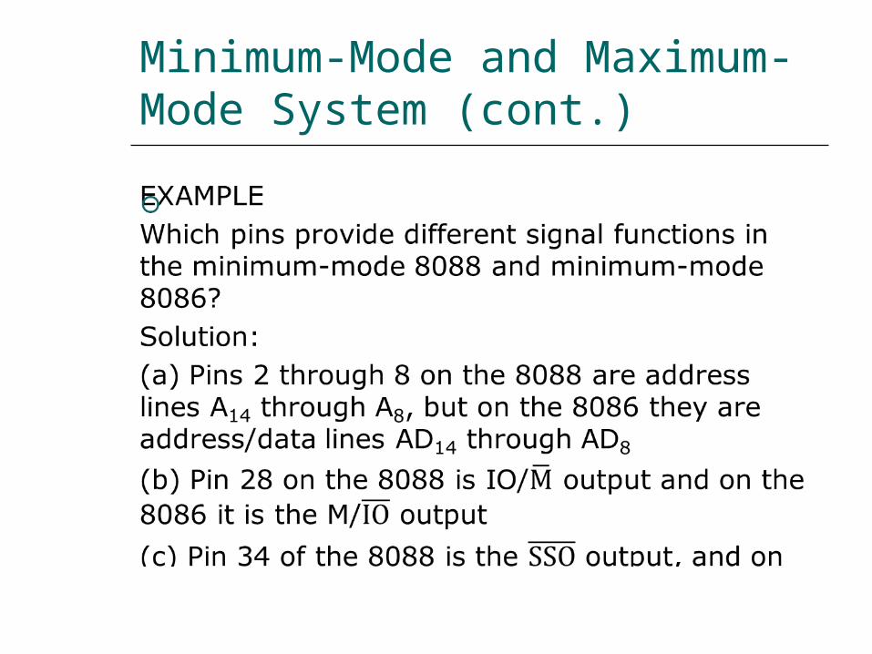
Minimum-Mode Interface (cont)
Status signals The four most significant address A19 through A16
are multiplexed with status signal S6 through S3
Bits S4 and S3 together form a 2-bit binary code that identifies which of the internal segment registers was used to generate the physical address
S5 is the logic level of the internal interrupt flag S6 is always at the 0 logic level
Minimum-Mode Interface (cont)
Minimum-Mode Interface (cont)
Minimum-Mode Interface (cont)
Maximum-Mode Interface
The maximum-mode configuration is mainly used for implementing a multiprocessorcoprocessor system environment Multiple processors exist in the system Each executes its own program
Global resources and local resources The former are common to all processors The latter are assigned to specific processors
In the maximum-mode facilities are provided for implementing allocation of global resources and passing bus control to other microprocessors sharing the system bus
Maximum-Mode Interface (cont)
8088 maximum-mode block diagram
Maximum-Mode Interface (cont)
8086 maximum-mode block diagram
Maximum-Mode Interface (cont)
8288 bus controller
Block diagram and pin layout of 8288
Maximum-Mode Interface (cont)
8288 bus controller In the maximum-mode 80888086 outputs a
status code on three signal line S0 S1 S2 prior to the initialization of each bus cycle
The 3-bit bus status code identifies which type of bus cycle is to follow and are input to the external bus controller device 8288
The 8288 produces one or two command signals for each bus cycle
Maximum-Mode Interface (cont)
8288 bus controller
Bus status code
Maximum-Mode Interface (cont)
Maximum-Mode Interface (cont)
Maximum-Mode Interface (cont)
Queue status signals The 2-bit queue status code QS0 and QS1 tells
the external circuitry what type of information was removed form the queue during the previous clock cycle
Queue status code
Electrical Characteristics
Power is applied between pin 40 (Vcc) and pins 1 (GND) and 20 (GND)
The nominal value of Vcc is specified as +5V dc with a tolerance of plusmn10
Both 8088 and 8086 draw a maximum of 340mA from the supply
IO voltage levels
System Clock
The time base for synchronization of the internal and external operations of the microprocessor in a microcomputer system is provided by the clock (CLK) input signal The standard 8088 operates at 5 MHz and the
8088-2 operates at 8 MHz The 8086 is manufactured in three speeds 5-
MHz 8086 8-MHz 8086-2 and the 10-MHz 8086-1
The CLK is externally generated by the 8284 clock generator and driver IC
System Clock (cont)
Block diagram of the 8284 clock generator
System Clock (cont)
Block diagram of the 8284 clock generator
System Clock (cont)
Connecting the 8284 to the 8088
15- or 24MHzcrystal
Typical value of CL when used with 15MHz crystal is 12pF
The fundamental crystal frequency is divided by 3 within the 8284 to give either a 5- or 8-MHz clock signal
System Clock (cont)
CLK waveform The signal is specified at Metal Oxide
Semiconductor (MOS)-compatible voltage level The period of the 5-MHz 8088 can range from
200 ns to 500 ns and the maximum rise and fall times of its edges equal 10 ns
System Clock (cont)
PCLK and OSC signals The peripheral clock (PCLK) and oscillator clock
(OSC) signals are provided to drive peripheral ICs The clock output at PCLK is half the frequency of
CLK The OSC output is at the crystal frequency which is three times of CLK
System Clock (cont)
The 8284 can also be driven from an external clock source Applied to the EFI (External Frequency Input) Input FC is used for selection
0 crystal between X1 and X2 is used 1 selects EFI
The CSYNC input is used for external synchronization in systems with multiple clocks
System Clock (cont)
EXAMPLE If the CLK input of an 8086 MPU is to be driven by
a 9-MHz signal what speed version of the 8086 must be used and what frequency crystal must be attached to the 8284
Solution The 8086-1 is the version of the 8086 that can be
run at 9-MHz To create the 9-MHz clock a 27-MHz crystal must be used on the 8284
Bus Cycle and Time States
A bus cycle defines the basic operation that a microprocessor performs to communicate with external devices
Examples of bus cycles are the memory read memory write inputoutput read and inputoutput write
The bus cycle of the 8088 and 8086 microprocessors consists of at least four clock periods
If no bus cycles are required the microprocessor performs what are known as idle states
When READY is held at the 0 level wait states are inserted between states T3 and T4 of the bus cycle
Bus Cycle and Time States (cont)
Bus cycle clock periods idle state and wait state
Bus Cycle and Time States (cont)
EXAMPLE What is the duration of the bus cycle in the 8088-
based microcomputer if the clock is 8 MHz and the two wait states are inserted
Solution The duration of the bus cycle in an 8 MHz system
is given by tcyc = 500 ns + N x 125 ns
In this expression the N stands for the number of waits states For a bus cycle with two wait states we get
tcyc = 500 ns + 2 x 125 ns = 500 ns + 250 ns = 750 ns
Hardware Organization of the Memory Address Space
1Mx8 memory bank of the 8088
Hardware Organization of the Memory Address Space (cont)
High and low memory banks of the 8086
Hardware Organization of the Memory Address Space (cont)
Byte transfer by the 8088
Hardware Organization of the Memory Address Space (cont)
Word transfer by the 8088
Hardware Organization of the Memory Address Space (cont)
Even address byte transfer by the 8086
Hardware Organization of the Memory Address Space (cont)
Odd address byte transfer by the 8086
Hardware Organization of the Memory Address Space (cont)
Even address word transfer by the 8086
Hardware Organization of the Memory Address Space (cont)
Odd-address word transfer by the 8086
Hardware Organization of the Memory Address Space (cont)
EXAMPLE Is the word at memory address 0123116 of an
8086-based microcomputer aligned or misaligned How many cycle are required to read it from memory
Solution The first byte of the word is the second byte at
the aligned-word address 0123016 Therefore the word is misaligned and required two bus cycles to be read from memory
Address Bus Status Codes
Whenever a memory bus cycle is in progress an address bus status code S4S3 is output by the processor S4S3 identifies which one of the four segment
register is used to generate the physical address in the current bus cycle 1048729
S4S3=00 identifies the extra segment register (ES)
S4S3=01 identifies the stack segment register (SS)
S4S3=10 identifies the code segment register (CS)
S4S3=11 identifies the data segment register (DS)
The memory address reach of the microprocessor can thus be expanded to 4 Mbytes
Memory Control Signals
Minimum-mode memory control signals
Memory Control Signals (cont)
Minimum-mode memory control signals (8088) ALE ndash Address Latch Enable ndash used to latch
the address in external memory IOM ndash Input-OutputMemory ndash signal external
circuitry whether a memory of IO bus cycle is in progress
DTR ndash Data TransmitReceive ndash signal external circuitry whether the 8088 is transmitting or receiving data over the bus 1048729
RD ndash Read ndash identifies that a read bus cycle is in progress
WR ndash Write ndash identifies that a write bus cycle is in progress
DEN ndash Data Enable ndash used to enable the data bus 1048729
SSO ndash Status Line ndash identifies whether a code or data access is in progress
Memory Control Signals (cont)
The control signals for the 8086rsquos minimum-mode memory interface differs in three ways IOM signal is replaced by MIO signal The signal SSO is removed from the interface BHE (bank high enable) is added to the interface
and is used to select input for the high bank of memory in the 8086rsquos memory subsystem
Memory Control Signals (cont)
Maximum-mode memory control signals
Memory Control Signals (cont)
Maximum-mode memory control signals MRDC ndash Memory Read Command 1048729 MWTC ndash Memory Write Command 1048729 AMWC ndash Advanced Memory Write Command
Read and Write Bus Cycle
Read cycle
Minimum-mode memory read bus cycle of the 8088
Read and Write Bus Cycle (cont)
Read cycle
Minimum-mode memory read bus cycle of the 8086
Read and Write Bus Cycle (cont)
Read cycle
Maximum-mode memory read bus cycle of the 8086
Read and Write Bus Cycle (cont)
Write cycle
Minimum-mode memory write bus cycle of the 8088
Read and Write Bus Cycle (cont)
Write cycle
Maximum-mode memory write bus cycle of the 8086
Memory Interface Circuit
Address bus latches and buffers Bank write and bank read control logic Data bus transceiversbuffers Address decoders
Memory Interface Circuit (cont)
Memory interface block diagram
Memory Interface Circuit (cont)
Address bus latches and buffers
Block diagram of a D-type latch
Memory Interface Circuit (cont)
Address bus latches and buffers
Circuit diagram of the 74F373
Memory Interface Circuit (cont)
A review of flip-floplatch logic
Positive edge-triggered D flip-flop
Memory Interface Circuit (cont)
A review of flip-floplatch logic
Positive edge-triggered JK flip-flop
Memory Interface Circuit (cont)
A review of flip-floplatch logic
D-type latch
Memory Interface Circuit (cont)
Address bus latches and buffers
Address latch circuit
Memory Interface Circuit (cont)
Bank write and bank read control logic
Bank write control logic Bank read control logic
Memory Interface Circuit (cont)
Data bus transceivers
Block diagram and circuit diagram of the 74F245 octal bus transceiver
Memory Interface Circuit (cont)
Data bus transceivers
Data bus transceiver circuit
Memory Interface Circuit (cont)
Address decoder
Address bus configuration with address decoding
Memory Interface Circuit (cont)
Address decoder
Block diagram and operation of the 74F139 decoder
Memory Interface Circuit (cont)
Address decoder
Circuit diagram of the 74F139 decoder
Memory Interface Circuit (cont)
Address decoder
Address decoder circuit using 74F139
Memory Interface Circuit (cont)
Address decoder
Block diagram and operation of the 74F138 decoder
Memory Interface Circuit (cont)
Address decoder
Circuit diagram of the 74F138 decoder
Memory Interface Circuit (cont)
Address decoder
Address decoder circuit using 74F138
Types of InputOutput
The IO system allows peripherals to provide data or receive results of processing the data Using IO ports
The 80888086 MPU can employ two types of IO Isolated IO Memory-mapped IO
They differ in how IO ports are mapped into the address space
Types of InputOutput (cont)
Isolated inputoutput When using isolated IO in a microcomputer
system the IO device are treated separate from memory
The memory address space contains 1 M consecutive byte address in the range 0000016 through FFFFF16
The IO address space contains 64K consecutive byte addresses in the range 000016 through FFFF16
The bytes in two consecutive IO addresses can be accessed as word-wide data
Page 0 000016 00FF16
Certain IO instructions can only perform in this range
Types of InputOutput (cont)
Isolated inputoutput
80888086 memory and IO address spaces
Types of InputOutput (cont)
Isolated inputoutput
Isolated IO ports
Types of InputOutput (cont)
Isolated inputoutput Advantages
The complete 1Mbyte memory address space is available for use with memory
Special instructions have been provided to perform IO operations with maximized performance
The bytes in two consecutive IO addresses can be accessed as word-wide data
Disadvantages All input and output data transfers must take place
between the AL or AX register and IO port
Types of InputOutput (cont)
Memory-mapped inputoutput MPU looks at the IO port as though it is a storage
location in memory Some of the memory address space is dedicated to IO
ports Instructions that affect data in memory are used
instead of the special IO instructions More instructions and addressing modes are available to
perform IO operations IO transfers can take place between IO port and other
internal registers The memory instructions tend to execute slower
than those specifically designed for isolated IO Part of the memory address space is lost
Types of InputOutput(cont)
Memory-mapped inputoutput
Memory mapped IO ports
Isolated InputOutput Interface
IO devices Keyboard Printer Mouse 82C55A etc
Functions of interface circuit Select the IO port Latch output data Sample input data Synchronize data transfer Translate between TTL voltage levels and those
required to operate the IO devices
Isolated InputOutput Interface (cont)
Minimum-mode interface
Minimum-mode 8088 system IO interface
Isolated InputOutput Interface (cont)
Minimum-mode interface
Minimum-mode 8086 system IO interface
Isolated InputOutput Interface (cont)
Maximum-mode interface
Maximum-mode 8088 system IO interface
Isolated InputOutput Interface (cont)
Maximum-mode interface
Maximum-mode 8086 system IO interface
Isolated InputOutput Interface (cont)
Maximum-mode interface
IO bus cycle status codes
InputOutput Data Transfer
Inputoutput data transfers in the 8088 and 8086 microcomputers can be either byte-wide or word-wide
IO addresses are 16 bits in length and are output by the 8088 to the IO interface over bus lines AD0 through AD7 and A8 through A15
In 8088 the word transfers is performed as two consecutive byte-wide data transfer and takes two bus cycle
In 8086 the word transfers can takes either one or two bus cycle
Word-wide IO ports should be aligned at even-address boundaries
InputOutput Data Instructions
InputOutput Data Instructions(cont)
EXAMPLE Write a sequence of instructions that will output
the data FF16 to a byte-wide output port at address AB16 of the IO address space
Solution First the AL register is loaded with FF16 as an
immediate operand in the instruction
MOV AL 0FFH Now the data in AL can be output to the byte-
wide output port with the instruction
OUT 0ABH AL
InputOutput Data Instructions(cont)
EXAMPLE Write a series of instructions that will output FF16 to an
output port located at address B00016 of the IO address space
Solution The DX register must first be loaded with the address
of the output port This is done with the instructionMOV DX 0B000H
Next the data that are to be output must be loaded into AL with the instruction
MOV AL 0FFH Finally the data are output with the instruction
OUT DX AL
InputOutput Data Instructions(cont)
EXAMPLE Data are to be read in from two byte-wide input
ports at addresses AA16 and A916 and then output as a word-wide output port at address B00016 Write a sequence of instructions to perform this inputoutput operation
InputOutput Data Instructions(cont)
Solution First read in the byte at address AA16 into AL and
move it into AHIN AL 0AAHMOV AH AL
Now the other byte can be read into AL by the instructionIN AL 09AH
And to write out the word of dataMOV DX 0B000HOUT DX AX
InputOutput Bus Cycles
Input bus cycle of the 8088
InputOutput Bus Cycles (cont)
Output bus cycle of the 8088
InputOutput Bus Cycles (cont)
Input bus cycle of the 8086
InputOutput Bus Cycles (cont)
Output bus cycle of the 8086
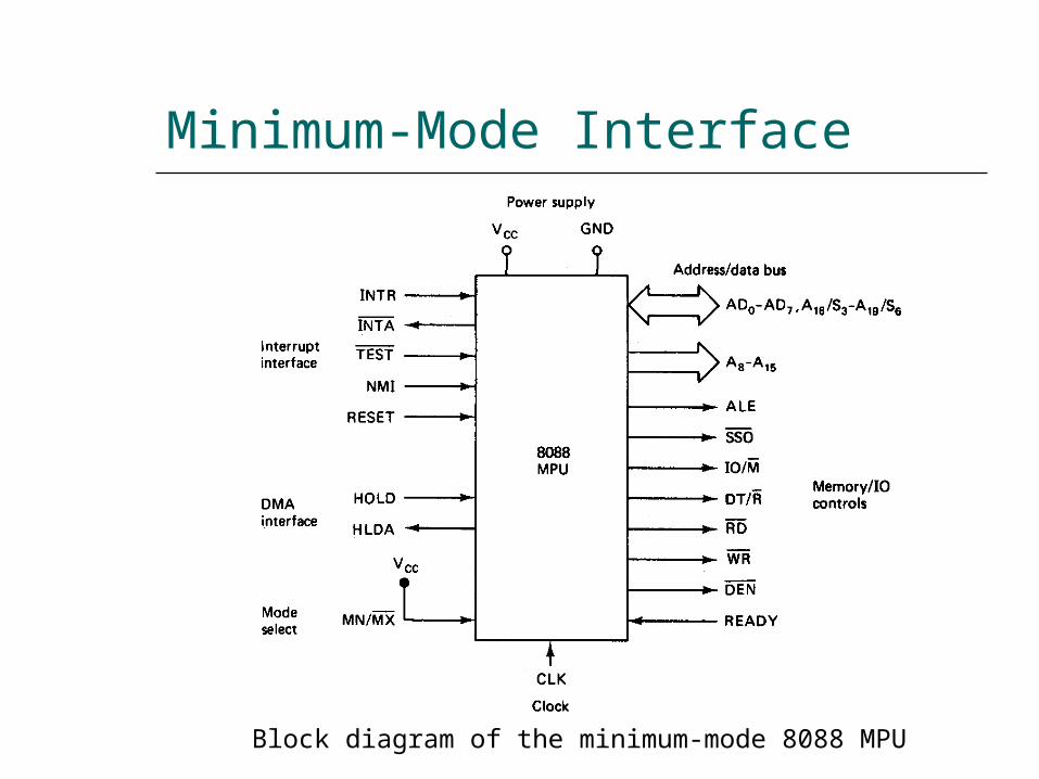
Minimum-Mode Interface (cont)
Minimum-Mode Interface (cont)
Minimum-Mode Interface (cont)
Maximum-Mode Interface
The maximum-mode configuration is mainly used for implementing a multiprocessorcoprocessor system environment Multiple processors exist in the system Each executes its own program
Global resources and local resources The former are common to all processors The latter are assigned to specific processors
In the maximum-mode facilities are provided for implementing allocation of global resources and passing bus control to other microprocessors sharing the system bus
Maximum-Mode Interface (cont)
8088 maximum-mode block diagram
Maximum-Mode Interface (cont)
8086 maximum-mode block diagram
Maximum-Mode Interface (cont)
8288 bus controller
Block diagram and pin layout of 8288
Maximum-Mode Interface (cont)
8288 bus controller In the maximum-mode 80888086 outputs a
status code on three signal line S0 S1 S2 prior to the initialization of each bus cycle
The 3-bit bus status code identifies which type of bus cycle is to follow and are input to the external bus controller device 8288
The 8288 produces one or two command signals for each bus cycle
Maximum-Mode Interface (cont)
8288 bus controller
Bus status code
Maximum-Mode Interface (cont)
Maximum-Mode Interface (cont)
Maximum-Mode Interface (cont)
Queue status signals The 2-bit queue status code QS0 and QS1 tells
the external circuitry what type of information was removed form the queue during the previous clock cycle
Queue status code
Electrical Characteristics
Power is applied between pin 40 (Vcc) and pins 1 (GND) and 20 (GND)
The nominal value of Vcc is specified as +5V dc with a tolerance of plusmn10
Both 8088 and 8086 draw a maximum of 340mA from the supply
IO voltage levels
System Clock
The time base for synchronization of the internal and external operations of the microprocessor in a microcomputer system is provided by the clock (CLK) input signal The standard 8088 operates at 5 MHz and the
8088-2 operates at 8 MHz The 8086 is manufactured in three speeds 5-
MHz 8086 8-MHz 8086-2 and the 10-MHz 8086-1
The CLK is externally generated by the 8284 clock generator and driver IC
System Clock (cont)
Block diagram of the 8284 clock generator
System Clock (cont)
Block diagram of the 8284 clock generator
System Clock (cont)
Connecting the 8284 to the 8088
15- or 24MHzcrystal
Typical value of CL when used with 15MHz crystal is 12pF
The fundamental crystal frequency is divided by 3 within the 8284 to give either a 5- or 8-MHz clock signal
System Clock (cont)
CLK waveform The signal is specified at Metal Oxide
Semiconductor (MOS)-compatible voltage level The period of the 5-MHz 8088 can range from
200 ns to 500 ns and the maximum rise and fall times of its edges equal 10 ns
System Clock (cont)
PCLK and OSC signals The peripheral clock (PCLK) and oscillator clock
(OSC) signals are provided to drive peripheral ICs The clock output at PCLK is half the frequency of
CLK The OSC output is at the crystal frequency which is three times of CLK
System Clock (cont)
The 8284 can also be driven from an external clock source Applied to the EFI (External Frequency Input) Input FC is used for selection
0 crystal between X1 and X2 is used 1 selects EFI
The CSYNC input is used for external synchronization in systems with multiple clocks
System Clock (cont)
EXAMPLE If the CLK input of an 8086 MPU is to be driven by
a 9-MHz signal what speed version of the 8086 must be used and what frequency crystal must be attached to the 8284
Solution The 8086-1 is the version of the 8086 that can be
run at 9-MHz To create the 9-MHz clock a 27-MHz crystal must be used on the 8284
Bus Cycle and Time States
A bus cycle defines the basic operation that a microprocessor performs to communicate with external devices
Examples of bus cycles are the memory read memory write inputoutput read and inputoutput write
The bus cycle of the 8088 and 8086 microprocessors consists of at least four clock periods
If no bus cycles are required the microprocessor performs what are known as idle states
When READY is held at the 0 level wait states are inserted between states T3 and T4 of the bus cycle
Bus Cycle and Time States (cont)
Bus cycle clock periods idle state and wait state
Bus Cycle and Time States (cont)
EXAMPLE What is the duration of the bus cycle in the 8088-
based microcomputer if the clock is 8 MHz and the two wait states are inserted
Solution The duration of the bus cycle in an 8 MHz system
is given by tcyc = 500 ns + N x 125 ns
In this expression the N stands for the number of waits states For a bus cycle with two wait states we get
tcyc = 500 ns + 2 x 125 ns = 500 ns + 250 ns = 750 ns
Hardware Organization of the Memory Address Space
1Mx8 memory bank of the 8088
Hardware Organization of the Memory Address Space (cont)
High and low memory banks of the 8086
Hardware Organization of the Memory Address Space (cont)
Byte transfer by the 8088
Hardware Organization of the Memory Address Space (cont)
Word transfer by the 8088
Hardware Organization of the Memory Address Space (cont)
Even address byte transfer by the 8086
Hardware Organization of the Memory Address Space (cont)
Odd address byte transfer by the 8086
Hardware Organization of the Memory Address Space (cont)
Even address word transfer by the 8086
Hardware Organization of the Memory Address Space (cont)
Odd-address word transfer by the 8086
Hardware Organization of the Memory Address Space (cont)
EXAMPLE Is the word at memory address 0123116 of an
8086-based microcomputer aligned or misaligned How many cycle are required to read it from memory
Solution The first byte of the word is the second byte at
the aligned-word address 0123016 Therefore the word is misaligned and required two bus cycles to be read from memory
Address Bus Status Codes
Whenever a memory bus cycle is in progress an address bus status code S4S3 is output by the processor S4S3 identifies which one of the four segment
register is used to generate the physical address in the current bus cycle 1048729
S4S3=00 identifies the extra segment register (ES)
S4S3=01 identifies the stack segment register (SS)
S4S3=10 identifies the code segment register (CS)
S4S3=11 identifies the data segment register (DS)
The memory address reach of the microprocessor can thus be expanded to 4 Mbytes
Memory Control Signals
Minimum-mode memory control signals
Memory Control Signals (cont)
Minimum-mode memory control signals (8088) ALE ndash Address Latch Enable ndash used to latch
the address in external memory IOM ndash Input-OutputMemory ndash signal external
circuitry whether a memory of IO bus cycle is in progress
DTR ndash Data TransmitReceive ndash signal external circuitry whether the 8088 is transmitting or receiving data over the bus 1048729
RD ndash Read ndash identifies that a read bus cycle is in progress
WR ndash Write ndash identifies that a write bus cycle is in progress
DEN ndash Data Enable ndash used to enable the data bus 1048729
SSO ndash Status Line ndash identifies whether a code or data access is in progress
Memory Control Signals (cont)
The control signals for the 8086rsquos minimum-mode memory interface differs in three ways IOM signal is replaced by MIO signal The signal SSO is removed from the interface BHE (bank high enable) is added to the interface
and is used to select input for the high bank of memory in the 8086rsquos memory subsystem
Memory Control Signals (cont)
Maximum-mode memory control signals
Memory Control Signals (cont)
Maximum-mode memory control signals MRDC ndash Memory Read Command 1048729 MWTC ndash Memory Write Command 1048729 AMWC ndash Advanced Memory Write Command
Read and Write Bus Cycle
Read cycle
Minimum-mode memory read bus cycle of the 8088
Read and Write Bus Cycle (cont)
Read cycle
Minimum-mode memory read bus cycle of the 8086
Read and Write Bus Cycle (cont)
Read cycle
Maximum-mode memory read bus cycle of the 8086
Read and Write Bus Cycle (cont)
Write cycle
Minimum-mode memory write bus cycle of the 8088
Read and Write Bus Cycle (cont)
Write cycle
Maximum-mode memory write bus cycle of the 8086
Memory Interface Circuit
Address bus latches and buffers Bank write and bank read control logic Data bus transceiversbuffers Address decoders
Memory Interface Circuit (cont)
Memory interface block diagram
Memory Interface Circuit (cont)
Address bus latches and buffers
Block diagram of a D-type latch
Memory Interface Circuit (cont)
Address bus latches and buffers
Circuit diagram of the 74F373
Memory Interface Circuit (cont)
A review of flip-floplatch logic
Positive edge-triggered D flip-flop
Memory Interface Circuit (cont)
A review of flip-floplatch logic
Positive edge-triggered JK flip-flop
Memory Interface Circuit (cont)
A review of flip-floplatch logic
D-type latch
Memory Interface Circuit (cont)
Address bus latches and buffers
Address latch circuit
Memory Interface Circuit (cont)
Bank write and bank read control logic
Bank write control logic Bank read control logic
Memory Interface Circuit (cont)
Data bus transceivers
Block diagram and circuit diagram of the 74F245 octal bus transceiver
Memory Interface Circuit (cont)
Data bus transceivers
Data bus transceiver circuit
Memory Interface Circuit (cont)
Address decoder
Address bus configuration with address decoding
Memory Interface Circuit (cont)
Address decoder
Block diagram and operation of the 74F139 decoder
Memory Interface Circuit (cont)
Address decoder
Circuit diagram of the 74F139 decoder
Memory Interface Circuit (cont)
Address decoder
Address decoder circuit using 74F139
Memory Interface Circuit (cont)
Address decoder
Block diagram and operation of the 74F138 decoder
Memory Interface Circuit (cont)
Address decoder
Circuit diagram of the 74F138 decoder
Memory Interface Circuit (cont)
Address decoder
Address decoder circuit using 74F138
Types of InputOutput
The IO system allows peripherals to provide data or receive results of processing the data Using IO ports
The 80888086 MPU can employ two types of IO Isolated IO Memory-mapped IO
They differ in how IO ports are mapped into the address space
Types of InputOutput (cont)
Isolated inputoutput When using isolated IO in a microcomputer
system the IO device are treated separate from memory
The memory address space contains 1 M consecutive byte address in the range 0000016 through FFFFF16
The IO address space contains 64K consecutive byte addresses in the range 000016 through FFFF16
The bytes in two consecutive IO addresses can be accessed as word-wide data
Page 0 000016 00FF16
Certain IO instructions can only perform in this range
Types of InputOutput (cont)
Isolated inputoutput
80888086 memory and IO address spaces
Types of InputOutput (cont)
Isolated inputoutput
Isolated IO ports
Types of InputOutput (cont)
Isolated inputoutput Advantages
The complete 1Mbyte memory address space is available for use with memory
Special instructions have been provided to perform IO operations with maximized performance
The bytes in two consecutive IO addresses can be accessed as word-wide data
Disadvantages All input and output data transfers must take place
between the AL or AX register and IO port
Types of InputOutput (cont)
Memory-mapped inputoutput MPU looks at the IO port as though it is a storage
location in memory Some of the memory address space is dedicated to IO
ports Instructions that affect data in memory are used
instead of the special IO instructions More instructions and addressing modes are available to
perform IO operations IO transfers can take place between IO port and other
internal registers The memory instructions tend to execute slower
than those specifically designed for isolated IO Part of the memory address space is lost
Types of InputOutput(cont)
Memory-mapped inputoutput
Memory mapped IO ports
Isolated InputOutput Interface
IO devices Keyboard Printer Mouse 82C55A etc
Functions of interface circuit Select the IO port Latch output data Sample input data Synchronize data transfer Translate between TTL voltage levels and those
required to operate the IO devices
Isolated InputOutput Interface (cont)
Minimum-mode interface
Minimum-mode 8088 system IO interface
Isolated InputOutput Interface (cont)
Minimum-mode interface
Minimum-mode 8086 system IO interface
Isolated InputOutput Interface (cont)
Maximum-mode interface
Maximum-mode 8088 system IO interface
Isolated InputOutput Interface (cont)
Maximum-mode interface
Maximum-mode 8086 system IO interface
Isolated InputOutput Interface (cont)
Maximum-mode interface
IO bus cycle status codes
InputOutput Data Transfer
Inputoutput data transfers in the 8088 and 8086 microcomputers can be either byte-wide or word-wide
IO addresses are 16 bits in length and are output by the 8088 to the IO interface over bus lines AD0 through AD7 and A8 through A15
In 8088 the word transfers is performed as two consecutive byte-wide data transfer and takes two bus cycle
In 8086 the word transfers can takes either one or two bus cycle
Word-wide IO ports should be aligned at even-address boundaries
InputOutput Data Instructions
InputOutput Data Instructions(cont)
EXAMPLE Write a sequence of instructions that will output
the data FF16 to a byte-wide output port at address AB16 of the IO address space
Solution First the AL register is loaded with FF16 as an
immediate operand in the instruction
MOV AL 0FFH Now the data in AL can be output to the byte-
wide output port with the instruction
OUT 0ABH AL
InputOutput Data Instructions(cont)
EXAMPLE Write a series of instructions that will output FF16 to an
output port located at address B00016 of the IO address space
Solution The DX register must first be loaded with the address
of the output port This is done with the instructionMOV DX 0B000H
Next the data that are to be output must be loaded into AL with the instruction
MOV AL 0FFH Finally the data are output with the instruction
OUT DX AL
InputOutput Data Instructions(cont)
EXAMPLE Data are to be read in from two byte-wide input
ports at addresses AA16 and A916 and then output as a word-wide output port at address B00016 Write a sequence of instructions to perform this inputoutput operation
InputOutput Data Instructions(cont)
Solution First read in the byte at address AA16 into AL and
move it into AHIN AL 0AAHMOV AH AL
Now the other byte can be read into AL by the instructionIN AL 09AH
And to write out the word of dataMOV DX 0B000HOUT DX AX
InputOutput Bus Cycles
Input bus cycle of the 8088
InputOutput Bus Cycles (cont)
Output bus cycle of the 8088
InputOutput Bus Cycles (cont)
Input bus cycle of the 8086
InputOutput Bus Cycles (cont)
Output bus cycle of the 8086
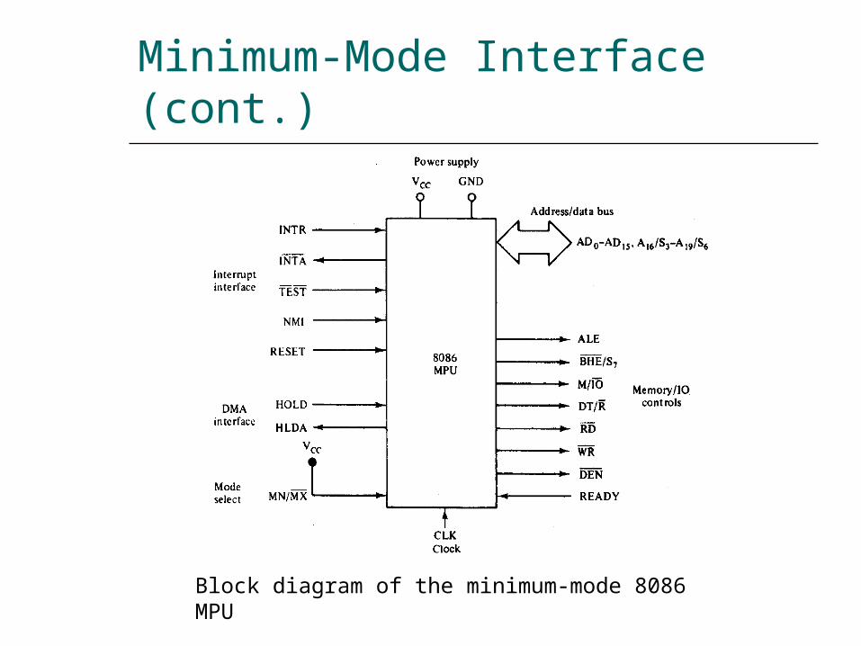
Minimum-Mode Interface (cont)
Minimum-Mode Interface (cont)
Maximum-Mode Interface
The maximum-mode configuration is mainly used for implementing a multiprocessorcoprocessor system environment Multiple processors exist in the system Each executes its own program
Global resources and local resources The former are common to all processors The latter are assigned to specific processors
In the maximum-mode facilities are provided for implementing allocation of global resources and passing bus control to other microprocessors sharing the system bus
Maximum-Mode Interface (cont)
8088 maximum-mode block diagram
Maximum-Mode Interface (cont)
8086 maximum-mode block diagram
Maximum-Mode Interface (cont)
8288 bus controller
Block diagram and pin layout of 8288
Maximum-Mode Interface (cont)
8288 bus controller In the maximum-mode 80888086 outputs a
status code on three signal line S0 S1 S2 prior to the initialization of each bus cycle
The 3-bit bus status code identifies which type of bus cycle is to follow and are input to the external bus controller device 8288
The 8288 produces one or two command signals for each bus cycle
Maximum-Mode Interface (cont)
8288 bus controller
Bus status code
Maximum-Mode Interface (cont)
Maximum-Mode Interface (cont)
Maximum-Mode Interface (cont)
Queue status signals The 2-bit queue status code QS0 and QS1 tells
the external circuitry what type of information was removed form the queue during the previous clock cycle
Queue status code
Electrical Characteristics
Power is applied between pin 40 (Vcc) and pins 1 (GND) and 20 (GND)
The nominal value of Vcc is specified as +5V dc with a tolerance of plusmn10
Both 8088 and 8086 draw a maximum of 340mA from the supply
IO voltage levels
System Clock
The time base for synchronization of the internal and external operations of the microprocessor in a microcomputer system is provided by the clock (CLK) input signal The standard 8088 operates at 5 MHz and the
8088-2 operates at 8 MHz The 8086 is manufactured in three speeds 5-
MHz 8086 8-MHz 8086-2 and the 10-MHz 8086-1
The CLK is externally generated by the 8284 clock generator and driver IC
System Clock (cont)
Block diagram of the 8284 clock generator
System Clock (cont)
Block diagram of the 8284 clock generator
System Clock (cont)
Connecting the 8284 to the 8088
15- or 24MHzcrystal
Typical value of CL when used with 15MHz crystal is 12pF
The fundamental crystal frequency is divided by 3 within the 8284 to give either a 5- or 8-MHz clock signal
System Clock (cont)
CLK waveform The signal is specified at Metal Oxide
Semiconductor (MOS)-compatible voltage level The period of the 5-MHz 8088 can range from
200 ns to 500 ns and the maximum rise and fall times of its edges equal 10 ns
System Clock (cont)
PCLK and OSC signals The peripheral clock (PCLK) and oscillator clock
(OSC) signals are provided to drive peripheral ICs The clock output at PCLK is half the frequency of
CLK The OSC output is at the crystal frequency which is three times of CLK
System Clock (cont)
The 8284 can also be driven from an external clock source Applied to the EFI (External Frequency Input) Input FC is used for selection
0 crystal between X1 and X2 is used 1 selects EFI
The CSYNC input is used for external synchronization in systems with multiple clocks
System Clock (cont)
EXAMPLE If the CLK input of an 8086 MPU is to be driven by
a 9-MHz signal what speed version of the 8086 must be used and what frequency crystal must be attached to the 8284
Solution The 8086-1 is the version of the 8086 that can be
run at 9-MHz To create the 9-MHz clock a 27-MHz crystal must be used on the 8284
Bus Cycle and Time States
A bus cycle defines the basic operation that a microprocessor performs to communicate with external devices
Examples of bus cycles are the memory read memory write inputoutput read and inputoutput write
The bus cycle of the 8088 and 8086 microprocessors consists of at least four clock periods
If no bus cycles are required the microprocessor performs what are known as idle states
When READY is held at the 0 level wait states are inserted between states T3 and T4 of the bus cycle
Bus Cycle and Time States (cont)
Bus cycle clock periods idle state and wait state
Bus Cycle and Time States (cont)
EXAMPLE What is the duration of the bus cycle in the 8088-
based microcomputer if the clock is 8 MHz and the two wait states are inserted
Solution The duration of the bus cycle in an 8 MHz system
is given by tcyc = 500 ns + N x 125 ns
In this expression the N stands for the number of waits states For a bus cycle with two wait states we get
tcyc = 500 ns + 2 x 125 ns = 500 ns + 250 ns = 750 ns
Hardware Organization of the Memory Address Space
1Mx8 memory bank of the 8088
Hardware Organization of the Memory Address Space (cont)
High and low memory banks of the 8086
Hardware Organization of the Memory Address Space (cont)
Byte transfer by the 8088
Hardware Organization of the Memory Address Space (cont)
Word transfer by the 8088
Hardware Organization of the Memory Address Space (cont)
Even address byte transfer by the 8086
Hardware Organization of the Memory Address Space (cont)
Odd address byte transfer by the 8086
Hardware Organization of the Memory Address Space (cont)
Even address word transfer by the 8086
Hardware Organization of the Memory Address Space (cont)
Odd-address word transfer by the 8086
Hardware Organization of the Memory Address Space (cont)
EXAMPLE Is the word at memory address 0123116 of an
8086-based microcomputer aligned or misaligned How many cycle are required to read it from memory
Solution The first byte of the word is the second byte at
the aligned-word address 0123016 Therefore the word is misaligned and required two bus cycles to be read from memory
Address Bus Status Codes
Whenever a memory bus cycle is in progress an address bus status code S4S3 is output by the processor S4S3 identifies which one of the four segment
register is used to generate the physical address in the current bus cycle 1048729
S4S3=00 identifies the extra segment register (ES)
S4S3=01 identifies the stack segment register (SS)
S4S3=10 identifies the code segment register (CS)
S4S3=11 identifies the data segment register (DS)
The memory address reach of the microprocessor can thus be expanded to 4 Mbytes
Memory Control Signals
Minimum-mode memory control signals
Memory Control Signals (cont)
Minimum-mode memory control signals (8088) ALE ndash Address Latch Enable ndash used to latch
the address in external memory IOM ndash Input-OutputMemory ndash signal external
circuitry whether a memory of IO bus cycle is in progress
DTR ndash Data TransmitReceive ndash signal external circuitry whether the 8088 is transmitting or receiving data over the bus 1048729
RD ndash Read ndash identifies that a read bus cycle is in progress
WR ndash Write ndash identifies that a write bus cycle is in progress
DEN ndash Data Enable ndash used to enable the data bus 1048729
SSO ndash Status Line ndash identifies whether a code or data access is in progress
Memory Control Signals (cont)
The control signals for the 8086rsquos minimum-mode memory interface differs in three ways IOM signal is replaced by MIO signal The signal SSO is removed from the interface BHE (bank high enable) is added to the interface
and is used to select input for the high bank of memory in the 8086rsquos memory subsystem
Memory Control Signals (cont)
Maximum-mode memory control signals
Memory Control Signals (cont)
Maximum-mode memory control signals MRDC ndash Memory Read Command 1048729 MWTC ndash Memory Write Command 1048729 AMWC ndash Advanced Memory Write Command
Read and Write Bus Cycle
Read cycle
Minimum-mode memory read bus cycle of the 8088
Read and Write Bus Cycle (cont)
Read cycle
Minimum-mode memory read bus cycle of the 8086
Read and Write Bus Cycle (cont)
Read cycle
Maximum-mode memory read bus cycle of the 8086
Read and Write Bus Cycle (cont)
Write cycle
Minimum-mode memory write bus cycle of the 8088
Read and Write Bus Cycle (cont)
Write cycle
Maximum-mode memory write bus cycle of the 8086
Memory Interface Circuit
Address bus latches and buffers Bank write and bank read control logic Data bus transceiversbuffers Address decoders
Memory Interface Circuit (cont)
Memory interface block diagram
Memory Interface Circuit (cont)
Address bus latches and buffers
Block diagram of a D-type latch
Memory Interface Circuit (cont)
Address bus latches and buffers
Circuit diagram of the 74F373
Memory Interface Circuit (cont)
A review of flip-floplatch logic
Positive edge-triggered D flip-flop
Memory Interface Circuit (cont)
A review of flip-floplatch logic
Positive edge-triggered JK flip-flop
Memory Interface Circuit (cont)
A review of flip-floplatch logic
D-type latch
Memory Interface Circuit (cont)
Address bus latches and buffers
Address latch circuit
Memory Interface Circuit (cont)
Bank write and bank read control logic
Bank write control logic Bank read control logic
Memory Interface Circuit (cont)
Data bus transceivers
Block diagram and circuit diagram of the 74F245 octal bus transceiver
Memory Interface Circuit (cont)
Data bus transceivers
Data bus transceiver circuit
Memory Interface Circuit (cont)
Address decoder
Address bus configuration with address decoding
Memory Interface Circuit (cont)
Address decoder
Block diagram and operation of the 74F139 decoder
Memory Interface Circuit (cont)
Address decoder
Circuit diagram of the 74F139 decoder
Memory Interface Circuit (cont)
Address decoder
Address decoder circuit using 74F139
Memory Interface Circuit (cont)
Address decoder
Block diagram and operation of the 74F138 decoder
Memory Interface Circuit (cont)
Address decoder
Circuit diagram of the 74F138 decoder
Memory Interface Circuit (cont)
Address decoder
Address decoder circuit using 74F138
Types of InputOutput
The IO system allows peripherals to provide data or receive results of processing the data Using IO ports
The 80888086 MPU can employ two types of IO Isolated IO Memory-mapped IO
They differ in how IO ports are mapped into the address space
Types of InputOutput (cont)
Isolated inputoutput When using isolated IO in a microcomputer
system the IO device are treated separate from memory
The memory address space contains 1 M consecutive byte address in the range 0000016 through FFFFF16
The IO address space contains 64K consecutive byte addresses in the range 000016 through FFFF16
The bytes in two consecutive IO addresses can be accessed as word-wide data
Page 0 000016 00FF16
Certain IO instructions can only perform in this range
Types of InputOutput (cont)
Isolated inputoutput
80888086 memory and IO address spaces
Types of InputOutput (cont)
Isolated inputoutput
Isolated IO ports
Types of InputOutput (cont)
Isolated inputoutput Advantages
The complete 1Mbyte memory address space is available for use with memory
Special instructions have been provided to perform IO operations with maximized performance
The bytes in two consecutive IO addresses can be accessed as word-wide data
Disadvantages All input and output data transfers must take place
between the AL or AX register and IO port
Types of InputOutput (cont)
Memory-mapped inputoutput MPU looks at the IO port as though it is a storage
location in memory Some of the memory address space is dedicated to IO
ports Instructions that affect data in memory are used
instead of the special IO instructions More instructions and addressing modes are available to
perform IO operations IO transfers can take place between IO port and other
internal registers The memory instructions tend to execute slower
than those specifically designed for isolated IO Part of the memory address space is lost
Types of InputOutput(cont)
Memory-mapped inputoutput
Memory mapped IO ports
Isolated InputOutput Interface
IO devices Keyboard Printer Mouse 82C55A etc
Functions of interface circuit Select the IO port Latch output data Sample input data Synchronize data transfer Translate between TTL voltage levels and those
required to operate the IO devices
Isolated InputOutput Interface (cont)
Minimum-mode interface
Minimum-mode 8088 system IO interface
Isolated InputOutput Interface (cont)
Minimum-mode interface
Minimum-mode 8086 system IO interface
Isolated InputOutput Interface (cont)
Maximum-mode interface
Maximum-mode 8088 system IO interface
Isolated InputOutput Interface (cont)
Maximum-mode interface
Maximum-mode 8086 system IO interface
Isolated InputOutput Interface (cont)
Maximum-mode interface
IO bus cycle status codes
InputOutput Data Transfer
Inputoutput data transfers in the 8088 and 8086 microcomputers can be either byte-wide or word-wide
IO addresses are 16 bits in length and are output by the 8088 to the IO interface over bus lines AD0 through AD7 and A8 through A15
In 8088 the word transfers is performed as two consecutive byte-wide data transfer and takes two bus cycle
In 8086 the word transfers can takes either one or two bus cycle
Word-wide IO ports should be aligned at even-address boundaries
InputOutput Data Instructions
InputOutput Data Instructions(cont)
EXAMPLE Write a sequence of instructions that will output
the data FF16 to a byte-wide output port at address AB16 of the IO address space
Solution First the AL register is loaded with FF16 as an
immediate operand in the instruction
MOV AL 0FFH Now the data in AL can be output to the byte-
wide output port with the instruction
OUT 0ABH AL
InputOutput Data Instructions(cont)
EXAMPLE Write a series of instructions that will output FF16 to an
output port located at address B00016 of the IO address space
Solution The DX register must first be loaded with the address
of the output port This is done with the instructionMOV DX 0B000H
Next the data that are to be output must be loaded into AL with the instruction
MOV AL 0FFH Finally the data are output with the instruction
OUT DX AL
InputOutput Data Instructions(cont)
EXAMPLE Data are to be read in from two byte-wide input
ports at addresses AA16 and A916 and then output as a word-wide output port at address B00016 Write a sequence of instructions to perform this inputoutput operation
InputOutput Data Instructions(cont)
Solution First read in the byte at address AA16 into AL and
move it into AHIN AL 0AAHMOV AH AL
Now the other byte can be read into AL by the instructionIN AL 09AH
And to write out the word of dataMOV DX 0B000HOUT DX AX
InputOutput Bus Cycles
Input bus cycle of the 8088
InputOutput Bus Cycles (cont)
Output bus cycle of the 8088
InputOutput Bus Cycles (cont)
Input bus cycle of the 8086
InputOutput Bus Cycles (cont)
Output bus cycle of the 8086
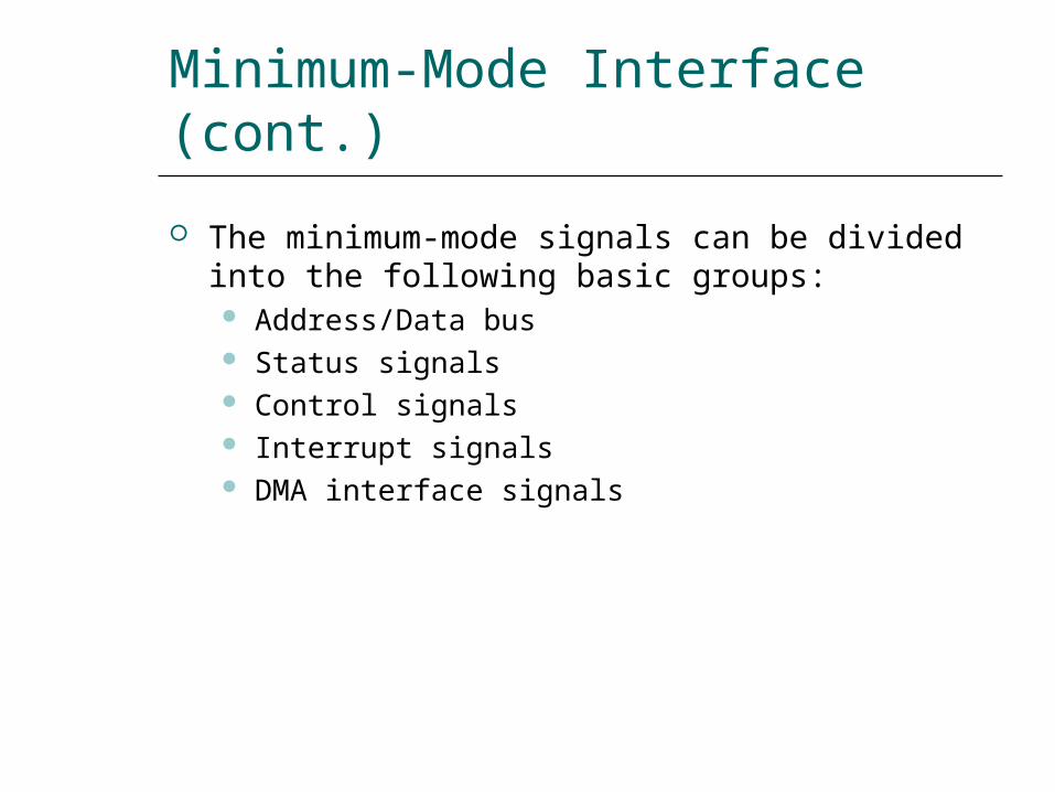
Minimum-Mode Interface (cont)
Maximum-Mode Interface
The maximum-mode configuration is mainly used for implementing a multiprocessorcoprocessor system environment Multiple processors exist in the system Each executes its own program
Global resources and local resources The former are common to all processors The latter are assigned to specific processors
In the maximum-mode facilities are provided for implementing allocation of global resources and passing bus control to other microprocessors sharing the system bus
Maximum-Mode Interface (cont)
8088 maximum-mode block diagram
Maximum-Mode Interface (cont)
8086 maximum-mode block diagram
Maximum-Mode Interface (cont)
8288 bus controller
Block diagram and pin layout of 8288
Maximum-Mode Interface (cont)
8288 bus controller In the maximum-mode 80888086 outputs a
status code on three signal line S0 S1 S2 prior to the initialization of each bus cycle
The 3-bit bus status code identifies which type of bus cycle is to follow and are input to the external bus controller device 8288
The 8288 produces one or two command signals for each bus cycle
Maximum-Mode Interface (cont)
8288 bus controller
Bus status code
Maximum-Mode Interface (cont)
Maximum-Mode Interface (cont)
Maximum-Mode Interface (cont)
Queue status signals The 2-bit queue status code QS0 and QS1 tells
the external circuitry what type of information was removed form the queue during the previous clock cycle
Queue status code
Electrical Characteristics
Power is applied between pin 40 (Vcc) and pins 1 (GND) and 20 (GND)
The nominal value of Vcc is specified as +5V dc with a tolerance of plusmn10
Both 8088 and 8086 draw a maximum of 340mA from the supply
IO voltage levels
System Clock
The time base for synchronization of the internal and external operations of the microprocessor in a microcomputer system is provided by the clock (CLK) input signal The standard 8088 operates at 5 MHz and the
8088-2 operates at 8 MHz The 8086 is manufactured in three speeds 5-
MHz 8086 8-MHz 8086-2 and the 10-MHz 8086-1
The CLK is externally generated by the 8284 clock generator and driver IC
System Clock (cont)
Block diagram of the 8284 clock generator
System Clock (cont)
Block diagram of the 8284 clock generator
System Clock (cont)
Connecting the 8284 to the 8088
15- or 24MHzcrystal
Typical value of CL when used with 15MHz crystal is 12pF
The fundamental crystal frequency is divided by 3 within the 8284 to give either a 5- or 8-MHz clock signal
System Clock (cont)
CLK waveform The signal is specified at Metal Oxide
Semiconductor (MOS)-compatible voltage level The period of the 5-MHz 8088 can range from
200 ns to 500 ns and the maximum rise and fall times of its edges equal 10 ns
System Clock (cont)
PCLK and OSC signals The peripheral clock (PCLK) and oscillator clock
(OSC) signals are provided to drive peripheral ICs The clock output at PCLK is half the frequency of
CLK The OSC output is at the crystal frequency which is three times of CLK
System Clock (cont)
The 8284 can also be driven from an external clock source Applied to the EFI (External Frequency Input) Input FC is used for selection
0 crystal between X1 and X2 is used 1 selects EFI
The CSYNC input is used for external synchronization in systems with multiple clocks
System Clock (cont)
EXAMPLE If the CLK input of an 8086 MPU is to be driven by
a 9-MHz signal what speed version of the 8086 must be used and what frequency crystal must be attached to the 8284
Solution The 8086-1 is the version of the 8086 that can be
run at 9-MHz To create the 9-MHz clock a 27-MHz crystal must be used on the 8284
Bus Cycle and Time States
A bus cycle defines the basic operation that a microprocessor performs to communicate with external devices
Examples of bus cycles are the memory read memory write inputoutput read and inputoutput write
The bus cycle of the 8088 and 8086 microprocessors consists of at least four clock periods
If no bus cycles are required the microprocessor performs what are known as idle states
When READY is held at the 0 level wait states are inserted between states T3 and T4 of the bus cycle
Bus Cycle and Time States (cont)
Bus cycle clock periods idle state and wait state
Bus Cycle and Time States (cont)
EXAMPLE What is the duration of the bus cycle in the 8088-
based microcomputer if the clock is 8 MHz and the two wait states are inserted
Solution The duration of the bus cycle in an 8 MHz system
is given by tcyc = 500 ns + N x 125 ns
In this expression the N stands for the number of waits states For a bus cycle with two wait states we get
tcyc = 500 ns + 2 x 125 ns = 500 ns + 250 ns = 750 ns
Hardware Organization of the Memory Address Space
1Mx8 memory bank of the 8088
Hardware Organization of the Memory Address Space (cont)
High and low memory banks of the 8086
Hardware Organization of the Memory Address Space (cont)
Byte transfer by the 8088
Hardware Organization of the Memory Address Space (cont)
Word transfer by the 8088
Hardware Organization of the Memory Address Space (cont)
Even address byte transfer by the 8086
Hardware Organization of the Memory Address Space (cont)
Odd address byte transfer by the 8086
Hardware Organization of the Memory Address Space (cont)
Even address word transfer by the 8086
Hardware Organization of the Memory Address Space (cont)
Odd-address word transfer by the 8086
Hardware Organization of the Memory Address Space (cont)
EXAMPLE Is the word at memory address 0123116 of an
8086-based microcomputer aligned or misaligned How many cycle are required to read it from memory
Solution The first byte of the word is the second byte at
the aligned-word address 0123016 Therefore the word is misaligned and required two bus cycles to be read from memory
Address Bus Status Codes
Whenever a memory bus cycle is in progress an address bus status code S4S3 is output by the processor S4S3 identifies which one of the four segment
register is used to generate the physical address in the current bus cycle 1048729
S4S3=00 identifies the extra segment register (ES)
S4S3=01 identifies the stack segment register (SS)
S4S3=10 identifies the code segment register (CS)
S4S3=11 identifies the data segment register (DS)
The memory address reach of the microprocessor can thus be expanded to 4 Mbytes
Memory Control Signals
Minimum-mode memory control signals
Memory Control Signals (cont)
Minimum-mode memory control signals (8088) ALE ndash Address Latch Enable ndash used to latch
the address in external memory IOM ndash Input-OutputMemory ndash signal external
circuitry whether a memory of IO bus cycle is in progress
DTR ndash Data TransmitReceive ndash signal external circuitry whether the 8088 is transmitting or receiving data over the bus 1048729
RD ndash Read ndash identifies that a read bus cycle is in progress
WR ndash Write ndash identifies that a write bus cycle is in progress
DEN ndash Data Enable ndash used to enable the data bus 1048729
SSO ndash Status Line ndash identifies whether a code or data access is in progress
Memory Control Signals (cont)
The control signals for the 8086rsquos minimum-mode memory interface differs in three ways IOM signal is replaced by MIO signal The signal SSO is removed from the interface BHE (bank high enable) is added to the interface
and is used to select input for the high bank of memory in the 8086rsquos memory subsystem
Memory Control Signals (cont)
Maximum-mode memory control signals
Memory Control Signals (cont)
Maximum-mode memory control signals MRDC ndash Memory Read Command 1048729 MWTC ndash Memory Write Command 1048729 AMWC ndash Advanced Memory Write Command
Read and Write Bus Cycle
Read cycle
Minimum-mode memory read bus cycle of the 8088
Read and Write Bus Cycle (cont)
Read cycle
Minimum-mode memory read bus cycle of the 8086
Read and Write Bus Cycle (cont)
Read cycle
Maximum-mode memory read bus cycle of the 8086
Read and Write Bus Cycle (cont)
Write cycle
Minimum-mode memory write bus cycle of the 8088
Read and Write Bus Cycle (cont)
Write cycle
Maximum-mode memory write bus cycle of the 8086
Memory Interface Circuit
Address bus latches and buffers Bank write and bank read control logic Data bus transceiversbuffers Address decoders
Memory Interface Circuit (cont)
Memory interface block diagram
Memory Interface Circuit (cont)
Address bus latches and buffers
Block diagram of a D-type latch
Memory Interface Circuit (cont)
Address bus latches and buffers
Circuit diagram of the 74F373
Memory Interface Circuit (cont)
A review of flip-floplatch logic
Positive edge-triggered D flip-flop
Memory Interface Circuit (cont)
A review of flip-floplatch logic
Positive edge-triggered JK flip-flop
Memory Interface Circuit (cont)
A review of flip-floplatch logic
D-type latch
Memory Interface Circuit (cont)
Address bus latches and buffers
Address latch circuit
Memory Interface Circuit (cont)
Bank write and bank read control logic
Bank write control logic Bank read control logic
Memory Interface Circuit (cont)
Data bus transceivers
Block diagram and circuit diagram of the 74F245 octal bus transceiver
Memory Interface Circuit (cont)
Data bus transceivers
Data bus transceiver circuit
Memory Interface Circuit (cont)
Address decoder
Address bus configuration with address decoding
Memory Interface Circuit (cont)
Address decoder
Block diagram and operation of the 74F139 decoder
Memory Interface Circuit (cont)
Address decoder
Circuit diagram of the 74F139 decoder
Memory Interface Circuit (cont)
Address decoder
Address decoder circuit using 74F139
Memory Interface Circuit (cont)
Address decoder
Block diagram and operation of the 74F138 decoder
Memory Interface Circuit (cont)
Address decoder
Circuit diagram of the 74F138 decoder
Memory Interface Circuit (cont)
Address decoder
Address decoder circuit using 74F138
Types of InputOutput
The IO system allows peripherals to provide data or receive results of processing the data Using IO ports
The 80888086 MPU can employ two types of IO Isolated IO Memory-mapped IO
They differ in how IO ports are mapped into the address space
Types of InputOutput (cont)
Isolated inputoutput When using isolated IO in a microcomputer
system the IO device are treated separate from memory
The memory address space contains 1 M consecutive byte address in the range 0000016 through FFFFF16
The IO address space contains 64K consecutive byte addresses in the range 000016 through FFFF16
The bytes in two consecutive IO addresses can be accessed as word-wide data
Page 0 000016 00FF16
Certain IO instructions can only perform in this range
Types of InputOutput (cont)
Isolated inputoutput
80888086 memory and IO address spaces
Types of InputOutput (cont)
Isolated inputoutput
Isolated IO ports
Types of InputOutput (cont)
Isolated inputoutput Advantages
The complete 1Mbyte memory address space is available for use with memory
Special instructions have been provided to perform IO operations with maximized performance
The bytes in two consecutive IO addresses can be accessed as word-wide data
Disadvantages All input and output data transfers must take place
between the AL or AX register and IO port
Types of InputOutput (cont)
Memory-mapped inputoutput MPU looks at the IO port as though it is a storage
location in memory Some of the memory address space is dedicated to IO
ports Instructions that affect data in memory are used
instead of the special IO instructions More instructions and addressing modes are available to
perform IO operations IO transfers can take place between IO port and other
internal registers The memory instructions tend to execute slower
than those specifically designed for isolated IO Part of the memory address space is lost
Types of InputOutput(cont)
Memory-mapped inputoutput
Memory mapped IO ports
Isolated InputOutput Interface
IO devices Keyboard Printer Mouse 82C55A etc
Functions of interface circuit Select the IO port Latch output data Sample input data Synchronize data transfer Translate between TTL voltage levels and those
required to operate the IO devices
Isolated InputOutput Interface (cont)
Minimum-mode interface
Minimum-mode 8088 system IO interface
Isolated InputOutput Interface (cont)
Minimum-mode interface
Minimum-mode 8086 system IO interface
Isolated InputOutput Interface (cont)
Maximum-mode interface
Maximum-mode 8088 system IO interface
Isolated InputOutput Interface (cont)
Maximum-mode interface
Maximum-mode 8086 system IO interface
Isolated InputOutput Interface (cont)
Maximum-mode interface
IO bus cycle status codes
InputOutput Data Transfer
Inputoutput data transfers in the 8088 and 8086 microcomputers can be either byte-wide or word-wide
IO addresses are 16 bits in length and are output by the 8088 to the IO interface over bus lines AD0 through AD7 and A8 through A15
In 8088 the word transfers is performed as two consecutive byte-wide data transfer and takes two bus cycle
In 8086 the word transfers can takes either one or two bus cycle
Word-wide IO ports should be aligned at even-address boundaries
InputOutput Data Instructions
InputOutput Data Instructions(cont)
EXAMPLE Write a sequence of instructions that will output
the data FF16 to a byte-wide output port at address AB16 of the IO address space
Solution First the AL register is loaded with FF16 as an
immediate operand in the instruction
MOV AL 0FFH Now the data in AL can be output to the byte-
wide output port with the instruction
OUT 0ABH AL
InputOutput Data Instructions(cont)
EXAMPLE Write a series of instructions that will output FF16 to an
output port located at address B00016 of the IO address space
Solution The DX register must first be loaded with the address
of the output port This is done with the instructionMOV DX 0B000H
Next the data that are to be output must be loaded into AL with the instruction
MOV AL 0FFH Finally the data are output with the instruction
OUT DX AL
InputOutput Data Instructions(cont)
EXAMPLE Data are to be read in from two byte-wide input
ports at addresses AA16 and A916 and then output as a word-wide output port at address B00016 Write a sequence of instructions to perform this inputoutput operation
InputOutput Data Instructions(cont)
Solution First read in the byte at address AA16 into AL and
move it into AHIN AL 0AAHMOV AH AL
Now the other byte can be read into AL by the instructionIN AL 09AH
And to write out the word of dataMOV DX 0B000HOUT DX AX
InputOutput Bus Cycles
Input bus cycle of the 8088
InputOutput Bus Cycles (cont)
Output bus cycle of the 8088
InputOutput Bus Cycles (cont)
Input bus cycle of the 8086
InputOutput Bus Cycles (cont)
Output bus cycle of the 8086
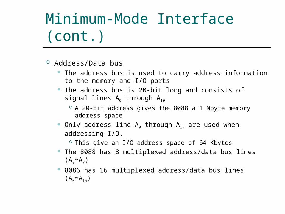
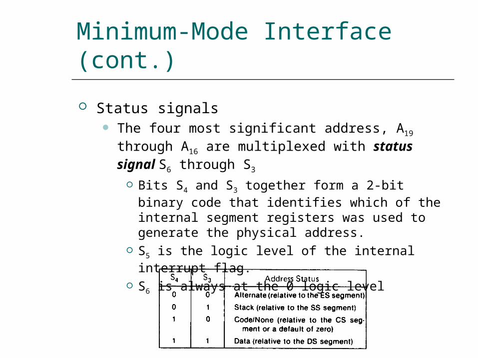
Maximum-Mode Interface (cont)
8088 maximum-mode block diagram
Maximum-Mode Interface (cont)
8086 maximum-mode block diagram
Maximum-Mode Interface (cont)
8288 bus controller
Block diagram and pin layout of 8288
Maximum-Mode Interface (cont)
8288 bus controller In the maximum-mode 80888086 outputs a
status code on three signal line S0 S1 S2 prior to the initialization of each bus cycle
The 3-bit bus status code identifies which type of bus cycle is to follow and are input to the external bus controller device 8288
The 8288 produces one or two command signals for each bus cycle
Maximum-Mode Interface (cont)
8288 bus controller
Bus status code
Maximum-Mode Interface (cont)
Maximum-Mode Interface (cont)
Maximum-Mode Interface (cont)
Queue status signals The 2-bit queue status code QS0 and QS1 tells
the external circuitry what type of information was removed form the queue during the previous clock cycle
Queue status code
Electrical Characteristics
Power is applied between pin 40 (Vcc) and pins 1 (GND) and 20 (GND)
The nominal value of Vcc is specified as +5V dc with a tolerance of plusmn10
Both 8088 and 8086 draw a maximum of 340mA from the supply
IO voltage levels
System Clock
The time base for synchronization of the internal and external operations of the microprocessor in a microcomputer system is provided by the clock (CLK) input signal The standard 8088 operates at 5 MHz and the
8088-2 operates at 8 MHz The 8086 is manufactured in three speeds 5-
MHz 8086 8-MHz 8086-2 and the 10-MHz 8086-1
The CLK is externally generated by the 8284 clock generator and driver IC
System Clock (cont)
Block diagram of the 8284 clock generator
System Clock (cont)
Block diagram of the 8284 clock generator
System Clock (cont)
Connecting the 8284 to the 8088
15- or 24MHzcrystal
Typical value of CL when used with 15MHz crystal is 12pF
The fundamental crystal frequency is divided by 3 within the 8284 to give either a 5- or 8-MHz clock signal
System Clock (cont)
CLK waveform The signal is specified at Metal Oxide
Semiconductor (MOS)-compatible voltage level The period of the 5-MHz 8088 can range from
200 ns to 500 ns and the maximum rise and fall times of its edges equal 10 ns
System Clock (cont)
PCLK and OSC signals The peripheral clock (PCLK) and oscillator clock
(OSC) signals are provided to drive peripheral ICs The clock output at PCLK is half the frequency of
CLK The OSC output is at the crystal frequency which is three times of CLK
System Clock (cont)
The 8284 can also be driven from an external clock source Applied to the EFI (External Frequency Input) Input FC is used for selection
0 crystal between X1 and X2 is used 1 selects EFI
The CSYNC input is used for external synchronization in systems with multiple clocks
System Clock (cont)
EXAMPLE If the CLK input of an 8086 MPU is to be driven by
a 9-MHz signal what speed version of the 8086 must be used and what frequency crystal must be attached to the 8284
Solution The 8086-1 is the version of the 8086 that can be
run at 9-MHz To create the 9-MHz clock a 27-MHz crystal must be used on the 8284
Bus Cycle and Time States
A bus cycle defines the basic operation that a microprocessor performs to communicate with external devices
Examples of bus cycles are the memory read memory write inputoutput read and inputoutput write
The bus cycle of the 8088 and 8086 microprocessors consists of at least four clock periods
If no bus cycles are required the microprocessor performs what are known as idle states
When READY is held at the 0 level wait states are inserted between states T3 and T4 of the bus cycle
Bus Cycle and Time States (cont)
Bus cycle clock periods idle state and wait state
Bus Cycle and Time States (cont)
EXAMPLE What is the duration of the bus cycle in the 8088-
based microcomputer if the clock is 8 MHz and the two wait states are inserted
Solution The duration of the bus cycle in an 8 MHz system
is given by tcyc = 500 ns + N x 125 ns
In this expression the N stands for the number of waits states For a bus cycle with two wait states we get
tcyc = 500 ns + 2 x 125 ns = 500 ns + 250 ns = 750 ns
Hardware Organization of the Memory Address Space
1Mx8 memory bank of the 8088
Hardware Organization of the Memory Address Space (cont)
High and low memory banks of the 8086
Hardware Organization of the Memory Address Space (cont)
Byte transfer by the 8088
Hardware Organization of the Memory Address Space (cont)
Word transfer by the 8088
Hardware Organization of the Memory Address Space (cont)
Even address byte transfer by the 8086
Hardware Organization of the Memory Address Space (cont)
Odd address byte transfer by the 8086
Hardware Organization of the Memory Address Space (cont)
Even address word transfer by the 8086
Hardware Organization of the Memory Address Space (cont)
Odd-address word transfer by the 8086
Hardware Organization of the Memory Address Space (cont)
EXAMPLE Is the word at memory address 0123116 of an
8086-based microcomputer aligned or misaligned How many cycle are required to read it from memory
Solution The first byte of the word is the second byte at
the aligned-word address 0123016 Therefore the word is misaligned and required two bus cycles to be read from memory
Address Bus Status Codes
Whenever a memory bus cycle is in progress an address bus status code S4S3 is output by the processor S4S3 identifies which one of the four segment
register is used to generate the physical address in the current bus cycle 1048729
S4S3=00 identifies the extra segment register (ES)
S4S3=01 identifies the stack segment register (SS)
S4S3=10 identifies the code segment register (CS)
S4S3=11 identifies the data segment register (DS)
The memory address reach of the microprocessor can thus be expanded to 4 Mbytes
Memory Control Signals
Minimum-mode memory control signals
Memory Control Signals (cont)
Minimum-mode memory control signals (8088) ALE ndash Address Latch Enable ndash used to latch
the address in external memory IOM ndash Input-OutputMemory ndash signal external
circuitry whether a memory of IO bus cycle is in progress
DTR ndash Data TransmitReceive ndash signal external circuitry whether the 8088 is transmitting or receiving data over the bus 1048729
RD ndash Read ndash identifies that a read bus cycle is in progress
WR ndash Write ndash identifies that a write bus cycle is in progress
DEN ndash Data Enable ndash used to enable the data bus 1048729
SSO ndash Status Line ndash identifies whether a code or data access is in progress
Memory Control Signals (cont)
The control signals for the 8086rsquos minimum-mode memory interface differs in three ways IOM signal is replaced by MIO signal The signal SSO is removed from the interface BHE (bank high enable) is added to the interface
and is used to select input for the high bank of memory in the 8086rsquos memory subsystem
Memory Control Signals (cont)
Maximum-mode memory control signals
Memory Control Signals (cont)
Maximum-mode memory control signals MRDC ndash Memory Read Command 1048729 MWTC ndash Memory Write Command 1048729 AMWC ndash Advanced Memory Write Command
Read and Write Bus Cycle
Read cycle
Minimum-mode memory read bus cycle of the 8088
Read and Write Bus Cycle (cont)
Read cycle
Minimum-mode memory read bus cycle of the 8086
Read and Write Bus Cycle (cont)
Read cycle
Maximum-mode memory read bus cycle of the 8086
Read and Write Bus Cycle (cont)
Write cycle
Minimum-mode memory write bus cycle of the 8088
Read and Write Bus Cycle (cont)
Write cycle
Maximum-mode memory write bus cycle of the 8086
Memory Interface Circuit
Address bus latches and buffers Bank write and bank read control logic Data bus transceiversbuffers Address decoders
Memory Interface Circuit (cont)
Memory interface block diagram
Memory Interface Circuit (cont)
Address bus latches and buffers
Block diagram of a D-type latch
Memory Interface Circuit (cont)
Address bus latches and buffers
Circuit diagram of the 74F373
Memory Interface Circuit (cont)
A review of flip-floplatch logic
Positive edge-triggered D flip-flop
Memory Interface Circuit (cont)
A review of flip-floplatch logic
Positive edge-triggered JK flip-flop
Memory Interface Circuit (cont)
A review of flip-floplatch logic
D-type latch
Memory Interface Circuit (cont)
Address bus latches and buffers
Address latch circuit
Memory Interface Circuit (cont)
Bank write and bank read control logic
Bank write control logic Bank read control logic
Memory Interface Circuit (cont)
Data bus transceivers
Block diagram and circuit diagram of the 74F245 octal bus transceiver
Memory Interface Circuit (cont)
Data bus transceivers
Data bus transceiver circuit
Memory Interface Circuit (cont)
Address decoder
Address bus configuration with address decoding
Memory Interface Circuit (cont)
Address decoder
Block diagram and operation of the 74F139 decoder
Memory Interface Circuit (cont)
Address decoder
Circuit diagram of the 74F139 decoder
Memory Interface Circuit (cont)
Address decoder
Address decoder circuit using 74F139
Memory Interface Circuit (cont)
Address decoder
Block diagram and operation of the 74F138 decoder
Memory Interface Circuit (cont)
Address decoder
Circuit diagram of the 74F138 decoder
Memory Interface Circuit (cont)
Address decoder
Address decoder circuit using 74F138
Types of InputOutput
The IO system allows peripherals to provide data or receive results of processing the data Using IO ports
The 80888086 MPU can employ two types of IO Isolated IO Memory-mapped IO
They differ in how IO ports are mapped into the address space
Types of InputOutput (cont)
Isolated inputoutput When using isolated IO in a microcomputer
system the IO device are treated separate from memory
The memory address space contains 1 M consecutive byte address in the range 0000016 through FFFFF16
The IO address space contains 64K consecutive byte addresses in the range 000016 through FFFF16
The bytes in two consecutive IO addresses can be accessed as word-wide data
Page 0 000016 00FF16
Certain IO instructions can only perform in this range
Types of InputOutput (cont)
Isolated inputoutput
80888086 memory and IO address spaces
Types of InputOutput (cont)
Isolated inputoutput
Isolated IO ports
Types of InputOutput (cont)
Isolated inputoutput Advantages
The complete 1Mbyte memory address space is available for use with memory
Special instructions have been provided to perform IO operations with maximized performance
The bytes in two consecutive IO addresses can be accessed as word-wide data
Disadvantages All input and output data transfers must take place
between the AL or AX register and IO port
Types of InputOutput (cont)
Memory-mapped inputoutput MPU looks at the IO port as though it is a storage
location in memory Some of the memory address space is dedicated to IO
ports Instructions that affect data in memory are used
instead of the special IO instructions More instructions and addressing modes are available to
perform IO operations IO transfers can take place between IO port and other
internal registers The memory instructions tend to execute slower
than those specifically designed for isolated IO Part of the memory address space is lost
Types of InputOutput(cont)
Memory-mapped inputoutput
Memory mapped IO ports
Isolated InputOutput Interface
IO devices Keyboard Printer Mouse 82C55A etc
Functions of interface circuit Select the IO port Latch output data Sample input data Synchronize data transfer Translate between TTL voltage levels and those
required to operate the IO devices
Isolated InputOutput Interface (cont)
Minimum-mode interface
Minimum-mode 8088 system IO interface
Isolated InputOutput Interface (cont)
Minimum-mode interface
Minimum-mode 8086 system IO interface
Isolated InputOutput Interface (cont)
Maximum-mode interface
Maximum-mode 8088 system IO interface
Isolated InputOutput Interface (cont)
Maximum-mode interface
Maximum-mode 8086 system IO interface
Isolated InputOutput Interface (cont)
Maximum-mode interface
IO bus cycle status codes
InputOutput Data Transfer
Inputoutput data transfers in the 8088 and 8086 microcomputers can be either byte-wide or word-wide
IO addresses are 16 bits in length and are output by the 8088 to the IO interface over bus lines AD0 through AD7 and A8 through A15
In 8088 the word transfers is performed as two consecutive byte-wide data transfer and takes two bus cycle
In 8086 the word transfers can takes either one or two bus cycle
Word-wide IO ports should be aligned at even-address boundaries
InputOutput Data Instructions
InputOutput Data Instructions(cont)
EXAMPLE Write a sequence of instructions that will output
the data FF16 to a byte-wide output port at address AB16 of the IO address space
Solution First the AL register is loaded with FF16 as an
immediate operand in the instruction
MOV AL 0FFH Now the data in AL can be output to the byte-
wide output port with the instruction
OUT 0ABH AL
InputOutput Data Instructions(cont)
EXAMPLE Write a series of instructions that will output FF16 to an
output port located at address B00016 of the IO address space
Solution The DX register must first be loaded with the address
of the output port This is done with the instructionMOV DX 0B000H
Next the data that are to be output must be loaded into AL with the instruction
MOV AL 0FFH Finally the data are output with the instruction
OUT DX AL
InputOutput Data Instructions(cont)
EXAMPLE Data are to be read in from two byte-wide input
ports at addresses AA16 and A916 and then output as a word-wide output port at address B00016 Write a sequence of instructions to perform this inputoutput operation
InputOutput Data Instructions(cont)
Solution First read in the byte at address AA16 into AL and
move it into AHIN AL 0AAHMOV AH AL
Now the other byte can be read into AL by the instructionIN AL 09AH
And to write out the word of dataMOV DX 0B000HOUT DX AX
InputOutput Bus Cycles
Input bus cycle of the 8088
InputOutput Bus Cycles (cont)
Output bus cycle of the 8088
InputOutput Bus Cycles (cont)
Input bus cycle of the 8086
InputOutput Bus Cycles (cont)
Output bus cycle of the 8086
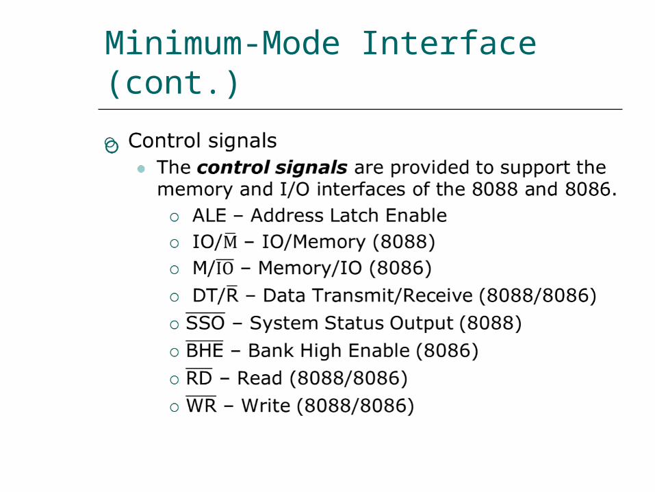
Maximum-Mode Interface (cont)
8086 maximum-mode block diagram
Maximum-Mode Interface (cont)
8288 bus controller
Block diagram and pin layout of 8288
Maximum-Mode Interface (cont)
8288 bus controller In the maximum-mode 80888086 outputs a
status code on three signal line S0 S1 S2 prior to the initialization of each bus cycle
The 3-bit bus status code identifies which type of bus cycle is to follow and are input to the external bus controller device 8288
The 8288 produces one or two command signals for each bus cycle
Maximum-Mode Interface (cont)
8288 bus controller
Bus status code
Maximum-Mode Interface (cont)
Maximum-Mode Interface (cont)
Maximum-Mode Interface (cont)
Queue status signals The 2-bit queue status code QS0 and QS1 tells
the external circuitry what type of information was removed form the queue during the previous clock cycle
Queue status code
Electrical Characteristics
Power is applied between pin 40 (Vcc) and pins 1 (GND) and 20 (GND)
The nominal value of Vcc is specified as +5V dc with a tolerance of plusmn10
Both 8088 and 8086 draw a maximum of 340mA from the supply
IO voltage levels
System Clock
The time base for synchronization of the internal and external operations of the microprocessor in a microcomputer system is provided by the clock (CLK) input signal The standard 8088 operates at 5 MHz and the
8088-2 operates at 8 MHz The 8086 is manufactured in three speeds 5-
MHz 8086 8-MHz 8086-2 and the 10-MHz 8086-1
The CLK is externally generated by the 8284 clock generator and driver IC
System Clock (cont)
Block diagram of the 8284 clock generator
System Clock (cont)
Block diagram of the 8284 clock generator
System Clock (cont)
Connecting the 8284 to the 8088
15- or 24MHzcrystal
Typical value of CL when used with 15MHz crystal is 12pF
The fundamental crystal frequency is divided by 3 within the 8284 to give either a 5- or 8-MHz clock signal
System Clock (cont)
CLK waveform The signal is specified at Metal Oxide
Semiconductor (MOS)-compatible voltage level The period of the 5-MHz 8088 can range from
200 ns to 500 ns and the maximum rise and fall times of its edges equal 10 ns
System Clock (cont)
PCLK and OSC signals The peripheral clock (PCLK) and oscillator clock
(OSC) signals are provided to drive peripheral ICs The clock output at PCLK is half the frequency of
CLK The OSC output is at the crystal frequency which is three times of CLK
System Clock (cont)
The 8284 can also be driven from an external clock source Applied to the EFI (External Frequency Input) Input FC is used for selection
0 crystal between X1 and X2 is used 1 selects EFI
The CSYNC input is used for external synchronization in systems with multiple clocks
System Clock (cont)
EXAMPLE If the CLK input of an 8086 MPU is to be driven by
a 9-MHz signal what speed version of the 8086 must be used and what frequency crystal must be attached to the 8284
Solution The 8086-1 is the version of the 8086 that can be
run at 9-MHz To create the 9-MHz clock a 27-MHz crystal must be used on the 8284
Bus Cycle and Time States
A bus cycle defines the basic operation that a microprocessor performs to communicate with external devices
Examples of bus cycles are the memory read memory write inputoutput read and inputoutput write
The bus cycle of the 8088 and 8086 microprocessors consists of at least four clock periods
If no bus cycles are required the microprocessor performs what are known as idle states
When READY is held at the 0 level wait states are inserted between states T3 and T4 of the bus cycle
Bus Cycle and Time States (cont)
Bus cycle clock periods idle state and wait state
Bus Cycle and Time States (cont)
EXAMPLE What is the duration of the bus cycle in the 8088-
based microcomputer if the clock is 8 MHz and the two wait states are inserted
Solution The duration of the bus cycle in an 8 MHz system
is given by tcyc = 500 ns + N x 125 ns
In this expression the N stands for the number of waits states For a bus cycle with two wait states we get
tcyc = 500 ns + 2 x 125 ns = 500 ns + 250 ns = 750 ns
Hardware Organization of the Memory Address Space
1Mx8 memory bank of the 8088
Hardware Organization of the Memory Address Space (cont)
High and low memory banks of the 8086
Hardware Organization of the Memory Address Space (cont)
Byte transfer by the 8088
Hardware Organization of the Memory Address Space (cont)
Word transfer by the 8088
Hardware Organization of the Memory Address Space (cont)
Even address byte transfer by the 8086
Hardware Organization of the Memory Address Space (cont)
Odd address byte transfer by the 8086
Hardware Organization of the Memory Address Space (cont)
Even address word transfer by the 8086
Hardware Organization of the Memory Address Space (cont)
Odd-address word transfer by the 8086
Hardware Organization of the Memory Address Space (cont)
EXAMPLE Is the word at memory address 0123116 of an
8086-based microcomputer aligned or misaligned How many cycle are required to read it from memory
Solution The first byte of the word is the second byte at
the aligned-word address 0123016 Therefore the word is misaligned and required two bus cycles to be read from memory
Address Bus Status Codes
Whenever a memory bus cycle is in progress an address bus status code S4S3 is output by the processor S4S3 identifies which one of the four segment
register is used to generate the physical address in the current bus cycle 1048729
S4S3=00 identifies the extra segment register (ES)
S4S3=01 identifies the stack segment register (SS)
S4S3=10 identifies the code segment register (CS)
S4S3=11 identifies the data segment register (DS)
The memory address reach of the microprocessor can thus be expanded to 4 Mbytes
Memory Control Signals
Minimum-mode memory control signals
Memory Control Signals (cont)
Minimum-mode memory control signals (8088) ALE ndash Address Latch Enable ndash used to latch
the address in external memory IOM ndash Input-OutputMemory ndash signal external
circuitry whether a memory of IO bus cycle is in progress
DTR ndash Data TransmitReceive ndash signal external circuitry whether the 8088 is transmitting or receiving data over the bus 1048729
RD ndash Read ndash identifies that a read bus cycle is in progress
WR ndash Write ndash identifies that a write bus cycle is in progress
DEN ndash Data Enable ndash used to enable the data bus 1048729
SSO ndash Status Line ndash identifies whether a code or data access is in progress
Memory Control Signals (cont)
The control signals for the 8086rsquos minimum-mode memory interface differs in three ways IOM signal is replaced by MIO signal The signal SSO is removed from the interface BHE (bank high enable) is added to the interface
and is used to select input for the high bank of memory in the 8086rsquos memory subsystem
Memory Control Signals (cont)
Maximum-mode memory control signals
Memory Control Signals (cont)
Maximum-mode memory control signals MRDC ndash Memory Read Command 1048729 MWTC ndash Memory Write Command 1048729 AMWC ndash Advanced Memory Write Command
Read and Write Bus Cycle
Read cycle
Minimum-mode memory read bus cycle of the 8088
Read and Write Bus Cycle (cont)
Read cycle
Minimum-mode memory read bus cycle of the 8086
Read and Write Bus Cycle (cont)
Read cycle
Maximum-mode memory read bus cycle of the 8086
Read and Write Bus Cycle (cont)
Write cycle
Minimum-mode memory write bus cycle of the 8088
Read and Write Bus Cycle (cont)
Write cycle
Maximum-mode memory write bus cycle of the 8086
Memory Interface Circuit
Address bus latches and buffers Bank write and bank read control logic Data bus transceiversbuffers Address decoders
Memory Interface Circuit (cont)
Memory interface block diagram
Memory Interface Circuit (cont)
Address bus latches and buffers
Block diagram of a D-type latch
Memory Interface Circuit (cont)
Address bus latches and buffers
Circuit diagram of the 74F373
Memory Interface Circuit (cont)
A review of flip-floplatch logic
Positive edge-triggered D flip-flop
Memory Interface Circuit (cont)
A review of flip-floplatch logic
Positive edge-triggered JK flip-flop
Memory Interface Circuit (cont)
A review of flip-floplatch logic
D-type latch
Memory Interface Circuit (cont)
Address bus latches and buffers
Address latch circuit
Memory Interface Circuit (cont)
Bank write and bank read control logic
Bank write control logic Bank read control logic
Memory Interface Circuit (cont)
Data bus transceivers
Block diagram and circuit diagram of the 74F245 octal bus transceiver
Memory Interface Circuit (cont)
Data bus transceivers
Data bus transceiver circuit
Memory Interface Circuit (cont)
Address decoder
Address bus configuration with address decoding
Memory Interface Circuit (cont)
Address decoder
Block diagram and operation of the 74F139 decoder
Memory Interface Circuit (cont)
Address decoder
Circuit diagram of the 74F139 decoder
Memory Interface Circuit (cont)
Address decoder
Address decoder circuit using 74F139
Memory Interface Circuit (cont)
Address decoder
Block diagram and operation of the 74F138 decoder
Memory Interface Circuit (cont)
Address decoder
Circuit diagram of the 74F138 decoder
Memory Interface Circuit (cont)
Address decoder
Address decoder circuit using 74F138
Types of InputOutput
The IO system allows peripherals to provide data or receive results of processing the data Using IO ports
The 80888086 MPU can employ two types of IO Isolated IO Memory-mapped IO
They differ in how IO ports are mapped into the address space
Types of InputOutput (cont)
Isolated inputoutput When using isolated IO in a microcomputer
system the IO device are treated separate from memory
The memory address space contains 1 M consecutive byte address in the range 0000016 through FFFFF16
The IO address space contains 64K consecutive byte addresses in the range 000016 through FFFF16
The bytes in two consecutive IO addresses can be accessed as word-wide data
Page 0 000016 00FF16
Certain IO instructions can only perform in this range
Types of InputOutput (cont)
Isolated inputoutput
80888086 memory and IO address spaces
Types of InputOutput (cont)
Isolated inputoutput
Isolated IO ports
Types of InputOutput (cont)
Isolated inputoutput Advantages
The complete 1Mbyte memory address space is available for use with memory
Special instructions have been provided to perform IO operations with maximized performance
The bytes in two consecutive IO addresses can be accessed as word-wide data
Disadvantages All input and output data transfers must take place
between the AL or AX register and IO port
Types of InputOutput (cont)
Memory-mapped inputoutput MPU looks at the IO port as though it is a storage
location in memory Some of the memory address space is dedicated to IO
ports Instructions that affect data in memory are used
instead of the special IO instructions More instructions and addressing modes are available to
perform IO operations IO transfers can take place between IO port and other
internal registers The memory instructions tend to execute slower
than those specifically designed for isolated IO Part of the memory address space is lost
Types of InputOutput(cont)
Memory-mapped inputoutput
Memory mapped IO ports
Isolated InputOutput Interface
IO devices Keyboard Printer Mouse 82C55A etc
Functions of interface circuit Select the IO port Latch output data Sample input data Synchronize data transfer Translate between TTL voltage levels and those
required to operate the IO devices
Isolated InputOutput Interface (cont)
Minimum-mode interface
Minimum-mode 8088 system IO interface
Isolated InputOutput Interface (cont)
Minimum-mode interface
Minimum-mode 8086 system IO interface
Isolated InputOutput Interface (cont)
Maximum-mode interface
Maximum-mode 8088 system IO interface
Isolated InputOutput Interface (cont)
Maximum-mode interface
Maximum-mode 8086 system IO interface
Isolated InputOutput Interface (cont)
Maximum-mode interface
IO bus cycle status codes
InputOutput Data Transfer
Inputoutput data transfers in the 8088 and 8086 microcomputers can be either byte-wide or word-wide
IO addresses are 16 bits in length and are output by the 8088 to the IO interface over bus lines AD0 through AD7 and A8 through A15
In 8088 the word transfers is performed as two consecutive byte-wide data transfer and takes two bus cycle
In 8086 the word transfers can takes either one or two bus cycle
Word-wide IO ports should be aligned at even-address boundaries
InputOutput Data Instructions
InputOutput Data Instructions(cont)
EXAMPLE Write a sequence of instructions that will output
the data FF16 to a byte-wide output port at address AB16 of the IO address space
Solution First the AL register is loaded with FF16 as an
immediate operand in the instruction
MOV AL 0FFH Now the data in AL can be output to the byte-
wide output port with the instruction
OUT 0ABH AL
InputOutput Data Instructions(cont)
EXAMPLE Write a series of instructions that will output FF16 to an
output port located at address B00016 of the IO address space
Solution The DX register must first be loaded with the address
of the output port This is done with the instructionMOV DX 0B000H
Next the data that are to be output must be loaded into AL with the instruction
MOV AL 0FFH Finally the data are output with the instruction
OUT DX AL
InputOutput Data Instructions(cont)
EXAMPLE Data are to be read in from two byte-wide input
ports at addresses AA16 and A916 and then output as a word-wide output port at address B00016 Write a sequence of instructions to perform this inputoutput operation
InputOutput Data Instructions(cont)
Solution First read in the byte at address AA16 into AL and
move it into AHIN AL 0AAHMOV AH AL
Now the other byte can be read into AL by the instructionIN AL 09AH
And to write out the word of dataMOV DX 0B000HOUT DX AX
InputOutput Bus Cycles
Input bus cycle of the 8088
InputOutput Bus Cycles (cont)
Output bus cycle of the 8088
InputOutput Bus Cycles (cont)
Input bus cycle of the 8086
InputOutput Bus Cycles (cont)
Output bus cycle of the 8086
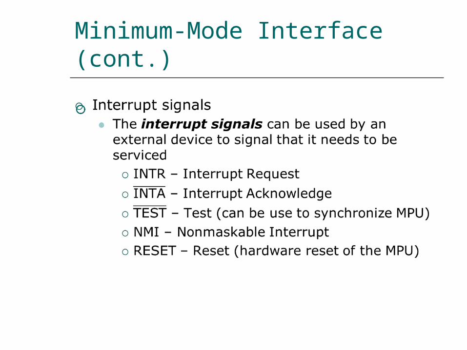
Maximum-Mode Interface (cont)
8288 bus controller
Block diagram and pin layout of 8288
Maximum-Mode Interface (cont)
8288 bus controller In the maximum-mode 80888086 outputs a
status code on three signal line S0 S1 S2 prior to the initialization of each bus cycle
The 3-bit bus status code identifies which type of bus cycle is to follow and are input to the external bus controller device 8288
The 8288 produces one or two command signals for each bus cycle
Maximum-Mode Interface (cont)
8288 bus controller
Bus status code
Maximum-Mode Interface (cont)
Maximum-Mode Interface (cont)
Maximum-Mode Interface (cont)
Queue status signals The 2-bit queue status code QS0 and QS1 tells
the external circuitry what type of information was removed form the queue during the previous clock cycle
Queue status code
Electrical Characteristics
Power is applied between pin 40 (Vcc) and pins 1 (GND) and 20 (GND)
The nominal value of Vcc is specified as +5V dc with a tolerance of plusmn10
Both 8088 and 8086 draw a maximum of 340mA from the supply
IO voltage levels
System Clock
The time base for synchronization of the internal and external operations of the microprocessor in a microcomputer system is provided by the clock (CLK) input signal The standard 8088 operates at 5 MHz and the
8088-2 operates at 8 MHz The 8086 is manufactured in three speeds 5-
MHz 8086 8-MHz 8086-2 and the 10-MHz 8086-1
The CLK is externally generated by the 8284 clock generator and driver IC
System Clock (cont)
Block diagram of the 8284 clock generator
System Clock (cont)
Block diagram of the 8284 clock generator
System Clock (cont)
Connecting the 8284 to the 8088
15- or 24MHzcrystal
Typical value of CL when used with 15MHz crystal is 12pF
The fundamental crystal frequency is divided by 3 within the 8284 to give either a 5- or 8-MHz clock signal
System Clock (cont)
CLK waveform The signal is specified at Metal Oxide
Semiconductor (MOS)-compatible voltage level The period of the 5-MHz 8088 can range from
200 ns to 500 ns and the maximum rise and fall times of its edges equal 10 ns
System Clock (cont)
PCLK and OSC signals The peripheral clock (PCLK) and oscillator clock
(OSC) signals are provided to drive peripheral ICs The clock output at PCLK is half the frequency of
CLK The OSC output is at the crystal frequency which is three times of CLK
System Clock (cont)
The 8284 can also be driven from an external clock source Applied to the EFI (External Frequency Input) Input FC is used for selection
0 crystal between X1 and X2 is used 1 selects EFI
The CSYNC input is used for external synchronization in systems with multiple clocks
System Clock (cont)
EXAMPLE If the CLK input of an 8086 MPU is to be driven by
a 9-MHz signal what speed version of the 8086 must be used and what frequency crystal must be attached to the 8284
Solution The 8086-1 is the version of the 8086 that can be
run at 9-MHz To create the 9-MHz clock a 27-MHz crystal must be used on the 8284
Bus Cycle and Time States
A bus cycle defines the basic operation that a microprocessor performs to communicate with external devices
Examples of bus cycles are the memory read memory write inputoutput read and inputoutput write
The bus cycle of the 8088 and 8086 microprocessors consists of at least four clock periods
If no bus cycles are required the microprocessor performs what are known as idle states
When READY is held at the 0 level wait states are inserted between states T3 and T4 of the bus cycle
Bus Cycle and Time States (cont)
Bus cycle clock periods idle state and wait state
Bus Cycle and Time States (cont)
EXAMPLE What is the duration of the bus cycle in the 8088-
based microcomputer if the clock is 8 MHz and the two wait states are inserted
Solution The duration of the bus cycle in an 8 MHz system
is given by tcyc = 500 ns + N x 125 ns
In this expression the N stands for the number of waits states For a bus cycle with two wait states we get
tcyc = 500 ns + 2 x 125 ns = 500 ns + 250 ns = 750 ns
Hardware Organization of the Memory Address Space
1Mx8 memory bank of the 8088
Hardware Organization of the Memory Address Space (cont)
High and low memory banks of the 8086
Hardware Organization of the Memory Address Space (cont)
Byte transfer by the 8088
Hardware Organization of the Memory Address Space (cont)
Word transfer by the 8088
Hardware Organization of the Memory Address Space (cont)
Even address byte transfer by the 8086
Hardware Organization of the Memory Address Space (cont)
Odd address byte transfer by the 8086
Hardware Organization of the Memory Address Space (cont)
Even address word transfer by the 8086
Hardware Organization of the Memory Address Space (cont)
Odd-address word transfer by the 8086
Hardware Organization of the Memory Address Space (cont)
EXAMPLE Is the word at memory address 0123116 of an
8086-based microcomputer aligned or misaligned How many cycle are required to read it from memory
Solution The first byte of the word is the second byte at
the aligned-word address 0123016 Therefore the word is misaligned and required two bus cycles to be read from memory
Address Bus Status Codes
Whenever a memory bus cycle is in progress an address bus status code S4S3 is output by the processor S4S3 identifies which one of the four segment
register is used to generate the physical address in the current bus cycle 1048729
S4S3=00 identifies the extra segment register (ES)
S4S3=01 identifies the stack segment register (SS)
S4S3=10 identifies the code segment register (CS)
S4S3=11 identifies the data segment register (DS)
The memory address reach of the microprocessor can thus be expanded to 4 Mbytes
Memory Control Signals
Minimum-mode memory control signals
Memory Control Signals (cont)
Minimum-mode memory control signals (8088) ALE ndash Address Latch Enable ndash used to latch
the address in external memory IOM ndash Input-OutputMemory ndash signal external
circuitry whether a memory of IO bus cycle is in progress
DTR ndash Data TransmitReceive ndash signal external circuitry whether the 8088 is transmitting or receiving data over the bus 1048729
RD ndash Read ndash identifies that a read bus cycle is in progress
WR ndash Write ndash identifies that a write bus cycle is in progress
DEN ndash Data Enable ndash used to enable the data bus 1048729
SSO ndash Status Line ndash identifies whether a code or data access is in progress
Memory Control Signals (cont)
The control signals for the 8086rsquos minimum-mode memory interface differs in three ways IOM signal is replaced by MIO signal The signal SSO is removed from the interface BHE (bank high enable) is added to the interface
and is used to select input for the high bank of memory in the 8086rsquos memory subsystem
Memory Control Signals (cont)
Maximum-mode memory control signals
Memory Control Signals (cont)
Maximum-mode memory control signals MRDC ndash Memory Read Command 1048729 MWTC ndash Memory Write Command 1048729 AMWC ndash Advanced Memory Write Command
Read and Write Bus Cycle
Read cycle
Minimum-mode memory read bus cycle of the 8088
Read and Write Bus Cycle (cont)
Read cycle
Minimum-mode memory read bus cycle of the 8086
Read and Write Bus Cycle (cont)
Read cycle
Maximum-mode memory read bus cycle of the 8086
Read and Write Bus Cycle (cont)
Write cycle
Minimum-mode memory write bus cycle of the 8088
Read and Write Bus Cycle (cont)
Write cycle
Maximum-mode memory write bus cycle of the 8086
Memory Interface Circuit
Address bus latches and buffers Bank write and bank read control logic Data bus transceiversbuffers Address decoders
Memory Interface Circuit (cont)
Memory interface block diagram
Memory Interface Circuit (cont)
Address bus latches and buffers
Block diagram of a D-type latch
Memory Interface Circuit (cont)
Address bus latches and buffers
Circuit diagram of the 74F373
Memory Interface Circuit (cont)
A review of flip-floplatch logic
Positive edge-triggered D flip-flop
Memory Interface Circuit (cont)
A review of flip-floplatch logic
Positive edge-triggered JK flip-flop
Memory Interface Circuit (cont)
A review of flip-floplatch logic
D-type latch
Memory Interface Circuit (cont)
Address bus latches and buffers
Address latch circuit
Memory Interface Circuit (cont)
Bank write and bank read control logic
Bank write control logic Bank read control logic
Memory Interface Circuit (cont)
Data bus transceivers
Block diagram and circuit diagram of the 74F245 octal bus transceiver
Memory Interface Circuit (cont)
Data bus transceivers
Data bus transceiver circuit
Memory Interface Circuit (cont)
Address decoder
Address bus configuration with address decoding
Memory Interface Circuit (cont)
Address decoder
Block diagram and operation of the 74F139 decoder
Memory Interface Circuit (cont)
Address decoder
Circuit diagram of the 74F139 decoder
Memory Interface Circuit (cont)
Address decoder
Address decoder circuit using 74F139
Memory Interface Circuit (cont)
Address decoder
Block diagram and operation of the 74F138 decoder
Memory Interface Circuit (cont)
Address decoder
Circuit diagram of the 74F138 decoder
Memory Interface Circuit (cont)
Address decoder
Address decoder circuit using 74F138
Types of InputOutput
The IO system allows peripherals to provide data or receive results of processing the data Using IO ports
The 80888086 MPU can employ two types of IO Isolated IO Memory-mapped IO
They differ in how IO ports are mapped into the address space
Types of InputOutput (cont)
Isolated inputoutput When using isolated IO in a microcomputer
system the IO device are treated separate from memory
The memory address space contains 1 M consecutive byte address in the range 0000016 through FFFFF16
The IO address space contains 64K consecutive byte addresses in the range 000016 through FFFF16
The bytes in two consecutive IO addresses can be accessed as word-wide data
Page 0 000016 00FF16
Certain IO instructions can only perform in this range
Types of InputOutput (cont)
Isolated inputoutput
80888086 memory and IO address spaces
Types of InputOutput (cont)
Isolated inputoutput
Isolated IO ports
Types of InputOutput (cont)
Isolated inputoutput Advantages
The complete 1Mbyte memory address space is available for use with memory
Special instructions have been provided to perform IO operations with maximized performance
The bytes in two consecutive IO addresses can be accessed as word-wide data
Disadvantages All input and output data transfers must take place
between the AL or AX register and IO port
Types of InputOutput (cont)
Memory-mapped inputoutput MPU looks at the IO port as though it is a storage
location in memory Some of the memory address space is dedicated to IO
ports Instructions that affect data in memory are used
instead of the special IO instructions More instructions and addressing modes are available to
perform IO operations IO transfers can take place between IO port and other
internal registers The memory instructions tend to execute slower
than those specifically designed for isolated IO Part of the memory address space is lost
Types of InputOutput(cont)
Memory-mapped inputoutput
Memory mapped IO ports
Isolated InputOutput Interface
IO devices Keyboard Printer Mouse 82C55A etc
Functions of interface circuit Select the IO port Latch output data Sample input data Synchronize data transfer Translate between TTL voltage levels and those
required to operate the IO devices
Isolated InputOutput Interface (cont)
Minimum-mode interface
Minimum-mode 8088 system IO interface
Isolated InputOutput Interface (cont)
Minimum-mode interface
Minimum-mode 8086 system IO interface
Isolated InputOutput Interface (cont)
Maximum-mode interface
Maximum-mode 8088 system IO interface
Isolated InputOutput Interface (cont)
Maximum-mode interface
Maximum-mode 8086 system IO interface
Isolated InputOutput Interface (cont)
Maximum-mode interface
IO bus cycle status codes
InputOutput Data Transfer
Inputoutput data transfers in the 8088 and 8086 microcomputers can be either byte-wide or word-wide
IO addresses are 16 bits in length and are output by the 8088 to the IO interface over bus lines AD0 through AD7 and A8 through A15
In 8088 the word transfers is performed as two consecutive byte-wide data transfer and takes two bus cycle
In 8086 the word transfers can takes either one or two bus cycle
Word-wide IO ports should be aligned at even-address boundaries
InputOutput Data Instructions
InputOutput Data Instructions(cont)
EXAMPLE Write a sequence of instructions that will output
the data FF16 to a byte-wide output port at address AB16 of the IO address space
Solution First the AL register is loaded with FF16 as an
immediate operand in the instruction
MOV AL 0FFH Now the data in AL can be output to the byte-
wide output port with the instruction
OUT 0ABH AL
InputOutput Data Instructions(cont)
EXAMPLE Write a series of instructions that will output FF16 to an
output port located at address B00016 of the IO address space
Solution The DX register must first be loaded with the address
of the output port This is done with the instructionMOV DX 0B000H
Next the data that are to be output must be loaded into AL with the instruction
MOV AL 0FFH Finally the data are output with the instruction
OUT DX AL
InputOutput Data Instructions(cont)
EXAMPLE Data are to be read in from two byte-wide input
ports at addresses AA16 and A916 and then output as a word-wide output port at address B00016 Write a sequence of instructions to perform this inputoutput operation
InputOutput Data Instructions(cont)
Solution First read in the byte at address AA16 into AL and
move it into AHIN AL 0AAHMOV AH AL
Now the other byte can be read into AL by the instructionIN AL 09AH
And to write out the word of dataMOV DX 0B000HOUT DX AX
InputOutput Bus Cycles
Input bus cycle of the 8088
InputOutput Bus Cycles (cont)
Output bus cycle of the 8088
InputOutput Bus Cycles (cont)
Input bus cycle of the 8086
InputOutput Bus Cycles (cont)
Output bus cycle of the 8086
Maximum-Mode Interface (cont)
8288 bus controller
Bus status code
Maximum-Mode Interface (cont)
Maximum-Mode Interface (cont)
Maximum-Mode Interface (cont)
Queue status signals The 2-bit queue status code QS0 and QS1 tells
the external circuitry what type of information was removed form the queue during the previous clock cycle
Queue status code
Electrical Characteristics
Power is applied between pin 40 (Vcc) and pins 1 (GND) and 20 (GND)
The nominal value of Vcc is specified as +5V dc with a tolerance of plusmn10
Both 8088 and 8086 draw a maximum of 340mA from the supply
IO voltage levels
System Clock
The time base for synchronization of the internal and external operations of the microprocessor in a microcomputer system is provided by the clock (CLK) input signal The standard 8088 operates at 5 MHz and the
8088-2 operates at 8 MHz The 8086 is manufactured in three speeds 5-
MHz 8086 8-MHz 8086-2 and the 10-MHz 8086-1
The CLK is externally generated by the 8284 clock generator and driver IC
System Clock (cont)
Block diagram of the 8284 clock generator
System Clock (cont)
Block diagram of the 8284 clock generator
System Clock (cont)
Connecting the 8284 to the 8088
15- or 24MHzcrystal
Typical value of CL when used with 15MHz crystal is 12pF
The fundamental crystal frequency is divided by 3 within the 8284 to give either a 5- or 8-MHz clock signal
System Clock (cont)
CLK waveform The signal is specified at Metal Oxide
Semiconductor (MOS)-compatible voltage level The period of the 5-MHz 8088 can range from
200 ns to 500 ns and the maximum rise and fall times of its edges equal 10 ns
System Clock (cont)
PCLK and OSC signals The peripheral clock (PCLK) and oscillator clock
(OSC) signals are provided to drive peripheral ICs The clock output at PCLK is half the frequency of
CLK The OSC output is at the crystal frequency which is three times of CLK
System Clock (cont)
The 8284 can also be driven from an external clock source Applied to the EFI (External Frequency Input) Input FC is used for selection
0 crystal between X1 and X2 is used 1 selects EFI
The CSYNC input is used for external synchronization in systems with multiple clocks
System Clock (cont)
EXAMPLE If the CLK input of an 8086 MPU is to be driven by
a 9-MHz signal what speed version of the 8086 must be used and what frequency crystal must be attached to the 8284
Solution The 8086-1 is the version of the 8086 that can be
run at 9-MHz To create the 9-MHz clock a 27-MHz crystal must be used on the 8284
Bus Cycle and Time States
A bus cycle defines the basic operation that a microprocessor performs to communicate with external devices
Examples of bus cycles are the memory read memory write inputoutput read and inputoutput write
The bus cycle of the 8088 and 8086 microprocessors consists of at least four clock periods
If no bus cycles are required the microprocessor performs what are known as idle states
When READY is held at the 0 level wait states are inserted between states T3 and T4 of the bus cycle
Bus Cycle and Time States (cont)
Bus cycle clock periods idle state and wait state
Bus Cycle and Time States (cont)
EXAMPLE What is the duration of the bus cycle in the 8088-
based microcomputer if the clock is 8 MHz and the two wait states are inserted
Solution The duration of the bus cycle in an 8 MHz system
is given by tcyc = 500 ns + N x 125 ns
In this expression the N stands for the number of waits states For a bus cycle with two wait states we get
tcyc = 500 ns + 2 x 125 ns = 500 ns + 250 ns = 750 ns
Hardware Organization of the Memory Address Space
1Mx8 memory bank of the 8088
Hardware Organization of the Memory Address Space (cont)
High and low memory banks of the 8086
Hardware Organization of the Memory Address Space (cont)
Byte transfer by the 8088
Hardware Organization of the Memory Address Space (cont)
Word transfer by the 8088
Hardware Organization of the Memory Address Space (cont)
Even address byte transfer by the 8086
Hardware Organization of the Memory Address Space (cont)
Odd address byte transfer by the 8086
Hardware Organization of the Memory Address Space (cont)
Even address word transfer by the 8086
Hardware Organization of the Memory Address Space (cont)
Odd-address word transfer by the 8086
Hardware Organization of the Memory Address Space (cont)
EXAMPLE Is the word at memory address 0123116 of an
8086-based microcomputer aligned or misaligned How many cycle are required to read it from memory
Solution The first byte of the word is the second byte at
the aligned-word address 0123016 Therefore the word is misaligned and required two bus cycles to be read from memory
Address Bus Status Codes
Whenever a memory bus cycle is in progress an address bus status code S4S3 is output by the processor S4S3 identifies which one of the four segment
register is used to generate the physical address in the current bus cycle 1048729
S4S3=00 identifies the extra segment register (ES)
S4S3=01 identifies the stack segment register (SS)
S4S3=10 identifies the code segment register (CS)
S4S3=11 identifies the data segment register (DS)
The memory address reach of the microprocessor can thus be expanded to 4 Mbytes
Memory Control Signals
Minimum-mode memory control signals
Memory Control Signals (cont)
Minimum-mode memory control signals (8088) ALE ndash Address Latch Enable ndash used to latch
the address in external memory IOM ndash Input-OutputMemory ndash signal external
circuitry whether a memory of IO bus cycle is in progress
DTR ndash Data TransmitReceive ndash signal external circuitry whether the 8088 is transmitting or receiving data over the bus 1048729
RD ndash Read ndash identifies that a read bus cycle is in progress
WR ndash Write ndash identifies that a write bus cycle is in progress
DEN ndash Data Enable ndash used to enable the data bus 1048729
SSO ndash Status Line ndash identifies whether a code or data access is in progress
Memory Control Signals (cont)
The control signals for the 8086rsquos minimum-mode memory interface differs in three ways IOM signal is replaced by MIO signal The signal SSO is removed from the interface BHE (bank high enable) is added to the interface
and is used to select input for the high bank of memory in the 8086rsquos memory subsystem
Memory Control Signals (cont)
Maximum-mode memory control signals
Memory Control Signals (cont)
Maximum-mode memory control signals MRDC ndash Memory Read Command 1048729 MWTC ndash Memory Write Command 1048729 AMWC ndash Advanced Memory Write Command
Read and Write Bus Cycle
Read cycle
Minimum-mode memory read bus cycle of the 8088
Read and Write Bus Cycle (cont)
Read cycle
Minimum-mode memory read bus cycle of the 8086
Read and Write Bus Cycle (cont)
Read cycle
Maximum-mode memory read bus cycle of the 8086
Read and Write Bus Cycle (cont)
Write cycle
Minimum-mode memory write bus cycle of the 8088
Read and Write Bus Cycle (cont)
Write cycle
Maximum-mode memory write bus cycle of the 8086
Memory Interface Circuit
Address bus latches and buffers Bank write and bank read control logic Data bus transceiversbuffers Address decoders
Memory Interface Circuit (cont)
Memory interface block diagram
Memory Interface Circuit (cont)
Address bus latches and buffers
Block diagram of a D-type latch
Memory Interface Circuit (cont)
Address bus latches and buffers
Circuit diagram of the 74F373
Memory Interface Circuit (cont)
A review of flip-floplatch logic
Positive edge-triggered D flip-flop
Memory Interface Circuit (cont)
A review of flip-floplatch logic
Positive edge-triggered JK flip-flop
Memory Interface Circuit (cont)
A review of flip-floplatch logic
D-type latch
Memory Interface Circuit (cont)
Address bus latches and buffers
Address latch circuit
Memory Interface Circuit (cont)
Bank write and bank read control logic
Bank write control logic Bank read control logic
Memory Interface Circuit (cont)
Data bus transceivers
Block diagram and circuit diagram of the 74F245 octal bus transceiver
Memory Interface Circuit (cont)
Data bus transceivers
Data bus transceiver circuit
Memory Interface Circuit (cont)
Address decoder
Address bus configuration with address decoding
Memory Interface Circuit (cont)
Address decoder
Block diagram and operation of the 74F139 decoder
Memory Interface Circuit (cont)
Address decoder
Circuit diagram of the 74F139 decoder
Memory Interface Circuit (cont)
Address decoder
Address decoder circuit using 74F139
Memory Interface Circuit (cont)
Address decoder
Block diagram and operation of the 74F138 decoder
Memory Interface Circuit (cont)
Address decoder
Circuit diagram of the 74F138 decoder
Memory Interface Circuit (cont)
Address decoder
Address decoder circuit using 74F138
Types of InputOutput
The IO system allows peripherals to provide data or receive results of processing the data Using IO ports
The 80888086 MPU can employ two types of IO Isolated IO Memory-mapped IO
They differ in how IO ports are mapped into the address space
Types of InputOutput (cont)
Isolated inputoutput When using isolated IO in a microcomputer
system the IO device are treated separate from memory
The memory address space contains 1 M consecutive byte address in the range 0000016 through FFFFF16
The IO address space contains 64K consecutive byte addresses in the range 000016 through FFFF16
The bytes in two consecutive IO addresses can be accessed as word-wide data
Page 0 000016 00FF16
Certain IO instructions can only perform in this range
Types of InputOutput (cont)
Isolated inputoutput
80888086 memory and IO address spaces
Types of InputOutput (cont)
Isolated inputoutput
Isolated IO ports
Types of InputOutput (cont)
Isolated inputoutput Advantages
The complete 1Mbyte memory address space is available for use with memory
Special instructions have been provided to perform IO operations with maximized performance
The bytes in two consecutive IO addresses can be accessed as word-wide data
Disadvantages All input and output data transfers must take place
between the AL or AX register and IO port
Types of InputOutput (cont)
Memory-mapped inputoutput MPU looks at the IO port as though it is a storage
location in memory Some of the memory address space is dedicated to IO
ports Instructions that affect data in memory are used
instead of the special IO instructions More instructions and addressing modes are available to
perform IO operations IO transfers can take place between IO port and other
internal registers The memory instructions tend to execute slower
than those specifically designed for isolated IO Part of the memory address space is lost
Types of InputOutput(cont)
Memory-mapped inputoutput
Memory mapped IO ports
Isolated InputOutput Interface
IO devices Keyboard Printer Mouse 82C55A etc
Functions of interface circuit Select the IO port Latch output data Sample input data Synchronize data transfer Translate between TTL voltage levels and those
required to operate the IO devices
Isolated InputOutput Interface (cont)
Minimum-mode interface
Minimum-mode 8088 system IO interface
Isolated InputOutput Interface (cont)
Minimum-mode interface
Minimum-mode 8086 system IO interface
Isolated InputOutput Interface (cont)
Maximum-mode interface
Maximum-mode 8088 system IO interface
Isolated InputOutput Interface (cont)
Maximum-mode interface
Maximum-mode 8086 system IO interface
Isolated InputOutput Interface (cont)
Maximum-mode interface
IO bus cycle status codes
InputOutput Data Transfer
Inputoutput data transfers in the 8088 and 8086 microcomputers can be either byte-wide or word-wide
IO addresses are 16 bits in length and are output by the 8088 to the IO interface over bus lines AD0 through AD7 and A8 through A15
In 8088 the word transfers is performed as two consecutive byte-wide data transfer and takes two bus cycle
In 8086 the word transfers can takes either one or two bus cycle
Word-wide IO ports should be aligned at even-address boundaries
InputOutput Data Instructions
InputOutput Data Instructions(cont)
EXAMPLE Write a sequence of instructions that will output
the data FF16 to a byte-wide output port at address AB16 of the IO address space
Solution First the AL register is loaded with FF16 as an
immediate operand in the instruction
MOV AL 0FFH Now the data in AL can be output to the byte-
wide output port with the instruction
OUT 0ABH AL
InputOutput Data Instructions(cont)
EXAMPLE Write a series of instructions that will output FF16 to an
output port located at address B00016 of the IO address space
Solution The DX register must first be loaded with the address
of the output port This is done with the instructionMOV DX 0B000H
Next the data that are to be output must be loaded into AL with the instruction
MOV AL 0FFH Finally the data are output with the instruction
OUT DX AL
InputOutput Data Instructions(cont)
EXAMPLE Data are to be read in from two byte-wide input
ports at addresses AA16 and A916 and then output as a word-wide output port at address B00016 Write a sequence of instructions to perform this inputoutput operation
InputOutput Data Instructions(cont)
Solution First read in the byte at address AA16 into AL and
move it into AHIN AL 0AAHMOV AH AL
Now the other byte can be read into AL by the instructionIN AL 09AH
And to write out the word of dataMOV DX 0B000HOUT DX AX
InputOutput Bus Cycles
Input bus cycle of the 8088
InputOutput Bus Cycles (cont)
Output bus cycle of the 8088
InputOutput Bus Cycles (cont)
Input bus cycle of the 8086
InputOutput Bus Cycles (cont)
Output bus cycle of the 8086

Maximum-Mode Interface (cont)
Maximum-Mode Interface (cont)
Maximum-Mode Interface (cont)
Queue status signals The 2-bit queue status code QS0 and QS1 tells
the external circuitry what type of information was removed form the queue during the previous clock cycle
Queue status code
Electrical Characteristics
Power is applied between pin 40 (Vcc) and pins 1 (GND) and 20 (GND)
The nominal value of Vcc is specified as +5V dc with a tolerance of plusmn10
Both 8088 and 8086 draw a maximum of 340mA from the supply
IO voltage levels
System Clock
The time base for synchronization of the internal and external operations of the microprocessor in a microcomputer system is provided by the clock (CLK) input signal The standard 8088 operates at 5 MHz and the
8088-2 operates at 8 MHz The 8086 is manufactured in three speeds 5-
MHz 8086 8-MHz 8086-2 and the 10-MHz 8086-1
The CLK is externally generated by the 8284 clock generator and driver IC
System Clock (cont)
Block diagram of the 8284 clock generator
System Clock (cont)
Block diagram of the 8284 clock generator
System Clock (cont)
Connecting the 8284 to the 8088
15- or 24MHzcrystal
Typical value of CL when used with 15MHz crystal is 12pF
The fundamental crystal frequency is divided by 3 within the 8284 to give either a 5- or 8-MHz clock signal
System Clock (cont)
CLK waveform The signal is specified at Metal Oxide
Semiconductor (MOS)-compatible voltage level The period of the 5-MHz 8088 can range from
200 ns to 500 ns and the maximum rise and fall times of its edges equal 10 ns
System Clock (cont)
PCLK and OSC signals The peripheral clock (PCLK) and oscillator clock
(OSC) signals are provided to drive peripheral ICs The clock output at PCLK is half the frequency of
CLK The OSC output is at the crystal frequency which is three times of CLK
System Clock (cont)
The 8284 can also be driven from an external clock source Applied to the EFI (External Frequency Input) Input FC is used for selection
0 crystal between X1 and X2 is used 1 selects EFI
The CSYNC input is used for external synchronization in systems with multiple clocks
System Clock (cont)
EXAMPLE If the CLK input of an 8086 MPU is to be driven by
a 9-MHz signal what speed version of the 8086 must be used and what frequency crystal must be attached to the 8284
Solution The 8086-1 is the version of the 8086 that can be
run at 9-MHz To create the 9-MHz clock a 27-MHz crystal must be used on the 8284
Bus Cycle and Time States
A bus cycle defines the basic operation that a microprocessor performs to communicate with external devices
Examples of bus cycles are the memory read memory write inputoutput read and inputoutput write
The bus cycle of the 8088 and 8086 microprocessors consists of at least four clock periods
If no bus cycles are required the microprocessor performs what are known as idle states
When READY is held at the 0 level wait states are inserted between states T3 and T4 of the bus cycle
Bus Cycle and Time States (cont)
Bus cycle clock periods idle state and wait state
Bus Cycle and Time States (cont)
EXAMPLE What is the duration of the bus cycle in the 8088-
based microcomputer if the clock is 8 MHz and the two wait states are inserted
Solution The duration of the bus cycle in an 8 MHz system
is given by tcyc = 500 ns + N x 125 ns
In this expression the N stands for the number of waits states For a bus cycle with two wait states we get
tcyc = 500 ns + 2 x 125 ns = 500 ns + 250 ns = 750 ns
Hardware Organization of the Memory Address Space
1Mx8 memory bank of the 8088
Hardware Organization of the Memory Address Space (cont)
High and low memory banks of the 8086
Hardware Organization of the Memory Address Space (cont)
Byte transfer by the 8088
Hardware Organization of the Memory Address Space (cont)
Word transfer by the 8088
Hardware Organization of the Memory Address Space (cont)
Even address byte transfer by the 8086
Hardware Organization of the Memory Address Space (cont)
Odd address byte transfer by the 8086
Hardware Organization of the Memory Address Space (cont)
Even address word transfer by the 8086
Hardware Organization of the Memory Address Space (cont)
Odd-address word transfer by the 8086
Hardware Organization of the Memory Address Space (cont)
EXAMPLE Is the word at memory address 0123116 of an
8086-based microcomputer aligned or misaligned How many cycle are required to read it from memory
Solution The first byte of the word is the second byte at
the aligned-word address 0123016 Therefore the word is misaligned and required two bus cycles to be read from memory
Address Bus Status Codes
Whenever a memory bus cycle is in progress an address bus status code S4S3 is output by the processor S4S3 identifies which one of the four segment
register is used to generate the physical address in the current bus cycle 1048729
S4S3=00 identifies the extra segment register (ES)
S4S3=01 identifies the stack segment register (SS)
S4S3=10 identifies the code segment register (CS)
S4S3=11 identifies the data segment register (DS)
The memory address reach of the microprocessor can thus be expanded to 4 Mbytes
Memory Control Signals
Minimum-mode memory control signals
Memory Control Signals (cont)
Minimum-mode memory control signals (8088) ALE ndash Address Latch Enable ndash used to latch
the address in external memory IOM ndash Input-OutputMemory ndash signal external
circuitry whether a memory of IO bus cycle is in progress
DTR ndash Data TransmitReceive ndash signal external circuitry whether the 8088 is transmitting or receiving data over the bus 1048729
RD ndash Read ndash identifies that a read bus cycle is in progress
WR ndash Write ndash identifies that a write bus cycle is in progress
DEN ndash Data Enable ndash used to enable the data bus 1048729
SSO ndash Status Line ndash identifies whether a code or data access is in progress
Memory Control Signals (cont)
The control signals for the 8086rsquos minimum-mode memory interface differs in three ways IOM signal is replaced by MIO signal The signal SSO is removed from the interface BHE (bank high enable) is added to the interface
and is used to select input for the high bank of memory in the 8086rsquos memory subsystem
Memory Control Signals (cont)
Maximum-mode memory control signals
Memory Control Signals (cont)
Maximum-mode memory control signals MRDC ndash Memory Read Command 1048729 MWTC ndash Memory Write Command 1048729 AMWC ndash Advanced Memory Write Command
Read and Write Bus Cycle
Read cycle
Minimum-mode memory read bus cycle of the 8088
Read and Write Bus Cycle (cont)
Read cycle
Minimum-mode memory read bus cycle of the 8086
Read and Write Bus Cycle (cont)
Read cycle
Maximum-mode memory read bus cycle of the 8086
Read and Write Bus Cycle (cont)
Write cycle
Minimum-mode memory write bus cycle of the 8088
Read and Write Bus Cycle (cont)
Write cycle
Maximum-mode memory write bus cycle of the 8086
Memory Interface Circuit
Address bus latches and buffers Bank write and bank read control logic Data bus transceiversbuffers Address decoders
Memory Interface Circuit (cont)
Memory interface block diagram
Memory Interface Circuit (cont)
Address bus latches and buffers
Block diagram of a D-type latch
Memory Interface Circuit (cont)
Address bus latches and buffers
Circuit diagram of the 74F373
Memory Interface Circuit (cont)
A review of flip-floplatch logic
Positive edge-triggered D flip-flop
Memory Interface Circuit (cont)
A review of flip-floplatch logic
Positive edge-triggered JK flip-flop
Memory Interface Circuit (cont)
A review of flip-floplatch logic
D-type latch
Memory Interface Circuit (cont)
Address bus latches and buffers
Address latch circuit
Memory Interface Circuit (cont)
Bank write and bank read control logic
Bank write control logic Bank read control logic
Memory Interface Circuit (cont)
Data bus transceivers
Block diagram and circuit diagram of the 74F245 octal bus transceiver
Memory Interface Circuit (cont)
Data bus transceivers
Data bus transceiver circuit
Memory Interface Circuit (cont)
Address decoder
Address bus configuration with address decoding
Memory Interface Circuit (cont)
Address decoder
Block diagram and operation of the 74F139 decoder
Memory Interface Circuit (cont)
Address decoder
Circuit diagram of the 74F139 decoder
Memory Interface Circuit (cont)
Address decoder
Address decoder circuit using 74F139
Memory Interface Circuit (cont)
Address decoder
Block diagram and operation of the 74F138 decoder
Memory Interface Circuit (cont)
Address decoder
Circuit diagram of the 74F138 decoder
Memory Interface Circuit (cont)
Address decoder
Address decoder circuit using 74F138
Types of InputOutput
The IO system allows peripherals to provide data or receive results of processing the data Using IO ports
The 80888086 MPU can employ two types of IO Isolated IO Memory-mapped IO
They differ in how IO ports are mapped into the address space
Types of InputOutput (cont)
Isolated inputoutput When using isolated IO in a microcomputer
system the IO device are treated separate from memory
The memory address space contains 1 M consecutive byte address in the range 0000016 through FFFFF16
The IO address space contains 64K consecutive byte addresses in the range 000016 through FFFF16
The bytes in two consecutive IO addresses can be accessed as word-wide data
Page 0 000016 00FF16
Certain IO instructions can only perform in this range
Types of InputOutput (cont)
Isolated inputoutput
80888086 memory and IO address spaces
Types of InputOutput (cont)
Isolated inputoutput
Isolated IO ports
Types of InputOutput (cont)
Isolated inputoutput Advantages
The complete 1Mbyte memory address space is available for use with memory
Special instructions have been provided to perform IO operations with maximized performance
The bytes in two consecutive IO addresses can be accessed as word-wide data
Disadvantages All input and output data transfers must take place
between the AL or AX register and IO port
Types of InputOutput (cont)
Memory-mapped inputoutput MPU looks at the IO port as though it is a storage
location in memory Some of the memory address space is dedicated to IO
ports Instructions that affect data in memory are used
instead of the special IO instructions More instructions and addressing modes are available to
perform IO operations IO transfers can take place between IO port and other
internal registers The memory instructions tend to execute slower
than those specifically designed for isolated IO Part of the memory address space is lost
Types of InputOutput(cont)
Memory-mapped inputoutput
Memory mapped IO ports
Isolated InputOutput Interface
IO devices Keyboard Printer Mouse 82C55A etc
Functions of interface circuit Select the IO port Latch output data Sample input data Synchronize data transfer Translate between TTL voltage levels and those
required to operate the IO devices
Isolated InputOutput Interface (cont)
Minimum-mode interface
Minimum-mode 8088 system IO interface
Isolated InputOutput Interface (cont)
Minimum-mode interface
Minimum-mode 8086 system IO interface
Isolated InputOutput Interface (cont)
Maximum-mode interface
Maximum-mode 8088 system IO interface
Isolated InputOutput Interface (cont)
Maximum-mode interface
Maximum-mode 8086 system IO interface
Isolated InputOutput Interface (cont)
Maximum-mode interface
IO bus cycle status codes
InputOutput Data Transfer
Inputoutput data transfers in the 8088 and 8086 microcomputers can be either byte-wide or word-wide
IO addresses are 16 bits in length and are output by the 8088 to the IO interface over bus lines AD0 through AD7 and A8 through A15
In 8088 the word transfers is performed as two consecutive byte-wide data transfer and takes two bus cycle
In 8086 the word transfers can takes either one or two bus cycle
Word-wide IO ports should be aligned at even-address boundaries
InputOutput Data Instructions
InputOutput Data Instructions(cont)
EXAMPLE Write a sequence of instructions that will output
the data FF16 to a byte-wide output port at address AB16 of the IO address space
Solution First the AL register is loaded with FF16 as an
immediate operand in the instruction
MOV AL 0FFH Now the data in AL can be output to the byte-
wide output port with the instruction
OUT 0ABH AL
InputOutput Data Instructions(cont)
EXAMPLE Write a series of instructions that will output FF16 to an
output port located at address B00016 of the IO address space
Solution The DX register must first be loaded with the address
of the output port This is done with the instructionMOV DX 0B000H
Next the data that are to be output must be loaded into AL with the instruction
MOV AL 0FFH Finally the data are output with the instruction
OUT DX AL
InputOutput Data Instructions(cont)
EXAMPLE Data are to be read in from two byte-wide input
ports at addresses AA16 and A916 and then output as a word-wide output port at address B00016 Write a sequence of instructions to perform this inputoutput operation
InputOutput Data Instructions(cont)
Solution First read in the byte at address AA16 into AL and
move it into AHIN AL 0AAHMOV AH AL
Now the other byte can be read into AL by the instructionIN AL 09AH
And to write out the word of dataMOV DX 0B000HOUT DX AX
InputOutput Bus Cycles
Input bus cycle of the 8088
InputOutput Bus Cycles (cont)
Output bus cycle of the 8088
InputOutput Bus Cycles (cont)
Input bus cycle of the 8086
InputOutput Bus Cycles (cont)
Output bus cycle of the 8086
Maximum-Mode Interface (cont)
Maximum-Mode Interface (cont)
Queue status signals The 2-bit queue status code QS0 and QS1 tells
the external circuitry what type of information was removed form the queue during the previous clock cycle
Queue status code
Electrical Characteristics
Power is applied between pin 40 (Vcc) and pins 1 (GND) and 20 (GND)
The nominal value of Vcc is specified as +5V dc with a tolerance of plusmn10
Both 8088 and 8086 draw a maximum of 340mA from the supply
IO voltage levels
System Clock
The time base for synchronization of the internal and external operations of the microprocessor in a microcomputer system is provided by the clock (CLK) input signal The standard 8088 operates at 5 MHz and the
8088-2 operates at 8 MHz The 8086 is manufactured in three speeds 5-
MHz 8086 8-MHz 8086-2 and the 10-MHz 8086-1
The CLK is externally generated by the 8284 clock generator and driver IC
System Clock (cont)
Block diagram of the 8284 clock generator
System Clock (cont)
Block diagram of the 8284 clock generator
System Clock (cont)
Connecting the 8284 to the 8088
15- or 24MHzcrystal
Typical value of CL when used with 15MHz crystal is 12pF
The fundamental crystal frequency is divided by 3 within the 8284 to give either a 5- or 8-MHz clock signal
System Clock (cont)
CLK waveform The signal is specified at Metal Oxide
Semiconductor (MOS)-compatible voltage level The period of the 5-MHz 8088 can range from
200 ns to 500 ns and the maximum rise and fall times of its edges equal 10 ns
System Clock (cont)
PCLK and OSC signals The peripheral clock (PCLK) and oscillator clock
(OSC) signals are provided to drive peripheral ICs The clock output at PCLK is half the frequency of
CLK The OSC output is at the crystal frequency which is three times of CLK
System Clock (cont)
The 8284 can also be driven from an external clock source Applied to the EFI (External Frequency Input) Input FC is used for selection
0 crystal between X1 and X2 is used 1 selects EFI
The CSYNC input is used for external synchronization in systems with multiple clocks
System Clock (cont)
EXAMPLE If the CLK input of an 8086 MPU is to be driven by
a 9-MHz signal what speed version of the 8086 must be used and what frequency crystal must be attached to the 8284
Solution The 8086-1 is the version of the 8086 that can be
run at 9-MHz To create the 9-MHz clock a 27-MHz crystal must be used on the 8284
Bus Cycle and Time States
A bus cycle defines the basic operation that a microprocessor performs to communicate with external devices
Examples of bus cycles are the memory read memory write inputoutput read and inputoutput write
The bus cycle of the 8088 and 8086 microprocessors consists of at least four clock periods
If no bus cycles are required the microprocessor performs what are known as idle states
When READY is held at the 0 level wait states are inserted between states T3 and T4 of the bus cycle
Bus Cycle and Time States (cont)
Bus cycle clock periods idle state and wait state
Bus Cycle and Time States (cont)
EXAMPLE What is the duration of the bus cycle in the 8088-
based microcomputer if the clock is 8 MHz and the two wait states are inserted
Solution The duration of the bus cycle in an 8 MHz system
is given by tcyc = 500 ns + N x 125 ns
In this expression the N stands for the number of waits states For a bus cycle with two wait states we get
tcyc = 500 ns + 2 x 125 ns = 500 ns + 250 ns = 750 ns
Hardware Organization of the Memory Address Space
1Mx8 memory bank of the 8088
Hardware Organization of the Memory Address Space (cont)
High and low memory banks of the 8086
Hardware Organization of the Memory Address Space (cont)
Byte transfer by the 8088
Hardware Organization of the Memory Address Space (cont)
Word transfer by the 8088
Hardware Organization of the Memory Address Space (cont)
Even address byte transfer by the 8086
Hardware Organization of the Memory Address Space (cont)
Odd address byte transfer by the 8086
Hardware Organization of the Memory Address Space (cont)
Even address word transfer by the 8086
Hardware Organization of the Memory Address Space (cont)
Odd-address word transfer by the 8086
Hardware Organization of the Memory Address Space (cont)
EXAMPLE Is the word at memory address 0123116 of an
8086-based microcomputer aligned or misaligned How many cycle are required to read it from memory
Solution The first byte of the word is the second byte at
the aligned-word address 0123016 Therefore the word is misaligned and required two bus cycles to be read from memory
Address Bus Status Codes
Whenever a memory bus cycle is in progress an address bus status code S4S3 is output by the processor S4S3 identifies which one of the four segment
register is used to generate the physical address in the current bus cycle 1048729
S4S3=00 identifies the extra segment register (ES)
S4S3=01 identifies the stack segment register (SS)
S4S3=10 identifies the code segment register (CS)
S4S3=11 identifies the data segment register (DS)
The memory address reach of the microprocessor can thus be expanded to 4 Mbytes
Memory Control Signals
Minimum-mode memory control signals
Memory Control Signals (cont)
Minimum-mode memory control signals (8088) ALE ndash Address Latch Enable ndash used to latch
the address in external memory IOM ndash Input-OutputMemory ndash signal external
circuitry whether a memory of IO bus cycle is in progress
DTR ndash Data TransmitReceive ndash signal external circuitry whether the 8088 is transmitting or receiving data over the bus 1048729
RD ndash Read ndash identifies that a read bus cycle is in progress
WR ndash Write ndash identifies that a write bus cycle is in progress
DEN ndash Data Enable ndash used to enable the data bus 1048729
SSO ndash Status Line ndash identifies whether a code or data access is in progress
Memory Control Signals (cont)
The control signals for the 8086rsquos minimum-mode memory interface differs in three ways IOM signal is replaced by MIO signal The signal SSO is removed from the interface BHE (bank high enable) is added to the interface
and is used to select input for the high bank of memory in the 8086rsquos memory subsystem
Memory Control Signals (cont)
Maximum-mode memory control signals
Memory Control Signals (cont)
Maximum-mode memory control signals MRDC ndash Memory Read Command 1048729 MWTC ndash Memory Write Command 1048729 AMWC ndash Advanced Memory Write Command
Read and Write Bus Cycle
Read cycle
Minimum-mode memory read bus cycle of the 8088
Read and Write Bus Cycle (cont)
Read cycle
Minimum-mode memory read bus cycle of the 8086
Read and Write Bus Cycle (cont)
Read cycle
Maximum-mode memory read bus cycle of the 8086
Read and Write Bus Cycle (cont)
Write cycle
Minimum-mode memory write bus cycle of the 8088
Read and Write Bus Cycle (cont)
Write cycle
Maximum-mode memory write bus cycle of the 8086
Memory Interface Circuit
Address bus latches and buffers Bank write and bank read control logic Data bus transceiversbuffers Address decoders
Memory Interface Circuit (cont)
Memory interface block diagram
Memory Interface Circuit (cont)
Address bus latches and buffers
Block diagram of a D-type latch
Memory Interface Circuit (cont)
Address bus latches and buffers
Circuit diagram of the 74F373
Memory Interface Circuit (cont)
A review of flip-floplatch logic
Positive edge-triggered D flip-flop
Memory Interface Circuit (cont)
A review of flip-floplatch logic
Positive edge-triggered JK flip-flop
Memory Interface Circuit (cont)
A review of flip-floplatch logic
D-type latch
Memory Interface Circuit (cont)
Address bus latches and buffers
Address latch circuit
Memory Interface Circuit (cont)
Bank write and bank read control logic
Bank write control logic Bank read control logic
Memory Interface Circuit (cont)
Data bus transceivers
Block diagram and circuit diagram of the 74F245 octal bus transceiver
Memory Interface Circuit (cont)
Data bus transceivers
Data bus transceiver circuit
Memory Interface Circuit (cont)
Address decoder
Address bus configuration with address decoding
Memory Interface Circuit (cont)
Address decoder
Block diagram and operation of the 74F139 decoder
Memory Interface Circuit (cont)
Address decoder
Circuit diagram of the 74F139 decoder
Memory Interface Circuit (cont)
Address decoder
Address decoder circuit using 74F139
Memory Interface Circuit (cont)
Address decoder
Block diagram and operation of the 74F138 decoder
Memory Interface Circuit (cont)
Address decoder
Circuit diagram of the 74F138 decoder
Memory Interface Circuit (cont)
Address decoder
Address decoder circuit using 74F138
Types of InputOutput
The IO system allows peripherals to provide data or receive results of processing the data Using IO ports
The 80888086 MPU can employ two types of IO Isolated IO Memory-mapped IO
They differ in how IO ports are mapped into the address space
Types of InputOutput (cont)
Isolated inputoutput When using isolated IO in a microcomputer
system the IO device are treated separate from memory
The memory address space contains 1 M consecutive byte address in the range 0000016 through FFFFF16
The IO address space contains 64K consecutive byte addresses in the range 000016 through FFFF16
The bytes in two consecutive IO addresses can be accessed as word-wide data
Page 0 000016 00FF16
Certain IO instructions can only perform in this range
Types of InputOutput (cont)
Isolated inputoutput
80888086 memory and IO address spaces
Types of InputOutput (cont)
Isolated inputoutput
Isolated IO ports
Types of InputOutput (cont)
Isolated inputoutput Advantages
The complete 1Mbyte memory address space is available for use with memory
Special instructions have been provided to perform IO operations with maximized performance
The bytes in two consecutive IO addresses can be accessed as word-wide data
Disadvantages All input and output data transfers must take place
between the AL or AX register and IO port
Types of InputOutput (cont)
Memory-mapped inputoutput MPU looks at the IO port as though it is a storage
location in memory Some of the memory address space is dedicated to IO
ports Instructions that affect data in memory are used
instead of the special IO instructions More instructions and addressing modes are available to
perform IO operations IO transfers can take place between IO port and other
internal registers The memory instructions tend to execute slower
than those specifically designed for isolated IO Part of the memory address space is lost
Types of InputOutput(cont)
Memory-mapped inputoutput
Memory mapped IO ports
Isolated InputOutput Interface
IO devices Keyboard Printer Mouse 82C55A etc
Functions of interface circuit Select the IO port Latch output data Sample input data Synchronize data transfer Translate between TTL voltage levels and those
required to operate the IO devices
Isolated InputOutput Interface (cont)
Minimum-mode interface
Minimum-mode 8088 system IO interface
Isolated InputOutput Interface (cont)
Minimum-mode interface
Minimum-mode 8086 system IO interface
Isolated InputOutput Interface (cont)
Maximum-mode interface
Maximum-mode 8088 system IO interface
Isolated InputOutput Interface (cont)
Maximum-mode interface
Maximum-mode 8086 system IO interface
Isolated InputOutput Interface (cont)
Maximum-mode interface
IO bus cycle status codes
InputOutput Data Transfer
Inputoutput data transfers in the 8088 and 8086 microcomputers can be either byte-wide or word-wide
IO addresses are 16 bits in length and are output by the 8088 to the IO interface over bus lines AD0 through AD7 and A8 through A15
In 8088 the word transfers is performed as two consecutive byte-wide data transfer and takes two bus cycle
In 8086 the word transfers can takes either one or two bus cycle
Word-wide IO ports should be aligned at even-address boundaries
InputOutput Data Instructions
InputOutput Data Instructions(cont)
EXAMPLE Write a sequence of instructions that will output
the data FF16 to a byte-wide output port at address AB16 of the IO address space
Solution First the AL register is loaded with FF16 as an
immediate operand in the instruction
MOV AL 0FFH Now the data in AL can be output to the byte-
wide output port with the instruction
OUT 0ABH AL
InputOutput Data Instructions(cont)
EXAMPLE Write a series of instructions that will output FF16 to an
output port located at address B00016 of the IO address space
Solution The DX register must first be loaded with the address
of the output port This is done with the instructionMOV DX 0B000H
Next the data that are to be output must be loaded into AL with the instruction
MOV AL 0FFH Finally the data are output with the instruction
OUT DX AL
InputOutput Data Instructions(cont)
EXAMPLE Data are to be read in from two byte-wide input
ports at addresses AA16 and A916 and then output as a word-wide output port at address B00016 Write a sequence of instructions to perform this inputoutput operation
InputOutput Data Instructions(cont)
Solution First read in the byte at address AA16 into AL and
move it into AHIN AL 0AAHMOV AH AL
Now the other byte can be read into AL by the instructionIN AL 09AH
And to write out the word of dataMOV DX 0B000HOUT DX AX
InputOutput Bus Cycles
Input bus cycle of the 8088
InputOutput Bus Cycles (cont)
Output bus cycle of the 8088
InputOutput Bus Cycles (cont)
Input bus cycle of the 8086
InputOutput Bus Cycles (cont)
Output bus cycle of the 8086
System Clock (cont)
Block diagram of the 8284 clock generator
System Clock (cont)
Block diagram of the 8284 clock generator
System Clock (cont)
Connecting the 8284 to the 8088
15- or 24MHzcrystal
Typical value of CL when used with 15MHz crystal is 12pF
The fundamental crystal frequency is divided by 3 within the 8284 to give either a 5- or 8-MHz clock signal
System Clock (cont)
CLK waveform The signal is specified at Metal Oxide
Semiconductor (MOS)-compatible voltage level The period of the 5-MHz 8088 can range from
200 ns to 500 ns and the maximum rise and fall times of its edges equal 10 ns
System Clock (cont)
PCLK and OSC signals The peripheral clock (PCLK) and oscillator clock
(OSC) signals are provided to drive peripheral ICs The clock output at PCLK is half the frequency of
CLK The OSC output is at the crystal frequency which is three times of CLK
System Clock (cont)
The 8284 can also be driven from an external clock source Applied to the EFI (External Frequency Input) Input FC is used for selection
0 crystal between X1 and X2 is used 1 selects EFI
The CSYNC input is used for external synchronization in systems with multiple clocks
System Clock (cont)
EXAMPLE If the CLK input of an 8086 MPU is to be driven by
a 9-MHz signal what speed version of the 8086 must be used and what frequency crystal must be attached to the 8284
Solution The 8086-1 is the version of the 8086 that can be
run at 9-MHz To create the 9-MHz clock a 27-MHz crystal must be used on the 8284
Bus Cycle and Time States
A bus cycle defines the basic operation that a microprocessor performs to communicate with external devices
Examples of bus cycles are the memory read memory write inputoutput read and inputoutput write
The bus cycle of the 8088 and 8086 microprocessors consists of at least four clock periods
If no bus cycles are required the microprocessor performs what are known as idle states
When READY is held at the 0 level wait states are inserted between states T3 and T4 of the bus cycle
Bus Cycle and Time States (cont)
Bus cycle clock periods idle state and wait state
Bus Cycle and Time States (cont)
EXAMPLE What is the duration of the bus cycle in the 8088-
based microcomputer if the clock is 8 MHz and the two wait states are inserted
Solution The duration of the bus cycle in an 8 MHz system
is given by tcyc = 500 ns + N x 125 ns
In this expression the N stands for the number of waits states For a bus cycle with two wait states we get
tcyc = 500 ns + 2 x 125 ns = 500 ns + 250 ns = 750 ns
Hardware Organization of the Memory Address Space
1Mx8 memory bank of the 8088
Hardware Organization of the Memory Address Space (cont)
High and low memory banks of the 8086
Hardware Organization of the Memory Address Space (cont)
Byte transfer by the 8088
Hardware Organization of the Memory Address Space (cont)
Word transfer by the 8088
Hardware Organization of the Memory Address Space (cont)
Even address byte transfer by the 8086
Hardware Organization of the Memory Address Space (cont)
Odd address byte transfer by the 8086
Hardware Organization of the Memory Address Space (cont)
Even address word transfer by the 8086
Hardware Organization of the Memory Address Space (cont)
Odd-address word transfer by the 8086
Hardware Organization of the Memory Address Space (cont)
EXAMPLE Is the word at memory address 0123116 of an
8086-based microcomputer aligned or misaligned How many cycle are required to read it from memory
Solution The first byte of the word is the second byte at
the aligned-word address 0123016 Therefore the word is misaligned and required two bus cycles to be read from memory
Address Bus Status Codes
Whenever a memory bus cycle is in progress an address bus status code S4S3 is output by the processor S4S3 identifies which one of the four segment
register is used to generate the physical address in the current bus cycle 1048729
S4S3=00 identifies the extra segment register (ES)
S4S3=01 identifies the stack segment register (SS)
S4S3=10 identifies the code segment register (CS)
S4S3=11 identifies the data segment register (DS)
The memory address reach of the microprocessor can thus be expanded to 4 Mbytes
Memory Control Signals
Minimum-mode memory control signals
Memory Control Signals (cont)
Minimum-mode memory control signals (8088) ALE ndash Address Latch Enable ndash used to latch
the address in external memory IOM ndash Input-OutputMemory ndash signal external
circuitry whether a memory of IO bus cycle is in progress
DTR ndash Data TransmitReceive ndash signal external circuitry whether the 8088 is transmitting or receiving data over the bus 1048729
RD ndash Read ndash identifies that a read bus cycle is in progress
WR ndash Write ndash identifies that a write bus cycle is in progress
DEN ndash Data Enable ndash used to enable the data bus 1048729
SSO ndash Status Line ndash identifies whether a code or data access is in progress
Memory Control Signals (cont)
The control signals for the 8086rsquos minimum-mode memory interface differs in three ways IOM signal is replaced by MIO signal The signal SSO is removed from the interface BHE (bank high enable) is added to the interface
and is used to select input for the high bank of memory in the 8086rsquos memory subsystem
Memory Control Signals (cont)
Maximum-mode memory control signals
Memory Control Signals (cont)
Maximum-mode memory control signals MRDC ndash Memory Read Command 1048729 MWTC ndash Memory Write Command 1048729 AMWC ndash Advanced Memory Write Command
Read and Write Bus Cycle
Read cycle
Minimum-mode memory read bus cycle of the 8088
Read and Write Bus Cycle (cont)
Read cycle
Minimum-mode memory read bus cycle of the 8086
Read and Write Bus Cycle (cont)
Read cycle
Maximum-mode memory read bus cycle of the 8086
Read and Write Bus Cycle (cont)
Write cycle
Minimum-mode memory write bus cycle of the 8088
Read and Write Bus Cycle (cont)
Write cycle
Maximum-mode memory write bus cycle of the 8086
Memory Interface Circuit
Address bus latches and buffers Bank write and bank read control logic Data bus transceiversbuffers Address decoders
Memory Interface Circuit (cont)
Memory interface block diagram
Memory Interface Circuit (cont)
Address bus latches and buffers
Block diagram of a D-type latch
Memory Interface Circuit (cont)
Address bus latches and buffers
Circuit diagram of the 74F373
Memory Interface Circuit (cont)
A review of flip-floplatch logic
Positive edge-triggered D flip-flop
Memory Interface Circuit (cont)
A review of flip-floplatch logic
Positive edge-triggered JK flip-flop
Memory Interface Circuit (cont)
A review of flip-floplatch logic
D-type latch
Memory Interface Circuit (cont)
Address bus latches and buffers
Address latch circuit
Memory Interface Circuit (cont)
Bank write and bank read control logic
Bank write control logic Bank read control logic
Memory Interface Circuit (cont)
Data bus transceivers
Block diagram and circuit diagram of the 74F245 octal bus transceiver
Memory Interface Circuit (cont)
Data bus transceivers
Data bus transceiver circuit
Memory Interface Circuit (cont)
Address decoder
Address bus configuration with address decoding
Memory Interface Circuit (cont)
Address decoder
Block diagram and operation of the 74F139 decoder
Memory Interface Circuit (cont)
Address decoder
Circuit diagram of the 74F139 decoder
Memory Interface Circuit (cont)
Address decoder
Address decoder circuit using 74F139
Memory Interface Circuit (cont)
Address decoder
Block diagram and operation of the 74F138 decoder
Memory Interface Circuit (cont)
Address decoder
Circuit diagram of the 74F138 decoder
Memory Interface Circuit (cont)
Address decoder
Address decoder circuit using 74F138
Types of InputOutput
The IO system allows peripherals to provide data or receive results of processing the data Using IO ports
The 80888086 MPU can employ two types of IO Isolated IO Memory-mapped IO
They differ in how IO ports are mapped into the address space
Types of InputOutput (cont)
Isolated inputoutput When using isolated IO in a microcomputer
system the IO device are treated separate from memory
The memory address space contains 1 M consecutive byte address in the range 0000016 through FFFFF16
The IO address space contains 64K consecutive byte addresses in the range 000016 through FFFF16
The bytes in two consecutive IO addresses can be accessed as word-wide data
Page 0 000016 00FF16
Certain IO instructions can only perform in this range
Types of InputOutput (cont)
Isolated inputoutput
80888086 memory and IO address spaces
Types of InputOutput (cont)
Isolated inputoutput
Isolated IO ports
Types of InputOutput (cont)
Isolated inputoutput Advantages
The complete 1Mbyte memory address space is available for use with memory
Special instructions have been provided to perform IO operations with maximized performance
The bytes in two consecutive IO addresses can be accessed as word-wide data
Disadvantages All input and output data transfers must take place
between the AL or AX register and IO port
Types of InputOutput (cont)
Memory-mapped inputoutput MPU looks at the IO port as though it is a storage
location in memory Some of the memory address space is dedicated to IO
ports Instructions that affect data in memory are used
instead of the special IO instructions More instructions and addressing modes are available to
perform IO operations IO transfers can take place between IO port and other
internal registers The memory instructions tend to execute slower
than those specifically designed for isolated IO Part of the memory address space is lost
Types of InputOutput(cont)
Memory-mapped inputoutput
Memory mapped IO ports
Isolated InputOutput Interface
IO devices Keyboard Printer Mouse 82C55A etc
Functions of interface circuit Select the IO port Latch output data Sample input data Synchronize data transfer Translate between TTL voltage levels and those
required to operate the IO devices
Isolated InputOutput Interface (cont)
Minimum-mode interface
Minimum-mode 8088 system IO interface
Isolated InputOutput Interface (cont)
Minimum-mode interface
Minimum-mode 8086 system IO interface
Isolated InputOutput Interface (cont)
Maximum-mode interface
Maximum-mode 8088 system IO interface
Isolated InputOutput Interface (cont)
Maximum-mode interface
Maximum-mode 8086 system IO interface
Isolated InputOutput Interface (cont)
Maximum-mode interface
IO bus cycle status codes
InputOutput Data Transfer
Inputoutput data transfers in the 8088 and 8086 microcomputers can be either byte-wide or word-wide
IO addresses are 16 bits in length and are output by the 8088 to the IO interface over bus lines AD0 through AD7 and A8 through A15
In 8088 the word transfers is performed as two consecutive byte-wide data transfer and takes two bus cycle
In 8086 the word transfers can takes either one or two bus cycle
Word-wide IO ports should be aligned at even-address boundaries
InputOutput Data Instructions
InputOutput Data Instructions(cont)
EXAMPLE Write a sequence of instructions that will output
the data FF16 to a byte-wide output port at address AB16 of the IO address space
Solution First the AL register is loaded with FF16 as an
immediate operand in the instruction
MOV AL 0FFH Now the data in AL can be output to the byte-
wide output port with the instruction
OUT 0ABH AL
InputOutput Data Instructions(cont)
EXAMPLE Write a series of instructions that will output FF16 to an
output port located at address B00016 of the IO address space
Solution The DX register must first be loaded with the address
of the output port This is done with the instructionMOV DX 0B000H
Next the data that are to be output must be loaded into AL with the instruction
MOV AL 0FFH Finally the data are output with the instruction
OUT DX AL
InputOutput Data Instructions(cont)
EXAMPLE Data are to be read in from two byte-wide input
ports at addresses AA16 and A916 and then output as a word-wide output port at address B00016 Write a sequence of instructions to perform this inputoutput operation
InputOutput Data Instructions(cont)
Solution First read in the byte at address AA16 into AL and
move it into AHIN AL 0AAHMOV AH AL
Now the other byte can be read into AL by the instructionIN AL 09AH
And to write out the word of dataMOV DX 0B000HOUT DX AX
InputOutput Bus Cycles
Input bus cycle of the 8088
InputOutput Bus Cycles (cont)
Output bus cycle of the 8088
InputOutput Bus Cycles (cont)
Input bus cycle of the 8086
InputOutput Bus Cycles (cont)
Output bus cycle of the 8086
System Clock (cont)
Block diagram of the 8284 clock generator
System Clock (cont)
Connecting the 8284 to the 8088
15- or 24MHzcrystal
Typical value of CL when used with 15MHz crystal is 12pF
The fundamental crystal frequency is divided by 3 within the 8284 to give either a 5- or 8-MHz clock signal
System Clock (cont)
CLK waveform The signal is specified at Metal Oxide
Semiconductor (MOS)-compatible voltage level The period of the 5-MHz 8088 can range from
200 ns to 500 ns and the maximum rise and fall times of its edges equal 10 ns
System Clock (cont)
PCLK and OSC signals The peripheral clock (PCLK) and oscillator clock
(OSC) signals are provided to drive peripheral ICs The clock output at PCLK is half the frequency of
CLK The OSC output is at the crystal frequency which is three times of CLK
System Clock (cont)
The 8284 can also be driven from an external clock source Applied to the EFI (External Frequency Input) Input FC is used for selection
0 crystal between X1 and X2 is used 1 selects EFI
The CSYNC input is used for external synchronization in systems with multiple clocks
System Clock (cont)
EXAMPLE If the CLK input of an 8086 MPU is to be driven by
a 9-MHz signal what speed version of the 8086 must be used and what frequency crystal must be attached to the 8284
Solution The 8086-1 is the version of the 8086 that can be
run at 9-MHz To create the 9-MHz clock a 27-MHz crystal must be used on the 8284
Bus Cycle and Time States
A bus cycle defines the basic operation that a microprocessor performs to communicate with external devices
Examples of bus cycles are the memory read memory write inputoutput read and inputoutput write
The bus cycle of the 8088 and 8086 microprocessors consists of at least four clock periods
If no bus cycles are required the microprocessor performs what are known as idle states
When READY is held at the 0 level wait states are inserted between states T3 and T4 of the bus cycle
Bus Cycle and Time States (cont)
Bus cycle clock periods idle state and wait state
Bus Cycle and Time States (cont)
EXAMPLE What is the duration of the bus cycle in the 8088-
based microcomputer if the clock is 8 MHz and the two wait states are inserted
Solution The duration of the bus cycle in an 8 MHz system
is given by tcyc = 500 ns + N x 125 ns
In this expression the N stands for the number of waits states For a bus cycle with two wait states we get
tcyc = 500 ns + 2 x 125 ns = 500 ns + 250 ns = 750 ns
Hardware Organization of the Memory Address Space
1Mx8 memory bank of the 8088
Hardware Organization of the Memory Address Space (cont)
High and low memory banks of the 8086
Hardware Organization of the Memory Address Space (cont)
Byte transfer by the 8088
Hardware Organization of the Memory Address Space (cont)
Word transfer by the 8088
Hardware Organization of the Memory Address Space (cont)
Even address byte transfer by the 8086
Hardware Organization of the Memory Address Space (cont)
Odd address byte transfer by the 8086
Hardware Organization of the Memory Address Space (cont)
Even address word transfer by the 8086
Hardware Organization of the Memory Address Space (cont)
Odd-address word transfer by the 8086
Hardware Organization of the Memory Address Space (cont)
EXAMPLE Is the word at memory address 0123116 of an
8086-based microcomputer aligned or misaligned How many cycle are required to read it from memory
Solution The first byte of the word is the second byte at
the aligned-word address 0123016 Therefore the word is misaligned and required two bus cycles to be read from memory
Address Bus Status Codes
Whenever a memory bus cycle is in progress an address bus status code S4S3 is output by the processor S4S3 identifies which one of the four segment
register is used to generate the physical address in the current bus cycle 1048729
S4S3=00 identifies the extra segment register (ES)
S4S3=01 identifies the stack segment register (SS)
S4S3=10 identifies the code segment register (CS)
S4S3=11 identifies the data segment register (DS)
The memory address reach of the microprocessor can thus be expanded to 4 Mbytes
Memory Control Signals
Minimum-mode memory control signals
Memory Control Signals (cont)
Minimum-mode memory control signals (8088) ALE ndash Address Latch Enable ndash used to latch
the address in external memory IOM ndash Input-OutputMemory ndash signal external
circuitry whether a memory of IO bus cycle is in progress
DTR ndash Data TransmitReceive ndash signal external circuitry whether the 8088 is transmitting or receiving data over the bus 1048729
RD ndash Read ndash identifies that a read bus cycle is in progress
WR ndash Write ndash identifies that a write bus cycle is in progress
DEN ndash Data Enable ndash used to enable the data bus 1048729
SSO ndash Status Line ndash identifies whether a code or data access is in progress
Memory Control Signals (cont)
The control signals for the 8086rsquos minimum-mode memory interface differs in three ways IOM signal is replaced by MIO signal The signal SSO is removed from the interface BHE (bank high enable) is added to the interface
and is used to select input for the high bank of memory in the 8086rsquos memory subsystem
Memory Control Signals (cont)
Maximum-mode memory control signals
Memory Control Signals (cont)
Maximum-mode memory control signals MRDC ndash Memory Read Command 1048729 MWTC ndash Memory Write Command 1048729 AMWC ndash Advanced Memory Write Command
Read and Write Bus Cycle
Read cycle
Minimum-mode memory read bus cycle of the 8088
Read and Write Bus Cycle (cont)
Read cycle
Minimum-mode memory read bus cycle of the 8086
Read and Write Bus Cycle (cont)
Read cycle
Maximum-mode memory read bus cycle of the 8086
Read and Write Bus Cycle (cont)
Write cycle
Minimum-mode memory write bus cycle of the 8088
Read and Write Bus Cycle (cont)
Write cycle
Maximum-mode memory write bus cycle of the 8086
Memory Interface Circuit
Address bus latches and buffers Bank write and bank read control logic Data bus transceiversbuffers Address decoders
Memory Interface Circuit (cont)
Memory interface block diagram
Memory Interface Circuit (cont)
Address bus latches and buffers
Block diagram of a D-type latch
Memory Interface Circuit (cont)
Address bus latches and buffers
Circuit diagram of the 74F373
Memory Interface Circuit (cont)
A review of flip-floplatch logic
Positive edge-triggered D flip-flop
Memory Interface Circuit (cont)
A review of flip-floplatch logic
Positive edge-triggered JK flip-flop
Memory Interface Circuit (cont)
A review of flip-floplatch logic
D-type latch
Memory Interface Circuit (cont)
Address bus latches and buffers
Address latch circuit
Memory Interface Circuit (cont)
Bank write and bank read control logic
Bank write control logic Bank read control logic
Memory Interface Circuit (cont)
Data bus transceivers
Block diagram and circuit diagram of the 74F245 octal bus transceiver
Memory Interface Circuit (cont)
Data bus transceivers
Data bus transceiver circuit
Memory Interface Circuit (cont)
Address decoder
Address bus configuration with address decoding
Memory Interface Circuit (cont)
Address decoder
Block diagram and operation of the 74F139 decoder
Memory Interface Circuit (cont)
Address decoder
Circuit diagram of the 74F139 decoder
Memory Interface Circuit (cont)
Address decoder
Address decoder circuit using 74F139
Memory Interface Circuit (cont)
Address decoder
Block diagram and operation of the 74F138 decoder
Memory Interface Circuit (cont)
Address decoder
Circuit diagram of the 74F138 decoder
Memory Interface Circuit (cont)
Address decoder
Address decoder circuit using 74F138
Types of InputOutput
The IO system allows peripherals to provide data or receive results of processing the data Using IO ports
The 80888086 MPU can employ two types of IO Isolated IO Memory-mapped IO
They differ in how IO ports are mapped into the address space
Types of InputOutput (cont)
Isolated inputoutput When using isolated IO in a microcomputer
system the IO device are treated separate from memory
The memory address space contains 1 M consecutive byte address in the range 0000016 through FFFFF16
The IO address space contains 64K consecutive byte addresses in the range 000016 through FFFF16
The bytes in two consecutive IO addresses can be accessed as word-wide data
Page 0 000016 00FF16
Certain IO instructions can only perform in this range
Types of InputOutput (cont)
Isolated inputoutput
80888086 memory and IO address spaces
Types of InputOutput (cont)
Isolated inputoutput
Isolated IO ports
Types of InputOutput (cont)
Isolated inputoutput Advantages
The complete 1Mbyte memory address space is available for use with memory
Special instructions have been provided to perform IO operations with maximized performance
The bytes in two consecutive IO addresses can be accessed as word-wide data
Disadvantages All input and output data transfers must take place
between the AL or AX register and IO port
Types of InputOutput (cont)
Memory-mapped inputoutput MPU looks at the IO port as though it is a storage
location in memory Some of the memory address space is dedicated to IO
ports Instructions that affect data in memory are used
instead of the special IO instructions More instructions and addressing modes are available to
perform IO operations IO transfers can take place between IO port and other
internal registers The memory instructions tend to execute slower
than those specifically designed for isolated IO Part of the memory address space is lost
Types of InputOutput(cont)
Memory-mapped inputoutput
Memory mapped IO ports
Isolated InputOutput Interface
IO devices Keyboard Printer Mouse 82C55A etc
Functions of interface circuit Select the IO port Latch output data Sample input data Synchronize data transfer Translate between TTL voltage levels and those
required to operate the IO devices
Isolated InputOutput Interface (cont)
Minimum-mode interface
Minimum-mode 8088 system IO interface
Isolated InputOutput Interface (cont)
Minimum-mode interface
Minimum-mode 8086 system IO interface
Isolated InputOutput Interface (cont)
Maximum-mode interface
Maximum-mode 8088 system IO interface
Isolated InputOutput Interface (cont)
Maximum-mode interface
Maximum-mode 8086 system IO interface
Isolated InputOutput Interface (cont)
Maximum-mode interface
IO bus cycle status codes
InputOutput Data Transfer
Inputoutput data transfers in the 8088 and 8086 microcomputers can be either byte-wide or word-wide
IO addresses are 16 bits in length and are output by the 8088 to the IO interface over bus lines AD0 through AD7 and A8 through A15
In 8088 the word transfers is performed as two consecutive byte-wide data transfer and takes two bus cycle
In 8086 the word transfers can takes either one or two bus cycle
Word-wide IO ports should be aligned at even-address boundaries
InputOutput Data Instructions
InputOutput Data Instructions(cont)
EXAMPLE Write a sequence of instructions that will output
the data FF16 to a byte-wide output port at address AB16 of the IO address space
Solution First the AL register is loaded with FF16 as an
immediate operand in the instruction
MOV AL 0FFH Now the data in AL can be output to the byte-
wide output port with the instruction
OUT 0ABH AL
InputOutput Data Instructions(cont)
EXAMPLE Write a series of instructions that will output FF16 to an
output port located at address B00016 of the IO address space
Solution The DX register must first be loaded with the address
of the output port This is done with the instructionMOV DX 0B000H
Next the data that are to be output must be loaded into AL with the instruction
MOV AL 0FFH Finally the data are output with the instruction
OUT DX AL
InputOutput Data Instructions(cont)
EXAMPLE Data are to be read in from two byte-wide input
ports at addresses AA16 and A916 and then output as a word-wide output port at address B00016 Write a sequence of instructions to perform this inputoutput operation
InputOutput Data Instructions(cont)
Solution First read in the byte at address AA16 into AL and
move it into AHIN AL 0AAHMOV AH AL
Now the other byte can be read into AL by the instructionIN AL 09AH
And to write out the word of dataMOV DX 0B000HOUT DX AX
InputOutput Bus Cycles
Input bus cycle of the 8088
InputOutput Bus Cycles (cont)
Output bus cycle of the 8088
InputOutput Bus Cycles (cont)
Input bus cycle of the 8086
InputOutput Bus Cycles (cont)
Output bus cycle of the 8086
System Clock (cont)
CLK waveform The signal is specified at Metal Oxide
Semiconductor (MOS)-compatible voltage level The period of the 5-MHz 8088 can range from
200 ns to 500 ns and the maximum rise and fall times of its edges equal 10 ns
System Clock (cont)
PCLK and OSC signals The peripheral clock (PCLK) and oscillator clock
(OSC) signals are provided to drive peripheral ICs The clock output at PCLK is half the frequency of
CLK The OSC output is at the crystal frequency which is three times of CLK
System Clock (cont)
The 8284 can also be driven from an external clock source Applied to the EFI (External Frequency Input) Input FC is used for selection
0 crystal between X1 and X2 is used 1 selects EFI
The CSYNC input is used for external synchronization in systems with multiple clocks
System Clock (cont)
EXAMPLE If the CLK input of an 8086 MPU is to be driven by
a 9-MHz signal what speed version of the 8086 must be used and what frequency crystal must be attached to the 8284
Solution The 8086-1 is the version of the 8086 that can be
run at 9-MHz To create the 9-MHz clock a 27-MHz crystal must be used on the 8284
Bus Cycle and Time States
A bus cycle defines the basic operation that a microprocessor performs to communicate with external devices
Examples of bus cycles are the memory read memory write inputoutput read and inputoutput write
The bus cycle of the 8088 and 8086 microprocessors consists of at least four clock periods
If no bus cycles are required the microprocessor performs what are known as idle states
When READY is held at the 0 level wait states are inserted between states T3 and T4 of the bus cycle
Bus Cycle and Time States (cont)
Bus cycle clock periods idle state and wait state
Bus Cycle and Time States (cont)
EXAMPLE What is the duration of the bus cycle in the 8088-
based microcomputer if the clock is 8 MHz and the two wait states are inserted
Solution The duration of the bus cycle in an 8 MHz system
is given by tcyc = 500 ns + N x 125 ns
In this expression the N stands for the number of waits states For a bus cycle with two wait states we get
tcyc = 500 ns + 2 x 125 ns = 500 ns + 250 ns = 750 ns
Hardware Organization of the Memory Address Space
1Mx8 memory bank of the 8088
Hardware Organization of the Memory Address Space (cont)
High and low memory banks of the 8086
Hardware Organization of the Memory Address Space (cont)
Byte transfer by the 8088
Hardware Organization of the Memory Address Space (cont)
Word transfer by the 8088
Hardware Organization of the Memory Address Space (cont)
Even address byte transfer by the 8086
Hardware Organization of the Memory Address Space (cont)
Odd address byte transfer by the 8086
Hardware Organization of the Memory Address Space (cont)
Even address word transfer by the 8086
Hardware Organization of the Memory Address Space (cont)
Odd-address word transfer by the 8086
Hardware Organization of the Memory Address Space (cont)
EXAMPLE Is the word at memory address 0123116 of an
8086-based microcomputer aligned or misaligned How many cycle are required to read it from memory
Solution The first byte of the word is the second byte at
the aligned-word address 0123016 Therefore the word is misaligned and required two bus cycles to be read from memory
Address Bus Status Codes
Whenever a memory bus cycle is in progress an address bus status code S4S3 is output by the processor S4S3 identifies which one of the four segment
register is used to generate the physical address in the current bus cycle 1048729
S4S3=00 identifies the extra segment register (ES)
S4S3=01 identifies the stack segment register (SS)
S4S3=10 identifies the code segment register (CS)
S4S3=11 identifies the data segment register (DS)
The memory address reach of the microprocessor can thus be expanded to 4 Mbytes
Memory Control Signals
Minimum-mode memory control signals
Memory Control Signals (cont)
Minimum-mode memory control signals (8088) ALE ndash Address Latch Enable ndash used to latch
the address in external memory IOM ndash Input-OutputMemory ndash signal external
circuitry whether a memory of IO bus cycle is in progress
DTR ndash Data TransmitReceive ndash signal external circuitry whether the 8088 is transmitting or receiving data over the bus 1048729
RD ndash Read ndash identifies that a read bus cycle is in progress
WR ndash Write ndash identifies that a write bus cycle is in progress
DEN ndash Data Enable ndash used to enable the data bus 1048729
SSO ndash Status Line ndash identifies whether a code or data access is in progress
Memory Control Signals (cont)
The control signals for the 8086rsquos minimum-mode memory interface differs in three ways IOM signal is replaced by MIO signal The signal SSO is removed from the interface BHE (bank high enable) is added to the interface
and is used to select input for the high bank of memory in the 8086rsquos memory subsystem
Memory Control Signals (cont)
Maximum-mode memory control signals
Memory Control Signals (cont)
Maximum-mode memory control signals MRDC ndash Memory Read Command 1048729 MWTC ndash Memory Write Command 1048729 AMWC ndash Advanced Memory Write Command
Read and Write Bus Cycle
Read cycle
Minimum-mode memory read bus cycle of the 8088
Read and Write Bus Cycle (cont)
Read cycle
Minimum-mode memory read bus cycle of the 8086
Read and Write Bus Cycle (cont)
Read cycle
Maximum-mode memory read bus cycle of the 8086
Read and Write Bus Cycle (cont)
Write cycle
Minimum-mode memory write bus cycle of the 8088
Read and Write Bus Cycle (cont)
Write cycle
Maximum-mode memory write bus cycle of the 8086
Memory Interface Circuit
Address bus latches and buffers Bank write and bank read control logic Data bus transceiversbuffers Address decoders
Memory Interface Circuit (cont)
Memory interface block diagram
Memory Interface Circuit (cont)
Address bus latches and buffers
Block diagram of a D-type latch
Memory Interface Circuit (cont)
Address bus latches and buffers
Circuit diagram of the 74F373
Memory Interface Circuit (cont)
A review of flip-floplatch logic
Positive edge-triggered D flip-flop
Memory Interface Circuit (cont)
A review of flip-floplatch logic
Positive edge-triggered JK flip-flop
Memory Interface Circuit (cont)
A review of flip-floplatch logic
D-type latch
Memory Interface Circuit (cont)
Address bus latches and buffers
Address latch circuit
Memory Interface Circuit (cont)
Bank write and bank read control logic
Bank write control logic Bank read control logic
Memory Interface Circuit (cont)
Data bus transceivers
Block diagram and circuit diagram of the 74F245 octal bus transceiver
Memory Interface Circuit (cont)
Data bus transceivers
Data bus transceiver circuit
Memory Interface Circuit (cont)
Address decoder
Address bus configuration with address decoding
Memory Interface Circuit (cont)
Address decoder
Block diagram and operation of the 74F139 decoder
Memory Interface Circuit (cont)
Address decoder
Circuit diagram of the 74F139 decoder
Memory Interface Circuit (cont)
Address decoder
Address decoder circuit using 74F139
Memory Interface Circuit (cont)
Address decoder
Block diagram and operation of the 74F138 decoder
Memory Interface Circuit (cont)
Address decoder
Circuit diagram of the 74F138 decoder
Memory Interface Circuit (cont)
Address decoder
Address decoder circuit using 74F138
Types of InputOutput
The IO system allows peripherals to provide data or receive results of processing the data Using IO ports
The 80888086 MPU can employ two types of IO Isolated IO Memory-mapped IO
They differ in how IO ports are mapped into the address space
Types of InputOutput (cont)
Isolated inputoutput When using isolated IO in a microcomputer
system the IO device are treated separate from memory
The memory address space contains 1 M consecutive byte address in the range 0000016 through FFFFF16
The IO address space contains 64K consecutive byte addresses in the range 000016 through FFFF16
The bytes in two consecutive IO addresses can be accessed as word-wide data
Page 0 000016 00FF16
Certain IO instructions can only perform in this range
Types of InputOutput (cont)
Isolated inputoutput
80888086 memory and IO address spaces
Types of InputOutput (cont)
Isolated inputoutput
Isolated IO ports
Types of InputOutput (cont)
Isolated inputoutput Advantages
The complete 1Mbyte memory address space is available for use with memory
Special instructions have been provided to perform IO operations with maximized performance
The bytes in two consecutive IO addresses can be accessed as word-wide data
Disadvantages All input and output data transfers must take place
between the AL or AX register and IO port
Types of InputOutput (cont)
Memory-mapped inputoutput MPU looks at the IO port as though it is a storage
location in memory Some of the memory address space is dedicated to IO
ports Instructions that affect data in memory are used
instead of the special IO instructions More instructions and addressing modes are available to
perform IO operations IO transfers can take place between IO port and other
internal registers The memory instructions tend to execute slower
than those specifically designed for isolated IO Part of the memory address space is lost
Types of InputOutput(cont)
Memory-mapped inputoutput
Memory mapped IO ports
Isolated InputOutput Interface
IO devices Keyboard Printer Mouse 82C55A etc
Functions of interface circuit Select the IO port Latch output data Sample input data Synchronize data transfer Translate between TTL voltage levels and those
required to operate the IO devices
Isolated InputOutput Interface (cont)
Minimum-mode interface
Minimum-mode 8088 system IO interface
Isolated InputOutput Interface (cont)
Minimum-mode interface
Minimum-mode 8086 system IO interface
Isolated InputOutput Interface (cont)
Maximum-mode interface
Maximum-mode 8088 system IO interface
Isolated InputOutput Interface (cont)
Maximum-mode interface
Maximum-mode 8086 system IO interface
Isolated InputOutput Interface (cont)
Maximum-mode interface
IO bus cycle status codes
InputOutput Data Transfer
Inputoutput data transfers in the 8088 and 8086 microcomputers can be either byte-wide or word-wide
IO addresses are 16 bits in length and are output by the 8088 to the IO interface over bus lines AD0 through AD7 and A8 through A15
In 8088 the word transfers is performed as two consecutive byte-wide data transfer and takes two bus cycle
In 8086 the word transfers can takes either one or two bus cycle
Word-wide IO ports should be aligned at even-address boundaries
InputOutput Data Instructions
InputOutput Data Instructions(cont)
EXAMPLE Write a sequence of instructions that will output
the data FF16 to a byte-wide output port at address AB16 of the IO address space
Solution First the AL register is loaded with FF16 as an
immediate operand in the instruction
MOV AL 0FFH Now the data in AL can be output to the byte-
wide output port with the instruction
OUT 0ABH AL
InputOutput Data Instructions(cont)
EXAMPLE Write a series of instructions that will output FF16 to an
output port located at address B00016 of the IO address space
Solution The DX register must first be loaded with the address
of the output port This is done with the instructionMOV DX 0B000H
Next the data that are to be output must be loaded into AL with the instruction
MOV AL 0FFH Finally the data are output with the instruction
OUT DX AL
InputOutput Data Instructions(cont)
EXAMPLE Data are to be read in from two byte-wide input
ports at addresses AA16 and A916 and then output as a word-wide output port at address B00016 Write a sequence of instructions to perform this inputoutput operation
InputOutput Data Instructions(cont)
Solution First read in the byte at address AA16 into AL and
move it into AHIN AL 0AAHMOV AH AL
Now the other byte can be read into AL by the instructionIN AL 09AH
And to write out the word of dataMOV DX 0B000HOUT DX AX
InputOutput Bus Cycles
Input bus cycle of the 8088
InputOutput Bus Cycles (cont)
Output bus cycle of the 8088
InputOutput Bus Cycles (cont)
Input bus cycle of the 8086
InputOutput Bus Cycles (cont)
Output bus cycle of the 8086

System Clock (cont)
EXAMPLE If the CLK input of an 8086 MPU is to be driven by
a 9-MHz signal what speed version of the 8086 must be used and what frequency crystal must be attached to the 8284
Solution The 8086-1 is the version of the 8086 that can be
run at 9-MHz To create the 9-MHz clock a 27-MHz crystal must be used on the 8284
Bus Cycle and Time States
A bus cycle defines the basic operation that a microprocessor performs to communicate with external devices
Examples of bus cycles are the memory read memory write inputoutput read and inputoutput write
The bus cycle of the 8088 and 8086 microprocessors consists of at least four clock periods
If no bus cycles are required the microprocessor performs what are known as idle states
When READY is held at the 0 level wait states are inserted between states T3 and T4 of the bus cycle
Bus Cycle and Time States (cont)
Bus cycle clock periods idle state and wait state
Bus Cycle and Time States (cont)
EXAMPLE What is the duration of the bus cycle in the 8088-
based microcomputer if the clock is 8 MHz and the two wait states are inserted
Solution The duration of the bus cycle in an 8 MHz system
is given by tcyc = 500 ns + N x 125 ns
In this expression the N stands for the number of waits states For a bus cycle with two wait states we get
tcyc = 500 ns + 2 x 125 ns = 500 ns + 250 ns = 750 ns
Hardware Organization of the Memory Address Space
1Mx8 memory bank of the 8088
Hardware Organization of the Memory Address Space (cont)
High and low memory banks of the 8086
Hardware Organization of the Memory Address Space (cont)
Byte transfer by the 8088
Hardware Organization of the Memory Address Space (cont)
Word transfer by the 8088
Hardware Organization of the Memory Address Space (cont)
Even address byte transfer by the 8086
Hardware Organization of the Memory Address Space (cont)
Odd address byte transfer by the 8086
Hardware Organization of the Memory Address Space (cont)
Even address word transfer by the 8086
Hardware Organization of the Memory Address Space (cont)
Odd-address word transfer by the 8086
Hardware Organization of the Memory Address Space (cont)
EXAMPLE Is the word at memory address 0123116 of an
8086-based microcomputer aligned or misaligned How many cycle are required to read it from memory
Solution The first byte of the word is the second byte at
the aligned-word address 0123016 Therefore the word is misaligned and required two bus cycles to be read from memory
Address Bus Status Codes
Whenever a memory bus cycle is in progress an address bus status code S4S3 is output by the processor S4S3 identifies which one of the four segment
register is used to generate the physical address in the current bus cycle 1048729
S4S3=00 identifies the extra segment register (ES)
S4S3=01 identifies the stack segment register (SS)
S4S3=10 identifies the code segment register (CS)
S4S3=11 identifies the data segment register (DS)
The memory address reach of the microprocessor can thus be expanded to 4 Mbytes
Memory Control Signals
Minimum-mode memory control signals
Memory Control Signals (cont)
Minimum-mode memory control signals (8088) ALE ndash Address Latch Enable ndash used to latch
the address in external memory IOM ndash Input-OutputMemory ndash signal external
circuitry whether a memory of IO bus cycle is in progress
DTR ndash Data TransmitReceive ndash signal external circuitry whether the 8088 is transmitting or receiving data over the bus 1048729
RD ndash Read ndash identifies that a read bus cycle is in progress
WR ndash Write ndash identifies that a write bus cycle is in progress
DEN ndash Data Enable ndash used to enable the data bus 1048729
SSO ndash Status Line ndash identifies whether a code or data access is in progress
Memory Control Signals (cont)
The control signals for the 8086rsquos minimum-mode memory interface differs in three ways IOM signal is replaced by MIO signal The signal SSO is removed from the interface BHE (bank high enable) is added to the interface
and is used to select input for the high bank of memory in the 8086rsquos memory subsystem
Memory Control Signals (cont)
Maximum-mode memory control signals
Memory Control Signals (cont)
Maximum-mode memory control signals MRDC ndash Memory Read Command 1048729 MWTC ndash Memory Write Command 1048729 AMWC ndash Advanced Memory Write Command
Read and Write Bus Cycle
Read cycle
Minimum-mode memory read bus cycle of the 8088
Read and Write Bus Cycle (cont)
Read cycle
Minimum-mode memory read bus cycle of the 8086
Read and Write Bus Cycle (cont)
Read cycle
Maximum-mode memory read bus cycle of the 8086
Read and Write Bus Cycle (cont)
Write cycle
Minimum-mode memory write bus cycle of the 8088
Read and Write Bus Cycle (cont)
Write cycle
Maximum-mode memory write bus cycle of the 8086
Memory Interface Circuit
Address bus latches and buffers Bank write and bank read control logic Data bus transceiversbuffers Address decoders
Memory Interface Circuit (cont)
Memory interface block diagram
Memory Interface Circuit (cont)
Address bus latches and buffers
Block diagram of a D-type latch
Memory Interface Circuit (cont)
Address bus latches and buffers
Circuit diagram of the 74F373
Memory Interface Circuit (cont)
A review of flip-floplatch logic
Positive edge-triggered D flip-flop
Memory Interface Circuit (cont)
A review of flip-floplatch logic
Positive edge-triggered JK flip-flop
Memory Interface Circuit (cont)
A review of flip-floplatch logic
D-type latch
Memory Interface Circuit (cont)
Address bus latches and buffers
Address latch circuit
Memory Interface Circuit (cont)
Bank write and bank read control logic
Bank write control logic Bank read control logic
Memory Interface Circuit (cont)
Data bus transceivers
Block diagram and circuit diagram of the 74F245 octal bus transceiver
Memory Interface Circuit (cont)
Data bus transceivers
Data bus transceiver circuit
Memory Interface Circuit (cont)
Address decoder
Address bus configuration with address decoding
Memory Interface Circuit (cont)
Address decoder
Block diagram and operation of the 74F139 decoder
Memory Interface Circuit (cont)
Address decoder
Circuit diagram of the 74F139 decoder
Memory Interface Circuit (cont)
Address decoder
Address decoder circuit using 74F139
Memory Interface Circuit (cont)
Address decoder
Block diagram and operation of the 74F138 decoder
Memory Interface Circuit (cont)
Address decoder
Circuit diagram of the 74F138 decoder
Memory Interface Circuit (cont)
Address decoder
Address decoder circuit using 74F138
Types of InputOutput
The IO system allows peripherals to provide data or receive results of processing the data Using IO ports
The 80888086 MPU can employ two types of IO Isolated IO Memory-mapped IO
They differ in how IO ports are mapped into the address space
Types of InputOutput (cont)
Isolated inputoutput When using isolated IO in a microcomputer
system the IO device are treated separate from memory
The memory address space contains 1 M consecutive byte address in the range 0000016 through FFFFF16
The IO address space contains 64K consecutive byte addresses in the range 000016 through FFFF16
The bytes in two consecutive IO addresses can be accessed as word-wide data
Page 0 000016 00FF16
Certain IO instructions can only perform in this range
Types of InputOutput (cont)
Isolated inputoutput
80888086 memory and IO address spaces
Types of InputOutput (cont)
Isolated inputoutput
Isolated IO ports
Types of InputOutput (cont)
Isolated inputoutput Advantages
The complete 1Mbyte memory address space is available for use with memory
Special instructions have been provided to perform IO operations with maximized performance
The bytes in two consecutive IO addresses can be accessed as word-wide data
Disadvantages All input and output data transfers must take place
between the AL or AX register and IO port
Types of InputOutput (cont)
Memory-mapped inputoutput MPU looks at the IO port as though it is a storage
location in memory Some of the memory address space is dedicated to IO
ports Instructions that affect data in memory are used
instead of the special IO instructions More instructions and addressing modes are available to
perform IO operations IO transfers can take place between IO port and other
internal registers The memory instructions tend to execute slower
than those specifically designed for isolated IO Part of the memory address space is lost
Types of InputOutput(cont)
Memory-mapped inputoutput
Memory mapped IO ports
Isolated InputOutput Interface
IO devices Keyboard Printer Mouse 82C55A etc
Functions of interface circuit Select the IO port Latch output data Sample input data Synchronize data transfer Translate between TTL voltage levels and those
required to operate the IO devices
Isolated InputOutput Interface (cont)
Minimum-mode interface
Minimum-mode 8088 system IO interface
Isolated InputOutput Interface (cont)
Minimum-mode interface
Minimum-mode 8086 system IO interface
Isolated InputOutput Interface (cont)
Maximum-mode interface
Maximum-mode 8088 system IO interface
Isolated InputOutput Interface (cont)
Maximum-mode interface
Maximum-mode 8086 system IO interface
Isolated InputOutput Interface (cont)
Maximum-mode interface
IO bus cycle status codes
InputOutput Data Transfer
Inputoutput data transfers in the 8088 and 8086 microcomputers can be either byte-wide or word-wide
IO addresses are 16 bits in length and are output by the 8088 to the IO interface over bus lines AD0 through AD7 and A8 through A15
In 8088 the word transfers is performed as two consecutive byte-wide data transfer and takes two bus cycle
In 8086 the word transfers can takes either one or two bus cycle
Word-wide IO ports should be aligned at even-address boundaries
InputOutput Data Instructions
InputOutput Data Instructions(cont)
EXAMPLE Write a sequence of instructions that will output
the data FF16 to a byte-wide output port at address AB16 of the IO address space
Solution First the AL register is loaded with FF16 as an
immediate operand in the instruction
MOV AL 0FFH Now the data in AL can be output to the byte-
wide output port with the instruction
OUT 0ABH AL
InputOutput Data Instructions(cont)
EXAMPLE Write a series of instructions that will output FF16 to an
output port located at address B00016 of the IO address space
Solution The DX register must first be loaded with the address
of the output port This is done with the instructionMOV DX 0B000H
Next the data that are to be output must be loaded into AL with the instruction
MOV AL 0FFH Finally the data are output with the instruction
OUT DX AL
InputOutput Data Instructions(cont)
EXAMPLE Data are to be read in from two byte-wide input
ports at addresses AA16 and A916 and then output as a word-wide output port at address B00016 Write a sequence of instructions to perform this inputoutput operation
InputOutput Data Instructions(cont)
Solution First read in the byte at address AA16 into AL and
move it into AHIN AL 0AAHMOV AH AL
Now the other byte can be read into AL by the instructionIN AL 09AH
And to write out the word of dataMOV DX 0B000HOUT DX AX
InputOutput Bus Cycles
Input bus cycle of the 8088
InputOutput Bus Cycles (cont)
Output bus cycle of the 8088
InputOutput Bus Cycles (cont)
Input bus cycle of the 8086
InputOutput Bus Cycles (cont)
Output bus cycle of the 8086
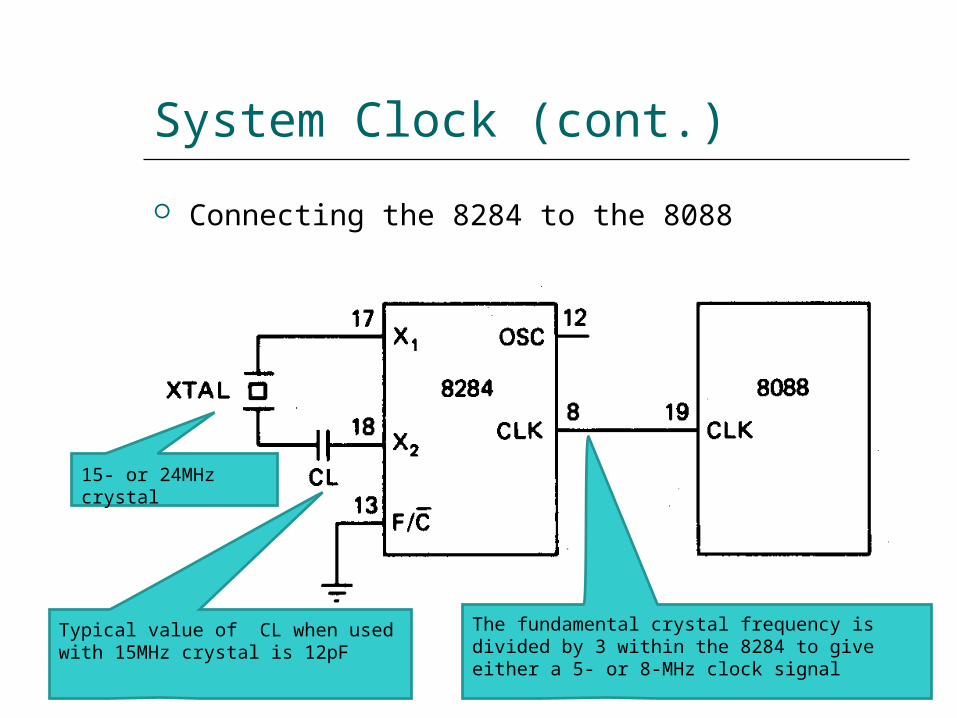
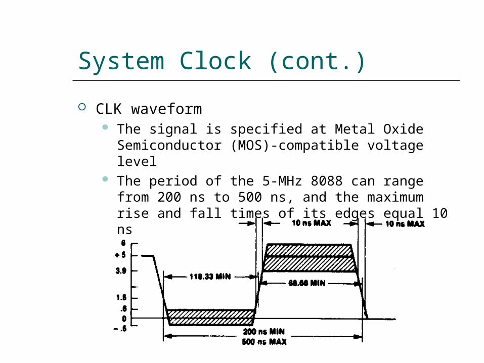
Bus Cycle and Time States (cont)
Bus cycle clock periods idle state and wait state
Bus Cycle and Time States (cont)
EXAMPLE What is the duration of the bus cycle in the 8088-
based microcomputer if the clock is 8 MHz and the two wait states are inserted
Solution The duration of the bus cycle in an 8 MHz system
is given by tcyc = 500 ns + N x 125 ns
In this expression the N stands for the number of waits states For a bus cycle with two wait states we get
tcyc = 500 ns + 2 x 125 ns = 500 ns + 250 ns = 750 ns
Hardware Organization of the Memory Address Space
1Mx8 memory bank of the 8088
Hardware Organization of the Memory Address Space (cont)
High and low memory banks of the 8086
Hardware Organization of the Memory Address Space (cont)
Byte transfer by the 8088
Hardware Organization of the Memory Address Space (cont)
Word transfer by the 8088
Hardware Organization of the Memory Address Space (cont)
Even address byte transfer by the 8086
Hardware Organization of the Memory Address Space (cont)
Odd address byte transfer by the 8086
Hardware Organization of the Memory Address Space (cont)
Even address word transfer by the 8086
Hardware Organization of the Memory Address Space (cont)
Odd-address word transfer by the 8086
Hardware Organization of the Memory Address Space (cont)
EXAMPLE Is the word at memory address 0123116 of an
8086-based microcomputer aligned or misaligned How many cycle are required to read it from memory
Solution The first byte of the word is the second byte at
the aligned-word address 0123016 Therefore the word is misaligned and required two bus cycles to be read from memory
Address Bus Status Codes
Whenever a memory bus cycle is in progress an address bus status code S4S3 is output by the processor S4S3 identifies which one of the four segment
register is used to generate the physical address in the current bus cycle 1048729
S4S3=00 identifies the extra segment register (ES)
S4S3=01 identifies the stack segment register (SS)
S4S3=10 identifies the code segment register (CS)
S4S3=11 identifies the data segment register (DS)
The memory address reach of the microprocessor can thus be expanded to 4 Mbytes
Memory Control Signals
Minimum-mode memory control signals
Memory Control Signals (cont)
Minimum-mode memory control signals (8088) ALE ndash Address Latch Enable ndash used to latch
the address in external memory IOM ndash Input-OutputMemory ndash signal external
circuitry whether a memory of IO bus cycle is in progress
DTR ndash Data TransmitReceive ndash signal external circuitry whether the 8088 is transmitting or receiving data over the bus 1048729
RD ndash Read ndash identifies that a read bus cycle is in progress
WR ndash Write ndash identifies that a write bus cycle is in progress
DEN ndash Data Enable ndash used to enable the data bus 1048729
SSO ndash Status Line ndash identifies whether a code or data access is in progress
Memory Control Signals (cont)
The control signals for the 8086rsquos minimum-mode memory interface differs in three ways IOM signal is replaced by MIO signal The signal SSO is removed from the interface BHE (bank high enable) is added to the interface
and is used to select input for the high bank of memory in the 8086rsquos memory subsystem
Memory Control Signals (cont)
Maximum-mode memory control signals
Memory Control Signals (cont)
Maximum-mode memory control signals MRDC ndash Memory Read Command 1048729 MWTC ndash Memory Write Command 1048729 AMWC ndash Advanced Memory Write Command
Read and Write Bus Cycle
Read cycle
Minimum-mode memory read bus cycle of the 8088
Read and Write Bus Cycle (cont)
Read cycle
Minimum-mode memory read bus cycle of the 8086
Read and Write Bus Cycle (cont)
Read cycle
Maximum-mode memory read bus cycle of the 8086
Read and Write Bus Cycle (cont)
Write cycle
Minimum-mode memory write bus cycle of the 8088
Read and Write Bus Cycle (cont)
Write cycle
Maximum-mode memory write bus cycle of the 8086
Memory Interface Circuit
Address bus latches and buffers Bank write and bank read control logic Data bus transceiversbuffers Address decoders
Memory Interface Circuit (cont)
Memory interface block diagram
Memory Interface Circuit (cont)
Address bus latches and buffers
Block diagram of a D-type latch
Memory Interface Circuit (cont)
Address bus latches and buffers
Circuit diagram of the 74F373
Memory Interface Circuit (cont)
A review of flip-floplatch logic
Positive edge-triggered D flip-flop
Memory Interface Circuit (cont)
A review of flip-floplatch logic
Positive edge-triggered JK flip-flop
Memory Interface Circuit (cont)
A review of flip-floplatch logic
D-type latch
Memory Interface Circuit (cont)
Address bus latches and buffers
Address latch circuit
Memory Interface Circuit (cont)
Bank write and bank read control logic
Bank write control logic Bank read control logic
Memory Interface Circuit (cont)
Data bus transceivers
Block diagram and circuit diagram of the 74F245 octal bus transceiver
Memory Interface Circuit (cont)
Data bus transceivers
Data bus transceiver circuit
Memory Interface Circuit (cont)
Address decoder
Address bus configuration with address decoding
Memory Interface Circuit (cont)
Address decoder
Block diagram and operation of the 74F139 decoder
Memory Interface Circuit (cont)
Address decoder
Circuit diagram of the 74F139 decoder
Memory Interface Circuit (cont)
Address decoder
Address decoder circuit using 74F139
Memory Interface Circuit (cont)
Address decoder
Block diagram and operation of the 74F138 decoder
Memory Interface Circuit (cont)
Address decoder
Circuit diagram of the 74F138 decoder
Memory Interface Circuit (cont)
Address decoder
Address decoder circuit using 74F138
Types of InputOutput
The IO system allows peripherals to provide data or receive results of processing the data Using IO ports
The 80888086 MPU can employ two types of IO Isolated IO Memory-mapped IO
They differ in how IO ports are mapped into the address space
Types of InputOutput (cont)
Isolated inputoutput When using isolated IO in a microcomputer
system the IO device are treated separate from memory
The memory address space contains 1 M consecutive byte address in the range 0000016 through FFFFF16
The IO address space contains 64K consecutive byte addresses in the range 000016 through FFFF16
The bytes in two consecutive IO addresses can be accessed as word-wide data
Page 0 000016 00FF16
Certain IO instructions can only perform in this range
Types of InputOutput (cont)
Isolated inputoutput
80888086 memory and IO address spaces
Types of InputOutput (cont)
Isolated inputoutput
Isolated IO ports
Types of InputOutput (cont)
Isolated inputoutput Advantages
The complete 1Mbyte memory address space is available for use with memory
Special instructions have been provided to perform IO operations with maximized performance
The bytes in two consecutive IO addresses can be accessed as word-wide data
Disadvantages All input and output data transfers must take place
between the AL or AX register and IO port
Types of InputOutput (cont)
Memory-mapped inputoutput MPU looks at the IO port as though it is a storage
location in memory Some of the memory address space is dedicated to IO
ports Instructions that affect data in memory are used
instead of the special IO instructions More instructions and addressing modes are available to
perform IO operations IO transfers can take place between IO port and other
internal registers The memory instructions tend to execute slower
than those specifically designed for isolated IO Part of the memory address space is lost
Types of InputOutput(cont)
Memory-mapped inputoutput
Memory mapped IO ports
Isolated InputOutput Interface
IO devices Keyboard Printer Mouse 82C55A etc
Functions of interface circuit Select the IO port Latch output data Sample input data Synchronize data transfer Translate between TTL voltage levels and those
required to operate the IO devices
Isolated InputOutput Interface (cont)
Minimum-mode interface
Minimum-mode 8088 system IO interface
Isolated InputOutput Interface (cont)
Minimum-mode interface
Minimum-mode 8086 system IO interface
Isolated InputOutput Interface (cont)
Maximum-mode interface
Maximum-mode 8088 system IO interface
Isolated InputOutput Interface (cont)
Maximum-mode interface
Maximum-mode 8086 system IO interface
Isolated InputOutput Interface (cont)
Maximum-mode interface
IO bus cycle status codes
InputOutput Data Transfer
Inputoutput data transfers in the 8088 and 8086 microcomputers can be either byte-wide or word-wide
IO addresses are 16 bits in length and are output by the 8088 to the IO interface over bus lines AD0 through AD7 and A8 through A15
In 8088 the word transfers is performed as two consecutive byte-wide data transfer and takes two bus cycle
In 8086 the word transfers can takes either one or two bus cycle
Word-wide IO ports should be aligned at even-address boundaries
InputOutput Data Instructions
InputOutput Data Instructions(cont)
EXAMPLE Write a sequence of instructions that will output
the data FF16 to a byte-wide output port at address AB16 of the IO address space
Solution First the AL register is loaded with FF16 as an
immediate operand in the instruction
MOV AL 0FFH Now the data in AL can be output to the byte-
wide output port with the instruction
OUT 0ABH AL
InputOutput Data Instructions(cont)
EXAMPLE Write a series of instructions that will output FF16 to an
output port located at address B00016 of the IO address space
Solution The DX register must first be loaded with the address
of the output port This is done with the instructionMOV DX 0B000H
Next the data that are to be output must be loaded into AL with the instruction
MOV AL 0FFH Finally the data are output with the instruction
OUT DX AL
InputOutput Data Instructions(cont)
EXAMPLE Data are to be read in from two byte-wide input
ports at addresses AA16 and A916 and then output as a word-wide output port at address B00016 Write a sequence of instructions to perform this inputoutput operation
InputOutput Data Instructions(cont)
Solution First read in the byte at address AA16 into AL and
move it into AHIN AL 0AAHMOV AH AL
Now the other byte can be read into AL by the instructionIN AL 09AH
And to write out the word of dataMOV DX 0B000HOUT DX AX
InputOutput Bus Cycles
Input bus cycle of the 8088
InputOutput Bus Cycles (cont)
Output bus cycle of the 8088
InputOutput Bus Cycles (cont)
Input bus cycle of the 8086
InputOutput Bus Cycles (cont)
Output bus cycle of the 8086
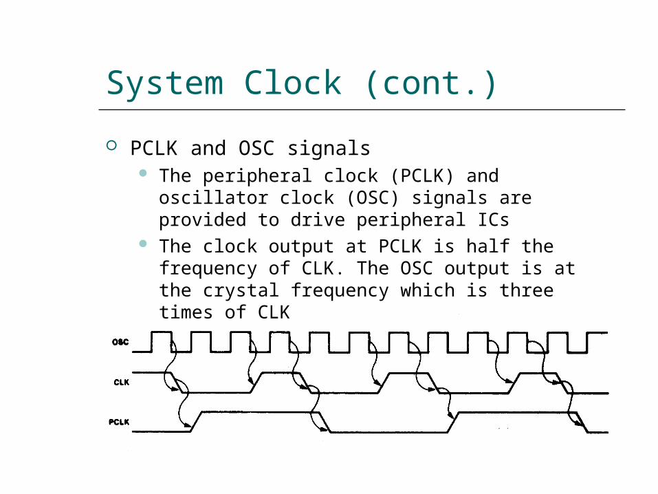
Bus Cycle and Time States (cont)
EXAMPLE What is the duration of the bus cycle in the 8088-
based microcomputer if the clock is 8 MHz and the two wait states are inserted
Solution The duration of the bus cycle in an 8 MHz system
is given by tcyc = 500 ns + N x 125 ns
In this expression the N stands for the number of waits states For a bus cycle with two wait states we get
tcyc = 500 ns + 2 x 125 ns = 500 ns + 250 ns = 750 ns
Hardware Organization of the Memory Address Space
1Mx8 memory bank of the 8088
Hardware Organization of the Memory Address Space (cont)
High and low memory banks of the 8086
Hardware Organization of the Memory Address Space (cont)
Byte transfer by the 8088
Hardware Organization of the Memory Address Space (cont)
Word transfer by the 8088
Hardware Organization of the Memory Address Space (cont)
Even address byte transfer by the 8086
Hardware Organization of the Memory Address Space (cont)
Odd address byte transfer by the 8086
Hardware Organization of the Memory Address Space (cont)
Even address word transfer by the 8086
Hardware Organization of the Memory Address Space (cont)
Odd-address word transfer by the 8086
Hardware Organization of the Memory Address Space (cont)
EXAMPLE Is the word at memory address 0123116 of an
8086-based microcomputer aligned or misaligned How many cycle are required to read it from memory
Solution The first byte of the word is the second byte at
the aligned-word address 0123016 Therefore the word is misaligned and required two bus cycles to be read from memory
Address Bus Status Codes
Whenever a memory bus cycle is in progress an address bus status code S4S3 is output by the processor S4S3 identifies which one of the four segment
register is used to generate the physical address in the current bus cycle 1048729
S4S3=00 identifies the extra segment register (ES)
S4S3=01 identifies the stack segment register (SS)
S4S3=10 identifies the code segment register (CS)
S4S3=11 identifies the data segment register (DS)
The memory address reach of the microprocessor can thus be expanded to 4 Mbytes
Memory Control Signals
Minimum-mode memory control signals
Memory Control Signals (cont)
Minimum-mode memory control signals (8088) ALE ndash Address Latch Enable ndash used to latch
the address in external memory IOM ndash Input-OutputMemory ndash signal external
circuitry whether a memory of IO bus cycle is in progress
DTR ndash Data TransmitReceive ndash signal external circuitry whether the 8088 is transmitting or receiving data over the bus 1048729
RD ndash Read ndash identifies that a read bus cycle is in progress
WR ndash Write ndash identifies that a write bus cycle is in progress
DEN ndash Data Enable ndash used to enable the data bus 1048729
SSO ndash Status Line ndash identifies whether a code or data access is in progress
Memory Control Signals (cont)
The control signals for the 8086rsquos minimum-mode memory interface differs in three ways IOM signal is replaced by MIO signal The signal SSO is removed from the interface BHE (bank high enable) is added to the interface
and is used to select input for the high bank of memory in the 8086rsquos memory subsystem
Memory Control Signals (cont)
Maximum-mode memory control signals
Memory Control Signals (cont)
Maximum-mode memory control signals MRDC ndash Memory Read Command 1048729 MWTC ndash Memory Write Command 1048729 AMWC ndash Advanced Memory Write Command
Read and Write Bus Cycle
Read cycle
Minimum-mode memory read bus cycle of the 8088
Read and Write Bus Cycle (cont)
Read cycle
Minimum-mode memory read bus cycle of the 8086
Read and Write Bus Cycle (cont)
Read cycle
Maximum-mode memory read bus cycle of the 8086
Read and Write Bus Cycle (cont)
Write cycle
Minimum-mode memory write bus cycle of the 8088
Read and Write Bus Cycle (cont)
Write cycle
Maximum-mode memory write bus cycle of the 8086
Memory Interface Circuit
Address bus latches and buffers Bank write and bank read control logic Data bus transceiversbuffers Address decoders
Memory Interface Circuit (cont)
Memory interface block diagram
Memory Interface Circuit (cont)
Address bus latches and buffers
Block diagram of a D-type latch
Memory Interface Circuit (cont)
Address bus latches and buffers
Circuit diagram of the 74F373
Memory Interface Circuit (cont)
A review of flip-floplatch logic
Positive edge-triggered D flip-flop
Memory Interface Circuit (cont)
A review of flip-floplatch logic
Positive edge-triggered JK flip-flop
Memory Interface Circuit (cont)
A review of flip-floplatch logic
D-type latch
Memory Interface Circuit (cont)
Address bus latches and buffers
Address latch circuit
Memory Interface Circuit (cont)
Bank write and bank read control logic
Bank write control logic Bank read control logic
Memory Interface Circuit (cont)
Data bus transceivers
Block diagram and circuit diagram of the 74F245 octal bus transceiver
Memory Interface Circuit (cont)
Data bus transceivers
Data bus transceiver circuit
Memory Interface Circuit (cont)
Address decoder
Address bus configuration with address decoding
Memory Interface Circuit (cont)
Address decoder
Block diagram and operation of the 74F139 decoder
Memory Interface Circuit (cont)
Address decoder
Circuit diagram of the 74F139 decoder
Memory Interface Circuit (cont)
Address decoder
Address decoder circuit using 74F139
Memory Interface Circuit (cont)
Address decoder
Block diagram and operation of the 74F138 decoder
Memory Interface Circuit (cont)
Address decoder
Circuit diagram of the 74F138 decoder
Memory Interface Circuit (cont)
Address decoder
Address decoder circuit using 74F138
Types of InputOutput
The IO system allows peripherals to provide data or receive results of processing the data Using IO ports
The 80888086 MPU can employ two types of IO Isolated IO Memory-mapped IO
They differ in how IO ports are mapped into the address space
Types of InputOutput (cont)
Isolated inputoutput When using isolated IO in a microcomputer
system the IO device are treated separate from memory
The memory address space contains 1 M consecutive byte address in the range 0000016 through FFFFF16
The IO address space contains 64K consecutive byte addresses in the range 000016 through FFFF16
The bytes in two consecutive IO addresses can be accessed as word-wide data
Page 0 000016 00FF16
Certain IO instructions can only perform in this range
Types of InputOutput (cont)
Isolated inputoutput
80888086 memory and IO address spaces
Types of InputOutput (cont)
Isolated inputoutput
Isolated IO ports
Types of InputOutput (cont)
Isolated inputoutput Advantages
The complete 1Mbyte memory address space is available for use with memory
Special instructions have been provided to perform IO operations with maximized performance
The bytes in two consecutive IO addresses can be accessed as word-wide data
Disadvantages All input and output data transfers must take place
between the AL or AX register and IO port
Types of InputOutput (cont)
Memory-mapped inputoutput MPU looks at the IO port as though it is a storage
location in memory Some of the memory address space is dedicated to IO
ports Instructions that affect data in memory are used
instead of the special IO instructions More instructions and addressing modes are available to
perform IO operations IO transfers can take place between IO port and other
internal registers The memory instructions tend to execute slower
than those specifically designed for isolated IO Part of the memory address space is lost
Types of InputOutput(cont)
Memory-mapped inputoutput
Memory mapped IO ports
Isolated InputOutput Interface
IO devices Keyboard Printer Mouse 82C55A etc
Functions of interface circuit Select the IO port Latch output data Sample input data Synchronize data transfer Translate between TTL voltage levels and those
required to operate the IO devices
Isolated InputOutput Interface (cont)
Minimum-mode interface
Minimum-mode 8088 system IO interface
Isolated InputOutput Interface (cont)
Minimum-mode interface
Minimum-mode 8086 system IO interface
Isolated InputOutput Interface (cont)
Maximum-mode interface
Maximum-mode 8088 system IO interface
Isolated InputOutput Interface (cont)
Maximum-mode interface
Maximum-mode 8086 system IO interface
Isolated InputOutput Interface (cont)
Maximum-mode interface
IO bus cycle status codes
InputOutput Data Transfer
Inputoutput data transfers in the 8088 and 8086 microcomputers can be either byte-wide or word-wide
IO addresses are 16 bits in length and are output by the 8088 to the IO interface over bus lines AD0 through AD7 and A8 through A15
In 8088 the word transfers is performed as two consecutive byte-wide data transfer and takes two bus cycle
In 8086 the word transfers can takes either one or two bus cycle
Word-wide IO ports should be aligned at even-address boundaries
InputOutput Data Instructions
InputOutput Data Instructions(cont)
EXAMPLE Write a sequence of instructions that will output
the data FF16 to a byte-wide output port at address AB16 of the IO address space
Solution First the AL register is loaded with FF16 as an
immediate operand in the instruction
MOV AL 0FFH Now the data in AL can be output to the byte-
wide output port with the instruction
OUT 0ABH AL
InputOutput Data Instructions(cont)
EXAMPLE Write a series of instructions that will output FF16 to an
output port located at address B00016 of the IO address space
Solution The DX register must first be loaded with the address
of the output port This is done with the instructionMOV DX 0B000H
Next the data that are to be output must be loaded into AL with the instruction
MOV AL 0FFH Finally the data are output with the instruction
OUT DX AL
InputOutput Data Instructions(cont)
EXAMPLE Data are to be read in from two byte-wide input
ports at addresses AA16 and A916 and then output as a word-wide output port at address B00016 Write a sequence of instructions to perform this inputoutput operation
InputOutput Data Instructions(cont)
Solution First read in the byte at address AA16 into AL and
move it into AHIN AL 0AAHMOV AH AL
Now the other byte can be read into AL by the instructionIN AL 09AH
And to write out the word of dataMOV DX 0B000HOUT DX AX
InputOutput Bus Cycles
Input bus cycle of the 8088
InputOutput Bus Cycles (cont)
Output bus cycle of the 8088
InputOutput Bus Cycles (cont)
Input bus cycle of the 8086
InputOutput Bus Cycles (cont)
Output bus cycle of the 8086
Hardware Organization of the Memory Address Space (cont)
Byte transfer by the 8088
Hardware Organization of the Memory Address Space (cont)
Word transfer by the 8088
Hardware Organization of the Memory Address Space (cont)
Even address byte transfer by the 8086
Hardware Organization of the Memory Address Space (cont)
Odd address byte transfer by the 8086
Hardware Organization of the Memory Address Space (cont)
Even address word transfer by the 8086
Hardware Organization of the Memory Address Space (cont)
Odd-address word transfer by the 8086
Hardware Organization of the Memory Address Space (cont)
EXAMPLE Is the word at memory address 0123116 of an
8086-based microcomputer aligned or misaligned How many cycle are required to read it from memory
Solution The first byte of the word is the second byte at
the aligned-word address 0123016 Therefore the word is misaligned and required two bus cycles to be read from memory
Address Bus Status Codes
Whenever a memory bus cycle is in progress an address bus status code S4S3 is output by the processor S4S3 identifies which one of the four segment
register is used to generate the physical address in the current bus cycle 1048729
S4S3=00 identifies the extra segment register (ES)
S4S3=01 identifies the stack segment register (SS)
S4S3=10 identifies the code segment register (CS)
S4S3=11 identifies the data segment register (DS)
The memory address reach of the microprocessor can thus be expanded to 4 Mbytes
Memory Control Signals
Minimum-mode memory control signals
Memory Control Signals (cont)
Minimum-mode memory control signals (8088) ALE ndash Address Latch Enable ndash used to latch
the address in external memory IOM ndash Input-OutputMemory ndash signal external
circuitry whether a memory of IO bus cycle is in progress
DTR ndash Data TransmitReceive ndash signal external circuitry whether the 8088 is transmitting or receiving data over the bus 1048729
RD ndash Read ndash identifies that a read bus cycle is in progress
WR ndash Write ndash identifies that a write bus cycle is in progress
DEN ndash Data Enable ndash used to enable the data bus 1048729
SSO ndash Status Line ndash identifies whether a code or data access is in progress
Memory Control Signals (cont)
The control signals for the 8086rsquos minimum-mode memory interface differs in three ways IOM signal is replaced by MIO signal The signal SSO is removed from the interface BHE (bank high enable) is added to the interface
and is used to select input for the high bank of memory in the 8086rsquos memory subsystem
Memory Control Signals (cont)
Maximum-mode memory control signals
Memory Control Signals (cont)
Maximum-mode memory control signals MRDC ndash Memory Read Command 1048729 MWTC ndash Memory Write Command 1048729 AMWC ndash Advanced Memory Write Command
Read and Write Bus Cycle
Read cycle
Minimum-mode memory read bus cycle of the 8088
Read and Write Bus Cycle (cont)
Read cycle
Minimum-mode memory read bus cycle of the 8086
Read and Write Bus Cycle (cont)
Read cycle
Maximum-mode memory read bus cycle of the 8086
Read and Write Bus Cycle (cont)
Write cycle
Minimum-mode memory write bus cycle of the 8088
Read and Write Bus Cycle (cont)
Write cycle
Maximum-mode memory write bus cycle of the 8086
Memory Interface Circuit
Address bus latches and buffers Bank write and bank read control logic Data bus transceiversbuffers Address decoders
Memory Interface Circuit (cont)
Memory interface block diagram
Memory Interface Circuit (cont)
Address bus latches and buffers
Block diagram of a D-type latch
Memory Interface Circuit (cont)
Address bus latches and buffers
Circuit diagram of the 74F373
Memory Interface Circuit (cont)
A review of flip-floplatch logic
Positive edge-triggered D flip-flop
Memory Interface Circuit (cont)
A review of flip-floplatch logic
Positive edge-triggered JK flip-flop
Memory Interface Circuit (cont)
A review of flip-floplatch logic
D-type latch
Memory Interface Circuit (cont)
Address bus latches and buffers
Address latch circuit
Memory Interface Circuit (cont)
Bank write and bank read control logic
Bank write control logic Bank read control logic
Memory Interface Circuit (cont)
Data bus transceivers
Block diagram and circuit diagram of the 74F245 octal bus transceiver
Memory Interface Circuit (cont)
Data bus transceivers
Data bus transceiver circuit
Memory Interface Circuit (cont)
Address decoder
Address bus configuration with address decoding
Memory Interface Circuit (cont)
Address decoder
Block diagram and operation of the 74F139 decoder
Memory Interface Circuit (cont)
Address decoder
Circuit diagram of the 74F139 decoder
Memory Interface Circuit (cont)
Address decoder
Address decoder circuit using 74F139
Memory Interface Circuit (cont)
Address decoder
Block diagram and operation of the 74F138 decoder
Memory Interface Circuit (cont)
Address decoder
Circuit diagram of the 74F138 decoder
Memory Interface Circuit (cont)
Address decoder
Address decoder circuit using 74F138
Types of InputOutput
The IO system allows peripherals to provide data or receive results of processing the data Using IO ports
The 80888086 MPU can employ two types of IO Isolated IO Memory-mapped IO
They differ in how IO ports are mapped into the address space
Types of InputOutput (cont)
Isolated inputoutput When using isolated IO in a microcomputer
system the IO device are treated separate from memory
The memory address space contains 1 M consecutive byte address in the range 0000016 through FFFFF16
The IO address space contains 64K consecutive byte addresses in the range 000016 through FFFF16
The bytes in two consecutive IO addresses can be accessed as word-wide data
Page 0 000016 00FF16
Certain IO instructions can only perform in this range
Types of InputOutput (cont)
Isolated inputoutput
80888086 memory and IO address spaces
Types of InputOutput (cont)
Isolated inputoutput
Isolated IO ports
Types of InputOutput (cont)
Isolated inputoutput Advantages
The complete 1Mbyte memory address space is available for use with memory
Special instructions have been provided to perform IO operations with maximized performance
The bytes in two consecutive IO addresses can be accessed as word-wide data
Disadvantages All input and output data transfers must take place
between the AL or AX register and IO port
Types of InputOutput (cont)
Memory-mapped inputoutput MPU looks at the IO port as though it is a storage
location in memory Some of the memory address space is dedicated to IO
ports Instructions that affect data in memory are used
instead of the special IO instructions More instructions and addressing modes are available to
perform IO operations IO transfers can take place between IO port and other
internal registers The memory instructions tend to execute slower
than those specifically designed for isolated IO Part of the memory address space is lost
Types of InputOutput(cont)
Memory-mapped inputoutput
Memory mapped IO ports
Isolated InputOutput Interface
IO devices Keyboard Printer Mouse 82C55A etc
Functions of interface circuit Select the IO port Latch output data Sample input data Synchronize data transfer Translate between TTL voltage levels and those
required to operate the IO devices
Isolated InputOutput Interface (cont)
Minimum-mode interface
Minimum-mode 8088 system IO interface
Isolated InputOutput Interface (cont)
Minimum-mode interface
Minimum-mode 8086 system IO interface
Isolated InputOutput Interface (cont)
Maximum-mode interface
Maximum-mode 8088 system IO interface
Isolated InputOutput Interface (cont)
Maximum-mode interface
Maximum-mode 8086 system IO interface
Isolated InputOutput Interface (cont)
Maximum-mode interface
IO bus cycle status codes
InputOutput Data Transfer
Inputoutput data transfers in the 8088 and 8086 microcomputers can be either byte-wide or word-wide
IO addresses are 16 bits in length and are output by the 8088 to the IO interface over bus lines AD0 through AD7 and A8 through A15
In 8088 the word transfers is performed as two consecutive byte-wide data transfer and takes two bus cycle
In 8086 the word transfers can takes either one or two bus cycle
Word-wide IO ports should be aligned at even-address boundaries
InputOutput Data Instructions
InputOutput Data Instructions(cont)
EXAMPLE Write a sequence of instructions that will output
the data FF16 to a byte-wide output port at address AB16 of the IO address space
Solution First the AL register is loaded with FF16 as an
immediate operand in the instruction
MOV AL 0FFH Now the data in AL can be output to the byte-
wide output port with the instruction
OUT 0ABH AL
InputOutput Data Instructions(cont)
EXAMPLE Write a series of instructions that will output FF16 to an
output port located at address B00016 of the IO address space
Solution The DX register must first be loaded with the address
of the output port This is done with the instructionMOV DX 0B000H
Next the data that are to be output must be loaded into AL with the instruction
MOV AL 0FFH Finally the data are output with the instruction
OUT DX AL
InputOutput Data Instructions(cont)
EXAMPLE Data are to be read in from two byte-wide input
ports at addresses AA16 and A916 and then output as a word-wide output port at address B00016 Write a sequence of instructions to perform this inputoutput operation
InputOutput Data Instructions(cont)
Solution First read in the byte at address AA16 into AL and
move it into AHIN AL 0AAHMOV AH AL
Now the other byte can be read into AL by the instructionIN AL 09AH
And to write out the word of dataMOV DX 0B000HOUT DX AX
InputOutput Bus Cycles
Input bus cycle of the 8088
InputOutput Bus Cycles (cont)
Output bus cycle of the 8088
InputOutput Bus Cycles (cont)
Input bus cycle of the 8086
InputOutput Bus Cycles (cont)
Output bus cycle of the 8086
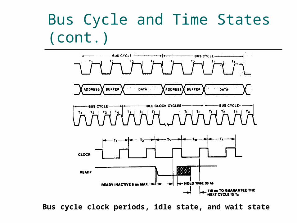
Hardware Organization of the Memory Address Space (cont)
Word transfer by the 8088
Hardware Organization of the Memory Address Space (cont)
Even address byte transfer by the 8086
Hardware Organization of the Memory Address Space (cont)
Odd address byte transfer by the 8086
Hardware Organization of the Memory Address Space (cont)
Even address word transfer by the 8086
Hardware Organization of the Memory Address Space (cont)
Odd-address word transfer by the 8086
Hardware Organization of the Memory Address Space (cont)
EXAMPLE Is the word at memory address 0123116 of an
8086-based microcomputer aligned or misaligned How many cycle are required to read it from memory
Solution The first byte of the word is the second byte at
the aligned-word address 0123016 Therefore the word is misaligned and required two bus cycles to be read from memory
Address Bus Status Codes
Whenever a memory bus cycle is in progress an address bus status code S4S3 is output by the processor S4S3 identifies which one of the four segment
register is used to generate the physical address in the current bus cycle 1048729
S4S3=00 identifies the extra segment register (ES)
S4S3=01 identifies the stack segment register (SS)
S4S3=10 identifies the code segment register (CS)
S4S3=11 identifies the data segment register (DS)
The memory address reach of the microprocessor can thus be expanded to 4 Mbytes
Memory Control Signals
Minimum-mode memory control signals
Memory Control Signals (cont)
Minimum-mode memory control signals (8088) ALE ndash Address Latch Enable ndash used to latch
the address in external memory IOM ndash Input-OutputMemory ndash signal external
circuitry whether a memory of IO bus cycle is in progress
DTR ndash Data TransmitReceive ndash signal external circuitry whether the 8088 is transmitting or receiving data over the bus 1048729
RD ndash Read ndash identifies that a read bus cycle is in progress
WR ndash Write ndash identifies that a write bus cycle is in progress
DEN ndash Data Enable ndash used to enable the data bus 1048729
SSO ndash Status Line ndash identifies whether a code or data access is in progress
Memory Control Signals (cont)
The control signals for the 8086rsquos minimum-mode memory interface differs in three ways IOM signal is replaced by MIO signal The signal SSO is removed from the interface BHE (bank high enable) is added to the interface
and is used to select input for the high bank of memory in the 8086rsquos memory subsystem
Memory Control Signals (cont)
Maximum-mode memory control signals
Memory Control Signals (cont)
Maximum-mode memory control signals MRDC ndash Memory Read Command 1048729 MWTC ndash Memory Write Command 1048729 AMWC ndash Advanced Memory Write Command
Read and Write Bus Cycle
Read cycle
Minimum-mode memory read bus cycle of the 8088
Read and Write Bus Cycle (cont)
Read cycle
Minimum-mode memory read bus cycle of the 8086
Read and Write Bus Cycle (cont)
Read cycle
Maximum-mode memory read bus cycle of the 8086
Read and Write Bus Cycle (cont)
Write cycle
Minimum-mode memory write bus cycle of the 8088
Read and Write Bus Cycle (cont)
Write cycle
Maximum-mode memory write bus cycle of the 8086
Memory Interface Circuit
Address bus latches and buffers Bank write and bank read control logic Data bus transceiversbuffers Address decoders
Memory Interface Circuit (cont)
Memory interface block diagram
Memory Interface Circuit (cont)
Address bus latches and buffers
Block diagram of a D-type latch
Memory Interface Circuit (cont)
Address bus latches and buffers
Circuit diagram of the 74F373
Memory Interface Circuit (cont)
A review of flip-floplatch logic
Positive edge-triggered D flip-flop
Memory Interface Circuit (cont)
A review of flip-floplatch logic
Positive edge-triggered JK flip-flop
Memory Interface Circuit (cont)
A review of flip-floplatch logic
D-type latch
Memory Interface Circuit (cont)
Address bus latches and buffers
Address latch circuit
Memory Interface Circuit (cont)
Bank write and bank read control logic
Bank write control logic Bank read control logic
Memory Interface Circuit (cont)
Data bus transceivers
Block diagram and circuit diagram of the 74F245 octal bus transceiver
Memory Interface Circuit (cont)
Data bus transceivers
Data bus transceiver circuit
Memory Interface Circuit (cont)
Address decoder
Address bus configuration with address decoding
Memory Interface Circuit (cont)
Address decoder
Block diagram and operation of the 74F139 decoder
Memory Interface Circuit (cont)
Address decoder
Circuit diagram of the 74F139 decoder
Memory Interface Circuit (cont)
Address decoder
Address decoder circuit using 74F139
Memory Interface Circuit (cont)
Address decoder
Block diagram and operation of the 74F138 decoder
Memory Interface Circuit (cont)
Address decoder
Circuit diagram of the 74F138 decoder
Memory Interface Circuit (cont)
Address decoder
Address decoder circuit using 74F138
Types of InputOutput
The IO system allows peripherals to provide data or receive results of processing the data Using IO ports
The 80888086 MPU can employ two types of IO Isolated IO Memory-mapped IO
They differ in how IO ports are mapped into the address space
Types of InputOutput (cont)
Isolated inputoutput When using isolated IO in a microcomputer
system the IO device are treated separate from memory
The memory address space contains 1 M consecutive byte address in the range 0000016 through FFFFF16
The IO address space contains 64K consecutive byte addresses in the range 000016 through FFFF16
The bytes in two consecutive IO addresses can be accessed as word-wide data
Page 0 000016 00FF16
Certain IO instructions can only perform in this range
Types of InputOutput (cont)
Isolated inputoutput
80888086 memory and IO address spaces
Types of InputOutput (cont)
Isolated inputoutput
Isolated IO ports
Types of InputOutput (cont)
Isolated inputoutput Advantages
The complete 1Mbyte memory address space is available for use with memory
Special instructions have been provided to perform IO operations with maximized performance
The bytes in two consecutive IO addresses can be accessed as word-wide data
Disadvantages All input and output data transfers must take place
between the AL or AX register and IO port
Types of InputOutput (cont)
Memory-mapped inputoutput MPU looks at the IO port as though it is a storage
location in memory Some of the memory address space is dedicated to IO
ports Instructions that affect data in memory are used
instead of the special IO instructions More instructions and addressing modes are available to
perform IO operations IO transfers can take place between IO port and other
internal registers The memory instructions tend to execute slower
than those specifically designed for isolated IO Part of the memory address space is lost
Types of InputOutput(cont)
Memory-mapped inputoutput
Memory mapped IO ports
Isolated InputOutput Interface
IO devices Keyboard Printer Mouse 82C55A etc
Functions of interface circuit Select the IO port Latch output data Sample input data Synchronize data transfer Translate between TTL voltage levels and those
required to operate the IO devices
Isolated InputOutput Interface (cont)
Minimum-mode interface
Minimum-mode 8088 system IO interface
Isolated InputOutput Interface (cont)
Minimum-mode interface
Minimum-mode 8086 system IO interface
Isolated InputOutput Interface (cont)
Maximum-mode interface
Maximum-mode 8088 system IO interface
Isolated InputOutput Interface (cont)
Maximum-mode interface
Maximum-mode 8086 system IO interface
Isolated InputOutput Interface (cont)
Maximum-mode interface
IO bus cycle status codes
InputOutput Data Transfer
Inputoutput data transfers in the 8088 and 8086 microcomputers can be either byte-wide or word-wide
IO addresses are 16 bits in length and are output by the 8088 to the IO interface over bus lines AD0 through AD7 and A8 through A15
In 8088 the word transfers is performed as two consecutive byte-wide data transfer and takes two bus cycle
In 8086 the word transfers can takes either one or two bus cycle
Word-wide IO ports should be aligned at even-address boundaries
InputOutput Data Instructions
InputOutput Data Instructions(cont)
EXAMPLE Write a sequence of instructions that will output
the data FF16 to a byte-wide output port at address AB16 of the IO address space
Solution First the AL register is loaded with FF16 as an
immediate operand in the instruction
MOV AL 0FFH Now the data in AL can be output to the byte-
wide output port with the instruction
OUT 0ABH AL
InputOutput Data Instructions(cont)
EXAMPLE Write a series of instructions that will output FF16 to an
output port located at address B00016 of the IO address space
Solution The DX register must first be loaded with the address
of the output port This is done with the instructionMOV DX 0B000H
Next the data that are to be output must be loaded into AL with the instruction
MOV AL 0FFH Finally the data are output with the instruction
OUT DX AL
InputOutput Data Instructions(cont)
EXAMPLE Data are to be read in from two byte-wide input
ports at addresses AA16 and A916 and then output as a word-wide output port at address B00016 Write a sequence of instructions to perform this inputoutput operation
InputOutput Data Instructions(cont)
Solution First read in the byte at address AA16 into AL and
move it into AHIN AL 0AAHMOV AH AL
Now the other byte can be read into AL by the instructionIN AL 09AH
And to write out the word of dataMOV DX 0B000HOUT DX AX
InputOutput Bus Cycles
Input bus cycle of the 8088
InputOutput Bus Cycles (cont)
Output bus cycle of the 8088
InputOutput Bus Cycles (cont)
Input bus cycle of the 8086
InputOutput Bus Cycles (cont)
Output bus cycle of the 8086
Hardware Organization of the Memory Address Space (cont)
Even address byte transfer by the 8086
Hardware Organization of the Memory Address Space (cont)
Odd address byte transfer by the 8086
Hardware Organization of the Memory Address Space (cont)
Even address word transfer by the 8086
Hardware Organization of the Memory Address Space (cont)
Odd-address word transfer by the 8086
Hardware Organization of the Memory Address Space (cont)
EXAMPLE Is the word at memory address 0123116 of an
8086-based microcomputer aligned or misaligned How many cycle are required to read it from memory
Solution The first byte of the word is the second byte at
the aligned-word address 0123016 Therefore the word is misaligned and required two bus cycles to be read from memory
Address Bus Status Codes
Whenever a memory bus cycle is in progress an address bus status code S4S3 is output by the processor S4S3 identifies which one of the four segment
register is used to generate the physical address in the current bus cycle 1048729
S4S3=00 identifies the extra segment register (ES)
S4S3=01 identifies the stack segment register (SS)
S4S3=10 identifies the code segment register (CS)
S4S3=11 identifies the data segment register (DS)
The memory address reach of the microprocessor can thus be expanded to 4 Mbytes
Memory Control Signals
Minimum-mode memory control signals
Memory Control Signals (cont)
Minimum-mode memory control signals (8088) ALE ndash Address Latch Enable ndash used to latch
the address in external memory IOM ndash Input-OutputMemory ndash signal external
circuitry whether a memory of IO bus cycle is in progress
DTR ndash Data TransmitReceive ndash signal external circuitry whether the 8088 is transmitting or receiving data over the bus 1048729
RD ndash Read ndash identifies that a read bus cycle is in progress
WR ndash Write ndash identifies that a write bus cycle is in progress
DEN ndash Data Enable ndash used to enable the data bus 1048729
SSO ndash Status Line ndash identifies whether a code or data access is in progress
Memory Control Signals (cont)
The control signals for the 8086rsquos minimum-mode memory interface differs in three ways IOM signal is replaced by MIO signal The signal SSO is removed from the interface BHE (bank high enable) is added to the interface
and is used to select input for the high bank of memory in the 8086rsquos memory subsystem
Memory Control Signals (cont)
Maximum-mode memory control signals
Memory Control Signals (cont)
Maximum-mode memory control signals MRDC ndash Memory Read Command 1048729 MWTC ndash Memory Write Command 1048729 AMWC ndash Advanced Memory Write Command
Read and Write Bus Cycle
Read cycle
Minimum-mode memory read bus cycle of the 8088
Read and Write Bus Cycle (cont)
Read cycle
Minimum-mode memory read bus cycle of the 8086
Read and Write Bus Cycle (cont)
Read cycle
Maximum-mode memory read bus cycle of the 8086
Read and Write Bus Cycle (cont)
Write cycle
Minimum-mode memory write bus cycle of the 8088
Read and Write Bus Cycle (cont)
Write cycle
Maximum-mode memory write bus cycle of the 8086
Memory Interface Circuit
Address bus latches and buffers Bank write and bank read control logic Data bus transceiversbuffers Address decoders
Memory Interface Circuit (cont)
Memory interface block diagram
Memory Interface Circuit (cont)
Address bus latches and buffers
Block diagram of a D-type latch
Memory Interface Circuit (cont)
Address bus latches and buffers
Circuit diagram of the 74F373
Memory Interface Circuit (cont)
A review of flip-floplatch logic
Positive edge-triggered D flip-flop
Memory Interface Circuit (cont)
A review of flip-floplatch logic
Positive edge-triggered JK flip-flop
Memory Interface Circuit (cont)
A review of flip-floplatch logic
D-type latch
Memory Interface Circuit (cont)
Address bus latches and buffers
Address latch circuit
Memory Interface Circuit (cont)
Bank write and bank read control logic
Bank write control logic Bank read control logic
Memory Interface Circuit (cont)
Data bus transceivers
Block diagram and circuit diagram of the 74F245 octal bus transceiver
Memory Interface Circuit (cont)
Data bus transceivers
Data bus transceiver circuit
Memory Interface Circuit (cont)
Address decoder
Address bus configuration with address decoding
Memory Interface Circuit (cont)
Address decoder
Block diagram and operation of the 74F139 decoder
Memory Interface Circuit (cont)
Address decoder
Circuit diagram of the 74F139 decoder
Memory Interface Circuit (cont)
Address decoder
Address decoder circuit using 74F139
Memory Interface Circuit (cont)
Address decoder
Block diagram and operation of the 74F138 decoder
Memory Interface Circuit (cont)
Address decoder
Circuit diagram of the 74F138 decoder
Memory Interface Circuit (cont)
Address decoder
Address decoder circuit using 74F138
Types of InputOutput
The IO system allows peripherals to provide data or receive results of processing the data Using IO ports
The 80888086 MPU can employ two types of IO Isolated IO Memory-mapped IO
They differ in how IO ports are mapped into the address space
Types of InputOutput (cont)
Isolated inputoutput When using isolated IO in a microcomputer
system the IO device are treated separate from memory
The memory address space contains 1 M consecutive byte address in the range 0000016 through FFFFF16
The IO address space contains 64K consecutive byte addresses in the range 000016 through FFFF16
The bytes in two consecutive IO addresses can be accessed as word-wide data
Page 0 000016 00FF16
Certain IO instructions can only perform in this range
Types of InputOutput (cont)
Isolated inputoutput
80888086 memory and IO address spaces
Types of InputOutput (cont)
Isolated inputoutput
Isolated IO ports
Types of InputOutput (cont)
Isolated inputoutput Advantages
The complete 1Mbyte memory address space is available for use with memory
Special instructions have been provided to perform IO operations with maximized performance
The bytes in two consecutive IO addresses can be accessed as word-wide data
Disadvantages All input and output data transfers must take place
between the AL or AX register and IO port
Types of InputOutput (cont)
Memory-mapped inputoutput MPU looks at the IO port as though it is a storage
location in memory Some of the memory address space is dedicated to IO
ports Instructions that affect data in memory are used
instead of the special IO instructions More instructions and addressing modes are available to
perform IO operations IO transfers can take place between IO port and other
internal registers The memory instructions tend to execute slower
than those specifically designed for isolated IO Part of the memory address space is lost
Types of InputOutput(cont)
Memory-mapped inputoutput
Memory mapped IO ports
Isolated InputOutput Interface
IO devices Keyboard Printer Mouse 82C55A etc
Functions of interface circuit Select the IO port Latch output data Sample input data Synchronize data transfer Translate between TTL voltage levels and those
required to operate the IO devices
Isolated InputOutput Interface (cont)
Minimum-mode interface
Minimum-mode 8088 system IO interface
Isolated InputOutput Interface (cont)
Minimum-mode interface
Minimum-mode 8086 system IO interface
Isolated InputOutput Interface (cont)
Maximum-mode interface
Maximum-mode 8088 system IO interface
Isolated InputOutput Interface (cont)
Maximum-mode interface
Maximum-mode 8086 system IO interface
Isolated InputOutput Interface (cont)
Maximum-mode interface
IO bus cycle status codes
InputOutput Data Transfer
Inputoutput data transfers in the 8088 and 8086 microcomputers can be either byte-wide or word-wide
IO addresses are 16 bits in length and are output by the 8088 to the IO interface over bus lines AD0 through AD7 and A8 through A15
In 8088 the word transfers is performed as two consecutive byte-wide data transfer and takes two bus cycle
In 8086 the word transfers can takes either one or two bus cycle
Word-wide IO ports should be aligned at even-address boundaries
InputOutput Data Instructions
InputOutput Data Instructions(cont)
EXAMPLE Write a sequence of instructions that will output
the data FF16 to a byte-wide output port at address AB16 of the IO address space
Solution First the AL register is loaded with FF16 as an
immediate operand in the instruction
MOV AL 0FFH Now the data in AL can be output to the byte-
wide output port with the instruction
OUT 0ABH AL
InputOutput Data Instructions(cont)
EXAMPLE Write a series of instructions that will output FF16 to an
output port located at address B00016 of the IO address space
Solution The DX register must first be loaded with the address
of the output port This is done with the instructionMOV DX 0B000H
Next the data that are to be output must be loaded into AL with the instruction
MOV AL 0FFH Finally the data are output with the instruction
OUT DX AL
InputOutput Data Instructions(cont)
EXAMPLE Data are to be read in from two byte-wide input
ports at addresses AA16 and A916 and then output as a word-wide output port at address B00016 Write a sequence of instructions to perform this inputoutput operation
InputOutput Data Instructions(cont)
Solution First read in the byte at address AA16 into AL and
move it into AHIN AL 0AAHMOV AH AL
Now the other byte can be read into AL by the instructionIN AL 09AH
And to write out the word of dataMOV DX 0B000HOUT DX AX
InputOutput Bus Cycles
Input bus cycle of the 8088
InputOutput Bus Cycles (cont)
Output bus cycle of the 8088
InputOutput Bus Cycles (cont)
Input bus cycle of the 8086
InputOutput Bus Cycles (cont)
Output bus cycle of the 8086
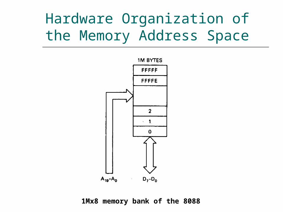
Hardware Organization of the Memory Address Space (cont)
Odd address byte transfer by the 8086
Hardware Organization of the Memory Address Space (cont)
Even address word transfer by the 8086
Hardware Organization of the Memory Address Space (cont)
Odd-address word transfer by the 8086
Hardware Organization of the Memory Address Space (cont)
EXAMPLE Is the word at memory address 0123116 of an
8086-based microcomputer aligned or misaligned How many cycle are required to read it from memory
Solution The first byte of the word is the second byte at
the aligned-word address 0123016 Therefore the word is misaligned and required two bus cycles to be read from memory
Address Bus Status Codes
Whenever a memory bus cycle is in progress an address bus status code S4S3 is output by the processor S4S3 identifies which one of the four segment
register is used to generate the physical address in the current bus cycle 1048729
S4S3=00 identifies the extra segment register (ES)
S4S3=01 identifies the stack segment register (SS)
S4S3=10 identifies the code segment register (CS)
S4S3=11 identifies the data segment register (DS)
The memory address reach of the microprocessor can thus be expanded to 4 Mbytes
Memory Control Signals
Minimum-mode memory control signals
Memory Control Signals (cont)
Minimum-mode memory control signals (8088) ALE ndash Address Latch Enable ndash used to latch
the address in external memory IOM ndash Input-OutputMemory ndash signal external
circuitry whether a memory of IO bus cycle is in progress
DTR ndash Data TransmitReceive ndash signal external circuitry whether the 8088 is transmitting or receiving data over the bus 1048729
RD ndash Read ndash identifies that a read bus cycle is in progress
WR ndash Write ndash identifies that a write bus cycle is in progress
DEN ndash Data Enable ndash used to enable the data bus 1048729
SSO ndash Status Line ndash identifies whether a code or data access is in progress
Memory Control Signals (cont)
The control signals for the 8086rsquos minimum-mode memory interface differs in three ways IOM signal is replaced by MIO signal The signal SSO is removed from the interface BHE (bank high enable) is added to the interface
and is used to select input for the high bank of memory in the 8086rsquos memory subsystem
Memory Control Signals (cont)
Maximum-mode memory control signals
Memory Control Signals (cont)
Maximum-mode memory control signals MRDC ndash Memory Read Command 1048729 MWTC ndash Memory Write Command 1048729 AMWC ndash Advanced Memory Write Command
Read and Write Bus Cycle
Read cycle
Minimum-mode memory read bus cycle of the 8088
Read and Write Bus Cycle (cont)
Read cycle
Minimum-mode memory read bus cycle of the 8086
Read and Write Bus Cycle (cont)
Read cycle
Maximum-mode memory read bus cycle of the 8086
Read and Write Bus Cycle (cont)
Write cycle
Minimum-mode memory write bus cycle of the 8088
Read and Write Bus Cycle (cont)
Write cycle
Maximum-mode memory write bus cycle of the 8086
Memory Interface Circuit
Address bus latches and buffers Bank write and bank read control logic Data bus transceiversbuffers Address decoders
Memory Interface Circuit (cont)
Memory interface block diagram
Memory Interface Circuit (cont)
Address bus latches and buffers
Block diagram of a D-type latch
Memory Interface Circuit (cont)
Address bus latches and buffers
Circuit diagram of the 74F373
Memory Interface Circuit (cont)
A review of flip-floplatch logic
Positive edge-triggered D flip-flop
Memory Interface Circuit (cont)
A review of flip-floplatch logic
Positive edge-triggered JK flip-flop
Memory Interface Circuit (cont)
A review of flip-floplatch logic
D-type latch
Memory Interface Circuit (cont)
Address bus latches and buffers
Address latch circuit
Memory Interface Circuit (cont)
Bank write and bank read control logic
Bank write control logic Bank read control logic
Memory Interface Circuit (cont)
Data bus transceivers
Block diagram and circuit diagram of the 74F245 octal bus transceiver
Memory Interface Circuit (cont)
Data bus transceivers
Data bus transceiver circuit
Memory Interface Circuit (cont)
Address decoder
Address bus configuration with address decoding
Memory Interface Circuit (cont)
Address decoder
Block diagram and operation of the 74F139 decoder
Memory Interface Circuit (cont)
Address decoder
Circuit diagram of the 74F139 decoder
Memory Interface Circuit (cont)
Address decoder
Address decoder circuit using 74F139
Memory Interface Circuit (cont)
Address decoder
Block diagram and operation of the 74F138 decoder
Memory Interface Circuit (cont)
Address decoder
Circuit diagram of the 74F138 decoder
Memory Interface Circuit (cont)
Address decoder
Address decoder circuit using 74F138
Types of InputOutput
The IO system allows peripherals to provide data or receive results of processing the data Using IO ports
The 80888086 MPU can employ two types of IO Isolated IO Memory-mapped IO
They differ in how IO ports are mapped into the address space
Types of InputOutput (cont)
Isolated inputoutput When using isolated IO in a microcomputer
system the IO device are treated separate from memory
The memory address space contains 1 M consecutive byte address in the range 0000016 through FFFFF16
The IO address space contains 64K consecutive byte addresses in the range 000016 through FFFF16
The bytes in two consecutive IO addresses can be accessed as word-wide data
Page 0 000016 00FF16
Certain IO instructions can only perform in this range
Types of InputOutput (cont)
Isolated inputoutput
80888086 memory and IO address spaces
Types of InputOutput (cont)
Isolated inputoutput
Isolated IO ports
Types of InputOutput (cont)
Isolated inputoutput Advantages
The complete 1Mbyte memory address space is available for use with memory
Special instructions have been provided to perform IO operations with maximized performance
The bytes in two consecutive IO addresses can be accessed as word-wide data
Disadvantages All input and output data transfers must take place
between the AL or AX register and IO port
Types of InputOutput (cont)
Memory-mapped inputoutput MPU looks at the IO port as though it is a storage
location in memory Some of the memory address space is dedicated to IO
ports Instructions that affect data in memory are used
instead of the special IO instructions More instructions and addressing modes are available to
perform IO operations IO transfers can take place between IO port and other
internal registers The memory instructions tend to execute slower
than those specifically designed for isolated IO Part of the memory address space is lost
Types of InputOutput(cont)
Memory-mapped inputoutput
Memory mapped IO ports
Isolated InputOutput Interface
IO devices Keyboard Printer Mouse 82C55A etc
Functions of interface circuit Select the IO port Latch output data Sample input data Synchronize data transfer Translate between TTL voltage levels and those
required to operate the IO devices
Isolated InputOutput Interface (cont)
Minimum-mode interface
Minimum-mode 8088 system IO interface
Isolated InputOutput Interface (cont)
Minimum-mode interface
Minimum-mode 8086 system IO interface
Isolated InputOutput Interface (cont)
Maximum-mode interface
Maximum-mode 8088 system IO interface
Isolated InputOutput Interface (cont)
Maximum-mode interface
Maximum-mode 8086 system IO interface
Isolated InputOutput Interface (cont)
Maximum-mode interface
IO bus cycle status codes
InputOutput Data Transfer
Inputoutput data transfers in the 8088 and 8086 microcomputers can be either byte-wide or word-wide
IO addresses are 16 bits in length and are output by the 8088 to the IO interface over bus lines AD0 through AD7 and A8 through A15
In 8088 the word transfers is performed as two consecutive byte-wide data transfer and takes two bus cycle
In 8086 the word transfers can takes either one or two bus cycle
Word-wide IO ports should be aligned at even-address boundaries
InputOutput Data Instructions
InputOutput Data Instructions(cont)
EXAMPLE Write a sequence of instructions that will output
the data FF16 to a byte-wide output port at address AB16 of the IO address space
Solution First the AL register is loaded with FF16 as an
immediate operand in the instruction
MOV AL 0FFH Now the data in AL can be output to the byte-
wide output port with the instruction
OUT 0ABH AL
InputOutput Data Instructions(cont)
EXAMPLE Write a series of instructions that will output FF16 to an
output port located at address B00016 of the IO address space
Solution The DX register must first be loaded with the address
of the output port This is done with the instructionMOV DX 0B000H
Next the data that are to be output must be loaded into AL with the instruction
MOV AL 0FFH Finally the data are output with the instruction
OUT DX AL
InputOutput Data Instructions(cont)
EXAMPLE Data are to be read in from two byte-wide input
ports at addresses AA16 and A916 and then output as a word-wide output port at address B00016 Write a sequence of instructions to perform this inputoutput operation
InputOutput Data Instructions(cont)
Solution First read in the byte at address AA16 into AL and
move it into AHIN AL 0AAHMOV AH AL
Now the other byte can be read into AL by the instructionIN AL 09AH
And to write out the word of dataMOV DX 0B000HOUT DX AX
InputOutput Bus Cycles
Input bus cycle of the 8088
InputOutput Bus Cycles (cont)
Output bus cycle of the 8088
InputOutput Bus Cycles (cont)
Input bus cycle of the 8086
InputOutput Bus Cycles (cont)
Output bus cycle of the 8086
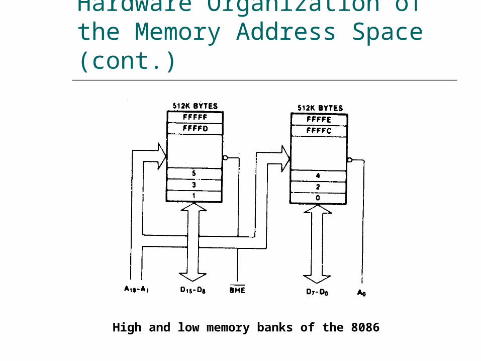
Hardware Organization of the Memory Address Space (cont)
Odd-address word transfer by the 8086
Hardware Organization of the Memory Address Space (cont)
EXAMPLE Is the word at memory address 0123116 of an
8086-based microcomputer aligned or misaligned How many cycle are required to read it from memory
Solution The first byte of the word is the second byte at
the aligned-word address 0123016 Therefore the word is misaligned and required two bus cycles to be read from memory
Address Bus Status Codes
Whenever a memory bus cycle is in progress an address bus status code S4S3 is output by the processor S4S3 identifies which one of the four segment
register is used to generate the physical address in the current bus cycle 1048729
S4S3=00 identifies the extra segment register (ES)
S4S3=01 identifies the stack segment register (SS)
S4S3=10 identifies the code segment register (CS)
S4S3=11 identifies the data segment register (DS)
The memory address reach of the microprocessor can thus be expanded to 4 Mbytes
Memory Control Signals
Minimum-mode memory control signals
Memory Control Signals (cont)
Minimum-mode memory control signals (8088) ALE ndash Address Latch Enable ndash used to latch
the address in external memory IOM ndash Input-OutputMemory ndash signal external
circuitry whether a memory of IO bus cycle is in progress
DTR ndash Data TransmitReceive ndash signal external circuitry whether the 8088 is transmitting or receiving data over the bus 1048729
RD ndash Read ndash identifies that a read bus cycle is in progress
WR ndash Write ndash identifies that a write bus cycle is in progress
DEN ndash Data Enable ndash used to enable the data bus 1048729
SSO ndash Status Line ndash identifies whether a code or data access is in progress
Memory Control Signals (cont)
The control signals for the 8086rsquos minimum-mode memory interface differs in three ways IOM signal is replaced by MIO signal The signal SSO is removed from the interface BHE (bank high enable) is added to the interface
and is used to select input for the high bank of memory in the 8086rsquos memory subsystem
Memory Control Signals (cont)
Maximum-mode memory control signals
Memory Control Signals (cont)
Maximum-mode memory control signals MRDC ndash Memory Read Command 1048729 MWTC ndash Memory Write Command 1048729 AMWC ndash Advanced Memory Write Command
Read and Write Bus Cycle
Read cycle
Minimum-mode memory read bus cycle of the 8088
Read and Write Bus Cycle (cont)
Read cycle
Minimum-mode memory read bus cycle of the 8086
Read and Write Bus Cycle (cont)
Read cycle
Maximum-mode memory read bus cycle of the 8086
Read and Write Bus Cycle (cont)
Write cycle
Minimum-mode memory write bus cycle of the 8088
Read and Write Bus Cycle (cont)
Write cycle
Maximum-mode memory write bus cycle of the 8086
Memory Interface Circuit
Address bus latches and buffers Bank write and bank read control logic Data bus transceiversbuffers Address decoders
Memory Interface Circuit (cont)
Memory interface block diagram
Memory Interface Circuit (cont)
Address bus latches and buffers
Block diagram of a D-type latch
Memory Interface Circuit (cont)
Address bus latches and buffers
Circuit diagram of the 74F373
Memory Interface Circuit (cont)
A review of flip-floplatch logic
Positive edge-triggered D flip-flop
Memory Interface Circuit (cont)
A review of flip-floplatch logic
Positive edge-triggered JK flip-flop
Memory Interface Circuit (cont)
A review of flip-floplatch logic
D-type latch
Memory Interface Circuit (cont)
Address bus latches and buffers
Address latch circuit
Memory Interface Circuit (cont)
Bank write and bank read control logic
Bank write control logic Bank read control logic
Memory Interface Circuit (cont)
Data bus transceivers
Block diagram and circuit diagram of the 74F245 octal bus transceiver
Memory Interface Circuit (cont)
Data bus transceivers
Data bus transceiver circuit
Memory Interface Circuit (cont)
Address decoder
Address bus configuration with address decoding
Memory Interface Circuit (cont)
Address decoder
Block diagram and operation of the 74F139 decoder
Memory Interface Circuit (cont)
Address decoder
Circuit diagram of the 74F139 decoder
Memory Interface Circuit (cont)
Address decoder
Address decoder circuit using 74F139
Memory Interface Circuit (cont)
Address decoder
Block diagram and operation of the 74F138 decoder
Memory Interface Circuit (cont)
Address decoder
Circuit diagram of the 74F138 decoder
Memory Interface Circuit (cont)
Address decoder
Address decoder circuit using 74F138
Types of InputOutput
The IO system allows peripherals to provide data or receive results of processing the data Using IO ports
The 80888086 MPU can employ two types of IO Isolated IO Memory-mapped IO
They differ in how IO ports are mapped into the address space
Types of InputOutput (cont)
Isolated inputoutput When using isolated IO in a microcomputer
system the IO device are treated separate from memory
The memory address space contains 1 M consecutive byte address in the range 0000016 through FFFFF16
The IO address space contains 64K consecutive byte addresses in the range 000016 through FFFF16
The bytes in two consecutive IO addresses can be accessed as word-wide data
Page 0 000016 00FF16
Certain IO instructions can only perform in this range
Types of InputOutput (cont)
Isolated inputoutput
80888086 memory and IO address spaces
Types of InputOutput (cont)
Isolated inputoutput
Isolated IO ports
Types of InputOutput (cont)
Isolated inputoutput Advantages
The complete 1Mbyte memory address space is available for use with memory
Special instructions have been provided to perform IO operations with maximized performance
The bytes in two consecutive IO addresses can be accessed as word-wide data
Disadvantages All input and output data transfers must take place
between the AL or AX register and IO port
Types of InputOutput (cont)
Memory-mapped inputoutput MPU looks at the IO port as though it is a storage
location in memory Some of the memory address space is dedicated to IO
ports Instructions that affect data in memory are used
instead of the special IO instructions More instructions and addressing modes are available to
perform IO operations IO transfers can take place between IO port and other
internal registers The memory instructions tend to execute slower
than those specifically designed for isolated IO Part of the memory address space is lost
Types of InputOutput(cont)
Memory-mapped inputoutput
Memory mapped IO ports
Isolated InputOutput Interface
IO devices Keyboard Printer Mouse 82C55A etc
Functions of interface circuit Select the IO port Latch output data Sample input data Synchronize data transfer Translate between TTL voltage levels and those
required to operate the IO devices
Isolated InputOutput Interface (cont)
Minimum-mode interface
Minimum-mode 8088 system IO interface
Isolated InputOutput Interface (cont)
Minimum-mode interface
Minimum-mode 8086 system IO interface
Isolated InputOutput Interface (cont)
Maximum-mode interface
Maximum-mode 8088 system IO interface
Isolated InputOutput Interface (cont)
Maximum-mode interface
Maximum-mode 8086 system IO interface
Isolated InputOutput Interface (cont)
Maximum-mode interface
IO bus cycle status codes
InputOutput Data Transfer
Inputoutput data transfers in the 8088 and 8086 microcomputers can be either byte-wide or word-wide
IO addresses are 16 bits in length and are output by the 8088 to the IO interface over bus lines AD0 through AD7 and A8 through A15
In 8088 the word transfers is performed as two consecutive byte-wide data transfer and takes two bus cycle
In 8086 the word transfers can takes either one or two bus cycle
Word-wide IO ports should be aligned at even-address boundaries
InputOutput Data Instructions
InputOutput Data Instructions(cont)
EXAMPLE Write a sequence of instructions that will output
the data FF16 to a byte-wide output port at address AB16 of the IO address space
Solution First the AL register is loaded with FF16 as an
immediate operand in the instruction
MOV AL 0FFH Now the data in AL can be output to the byte-
wide output port with the instruction
OUT 0ABH AL
InputOutput Data Instructions(cont)
EXAMPLE Write a series of instructions that will output FF16 to an
output port located at address B00016 of the IO address space
Solution The DX register must first be loaded with the address
of the output port This is done with the instructionMOV DX 0B000H
Next the data that are to be output must be loaded into AL with the instruction
MOV AL 0FFH Finally the data are output with the instruction
OUT DX AL
InputOutput Data Instructions(cont)
EXAMPLE Data are to be read in from two byte-wide input
ports at addresses AA16 and A916 and then output as a word-wide output port at address B00016 Write a sequence of instructions to perform this inputoutput operation
InputOutput Data Instructions(cont)
Solution First read in the byte at address AA16 into AL and
move it into AHIN AL 0AAHMOV AH AL
Now the other byte can be read into AL by the instructionIN AL 09AH
And to write out the word of dataMOV DX 0B000HOUT DX AX
InputOutput Bus Cycles
Input bus cycle of the 8088
InputOutput Bus Cycles (cont)
Output bus cycle of the 8088
InputOutput Bus Cycles (cont)
Input bus cycle of the 8086
InputOutput Bus Cycles (cont)
Output bus cycle of the 8086
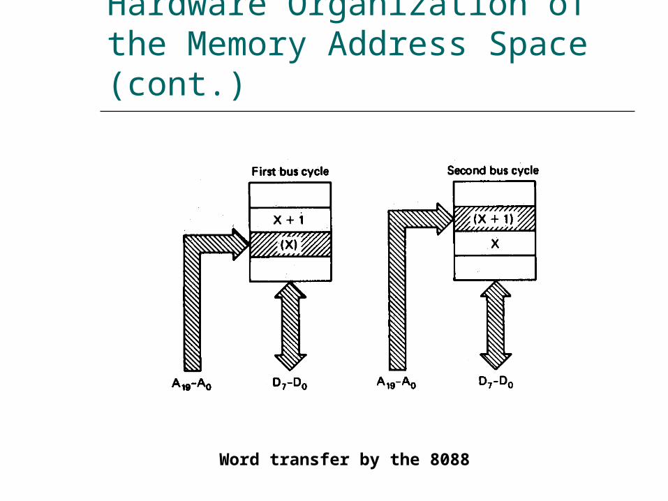
Hardware Organization of the Memory Address Space (cont)
EXAMPLE Is the word at memory address 0123116 of an
8086-based microcomputer aligned or misaligned How many cycle are required to read it from memory
Solution The first byte of the word is the second byte at
the aligned-word address 0123016 Therefore the word is misaligned and required two bus cycles to be read from memory
Address Bus Status Codes
Whenever a memory bus cycle is in progress an address bus status code S4S3 is output by the processor S4S3 identifies which one of the four segment
register is used to generate the physical address in the current bus cycle 1048729
S4S3=00 identifies the extra segment register (ES)
S4S3=01 identifies the stack segment register (SS)
S4S3=10 identifies the code segment register (CS)
S4S3=11 identifies the data segment register (DS)
The memory address reach of the microprocessor can thus be expanded to 4 Mbytes
Memory Control Signals
Minimum-mode memory control signals
Memory Control Signals (cont)
Minimum-mode memory control signals (8088) ALE ndash Address Latch Enable ndash used to latch
the address in external memory IOM ndash Input-OutputMemory ndash signal external
circuitry whether a memory of IO bus cycle is in progress
DTR ndash Data TransmitReceive ndash signal external circuitry whether the 8088 is transmitting or receiving data over the bus 1048729
RD ndash Read ndash identifies that a read bus cycle is in progress
WR ndash Write ndash identifies that a write bus cycle is in progress
DEN ndash Data Enable ndash used to enable the data bus 1048729
SSO ndash Status Line ndash identifies whether a code or data access is in progress
Memory Control Signals (cont)
The control signals for the 8086rsquos minimum-mode memory interface differs in three ways IOM signal is replaced by MIO signal The signal SSO is removed from the interface BHE (bank high enable) is added to the interface
and is used to select input for the high bank of memory in the 8086rsquos memory subsystem
Memory Control Signals (cont)
Maximum-mode memory control signals
Memory Control Signals (cont)
Maximum-mode memory control signals MRDC ndash Memory Read Command 1048729 MWTC ndash Memory Write Command 1048729 AMWC ndash Advanced Memory Write Command
Read and Write Bus Cycle
Read cycle
Minimum-mode memory read bus cycle of the 8088
Read and Write Bus Cycle (cont)
Read cycle
Minimum-mode memory read bus cycle of the 8086
Read and Write Bus Cycle (cont)
Read cycle
Maximum-mode memory read bus cycle of the 8086
Read and Write Bus Cycle (cont)
Write cycle
Minimum-mode memory write bus cycle of the 8088
Read and Write Bus Cycle (cont)
Write cycle
Maximum-mode memory write bus cycle of the 8086
Memory Interface Circuit
Address bus latches and buffers Bank write and bank read control logic Data bus transceiversbuffers Address decoders
Memory Interface Circuit (cont)
Memory interface block diagram
Memory Interface Circuit (cont)
Address bus latches and buffers
Block diagram of a D-type latch
Memory Interface Circuit (cont)
Address bus latches and buffers
Circuit diagram of the 74F373
Memory Interface Circuit (cont)
A review of flip-floplatch logic
Positive edge-triggered D flip-flop
Memory Interface Circuit (cont)
A review of flip-floplatch logic
Positive edge-triggered JK flip-flop
Memory Interface Circuit (cont)
A review of flip-floplatch logic
D-type latch
Memory Interface Circuit (cont)
Address bus latches and buffers
Address latch circuit
Memory Interface Circuit (cont)
Bank write and bank read control logic
Bank write control logic Bank read control logic
Memory Interface Circuit (cont)
Data bus transceivers
Block diagram and circuit diagram of the 74F245 octal bus transceiver
Memory Interface Circuit (cont)
Data bus transceivers
Data bus transceiver circuit
Memory Interface Circuit (cont)
Address decoder
Address bus configuration with address decoding
Memory Interface Circuit (cont)
Address decoder
Block diagram and operation of the 74F139 decoder
Memory Interface Circuit (cont)
Address decoder
Circuit diagram of the 74F139 decoder
Memory Interface Circuit (cont)
Address decoder
Address decoder circuit using 74F139
Memory Interface Circuit (cont)
Address decoder
Block diagram and operation of the 74F138 decoder
Memory Interface Circuit (cont)
Address decoder
Circuit diagram of the 74F138 decoder
Memory Interface Circuit (cont)
Address decoder
Address decoder circuit using 74F138
Types of InputOutput
The IO system allows peripherals to provide data or receive results of processing the data Using IO ports
The 80888086 MPU can employ two types of IO Isolated IO Memory-mapped IO
They differ in how IO ports are mapped into the address space
Types of InputOutput (cont)
Isolated inputoutput When using isolated IO in a microcomputer
system the IO device are treated separate from memory
The memory address space contains 1 M consecutive byte address in the range 0000016 through FFFFF16
The IO address space contains 64K consecutive byte addresses in the range 000016 through FFFF16
The bytes in two consecutive IO addresses can be accessed as word-wide data
Page 0 000016 00FF16
Certain IO instructions can only perform in this range
Types of InputOutput (cont)
Isolated inputoutput
80888086 memory and IO address spaces
Types of InputOutput (cont)
Isolated inputoutput
Isolated IO ports
Types of InputOutput (cont)
Isolated inputoutput Advantages
The complete 1Mbyte memory address space is available for use with memory
Special instructions have been provided to perform IO operations with maximized performance
The bytes in two consecutive IO addresses can be accessed as word-wide data
Disadvantages All input and output data transfers must take place
between the AL or AX register and IO port
Types of InputOutput (cont)
Memory-mapped inputoutput MPU looks at the IO port as though it is a storage
location in memory Some of the memory address space is dedicated to IO
ports Instructions that affect data in memory are used
instead of the special IO instructions More instructions and addressing modes are available to
perform IO operations IO transfers can take place between IO port and other
internal registers The memory instructions tend to execute slower
than those specifically designed for isolated IO Part of the memory address space is lost
Types of InputOutput(cont)
Memory-mapped inputoutput
Memory mapped IO ports
Isolated InputOutput Interface
IO devices Keyboard Printer Mouse 82C55A etc
Functions of interface circuit Select the IO port Latch output data Sample input data Synchronize data transfer Translate between TTL voltage levels and those
required to operate the IO devices
Isolated InputOutput Interface (cont)
Minimum-mode interface
Minimum-mode 8088 system IO interface
Isolated InputOutput Interface (cont)
Minimum-mode interface
Minimum-mode 8086 system IO interface
Isolated InputOutput Interface (cont)
Maximum-mode interface
Maximum-mode 8088 system IO interface
Isolated InputOutput Interface (cont)
Maximum-mode interface
Maximum-mode 8086 system IO interface
Isolated InputOutput Interface (cont)
Maximum-mode interface
IO bus cycle status codes
InputOutput Data Transfer
Inputoutput data transfers in the 8088 and 8086 microcomputers can be either byte-wide or word-wide
IO addresses are 16 bits in length and are output by the 8088 to the IO interface over bus lines AD0 through AD7 and A8 through A15
In 8088 the word transfers is performed as two consecutive byte-wide data transfer and takes two bus cycle
In 8086 the word transfers can takes either one or two bus cycle
Word-wide IO ports should be aligned at even-address boundaries
InputOutput Data Instructions
InputOutput Data Instructions(cont)
EXAMPLE Write a sequence of instructions that will output
the data FF16 to a byte-wide output port at address AB16 of the IO address space
Solution First the AL register is loaded with FF16 as an
immediate operand in the instruction
MOV AL 0FFH Now the data in AL can be output to the byte-
wide output port with the instruction
OUT 0ABH AL
InputOutput Data Instructions(cont)
EXAMPLE Write a series of instructions that will output FF16 to an
output port located at address B00016 of the IO address space
Solution The DX register must first be loaded with the address
of the output port This is done with the instructionMOV DX 0B000H
Next the data that are to be output must be loaded into AL with the instruction
MOV AL 0FFH Finally the data are output with the instruction
OUT DX AL
InputOutput Data Instructions(cont)
EXAMPLE Data are to be read in from two byte-wide input
ports at addresses AA16 and A916 and then output as a word-wide output port at address B00016 Write a sequence of instructions to perform this inputoutput operation
InputOutput Data Instructions(cont)
Solution First read in the byte at address AA16 into AL and
move it into AHIN AL 0AAHMOV AH AL
Now the other byte can be read into AL by the instructionIN AL 09AH
And to write out the word of dataMOV DX 0B000HOUT DX AX
InputOutput Bus Cycles
Input bus cycle of the 8088
InputOutput Bus Cycles (cont)
Output bus cycle of the 8088
InputOutput Bus Cycles (cont)
Input bus cycle of the 8086
InputOutput Bus Cycles (cont)
Output bus cycle of the 8086
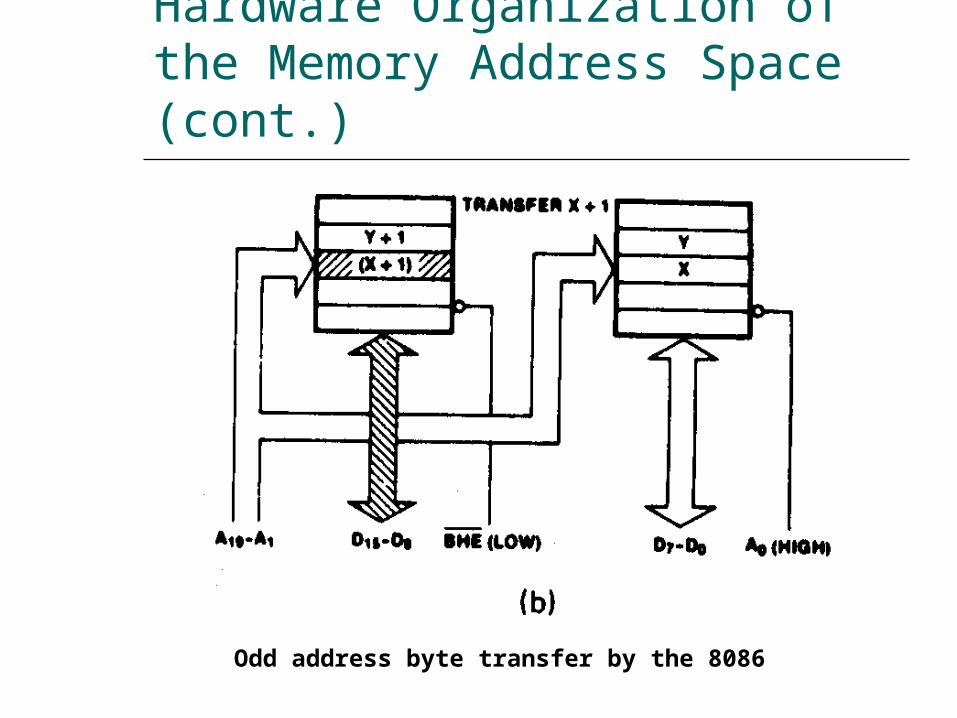
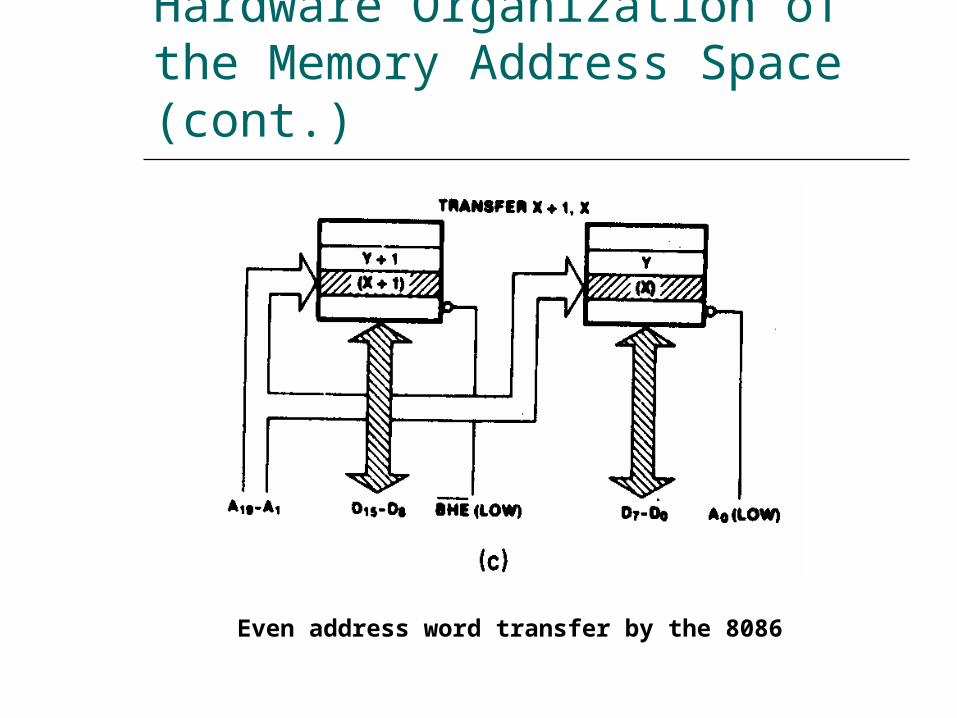
Memory Control Signals (cont)
Maximum-mode memory control signals
Memory Control Signals (cont)
Maximum-mode memory control signals MRDC ndash Memory Read Command 1048729 MWTC ndash Memory Write Command 1048729 AMWC ndash Advanced Memory Write Command
Read and Write Bus Cycle
Read cycle
Minimum-mode memory read bus cycle of the 8088
Read and Write Bus Cycle (cont)
Read cycle
Minimum-mode memory read bus cycle of the 8086
Read and Write Bus Cycle (cont)
Read cycle
Maximum-mode memory read bus cycle of the 8086
Read and Write Bus Cycle (cont)
Write cycle
Minimum-mode memory write bus cycle of the 8088
Read and Write Bus Cycle (cont)
Write cycle
Maximum-mode memory write bus cycle of the 8086
Memory Interface Circuit
Address bus latches and buffers Bank write and bank read control logic Data bus transceiversbuffers Address decoders
Memory Interface Circuit (cont)
Memory interface block diagram
Memory Interface Circuit (cont)
Address bus latches and buffers
Block diagram of a D-type latch
Memory Interface Circuit (cont)
Address bus latches and buffers
Circuit diagram of the 74F373
Memory Interface Circuit (cont)
A review of flip-floplatch logic
Positive edge-triggered D flip-flop
Memory Interface Circuit (cont)
A review of flip-floplatch logic
Positive edge-triggered JK flip-flop
Memory Interface Circuit (cont)
A review of flip-floplatch logic
D-type latch
Memory Interface Circuit (cont)
Address bus latches and buffers
Address latch circuit
Memory Interface Circuit (cont)
Bank write and bank read control logic
Bank write control logic Bank read control logic
Memory Interface Circuit (cont)
Data bus transceivers
Block diagram and circuit diagram of the 74F245 octal bus transceiver
Memory Interface Circuit (cont)
Data bus transceivers
Data bus transceiver circuit
Memory Interface Circuit (cont)
Address decoder
Address bus configuration with address decoding
Memory Interface Circuit (cont)
Address decoder
Block diagram and operation of the 74F139 decoder
Memory Interface Circuit (cont)
Address decoder
Circuit diagram of the 74F139 decoder
Memory Interface Circuit (cont)
Address decoder
Address decoder circuit using 74F139
Memory Interface Circuit (cont)
Address decoder
Block diagram and operation of the 74F138 decoder
Memory Interface Circuit (cont)
Address decoder
Circuit diagram of the 74F138 decoder
Memory Interface Circuit (cont)
Address decoder
Address decoder circuit using 74F138
Types of InputOutput
The IO system allows peripherals to provide data or receive results of processing the data Using IO ports
The 80888086 MPU can employ two types of IO Isolated IO Memory-mapped IO
They differ in how IO ports are mapped into the address space
Types of InputOutput (cont)
Isolated inputoutput When using isolated IO in a microcomputer
system the IO device are treated separate from memory
The memory address space contains 1 M consecutive byte address in the range 0000016 through FFFFF16
The IO address space contains 64K consecutive byte addresses in the range 000016 through FFFF16
The bytes in two consecutive IO addresses can be accessed as word-wide data
Page 0 000016 00FF16
Certain IO instructions can only perform in this range
Types of InputOutput (cont)
Isolated inputoutput
80888086 memory and IO address spaces
Types of InputOutput (cont)
Isolated inputoutput
Isolated IO ports
Types of InputOutput (cont)
Isolated inputoutput Advantages
The complete 1Mbyte memory address space is available for use with memory
Special instructions have been provided to perform IO operations with maximized performance
The bytes in two consecutive IO addresses can be accessed as word-wide data
Disadvantages All input and output data transfers must take place
between the AL or AX register and IO port
Types of InputOutput (cont)
Memory-mapped inputoutput MPU looks at the IO port as though it is a storage
location in memory Some of the memory address space is dedicated to IO
ports Instructions that affect data in memory are used
instead of the special IO instructions More instructions and addressing modes are available to
perform IO operations IO transfers can take place between IO port and other
internal registers The memory instructions tend to execute slower
than those specifically designed for isolated IO Part of the memory address space is lost
Types of InputOutput(cont)
Memory-mapped inputoutput
Memory mapped IO ports
Isolated InputOutput Interface
IO devices Keyboard Printer Mouse 82C55A etc
Functions of interface circuit Select the IO port Latch output data Sample input data Synchronize data transfer Translate between TTL voltage levels and those
required to operate the IO devices
Isolated InputOutput Interface (cont)
Minimum-mode interface
Minimum-mode 8088 system IO interface
Isolated InputOutput Interface (cont)
Minimum-mode interface
Minimum-mode 8086 system IO interface
Isolated InputOutput Interface (cont)
Maximum-mode interface
Maximum-mode 8088 system IO interface
Isolated InputOutput Interface (cont)
Maximum-mode interface
Maximum-mode 8086 system IO interface
Isolated InputOutput Interface (cont)
Maximum-mode interface
IO bus cycle status codes
InputOutput Data Transfer
Inputoutput data transfers in the 8088 and 8086 microcomputers can be either byte-wide or word-wide
IO addresses are 16 bits in length and are output by the 8088 to the IO interface over bus lines AD0 through AD7 and A8 through A15
In 8088 the word transfers is performed as two consecutive byte-wide data transfer and takes two bus cycle
In 8086 the word transfers can takes either one or two bus cycle
Word-wide IO ports should be aligned at even-address boundaries
InputOutput Data Instructions
InputOutput Data Instructions(cont)
EXAMPLE Write a sequence of instructions that will output
the data FF16 to a byte-wide output port at address AB16 of the IO address space
Solution First the AL register is loaded with FF16 as an
immediate operand in the instruction
MOV AL 0FFH Now the data in AL can be output to the byte-
wide output port with the instruction
OUT 0ABH AL
InputOutput Data Instructions(cont)
EXAMPLE Write a series of instructions that will output FF16 to an
output port located at address B00016 of the IO address space
Solution The DX register must first be loaded with the address
of the output port This is done with the instructionMOV DX 0B000H
Next the data that are to be output must be loaded into AL with the instruction
MOV AL 0FFH Finally the data are output with the instruction
OUT DX AL
InputOutput Data Instructions(cont)
EXAMPLE Data are to be read in from two byte-wide input
ports at addresses AA16 and A916 and then output as a word-wide output port at address B00016 Write a sequence of instructions to perform this inputoutput operation
InputOutput Data Instructions(cont)
Solution First read in the byte at address AA16 into AL and
move it into AHIN AL 0AAHMOV AH AL
Now the other byte can be read into AL by the instructionIN AL 09AH
And to write out the word of dataMOV DX 0B000HOUT DX AX
InputOutput Bus Cycles
Input bus cycle of the 8088
InputOutput Bus Cycles (cont)
Output bus cycle of the 8088
InputOutput Bus Cycles (cont)
Input bus cycle of the 8086
InputOutput Bus Cycles (cont)
Output bus cycle of the 8086
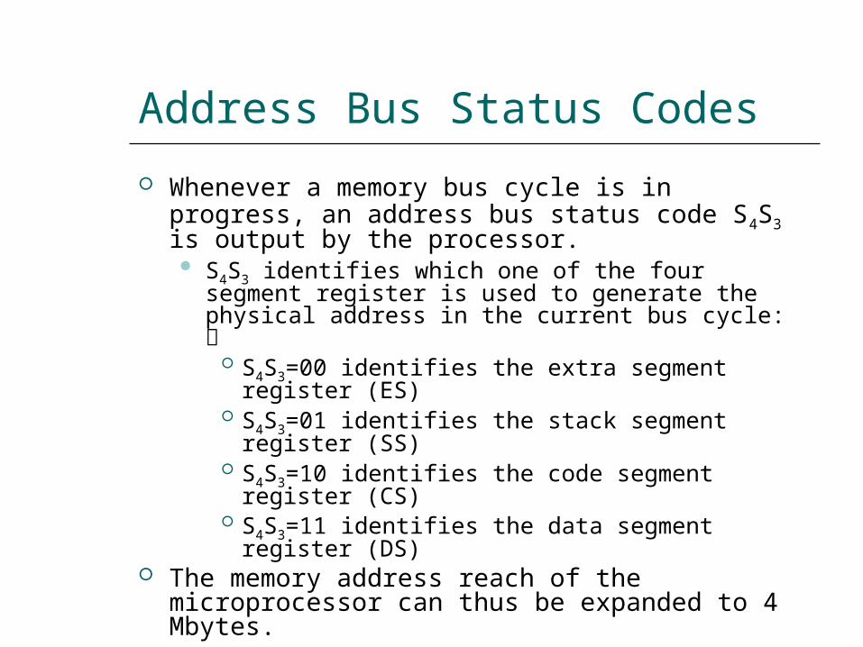
Memory Control Signals (cont)
Maximum-mode memory control signals MRDC ndash Memory Read Command 1048729 MWTC ndash Memory Write Command 1048729 AMWC ndash Advanced Memory Write Command
Read and Write Bus Cycle
Read cycle
Minimum-mode memory read bus cycle of the 8088
Read and Write Bus Cycle (cont)
Read cycle
Minimum-mode memory read bus cycle of the 8086
Read and Write Bus Cycle (cont)
Read cycle
Maximum-mode memory read bus cycle of the 8086
Read and Write Bus Cycle (cont)
Write cycle
Minimum-mode memory write bus cycle of the 8088
Read and Write Bus Cycle (cont)
Write cycle
Maximum-mode memory write bus cycle of the 8086
Memory Interface Circuit
Address bus latches and buffers Bank write and bank read control logic Data bus transceiversbuffers Address decoders
Memory Interface Circuit (cont)
Memory interface block diagram
Memory Interface Circuit (cont)
Address bus latches and buffers
Block diagram of a D-type latch
Memory Interface Circuit (cont)
Address bus latches and buffers
Circuit diagram of the 74F373
Memory Interface Circuit (cont)
A review of flip-floplatch logic
Positive edge-triggered D flip-flop
Memory Interface Circuit (cont)
A review of flip-floplatch logic
Positive edge-triggered JK flip-flop
Memory Interface Circuit (cont)
A review of flip-floplatch logic
D-type latch
Memory Interface Circuit (cont)
Address bus latches and buffers
Address latch circuit
Memory Interface Circuit (cont)
Bank write and bank read control logic
Bank write control logic Bank read control logic
Memory Interface Circuit (cont)
Data bus transceivers
Block diagram and circuit diagram of the 74F245 octal bus transceiver
Memory Interface Circuit (cont)
Data bus transceivers
Data bus transceiver circuit
Memory Interface Circuit (cont)
Address decoder
Address bus configuration with address decoding
Memory Interface Circuit (cont)
Address decoder
Block diagram and operation of the 74F139 decoder
Memory Interface Circuit (cont)
Address decoder
Circuit diagram of the 74F139 decoder
Memory Interface Circuit (cont)
Address decoder
Address decoder circuit using 74F139
Memory Interface Circuit (cont)
Address decoder
Block diagram and operation of the 74F138 decoder
Memory Interface Circuit (cont)
Address decoder
Circuit diagram of the 74F138 decoder
Memory Interface Circuit (cont)
Address decoder
Address decoder circuit using 74F138
Types of InputOutput
The IO system allows peripherals to provide data or receive results of processing the data Using IO ports
The 80888086 MPU can employ two types of IO Isolated IO Memory-mapped IO
They differ in how IO ports are mapped into the address space
Types of InputOutput (cont)
Isolated inputoutput When using isolated IO in a microcomputer
system the IO device are treated separate from memory
The memory address space contains 1 M consecutive byte address in the range 0000016 through FFFFF16
The IO address space contains 64K consecutive byte addresses in the range 000016 through FFFF16
The bytes in two consecutive IO addresses can be accessed as word-wide data
Page 0 000016 00FF16
Certain IO instructions can only perform in this range
Types of InputOutput (cont)
Isolated inputoutput
80888086 memory and IO address spaces
Types of InputOutput (cont)
Isolated inputoutput
Isolated IO ports
Types of InputOutput (cont)
Isolated inputoutput Advantages
The complete 1Mbyte memory address space is available for use with memory
Special instructions have been provided to perform IO operations with maximized performance
The bytes in two consecutive IO addresses can be accessed as word-wide data
Disadvantages All input and output data transfers must take place
between the AL or AX register and IO port
Types of InputOutput (cont)
Memory-mapped inputoutput MPU looks at the IO port as though it is a storage
location in memory Some of the memory address space is dedicated to IO
ports Instructions that affect data in memory are used
instead of the special IO instructions More instructions and addressing modes are available to
perform IO operations IO transfers can take place between IO port and other
internal registers The memory instructions tend to execute slower
than those specifically designed for isolated IO Part of the memory address space is lost
Types of InputOutput(cont)
Memory-mapped inputoutput
Memory mapped IO ports
Isolated InputOutput Interface
IO devices Keyboard Printer Mouse 82C55A etc
Functions of interface circuit Select the IO port Latch output data Sample input data Synchronize data transfer Translate between TTL voltage levels and those
required to operate the IO devices
Isolated InputOutput Interface (cont)
Minimum-mode interface
Minimum-mode 8088 system IO interface
Isolated InputOutput Interface (cont)
Minimum-mode interface
Minimum-mode 8086 system IO interface
Isolated InputOutput Interface (cont)
Maximum-mode interface
Maximum-mode 8088 system IO interface
Isolated InputOutput Interface (cont)
Maximum-mode interface
Maximum-mode 8086 system IO interface
Isolated InputOutput Interface (cont)
Maximum-mode interface
IO bus cycle status codes
InputOutput Data Transfer
Inputoutput data transfers in the 8088 and 8086 microcomputers can be either byte-wide or word-wide
IO addresses are 16 bits in length and are output by the 8088 to the IO interface over bus lines AD0 through AD7 and A8 through A15
In 8088 the word transfers is performed as two consecutive byte-wide data transfer and takes two bus cycle
In 8086 the word transfers can takes either one or two bus cycle
Word-wide IO ports should be aligned at even-address boundaries
InputOutput Data Instructions
InputOutput Data Instructions(cont)
EXAMPLE Write a sequence of instructions that will output
the data FF16 to a byte-wide output port at address AB16 of the IO address space
Solution First the AL register is loaded with FF16 as an
immediate operand in the instruction
MOV AL 0FFH Now the data in AL can be output to the byte-
wide output port with the instruction
OUT 0ABH AL
InputOutput Data Instructions(cont)
EXAMPLE Write a series of instructions that will output FF16 to an
output port located at address B00016 of the IO address space
Solution The DX register must first be loaded with the address
of the output port This is done with the instructionMOV DX 0B000H
Next the data that are to be output must be loaded into AL with the instruction
MOV AL 0FFH Finally the data are output with the instruction
OUT DX AL
InputOutput Data Instructions(cont)
EXAMPLE Data are to be read in from two byte-wide input
ports at addresses AA16 and A916 and then output as a word-wide output port at address B00016 Write a sequence of instructions to perform this inputoutput operation
InputOutput Data Instructions(cont)
Solution First read in the byte at address AA16 into AL and
move it into AHIN AL 0AAHMOV AH AL
Now the other byte can be read into AL by the instructionIN AL 09AH
And to write out the word of dataMOV DX 0B000HOUT DX AX
InputOutput Bus Cycles
Input bus cycle of the 8088
InputOutput Bus Cycles (cont)
Output bus cycle of the 8088
InputOutput Bus Cycles (cont)
Input bus cycle of the 8086
InputOutput Bus Cycles (cont)
Output bus cycle of the 8086
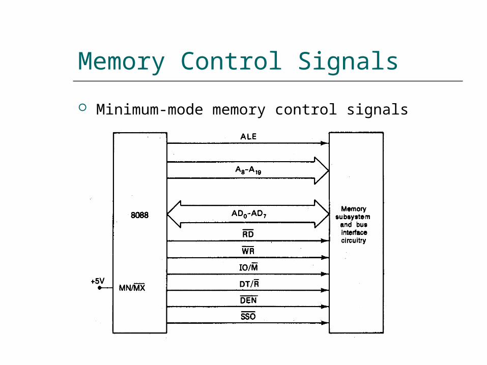
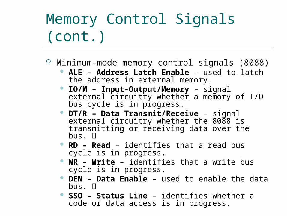
Read and Write Bus Cycle (cont)
Read cycle
Minimum-mode memory read bus cycle of the 8086
Read and Write Bus Cycle (cont)
Read cycle
Maximum-mode memory read bus cycle of the 8086
Read and Write Bus Cycle (cont)
Write cycle
Minimum-mode memory write bus cycle of the 8088
Read and Write Bus Cycle (cont)
Write cycle
Maximum-mode memory write bus cycle of the 8086
Memory Interface Circuit
Address bus latches and buffers Bank write and bank read control logic Data bus transceiversbuffers Address decoders
Memory Interface Circuit (cont)
Memory interface block diagram
Memory Interface Circuit (cont)
Address bus latches and buffers
Block diagram of a D-type latch
Memory Interface Circuit (cont)
Address bus latches and buffers
Circuit diagram of the 74F373
Memory Interface Circuit (cont)
A review of flip-floplatch logic
Positive edge-triggered D flip-flop
Memory Interface Circuit (cont)
A review of flip-floplatch logic
Positive edge-triggered JK flip-flop
Memory Interface Circuit (cont)
A review of flip-floplatch logic
D-type latch
Memory Interface Circuit (cont)
Address bus latches and buffers
Address latch circuit
Memory Interface Circuit (cont)
Bank write and bank read control logic
Bank write control logic Bank read control logic
Memory Interface Circuit (cont)
Data bus transceivers
Block diagram and circuit diagram of the 74F245 octal bus transceiver
Memory Interface Circuit (cont)
Data bus transceivers
Data bus transceiver circuit
Memory Interface Circuit (cont)
Address decoder
Address bus configuration with address decoding
Memory Interface Circuit (cont)
Address decoder
Block diagram and operation of the 74F139 decoder
Memory Interface Circuit (cont)
Address decoder
Circuit diagram of the 74F139 decoder
Memory Interface Circuit (cont)
Address decoder
Address decoder circuit using 74F139
Memory Interface Circuit (cont)
Address decoder
Block diagram and operation of the 74F138 decoder
Memory Interface Circuit (cont)
Address decoder
Circuit diagram of the 74F138 decoder
Memory Interface Circuit (cont)
Address decoder
Address decoder circuit using 74F138
Types of InputOutput
The IO system allows peripherals to provide data or receive results of processing the data Using IO ports
The 80888086 MPU can employ two types of IO Isolated IO Memory-mapped IO
They differ in how IO ports are mapped into the address space
Types of InputOutput (cont)
Isolated inputoutput When using isolated IO in a microcomputer
system the IO device are treated separate from memory
The memory address space contains 1 M consecutive byte address in the range 0000016 through FFFFF16
The IO address space contains 64K consecutive byte addresses in the range 000016 through FFFF16
The bytes in two consecutive IO addresses can be accessed as word-wide data
Page 0 000016 00FF16
Certain IO instructions can only perform in this range
Types of InputOutput (cont)
Isolated inputoutput
80888086 memory and IO address spaces
Types of InputOutput (cont)
Isolated inputoutput
Isolated IO ports
Types of InputOutput (cont)
Isolated inputoutput Advantages
The complete 1Mbyte memory address space is available for use with memory
Special instructions have been provided to perform IO operations with maximized performance
The bytes in two consecutive IO addresses can be accessed as word-wide data
Disadvantages All input and output data transfers must take place
between the AL or AX register and IO port
Types of InputOutput (cont)
Memory-mapped inputoutput MPU looks at the IO port as though it is a storage
location in memory Some of the memory address space is dedicated to IO
ports Instructions that affect data in memory are used
instead of the special IO instructions More instructions and addressing modes are available to
perform IO operations IO transfers can take place between IO port and other
internal registers The memory instructions tend to execute slower
than those specifically designed for isolated IO Part of the memory address space is lost
Types of InputOutput(cont)
Memory-mapped inputoutput
Memory mapped IO ports
Isolated InputOutput Interface
IO devices Keyboard Printer Mouse 82C55A etc
Functions of interface circuit Select the IO port Latch output data Sample input data Synchronize data transfer Translate between TTL voltage levels and those
required to operate the IO devices
Isolated InputOutput Interface (cont)
Minimum-mode interface
Minimum-mode 8088 system IO interface
Isolated InputOutput Interface (cont)
Minimum-mode interface
Minimum-mode 8086 system IO interface
Isolated InputOutput Interface (cont)
Maximum-mode interface
Maximum-mode 8088 system IO interface
Isolated InputOutput Interface (cont)
Maximum-mode interface
Maximum-mode 8086 system IO interface
Isolated InputOutput Interface (cont)
Maximum-mode interface
IO bus cycle status codes
InputOutput Data Transfer
Inputoutput data transfers in the 8088 and 8086 microcomputers can be either byte-wide or word-wide
IO addresses are 16 bits in length and are output by the 8088 to the IO interface over bus lines AD0 through AD7 and A8 through A15
In 8088 the word transfers is performed as two consecutive byte-wide data transfer and takes two bus cycle
In 8086 the word transfers can takes either one or two bus cycle
Word-wide IO ports should be aligned at even-address boundaries
InputOutput Data Instructions
InputOutput Data Instructions(cont)
EXAMPLE Write a sequence of instructions that will output
the data FF16 to a byte-wide output port at address AB16 of the IO address space
Solution First the AL register is loaded with FF16 as an
immediate operand in the instruction
MOV AL 0FFH Now the data in AL can be output to the byte-
wide output port with the instruction
OUT 0ABH AL
InputOutput Data Instructions(cont)
EXAMPLE Write a series of instructions that will output FF16 to an
output port located at address B00016 of the IO address space
Solution The DX register must first be loaded with the address
of the output port This is done with the instructionMOV DX 0B000H
Next the data that are to be output must be loaded into AL with the instruction
MOV AL 0FFH Finally the data are output with the instruction
OUT DX AL
InputOutput Data Instructions(cont)
EXAMPLE Data are to be read in from two byte-wide input
ports at addresses AA16 and A916 and then output as a word-wide output port at address B00016 Write a sequence of instructions to perform this inputoutput operation
InputOutput Data Instructions(cont)
Solution First read in the byte at address AA16 into AL and
move it into AHIN AL 0AAHMOV AH AL
Now the other byte can be read into AL by the instructionIN AL 09AH
And to write out the word of dataMOV DX 0B000HOUT DX AX
InputOutput Bus Cycles
Input bus cycle of the 8088
InputOutput Bus Cycles (cont)
Output bus cycle of the 8088
InputOutput Bus Cycles (cont)
Input bus cycle of the 8086
InputOutput Bus Cycles (cont)
Output bus cycle of the 8086
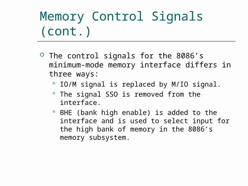
Read and Write Bus Cycle (cont)
Read cycle
Maximum-mode memory read bus cycle of the 8086
Read and Write Bus Cycle (cont)
Write cycle
Minimum-mode memory write bus cycle of the 8088
Read and Write Bus Cycle (cont)
Write cycle
Maximum-mode memory write bus cycle of the 8086
Memory Interface Circuit
Address bus latches and buffers Bank write and bank read control logic Data bus transceiversbuffers Address decoders
Memory Interface Circuit (cont)
Memory interface block diagram
Memory Interface Circuit (cont)
Address bus latches and buffers
Block diagram of a D-type latch
Memory Interface Circuit (cont)
Address bus latches and buffers
Circuit diagram of the 74F373
Memory Interface Circuit (cont)
A review of flip-floplatch logic
Positive edge-triggered D flip-flop
Memory Interface Circuit (cont)
A review of flip-floplatch logic
Positive edge-triggered JK flip-flop
Memory Interface Circuit (cont)
A review of flip-floplatch logic
D-type latch
Memory Interface Circuit (cont)
Address bus latches and buffers
Address latch circuit
Memory Interface Circuit (cont)
Bank write and bank read control logic
Bank write control logic Bank read control logic
Memory Interface Circuit (cont)
Data bus transceivers
Block diagram and circuit diagram of the 74F245 octal bus transceiver
Memory Interface Circuit (cont)
Data bus transceivers
Data bus transceiver circuit
Memory Interface Circuit (cont)
Address decoder
Address bus configuration with address decoding
Memory Interface Circuit (cont)
Address decoder
Block diagram and operation of the 74F139 decoder
Memory Interface Circuit (cont)
Address decoder
Circuit diagram of the 74F139 decoder
Memory Interface Circuit (cont)
Address decoder
Address decoder circuit using 74F139
Memory Interface Circuit (cont)
Address decoder
Block diagram and operation of the 74F138 decoder
Memory Interface Circuit (cont)
Address decoder
Circuit diagram of the 74F138 decoder
Memory Interface Circuit (cont)
Address decoder
Address decoder circuit using 74F138
Types of InputOutput
The IO system allows peripherals to provide data or receive results of processing the data Using IO ports
The 80888086 MPU can employ two types of IO Isolated IO Memory-mapped IO
They differ in how IO ports are mapped into the address space
Types of InputOutput (cont)
Isolated inputoutput When using isolated IO in a microcomputer
system the IO device are treated separate from memory
The memory address space contains 1 M consecutive byte address in the range 0000016 through FFFFF16
The IO address space contains 64K consecutive byte addresses in the range 000016 through FFFF16
The bytes in two consecutive IO addresses can be accessed as word-wide data
Page 0 000016 00FF16
Certain IO instructions can only perform in this range
Types of InputOutput (cont)
Isolated inputoutput
80888086 memory and IO address spaces
Types of InputOutput (cont)
Isolated inputoutput
Isolated IO ports
Types of InputOutput (cont)
Isolated inputoutput Advantages
The complete 1Mbyte memory address space is available for use with memory
Special instructions have been provided to perform IO operations with maximized performance
The bytes in two consecutive IO addresses can be accessed as word-wide data
Disadvantages All input and output data transfers must take place
between the AL or AX register and IO port
Types of InputOutput (cont)
Memory-mapped inputoutput MPU looks at the IO port as though it is a storage
location in memory Some of the memory address space is dedicated to IO
ports Instructions that affect data in memory are used
instead of the special IO instructions More instructions and addressing modes are available to
perform IO operations IO transfers can take place between IO port and other
internal registers The memory instructions tend to execute slower
than those specifically designed for isolated IO Part of the memory address space is lost
Types of InputOutput(cont)
Memory-mapped inputoutput
Memory mapped IO ports
Isolated InputOutput Interface
IO devices Keyboard Printer Mouse 82C55A etc
Functions of interface circuit Select the IO port Latch output data Sample input data Synchronize data transfer Translate between TTL voltage levels and those
required to operate the IO devices
Isolated InputOutput Interface (cont)
Minimum-mode interface
Minimum-mode 8088 system IO interface
Isolated InputOutput Interface (cont)
Minimum-mode interface
Minimum-mode 8086 system IO interface
Isolated InputOutput Interface (cont)
Maximum-mode interface
Maximum-mode 8088 system IO interface
Isolated InputOutput Interface (cont)
Maximum-mode interface
Maximum-mode 8086 system IO interface
Isolated InputOutput Interface (cont)
Maximum-mode interface
IO bus cycle status codes
InputOutput Data Transfer
Inputoutput data transfers in the 8088 and 8086 microcomputers can be either byte-wide or word-wide
IO addresses are 16 bits in length and are output by the 8088 to the IO interface over bus lines AD0 through AD7 and A8 through A15
In 8088 the word transfers is performed as two consecutive byte-wide data transfer and takes two bus cycle
In 8086 the word transfers can takes either one or two bus cycle
Word-wide IO ports should be aligned at even-address boundaries
InputOutput Data Instructions
InputOutput Data Instructions(cont)
EXAMPLE Write a sequence of instructions that will output
the data FF16 to a byte-wide output port at address AB16 of the IO address space
Solution First the AL register is loaded with FF16 as an
immediate operand in the instruction
MOV AL 0FFH Now the data in AL can be output to the byte-
wide output port with the instruction
OUT 0ABH AL
InputOutput Data Instructions(cont)
EXAMPLE Write a series of instructions that will output FF16 to an
output port located at address B00016 of the IO address space
Solution The DX register must first be loaded with the address
of the output port This is done with the instructionMOV DX 0B000H
Next the data that are to be output must be loaded into AL with the instruction
MOV AL 0FFH Finally the data are output with the instruction
OUT DX AL
InputOutput Data Instructions(cont)
EXAMPLE Data are to be read in from two byte-wide input
ports at addresses AA16 and A916 and then output as a word-wide output port at address B00016 Write a sequence of instructions to perform this inputoutput operation
InputOutput Data Instructions(cont)
Solution First read in the byte at address AA16 into AL and
move it into AHIN AL 0AAHMOV AH AL
Now the other byte can be read into AL by the instructionIN AL 09AH
And to write out the word of dataMOV DX 0B000HOUT DX AX
InputOutput Bus Cycles
Input bus cycle of the 8088
InputOutput Bus Cycles (cont)
Output bus cycle of the 8088
InputOutput Bus Cycles (cont)
Input bus cycle of the 8086
InputOutput Bus Cycles (cont)
Output bus cycle of the 8086
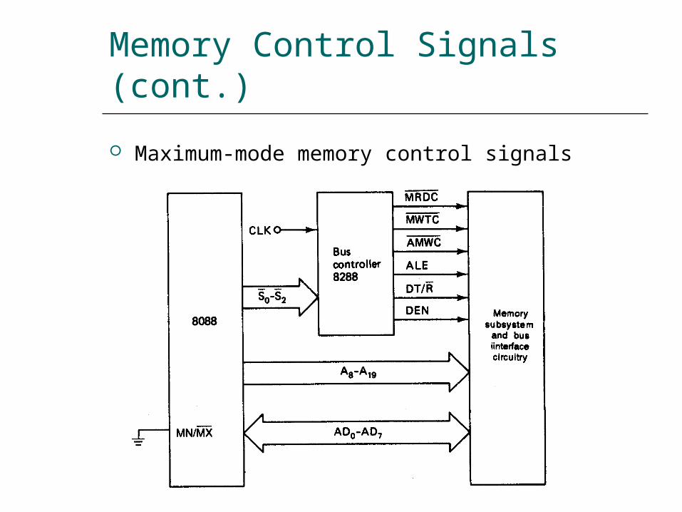
Read and Write Bus Cycle (cont)
Write cycle
Minimum-mode memory write bus cycle of the 8088
Read and Write Bus Cycle (cont)
Write cycle
Maximum-mode memory write bus cycle of the 8086
Memory Interface Circuit
Address bus latches and buffers Bank write and bank read control logic Data bus transceiversbuffers Address decoders
Memory Interface Circuit (cont)
Memory interface block diagram
Memory Interface Circuit (cont)
Address bus latches and buffers
Block diagram of a D-type latch
Memory Interface Circuit (cont)
Address bus latches and buffers
Circuit diagram of the 74F373
Memory Interface Circuit (cont)
A review of flip-floplatch logic
Positive edge-triggered D flip-flop
Memory Interface Circuit (cont)
A review of flip-floplatch logic
Positive edge-triggered JK flip-flop
Memory Interface Circuit (cont)
A review of flip-floplatch logic
D-type latch
Memory Interface Circuit (cont)
Address bus latches and buffers
Address latch circuit
Memory Interface Circuit (cont)
Bank write and bank read control logic
Bank write control logic Bank read control logic
Memory Interface Circuit (cont)
Data bus transceivers
Block diagram and circuit diagram of the 74F245 octal bus transceiver
Memory Interface Circuit (cont)
Data bus transceivers
Data bus transceiver circuit
Memory Interface Circuit (cont)
Address decoder
Address bus configuration with address decoding
Memory Interface Circuit (cont)
Address decoder
Block diagram and operation of the 74F139 decoder
Memory Interface Circuit (cont)
Address decoder
Circuit diagram of the 74F139 decoder
Memory Interface Circuit (cont)
Address decoder
Address decoder circuit using 74F139
Memory Interface Circuit (cont)
Address decoder
Block diagram and operation of the 74F138 decoder
Memory Interface Circuit (cont)
Address decoder
Circuit diagram of the 74F138 decoder
Memory Interface Circuit (cont)
Address decoder
Address decoder circuit using 74F138
Types of InputOutput
The IO system allows peripherals to provide data or receive results of processing the data Using IO ports
The 80888086 MPU can employ two types of IO Isolated IO Memory-mapped IO
They differ in how IO ports are mapped into the address space
Types of InputOutput (cont)
Isolated inputoutput When using isolated IO in a microcomputer
system the IO device are treated separate from memory
The memory address space contains 1 M consecutive byte address in the range 0000016 through FFFFF16
The IO address space contains 64K consecutive byte addresses in the range 000016 through FFFF16
The bytes in two consecutive IO addresses can be accessed as word-wide data
Page 0 000016 00FF16
Certain IO instructions can only perform in this range
Types of InputOutput (cont)
Isolated inputoutput
80888086 memory and IO address spaces
Types of InputOutput (cont)
Isolated inputoutput
Isolated IO ports
Types of InputOutput (cont)
Isolated inputoutput Advantages
The complete 1Mbyte memory address space is available for use with memory
Special instructions have been provided to perform IO operations with maximized performance
The bytes in two consecutive IO addresses can be accessed as word-wide data
Disadvantages All input and output data transfers must take place
between the AL or AX register and IO port
Types of InputOutput (cont)
Memory-mapped inputoutput MPU looks at the IO port as though it is a storage
location in memory Some of the memory address space is dedicated to IO
ports Instructions that affect data in memory are used
instead of the special IO instructions More instructions and addressing modes are available to
perform IO operations IO transfers can take place between IO port and other
internal registers The memory instructions tend to execute slower
than those specifically designed for isolated IO Part of the memory address space is lost
Types of InputOutput(cont)
Memory-mapped inputoutput
Memory mapped IO ports
Isolated InputOutput Interface
IO devices Keyboard Printer Mouse 82C55A etc
Functions of interface circuit Select the IO port Latch output data Sample input data Synchronize data transfer Translate between TTL voltage levels and those
required to operate the IO devices
Isolated InputOutput Interface (cont)
Minimum-mode interface
Minimum-mode 8088 system IO interface
Isolated InputOutput Interface (cont)
Minimum-mode interface
Minimum-mode 8086 system IO interface
Isolated InputOutput Interface (cont)
Maximum-mode interface
Maximum-mode 8088 system IO interface
Isolated InputOutput Interface (cont)
Maximum-mode interface
Maximum-mode 8086 system IO interface
Isolated InputOutput Interface (cont)
Maximum-mode interface
IO bus cycle status codes
InputOutput Data Transfer
Inputoutput data transfers in the 8088 and 8086 microcomputers can be either byte-wide or word-wide
IO addresses are 16 bits in length and are output by the 8088 to the IO interface over bus lines AD0 through AD7 and A8 through A15
In 8088 the word transfers is performed as two consecutive byte-wide data transfer and takes two bus cycle
In 8086 the word transfers can takes either one or two bus cycle
Word-wide IO ports should be aligned at even-address boundaries
InputOutput Data Instructions
InputOutput Data Instructions(cont)
EXAMPLE Write a sequence of instructions that will output
the data FF16 to a byte-wide output port at address AB16 of the IO address space
Solution First the AL register is loaded with FF16 as an
immediate operand in the instruction
MOV AL 0FFH Now the data in AL can be output to the byte-
wide output port with the instruction
OUT 0ABH AL
InputOutput Data Instructions(cont)
EXAMPLE Write a series of instructions that will output FF16 to an
output port located at address B00016 of the IO address space
Solution The DX register must first be loaded with the address
of the output port This is done with the instructionMOV DX 0B000H
Next the data that are to be output must be loaded into AL with the instruction
MOV AL 0FFH Finally the data are output with the instruction
OUT DX AL
InputOutput Data Instructions(cont)
EXAMPLE Data are to be read in from two byte-wide input
ports at addresses AA16 and A916 and then output as a word-wide output port at address B00016 Write a sequence of instructions to perform this inputoutput operation
InputOutput Data Instructions(cont)
Solution First read in the byte at address AA16 into AL and
move it into AHIN AL 0AAHMOV AH AL
Now the other byte can be read into AL by the instructionIN AL 09AH
And to write out the word of dataMOV DX 0B000HOUT DX AX
InputOutput Bus Cycles
Input bus cycle of the 8088
InputOutput Bus Cycles (cont)
Output bus cycle of the 8088
InputOutput Bus Cycles (cont)
Input bus cycle of the 8086
InputOutput Bus Cycles (cont)
Output bus cycle of the 8086
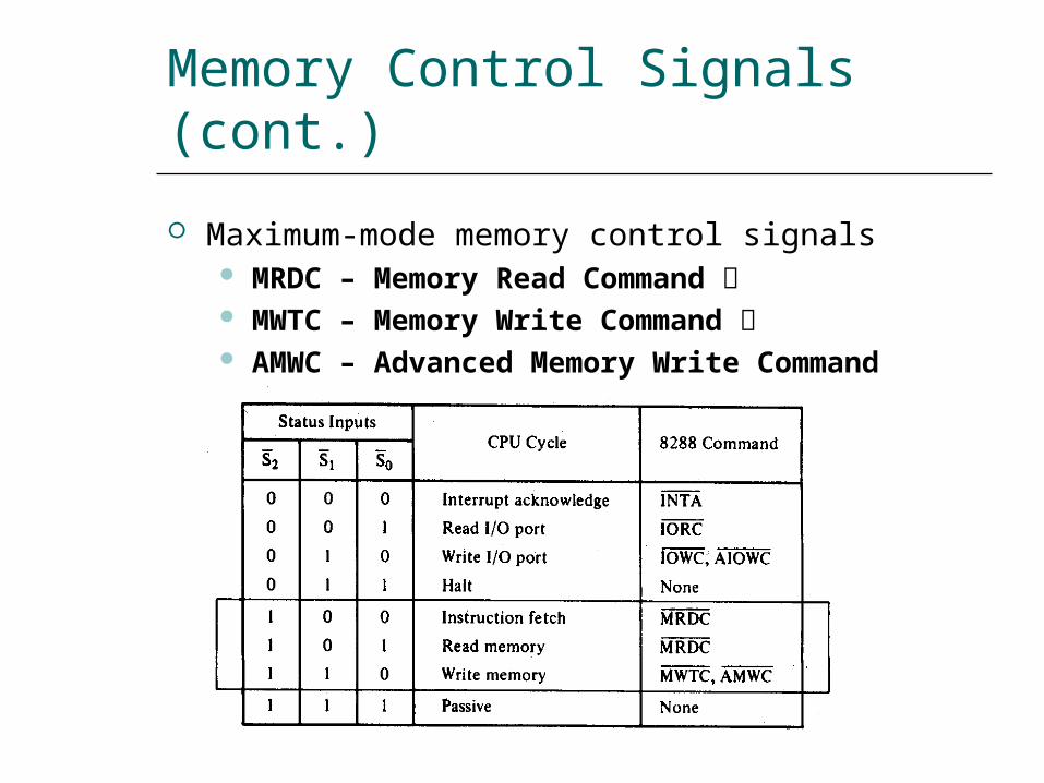
Read and Write Bus Cycle (cont)
Write cycle
Maximum-mode memory write bus cycle of the 8086
Memory Interface Circuit
Address bus latches and buffers Bank write and bank read control logic Data bus transceiversbuffers Address decoders
Memory Interface Circuit (cont)
Memory interface block diagram
Memory Interface Circuit (cont)
Address bus latches and buffers
Block diagram of a D-type latch
Memory Interface Circuit (cont)
Address bus latches and buffers
Circuit diagram of the 74F373
Memory Interface Circuit (cont)
A review of flip-floplatch logic
Positive edge-triggered D flip-flop
Memory Interface Circuit (cont)
A review of flip-floplatch logic
Positive edge-triggered JK flip-flop
Memory Interface Circuit (cont)
A review of flip-floplatch logic
D-type latch
Memory Interface Circuit (cont)
Address bus latches and buffers
Address latch circuit
Memory Interface Circuit (cont)
Bank write and bank read control logic
Bank write control logic Bank read control logic
Memory Interface Circuit (cont)
Data bus transceivers
Block diagram and circuit diagram of the 74F245 octal bus transceiver
Memory Interface Circuit (cont)
Data bus transceivers
Data bus transceiver circuit
Memory Interface Circuit (cont)
Address decoder
Address bus configuration with address decoding
Memory Interface Circuit (cont)
Address decoder
Block diagram and operation of the 74F139 decoder
Memory Interface Circuit (cont)
Address decoder
Circuit diagram of the 74F139 decoder
Memory Interface Circuit (cont)
Address decoder
Address decoder circuit using 74F139
Memory Interface Circuit (cont)
Address decoder
Block diagram and operation of the 74F138 decoder
Memory Interface Circuit (cont)
Address decoder
Circuit diagram of the 74F138 decoder
Memory Interface Circuit (cont)
Address decoder
Address decoder circuit using 74F138
Types of InputOutput
The IO system allows peripherals to provide data or receive results of processing the data Using IO ports
The 80888086 MPU can employ two types of IO Isolated IO Memory-mapped IO
They differ in how IO ports are mapped into the address space
Types of InputOutput (cont)
Isolated inputoutput When using isolated IO in a microcomputer
system the IO device are treated separate from memory
The memory address space contains 1 M consecutive byte address in the range 0000016 through FFFFF16
The IO address space contains 64K consecutive byte addresses in the range 000016 through FFFF16
The bytes in two consecutive IO addresses can be accessed as word-wide data
Page 0 000016 00FF16
Certain IO instructions can only perform in this range
Types of InputOutput (cont)
Isolated inputoutput
80888086 memory and IO address spaces
Types of InputOutput (cont)
Isolated inputoutput
Isolated IO ports
Types of InputOutput (cont)
Isolated inputoutput Advantages
The complete 1Mbyte memory address space is available for use with memory
Special instructions have been provided to perform IO operations with maximized performance
The bytes in two consecutive IO addresses can be accessed as word-wide data
Disadvantages All input and output data transfers must take place
between the AL or AX register and IO port
Types of InputOutput (cont)
Memory-mapped inputoutput MPU looks at the IO port as though it is a storage
location in memory Some of the memory address space is dedicated to IO
ports Instructions that affect data in memory are used
instead of the special IO instructions More instructions and addressing modes are available to
perform IO operations IO transfers can take place between IO port and other
internal registers The memory instructions tend to execute slower
than those specifically designed for isolated IO Part of the memory address space is lost
Types of InputOutput(cont)
Memory-mapped inputoutput
Memory mapped IO ports
Isolated InputOutput Interface
IO devices Keyboard Printer Mouse 82C55A etc
Functions of interface circuit Select the IO port Latch output data Sample input data Synchronize data transfer Translate between TTL voltage levels and those
required to operate the IO devices
Isolated InputOutput Interface (cont)
Minimum-mode interface
Minimum-mode 8088 system IO interface
Isolated InputOutput Interface (cont)
Minimum-mode interface
Minimum-mode 8086 system IO interface
Isolated InputOutput Interface (cont)
Maximum-mode interface
Maximum-mode 8088 system IO interface
Isolated InputOutput Interface (cont)
Maximum-mode interface
Maximum-mode 8086 system IO interface
Isolated InputOutput Interface (cont)
Maximum-mode interface
IO bus cycle status codes
InputOutput Data Transfer
Inputoutput data transfers in the 8088 and 8086 microcomputers can be either byte-wide or word-wide
IO addresses are 16 bits in length and are output by the 8088 to the IO interface over bus lines AD0 through AD7 and A8 through A15
In 8088 the word transfers is performed as two consecutive byte-wide data transfer and takes two bus cycle
In 8086 the word transfers can takes either one or two bus cycle
Word-wide IO ports should be aligned at even-address boundaries
InputOutput Data Instructions
InputOutput Data Instructions(cont)
EXAMPLE Write a sequence of instructions that will output
the data FF16 to a byte-wide output port at address AB16 of the IO address space
Solution First the AL register is loaded with FF16 as an
immediate operand in the instruction
MOV AL 0FFH Now the data in AL can be output to the byte-
wide output port with the instruction
OUT 0ABH AL
InputOutput Data Instructions(cont)
EXAMPLE Write a series of instructions that will output FF16 to an
output port located at address B00016 of the IO address space
Solution The DX register must first be loaded with the address
of the output port This is done with the instructionMOV DX 0B000H
Next the data that are to be output must be loaded into AL with the instruction
MOV AL 0FFH Finally the data are output with the instruction
OUT DX AL
InputOutput Data Instructions(cont)
EXAMPLE Data are to be read in from two byte-wide input
ports at addresses AA16 and A916 and then output as a word-wide output port at address B00016 Write a sequence of instructions to perform this inputoutput operation
InputOutput Data Instructions(cont)
Solution First read in the byte at address AA16 into AL and
move it into AHIN AL 0AAHMOV AH AL
Now the other byte can be read into AL by the instructionIN AL 09AH
And to write out the word of dataMOV DX 0B000HOUT DX AX
InputOutput Bus Cycles
Input bus cycle of the 8088
InputOutput Bus Cycles (cont)
Output bus cycle of the 8088
InputOutput Bus Cycles (cont)
Input bus cycle of the 8086
InputOutput Bus Cycles (cont)
Output bus cycle of the 8086
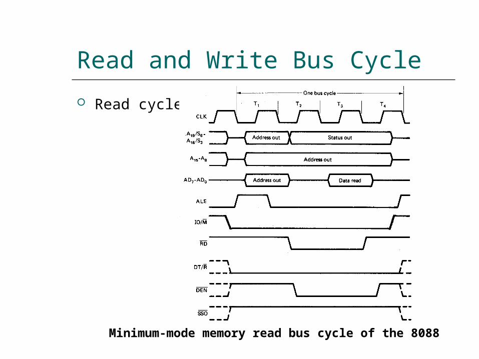
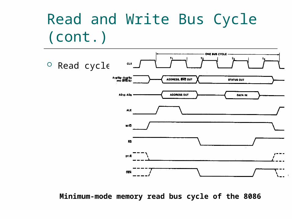
Memory Interface Circuit (cont)
Memory interface block diagram
Memory Interface Circuit (cont)
Address bus latches and buffers
Block diagram of a D-type latch
Memory Interface Circuit (cont)
Address bus latches and buffers
Circuit diagram of the 74F373
Memory Interface Circuit (cont)
A review of flip-floplatch logic
Positive edge-triggered D flip-flop
Memory Interface Circuit (cont)
A review of flip-floplatch logic
Positive edge-triggered JK flip-flop
Memory Interface Circuit (cont)
A review of flip-floplatch logic
D-type latch
Memory Interface Circuit (cont)
Address bus latches and buffers
Address latch circuit
Memory Interface Circuit (cont)
Bank write and bank read control logic
Bank write control logic Bank read control logic
Memory Interface Circuit (cont)
Data bus transceivers
Block diagram and circuit diagram of the 74F245 octal bus transceiver
Memory Interface Circuit (cont)
Data bus transceivers
Data bus transceiver circuit
Memory Interface Circuit (cont)
Address decoder
Address bus configuration with address decoding
Memory Interface Circuit (cont)
Address decoder
Block diagram and operation of the 74F139 decoder
Memory Interface Circuit (cont)
Address decoder
Circuit diagram of the 74F139 decoder
Memory Interface Circuit (cont)
Address decoder
Address decoder circuit using 74F139
Memory Interface Circuit (cont)
Address decoder
Block diagram and operation of the 74F138 decoder
Memory Interface Circuit (cont)
Address decoder
Circuit diagram of the 74F138 decoder
Memory Interface Circuit (cont)
Address decoder
Address decoder circuit using 74F138
Types of InputOutput
The IO system allows peripherals to provide data or receive results of processing the data Using IO ports
The 80888086 MPU can employ two types of IO Isolated IO Memory-mapped IO
They differ in how IO ports are mapped into the address space
Types of InputOutput (cont)
Isolated inputoutput When using isolated IO in a microcomputer
system the IO device are treated separate from memory
The memory address space contains 1 M consecutive byte address in the range 0000016 through FFFFF16
The IO address space contains 64K consecutive byte addresses in the range 000016 through FFFF16
The bytes in two consecutive IO addresses can be accessed as word-wide data
Page 0 000016 00FF16
Certain IO instructions can only perform in this range
Types of InputOutput (cont)
Isolated inputoutput
80888086 memory and IO address spaces
Types of InputOutput (cont)
Isolated inputoutput
Isolated IO ports
Types of InputOutput (cont)
Isolated inputoutput Advantages
The complete 1Mbyte memory address space is available for use with memory
Special instructions have been provided to perform IO operations with maximized performance
The bytes in two consecutive IO addresses can be accessed as word-wide data
Disadvantages All input and output data transfers must take place
between the AL or AX register and IO port
Types of InputOutput (cont)
Memory-mapped inputoutput MPU looks at the IO port as though it is a storage
location in memory Some of the memory address space is dedicated to IO
ports Instructions that affect data in memory are used
instead of the special IO instructions More instructions and addressing modes are available to
perform IO operations IO transfers can take place between IO port and other
internal registers The memory instructions tend to execute slower
than those specifically designed for isolated IO Part of the memory address space is lost
Types of InputOutput(cont)
Memory-mapped inputoutput
Memory mapped IO ports
Isolated InputOutput Interface
IO devices Keyboard Printer Mouse 82C55A etc
Functions of interface circuit Select the IO port Latch output data Sample input data Synchronize data transfer Translate between TTL voltage levels and those
required to operate the IO devices
Isolated InputOutput Interface (cont)
Minimum-mode interface
Minimum-mode 8088 system IO interface
Isolated InputOutput Interface (cont)
Minimum-mode interface
Minimum-mode 8086 system IO interface
Isolated InputOutput Interface (cont)
Maximum-mode interface
Maximum-mode 8088 system IO interface
Isolated InputOutput Interface (cont)
Maximum-mode interface
Maximum-mode 8086 system IO interface
Isolated InputOutput Interface (cont)
Maximum-mode interface
IO bus cycle status codes
InputOutput Data Transfer
Inputoutput data transfers in the 8088 and 8086 microcomputers can be either byte-wide or word-wide
IO addresses are 16 bits in length and are output by the 8088 to the IO interface over bus lines AD0 through AD7 and A8 through A15
In 8088 the word transfers is performed as two consecutive byte-wide data transfer and takes two bus cycle
In 8086 the word transfers can takes either one or two bus cycle
Word-wide IO ports should be aligned at even-address boundaries
InputOutput Data Instructions
InputOutput Data Instructions(cont)
EXAMPLE Write a sequence of instructions that will output
the data FF16 to a byte-wide output port at address AB16 of the IO address space
Solution First the AL register is loaded with FF16 as an
immediate operand in the instruction
MOV AL 0FFH Now the data in AL can be output to the byte-
wide output port with the instruction
OUT 0ABH AL
InputOutput Data Instructions(cont)
EXAMPLE Write a series of instructions that will output FF16 to an
output port located at address B00016 of the IO address space
Solution The DX register must first be loaded with the address
of the output port This is done with the instructionMOV DX 0B000H
Next the data that are to be output must be loaded into AL with the instruction
MOV AL 0FFH Finally the data are output with the instruction
OUT DX AL
InputOutput Data Instructions(cont)
EXAMPLE Data are to be read in from two byte-wide input
ports at addresses AA16 and A916 and then output as a word-wide output port at address B00016 Write a sequence of instructions to perform this inputoutput operation
InputOutput Data Instructions(cont)
Solution First read in the byte at address AA16 into AL and
move it into AHIN AL 0AAHMOV AH AL
Now the other byte can be read into AL by the instructionIN AL 09AH
And to write out the word of dataMOV DX 0B000HOUT DX AX
InputOutput Bus Cycles
Input bus cycle of the 8088
InputOutput Bus Cycles (cont)
Output bus cycle of the 8088
InputOutput Bus Cycles (cont)
Input bus cycle of the 8086
InputOutput Bus Cycles (cont)
Output bus cycle of the 8086
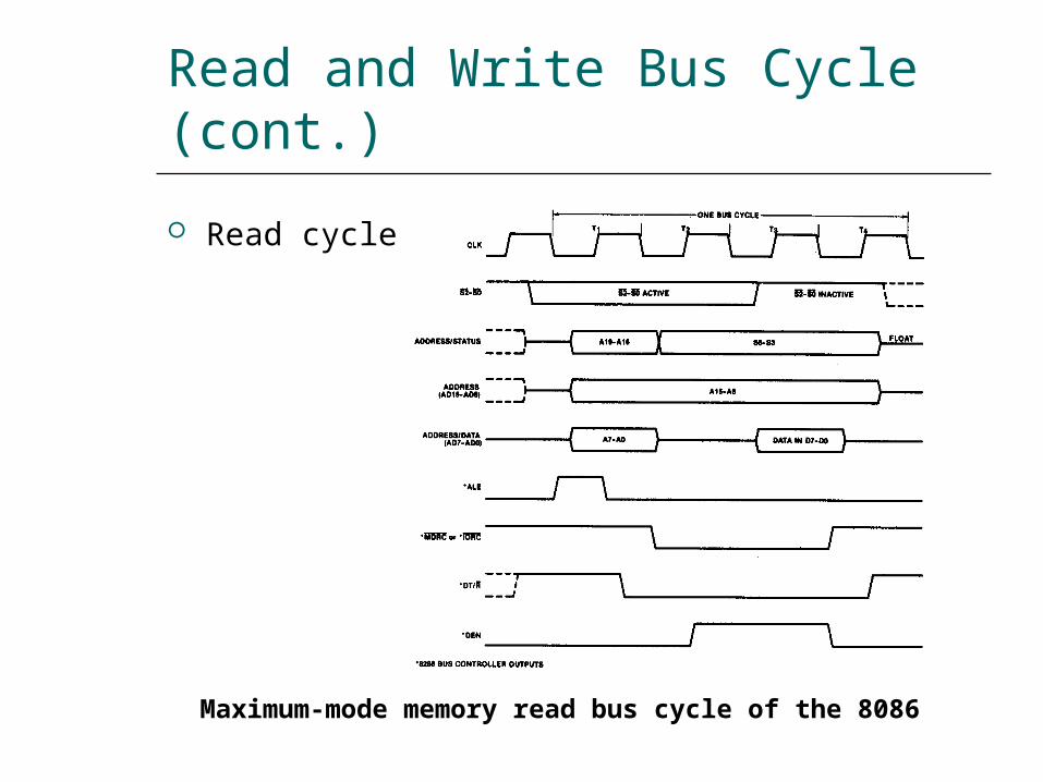
Memory Interface Circuit (cont)
Address bus latches and buffers
Block diagram of a D-type latch
Memory Interface Circuit (cont)
Address bus latches and buffers
Circuit diagram of the 74F373
Memory Interface Circuit (cont)
A review of flip-floplatch logic
Positive edge-triggered D flip-flop
Memory Interface Circuit (cont)
A review of flip-floplatch logic
Positive edge-triggered JK flip-flop
Memory Interface Circuit (cont)
A review of flip-floplatch logic
D-type latch
Memory Interface Circuit (cont)
Address bus latches and buffers
Address latch circuit
Memory Interface Circuit (cont)
Bank write and bank read control logic
Bank write control logic Bank read control logic
Memory Interface Circuit (cont)
Data bus transceivers
Block diagram and circuit diagram of the 74F245 octal bus transceiver
Memory Interface Circuit (cont)
Data bus transceivers
Data bus transceiver circuit
Memory Interface Circuit (cont)
Address decoder
Address bus configuration with address decoding
Memory Interface Circuit (cont)
Address decoder
Block diagram and operation of the 74F139 decoder
Memory Interface Circuit (cont)
Address decoder
Circuit diagram of the 74F139 decoder
Memory Interface Circuit (cont)
Address decoder
Address decoder circuit using 74F139
Memory Interface Circuit (cont)
Address decoder
Block diagram and operation of the 74F138 decoder
Memory Interface Circuit (cont)
Address decoder
Circuit diagram of the 74F138 decoder
Memory Interface Circuit (cont)
Address decoder
Address decoder circuit using 74F138
Types of InputOutput
The IO system allows peripherals to provide data or receive results of processing the data Using IO ports
The 80888086 MPU can employ two types of IO Isolated IO Memory-mapped IO
They differ in how IO ports are mapped into the address space
Types of InputOutput (cont)
Isolated inputoutput When using isolated IO in a microcomputer
system the IO device are treated separate from memory
The memory address space contains 1 M consecutive byte address in the range 0000016 through FFFFF16
The IO address space contains 64K consecutive byte addresses in the range 000016 through FFFF16
The bytes in two consecutive IO addresses can be accessed as word-wide data
Page 0 000016 00FF16
Certain IO instructions can only perform in this range
Types of InputOutput (cont)
Isolated inputoutput
80888086 memory and IO address spaces
Types of InputOutput (cont)
Isolated inputoutput
Isolated IO ports
Types of InputOutput (cont)
Isolated inputoutput Advantages
The complete 1Mbyte memory address space is available for use with memory
Special instructions have been provided to perform IO operations with maximized performance
The bytes in two consecutive IO addresses can be accessed as word-wide data
Disadvantages All input and output data transfers must take place
between the AL or AX register and IO port
Types of InputOutput (cont)
Memory-mapped inputoutput MPU looks at the IO port as though it is a storage
location in memory Some of the memory address space is dedicated to IO
ports Instructions that affect data in memory are used
instead of the special IO instructions More instructions and addressing modes are available to
perform IO operations IO transfers can take place between IO port and other
internal registers The memory instructions tend to execute slower
than those specifically designed for isolated IO Part of the memory address space is lost
Types of InputOutput(cont)
Memory-mapped inputoutput
Memory mapped IO ports
Isolated InputOutput Interface
IO devices Keyboard Printer Mouse 82C55A etc
Functions of interface circuit Select the IO port Latch output data Sample input data Synchronize data transfer Translate between TTL voltage levels and those
required to operate the IO devices
Isolated InputOutput Interface (cont)
Minimum-mode interface
Minimum-mode 8088 system IO interface
Isolated InputOutput Interface (cont)
Minimum-mode interface
Minimum-mode 8086 system IO interface
Isolated InputOutput Interface (cont)
Maximum-mode interface
Maximum-mode 8088 system IO interface
Isolated InputOutput Interface (cont)
Maximum-mode interface
Maximum-mode 8086 system IO interface
Isolated InputOutput Interface (cont)
Maximum-mode interface
IO bus cycle status codes
InputOutput Data Transfer
Inputoutput data transfers in the 8088 and 8086 microcomputers can be either byte-wide or word-wide
IO addresses are 16 bits in length and are output by the 8088 to the IO interface over bus lines AD0 through AD7 and A8 through A15
In 8088 the word transfers is performed as two consecutive byte-wide data transfer and takes two bus cycle
In 8086 the word transfers can takes either one or two bus cycle
Word-wide IO ports should be aligned at even-address boundaries
InputOutput Data Instructions
InputOutput Data Instructions(cont)
EXAMPLE Write a sequence of instructions that will output
the data FF16 to a byte-wide output port at address AB16 of the IO address space
Solution First the AL register is loaded with FF16 as an
immediate operand in the instruction
MOV AL 0FFH Now the data in AL can be output to the byte-
wide output port with the instruction
OUT 0ABH AL
InputOutput Data Instructions(cont)
EXAMPLE Write a series of instructions that will output FF16 to an
output port located at address B00016 of the IO address space
Solution The DX register must first be loaded with the address
of the output port This is done with the instructionMOV DX 0B000H
Next the data that are to be output must be loaded into AL with the instruction
MOV AL 0FFH Finally the data are output with the instruction
OUT DX AL
InputOutput Data Instructions(cont)
EXAMPLE Data are to be read in from two byte-wide input
ports at addresses AA16 and A916 and then output as a word-wide output port at address B00016 Write a sequence of instructions to perform this inputoutput operation
InputOutput Data Instructions(cont)
Solution First read in the byte at address AA16 into AL and
move it into AHIN AL 0AAHMOV AH AL
Now the other byte can be read into AL by the instructionIN AL 09AH
And to write out the word of dataMOV DX 0B000HOUT DX AX
InputOutput Bus Cycles
Input bus cycle of the 8088
InputOutput Bus Cycles (cont)
Output bus cycle of the 8088
InputOutput Bus Cycles (cont)
Input bus cycle of the 8086
InputOutput Bus Cycles (cont)
Output bus cycle of the 8086
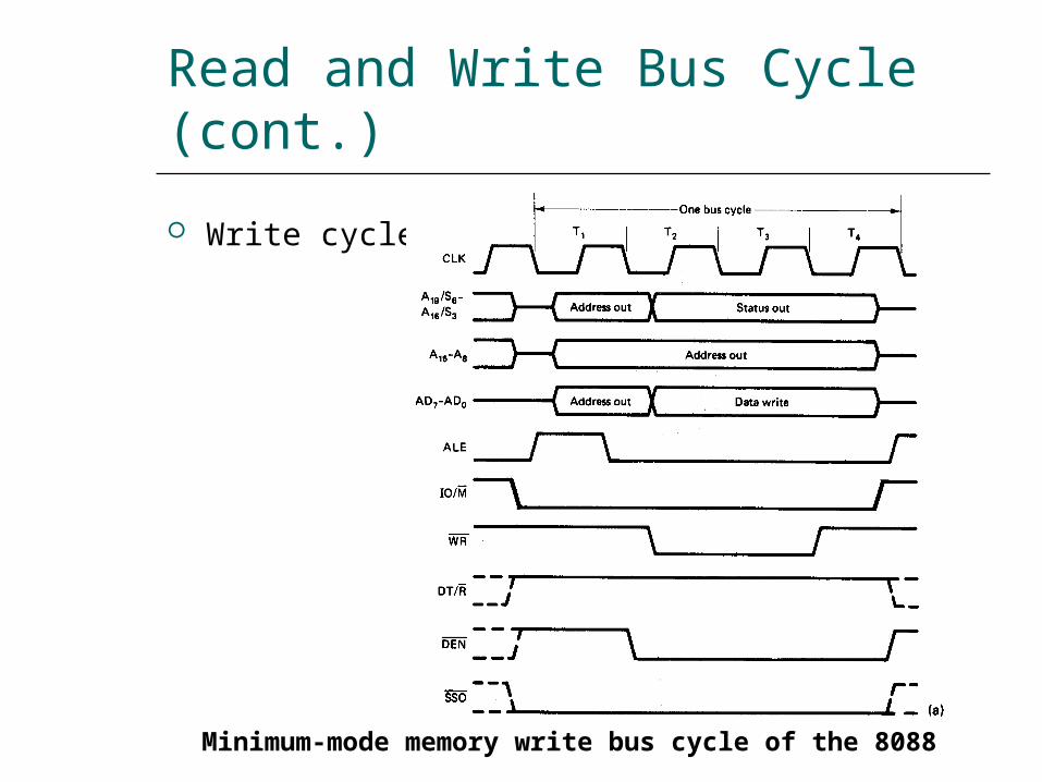
Memory Interface Circuit (cont)
Address bus latches and buffers
Circuit diagram of the 74F373
Memory Interface Circuit (cont)
A review of flip-floplatch logic
Positive edge-triggered D flip-flop
Memory Interface Circuit (cont)
A review of flip-floplatch logic
Positive edge-triggered JK flip-flop
Memory Interface Circuit (cont)
A review of flip-floplatch logic
D-type latch
Memory Interface Circuit (cont)
Address bus latches and buffers
Address latch circuit
Memory Interface Circuit (cont)
Bank write and bank read control logic
Bank write control logic Bank read control logic
Memory Interface Circuit (cont)
Data bus transceivers
Block diagram and circuit diagram of the 74F245 octal bus transceiver
Memory Interface Circuit (cont)
Data bus transceivers
Data bus transceiver circuit
Memory Interface Circuit (cont)
Address decoder
Address bus configuration with address decoding
Memory Interface Circuit (cont)
Address decoder
Block diagram and operation of the 74F139 decoder
Memory Interface Circuit (cont)
Address decoder
Circuit diagram of the 74F139 decoder
Memory Interface Circuit (cont)
Address decoder
Address decoder circuit using 74F139
Memory Interface Circuit (cont)
Address decoder
Block diagram and operation of the 74F138 decoder
Memory Interface Circuit (cont)
Address decoder
Circuit diagram of the 74F138 decoder
Memory Interface Circuit (cont)
Address decoder
Address decoder circuit using 74F138
Types of InputOutput
The IO system allows peripherals to provide data or receive results of processing the data Using IO ports
The 80888086 MPU can employ two types of IO Isolated IO Memory-mapped IO
They differ in how IO ports are mapped into the address space
Types of InputOutput (cont)
Isolated inputoutput When using isolated IO in a microcomputer
system the IO device are treated separate from memory
The memory address space contains 1 M consecutive byte address in the range 0000016 through FFFFF16
The IO address space contains 64K consecutive byte addresses in the range 000016 through FFFF16
The bytes in two consecutive IO addresses can be accessed as word-wide data
Page 0 000016 00FF16
Certain IO instructions can only perform in this range
Types of InputOutput (cont)
Isolated inputoutput
80888086 memory and IO address spaces
Types of InputOutput (cont)
Isolated inputoutput
Isolated IO ports
Types of InputOutput (cont)
Isolated inputoutput Advantages
The complete 1Mbyte memory address space is available for use with memory
Special instructions have been provided to perform IO operations with maximized performance
The bytes in two consecutive IO addresses can be accessed as word-wide data
Disadvantages All input and output data transfers must take place
between the AL or AX register and IO port
Types of InputOutput (cont)
Memory-mapped inputoutput MPU looks at the IO port as though it is a storage
location in memory Some of the memory address space is dedicated to IO
ports Instructions that affect data in memory are used
instead of the special IO instructions More instructions and addressing modes are available to
perform IO operations IO transfers can take place between IO port and other
internal registers The memory instructions tend to execute slower
than those specifically designed for isolated IO Part of the memory address space is lost
Types of InputOutput(cont)
Memory-mapped inputoutput
Memory mapped IO ports
Isolated InputOutput Interface
IO devices Keyboard Printer Mouse 82C55A etc
Functions of interface circuit Select the IO port Latch output data Sample input data Synchronize data transfer Translate between TTL voltage levels and those
required to operate the IO devices
Isolated InputOutput Interface (cont)
Minimum-mode interface
Minimum-mode 8088 system IO interface
Isolated InputOutput Interface (cont)
Minimum-mode interface
Minimum-mode 8086 system IO interface
Isolated InputOutput Interface (cont)
Maximum-mode interface
Maximum-mode 8088 system IO interface
Isolated InputOutput Interface (cont)
Maximum-mode interface
Maximum-mode 8086 system IO interface
Isolated InputOutput Interface (cont)
Maximum-mode interface
IO bus cycle status codes
InputOutput Data Transfer
Inputoutput data transfers in the 8088 and 8086 microcomputers can be either byte-wide or word-wide
IO addresses are 16 bits in length and are output by the 8088 to the IO interface over bus lines AD0 through AD7 and A8 through A15
In 8088 the word transfers is performed as two consecutive byte-wide data transfer and takes two bus cycle
In 8086 the word transfers can takes either one or two bus cycle
Word-wide IO ports should be aligned at even-address boundaries
InputOutput Data Instructions
InputOutput Data Instructions(cont)
EXAMPLE Write a sequence of instructions that will output
the data FF16 to a byte-wide output port at address AB16 of the IO address space
Solution First the AL register is loaded with FF16 as an
immediate operand in the instruction
MOV AL 0FFH Now the data in AL can be output to the byte-
wide output port with the instruction
OUT 0ABH AL
InputOutput Data Instructions(cont)
EXAMPLE Write a series of instructions that will output FF16 to an
output port located at address B00016 of the IO address space
Solution The DX register must first be loaded with the address
of the output port This is done with the instructionMOV DX 0B000H
Next the data that are to be output must be loaded into AL with the instruction
MOV AL 0FFH Finally the data are output with the instruction
OUT DX AL
InputOutput Data Instructions(cont)
EXAMPLE Data are to be read in from two byte-wide input
ports at addresses AA16 and A916 and then output as a word-wide output port at address B00016 Write a sequence of instructions to perform this inputoutput operation
InputOutput Data Instructions(cont)
Solution First read in the byte at address AA16 into AL and
move it into AHIN AL 0AAHMOV AH AL
Now the other byte can be read into AL by the instructionIN AL 09AH
And to write out the word of dataMOV DX 0B000HOUT DX AX
InputOutput Bus Cycles
Input bus cycle of the 8088
InputOutput Bus Cycles (cont)
Output bus cycle of the 8088
InputOutput Bus Cycles (cont)
Input bus cycle of the 8086
InputOutput Bus Cycles (cont)
Output bus cycle of the 8086
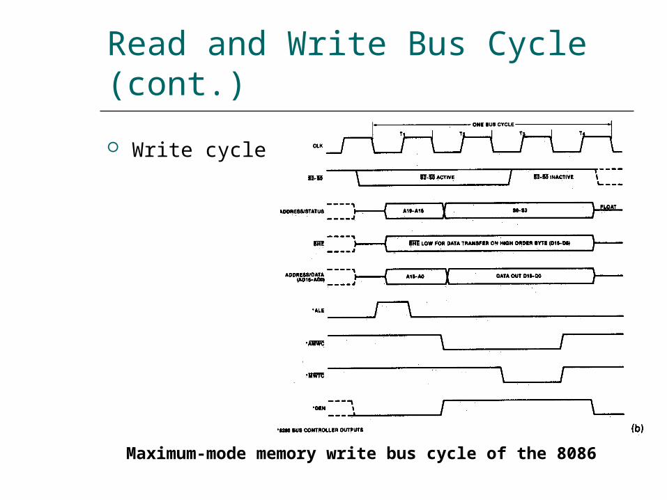
Memory Interface Circuit (cont)
A review of flip-floplatch logic
Positive edge-triggered D flip-flop
Memory Interface Circuit (cont)
A review of flip-floplatch logic
Positive edge-triggered JK flip-flop
Memory Interface Circuit (cont)
A review of flip-floplatch logic
D-type latch
Memory Interface Circuit (cont)
Address bus latches and buffers
Address latch circuit
Memory Interface Circuit (cont)
Bank write and bank read control logic
Bank write control logic Bank read control logic
Memory Interface Circuit (cont)
Data bus transceivers
Block diagram and circuit diagram of the 74F245 octal bus transceiver
Memory Interface Circuit (cont)
Data bus transceivers
Data bus transceiver circuit
Memory Interface Circuit (cont)
Address decoder
Address bus configuration with address decoding
Memory Interface Circuit (cont)
Address decoder
Block diagram and operation of the 74F139 decoder
Memory Interface Circuit (cont)
Address decoder
Circuit diagram of the 74F139 decoder
Memory Interface Circuit (cont)
Address decoder
Address decoder circuit using 74F139
Memory Interface Circuit (cont)
Address decoder
Block diagram and operation of the 74F138 decoder
Memory Interface Circuit (cont)
Address decoder
Circuit diagram of the 74F138 decoder
Memory Interface Circuit (cont)
Address decoder
Address decoder circuit using 74F138
Types of InputOutput
The IO system allows peripherals to provide data or receive results of processing the data Using IO ports
The 80888086 MPU can employ two types of IO Isolated IO Memory-mapped IO
They differ in how IO ports are mapped into the address space
Types of InputOutput (cont)
Isolated inputoutput When using isolated IO in a microcomputer
system the IO device are treated separate from memory
The memory address space contains 1 M consecutive byte address in the range 0000016 through FFFFF16
The IO address space contains 64K consecutive byte addresses in the range 000016 through FFFF16
The bytes in two consecutive IO addresses can be accessed as word-wide data
Page 0 000016 00FF16
Certain IO instructions can only perform in this range
Types of InputOutput (cont)
Isolated inputoutput
80888086 memory and IO address spaces
Types of InputOutput (cont)
Isolated inputoutput
Isolated IO ports
Types of InputOutput (cont)
Isolated inputoutput Advantages
The complete 1Mbyte memory address space is available for use with memory
Special instructions have been provided to perform IO operations with maximized performance
The bytes in two consecutive IO addresses can be accessed as word-wide data
Disadvantages All input and output data transfers must take place
between the AL or AX register and IO port
Types of InputOutput (cont)
Memory-mapped inputoutput MPU looks at the IO port as though it is a storage
location in memory Some of the memory address space is dedicated to IO
ports Instructions that affect data in memory are used
instead of the special IO instructions More instructions and addressing modes are available to
perform IO operations IO transfers can take place between IO port and other
internal registers The memory instructions tend to execute slower
than those specifically designed for isolated IO Part of the memory address space is lost
Types of InputOutput(cont)
Memory-mapped inputoutput
Memory mapped IO ports
Isolated InputOutput Interface
IO devices Keyboard Printer Mouse 82C55A etc
Functions of interface circuit Select the IO port Latch output data Sample input data Synchronize data transfer Translate between TTL voltage levels and those
required to operate the IO devices
Isolated InputOutput Interface (cont)
Minimum-mode interface
Minimum-mode 8088 system IO interface
Isolated InputOutput Interface (cont)
Minimum-mode interface
Minimum-mode 8086 system IO interface
Isolated InputOutput Interface (cont)
Maximum-mode interface
Maximum-mode 8088 system IO interface
Isolated InputOutput Interface (cont)
Maximum-mode interface
Maximum-mode 8086 system IO interface
Isolated InputOutput Interface (cont)
Maximum-mode interface
IO bus cycle status codes
InputOutput Data Transfer
Inputoutput data transfers in the 8088 and 8086 microcomputers can be either byte-wide or word-wide
IO addresses are 16 bits in length and are output by the 8088 to the IO interface over bus lines AD0 through AD7 and A8 through A15
In 8088 the word transfers is performed as two consecutive byte-wide data transfer and takes two bus cycle
In 8086 the word transfers can takes either one or two bus cycle
Word-wide IO ports should be aligned at even-address boundaries
InputOutput Data Instructions
InputOutput Data Instructions(cont)
EXAMPLE Write a sequence of instructions that will output
the data FF16 to a byte-wide output port at address AB16 of the IO address space
Solution First the AL register is loaded with FF16 as an
immediate operand in the instruction
MOV AL 0FFH Now the data in AL can be output to the byte-
wide output port with the instruction
OUT 0ABH AL
InputOutput Data Instructions(cont)
EXAMPLE Write a series of instructions that will output FF16 to an
output port located at address B00016 of the IO address space
Solution The DX register must first be loaded with the address
of the output port This is done with the instructionMOV DX 0B000H
Next the data that are to be output must be loaded into AL with the instruction
MOV AL 0FFH Finally the data are output with the instruction
OUT DX AL
InputOutput Data Instructions(cont)
EXAMPLE Data are to be read in from two byte-wide input
ports at addresses AA16 and A916 and then output as a word-wide output port at address B00016 Write a sequence of instructions to perform this inputoutput operation
InputOutput Data Instructions(cont)
Solution First read in the byte at address AA16 into AL and
move it into AHIN AL 0AAHMOV AH AL
Now the other byte can be read into AL by the instructionIN AL 09AH
And to write out the word of dataMOV DX 0B000HOUT DX AX
InputOutput Bus Cycles
Input bus cycle of the 8088
InputOutput Bus Cycles (cont)
Output bus cycle of the 8088
InputOutput Bus Cycles (cont)
Input bus cycle of the 8086
InputOutput Bus Cycles (cont)
Output bus cycle of the 8086
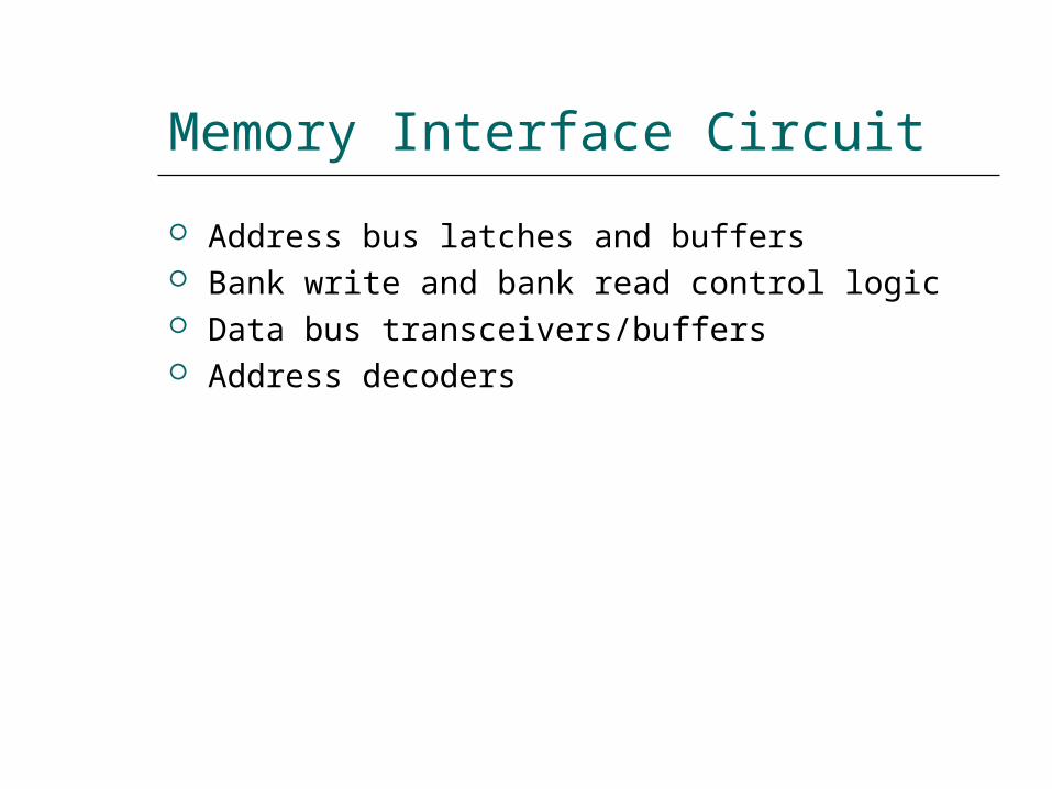
Memory Interface Circuit (cont)
A review of flip-floplatch logic
Positive edge-triggered JK flip-flop
Memory Interface Circuit (cont)
A review of flip-floplatch logic
D-type latch
Memory Interface Circuit (cont)
Address bus latches and buffers
Address latch circuit
Memory Interface Circuit (cont)
Bank write and bank read control logic
Bank write control logic Bank read control logic
Memory Interface Circuit (cont)
Data bus transceivers
Block diagram and circuit diagram of the 74F245 octal bus transceiver
Memory Interface Circuit (cont)
Data bus transceivers
Data bus transceiver circuit
Memory Interface Circuit (cont)
Address decoder
Address bus configuration with address decoding
Memory Interface Circuit (cont)
Address decoder
Block diagram and operation of the 74F139 decoder
Memory Interface Circuit (cont)
Address decoder
Circuit diagram of the 74F139 decoder
Memory Interface Circuit (cont)
Address decoder
Address decoder circuit using 74F139
Memory Interface Circuit (cont)
Address decoder
Block diagram and operation of the 74F138 decoder
Memory Interface Circuit (cont)
Address decoder
Circuit diagram of the 74F138 decoder
Memory Interface Circuit (cont)
Address decoder
Address decoder circuit using 74F138
Types of InputOutput
The IO system allows peripherals to provide data or receive results of processing the data Using IO ports
The 80888086 MPU can employ two types of IO Isolated IO Memory-mapped IO
They differ in how IO ports are mapped into the address space
Types of InputOutput (cont)
Isolated inputoutput When using isolated IO in a microcomputer
system the IO device are treated separate from memory
The memory address space contains 1 M consecutive byte address in the range 0000016 through FFFFF16
The IO address space contains 64K consecutive byte addresses in the range 000016 through FFFF16
The bytes in two consecutive IO addresses can be accessed as word-wide data
Page 0 000016 00FF16
Certain IO instructions can only perform in this range
Types of InputOutput (cont)
Isolated inputoutput
80888086 memory and IO address spaces
Types of InputOutput (cont)
Isolated inputoutput
Isolated IO ports
Types of InputOutput (cont)
Isolated inputoutput Advantages
The complete 1Mbyte memory address space is available for use with memory
Special instructions have been provided to perform IO operations with maximized performance
The bytes in two consecutive IO addresses can be accessed as word-wide data
Disadvantages All input and output data transfers must take place
between the AL or AX register and IO port
Types of InputOutput (cont)
Memory-mapped inputoutput MPU looks at the IO port as though it is a storage
location in memory Some of the memory address space is dedicated to IO
ports Instructions that affect data in memory are used
instead of the special IO instructions More instructions and addressing modes are available to
perform IO operations IO transfers can take place between IO port and other
internal registers The memory instructions tend to execute slower
than those specifically designed for isolated IO Part of the memory address space is lost
Types of InputOutput(cont)
Memory-mapped inputoutput
Memory mapped IO ports
Isolated InputOutput Interface
IO devices Keyboard Printer Mouse 82C55A etc
Functions of interface circuit Select the IO port Latch output data Sample input data Synchronize data transfer Translate between TTL voltage levels and those
required to operate the IO devices
Isolated InputOutput Interface (cont)
Minimum-mode interface
Minimum-mode 8088 system IO interface
Isolated InputOutput Interface (cont)
Minimum-mode interface
Minimum-mode 8086 system IO interface
Isolated InputOutput Interface (cont)
Maximum-mode interface
Maximum-mode 8088 system IO interface
Isolated InputOutput Interface (cont)
Maximum-mode interface
Maximum-mode 8086 system IO interface
Isolated InputOutput Interface (cont)
Maximum-mode interface
IO bus cycle status codes
InputOutput Data Transfer
Inputoutput data transfers in the 8088 and 8086 microcomputers can be either byte-wide or word-wide
IO addresses are 16 bits in length and are output by the 8088 to the IO interface over bus lines AD0 through AD7 and A8 through A15
In 8088 the word transfers is performed as two consecutive byte-wide data transfer and takes two bus cycle
In 8086 the word transfers can takes either one or two bus cycle
Word-wide IO ports should be aligned at even-address boundaries
InputOutput Data Instructions
InputOutput Data Instructions(cont)
EXAMPLE Write a sequence of instructions that will output
the data FF16 to a byte-wide output port at address AB16 of the IO address space
Solution First the AL register is loaded with FF16 as an
immediate operand in the instruction
MOV AL 0FFH Now the data in AL can be output to the byte-
wide output port with the instruction
OUT 0ABH AL
InputOutput Data Instructions(cont)
EXAMPLE Write a series of instructions that will output FF16 to an
output port located at address B00016 of the IO address space
Solution The DX register must first be loaded with the address
of the output port This is done with the instructionMOV DX 0B000H
Next the data that are to be output must be loaded into AL with the instruction
MOV AL 0FFH Finally the data are output with the instruction
OUT DX AL
InputOutput Data Instructions(cont)
EXAMPLE Data are to be read in from two byte-wide input
ports at addresses AA16 and A916 and then output as a word-wide output port at address B00016 Write a sequence of instructions to perform this inputoutput operation
InputOutput Data Instructions(cont)
Solution First read in the byte at address AA16 into AL and
move it into AHIN AL 0AAHMOV AH AL
Now the other byte can be read into AL by the instructionIN AL 09AH
And to write out the word of dataMOV DX 0B000HOUT DX AX
InputOutput Bus Cycles
Input bus cycle of the 8088
InputOutput Bus Cycles (cont)
Output bus cycle of the 8088
InputOutput Bus Cycles (cont)
Input bus cycle of the 8086
InputOutput Bus Cycles (cont)
Output bus cycle of the 8086
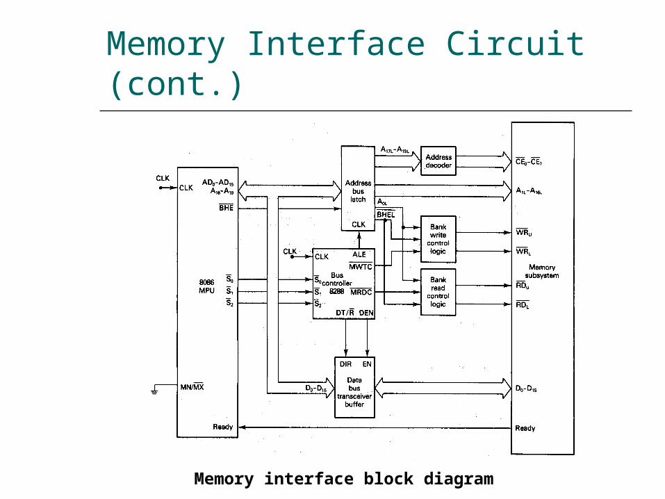
Memory Interface Circuit (cont)
A review of flip-floplatch logic
D-type latch
Memory Interface Circuit (cont)
Address bus latches and buffers
Address latch circuit
Memory Interface Circuit (cont)
Bank write and bank read control logic
Bank write control logic Bank read control logic
Memory Interface Circuit (cont)
Data bus transceivers
Block diagram and circuit diagram of the 74F245 octal bus transceiver
Memory Interface Circuit (cont)
Data bus transceivers
Data bus transceiver circuit
Memory Interface Circuit (cont)
Address decoder
Address bus configuration with address decoding
Memory Interface Circuit (cont)
Address decoder
Block diagram and operation of the 74F139 decoder
Memory Interface Circuit (cont)
Address decoder
Circuit diagram of the 74F139 decoder
Memory Interface Circuit (cont)
Address decoder
Address decoder circuit using 74F139
Memory Interface Circuit (cont)
Address decoder
Block diagram and operation of the 74F138 decoder
Memory Interface Circuit (cont)
Address decoder
Circuit diagram of the 74F138 decoder
Memory Interface Circuit (cont)
Address decoder
Address decoder circuit using 74F138
Types of InputOutput
The IO system allows peripherals to provide data or receive results of processing the data Using IO ports
The 80888086 MPU can employ two types of IO Isolated IO Memory-mapped IO
They differ in how IO ports are mapped into the address space
Types of InputOutput (cont)
Isolated inputoutput When using isolated IO in a microcomputer
system the IO device are treated separate from memory
The memory address space contains 1 M consecutive byte address in the range 0000016 through FFFFF16
The IO address space contains 64K consecutive byte addresses in the range 000016 through FFFF16
The bytes in two consecutive IO addresses can be accessed as word-wide data
Page 0 000016 00FF16
Certain IO instructions can only perform in this range
Types of InputOutput (cont)
Isolated inputoutput
80888086 memory and IO address spaces
Types of InputOutput (cont)
Isolated inputoutput
Isolated IO ports
Types of InputOutput (cont)
Isolated inputoutput Advantages
The complete 1Mbyte memory address space is available for use with memory
Special instructions have been provided to perform IO operations with maximized performance
The bytes in two consecutive IO addresses can be accessed as word-wide data
Disadvantages All input and output data transfers must take place
between the AL or AX register and IO port
Types of InputOutput (cont)
Memory-mapped inputoutput MPU looks at the IO port as though it is a storage
location in memory Some of the memory address space is dedicated to IO
ports Instructions that affect data in memory are used
instead of the special IO instructions More instructions and addressing modes are available to
perform IO operations IO transfers can take place between IO port and other
internal registers The memory instructions tend to execute slower
than those specifically designed for isolated IO Part of the memory address space is lost
Types of InputOutput(cont)
Memory-mapped inputoutput
Memory mapped IO ports
Isolated InputOutput Interface
IO devices Keyboard Printer Mouse 82C55A etc
Functions of interface circuit Select the IO port Latch output data Sample input data Synchronize data transfer Translate between TTL voltage levels and those
required to operate the IO devices
Isolated InputOutput Interface (cont)
Minimum-mode interface
Minimum-mode 8088 system IO interface
Isolated InputOutput Interface (cont)
Minimum-mode interface
Minimum-mode 8086 system IO interface
Isolated InputOutput Interface (cont)
Maximum-mode interface
Maximum-mode 8088 system IO interface
Isolated InputOutput Interface (cont)
Maximum-mode interface
Maximum-mode 8086 system IO interface
Isolated InputOutput Interface (cont)
Maximum-mode interface
IO bus cycle status codes
InputOutput Data Transfer
Inputoutput data transfers in the 8088 and 8086 microcomputers can be either byte-wide or word-wide
IO addresses are 16 bits in length and are output by the 8088 to the IO interface over bus lines AD0 through AD7 and A8 through A15
In 8088 the word transfers is performed as two consecutive byte-wide data transfer and takes two bus cycle
In 8086 the word transfers can takes either one or two bus cycle
Word-wide IO ports should be aligned at even-address boundaries
InputOutput Data Instructions
InputOutput Data Instructions(cont)
EXAMPLE Write a sequence of instructions that will output
the data FF16 to a byte-wide output port at address AB16 of the IO address space
Solution First the AL register is loaded with FF16 as an
immediate operand in the instruction
MOV AL 0FFH Now the data in AL can be output to the byte-
wide output port with the instruction
OUT 0ABH AL
InputOutput Data Instructions(cont)
EXAMPLE Write a series of instructions that will output FF16 to an
output port located at address B00016 of the IO address space
Solution The DX register must first be loaded with the address
of the output port This is done with the instructionMOV DX 0B000H
Next the data that are to be output must be loaded into AL with the instruction
MOV AL 0FFH Finally the data are output with the instruction
OUT DX AL
InputOutput Data Instructions(cont)
EXAMPLE Data are to be read in from two byte-wide input
ports at addresses AA16 and A916 and then output as a word-wide output port at address B00016 Write a sequence of instructions to perform this inputoutput operation
InputOutput Data Instructions(cont)
Solution First read in the byte at address AA16 into AL and
move it into AHIN AL 0AAHMOV AH AL
Now the other byte can be read into AL by the instructionIN AL 09AH
And to write out the word of dataMOV DX 0B000HOUT DX AX
InputOutput Bus Cycles
Input bus cycle of the 8088
InputOutput Bus Cycles (cont)
Output bus cycle of the 8088
InputOutput Bus Cycles (cont)
Input bus cycle of the 8086
InputOutput Bus Cycles (cont)
Output bus cycle of the 8086
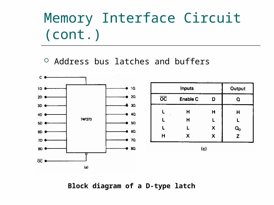
Memory Interface Circuit (cont)
Address bus latches and buffers
Address latch circuit
Memory Interface Circuit (cont)
Bank write and bank read control logic
Bank write control logic Bank read control logic
Memory Interface Circuit (cont)
Data bus transceivers
Block diagram and circuit diagram of the 74F245 octal bus transceiver
Memory Interface Circuit (cont)
Data bus transceivers
Data bus transceiver circuit
Memory Interface Circuit (cont)
Address decoder
Address bus configuration with address decoding
Memory Interface Circuit (cont)
Address decoder
Block diagram and operation of the 74F139 decoder
Memory Interface Circuit (cont)
Address decoder
Circuit diagram of the 74F139 decoder
Memory Interface Circuit (cont)
Address decoder
Address decoder circuit using 74F139
Memory Interface Circuit (cont)
Address decoder
Block diagram and operation of the 74F138 decoder
Memory Interface Circuit (cont)
Address decoder
Circuit diagram of the 74F138 decoder
Memory Interface Circuit (cont)
Address decoder
Address decoder circuit using 74F138
Types of InputOutput
The IO system allows peripherals to provide data or receive results of processing the data Using IO ports
The 80888086 MPU can employ two types of IO Isolated IO Memory-mapped IO
They differ in how IO ports are mapped into the address space
Types of InputOutput (cont)
Isolated inputoutput When using isolated IO in a microcomputer
system the IO device are treated separate from memory
The memory address space contains 1 M consecutive byte address in the range 0000016 through FFFFF16
The IO address space contains 64K consecutive byte addresses in the range 000016 through FFFF16
The bytes in two consecutive IO addresses can be accessed as word-wide data
Page 0 000016 00FF16
Certain IO instructions can only perform in this range
Types of InputOutput (cont)
Isolated inputoutput
80888086 memory and IO address spaces
Types of InputOutput (cont)
Isolated inputoutput
Isolated IO ports
Types of InputOutput (cont)
Isolated inputoutput Advantages
The complete 1Mbyte memory address space is available for use with memory
Special instructions have been provided to perform IO operations with maximized performance
The bytes in two consecutive IO addresses can be accessed as word-wide data
Disadvantages All input and output data transfers must take place
between the AL or AX register and IO port
Types of InputOutput (cont)
Memory-mapped inputoutput MPU looks at the IO port as though it is a storage
location in memory Some of the memory address space is dedicated to IO
ports Instructions that affect data in memory are used
instead of the special IO instructions More instructions and addressing modes are available to
perform IO operations IO transfers can take place between IO port and other
internal registers The memory instructions tend to execute slower
than those specifically designed for isolated IO Part of the memory address space is lost
Types of InputOutput(cont)
Memory-mapped inputoutput
Memory mapped IO ports
Isolated InputOutput Interface
IO devices Keyboard Printer Mouse 82C55A etc
Functions of interface circuit Select the IO port Latch output data Sample input data Synchronize data transfer Translate between TTL voltage levels and those
required to operate the IO devices
Isolated InputOutput Interface (cont)
Minimum-mode interface
Minimum-mode 8088 system IO interface
Isolated InputOutput Interface (cont)
Minimum-mode interface
Minimum-mode 8086 system IO interface
Isolated InputOutput Interface (cont)
Maximum-mode interface
Maximum-mode 8088 system IO interface
Isolated InputOutput Interface (cont)
Maximum-mode interface
Maximum-mode 8086 system IO interface
Isolated InputOutput Interface (cont)
Maximum-mode interface
IO bus cycle status codes
InputOutput Data Transfer
Inputoutput data transfers in the 8088 and 8086 microcomputers can be either byte-wide or word-wide
IO addresses are 16 bits in length and are output by the 8088 to the IO interface over bus lines AD0 through AD7 and A8 through A15
In 8088 the word transfers is performed as two consecutive byte-wide data transfer and takes two bus cycle
In 8086 the word transfers can takes either one or two bus cycle
Word-wide IO ports should be aligned at even-address boundaries
InputOutput Data Instructions
InputOutput Data Instructions(cont)
EXAMPLE Write a sequence of instructions that will output
the data FF16 to a byte-wide output port at address AB16 of the IO address space
Solution First the AL register is loaded with FF16 as an
immediate operand in the instruction
MOV AL 0FFH Now the data in AL can be output to the byte-
wide output port with the instruction
OUT 0ABH AL
InputOutput Data Instructions(cont)
EXAMPLE Write a series of instructions that will output FF16 to an
output port located at address B00016 of the IO address space
Solution The DX register must first be loaded with the address
of the output port This is done with the instructionMOV DX 0B000H
Next the data that are to be output must be loaded into AL with the instruction
MOV AL 0FFH Finally the data are output with the instruction
OUT DX AL
InputOutput Data Instructions(cont)
EXAMPLE Data are to be read in from two byte-wide input
ports at addresses AA16 and A916 and then output as a word-wide output port at address B00016 Write a sequence of instructions to perform this inputoutput operation
InputOutput Data Instructions(cont)
Solution First read in the byte at address AA16 into AL and
move it into AHIN AL 0AAHMOV AH AL
Now the other byte can be read into AL by the instructionIN AL 09AH
And to write out the word of dataMOV DX 0B000HOUT DX AX
InputOutput Bus Cycles
Input bus cycle of the 8088
InputOutput Bus Cycles (cont)
Output bus cycle of the 8088
InputOutput Bus Cycles (cont)
Input bus cycle of the 8086
InputOutput Bus Cycles (cont)
Output bus cycle of the 8086
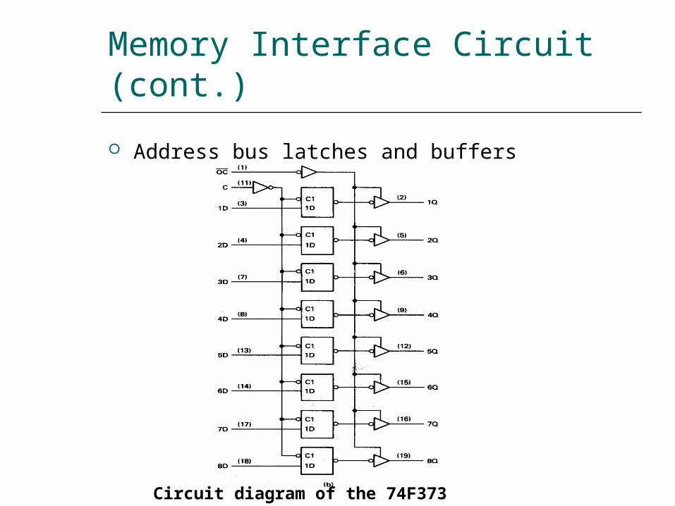
Memory Interface Circuit (cont)
Bank write and bank read control logic
Bank write control logic Bank read control logic
Memory Interface Circuit (cont)
Data bus transceivers
Block diagram and circuit diagram of the 74F245 octal bus transceiver
Memory Interface Circuit (cont)
Data bus transceivers
Data bus transceiver circuit
Memory Interface Circuit (cont)
Address decoder
Address bus configuration with address decoding
Memory Interface Circuit (cont)
Address decoder
Block diagram and operation of the 74F139 decoder
Memory Interface Circuit (cont)
Address decoder
Circuit diagram of the 74F139 decoder
Memory Interface Circuit (cont)
Address decoder
Address decoder circuit using 74F139
Memory Interface Circuit (cont)
Address decoder
Block diagram and operation of the 74F138 decoder
Memory Interface Circuit (cont)
Address decoder
Circuit diagram of the 74F138 decoder
Memory Interface Circuit (cont)
Address decoder
Address decoder circuit using 74F138
Types of InputOutput
The IO system allows peripherals to provide data or receive results of processing the data Using IO ports
The 80888086 MPU can employ two types of IO Isolated IO Memory-mapped IO
They differ in how IO ports are mapped into the address space
Types of InputOutput (cont)
Isolated inputoutput When using isolated IO in a microcomputer
system the IO device are treated separate from memory
The memory address space contains 1 M consecutive byte address in the range 0000016 through FFFFF16
The IO address space contains 64K consecutive byte addresses in the range 000016 through FFFF16
The bytes in two consecutive IO addresses can be accessed as word-wide data
Page 0 000016 00FF16
Certain IO instructions can only perform in this range
Types of InputOutput (cont)
Isolated inputoutput
80888086 memory and IO address spaces
Types of InputOutput (cont)
Isolated inputoutput
Isolated IO ports
Types of InputOutput (cont)
Isolated inputoutput Advantages
The complete 1Mbyte memory address space is available for use with memory
Special instructions have been provided to perform IO operations with maximized performance
The bytes in two consecutive IO addresses can be accessed as word-wide data
Disadvantages All input and output data transfers must take place
between the AL or AX register and IO port
Types of InputOutput (cont)
Memory-mapped inputoutput MPU looks at the IO port as though it is a storage
location in memory Some of the memory address space is dedicated to IO
ports Instructions that affect data in memory are used
instead of the special IO instructions More instructions and addressing modes are available to
perform IO operations IO transfers can take place between IO port and other
internal registers The memory instructions tend to execute slower
than those specifically designed for isolated IO Part of the memory address space is lost
Types of InputOutput(cont)
Memory-mapped inputoutput
Memory mapped IO ports
Isolated InputOutput Interface
IO devices Keyboard Printer Mouse 82C55A etc
Functions of interface circuit Select the IO port Latch output data Sample input data Synchronize data transfer Translate between TTL voltage levels and those
required to operate the IO devices
Isolated InputOutput Interface (cont)
Minimum-mode interface
Minimum-mode 8088 system IO interface
Isolated InputOutput Interface (cont)
Minimum-mode interface
Minimum-mode 8086 system IO interface
Isolated InputOutput Interface (cont)
Maximum-mode interface
Maximum-mode 8088 system IO interface
Isolated InputOutput Interface (cont)
Maximum-mode interface
Maximum-mode 8086 system IO interface
Isolated InputOutput Interface (cont)
Maximum-mode interface
IO bus cycle status codes
InputOutput Data Transfer
Inputoutput data transfers in the 8088 and 8086 microcomputers can be either byte-wide or word-wide
IO addresses are 16 bits in length and are output by the 8088 to the IO interface over bus lines AD0 through AD7 and A8 through A15
In 8088 the word transfers is performed as two consecutive byte-wide data transfer and takes two bus cycle
In 8086 the word transfers can takes either one or two bus cycle
Word-wide IO ports should be aligned at even-address boundaries
InputOutput Data Instructions
InputOutput Data Instructions(cont)
EXAMPLE Write a sequence of instructions that will output
the data FF16 to a byte-wide output port at address AB16 of the IO address space
Solution First the AL register is loaded with FF16 as an
immediate operand in the instruction
MOV AL 0FFH Now the data in AL can be output to the byte-
wide output port with the instruction
OUT 0ABH AL
InputOutput Data Instructions(cont)
EXAMPLE Write a series of instructions that will output FF16 to an
output port located at address B00016 of the IO address space
Solution The DX register must first be loaded with the address
of the output port This is done with the instructionMOV DX 0B000H
Next the data that are to be output must be loaded into AL with the instruction
MOV AL 0FFH Finally the data are output with the instruction
OUT DX AL
InputOutput Data Instructions(cont)
EXAMPLE Data are to be read in from two byte-wide input
ports at addresses AA16 and A916 and then output as a word-wide output port at address B00016 Write a sequence of instructions to perform this inputoutput operation
InputOutput Data Instructions(cont)
Solution First read in the byte at address AA16 into AL and
move it into AHIN AL 0AAHMOV AH AL
Now the other byte can be read into AL by the instructionIN AL 09AH
And to write out the word of dataMOV DX 0B000HOUT DX AX
InputOutput Bus Cycles
Input bus cycle of the 8088
InputOutput Bus Cycles (cont)
Output bus cycle of the 8088
InputOutput Bus Cycles (cont)
Input bus cycle of the 8086
InputOutput Bus Cycles (cont)
Output bus cycle of the 8086
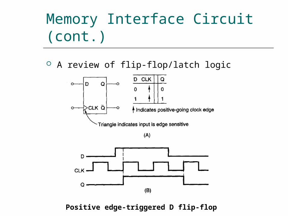
Memory Interface Circuit (cont)
Data bus transceivers
Block diagram and circuit diagram of the 74F245 octal bus transceiver
Memory Interface Circuit (cont)
Data bus transceivers
Data bus transceiver circuit
Memory Interface Circuit (cont)
Address decoder
Address bus configuration with address decoding
Memory Interface Circuit (cont)
Address decoder
Block diagram and operation of the 74F139 decoder
Memory Interface Circuit (cont)
Address decoder
Circuit diagram of the 74F139 decoder
Memory Interface Circuit (cont)
Address decoder
Address decoder circuit using 74F139
Memory Interface Circuit (cont)
Address decoder
Block diagram and operation of the 74F138 decoder
Memory Interface Circuit (cont)
Address decoder
Circuit diagram of the 74F138 decoder
Memory Interface Circuit (cont)
Address decoder
Address decoder circuit using 74F138
Types of InputOutput
The IO system allows peripherals to provide data or receive results of processing the data Using IO ports
The 80888086 MPU can employ two types of IO Isolated IO Memory-mapped IO
They differ in how IO ports are mapped into the address space
Types of InputOutput (cont)
Isolated inputoutput When using isolated IO in a microcomputer
system the IO device are treated separate from memory
The memory address space contains 1 M consecutive byte address in the range 0000016 through FFFFF16
The IO address space contains 64K consecutive byte addresses in the range 000016 through FFFF16
The bytes in two consecutive IO addresses can be accessed as word-wide data
Page 0 000016 00FF16
Certain IO instructions can only perform in this range
Types of InputOutput (cont)
Isolated inputoutput
80888086 memory and IO address spaces
Types of InputOutput (cont)
Isolated inputoutput
Isolated IO ports
Types of InputOutput (cont)
Isolated inputoutput Advantages
The complete 1Mbyte memory address space is available for use with memory
Special instructions have been provided to perform IO operations with maximized performance
The bytes in two consecutive IO addresses can be accessed as word-wide data
Disadvantages All input and output data transfers must take place
between the AL or AX register and IO port
Types of InputOutput (cont)
Memory-mapped inputoutput MPU looks at the IO port as though it is a storage
location in memory Some of the memory address space is dedicated to IO
ports Instructions that affect data in memory are used
instead of the special IO instructions More instructions and addressing modes are available to
perform IO operations IO transfers can take place between IO port and other
internal registers The memory instructions tend to execute slower
than those specifically designed for isolated IO Part of the memory address space is lost
Types of InputOutput(cont)
Memory-mapped inputoutput
Memory mapped IO ports
Isolated InputOutput Interface
IO devices Keyboard Printer Mouse 82C55A etc
Functions of interface circuit Select the IO port Latch output data Sample input data Synchronize data transfer Translate between TTL voltage levels and those
required to operate the IO devices
Isolated InputOutput Interface (cont)
Minimum-mode interface
Minimum-mode 8088 system IO interface
Isolated InputOutput Interface (cont)
Minimum-mode interface
Minimum-mode 8086 system IO interface
Isolated InputOutput Interface (cont)
Maximum-mode interface
Maximum-mode 8088 system IO interface
Isolated InputOutput Interface (cont)
Maximum-mode interface
Maximum-mode 8086 system IO interface
Isolated InputOutput Interface (cont)
Maximum-mode interface
IO bus cycle status codes
InputOutput Data Transfer
Inputoutput data transfers in the 8088 and 8086 microcomputers can be either byte-wide or word-wide
IO addresses are 16 bits in length and are output by the 8088 to the IO interface over bus lines AD0 through AD7 and A8 through A15
In 8088 the word transfers is performed as two consecutive byte-wide data transfer and takes two bus cycle
In 8086 the word transfers can takes either one or two bus cycle
Word-wide IO ports should be aligned at even-address boundaries
InputOutput Data Instructions
InputOutput Data Instructions(cont)
EXAMPLE Write a sequence of instructions that will output
the data FF16 to a byte-wide output port at address AB16 of the IO address space
Solution First the AL register is loaded with FF16 as an
immediate operand in the instruction
MOV AL 0FFH Now the data in AL can be output to the byte-
wide output port with the instruction
OUT 0ABH AL
InputOutput Data Instructions(cont)
EXAMPLE Write a series of instructions that will output FF16 to an
output port located at address B00016 of the IO address space
Solution The DX register must first be loaded with the address
of the output port This is done with the instructionMOV DX 0B000H
Next the data that are to be output must be loaded into AL with the instruction
MOV AL 0FFH Finally the data are output with the instruction
OUT DX AL
InputOutput Data Instructions(cont)
EXAMPLE Data are to be read in from two byte-wide input
ports at addresses AA16 and A916 and then output as a word-wide output port at address B00016 Write a sequence of instructions to perform this inputoutput operation
InputOutput Data Instructions(cont)
Solution First read in the byte at address AA16 into AL and
move it into AHIN AL 0AAHMOV AH AL
Now the other byte can be read into AL by the instructionIN AL 09AH
And to write out the word of dataMOV DX 0B000HOUT DX AX
InputOutput Bus Cycles
Input bus cycle of the 8088
InputOutput Bus Cycles (cont)
Output bus cycle of the 8088
InputOutput Bus Cycles (cont)
Input bus cycle of the 8086
InputOutput Bus Cycles (cont)
Output bus cycle of the 8086
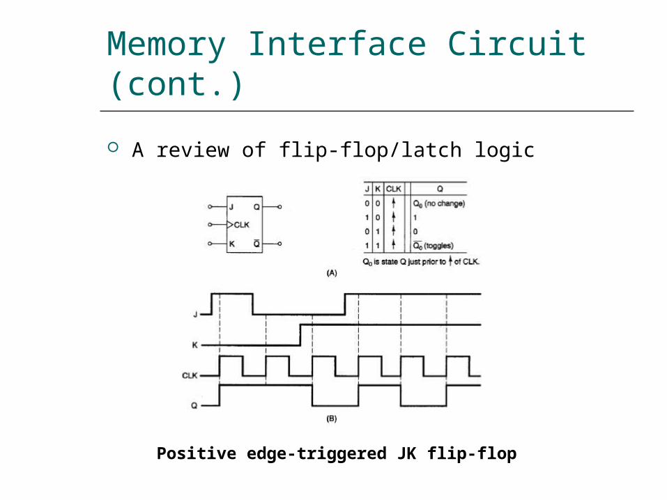
Memory Interface Circuit (cont)
Data bus transceivers
Data bus transceiver circuit
Memory Interface Circuit (cont)
Address decoder
Address bus configuration with address decoding
Memory Interface Circuit (cont)
Address decoder
Block diagram and operation of the 74F139 decoder
Memory Interface Circuit (cont)
Address decoder
Circuit diagram of the 74F139 decoder
Memory Interface Circuit (cont)
Address decoder
Address decoder circuit using 74F139
Memory Interface Circuit (cont)
Address decoder
Block diagram and operation of the 74F138 decoder
Memory Interface Circuit (cont)
Address decoder
Circuit diagram of the 74F138 decoder
Memory Interface Circuit (cont)
Address decoder
Address decoder circuit using 74F138
Types of InputOutput
The IO system allows peripherals to provide data or receive results of processing the data Using IO ports
The 80888086 MPU can employ two types of IO Isolated IO Memory-mapped IO
They differ in how IO ports are mapped into the address space
Types of InputOutput (cont)
Isolated inputoutput When using isolated IO in a microcomputer
system the IO device are treated separate from memory
The memory address space contains 1 M consecutive byte address in the range 0000016 through FFFFF16
The IO address space contains 64K consecutive byte addresses in the range 000016 through FFFF16
The bytes in two consecutive IO addresses can be accessed as word-wide data
Page 0 000016 00FF16
Certain IO instructions can only perform in this range
Types of InputOutput (cont)
Isolated inputoutput
80888086 memory and IO address spaces
Types of InputOutput (cont)
Isolated inputoutput
Isolated IO ports
Types of InputOutput (cont)
Isolated inputoutput Advantages
The complete 1Mbyte memory address space is available for use with memory
Special instructions have been provided to perform IO operations with maximized performance
The bytes in two consecutive IO addresses can be accessed as word-wide data
Disadvantages All input and output data transfers must take place
between the AL or AX register and IO port
Types of InputOutput (cont)
Memory-mapped inputoutput MPU looks at the IO port as though it is a storage
location in memory Some of the memory address space is dedicated to IO
ports Instructions that affect data in memory are used
instead of the special IO instructions More instructions and addressing modes are available to
perform IO operations IO transfers can take place between IO port and other
internal registers The memory instructions tend to execute slower
than those specifically designed for isolated IO Part of the memory address space is lost
Types of InputOutput(cont)
Memory-mapped inputoutput
Memory mapped IO ports
Isolated InputOutput Interface
IO devices Keyboard Printer Mouse 82C55A etc
Functions of interface circuit Select the IO port Latch output data Sample input data Synchronize data transfer Translate between TTL voltage levels and those
required to operate the IO devices
Isolated InputOutput Interface (cont)
Minimum-mode interface
Minimum-mode 8088 system IO interface
Isolated InputOutput Interface (cont)
Minimum-mode interface
Minimum-mode 8086 system IO interface
Isolated InputOutput Interface (cont)
Maximum-mode interface
Maximum-mode 8088 system IO interface
Isolated InputOutput Interface (cont)
Maximum-mode interface
Maximum-mode 8086 system IO interface
Isolated InputOutput Interface (cont)
Maximum-mode interface
IO bus cycle status codes
InputOutput Data Transfer
Inputoutput data transfers in the 8088 and 8086 microcomputers can be either byte-wide or word-wide
IO addresses are 16 bits in length and are output by the 8088 to the IO interface over bus lines AD0 through AD7 and A8 through A15
In 8088 the word transfers is performed as two consecutive byte-wide data transfer and takes two bus cycle
In 8086 the word transfers can takes either one or two bus cycle
Word-wide IO ports should be aligned at even-address boundaries
InputOutput Data Instructions
InputOutput Data Instructions(cont)
EXAMPLE Write a sequence of instructions that will output
the data FF16 to a byte-wide output port at address AB16 of the IO address space
Solution First the AL register is loaded with FF16 as an
immediate operand in the instruction
MOV AL 0FFH Now the data in AL can be output to the byte-
wide output port with the instruction
OUT 0ABH AL
InputOutput Data Instructions(cont)
EXAMPLE Write a series of instructions that will output FF16 to an
output port located at address B00016 of the IO address space
Solution The DX register must first be loaded with the address
of the output port This is done with the instructionMOV DX 0B000H
Next the data that are to be output must be loaded into AL with the instruction
MOV AL 0FFH Finally the data are output with the instruction
OUT DX AL
InputOutput Data Instructions(cont)
EXAMPLE Data are to be read in from two byte-wide input
ports at addresses AA16 and A916 and then output as a word-wide output port at address B00016 Write a sequence of instructions to perform this inputoutput operation
InputOutput Data Instructions(cont)
Solution First read in the byte at address AA16 into AL and
move it into AHIN AL 0AAHMOV AH AL
Now the other byte can be read into AL by the instructionIN AL 09AH
And to write out the word of dataMOV DX 0B000HOUT DX AX
InputOutput Bus Cycles
Input bus cycle of the 8088
InputOutput Bus Cycles (cont)
Output bus cycle of the 8088
InputOutput Bus Cycles (cont)
Input bus cycle of the 8086
InputOutput Bus Cycles (cont)
Output bus cycle of the 8086

Memory Interface Circuit (cont)
Address decoder
Block diagram and operation of the 74F139 decoder
Memory Interface Circuit (cont)
Address decoder
Circuit diagram of the 74F139 decoder
Memory Interface Circuit (cont)
Address decoder
Address decoder circuit using 74F139
Memory Interface Circuit (cont)
Address decoder
Block diagram and operation of the 74F138 decoder
Memory Interface Circuit (cont)
Address decoder
Circuit diagram of the 74F138 decoder
Memory Interface Circuit (cont)
Address decoder
Address decoder circuit using 74F138
Types of InputOutput
The IO system allows peripherals to provide data or receive results of processing the data Using IO ports
The 80888086 MPU can employ two types of IO Isolated IO Memory-mapped IO
They differ in how IO ports are mapped into the address space
Types of InputOutput (cont)
Isolated inputoutput When using isolated IO in a microcomputer
system the IO device are treated separate from memory
The memory address space contains 1 M consecutive byte address in the range 0000016 through FFFFF16
The IO address space contains 64K consecutive byte addresses in the range 000016 through FFFF16
The bytes in two consecutive IO addresses can be accessed as word-wide data
Page 0 000016 00FF16
Certain IO instructions can only perform in this range
Types of InputOutput (cont)
Isolated inputoutput
80888086 memory and IO address spaces
Types of InputOutput (cont)
Isolated inputoutput
Isolated IO ports
Types of InputOutput (cont)
Isolated inputoutput Advantages
The complete 1Mbyte memory address space is available for use with memory
Special instructions have been provided to perform IO operations with maximized performance
The bytes in two consecutive IO addresses can be accessed as word-wide data
Disadvantages All input and output data transfers must take place
between the AL or AX register and IO port
Types of InputOutput (cont)
Memory-mapped inputoutput MPU looks at the IO port as though it is a storage
location in memory Some of the memory address space is dedicated to IO
ports Instructions that affect data in memory are used
instead of the special IO instructions More instructions and addressing modes are available to
perform IO operations IO transfers can take place between IO port and other
internal registers The memory instructions tend to execute slower
than those specifically designed for isolated IO Part of the memory address space is lost
Types of InputOutput(cont)
Memory-mapped inputoutput
Memory mapped IO ports
Isolated InputOutput Interface
IO devices Keyboard Printer Mouse 82C55A etc
Functions of interface circuit Select the IO port Latch output data Sample input data Synchronize data transfer Translate between TTL voltage levels and those
required to operate the IO devices
Isolated InputOutput Interface (cont)
Minimum-mode interface
Minimum-mode 8088 system IO interface
Isolated InputOutput Interface (cont)
Minimum-mode interface
Minimum-mode 8086 system IO interface
Isolated InputOutput Interface (cont)
Maximum-mode interface
Maximum-mode 8088 system IO interface
Isolated InputOutput Interface (cont)
Maximum-mode interface
Maximum-mode 8086 system IO interface
Isolated InputOutput Interface (cont)
Maximum-mode interface
IO bus cycle status codes
InputOutput Data Transfer
Inputoutput data transfers in the 8088 and 8086 microcomputers can be either byte-wide or word-wide
IO addresses are 16 bits in length and are output by the 8088 to the IO interface over bus lines AD0 through AD7 and A8 through A15
In 8088 the word transfers is performed as two consecutive byte-wide data transfer and takes two bus cycle
In 8086 the word transfers can takes either one or two bus cycle
Word-wide IO ports should be aligned at even-address boundaries
InputOutput Data Instructions
InputOutput Data Instructions(cont)
EXAMPLE Write a sequence of instructions that will output
the data FF16 to a byte-wide output port at address AB16 of the IO address space
Solution First the AL register is loaded with FF16 as an
immediate operand in the instruction
MOV AL 0FFH Now the data in AL can be output to the byte-
wide output port with the instruction
OUT 0ABH AL
InputOutput Data Instructions(cont)
EXAMPLE Write a series of instructions that will output FF16 to an
output port located at address B00016 of the IO address space
Solution The DX register must first be loaded with the address
of the output port This is done with the instructionMOV DX 0B000H
Next the data that are to be output must be loaded into AL with the instruction
MOV AL 0FFH Finally the data are output with the instruction
OUT DX AL
InputOutput Data Instructions(cont)
EXAMPLE Data are to be read in from two byte-wide input
ports at addresses AA16 and A916 and then output as a word-wide output port at address B00016 Write a sequence of instructions to perform this inputoutput operation
InputOutput Data Instructions(cont)
Solution First read in the byte at address AA16 into AL and
move it into AHIN AL 0AAHMOV AH AL
Now the other byte can be read into AL by the instructionIN AL 09AH
And to write out the word of dataMOV DX 0B000HOUT DX AX
InputOutput Bus Cycles
Input bus cycle of the 8088
InputOutput Bus Cycles (cont)
Output bus cycle of the 8088
InputOutput Bus Cycles (cont)
Input bus cycle of the 8086
InputOutput Bus Cycles (cont)
Output bus cycle of the 8086
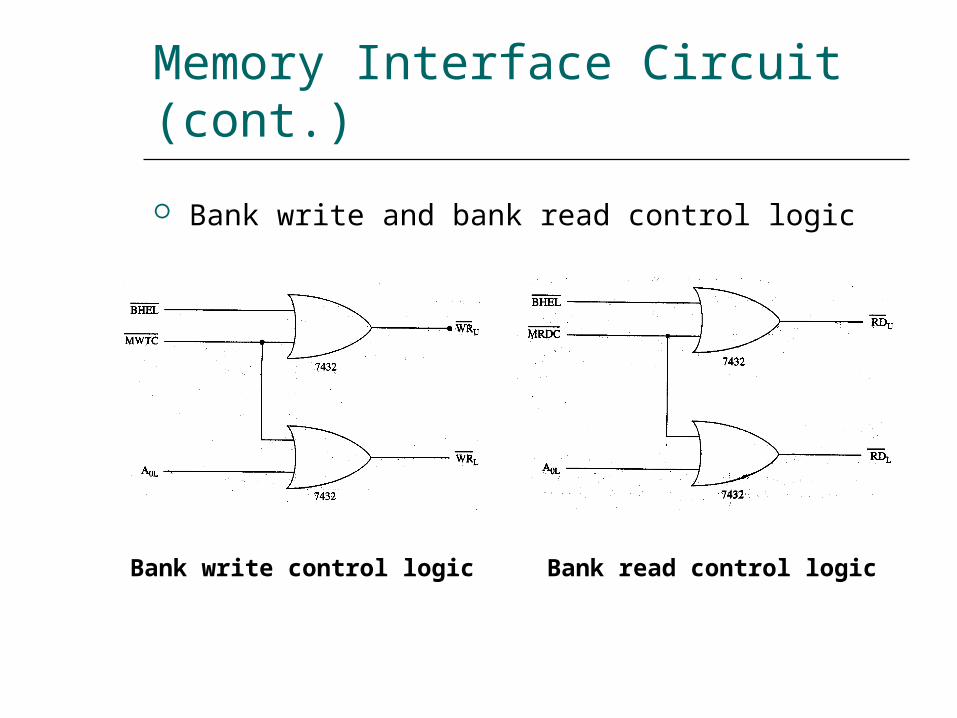
Memory Interface Circuit (cont)
Address decoder
Circuit diagram of the 74F139 decoder
Memory Interface Circuit (cont)
Address decoder
Address decoder circuit using 74F139
Memory Interface Circuit (cont)
Address decoder
Block diagram and operation of the 74F138 decoder
Memory Interface Circuit (cont)
Address decoder
Circuit diagram of the 74F138 decoder
Memory Interface Circuit (cont)
Address decoder
Address decoder circuit using 74F138
Types of InputOutput
The IO system allows peripherals to provide data or receive results of processing the data Using IO ports
The 80888086 MPU can employ two types of IO Isolated IO Memory-mapped IO
They differ in how IO ports are mapped into the address space
Types of InputOutput (cont)
Isolated inputoutput When using isolated IO in a microcomputer
system the IO device are treated separate from memory
The memory address space contains 1 M consecutive byte address in the range 0000016 through FFFFF16
The IO address space contains 64K consecutive byte addresses in the range 000016 through FFFF16
The bytes in two consecutive IO addresses can be accessed as word-wide data
Page 0 000016 00FF16
Certain IO instructions can only perform in this range
Types of InputOutput (cont)
Isolated inputoutput
80888086 memory and IO address spaces
Types of InputOutput (cont)
Isolated inputoutput
Isolated IO ports
Types of InputOutput (cont)
Isolated inputoutput Advantages
The complete 1Mbyte memory address space is available for use with memory
Special instructions have been provided to perform IO operations with maximized performance
The bytes in two consecutive IO addresses can be accessed as word-wide data
Disadvantages All input and output data transfers must take place
between the AL or AX register and IO port
Types of InputOutput (cont)
Memory-mapped inputoutput MPU looks at the IO port as though it is a storage
location in memory Some of the memory address space is dedicated to IO
ports Instructions that affect data in memory are used
instead of the special IO instructions More instructions and addressing modes are available to
perform IO operations IO transfers can take place between IO port and other
internal registers The memory instructions tend to execute slower
than those specifically designed for isolated IO Part of the memory address space is lost
Types of InputOutput(cont)
Memory-mapped inputoutput
Memory mapped IO ports
Isolated InputOutput Interface
IO devices Keyboard Printer Mouse 82C55A etc
Functions of interface circuit Select the IO port Latch output data Sample input data Synchronize data transfer Translate between TTL voltage levels and those
required to operate the IO devices
Isolated InputOutput Interface (cont)
Minimum-mode interface
Minimum-mode 8088 system IO interface
Isolated InputOutput Interface (cont)
Minimum-mode interface
Minimum-mode 8086 system IO interface
Isolated InputOutput Interface (cont)
Maximum-mode interface
Maximum-mode 8088 system IO interface
Isolated InputOutput Interface (cont)
Maximum-mode interface
Maximum-mode 8086 system IO interface
Isolated InputOutput Interface (cont)
Maximum-mode interface
IO bus cycle status codes
InputOutput Data Transfer
Inputoutput data transfers in the 8088 and 8086 microcomputers can be either byte-wide or word-wide
IO addresses are 16 bits in length and are output by the 8088 to the IO interface over bus lines AD0 through AD7 and A8 through A15
In 8088 the word transfers is performed as two consecutive byte-wide data transfer and takes two bus cycle
In 8086 the word transfers can takes either one or two bus cycle
Word-wide IO ports should be aligned at even-address boundaries
InputOutput Data Instructions
InputOutput Data Instructions(cont)
EXAMPLE Write a sequence of instructions that will output
the data FF16 to a byte-wide output port at address AB16 of the IO address space
Solution First the AL register is loaded with FF16 as an
immediate operand in the instruction
MOV AL 0FFH Now the data in AL can be output to the byte-
wide output port with the instruction
OUT 0ABH AL
InputOutput Data Instructions(cont)
EXAMPLE Write a series of instructions that will output FF16 to an
output port located at address B00016 of the IO address space
Solution The DX register must first be loaded with the address
of the output port This is done with the instructionMOV DX 0B000H
Next the data that are to be output must be loaded into AL with the instruction
MOV AL 0FFH Finally the data are output with the instruction
OUT DX AL
InputOutput Data Instructions(cont)
EXAMPLE Data are to be read in from two byte-wide input
ports at addresses AA16 and A916 and then output as a word-wide output port at address B00016 Write a sequence of instructions to perform this inputoutput operation
InputOutput Data Instructions(cont)
Solution First read in the byte at address AA16 into AL and
move it into AHIN AL 0AAHMOV AH AL
Now the other byte can be read into AL by the instructionIN AL 09AH
And to write out the word of dataMOV DX 0B000HOUT DX AX
InputOutput Bus Cycles
Input bus cycle of the 8088
InputOutput Bus Cycles (cont)
Output bus cycle of the 8088
InputOutput Bus Cycles (cont)
Input bus cycle of the 8086
InputOutput Bus Cycles (cont)
Output bus cycle of the 8086
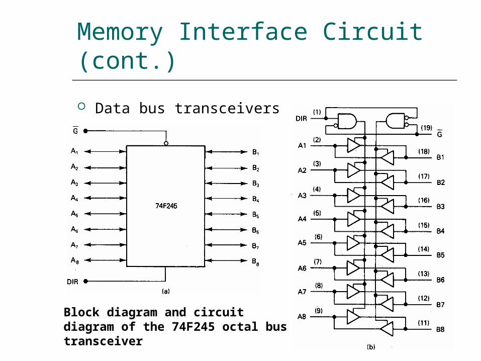
Memory Interface Circuit (cont)
Address decoder
Address decoder circuit using 74F139
Memory Interface Circuit (cont)
Address decoder
Block diagram and operation of the 74F138 decoder
Memory Interface Circuit (cont)
Address decoder
Circuit diagram of the 74F138 decoder
Memory Interface Circuit (cont)
Address decoder
Address decoder circuit using 74F138
Types of InputOutput
The IO system allows peripherals to provide data or receive results of processing the data Using IO ports
The 80888086 MPU can employ two types of IO Isolated IO Memory-mapped IO
They differ in how IO ports are mapped into the address space
Types of InputOutput (cont)
Isolated inputoutput When using isolated IO in a microcomputer
system the IO device are treated separate from memory
The memory address space contains 1 M consecutive byte address in the range 0000016 through FFFFF16
The IO address space contains 64K consecutive byte addresses in the range 000016 through FFFF16
The bytes in two consecutive IO addresses can be accessed as word-wide data
Page 0 000016 00FF16
Certain IO instructions can only perform in this range
Types of InputOutput (cont)
Isolated inputoutput
80888086 memory and IO address spaces
Types of InputOutput (cont)
Isolated inputoutput
Isolated IO ports
Types of InputOutput (cont)
Isolated inputoutput Advantages
The complete 1Mbyte memory address space is available for use with memory
Special instructions have been provided to perform IO operations with maximized performance
The bytes in two consecutive IO addresses can be accessed as word-wide data
Disadvantages All input and output data transfers must take place
between the AL or AX register and IO port
Types of InputOutput (cont)
Memory-mapped inputoutput MPU looks at the IO port as though it is a storage
location in memory Some of the memory address space is dedicated to IO
ports Instructions that affect data in memory are used
instead of the special IO instructions More instructions and addressing modes are available to
perform IO operations IO transfers can take place between IO port and other
internal registers The memory instructions tend to execute slower
than those specifically designed for isolated IO Part of the memory address space is lost
Types of InputOutput(cont)
Memory-mapped inputoutput
Memory mapped IO ports
Isolated InputOutput Interface
IO devices Keyboard Printer Mouse 82C55A etc
Functions of interface circuit Select the IO port Latch output data Sample input data Synchronize data transfer Translate between TTL voltage levels and those
required to operate the IO devices
Isolated InputOutput Interface (cont)
Minimum-mode interface
Minimum-mode 8088 system IO interface
Isolated InputOutput Interface (cont)
Minimum-mode interface
Minimum-mode 8086 system IO interface
Isolated InputOutput Interface (cont)
Maximum-mode interface
Maximum-mode 8088 system IO interface
Isolated InputOutput Interface (cont)
Maximum-mode interface
Maximum-mode 8086 system IO interface
Isolated InputOutput Interface (cont)
Maximum-mode interface
IO bus cycle status codes
InputOutput Data Transfer
Inputoutput data transfers in the 8088 and 8086 microcomputers can be either byte-wide or word-wide
IO addresses are 16 bits in length and are output by the 8088 to the IO interface over bus lines AD0 through AD7 and A8 through A15
In 8088 the word transfers is performed as two consecutive byte-wide data transfer and takes two bus cycle
In 8086 the word transfers can takes either one or two bus cycle
Word-wide IO ports should be aligned at even-address boundaries
InputOutput Data Instructions
InputOutput Data Instructions(cont)
EXAMPLE Write a sequence of instructions that will output
the data FF16 to a byte-wide output port at address AB16 of the IO address space
Solution First the AL register is loaded with FF16 as an
immediate operand in the instruction
MOV AL 0FFH Now the data in AL can be output to the byte-
wide output port with the instruction
OUT 0ABH AL
InputOutput Data Instructions(cont)
EXAMPLE Write a series of instructions that will output FF16 to an
output port located at address B00016 of the IO address space
Solution The DX register must first be loaded with the address
of the output port This is done with the instructionMOV DX 0B000H
Next the data that are to be output must be loaded into AL with the instruction
MOV AL 0FFH Finally the data are output with the instruction
OUT DX AL
InputOutput Data Instructions(cont)
EXAMPLE Data are to be read in from two byte-wide input
ports at addresses AA16 and A916 and then output as a word-wide output port at address B00016 Write a sequence of instructions to perform this inputoutput operation
InputOutput Data Instructions(cont)
Solution First read in the byte at address AA16 into AL and
move it into AHIN AL 0AAHMOV AH AL
Now the other byte can be read into AL by the instructionIN AL 09AH
And to write out the word of dataMOV DX 0B000HOUT DX AX
InputOutput Bus Cycles
Input bus cycle of the 8088
InputOutput Bus Cycles (cont)
Output bus cycle of the 8088
InputOutput Bus Cycles (cont)
Input bus cycle of the 8086
InputOutput Bus Cycles (cont)
Output bus cycle of the 8086
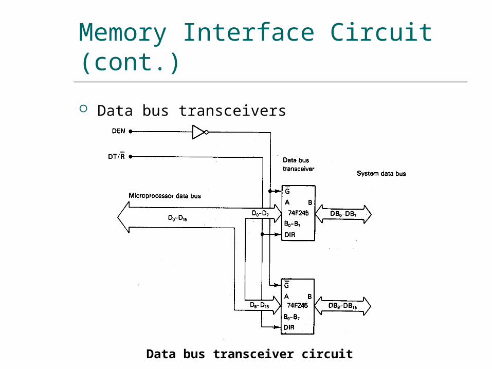
Memory Interface Circuit (cont)
Address decoder
Block diagram and operation of the 74F138 decoder
Memory Interface Circuit (cont)
Address decoder
Circuit diagram of the 74F138 decoder
Memory Interface Circuit (cont)
Address decoder
Address decoder circuit using 74F138
Types of InputOutput
The IO system allows peripherals to provide data or receive results of processing the data Using IO ports
The 80888086 MPU can employ two types of IO Isolated IO Memory-mapped IO
They differ in how IO ports are mapped into the address space
Types of InputOutput (cont)
Isolated inputoutput When using isolated IO in a microcomputer
system the IO device are treated separate from memory
The memory address space contains 1 M consecutive byte address in the range 0000016 through FFFFF16
The IO address space contains 64K consecutive byte addresses in the range 000016 through FFFF16
The bytes in two consecutive IO addresses can be accessed as word-wide data
Page 0 000016 00FF16
Certain IO instructions can only perform in this range
Types of InputOutput (cont)
Isolated inputoutput
80888086 memory and IO address spaces
Types of InputOutput (cont)
Isolated inputoutput
Isolated IO ports
Types of InputOutput (cont)
Isolated inputoutput Advantages
The complete 1Mbyte memory address space is available for use with memory
Special instructions have been provided to perform IO operations with maximized performance
The bytes in two consecutive IO addresses can be accessed as word-wide data
Disadvantages All input and output data transfers must take place
between the AL or AX register and IO port
Types of InputOutput (cont)
Memory-mapped inputoutput MPU looks at the IO port as though it is a storage
location in memory Some of the memory address space is dedicated to IO
ports Instructions that affect data in memory are used
instead of the special IO instructions More instructions and addressing modes are available to
perform IO operations IO transfers can take place between IO port and other
internal registers The memory instructions tend to execute slower
than those specifically designed for isolated IO Part of the memory address space is lost
Types of InputOutput(cont)
Memory-mapped inputoutput
Memory mapped IO ports
Isolated InputOutput Interface
IO devices Keyboard Printer Mouse 82C55A etc
Functions of interface circuit Select the IO port Latch output data Sample input data Synchronize data transfer Translate between TTL voltage levels and those
required to operate the IO devices
Isolated InputOutput Interface (cont)
Minimum-mode interface
Minimum-mode 8088 system IO interface
Isolated InputOutput Interface (cont)
Minimum-mode interface
Minimum-mode 8086 system IO interface
Isolated InputOutput Interface (cont)
Maximum-mode interface
Maximum-mode 8088 system IO interface
Isolated InputOutput Interface (cont)
Maximum-mode interface
Maximum-mode 8086 system IO interface
Isolated InputOutput Interface (cont)
Maximum-mode interface
IO bus cycle status codes
InputOutput Data Transfer
Inputoutput data transfers in the 8088 and 8086 microcomputers can be either byte-wide or word-wide
IO addresses are 16 bits in length and are output by the 8088 to the IO interface over bus lines AD0 through AD7 and A8 through A15
In 8088 the word transfers is performed as two consecutive byte-wide data transfer and takes two bus cycle
In 8086 the word transfers can takes either one or two bus cycle
Word-wide IO ports should be aligned at even-address boundaries
InputOutput Data Instructions
InputOutput Data Instructions(cont)
EXAMPLE Write a sequence of instructions that will output
the data FF16 to a byte-wide output port at address AB16 of the IO address space
Solution First the AL register is loaded with FF16 as an
immediate operand in the instruction
MOV AL 0FFH Now the data in AL can be output to the byte-
wide output port with the instruction
OUT 0ABH AL
InputOutput Data Instructions(cont)
EXAMPLE Write a series of instructions that will output FF16 to an
output port located at address B00016 of the IO address space
Solution The DX register must first be loaded with the address
of the output port This is done with the instructionMOV DX 0B000H
Next the data that are to be output must be loaded into AL with the instruction
MOV AL 0FFH Finally the data are output with the instruction
OUT DX AL
InputOutput Data Instructions(cont)
EXAMPLE Data are to be read in from two byte-wide input
ports at addresses AA16 and A916 and then output as a word-wide output port at address B00016 Write a sequence of instructions to perform this inputoutput operation
InputOutput Data Instructions(cont)
Solution First read in the byte at address AA16 into AL and
move it into AHIN AL 0AAHMOV AH AL
Now the other byte can be read into AL by the instructionIN AL 09AH
And to write out the word of dataMOV DX 0B000HOUT DX AX
InputOutput Bus Cycles
Input bus cycle of the 8088
InputOutput Bus Cycles (cont)
Output bus cycle of the 8088
InputOutput Bus Cycles (cont)
Input bus cycle of the 8086
InputOutput Bus Cycles (cont)
Output bus cycle of the 8086
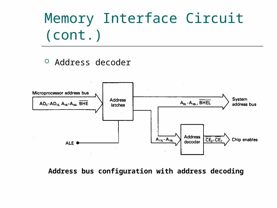
Memory Interface Circuit (cont)
Address decoder
Address decoder circuit using 74F138
Types of InputOutput
The IO system allows peripherals to provide data or receive results of processing the data Using IO ports
The 80888086 MPU can employ two types of IO Isolated IO Memory-mapped IO
They differ in how IO ports are mapped into the address space
Types of InputOutput (cont)
Isolated inputoutput When using isolated IO in a microcomputer
system the IO device are treated separate from memory
The memory address space contains 1 M consecutive byte address in the range 0000016 through FFFFF16
The IO address space contains 64K consecutive byte addresses in the range 000016 through FFFF16
The bytes in two consecutive IO addresses can be accessed as word-wide data
Page 0 000016 00FF16
Certain IO instructions can only perform in this range
Types of InputOutput (cont)
Isolated inputoutput
80888086 memory and IO address spaces
Types of InputOutput (cont)
Isolated inputoutput
Isolated IO ports
Types of InputOutput (cont)
Isolated inputoutput Advantages
The complete 1Mbyte memory address space is available for use with memory
Special instructions have been provided to perform IO operations with maximized performance
The bytes in two consecutive IO addresses can be accessed as word-wide data
Disadvantages All input and output data transfers must take place
between the AL or AX register and IO port
Types of InputOutput (cont)
Memory-mapped inputoutput MPU looks at the IO port as though it is a storage
location in memory Some of the memory address space is dedicated to IO
ports Instructions that affect data in memory are used
instead of the special IO instructions More instructions and addressing modes are available to
perform IO operations IO transfers can take place between IO port and other
internal registers The memory instructions tend to execute slower
than those specifically designed for isolated IO Part of the memory address space is lost
Types of InputOutput(cont)
Memory-mapped inputoutput
Memory mapped IO ports
Isolated InputOutput Interface
IO devices Keyboard Printer Mouse 82C55A etc
Functions of interface circuit Select the IO port Latch output data Sample input data Synchronize data transfer Translate between TTL voltage levels and those
required to operate the IO devices
Isolated InputOutput Interface (cont)
Minimum-mode interface
Minimum-mode 8088 system IO interface
Isolated InputOutput Interface (cont)
Minimum-mode interface
Minimum-mode 8086 system IO interface
Isolated InputOutput Interface (cont)
Maximum-mode interface
Maximum-mode 8088 system IO interface
Isolated InputOutput Interface (cont)
Maximum-mode interface
Maximum-mode 8086 system IO interface
Isolated InputOutput Interface (cont)
Maximum-mode interface
IO bus cycle status codes
InputOutput Data Transfer
Inputoutput data transfers in the 8088 and 8086 microcomputers can be either byte-wide or word-wide
IO addresses are 16 bits in length and are output by the 8088 to the IO interface over bus lines AD0 through AD7 and A8 through A15
In 8088 the word transfers is performed as two consecutive byte-wide data transfer and takes two bus cycle
In 8086 the word transfers can takes either one or two bus cycle
Word-wide IO ports should be aligned at even-address boundaries
InputOutput Data Instructions
InputOutput Data Instructions(cont)
EXAMPLE Write a sequence of instructions that will output
the data FF16 to a byte-wide output port at address AB16 of the IO address space
Solution First the AL register is loaded with FF16 as an
immediate operand in the instruction
MOV AL 0FFH Now the data in AL can be output to the byte-
wide output port with the instruction
OUT 0ABH AL
InputOutput Data Instructions(cont)
EXAMPLE Write a series of instructions that will output FF16 to an
output port located at address B00016 of the IO address space
Solution The DX register must first be loaded with the address
of the output port This is done with the instructionMOV DX 0B000H
Next the data that are to be output must be loaded into AL with the instruction
MOV AL 0FFH Finally the data are output with the instruction
OUT DX AL
InputOutput Data Instructions(cont)
EXAMPLE Data are to be read in from two byte-wide input
ports at addresses AA16 and A916 and then output as a word-wide output port at address B00016 Write a sequence of instructions to perform this inputoutput operation
InputOutput Data Instructions(cont)
Solution First read in the byte at address AA16 into AL and
move it into AHIN AL 0AAHMOV AH AL
Now the other byte can be read into AL by the instructionIN AL 09AH
And to write out the word of dataMOV DX 0B000HOUT DX AX
InputOutput Bus Cycles
Input bus cycle of the 8088
InputOutput Bus Cycles (cont)
Output bus cycle of the 8088
InputOutput Bus Cycles (cont)
Input bus cycle of the 8086
InputOutput Bus Cycles (cont)
Output bus cycle of the 8086
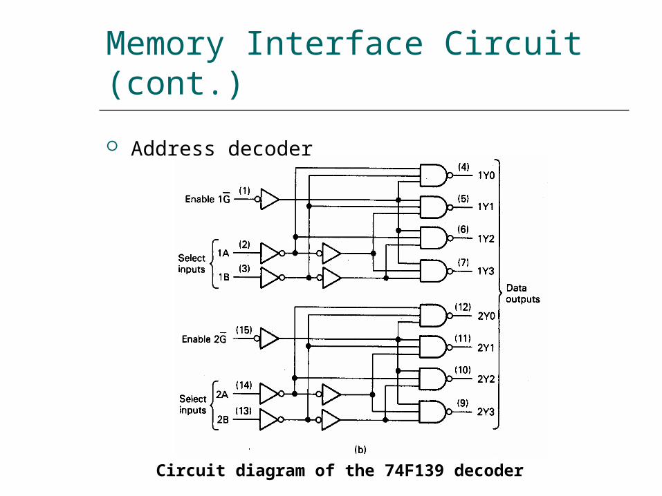
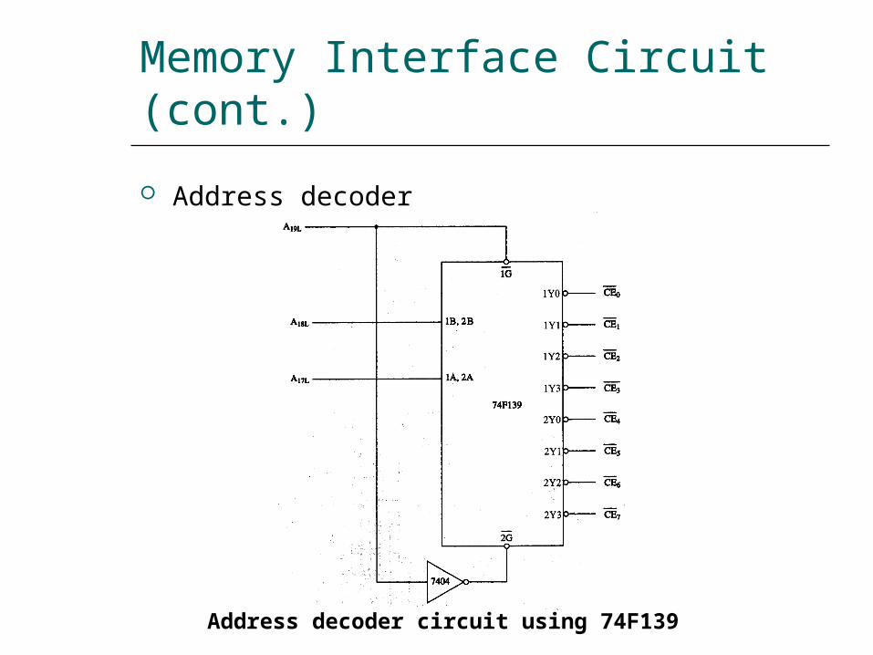
Types of InputOutput (cont)
Isolated inputoutput When using isolated IO in a microcomputer
system the IO device are treated separate from memory
The memory address space contains 1 M consecutive byte address in the range 0000016 through FFFFF16
The IO address space contains 64K consecutive byte addresses in the range 000016 through FFFF16
The bytes in two consecutive IO addresses can be accessed as word-wide data
Page 0 000016 00FF16
Certain IO instructions can only perform in this range
Types of InputOutput (cont)
Isolated inputoutput
80888086 memory and IO address spaces
Types of InputOutput (cont)
Isolated inputoutput
Isolated IO ports
Types of InputOutput (cont)
Isolated inputoutput Advantages
The complete 1Mbyte memory address space is available for use with memory
Special instructions have been provided to perform IO operations with maximized performance
The bytes in two consecutive IO addresses can be accessed as word-wide data
Disadvantages All input and output data transfers must take place
between the AL or AX register and IO port
Types of InputOutput (cont)
Memory-mapped inputoutput MPU looks at the IO port as though it is a storage
location in memory Some of the memory address space is dedicated to IO
ports Instructions that affect data in memory are used
instead of the special IO instructions More instructions and addressing modes are available to
perform IO operations IO transfers can take place between IO port and other
internal registers The memory instructions tend to execute slower
than those specifically designed for isolated IO Part of the memory address space is lost
Types of InputOutput(cont)
Memory-mapped inputoutput
Memory mapped IO ports
Isolated InputOutput Interface
IO devices Keyboard Printer Mouse 82C55A etc
Functions of interface circuit Select the IO port Latch output data Sample input data Synchronize data transfer Translate between TTL voltage levels and those
required to operate the IO devices
Isolated InputOutput Interface (cont)
Minimum-mode interface
Minimum-mode 8088 system IO interface
Isolated InputOutput Interface (cont)
Minimum-mode interface
Minimum-mode 8086 system IO interface
Isolated InputOutput Interface (cont)
Maximum-mode interface
Maximum-mode 8088 system IO interface
Isolated InputOutput Interface (cont)
Maximum-mode interface
Maximum-mode 8086 system IO interface
Isolated InputOutput Interface (cont)
Maximum-mode interface
IO bus cycle status codes
InputOutput Data Transfer
Inputoutput data transfers in the 8088 and 8086 microcomputers can be either byte-wide or word-wide
IO addresses are 16 bits in length and are output by the 8088 to the IO interface over bus lines AD0 through AD7 and A8 through A15
In 8088 the word transfers is performed as two consecutive byte-wide data transfer and takes two bus cycle
In 8086 the word transfers can takes either one or two bus cycle
Word-wide IO ports should be aligned at even-address boundaries
InputOutput Data Instructions
InputOutput Data Instructions(cont)
EXAMPLE Write a sequence of instructions that will output
the data FF16 to a byte-wide output port at address AB16 of the IO address space
Solution First the AL register is loaded with FF16 as an
immediate operand in the instruction
MOV AL 0FFH Now the data in AL can be output to the byte-
wide output port with the instruction
OUT 0ABH AL
InputOutput Data Instructions(cont)
EXAMPLE Write a series of instructions that will output FF16 to an
output port located at address B00016 of the IO address space
Solution The DX register must first be loaded with the address
of the output port This is done with the instructionMOV DX 0B000H
Next the data that are to be output must be loaded into AL with the instruction
MOV AL 0FFH Finally the data are output with the instruction
OUT DX AL
InputOutput Data Instructions(cont)
EXAMPLE Data are to be read in from two byte-wide input
ports at addresses AA16 and A916 and then output as a word-wide output port at address B00016 Write a sequence of instructions to perform this inputoutput operation
InputOutput Data Instructions(cont)
Solution First read in the byte at address AA16 into AL and
move it into AHIN AL 0AAHMOV AH AL
Now the other byte can be read into AL by the instructionIN AL 09AH
And to write out the word of dataMOV DX 0B000HOUT DX AX
InputOutput Bus Cycles
Input bus cycle of the 8088
InputOutput Bus Cycles (cont)
Output bus cycle of the 8088
InputOutput Bus Cycles (cont)
Input bus cycle of the 8086
InputOutput Bus Cycles (cont)
Output bus cycle of the 8086
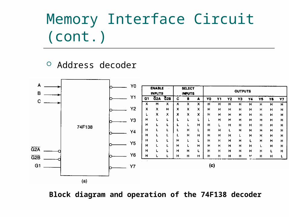
Types of InputOutput (cont)
Isolated inputoutput
80888086 memory and IO address spaces
Types of InputOutput (cont)
Isolated inputoutput
Isolated IO ports
Types of InputOutput (cont)
Isolated inputoutput Advantages
The complete 1Mbyte memory address space is available for use with memory
Special instructions have been provided to perform IO operations with maximized performance
The bytes in two consecutive IO addresses can be accessed as word-wide data
Disadvantages All input and output data transfers must take place
between the AL or AX register and IO port
Types of InputOutput (cont)
Memory-mapped inputoutput MPU looks at the IO port as though it is a storage
location in memory Some of the memory address space is dedicated to IO
ports Instructions that affect data in memory are used
instead of the special IO instructions More instructions and addressing modes are available to
perform IO operations IO transfers can take place between IO port and other
internal registers The memory instructions tend to execute slower
than those specifically designed for isolated IO Part of the memory address space is lost
Types of InputOutput(cont)
Memory-mapped inputoutput
Memory mapped IO ports
Isolated InputOutput Interface
IO devices Keyboard Printer Mouse 82C55A etc
Functions of interface circuit Select the IO port Latch output data Sample input data Synchronize data transfer Translate between TTL voltage levels and those
required to operate the IO devices
Isolated InputOutput Interface (cont)
Minimum-mode interface
Minimum-mode 8088 system IO interface
Isolated InputOutput Interface (cont)
Minimum-mode interface
Minimum-mode 8086 system IO interface
Isolated InputOutput Interface (cont)
Maximum-mode interface
Maximum-mode 8088 system IO interface
Isolated InputOutput Interface (cont)
Maximum-mode interface
Maximum-mode 8086 system IO interface
Isolated InputOutput Interface (cont)
Maximum-mode interface
IO bus cycle status codes
InputOutput Data Transfer
Inputoutput data transfers in the 8088 and 8086 microcomputers can be either byte-wide or word-wide
IO addresses are 16 bits in length and are output by the 8088 to the IO interface over bus lines AD0 through AD7 and A8 through A15
In 8088 the word transfers is performed as two consecutive byte-wide data transfer and takes two bus cycle
In 8086 the word transfers can takes either one or two bus cycle
Word-wide IO ports should be aligned at even-address boundaries
InputOutput Data Instructions
InputOutput Data Instructions(cont)
EXAMPLE Write a sequence of instructions that will output
the data FF16 to a byte-wide output port at address AB16 of the IO address space
Solution First the AL register is loaded with FF16 as an
immediate operand in the instruction
MOV AL 0FFH Now the data in AL can be output to the byte-
wide output port with the instruction
OUT 0ABH AL
InputOutput Data Instructions(cont)
EXAMPLE Write a series of instructions that will output FF16 to an
output port located at address B00016 of the IO address space
Solution The DX register must first be loaded with the address
of the output port This is done with the instructionMOV DX 0B000H
Next the data that are to be output must be loaded into AL with the instruction
MOV AL 0FFH Finally the data are output with the instruction
OUT DX AL
InputOutput Data Instructions(cont)
EXAMPLE Data are to be read in from two byte-wide input
ports at addresses AA16 and A916 and then output as a word-wide output port at address B00016 Write a sequence of instructions to perform this inputoutput operation
InputOutput Data Instructions(cont)
Solution First read in the byte at address AA16 into AL and
move it into AHIN AL 0AAHMOV AH AL
Now the other byte can be read into AL by the instructionIN AL 09AH
And to write out the word of dataMOV DX 0B000HOUT DX AX
InputOutput Bus Cycles
Input bus cycle of the 8088
InputOutput Bus Cycles (cont)
Output bus cycle of the 8088
InputOutput Bus Cycles (cont)
Input bus cycle of the 8086
InputOutput Bus Cycles (cont)
Output bus cycle of the 8086
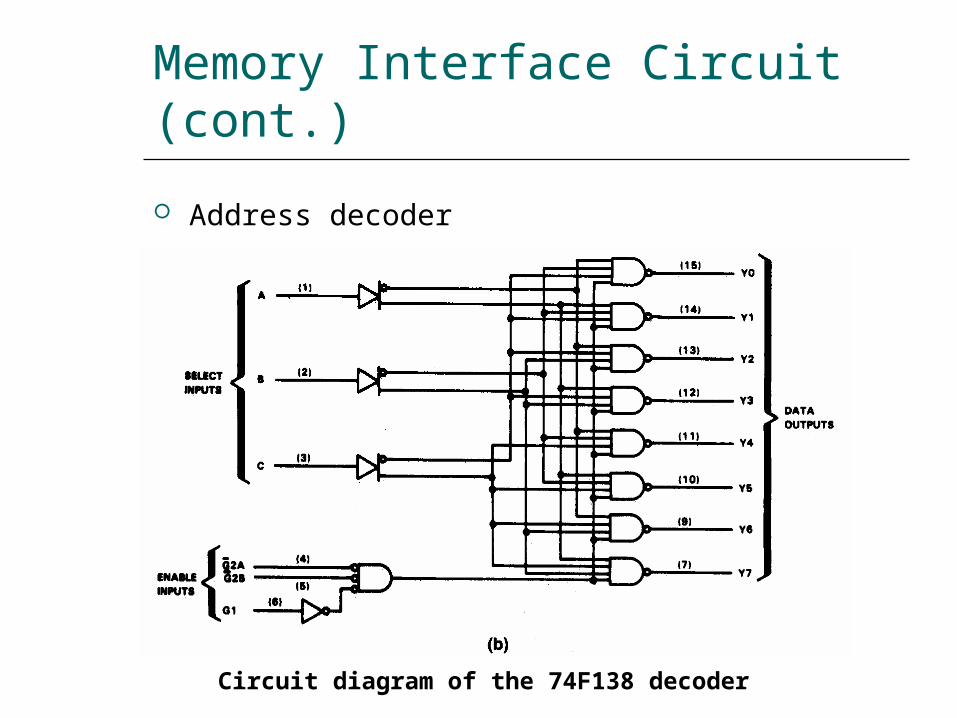
Types of InputOutput (cont)
Isolated inputoutput
Isolated IO ports
Types of InputOutput (cont)
Isolated inputoutput Advantages
The complete 1Mbyte memory address space is available for use with memory
Special instructions have been provided to perform IO operations with maximized performance
The bytes in two consecutive IO addresses can be accessed as word-wide data
Disadvantages All input and output data transfers must take place
between the AL or AX register and IO port
Types of InputOutput (cont)
Memory-mapped inputoutput MPU looks at the IO port as though it is a storage
location in memory Some of the memory address space is dedicated to IO
ports Instructions that affect data in memory are used
instead of the special IO instructions More instructions and addressing modes are available to
perform IO operations IO transfers can take place between IO port and other
internal registers The memory instructions tend to execute slower
than those specifically designed for isolated IO Part of the memory address space is lost
Types of InputOutput(cont)
Memory-mapped inputoutput
Memory mapped IO ports
Isolated InputOutput Interface
IO devices Keyboard Printer Mouse 82C55A etc
Functions of interface circuit Select the IO port Latch output data Sample input data Synchronize data transfer Translate between TTL voltage levels and those
required to operate the IO devices
Isolated InputOutput Interface (cont)
Minimum-mode interface
Minimum-mode 8088 system IO interface
Isolated InputOutput Interface (cont)
Minimum-mode interface
Minimum-mode 8086 system IO interface
Isolated InputOutput Interface (cont)
Maximum-mode interface
Maximum-mode 8088 system IO interface
Isolated InputOutput Interface (cont)
Maximum-mode interface
Maximum-mode 8086 system IO interface
Isolated InputOutput Interface (cont)
Maximum-mode interface
IO bus cycle status codes
InputOutput Data Transfer
Inputoutput data transfers in the 8088 and 8086 microcomputers can be either byte-wide or word-wide
IO addresses are 16 bits in length and are output by the 8088 to the IO interface over bus lines AD0 through AD7 and A8 through A15
In 8088 the word transfers is performed as two consecutive byte-wide data transfer and takes two bus cycle
In 8086 the word transfers can takes either one or two bus cycle
Word-wide IO ports should be aligned at even-address boundaries
InputOutput Data Instructions
InputOutput Data Instructions(cont)
EXAMPLE Write a sequence of instructions that will output
the data FF16 to a byte-wide output port at address AB16 of the IO address space
Solution First the AL register is loaded with FF16 as an
immediate operand in the instruction
MOV AL 0FFH Now the data in AL can be output to the byte-
wide output port with the instruction
OUT 0ABH AL
InputOutput Data Instructions(cont)
EXAMPLE Write a series of instructions that will output FF16 to an
output port located at address B00016 of the IO address space
Solution The DX register must first be loaded with the address
of the output port This is done with the instructionMOV DX 0B000H
Next the data that are to be output must be loaded into AL with the instruction
MOV AL 0FFH Finally the data are output with the instruction
OUT DX AL
InputOutput Data Instructions(cont)
EXAMPLE Data are to be read in from two byte-wide input
ports at addresses AA16 and A916 and then output as a word-wide output port at address B00016 Write a sequence of instructions to perform this inputoutput operation
InputOutput Data Instructions(cont)
Solution First read in the byte at address AA16 into AL and
move it into AHIN AL 0AAHMOV AH AL
Now the other byte can be read into AL by the instructionIN AL 09AH
And to write out the word of dataMOV DX 0B000HOUT DX AX
InputOutput Bus Cycles
Input bus cycle of the 8088
InputOutput Bus Cycles (cont)
Output bus cycle of the 8088
InputOutput Bus Cycles (cont)
Input bus cycle of the 8086
InputOutput Bus Cycles (cont)
Output bus cycle of the 8086
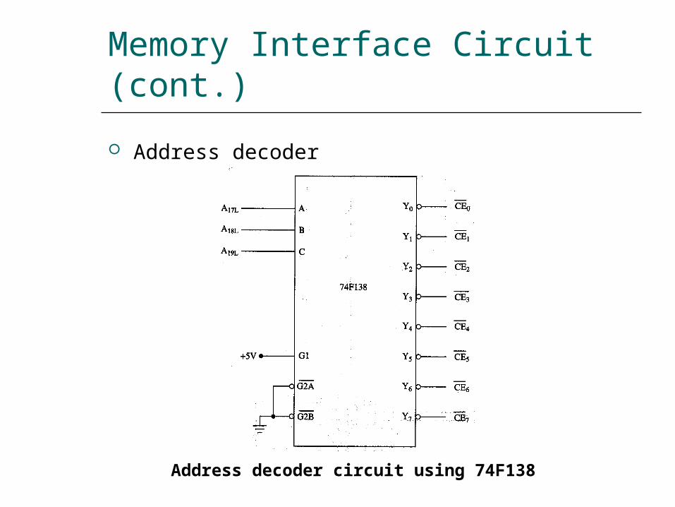
Types of InputOutput (cont)
Isolated inputoutput Advantages
The complete 1Mbyte memory address space is available for use with memory
Special instructions have been provided to perform IO operations with maximized performance
The bytes in two consecutive IO addresses can be accessed as word-wide data
Disadvantages All input and output data transfers must take place
between the AL or AX register and IO port
Types of InputOutput (cont)
Memory-mapped inputoutput MPU looks at the IO port as though it is a storage
location in memory Some of the memory address space is dedicated to IO
ports Instructions that affect data in memory are used
instead of the special IO instructions More instructions and addressing modes are available to
perform IO operations IO transfers can take place between IO port and other
internal registers The memory instructions tend to execute slower
than those specifically designed for isolated IO Part of the memory address space is lost
Types of InputOutput(cont)
Memory-mapped inputoutput
Memory mapped IO ports
Isolated InputOutput Interface
IO devices Keyboard Printer Mouse 82C55A etc
Functions of interface circuit Select the IO port Latch output data Sample input data Synchronize data transfer Translate between TTL voltage levels and those
required to operate the IO devices
Isolated InputOutput Interface (cont)
Minimum-mode interface
Minimum-mode 8088 system IO interface
Isolated InputOutput Interface (cont)
Minimum-mode interface
Minimum-mode 8086 system IO interface
Isolated InputOutput Interface (cont)
Maximum-mode interface
Maximum-mode 8088 system IO interface
Isolated InputOutput Interface (cont)
Maximum-mode interface
Maximum-mode 8086 system IO interface
Isolated InputOutput Interface (cont)
Maximum-mode interface
IO bus cycle status codes
InputOutput Data Transfer
Inputoutput data transfers in the 8088 and 8086 microcomputers can be either byte-wide or word-wide
IO addresses are 16 bits in length and are output by the 8088 to the IO interface over bus lines AD0 through AD7 and A8 through A15
In 8088 the word transfers is performed as two consecutive byte-wide data transfer and takes two bus cycle
In 8086 the word transfers can takes either one or two bus cycle
Word-wide IO ports should be aligned at even-address boundaries
InputOutput Data Instructions
InputOutput Data Instructions(cont)
EXAMPLE Write a sequence of instructions that will output
the data FF16 to a byte-wide output port at address AB16 of the IO address space
Solution First the AL register is loaded with FF16 as an
immediate operand in the instruction
MOV AL 0FFH Now the data in AL can be output to the byte-
wide output port with the instruction
OUT 0ABH AL
InputOutput Data Instructions(cont)
EXAMPLE Write a series of instructions that will output FF16 to an
output port located at address B00016 of the IO address space
Solution The DX register must first be loaded with the address
of the output port This is done with the instructionMOV DX 0B000H
Next the data that are to be output must be loaded into AL with the instruction
MOV AL 0FFH Finally the data are output with the instruction
OUT DX AL
InputOutput Data Instructions(cont)
EXAMPLE Data are to be read in from two byte-wide input
ports at addresses AA16 and A916 and then output as a word-wide output port at address B00016 Write a sequence of instructions to perform this inputoutput operation
InputOutput Data Instructions(cont)
Solution First read in the byte at address AA16 into AL and
move it into AHIN AL 0AAHMOV AH AL
Now the other byte can be read into AL by the instructionIN AL 09AH
And to write out the word of dataMOV DX 0B000HOUT DX AX
InputOutput Bus Cycles
Input bus cycle of the 8088
InputOutput Bus Cycles (cont)
Output bus cycle of the 8088
InputOutput Bus Cycles (cont)
Input bus cycle of the 8086
InputOutput Bus Cycles (cont)
Output bus cycle of the 8086
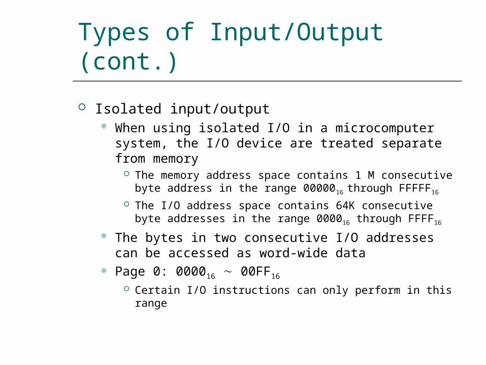
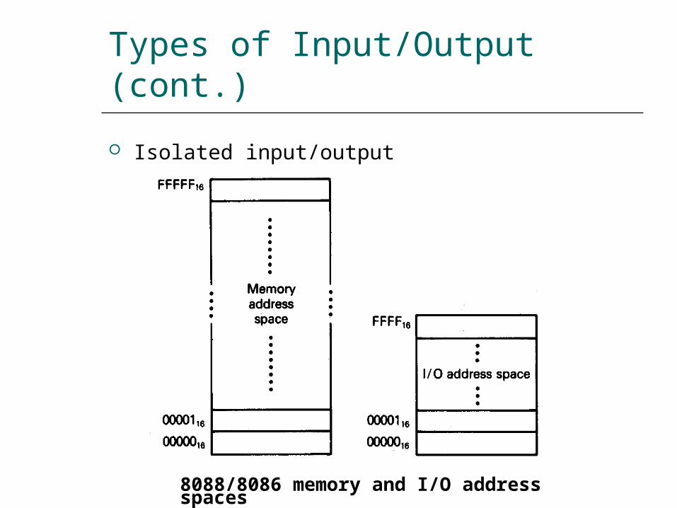

Isolated InputOutput Interface (cont)
Minimum-mode interface
Minimum-mode 8088 system IO interface
Isolated InputOutput Interface (cont)
Minimum-mode interface
Minimum-mode 8086 system IO interface
Isolated InputOutput Interface (cont)
Maximum-mode interface
Maximum-mode 8088 system IO interface
Isolated InputOutput Interface (cont)
Maximum-mode interface
Maximum-mode 8086 system IO interface
Isolated InputOutput Interface (cont)
Maximum-mode interface
IO bus cycle status codes
InputOutput Data Transfer
Inputoutput data transfers in the 8088 and 8086 microcomputers can be either byte-wide or word-wide
IO addresses are 16 bits in length and are output by the 8088 to the IO interface over bus lines AD0 through AD7 and A8 through A15
In 8088 the word transfers is performed as two consecutive byte-wide data transfer and takes two bus cycle
In 8086 the word transfers can takes either one or two bus cycle
Word-wide IO ports should be aligned at even-address boundaries
InputOutput Data Instructions
InputOutput Data Instructions(cont)
EXAMPLE Write a sequence of instructions that will output
the data FF16 to a byte-wide output port at address AB16 of the IO address space
Solution First the AL register is loaded with FF16 as an
immediate operand in the instruction
MOV AL 0FFH Now the data in AL can be output to the byte-
wide output port with the instruction
OUT 0ABH AL
InputOutput Data Instructions(cont)
EXAMPLE Write a series of instructions that will output FF16 to an
output port located at address B00016 of the IO address space
Solution The DX register must first be loaded with the address
of the output port This is done with the instructionMOV DX 0B000H
Next the data that are to be output must be loaded into AL with the instruction
MOV AL 0FFH Finally the data are output with the instruction
OUT DX AL
InputOutput Data Instructions(cont)
EXAMPLE Data are to be read in from two byte-wide input
ports at addresses AA16 and A916 and then output as a word-wide output port at address B00016 Write a sequence of instructions to perform this inputoutput operation
InputOutput Data Instructions(cont)
Solution First read in the byte at address AA16 into AL and
move it into AHIN AL 0AAHMOV AH AL
Now the other byte can be read into AL by the instructionIN AL 09AH
And to write out the word of dataMOV DX 0B000HOUT DX AX
InputOutput Bus Cycles
Input bus cycle of the 8088
InputOutput Bus Cycles (cont)
Output bus cycle of the 8088
InputOutput Bus Cycles (cont)
Input bus cycle of the 8086
InputOutput Bus Cycles (cont)
Output bus cycle of the 8086
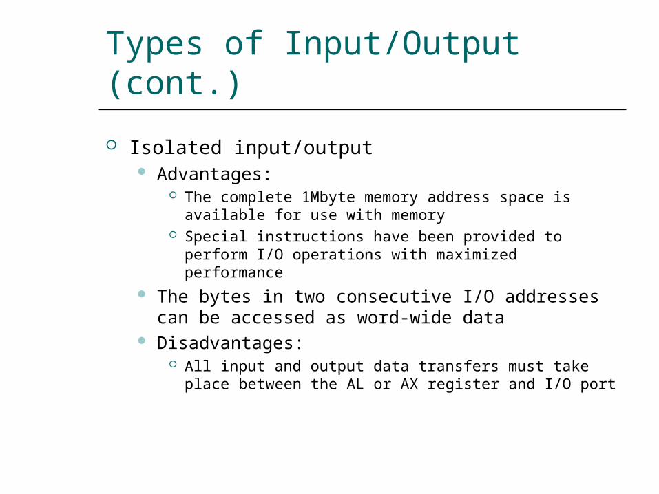
Isolated InputOutput Interface (cont)
Minimum-mode interface
Minimum-mode 8086 system IO interface
Isolated InputOutput Interface (cont)
Maximum-mode interface
Maximum-mode 8088 system IO interface
Isolated InputOutput Interface (cont)
Maximum-mode interface
Maximum-mode 8086 system IO interface
Isolated InputOutput Interface (cont)
Maximum-mode interface
IO bus cycle status codes
InputOutput Data Transfer
Inputoutput data transfers in the 8088 and 8086 microcomputers can be either byte-wide or word-wide
IO addresses are 16 bits in length and are output by the 8088 to the IO interface over bus lines AD0 through AD7 and A8 through A15
In 8088 the word transfers is performed as two consecutive byte-wide data transfer and takes two bus cycle
In 8086 the word transfers can takes either one or two bus cycle
Word-wide IO ports should be aligned at even-address boundaries
InputOutput Data Instructions
InputOutput Data Instructions(cont)
EXAMPLE Write a sequence of instructions that will output
the data FF16 to a byte-wide output port at address AB16 of the IO address space
Solution First the AL register is loaded with FF16 as an
immediate operand in the instruction
MOV AL 0FFH Now the data in AL can be output to the byte-
wide output port with the instruction
OUT 0ABH AL
InputOutput Data Instructions(cont)
EXAMPLE Write a series of instructions that will output FF16 to an
output port located at address B00016 of the IO address space
Solution The DX register must first be loaded with the address
of the output port This is done with the instructionMOV DX 0B000H
Next the data that are to be output must be loaded into AL with the instruction
MOV AL 0FFH Finally the data are output with the instruction
OUT DX AL
InputOutput Data Instructions(cont)
EXAMPLE Data are to be read in from two byte-wide input
ports at addresses AA16 and A916 and then output as a word-wide output port at address B00016 Write a sequence of instructions to perform this inputoutput operation
InputOutput Data Instructions(cont)
Solution First read in the byte at address AA16 into AL and
move it into AHIN AL 0AAHMOV AH AL
Now the other byte can be read into AL by the instructionIN AL 09AH
And to write out the word of dataMOV DX 0B000HOUT DX AX
InputOutput Bus Cycles
Input bus cycle of the 8088
InputOutput Bus Cycles (cont)
Output bus cycle of the 8088
InputOutput Bus Cycles (cont)
Input bus cycle of the 8086
InputOutput Bus Cycles (cont)
Output bus cycle of the 8086
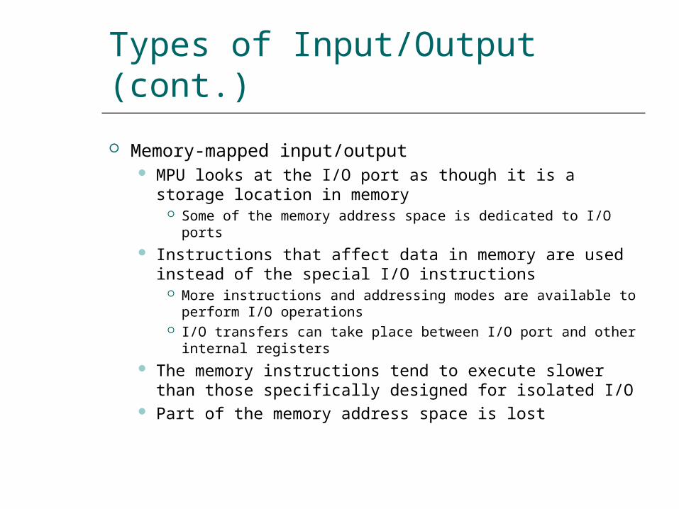
Isolated InputOutput Interface (cont)
Maximum-mode interface
Maximum-mode 8088 system IO interface
Isolated InputOutput Interface (cont)
Maximum-mode interface
Maximum-mode 8086 system IO interface
Isolated InputOutput Interface (cont)
Maximum-mode interface
IO bus cycle status codes
InputOutput Data Transfer
Inputoutput data transfers in the 8088 and 8086 microcomputers can be either byte-wide or word-wide
IO addresses are 16 bits in length and are output by the 8088 to the IO interface over bus lines AD0 through AD7 and A8 through A15
In 8088 the word transfers is performed as two consecutive byte-wide data transfer and takes two bus cycle
In 8086 the word transfers can takes either one or two bus cycle
Word-wide IO ports should be aligned at even-address boundaries
InputOutput Data Instructions
InputOutput Data Instructions(cont)
EXAMPLE Write a sequence of instructions that will output
the data FF16 to a byte-wide output port at address AB16 of the IO address space
Solution First the AL register is loaded with FF16 as an
immediate operand in the instruction
MOV AL 0FFH Now the data in AL can be output to the byte-
wide output port with the instruction
OUT 0ABH AL
InputOutput Data Instructions(cont)
EXAMPLE Write a series of instructions that will output FF16 to an
output port located at address B00016 of the IO address space
Solution The DX register must first be loaded with the address
of the output port This is done with the instructionMOV DX 0B000H
Next the data that are to be output must be loaded into AL with the instruction
MOV AL 0FFH Finally the data are output with the instruction
OUT DX AL
InputOutput Data Instructions(cont)
EXAMPLE Data are to be read in from two byte-wide input
ports at addresses AA16 and A916 and then output as a word-wide output port at address B00016 Write a sequence of instructions to perform this inputoutput operation
InputOutput Data Instructions(cont)
Solution First read in the byte at address AA16 into AL and
move it into AHIN AL 0AAHMOV AH AL
Now the other byte can be read into AL by the instructionIN AL 09AH
And to write out the word of dataMOV DX 0B000HOUT DX AX
InputOutput Bus Cycles
Input bus cycle of the 8088
InputOutput Bus Cycles (cont)
Output bus cycle of the 8088
InputOutput Bus Cycles (cont)
Input bus cycle of the 8086
InputOutput Bus Cycles (cont)
Output bus cycle of the 8086
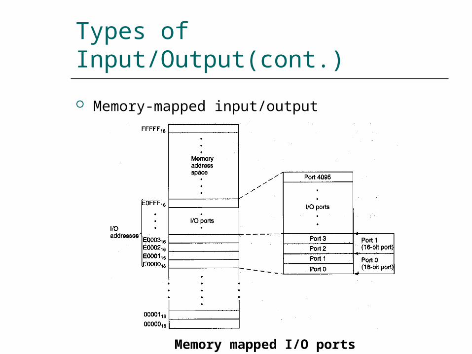
Isolated InputOutput Interface (cont)
Maximum-mode interface
Maximum-mode 8086 system IO interface
Isolated InputOutput Interface (cont)
Maximum-mode interface
IO bus cycle status codes
InputOutput Data Transfer
Inputoutput data transfers in the 8088 and 8086 microcomputers can be either byte-wide or word-wide
IO addresses are 16 bits in length and are output by the 8088 to the IO interface over bus lines AD0 through AD7 and A8 through A15
In 8088 the word transfers is performed as two consecutive byte-wide data transfer and takes two bus cycle
In 8086 the word transfers can takes either one or two bus cycle
Word-wide IO ports should be aligned at even-address boundaries
InputOutput Data Instructions
InputOutput Data Instructions(cont)
EXAMPLE Write a sequence of instructions that will output
the data FF16 to a byte-wide output port at address AB16 of the IO address space
Solution First the AL register is loaded with FF16 as an
immediate operand in the instruction
MOV AL 0FFH Now the data in AL can be output to the byte-
wide output port with the instruction
OUT 0ABH AL
InputOutput Data Instructions(cont)
EXAMPLE Write a series of instructions that will output FF16 to an
output port located at address B00016 of the IO address space
Solution The DX register must first be loaded with the address
of the output port This is done with the instructionMOV DX 0B000H
Next the data that are to be output must be loaded into AL with the instruction
MOV AL 0FFH Finally the data are output with the instruction
OUT DX AL
InputOutput Data Instructions(cont)
EXAMPLE Data are to be read in from two byte-wide input
ports at addresses AA16 and A916 and then output as a word-wide output port at address B00016 Write a sequence of instructions to perform this inputoutput operation
InputOutput Data Instructions(cont)
Solution First read in the byte at address AA16 into AL and
move it into AHIN AL 0AAHMOV AH AL
Now the other byte can be read into AL by the instructionIN AL 09AH
And to write out the word of dataMOV DX 0B000HOUT DX AX
InputOutput Bus Cycles
Input bus cycle of the 8088
InputOutput Bus Cycles (cont)
Output bus cycle of the 8088
InputOutput Bus Cycles (cont)
Input bus cycle of the 8086
InputOutput Bus Cycles (cont)
Output bus cycle of the 8086
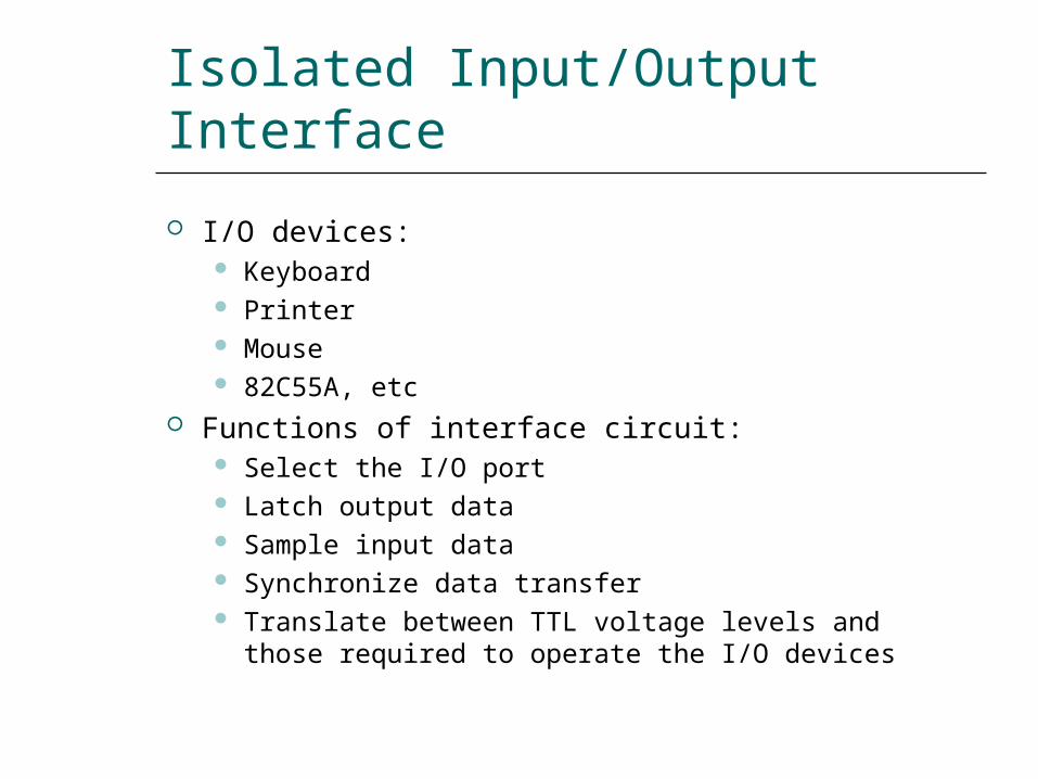
Isolated InputOutput Interface (cont)
Maximum-mode interface
IO bus cycle status codes
InputOutput Data Transfer
Inputoutput data transfers in the 8088 and 8086 microcomputers can be either byte-wide or word-wide
IO addresses are 16 bits in length and are output by the 8088 to the IO interface over bus lines AD0 through AD7 and A8 through A15
In 8088 the word transfers is performed as two consecutive byte-wide data transfer and takes two bus cycle
In 8086 the word transfers can takes either one or two bus cycle
Word-wide IO ports should be aligned at even-address boundaries
InputOutput Data Instructions
InputOutput Data Instructions(cont)
EXAMPLE Write a sequence of instructions that will output
the data FF16 to a byte-wide output port at address AB16 of the IO address space
Solution First the AL register is loaded with FF16 as an
immediate operand in the instruction
MOV AL 0FFH Now the data in AL can be output to the byte-
wide output port with the instruction
OUT 0ABH AL
InputOutput Data Instructions(cont)
EXAMPLE Write a series of instructions that will output FF16 to an
output port located at address B00016 of the IO address space
Solution The DX register must first be loaded with the address
of the output port This is done with the instructionMOV DX 0B000H
Next the data that are to be output must be loaded into AL with the instruction
MOV AL 0FFH Finally the data are output with the instruction
OUT DX AL
InputOutput Data Instructions(cont)
EXAMPLE Data are to be read in from two byte-wide input
ports at addresses AA16 and A916 and then output as a word-wide output port at address B00016 Write a sequence of instructions to perform this inputoutput operation
InputOutput Data Instructions(cont)
Solution First read in the byte at address AA16 into AL and
move it into AHIN AL 0AAHMOV AH AL
Now the other byte can be read into AL by the instructionIN AL 09AH
And to write out the word of dataMOV DX 0B000HOUT DX AX
InputOutput Bus Cycles
Input bus cycle of the 8088
InputOutput Bus Cycles (cont)
Output bus cycle of the 8088
InputOutput Bus Cycles (cont)
Input bus cycle of the 8086
InputOutput Bus Cycles (cont)
Output bus cycle of the 8086
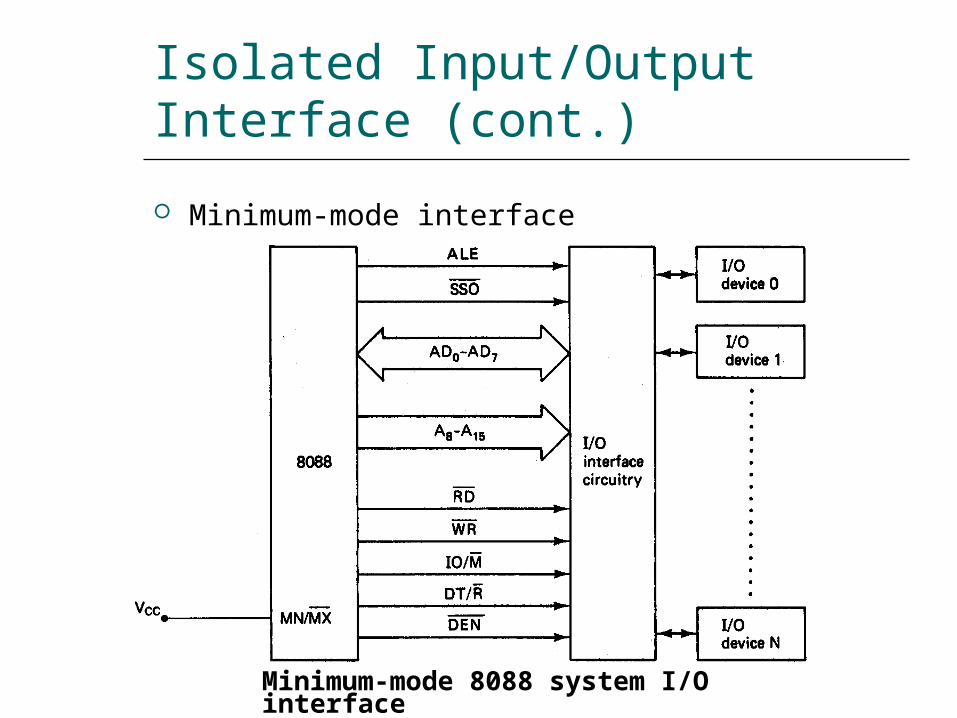
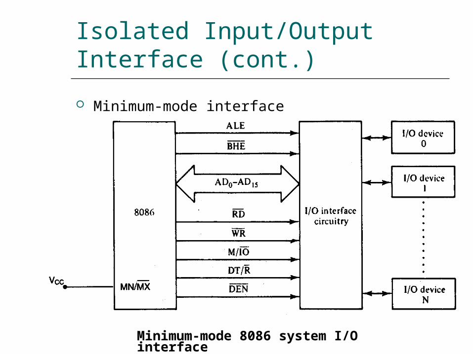
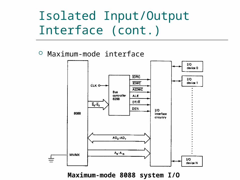
InputOutput Data Instructions(cont)
EXAMPLE Write a sequence of instructions that will output
the data FF16 to a byte-wide output port at address AB16 of the IO address space
Solution First the AL register is loaded with FF16 as an
immediate operand in the instruction
MOV AL 0FFH Now the data in AL can be output to the byte-
wide output port with the instruction
OUT 0ABH AL
InputOutput Data Instructions(cont)
EXAMPLE Write a series of instructions that will output FF16 to an
output port located at address B00016 of the IO address space
Solution The DX register must first be loaded with the address
of the output port This is done with the instructionMOV DX 0B000H
Next the data that are to be output must be loaded into AL with the instruction
MOV AL 0FFH Finally the data are output with the instruction
OUT DX AL
InputOutput Data Instructions(cont)
EXAMPLE Data are to be read in from two byte-wide input
ports at addresses AA16 and A916 and then output as a word-wide output port at address B00016 Write a sequence of instructions to perform this inputoutput operation
InputOutput Data Instructions(cont)
Solution First read in the byte at address AA16 into AL and
move it into AHIN AL 0AAHMOV AH AL
Now the other byte can be read into AL by the instructionIN AL 09AH
And to write out the word of dataMOV DX 0B000HOUT DX AX
InputOutput Bus Cycles
Input bus cycle of the 8088
InputOutput Bus Cycles (cont)
Output bus cycle of the 8088
InputOutput Bus Cycles (cont)
Input bus cycle of the 8086
InputOutput Bus Cycles (cont)
Output bus cycle of the 8086
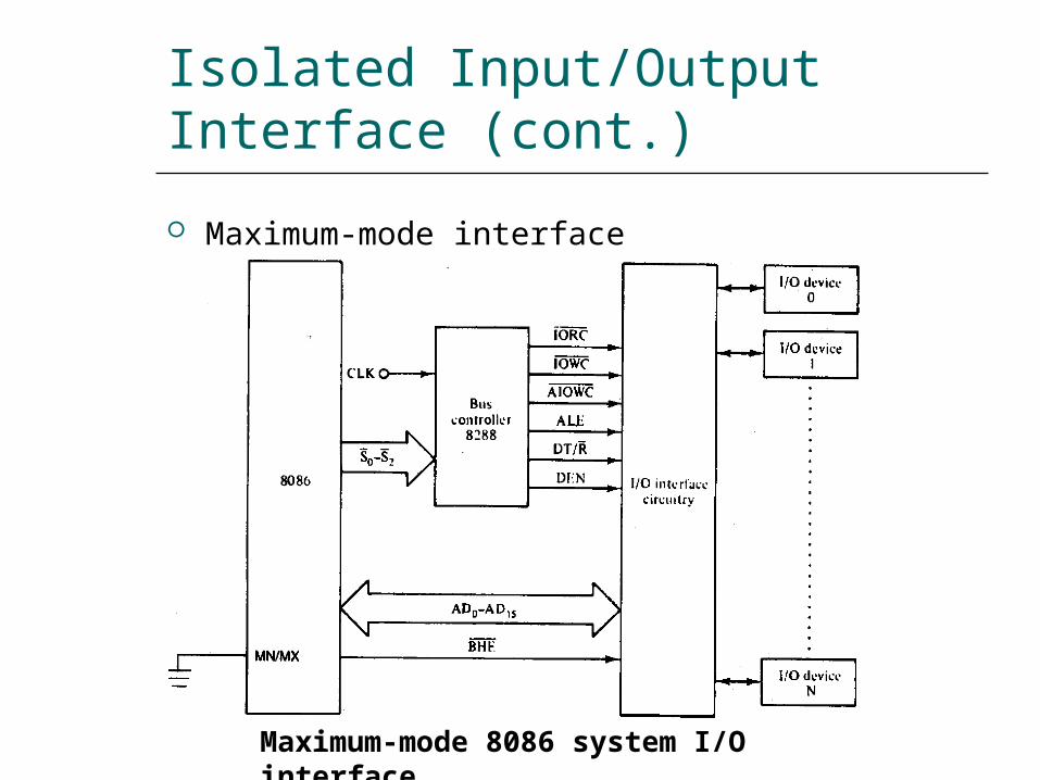
InputOutput Data Instructions(cont)
EXAMPLE Write a series of instructions that will output FF16 to an
output port located at address B00016 of the IO address space
Solution The DX register must first be loaded with the address
of the output port This is done with the instructionMOV DX 0B000H
Next the data that are to be output must be loaded into AL with the instruction
MOV AL 0FFH Finally the data are output with the instruction
OUT DX AL
InputOutput Data Instructions(cont)
EXAMPLE Data are to be read in from two byte-wide input
ports at addresses AA16 and A916 and then output as a word-wide output port at address B00016 Write a sequence of instructions to perform this inputoutput operation
InputOutput Data Instructions(cont)
Solution First read in the byte at address AA16 into AL and
move it into AHIN AL 0AAHMOV AH AL
Now the other byte can be read into AL by the instructionIN AL 09AH
And to write out the word of dataMOV DX 0B000HOUT DX AX
InputOutput Bus Cycles
Input bus cycle of the 8088
InputOutput Bus Cycles (cont)
Output bus cycle of the 8088
InputOutput Bus Cycles (cont)
Input bus cycle of the 8086
InputOutput Bus Cycles (cont)
Output bus cycle of the 8086
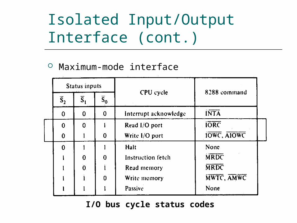
InputOutput Data Instructions(cont)
EXAMPLE Data are to be read in from two byte-wide input
ports at addresses AA16 and A916 and then output as a word-wide output port at address B00016 Write a sequence of instructions to perform this inputoutput operation
InputOutput Data Instructions(cont)
Solution First read in the byte at address AA16 into AL and
move it into AHIN AL 0AAHMOV AH AL
Now the other byte can be read into AL by the instructionIN AL 09AH
And to write out the word of dataMOV DX 0B000HOUT DX AX
InputOutput Bus Cycles
Input bus cycle of the 8088
InputOutput Bus Cycles (cont)
Output bus cycle of the 8088
InputOutput Bus Cycles (cont)
Input bus cycle of the 8086
InputOutput Bus Cycles (cont)
Output bus cycle of the 8086
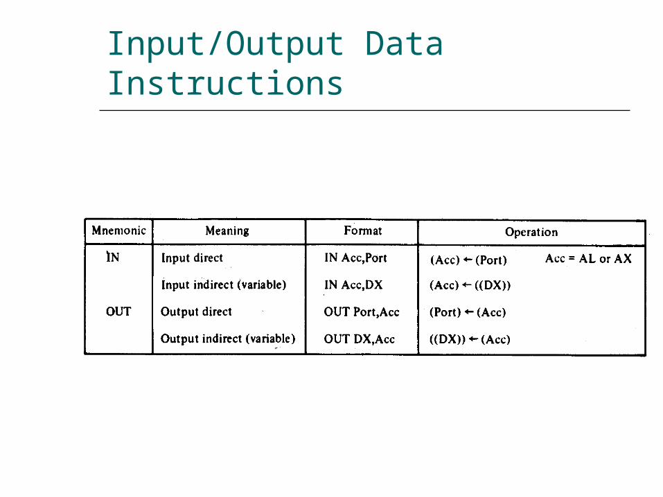
InputOutput Bus Cycles
Input bus cycle of the 8088
InputOutput Bus Cycles (cont)
Output bus cycle of the 8088
InputOutput Bus Cycles (cont)
Input bus cycle of the 8086
InputOutput Bus Cycles (cont)
Output bus cycle of the 8086
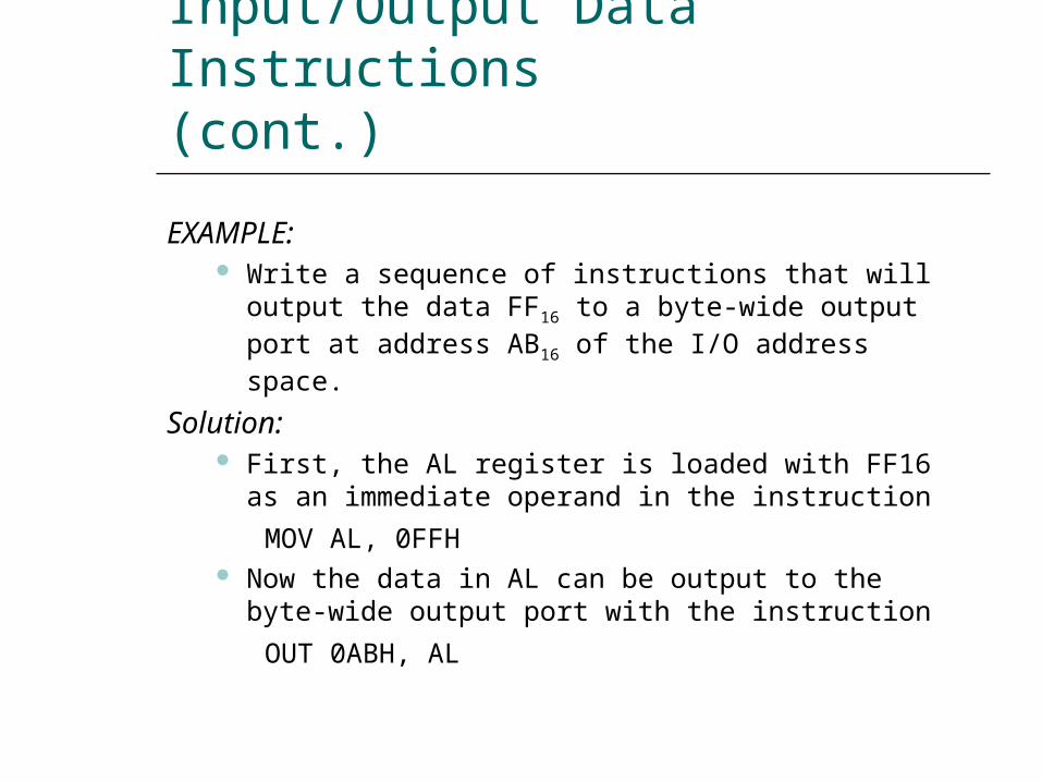
InputOutput Bus Cycles (cont)
Output bus cycle of the 8088
InputOutput Bus Cycles (cont)
Input bus cycle of the 8086
InputOutput Bus Cycles (cont)
Output bus cycle of the 8086
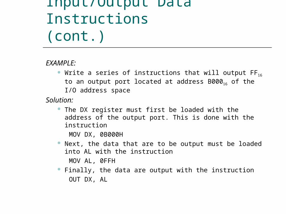
InputOutput Bus Cycles (cont)
Input bus cycle of the 8086
InputOutput Bus Cycles (cont)
Output bus cycle of the 8086
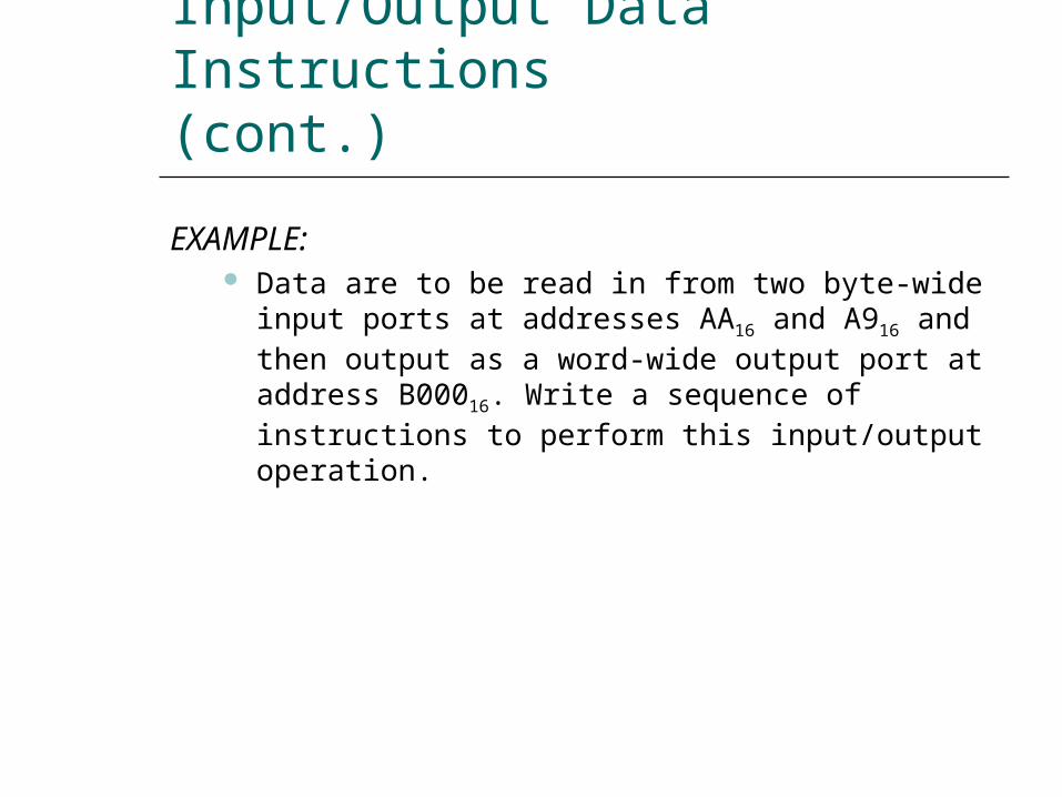
InputOutput Bus Cycles (cont)
Output bus cycle of the 8086