chapter 9 8086/8088 hardware specifications. ch.9 8086/8088 hardware specifications2 introduction...
TRANSCRIPT
Chapter 9
8086/8088 Hardware specifications
Ch.9 8086/8088 Hardware Specifications
2
Introduction
describe pin functions of both 8086 and 8088
provide details :clock generation, bus buffering, bus latching, timing,
wait states, minimum and maximum mode operation
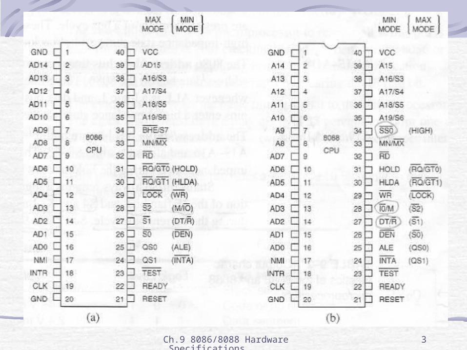
Fig. 9-1 : Pin-outs of 8086/808840-pin dual in-line packages(DIPs)
difference :data bus width → 8086 : 16 bit, 8088 : 8 bit
pin 28 → 8086 : M/IO’, 8088 : IO/M’
pin 34 → 8086 : BHE’/S7, 8088 : SS0
Ch.9 8086/8088 Hardware Specifications
3
Fig. 9-1Fig. 9-1
Ch.9 8086/8088 Hardware Specifications
4
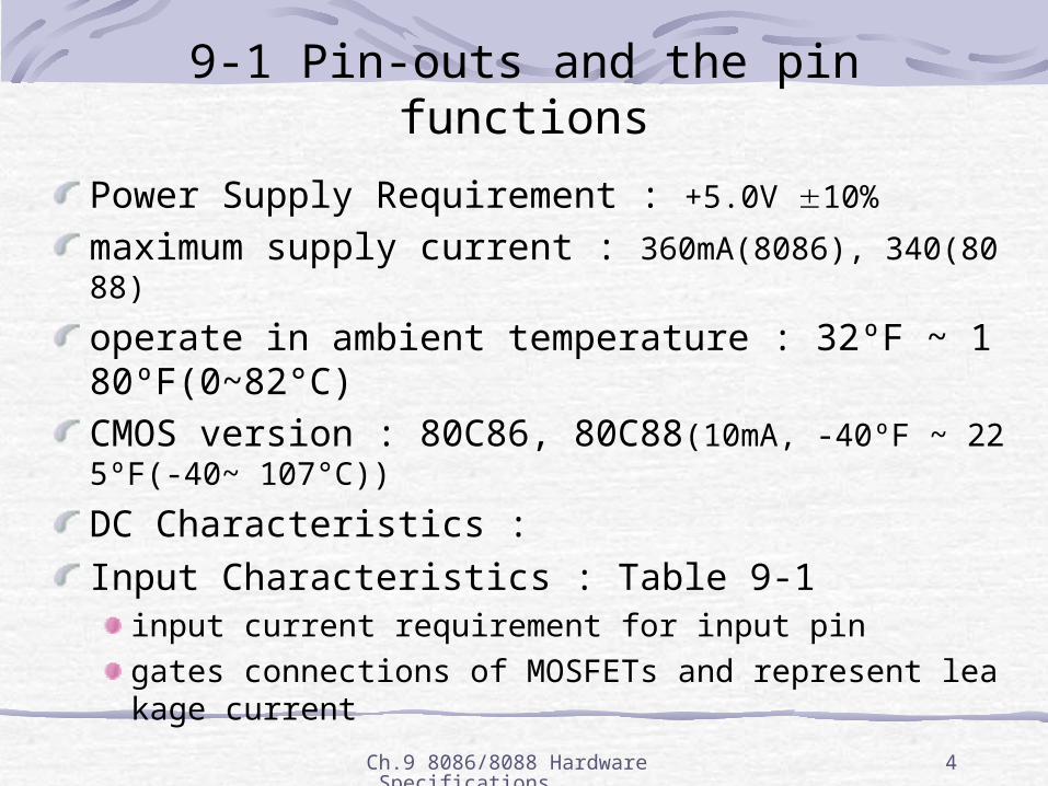
9-1 Pin-outs and the pin functions
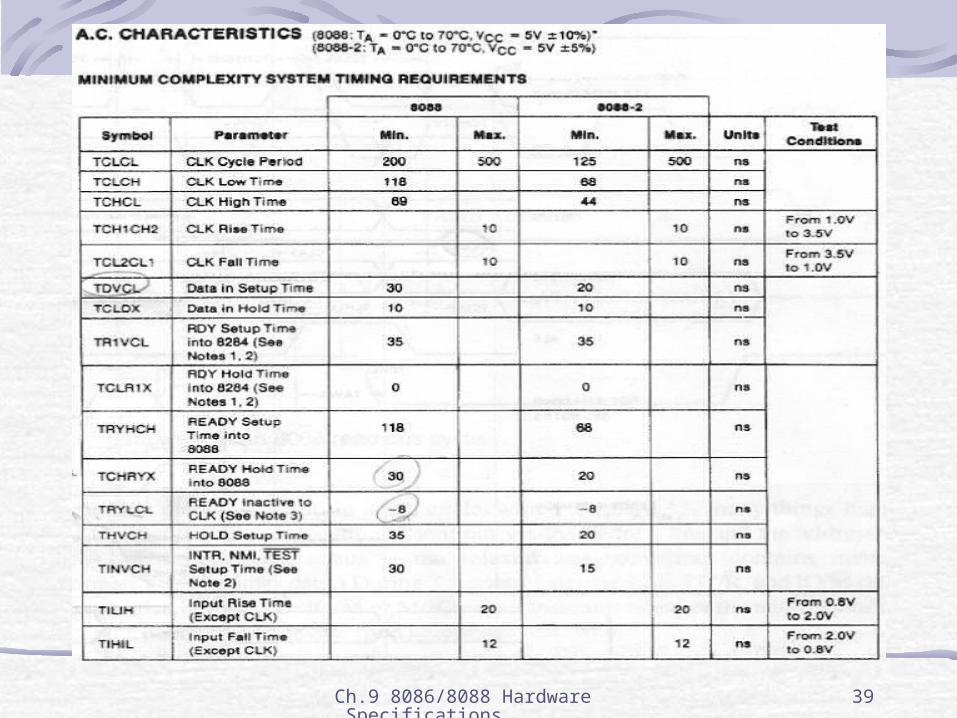
Power Supply Requirement : +5.0V 10%
maximum supply current : 360mA(8086), 340(8088)
operate in ambient temperature : 32ºF ~ 180ºF(0~82°C)
CMOS version : 80C86, 80C88(10mA, -40ºF ~ 225ºF(-40~ 107°C))
DC Characteristics :
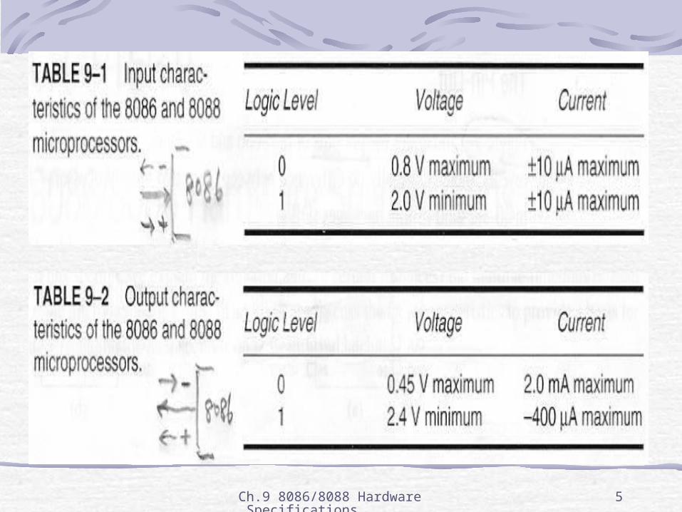
Input Characteristics : Table 9-1input current requirement for input pin
gates connections of MOSFETs and represent leakage current
Ch.9 8086/8088 Hardware Specifications
5
Table 9-1,2Table 9-1,2
Ch.9 8086/8088 Hardware Specifications
6
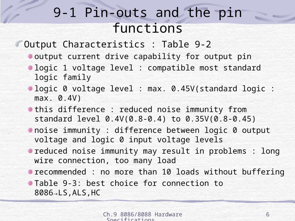
9-1 Pin-outs and the pin functionsOutput Characteristics : Table 9-2
output current drive capability for output pin
logic 1 voltage level : compatible most standard logic family
logic 0 voltage level : max. 0.45V(standard logic : max. 0.4V)
this difference : reduced noise immunity from standard level 0.4V(0.8-0.4) to 0.35V(0.8-0.45)
noise immunity : difference between logic 0 output voltage and logic 0 input voltage levels
reduced noise immunity may result in problems : long wire connection, too many load
recommended : no more than 10 loads without buffering
Table 9-3: best choice for connection to 8086→LS,ALS,HC
Ch.9 8086/8088 Hardware Specifications
7
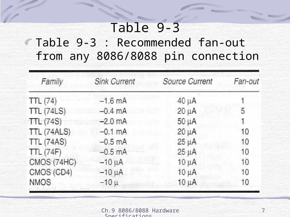
Table 9-3Table 9-3 : Recommended fan-out from any 8086/8088 pin connection
Ch.9 8086/8088 Hardware Specifications
8
Pin Connections
AD7-AD0 : address/data bus(multiplexed)memory address or I/O port no : whenever ALE = 1
data : whenever ALE = 0
high-impedance state : during a hold acknowledge
A15-A8 : 8088 address bushigh-impedance state : during a hold acknowledge
AD15-AD8 : address/data bus(multiplexed)memory address bits A15-A8 : whenever ALE = 1
data bits D15-D8 : whenever ALE = 0
high-impedance state : during a hold acknowledge
Ch.9 8086/8088 Hardware Specifications
9
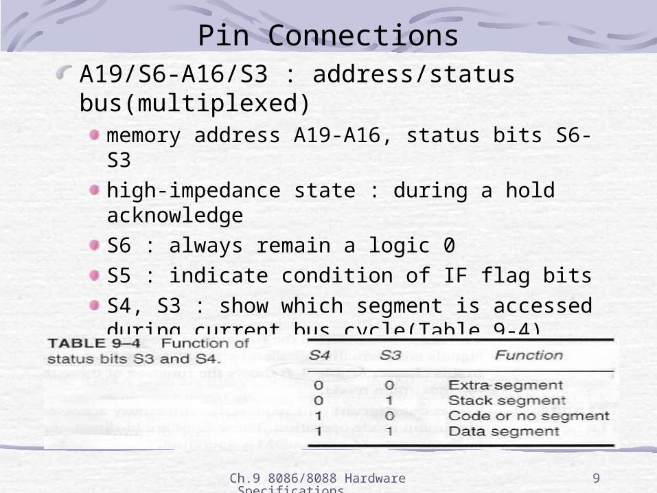
Pin ConnectionsA19/S6-A16/S3 : address/status bus(multiplexed)
memory address A19-A16, status bits S6-S3
high-impedance state : during a hold acknowledge
S6 : always remain a logic 0
S5 : indicate condition of IF flag bits
S4, S3 : show which segment is accessed during current bus cycle(Table 9-4)
S4, S3 : can used to address four separate 1M byte memory banks by decoding them as A21, A20
Ch.9 8086/8088 Hardware Specifications
10
Pin ConnectionsRD’ : read signal
data bus receive data from memory or I/O device :RD’=0
high-impedance state : during a hold acknowledge
READY :µ enter into wait states and remain idle : READY = 0
no effect on the operation of µ : READY = 1
INTR : interrupt requestused to request a hardware interrupt
if INTR is held high when IF = 1 : µ enter interrupt acknowledge cycle(INTA’ become active) after current instruction has complete execution
Ch.9 8086/8088 Hardware Specifications
11
Pin ConnectionsTEST’(BUSY’) : tested by the WAIT instruction
WAIT instruction function as a NOP : if TEST’= 0
WAIT instruction wait for TEST’ to become 0:if TEST’=1
NMI : non-maskable interruptsimilar to INTR except that no check IF flag bit
if NMI is activated : use interrupt vector 2
RESET : µ : reset if RESET held high for a minimum of four clock
CLK(CLOCK) : provide basic timing to µduty cycle of 33%
VCC(power supply) : +5.0V, ±10%
Ch.9 8086/8088 Hardware Specifications
12
Pin ConnectionsGND(Ground) : two pins labeled GND
MN/MX’ : select either minimum or maximum mode
BHE’/S7 : bus high enable
enable the most significant data bus bits(D15-D8) during read or write operation
status of S7 : always a logic 1
Minimum Mode Pins: MN = 1(directly to +5.0V) next p
IO/M’(8088) or M/IO’(8086) : select memory or I/O
address bus : whether memory or I/O port address
WR’ : write signal(high impedance state during hold ack.)
strobe that indicate that output data to memory or I/O
during WR’=0 : data bus contains valid data for M or I/O

Ch.9 8086/8088 Hardware Specifications
13
Fig. 9-1Fig. 9-1
Ch.9 8086/8088 Hardware Specifications
14
Minimum Mode PinsINTA’(interrupt acknowledge) : response to INTR input pin
normally used to gate interrupt vector no onto data bus
ALE(address latch enable) : does not float during hold ack
address/data bus : contain address information
DT/R’(data transmit/receive) :
data bus : transmit(DT/R’=1) or receive(DT/R’=0) data
used to enable external data bus buffers
DEN(data bus enable) : activate external data bus buffers
HOLD : request a direct memory access(DMA)if HOLD=1 : µ stops executing software and places address, data, and control bus at high-impedance state
HOLD=0 : µ execute software normally
Ch.9 8086/8088 Hardware Specifications
15
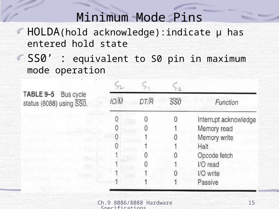
Minimum Mode PinsHOLDA(hold acknowledge):indicate µ has entered hold state
SS0’ : equivalent to S0 pin in maximum mode operation
combined with IO/M’, DT/R’ to decode function of current bus cycle(Table 9-5)
Ch.9 8086/8088 Hardware Specifications
16
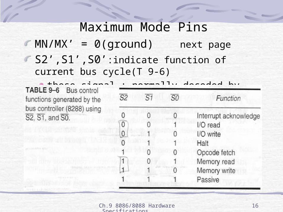
Maximum Mode PinsMN/MX’ = 0(ground) next page
S2’,S1’,S0’:indicate function of current bus cycle(T 9-6)
these signal : normally decoded by 8288 bus controller

Ch.9 8086/8088 Hardware Specifications
17
Fig. 9-1Fig. 9-1
Ch.9 8086/8088 Hardware Specifications
18
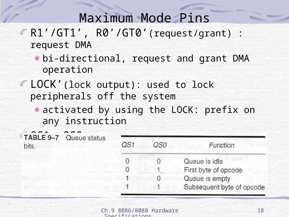
Maximum Mode PinsR1’/GT1’, R0’/GT0’(request/grant) : request DMA
bi-directional, request and grant DMA operation
LOCK’(lock output): used to lock peripherals off the system
activated by using the LOCK: prefix on any instruction
QS1, QS0(queue status) :
show status of internal instruction queue : Table 9-7
provided for access by the numeric coprocessor(8087)
Ch.9 8086/8088 Hardware Specifications
19
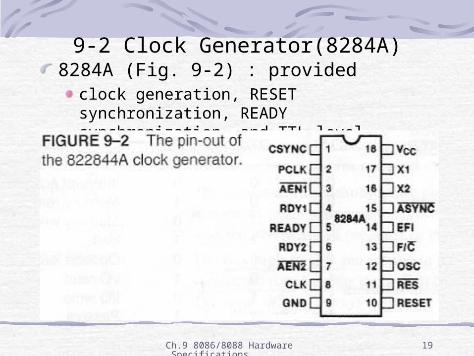
9-2 Clock Generator(8284A)8284A (Fig. 9-2) : provided
clock generation, RESET synchronization, READY synchronization, and TTL-level peripheral clock signal
Ch.9 8086/8088 Hardware Specifications
20
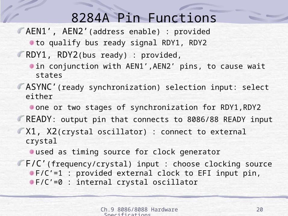
8284A Pin FunctionsAEN1’, AEN2’(address enable) : provided
to qualify bus ready signal RDY1, RDY2
RDY1, RDY2(bus ready) : provided, in conjunction with AEN1’,AEN2’ pins, to cause wait states
ASYNC’(ready synchronization) selection input: select either
one or two stages of synchronization for RDY1,RDY2
READY: output pin that connects to 8086/88 READY input
X1, X2(crystal oscillator) : connect to external crystal
used as timing source for clock generator
F/C’(frequency/crystal) input : choose clocking sourceF/C’=1 : provided external clock to EFI input pin, F/C’=0 : internal crystal oscillator
Ch.9 8086/8088 Hardware Specifications
21
8284A Pin FunctionsEFI(external frequency input) : supplied
the timing whenever F/C’ pin is pulled high
CLK(clock output) : provided CLK input to 8086/8088 and other components1/3 of crystal or EFI input frequency33% duty cycle which is required by 8086/8088
PCLK(peripheral clock) : provided peripheral
1/6 of crystal or EFI input frequency, 50% duty cycle
OSC(oscillator output) : TTL-level signal
same frequency as crystal or EFI input
RES’(reset input) : often connected
to RC network that provide power-on resetting
Ch.9 8086/8088 Hardware Specifications
22
8284A Pin FunctionsRESET output : connected to 8086/8088 RESET input
CSYNC(clock synchronization) : used whenever EFI provides synchronization in system with multiple processors
must be grounded, if internal crystal oscillator is used
GND(ground) : connected to ground
VCC(power supply) : +5.0V ±10%
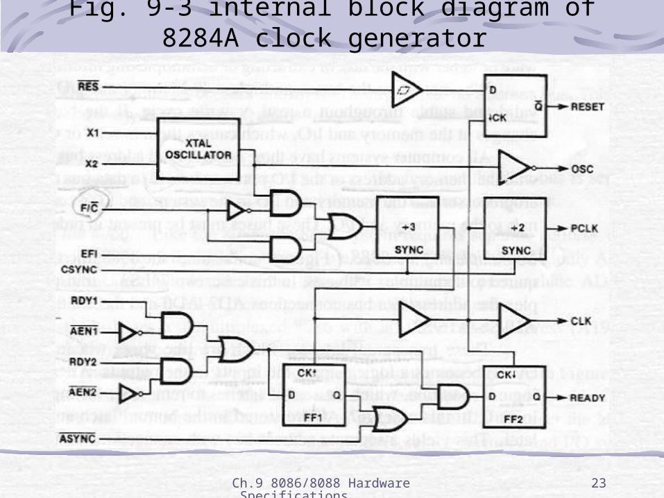
Fig. 9-3 : internal block diagram of 8284Aclock section : middle part
reset section : top part
ready section : bottom part
Ch.9 8086/8088 Hardware Specifications
23
Fig. 9-3 internal block diagram of 8284A clock generator
Fig. 9-3
Ch.9 8086/8088 Hardware Specifications
24
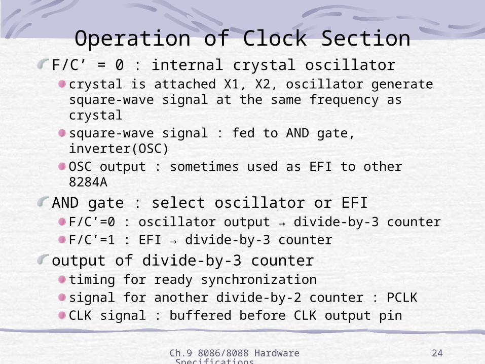
Operation of Clock SectionF/C’ = 0 : internal crystal oscillator
crystal is attached X1, X2, oscillator generate square-wave signal at the same frequency as crystal
square-wave signal : fed to AND gate, inverter(OSC)
OSC output : sometimes used as EFI to other 8284A
AND gate : select oscillator or EFIF/C’=0 : oscillator output → divide-by-3 counter
F/C’=1 : EFI → divide-by-3 counter
output of divide-by-3 countertiming for ready synchronization
signal for another divide-by-2 counter : PCLK
CLK signal : buffered before CLK output pin
Ch.9 8086/8088 Hardware Specifications
25
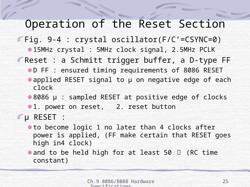
Operation of the Reset Section
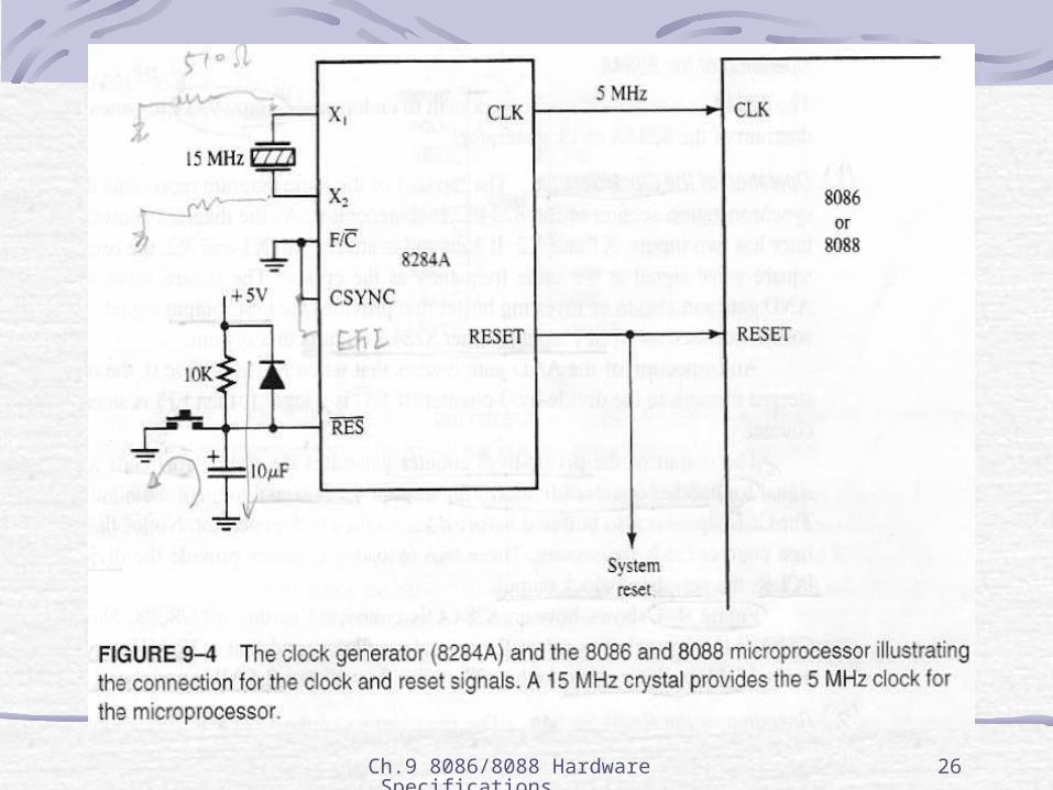
Fig. 9-4 : crystal oscillator(F/C’=CSYNC=0)15MHz crystal : 5MHz clock signal, 2.5MHz PCLK
Reset : a Schmitt trigger buffer, a D-type FFD FF : ensured timing requirements of 8086 RESET
applied RESET signal to µ on negative edge of each clock
8086 µ : sampled RESET at positive edge of clocks
1. power on reset, 2. reset button
µ RESET : to become logic 1 no later than 4 clocks after power is applied, (FF make certain that RESET goes high in4 clock)
and to be held high for at least 50 ㎲ (RC time constant)
Ch.9 8086/8088 Hardware Specifications
26
Fig. 9-4Fig. 9-4
Ch.9 8086/8088 Hardware Specifications
27
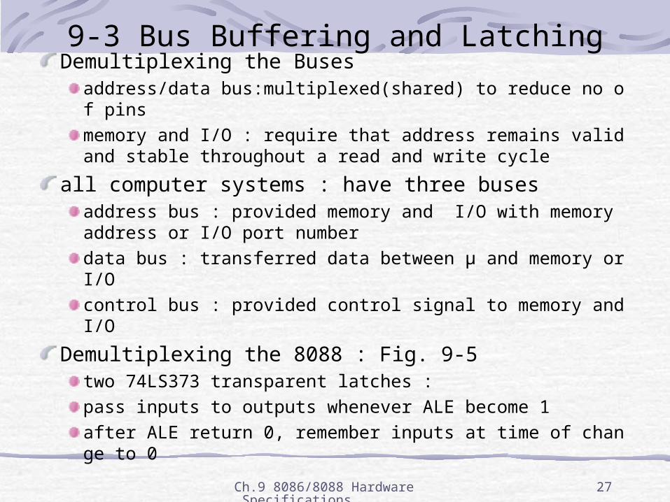
9-3 Bus Buffering and LatchingDemultiplexing the Buses
address/data bus:multiplexed(shared) to reduce no of pins
memory and I/O : require that address remains valid and stable throughout a read and write cycle
all computer systems : have three busesaddress bus : provided memory and I/O with memory address or I/O port number
data bus : transferred data between µ and memory or I/O
control bus : provided control signal to memory and I/O
Demultiplexing the 8088 : Fig. 9-5two 74LS373 transparent latches :
pass inputs to outputs whenever ALE become 1
after ALE return 0, remember inputs at time of change to 0
28
Fig. 9-5Fig. 9-5
Ch.9 8086/8088 Hardware Specifications
29
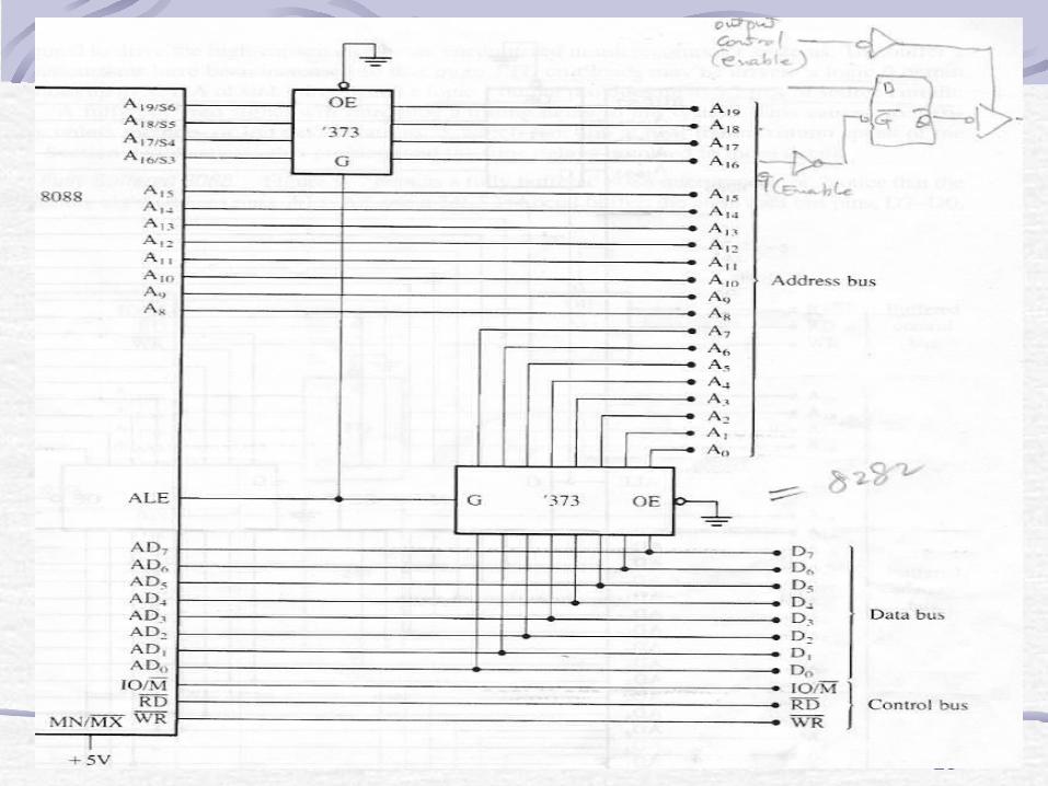
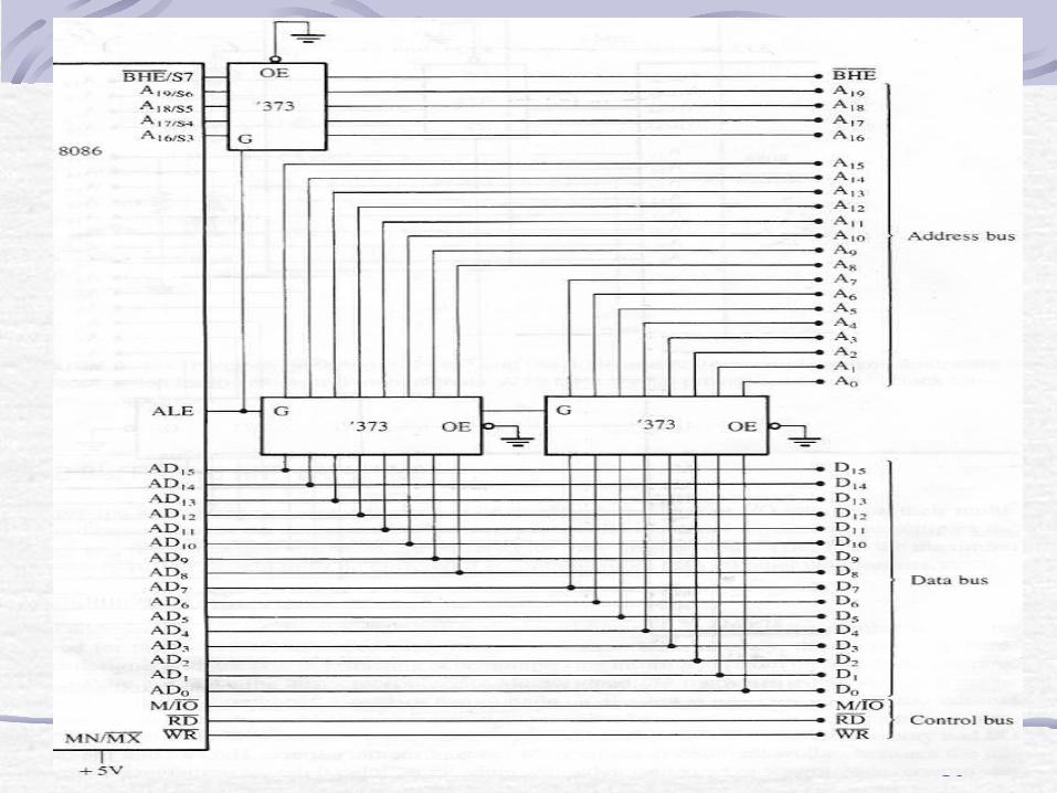
9-3 Bus Buffering and Latching
Demultiplexing the 8086 : Fig. 9-6demultiplexing: AD15-AD0, A19/S6-A16/S3, BHE’/S3
3 buses : address(A19-A0, BHE’), data(D15-D0), control(M/IO’, RD’,WR’)
three 74LS373 transparent latches
The Buffered Systemµ system must be buffered : if more than 10 unit load are attached to any bus pin
demultiplexed pins : already buffered by 74LS373 latch
buffer’s output currents increased : 32mA of sink current(0), 5.2mA of source current(1)
30
Fig. 9-6Fig. 9-6
Ch.9 8086/8088 Hardware Specifications
31
9-3 Bus Buffering and Latching
fully buffered signal : will introduce timing delay
cause no difficulty : unless memory and I/O devices are used, which function at near maximum speed of bus
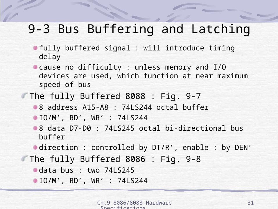
The fully Buffered 8088 : Fig. 9-78 address A15-A8 : 74LS244 octal buffer
IO/M’, RD’, WR’ : 74LS244
8 data D7-D0 : 74LS245 octal bi-directional bus buffer
direction : controlled by DT/R’, enable : by DEN’
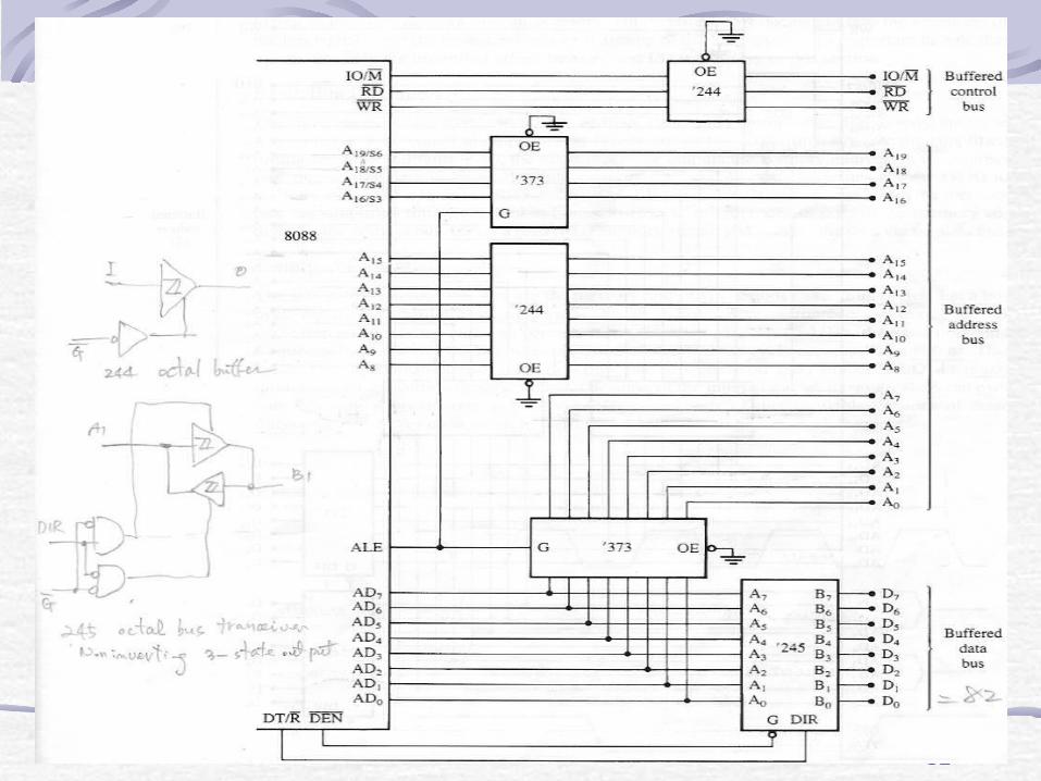
The fully Buffered 8086 : Fig. 9-8data bus : two 74LS245
IO/M’, RD’, WR’ : 74LS244
32
Fig. 9-7Fig. 9-7
33
Fig. 9-8Fig. 9-8
Ch.9 8086/8088 Hardware Specifications
34
9-4 Bus Timing
Basic Bus Operation
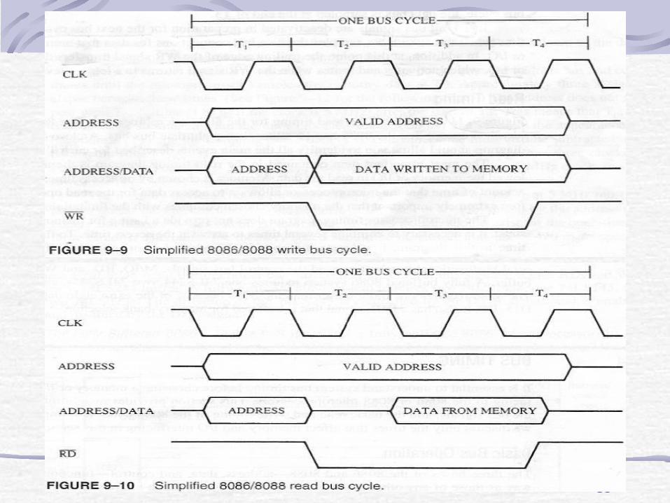
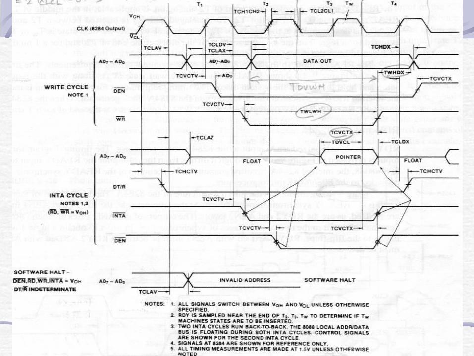
if data are written : Fig. 9-9(address, data, WR’ & M/IO’)
if data are read : Fig. 9-10(address, RD’ & M/IO’)
Timing in General
bus cycle : 8086/8088 µ use memory & I/O in periods called bus cycles
equal 4 (or as few as 2) system-clocking periods(T states)
800ns : 5MHz basic operating frequency
read or write at maximum rate of 1.25 million times a sec.
because internal queue, µ execute 2.5 MIPS in bursts
35
Fig. 9-9,10Fig. 9-9,10
Ch.9 8086/8088 Hardware Specifications
36
Timing in GeneralT1 : 1st clocking period
address of memory or I/O : sent out via address bus
control signal ALE, DT/R’, M/IO’(IO/M’) : output
T2 : issue RD’ or WR’, DEN’
in case of write : data to be written appear on data bus
READY : sampled at the end of T2(Fig. 9-11)if READY is low at end of T2 : T3 becomes a wait state(Tw)
if read bus cycle : data bus is sampled at end of T3
T4 :all bus signals : deactivated in preparation for next bus cycle
µ sampled data bus for data that read from M or I/O
trailing edge of WR’ : transfer data to memory or I/O
Ch.9 8086/8088 Hardware Specifications
37
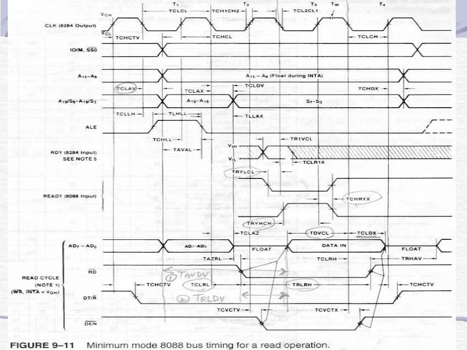
Fig. 9-11Fig. 9-11
Ch.9 8086/8088 Hardware Specifications
38
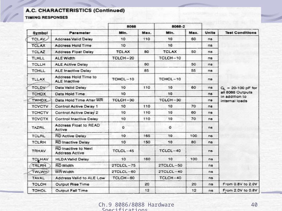
Read TimingFig. 9-11 : depict read timing for 8088/8086
fixed amount of time allowed memory or I/O to read dataat end of T3 : µ sample the data bus
address access time: TAVDV = 3TCLCL - TCLAV - TDVCL = 3200–110–30=460 ns
TCLAV : time that appeared address on address bus
TDVCL : data setup time
time delay(30-40ns) : address decoders and buffersmemory speed : no slower than about 420ns
read access time :TRLDV = 2TCLCL - TCLRL - TDVCL = 2200–165–30=205 ns
width of RD’ strobe :TRLRH = 2TCLCL – 75ns = 2 200 – 75 = 325 ns
Ch.9 8086/8088 Hardware Specifications
39
Fig. 9-12Fig. 9-12
Ch.9 8086/8088 Hardware Specifications
40
Fig. 9-12(continued)Fig. 9-12
Ch.9 8086/8088 Hardware Specifications
41
Write TimingFig. 9-13 : write timing for 8088/8086
main differences : WR’, data bus contain information for memory, DT/R’=1(transmit)
memory data : written at trailing edge of WR’
data hold time :TWHDX = TCLCH – 30ns = 118 – 30 = 88 ns
memory setup time : TDVWH = 2TCLCL–TCLDV+TCVCTX=2200–110+10=300ns
width of WR’ strobe :TWLWH = 2TCLCL – 60ns = 2 200 – 60 = 340 ns
42
Fig. 9-13Fig. 9-13
Ch.9 8086/8088 Hardware Specifications
43
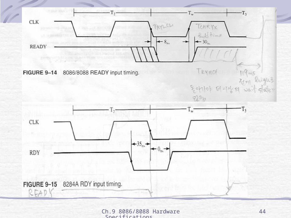
9-5 Ready and the Wait Statewait state(TW) :
an extra clocking period, inserted between T2 & T3
READY input : cause wait states for slower memory & I/O components
sampled at the end of T2, if applicable, in middle of TW
if READY = 0 at end of T2 : T3 is delayed and TW is inserted between T2 and T3
READY is next sampled at middle of TW : to determine whether the next state is TW or T3
timing diagram : Fig. 9-14(Fig. 9-11)required setup and hold time from system clock
met by internal READY synchronization circuit of 8284A
Ch.9 8086/8088 Hardware Specifications
44
Fig. 9-14, 15Fig. 9-14, 15
Ch.9 8086/8088 Hardware Specifications
45
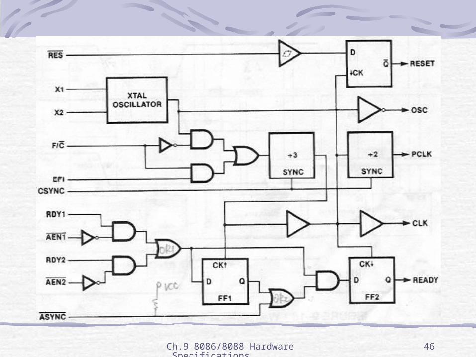
RDY and the 8284ARDY : synchronized ready input to 8284A clock generator
timing diagram : Fig. 9-15
Fig. 9-16 : internal structure of 8284ARDY1•AEN1’ + RDY2•AEN2’ : to generate input to one or two stage of synchronization
ASYNC’=1(open) : select one stage of synchronization
RDY : kept from reaching 8086/88 READY pin until the next negative edge of clock
ASYNC’=0(ground): select two stage of synchronization
on 1st positive edge of clock : 1st FF capture RDY
output of 1st FF : fed to 2nd FF
on next negative edge of clock : 2nd FF capture RDY
Ch.9 8086/8088 Hardware Specifications
46
Fig. 9-16Fig. 9-16
Ch.9 8086/8088 Hardware Specifications
47
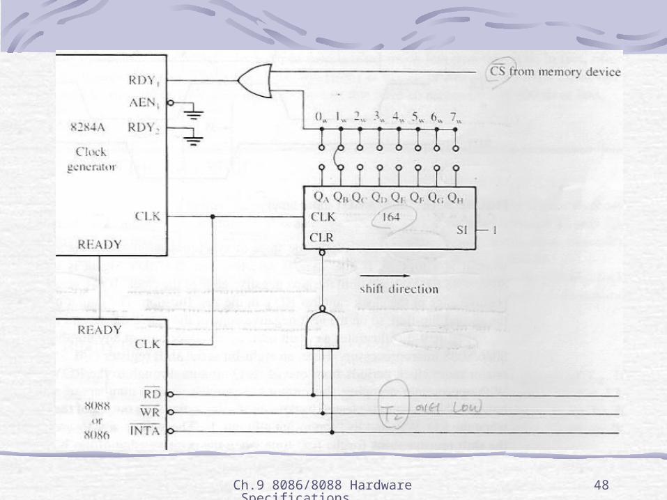
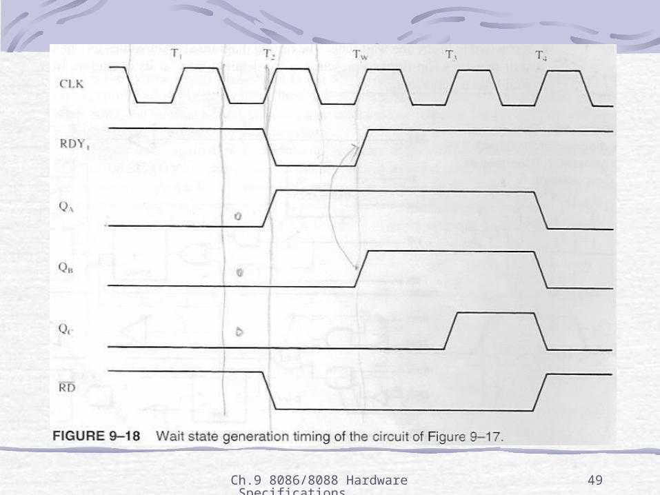
RDY and the 8284AFig. 9-17, 18 :
circuit that generated almost any no of wait states for µ
8-bit shift reg.(74LS164) : shift 0 for one or more clock periods from one of its Q outputs through to RDY1
cleared back to its starting point
RD’=WR’=INTA’=1 : until state T2 → Q = 0
positive edge of T2 : shift right, QA = 1(because SI=1)
RDY1 = 0 : CS’ = 0 or QB = 0
inserted wait cycle
positive edge of TW : shift right, QA = QB = 1
RDY1 = 1 : CS’ = 0 or QB = 1
no more inserted wait cycle
Ch.9 8086/8088 Hardware Specifications
48
Fig. 9-17Fig. 9-17
Ch.9 8086/8088 Hardware Specifications
49
Fig. 9-18Fig. 9-18
Ch.9 8086/8088 Hardware Specifications
50
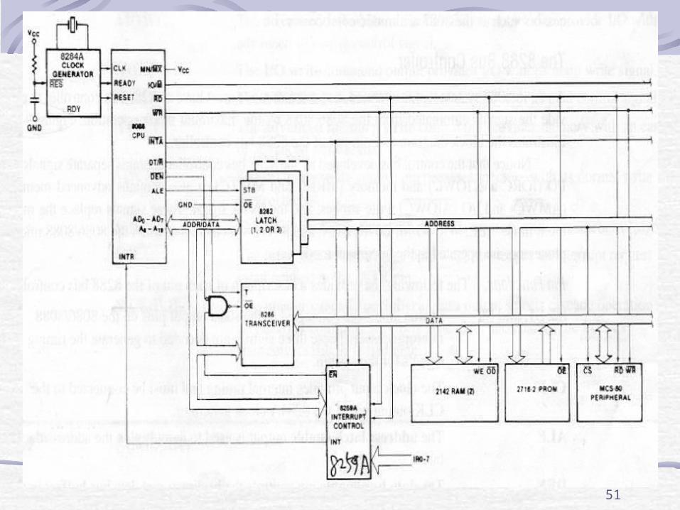
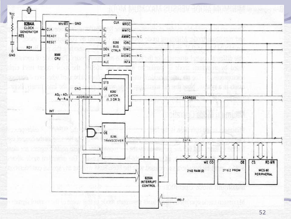
9-6 Minimum Mode versus Maximum Mode
minimum mode : Fig. 9-19(MN/MX’ = 1)similar to operation of 8085A
cost less because all control signals generated by µ
used 8-bit peripherals
maximum mode : Fig. 9-20is unique and designed to be used whenever a coprocessor(8087 arithmetic ") exist in a system
some of control signals : must generated by external 8288 bus controller
dropped from Intel family, beginning with 80286 µ
51
Fig. 9-19Fig. 9-19
52
Fig. 9-20Fig. 9-20
Ch.9 8086/8088 Hardware Specifications
53
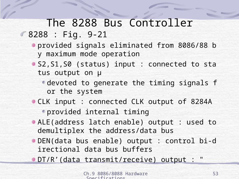
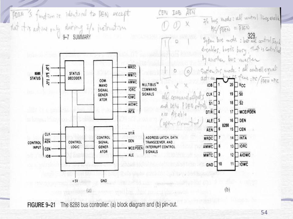
The 8288 Bus Controller8288 : Fig. 9-21
provided signals eliminated from 8086/88 by maximum mode operation
S2,S1,S0 (status) input : connected to status output on µ
devoted to generate the timing signals for the system
CLK input : connected CLK output of 8284A
provided internal timing
ALE(address latch enable) output : used to demultiplex the address/data bus
DEN(data bus enable) output : control bi-directional data bus buffers
DT/R’(data transmit/receive) output : "
54
Fig. 9-21Fig. 9-21
Ch.9 8086/8088 Hardware Specifications
55
The 8288 Bus ControllerAEN’(address enable) input : cause to enable memory control signals
CEN(control enable) input: enable the command output
IOB(I/O bus mode) input : select either system bus or I/O bus mode mode operation
AIOWC’(advanced I/O write command) output : provide I/O with its advanced I/O write control signal
IOWC’(I/O write) : provide I/O with its main write signal
IORC’, AMWC’, MWTC’, MRDC’
INTA’(interrupt acknowledge) output :
MCE/PDEN’(master cascade/peripheral data) output : select cascade operation for interrupt controller if IOB is 0, and enable the I/O bus transceivers if I/O is 1