testing guideline for single event gate rupture (segr) of ... · testing guideline for single event...
TRANSCRIPT
National Aeronautics and Space Administration
Testing Guideline for Single Event Gate Rupture (SEGR) of Power MOSFETs
Leif Scheick Jet Propulsion Laboratory
Pasadena, California
Jet Propulsion Laboratory California Institute of Technology
Pasadena, California
JPL Publication 08-10 2/08


National Aeronautics and Space Administration
Testing Guideline for Single Event Gate Rupture (SEGR) of Power MOSFETs
NASA Electronic Parts and Packaging (NEPP) Program
Office of Safety and Mission Assurance
Leif Scheick Jet Propulsion Laboratory
Pasadena, California
NASA WBS: 939904.01.11.30 Project Number: 102197
Task Number: 3.23.5
Jet Propulsion Laboratory 4800 Oak Grove Drive Pasadena, CA 91109
http://nepp.nasa.gov

This research was carried out at the Jet Propulsion Laboratory, California Institute of
Technology, and was sponsored by the National Aeronautics and Space Administration
Electronic Parts and Packaging (NEPP) Program.
Reference herein to any specific commercial product, process, or service by trade name,
trademark, manufacturer, or otherwise, does not constitute or imply its endorsement by the
United States Government or the Jet Propulsion Laboratory, California Institute of Technology.
Copyright 2008. California Institute of Technology. Government sponsorship acknowledged.
ii

TABLE OF CONTENTS 1. Introduction.......................................................................................................................1
1.1. MOSFET Basics ......................................................................................................1 1.2. Radiation Effects in Power MOSFETs: A Review and Definition of Terms..........1
1.2.1. Radiation Effects ...............................................................................................2 1.2.1.1. Dose Effects.................................................................................................2 1.2.1.2. Single-Event Gate Rupture (SEGR) and Single-Event Burnout (SEB) .....4
2. Measurement of Single-Event Gate Rupture Sensitivity ..................................................7 2.1. Applicability of Current Test Methods ...................................................................7
2.1.1. ASTM-F 1192-00 ..............................................................................................7 2.1.2. EIA/JEDC57 ....................................................................................................7 2.1.3. MIL-STD-750D ...............................................................................................7
2.2. Testing Guidelines for Evaluation of Segr Sensitivity ............................................8 2.2.1. Test Samples......................................................................................................8
2.2.1.1. Sample Selection .........................................................................................8 2.2.1.2. Number of Parts...........................................................................................8 2.2.1.3. Use of Delidded Parts..................................................................................9
2.2.2. Test Set-up.........................................................................................................9 2.2.2.1. Effect of Circuit ..........................................................................................10
2.2.2.1.1. Effect of Bias on Device Sensitivity .....................................................10 2.2.2.1.2. Effect of Power Supply on Device Segr Sensitivity..............................11 2.2.2.1.3. Thermal Stability and the Effect of Temperature..................................11
2.2.3. Irradiation Conditions........................................................................................12 2.2.3.1. Heavy Ions...................................................................................................12
2.2.3.1.1. Ion LET And Range ..............................................................................12 2.2.3.1.2. Ion Fluence............................................................................................13 2.2.3.1.3. Ion Beam Flux And Dosimetry .............................................................13 2.2.3.1.4. Ion Beam Damage .................................................................................14 2.2.3.1.5. Ion Angle...............................................................................................14
2.2.3.2. Protons.........................................................................................................14 2.2.3.2.1. Proton Energy........................................................................................14 2.2.3.2.2. Proton Fluence.......................................................................................14 2.2.3.2.3. Proton Damage......................................................................................14
2.2.4. Parts Testing Procedure .....................................................................................15 2.2.4.1. Equipment Checkout ...................................................................................16 2.2.4.2. Pre-Irradiation Data Collection ...................................................................16 2.2.4.3. Irradiation ....................................................................................................16 2.2.4.4. Post Irradiation Data Collection ..................................................................16 2.2.4.5. Segr Verification .........................................................................................16 2.2.4.6. Irradiation Run Procedure ...........................................................................17
2.2.5. Reporting ...........................................................................................................19 2.2.6. Data Analysis ....................................................................................................19 2.2.7. Testing of Related Parts.....................................................................................19
2.2.7.1. BJT ..............................................................................................................19 2.2.7.2. IGBT............................................................................................................19
iii

iv
2.2.7.3. Charge Pumps..............................................................................................19 2.2.7.4. Linear ICs ....................................................................................................19 2.2.7.5. MOSFET Drivers ........................................................................................20 2.2.7.6. Hybrid Devices............................................................................................20
2.2.8. Key Test Issues..................................................................................................20 2.2.8.1. Ion-Range Issue for MOSFETS ..................................................................20 2.2.8.2. Dose History Dependence of SEE...............................................................24 2.2.8.3. “Microbreaks” in Power MOSFETS ..........................................................26
3. Segr Rate Prediction Protocol...........................................................................................27 3.1. Limitations...............................................................................................................27 3.2. Environments...........................................................................................................28 3.3. The General Rate Equation......................................................................................28 3.4. GCR .........................................................................................................................28
3.4.1. Worst-Case Rate ................................................................................................28 3.4.2. Best-Case Rate...................................................................................................30
3.5. The Alternate Approach ..........................................................................................30 3.6. In Orbit ....................................................................................................................31 3.7. Flares .......................................................................................................................31 3.8. Rates in Mixed Operational Modes .........................................................................31 3.9. Rates and Probability...............................................................................................31
4. Alternate Testing Approaches...........................................................................................31 4.1. Laser Testing ...........................................................................................................31 4.2. Microbeam...............................................................................................................31 4.3. Simulation................................................................................................................32
5. Design Guidelines.............................................................................................................32 5.1. General Derating......................................................................................................32 5.2. Application Specific Derating ..................................................................................34
1. Introduction The use of power MOSFETs in space can be challenging due to the ubiquitous and
diverse nature of radiation that these devices encounter. Radiation can degrade the electrical properties of the device, which depending on the type and severity of the radiation can render the device non-functional. Not surprisingly, testing these devices can be complicated. Radiation testing provides a method for characterizing, or at least highlighting, radiation susceptible devices planned for use in space missions. Finally, these devices are being fabricated using evolving technologies, so keeping data timely and relevant is important.
The purpose of this document is two-fold. First, the document lists and discusses many of the issues important to understand when testing power MOSFETs. Second, the recommended approach for using radiation test data to define the device application requirements is presented. These include SEE rate calculation, data analysis, and derating guidelines. A significant amount of work has been done on the basic effects of SEB and SEGR. References are supplied where seminal work has been done on the topic at hand. The reader is urged to review the references if the testing issues or mission application at hand are complex.
1.1. MOSFET Basics Power MOSFETs are like most MOS transistors in operation and terminology [Taur01,
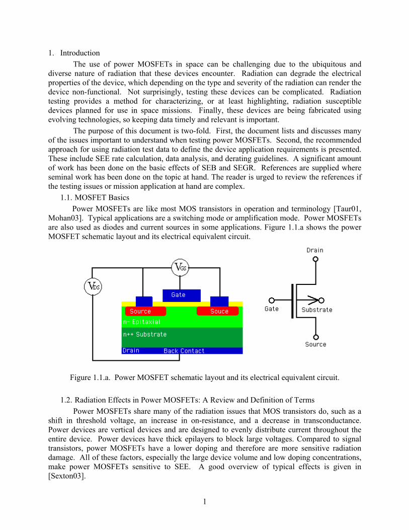
Mohan03]. Typical applications are a switching mode or amplification mode. Power MOSFETs are also used as diodes and current sources in some applications. Figure 1.1.a shows the power MOSFET schematic layout and its electrical equivalent circuit.
Figure 1.1.a. Power MOSFET schematic layout and its electrical equivalent circuit.
1.2. Radiation Effects in Power MOSFETs: A Review and Definition of Terms Power MOSFETs share many of the radiation issues that MOS transistors do, such as a
shift in threshold voltage, an increase in on-resistance, and a decrease in transconductance. Power devices are vertical devices and are designed to evenly distribute current throughout the entire device. Power devices have thick epilayers to block large voltages. Compared to signal transistors, power MOSFETs have a lower doping and therefore are more sensitive radiation damage. All of these factors, especially the large device volume and low doping concentrations, make power MOSFETs sensitive to SEE. A good overview of typical effects is given in [Sexton03].
1

1.2.1. Radiation Effects The electrical characteristics of the power MOSFET are susceptible to different types of
irradiation. Single-event effects (SEEs) are catastrophic failures, e.g., single-event burnout (SEB) and single-event gate rupture (SEGR). Following a single event like SEB or SEGR, the device will experience a high leakage current that may not be acceptable in a circuit application. On the other hand, total ionizing dose (TID) and displacement damage dose (DDD) can degrade the electrical characteristics of the power MOSFET as a function of dose.
1.2.1.1.Dose Effects TID causes the silicon dioxides (insulator regions) used in a semiconductor to trap
positive charges due to the inability of electrons to recombine with the trap charges that are caused by the ionizing radiation. These trapped charges produce a voltage within the device that affects the device’s electrical functionality. In MOSFETs, the insulating layer separates the gate from the channel, it is the oxide that is susceptible to the dose effects. Power MOSFETs, due to the vertical structure, have a more complex (i.e., non-linear) response to dose. TID effects can be caused by gamma-ray, x-ray, proton, and heavy ion irradiation, but the resulting parametric shift is not the same for each radiation type per unit dose. This relative effectiveness between types of radiation is due to the recombination difference and range differences in the energy deposition of each radiation type. Figure 1.2.1.1.a plots the shift in threshold voltage for two n-type MOSFETs. Note that for similar technology, the threshold shift of the two devices is opposite in sign. This effect is most likely due to interface traps dominating in the IRHM8450 and oxide traps dominating in the IRHMs58160.
0x100 4x10¹² 8x10¹² 1x10¹³ 2x10¹³ 2x10¹³
Proton Fluence [cm-2]
3
4
5
6
7
Thre
shol
d vo
ltage
[V]
Threshold voltage [V]VDS=10V
IRHM8450Excluding Vth=14 point
0x100 4x10¹² 8x10¹² 1x10¹³ 2x10¹³ 2x10¹³
Proton Fluence [cm-2]
3.2
3.6
4
4.4
Thre
shol
d vo
ltage
[V]
Threshold voltage [V]VDS=10V
IRHMs58160
Figure 1.2.1.1.a. Average threshold voltage for the IRHM8450 and the IRHMs58160 as a
function of proton fluence. Proton, neutron, heavy ion radiation, high energy electron and photon radiation, can
knock atoms out of lattice sites. In rare cases, the displaced atom can be transmuted by the interaction. In either case, the properties of the semiconductor material are changed and these changes, in turn, affect device electrical performance. The normal metric of this type of damage
2

is called the displacement damage dose (DDD), which is the product of the non-ionizing energy loss (NIEL) and the particle fluence. DDD shortens the carrier lifetime and reduces the carrier mobility.
On-resistance (RDSon) is an electrical parameter that is sensitive to displacement damage. DDD increases the number of crystal imperfections, which increase the material’s resistance, carrier scattering, free carrier removal, trap density and overall reduction in the diffusion length. High-voltage devices like these are lightly doped, which makes them more susceptible to DDD effects. However, DDD effects in majority carrier devices such as MOSFETs occur at a relatively high dose level. RDSon is also susceptible to TID due to the accrual of charge of the oxide in the bulk of the silicon and the interface of the oxide.
Transconductance, or transverse conductance, is the change in drain-to-source conductance with the change in the gate-to-source voltage. It is affected by both TID and DDD since it is dependent on gate and channel properties. Figure 1.2.1.1.b shows the radiation response of the forward-transconductance parameter for both IRHMS58160 and the IRHM8450.
TID and DDD effects are important to SEE testing for two main reasons. First, the shift in threshold voltage may change the channel conditions, that is, turn the device on, and this effect will change the point of SEE failure. Also, the interplay between SEE and dose effects are not well known, but a noticeable effect has been seen in [Scheick07], [Peyre06], and [Peyre07]. Therefore, dose effects must be monitored in all SEE testing. Also in [Scheick07], [Peyer06], and [Peyer07], the effect of multiple hits on the gate due to heavy ions is proposed as the driver for SEGR.
0x100 4x10¹² 8x10¹² 1x10¹³ 2x10¹³ 2x10¹³
Proton Fluence [cm-2]
4
6
8
10
12
Tran
scon
duct
ance
[S]
Tranconductance [S]VDS=10V, IDS=1A
IRHMS58160
0x100 4x10¹² 8x10¹² 1x10¹³ 2x10¹³ 2x10¹³
Proton Fluence [cm-2]
1
2
3
4
5
Tran
scon
duct
ance
[S]
Tranconductance [S]VDS=10V, IDS=1A
IRHM8450
Figure 1.2.1.1.b. Average transconductance for the IRHMS58160 and the IRHM8450.
3
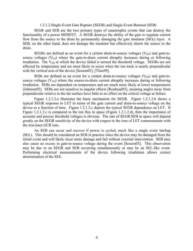
1.2.1.2.Single-Event Gate Rupture (SEGR) and Single-Event Burnout (SEB) SEGR and SEB are the two primary types of catastrophic events that can destroy the
functionality of a power MOSFET. A SEGR destroys the ability of the gate to regulate current flow from the source to the drain by permanently damaging the gate insulator (SiO2) layer. A SEB, on the other hand, does not damage the insulator but effectively shorts the source to the drain.
SEGRs are defined as an event for a certain drain-to-source voltages (VDS) and gate-to-source voltages (VGS) where the gate-to-drain current abruptly increases during or following irradiation. The VDS at which the device failed is termed the threshold voltage. SEGRs are not affected by temperature and are most likely to occur when the ion track is nearly perpendicular with the vertical axis of the device [Sexton03], [Titus99].
SEBs are defined as an event for a certain drain-to-source voltages (VDS) and gate-to-source voltages (VGS) where the source-to-drain current abruptly increases during or following irradiation. SEBs are dependent on temperature and are much more likely at lower temperatures [Johnson92]. SEBs are not sensitive to angular effects [Roubaud93], meaning angles away from perpendicular relative to the die surface have little to no effect on the critical voltage at failure.
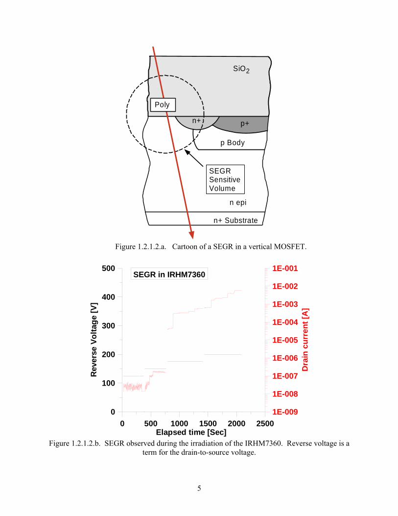
Figure 1.2.1.2.a illustrates the basic mechanism for SEGR. Figure 1.2.1.2.b shows a typical SEGR response to LET in terms of the gate current and drain-to-source voltage on the device as a function of time. Figure 1.2.1.2.c depicts the typical SEGR dependence on LET. If Figure 1.2.1.2.c is compared to the ion flux in space (Figure 1.2.1.2.d), then the importance of accurate and precise threshold voltages is obvious. The rate of SEGR/SEB in space will depend greatly on the SEGR sensitivity of the device with respect to the ions of LET commensurate with the iron knee GCR ions.
An SEB can occur and recover if power is cycled, much like a single event latchup (SEL). This should be considered an SEB in practice since the device may be damaged from the initial event and will likely incur more damage and fail without external intervention. SEB may also cause an excess in gate-to-source voltage during the event [Sexton03]. This observation may be due to an SEGR and SEB occurring simultaneously or may be an SEL-like event. Performing electrical measurements of the device following irradiation allows correct determination of the SEE.
4
SEGRSensitiveVolume
p Body
n epi
n+ Substrate
Poly
p+n+
SiO2
Figure 1.2.1.2.a. Cartoon of a SEGR in a vertical MOSFET.
0 500 1000 1500 2000 2500Elapsed time [Sec]
0
100
200
300
400
500
Rev
erse
Vol
tage
[V]
1E-009
1E-008
1E-007
1E-006
1E-005
1E-004
1E-003
1E-002
1E-001
Dra
in c
urre
nt [A
]
SEGR in IRHM7360
Figure 1.2.1.2.b. SEGR observed during the irradiation of the IRHM7360. Reverse voltage is a
term for the drain-to-source voltage.
5

0 25 50LET [MeV.cm2/mg]
75
0
50
100
150Vo
ltage
thes
hold
[V]
Conceptual SEGR/B plot
SEE response at HIGH LET
SEE response at LOW LET
SEE response in iron knee is critical
Figure 1.2.1.2.c. Conceptual response of a SEGR to LET. In many cases, the ions from
terrestrial accelerators normally used for SEE testing cannot penetrate sufficiently in the LET range of the iron knee and therefore can give imprecise results.
0 40 80LET [Me
120V.cm2/mg]
10-1110-1010-910-810-710-610-510-410-310-210-1100101102
Inte
gral
flux
[p/m
2 /s/s
t]
Figure 1.2.1.2.d. Integral heavy ion flux in deep space. The iron knee is the three decade
drop in flux from 25 to 35 MeV.cm2/mg.
6
2. Measurement of Single-Event Gate Rupture Sensitivity 2.1. Applicability of Current Test Methods
The reader is expected to have a working knowledge of an accepted single event phenomena (SEP) test standard. These are ASTM-F 1192-00, MIL-STD-750D, or EIA/JEDC57. This guideline builds upon the context of these test standards. Exceptions to these test standards are noted in this section and repeated later as applicable.
2.1.1. ASTM-F 1192-00 The American Society for Testing and Materials (ASTM) created a guide (ASTM-F
1192-00) for testing microelectronic devices using heavy ions to analyze single-event phenomena (SEPs). This guide gives a brief description of the terminology used in the radiation field.
This standard actually defers to MIL-STD-750D for power device testing. It does point out the importance of ion range when testing for SEEs. “An adequate range is especially crucial in detecting latchup, because the relevant junction is often buried deep below the active chip.” However, the guide does not clearly explain what is meant by “an adequate range.” Sections 2.2.3.1.1 and 2.2.8.1 detail this information.
2.1.2. EIA/JEDC57 The report clearly explains the requirements for testing for SEB and SEGR and how to
select the ions with which to test. Section 3.2.4, “Beam Selection,” states “Care must be taken to ensure that the penetration depth of the ion is large compared to the depth of the charge collection region. This will ensure that the beam LET is nearly constant while the ion traverses the charge collection region of the transistor.” All high-voltage power MOSFETs have a very deep substrate. Typical accelerator ions will not have a constant LET through this region.
For SEGR testing, the EIA/JEDC57 guide recommends the use of 0.1 BVDC (10% breakdown voltage) voltage increments between irradiations starting at VDS = 0 V and increasing until failure. The problem with this approach is it is too rigid. The 10% breakdown voltage step is a coarse increment that yields large error bars. We have discovered that smaller increments allow a better resolution of the domain space (the safe operating limits) of the MOSFET for the given ion.
The guide also mentions how to exercise the part between irradiations. This is important because the DUT may have gone out of specifications during the irradiation and yet still maintain electrical functionality. In the EIA guideline, most of the microbreaks (partial SEGR) would provoke an-out-of specification failure at a lower voltage.
The guide also calls for the use of an oscilloscope for SEGR testing. However, with the voltage-blocking and current-controlling abilities of current MOSFETs, this method is considered prohibitive. There are many technical issues that need to be overcome in order to use an oscilloscope with high-voltage power MOSFETs although utilizing an oscilloscope would be ideal for capturing fast events like SEGR. See Section 2.2.2.
2.1.3. MIL-STD-750D MIL-STD-750D is probably the most comprehensive of the government standards for
SEE in power devices. The section that applies to SEGR and SEB testing is Notice 3 method 1080. The major technical oversight of the document is that the definition of an event is not sensitive enough for many device failure modes. In MIL-STD-750D, gate rupture is defined as the point where the gate current exceeds the manufacturer’s rated leakage current at the gate
7

electrode. However, nothing is mentioned about the fact that transient spikes may have been observed that exceed the rated leakage current. See section 2.2.4.3.
Notice 3 highlights the required electrical resolution of the equipment for conducting SEGR and SEB testing. The resolution has to be sufficient to resolve gate currents of 10nA or less. Section 2.1 of this test protocol calls for a flux of 1x10⁵ ion/cm2 per second, and that the beam uniformity across the surface of the DUT be within ± 15%. Regarding ion range, the test method states the following: “The ion beam energy should provide sufficient ion penetration depth to induce the SEGR response…” This requirement is not specific enough to ensure that the worst case scenario for gate rupture is obtained.
The specified circuit board calls for stiffening resistors and capacitors, but fails to declare the values of each component. If all test conditions were controlled and only the resistors and capacitor values were changed, the outcome of the radiation experiment would depend on the pre-selected resistance and capacitance values. Data collected in this manner can not be compared against other data sets for which different resistance and capacitance values were selected. See section 2.2.2.
2.2. Testing Guidelines for Evaluation of SEGR Sensitivity This section outlines the procedure for determination of SEGR sensitivity. One must
remember that the final mission application of the DUT plays a large role in the test planning and implementation. For example, the test plan for a long mission duration should incorporate testing that investigates phenomena that affect reliability. Also, dynamic application conditions such as overshoots and ringing in the flight circuitry that may alter the electrical bias of the device must be considered. The electrical specifications of the device in regards to the total circuit should be known, as any degradation in the device’s electrical parameter(s) can place a large demand on power supplies leading to the addition of electrical stress on the entire circuit.
2.2.1. Test Samples Test samples for power MOSFETs will come from only a few suppliers, namely
International Rectifier (IR), Advanced Power Technology (APT), Microsemi, and ST Micro. Only IR makes total dose and single event hardened devices at this time. STM has a rad-hard version of its power MOSFETs scheduled for delivery in 2009.
2.2.1.1.Sample Selection For the test results to be most relevant to the proposed space mission, the test devices
should be from the flight lot if this is possible. Power devices are very susceptible to lot-to-lot variations and this is especially true in devices with high voltage rating. If non-flight devices are to be used, then the manufacturing differences between the test lot and flight lot must be considered. The manufacture may provide lot variance information to facilitate this evaluation. Wheatley et al illustrated the effect of lot variation for one part type to result in an appreciable variance with a correlation to reliability [Wheatley01]. See Table 5.1.a for a typical spread in effect across manufacturer and lots.
2.2.1.2.Number of Parts SEGR is a destructive test with no mitigation possible, so each data point represents a
destroyed device. Multiple parts are required both to establish part-to-part variation and remove any dose effects or partial SEE damage that can occur during testing. One or more parts are needed to identify the threshold voltage. At least five data points should be taken such that the threshold voltage can be determined to the precision required by the mission application. This
8
will result in over six parts per LET. SEB data can be taken repeatedly on the same part with proper circuit mitigation that will yield acceptable statistics as described below, but at least three parts must be used to investigate part-to-part variation. Also, localized ion damage may occur, so repeated SEBs may stress a device and result in spurious data [Sexton98], [Peyer07]. Not enough data has been gathered on this subject to bound the issue. At this time, any DUTs that exhibit any SETs or recoverable SEBs should be excluded.
A set of data should be taken for at least three different LETs as long as the ion range requirements are met. This precaution is due to the large range effect on SEGR and SEB, as well as the importance of the LET range in which the SEGR sensitivity change the most.
These part requirements sum to a test lot of at least 18 devices to in excess of 30 for widely distributed samples. If a test set consists of too few parts, or the data is too widely distributed to determine the statistical behavior of the set, then a reasonable margin should be applied to the data. Currently, no study has determined the relationship to variance in device features (e.g., oxide thickness) and radiation variance, so no method can be recommended for estimation of the voltage at which SEGR occurs for an underdetermined or poorly behaved lot. Wheatley [Wheately01] and Peyre [Peyre08] performed some statistical measurements, but no repeatable relation can be ascertained and this remains a focus of investigations.
2.2.1.3.Use of Delidded Parts Part vendors can supply delidded packages for SEE testing, otherwise parts will most
likely have to have the packaging removed for ions to reach the sensitive volume. Before packaging is removed, all devices should be measured on both a large current curve tracer, like a Tektronix 371b, and discrete device ATE, like an HP4156. After removing the packaging, identical measurements should be made to verify that the depackaging process did not alter the device performance in any way. Drain-to-source leakage will rise after any depackaging due to visible light penetrating the device producing electron hole pairs. Devices that demonstrate unstable currents or extreme light sensitivity should be rejected from the test lot. Microscopic visual inspection of the die should also be done after removal of the package for any damage or conductive debris. If a current leakage is greater than 1uA, then the part should be rejected.
Flight lot parts are usually hi-rel devices and packaged in cans. Removing the device package consists of filing or grinding the top of the can off. All leads must be grounded during this procedure and traceable ESD precautions should be used. After removal of the lid, the die may be coated in polyamide which will have to be dissolved chemically.
Plastic potting is another package type. These packages must be dissolved with a fuming acid etcher. Often the package is potted for high temperature, and therefore the package will require a very harsh acid spray to remove it. This will damage the die if exposed for too long, so great care must be taken to prevent die damage. Care must also be taken not to stress or cut bond wires in the plastic package. If the wires are cut, a micro-bonder can be used to reattach the wires.
2.2.2. Test Set-up The test circuit should be constructed to be worst case based on the mission application.
If the mission in question contains multiple applications, each application should be tested or a worst case for each application should be identified and tested. Higher bias, higher temperature, higher duty cycle, and lower application tolerances are all worst case for SEGR [Sexton03].
9
2.2.2.1.Effect of Circuit The test circuit will contain resistances, capacitances, and inductances that affect the SEE
characteristics. Each parameter should be measured or at least designed in the test system to present a minimal effect on the test. Overall, it is better to reduce the overall length of all cabling to reduce variance in test parameters. The power supply should be placed as near as possible to the test site with minimal cable length. The heavy ion accelerator environment will not produce a significant amount of radiation to induce dose effects or SEE in the power supplies or computers. A proton beam, however, will produce a significant neutron background. If the power supply can not be operated remotely, then the effects of the cabling should be carefully noted.
The test board for the DUT and the daughter board (if used) will add extra capacitance that will act as a bypass or stiffening capacitor. This will increase the sensitivity of SEB. So if any inductance has been added to retard SEB, accidental board capacitance will enhance the effect. Added board capacitance can filter out charge collection noise or transient events. If observations of such events are desired, the test probes should be placed before the capacitance or capacitance should be minimized. Test point probe cabling to oscilloscopes should, of course, be low impedance and capacitance.
Test cabling will induce an amount of inductance that will retard SEB and transient effects. Stiffening capacitance should be added to increase SEB sensitivity, if needed. At least 250 uF should be used for this purpose.
2.2.2.1.1. Effect of Bias on Device Sensitivity Device bias is the primary independent variable for SEE testing. It is critical that a DC
power supply with a low ripple be used. If a stable power supply is not used; the highest possible voltage should emulate the device rated voltage. Many institutions, including the one that authored this guide, will reject test data taken with an unstable power supply. In that vein, the effect of any interface with the bias at the device due to EM coupling or snapback in the circuit in the device must be known. If a device is accidentally exposed to a greater than rated voltage, SEE sensitivity can be increased, and therefore should be rejected from the test lot.
The definition of SEE threshold voltage for a part is defined as the highest voltage at which the device exhibited no SEE. This definition highlights the importance of testing several devices and refining the starting voltage bias increments of the test. As noted in section 2.2.1.2, at least five parts should be taken at the highest starting voltage and lowest increment for the desired precision to ensure all uncertainties are bounded.
The SEGR will occur at a certain combination of the drain-to-source and gate-to-source voltage. The SEGR threshold at both voltages is the required metric. The gate voltage will affect SEE more in lower voltage devices. Table 2.2.2.1.1.a shows the most methodical way to scan thorough the possible combinations of Vds and Vgs. The table assumes that Vds(1) occurs at a low enough voltage that no SEGR occurred. The tester is expected to refine and amend the flow according to the previous device test. Table 2.2.2.1.1.b is the recommended path if SEB is present.
10

Table 2.2.2.1.1.a. Recommended approach for multiple bias testing when SEB is suppressed or not an issue for part at hand.
Vgs= 0V ±5V ±10V ±15V ±20V
Vds(1) Vds(2) Vds(3) Vds(n-1) Vds(n)
Table 2.2.2.1.1.b. Recommended approach for multiple bias testing when SEB is an issue or
suspected for the part.
Vgs= 0V ±5V ±10V ±15V ±20V
Vds(1) Vds(2) Vds(3) Vds(n-1) Vds(n)
2.2.2.1.2. Effect of Power Supply on Device SEGR Sensitivity
The power supply must be able to supply the needed current while constantly supplying the correct voltage for each pin. SEGR in general does not need an excessive amount of current to mature the effect, while SEB does. The power supply must be able to apply the needed voltage regardless of the charge collection noise or EM interference of the facility.
2.2.2.1.3. Thermal Stability and the Effect of Temperature In general, the temperature of a DUT in a SEE test will not increase due to power
dissipation since the actual SEE testing requires the device to be in the off mode and the current in the device will be very low. When the device does fail, however, the temperature will increase, but the test is over. So testing that solely investigates the SEE and no other effect can be done without thermal management.
If the device is on (i.e., the device conducts any more than background current) during any portion of the testing, then device temperature may increase. The effects of temperature on SEGR and SEB have been studied [Sexton03], [Johnson92], [Mouret94], as well as the effects of temperature on the reliability and lifetime of damaged devices [Scheick07]. These references show the damage type and magnitude, like breakdown from latent damage, correlated with irradiation and operation temperature. Therefore, value may be added by operating the device in the on mode between ion irradiations to include worst case. But, if the thermal stress step is
11
added to the test step, the temperature should be precisely measured (including taking thermal diffusion times into account) and actively managed. This reliability check of stressing the device with high current is not, however, recommended in the beam since the current levels will overstress most delicate SEE test fixtures. If high current stress tests are required, the parts are recommended to be removed between irradiation and tested on a dedicated ATE like a Tektronix 371b. The device will increase in temperature and should be allowed to cool to the desired test temperature before return to test, a process that can be understandably time prohibitive. SEB likelihood decreases with increasing temperature, so any SEB testing must be done at a controlled temperature.
2.2.3. Irradiation Conditions As a general rule, note anything that could affect the testing. These affecters include but
are not limited to temperature, light level, air gap in beam (if testing in air) and physical observation of the die at irradiation.
2.2.3.1.Heavy Ions The energies required to penetrate most power devices will allow for the irradiation to
occur in open air with minimal change in LET and straggling effects. Many test setups will require the distance from the test board to be several inches away from the end of the beam line, and if this is the case, this should be noted in the test log directly or in the layers file (e.g., if at TAM) to calculate LET change and variance.
2.2.3.1.1. Ion LET and Range At least three different LETs should be used if ion range permits. At least one LET
should be done at the LETs above the iron knee of the GCR flux. This range of LET values is important since it represents the transition of high flux to low flux LETs, as well as being an LET that can induce partial damage (See section 2.2.8.3.). One LET should be done below the iron knee.
If a device is thick, the ions should be selected with no degrading at all. Degraded beams will induce straggling and add more uncertainty to the threshold voltage measurement.
It is advisable to investigate the mission application of the proposed DUT and test at the LET for which the largest LET ion will hit the device to the desired survival probability. This is because many unpredicted effects occur at the higher LETs. The probability of hitting the gate area of the device can be extracted from Figure 1.2.1.2.d by calculating the rate of strikes on the gate area for the mission length.
Heavy ion irradiation should be done at a facility that provides ions of enough range to penetrate the device from the top of the device (the gate region) to a depth of half the bulk silicon region. Table 2.2.3.1.1.a shows these ranges for typical devices. If the device has a thinner substrate than the estimated values in Table 2.2.3.1.1.a, the ion range can be reduced accordingly. Section 2.2.8.1 discusses the ramification and the treatment of data for tests using ions of insufficient range.
If a particular LET is required for testing, the ion with the longest range should be used since range in the device is a critical parameter. If the device is thinner than the range of the ions in question, then a test with each ion at the LET in question should be done to observe the dependence.
12
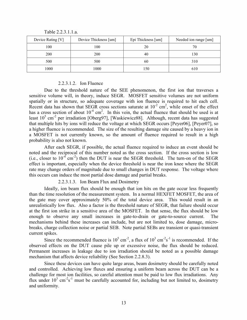
Table 2.2.3.1.1.a. Device Rating [V] Device Thickness [um] Epi Thickness [um] Needed ion range [um]
100 100 20 70
200 200 40 130
500 500 60 310
1000 1000 150 610
2.2.3.1.2. Ion Fluence
Due to the threshold nature of the SEE phenomenon, the first ion that traverses a sensitive volume will, in theory, induce SEGR. MOSFET sensitive volumes are not uniform spatially or in structure, so adequate coverage with ion fluence is required to hit each cell. Recent data has shown that SEGR cross sections saturate at 10-2 cm2, while onset of the effect has a cross section of about 10-4 cm2. In this vein, the actual fluence that should be used is at least 105 cm-2 per irradiation [Oberg97], [Waskiewicz88]. Although, recent data has suggested that multiple hits by ions will reduce the voltage at which SEGR occurs [Peyer06], [Peyer07], so a higher fluence is recommended. The size of the resulting damage site caused by a heavy ion in a MOSFET is not currently known, so the amount of fluence required to result in a high probability is also not known.
After each SEGR, if possible, the actual fluence required to induce an event should be noted and the reciprocal of this number noted as the cross section. If the cross section is low (i.e., closer to 10-4 cm-2) then the DUT is near the SEGR threshold. The turn-on of the SEGR effect is important, especially when the device threshold is near the iron knee where the SEGR rate may change orders of magnitude due to small changes in DUT response. The voltage where this occurs can induce the most partial dose damage and partial breaks.
2.2.3.1.3. Ion Beam Flux and Dosimetry Ideally, ion beam flux should be enough that ion hits on the gate occur less frequently
than the time resolution of the measurement system. In a normal HEXFET MOSFET, the area of the gate may cover approximately 50% of the total device area. This would result in an unrealistically low flux. Also a factor is the threshold nature of SEGR, that failure should occur at the first ion strike in a sensitive area of the MOSFET. In that sense, the flux should be low enough to observe any small increases in gate-to-drain or gate-to-source current. The mechanisms behind these increases can include, but are not limited to, dose damage, micro-breaks, charge collection noise or partial SEB. Note partial SEBs are transient or quasi-transient current spikes.
Since the recommended fluence is 105 cm-2, a flux of 103 cm-2s-1 is recommended. If the observed effects on the DUT cause pile up or excessive noise, the flux should be reduced. Permanent increases in leakage due to ion irradiation should be noted as a possible damage mechanism that affects device reliability (See Section 2.2.8.3).
Since these devices can have quite large areas, beam dosimetry should be carefully noted and controlled. Achieving low fluxes and ensuring a uniform beam across the DUT can be a challenge for most ion facilities, so careful attention must be paid to low flux irradiations. Any flux under 103 cm-2s-1 must be carefully accounted for, including but not limited to, dosimetry and uniformity.
13

2.2.3.1.4. Ion Beam Damage Heavy ion irradiation will induce both total ionizing dose (TID) and displacement
damage (DDD) in the DUTs. Further more, heavy ions with a high atomic number will be more likely to cause a large amount of DDD and micro-fractures in the gate oxide, causing small amounts of leakage. Normally, the dose to a material is described by these relations:
TID=LET*Fluence, and DDD=NIEL*Fluence, where fluence is the number of particles per unit area and NIEL is the non-ionizing
energy loss. Rad-hard power MOSFETs may be specified for 100 to 1000 krad(Si), while COTS parts and non rad-hard parts may only be good to 1 krad(Si). A DUT should be removed from test when the dose to the parts exceeds the estimated DUT radiation hardness or the device starts to show the effect of TID or DDD damage (see section 1.2.1). Parts that are removed from the test flow must not be considered parts that pass an SEGR irradiation.
2.2.3.1.5. Ion Angle An extensive amount of research has been done on the effect of ion angle on SEGR. The
worst-case scenario for SEGR is when the ion path is parallel with the vertical axis of the DUT. All SEGR testing should be done with the ion beam at this same relative angle. The tolerance for ion beam angle should be within ±5 degrees of normal incidence [Mouret94], [Kirsh98], [Sexton98]. If angular data in needed, careful attention must be paid to the effective range of the ion.
2.2.3.2.Protons Protons can cause SEB in very high voltage devices [Oberg96]. And, it has been seen
that protons could induce SEGR in vulnerable devices so they are included in this guideline [Titus98]. Neutrons also cause SEB [Normand97]. Protons will induce SEE in devices due to the spallation reaction of a proton and a lattice atom, as opposed to the LET of the proton itself. Therefore, the cross section of a proton induced SEE will be much lower than the heavy ion cross section [Koga96].
2.2.3.2.1. Proton Energy Proton energies must be at least as high as the maximum energy seen in the mission
environment. In fact, test energies should be higher than in the mission environment by a factor of two. This is due to the considerable changes in secondary particle from proton induced nuclear reactions as a function of energy [Srour03], [Srour06]. Any proton SEE testing must be done at energies greater than 7 MeV, since this is the threshold of proton induced nuclear reactions [Srour06].
2.2.3.2.2. Proton Fluence Since the cross section of SEE from protons for power devices is not well known, a test
fluence should reflect the expected mission fluence and the relative expected risk to the mission. 2.2.3.2.3. Proton Damage
During SEE testing with protons, constant monitoring of critical device parameters like threshold voltage and transconductance should be performed to ensure that the device damage has not changed the DUT’s electrical parameters. This is especially true for threshold voltage in n-channel devices since TID will reduce the threshold voltage and the device may enter the
14

saturation or linear region, change charge collection characteristics, and therefore SEE sensitivity [Koga96], [Sexton98], [Scheick07].
It is advisable to include parametric measurement equipment to make device measurements during SEGR testing to monitor devices in between heavy runs. Behavior in the subthreshold region will be especially indicative of device parameters changing with irradiation [Scheick07].
2.2.4. Parts Testing Procedure Figure 2.2.4.a shows the basic strategy in testing a group of power MOSFETs for
SEGRs. Fundamentally, each meaningful tested device must have at least one irradiation with no SEGR. To refine precision of the threshold voltage measurement, DUTs are tested at higher starting voltage and smaller voltage increments.
Select initial biases. Select bias increments. Select ion species. Select flux. Select number of test per ion.
Start
Fails at initial voltage? Reduce initial
bias.
Test DUT as in Figure 2.2.4.6.a.
Stop
Change ion beam.
Tested requisite # of
parts?
Select new part. Increase initial bias closer to SEE threshold and decrease bias steps.*
Another ion beam?
*That is, change the starting bias and change in bias steps to reduce the dose on the part and increase precision in the SEGR threshold
Yes
Yes
Yes
No
No
No
Figure 2.2.4.a. Flow chart for strategy of SEGR testing of a sample of parts.
15

2.2.4.1.Equipment Checkout When installed in the beam, the measurement equipment should be able to measure
benchmark parameters of the device, e.g., threshold voltage, RDSon, transconductance, etc. A test circuit or calibration DUT should be used to verify that the equipment can measure the correct voltage, current and timing. Timing can be verified by pulsing a calibration MOSFET gate on and capturing the current response in the equipment.
2.2.4.2.Pre-Irradiation Data Collection Before each irradiation, a baseline current measurement between all terminals (drain-to-
source (IDS), drain-to-gate (IDG), gate-to-source (IGS)) should be performed. 2.2.4.3.Irradiation
Beam irradiation should occur after biases are applied and currents have stabilized to baseline conditions. Beam irradiation will induce charge collection noise similar to a silicon barrier detector response [Koga96]. Figure 1.2.1.2.b is an example. If an automatic compliance function is incorporated into the test system, the definition of an SEGR is an event that sustains an IGD current over the defined limit, as opposed to a short duration spike in the current from charge collection. Charge collection noise that is highly variable, that is with sporadic large spikes, may be due to SEB events that are suppressed by the inductance of the local circuit. If any leakage current is seen to monotonically rise due to irradiation, this may be due to a dosing effect and should be verified out of the beam.
When the current is seen to rise and remain above the compliance limit, the ion beam should be removed and the total fluence for the run should be recorded. The device should remain powered for at least 100 measurements or 5 seconds, which ever is smaller, so that the effect can stabilize. The device should be powered down after the data is recorded.
2.2.4.4.Post Irradiation Data Collection Between irradiations the device should be powered and monitored to investigate any
parametric shift or change in device behavior. This is best accomplished by acquiring a set of IV and transconductance curves using the SEGR/B test system or a curve tracer. A device that exhibits a significant shift in device parameters (including but not limited to leakage current, gate voltage threshold, transconductance), it should be excluded from the test and the TID and DDD on the device should be noted. A significant shift in device parameters implies a threshold damage event and has been shown to affect charge collection which may interfere with SEE [Koga96], [Scheick07]. During checkout, the devices should be powered at maximum allowable voltages in the off position to verify that the part can withstand its rated voltage. If desired, the maximum current limit can be applied through the device to also confirm device integrity. Please review section 2.2.2.1.3 on thermal management if performing this test between irradiations.
2.2.4.5.SEGR Verification If an SEGR is suspected, the post irradiation data collection should verify that IGD or IGS
is above the compliance limit. It has been seen in the literature that a recoverable condition of high current in the device is seen due to SEE [Sexton03]. This phenomenon is related to SEL in CMOS devices. If the device is seen to recover and operate normally, the event should be noted but not as a SEGR or SEB. This device can continue as a test DUT if no evidence of damage is seen.
16

2.2.4.6.Irradiation Run Procedure The basic strategy for SEGR, or any voltage threshold testing, is to initiate the first
irradiation at a bias lower than the SEGR threshold and increase bias and increment bias for each subsequent irradiation. When an abrupt rise in gate current of the defined magnitude occurs, the event is noted along with beam dosimetry and resulting leakage current. Figure 2.2.4.6.a shows the procedure for a single part.
17

Apply Initial VDS and VGS. Measure currents.
Start
Verify transistor characteristics
Expose DUT to beam. Monitor all bias and currents.
SEE during beam?
Remove beam. Monitor all bias and currents for 5 seconds.
Remove all biases.
Apply same VDS and VGS. Measure currents. Apply max VDS and VGS. Measure currents.
Verify transistor characteristics
SEE after beam?
Test DUT again?
Increment bias as in Table 2.2.2.1.1.a. or 2.2.2.1.1.b
Stop
Stop beam. Remove biases. Note fluence and other beam metrics
Apply same VDS and VGS and verify SEE.
SEE verified?
Use DUT for another test if DUT is fine. *
*This may be a SEL like effect. The phenomenon should be considered a mission threatening SEE, but more testing may be apt.
Beam on period
Yes
Yes
Yes
Yes
No
No
No
No
Figure 2.2.4.6.a. Flow chart for SEGR testing of a single part.
18
2.2.5. Reporting All device and beam dosimetry measurements should be recorded in tabular format. All
events of each irradiation bias level (including but not limited to microbreaks, SEL types events, transients) should be recorded to be evaluated for the reliability and circuit impact of the device.
2.2.6. Data Analysis The final product of an SEE test of power devices is a series of three scatter plots relating
the following variables: gate-to-source voltage, drain-to-source voltage, and LET. This should be done for each level of SEGR and other effects if required. The mission application will drive what phenomena should be noted. For example, if the mission application has no ability to cycle power, any high current state should be noted since this may burnout the device.
Strip chart data of the voltages and currents should also be graphically presented to investigate the effect on charge collection phenomena. A Fourier transform of the strip chart data can reveal whether or not the jitter in the current is flicker-like, which implies no major SEE precursors have occurred.
2.2.7. Testing of Related Parts Many devices exhibit SEGR and SEB, or very similar SEE phenomena. The testing
processes outlined in this guide will apply with the exceptions noted in this section. 2.2.7.1.Bipolar Junction Transistor (BJT)
Power BJTs will only exhibit SEB, so the same approach as SEB measurements of MOSFETs will apply. Inductance of the local circuit will greatly affect the SEB sensitivity of the device.
2.2.7.2.Insulating Gate Bipolar Transistor (IGBT) An IGBT is a BJT in which a MOSFET controls the base current. The device has some
of the advantages of both devices. It can be a monolithic device or a hybrid. Monolithic devices can be tested exactly like a power MOSFET, although the exact failure mode may be impossible to identify. Hybrid devices are two discrete devices that are potted in a discrete package. They can be tested by depackaging the device and severing the circuit connection to test them directly [Becker06]. Testing then should emulate a BJT test or MOSFET test. IGBTs are typically used to block several thousand volts, and have been shown to be very susceptible to radiation [Selva06].
2.2.7.3.Charge pumps Charge pumps will exhibit SEDR (single event dielectric rupture) which is very similar
to SEGR [Nguyen99]. Dielectric rupture is very dependent on the applied field, like SEGR, but in the devices of interest, namely flash memories, the biases will be fixed so the testing is more like typical SEU testing. SEDR can be very sensitive to angle [Lum04], [Swift96].
2.2.7.4.Linear ICs The OP484 and the OP27 have exhibited an SEDR in the reference capacitor under
certain bias conditions [Boruta01], [Lum00], [Lum04]. If a device is susceptible to such effects and the application is high bias, then SEDR is possible. The failure of device functionality is the critical metric, so the supply current and other parameters may not be useful parameters to measure. Likewise, any partial or microscopic damage can not be readily discerned from measuring the current on the device pins.
19

2.2.7.5.MOSFET Drivers MOSFET drivers, and other driver ICs, are basically buffers that have an output stage
designed to drive a higher current at high slew. The output stage often is designed much like a power MOSFET so the SEE susceptibility is similar. Drivers also have the ability to be biased at different levels, so testing the driver is nearly identical to power device testing. One notable exception is the dependence of the SEE sensitivity on the logical state of the driver. Therefore, the SEE sensitivity should be tested in the worst case mission applications, if not all of the permutations of device conditions. These drivers also usually have CMOS control and routing logic, so SEL may occur concurrently with other SEE.
2.2.7.6.Hybrid Devices Hybrid devices of interest include but are not limited to DC-DC converters, some IGBTs
(discussed above), and discrete charge pumps. When these devices contain power devices for testing, the best method for test is to remove the device of interest and test as one would a discrete device. If this approach is not viable, then testing can be done on the device as a whole. The failure of device functionality is the critical metric and the device circuit will tend to obscure any leakage, so the supply current may not be a useful parameter to measure. And since that is true, any partial or microscopic damage can not be readily discerned by measuring the current on the device pins.
2.2.8. Key Test Issues Power devices have become very complicated and several exigencies have been
discovered. This section outlines many of the major observations that have affected these devices in recent test efforts.
2.2.8.1.Ion-Range Issue for MOSFETs One of the fundamental challenges facing power-device radiation effects is the limited
range of terrestrial ions available for testing. Texas A&M University, Grand Accélérateur National d'Ions Lourds (Large National Accelerator for Heavy Ions—GANIL), and Michigan State University cyclotrons have the highest energy per nucleon of beams with which to currently test, and the ions from these facilities have ranges on the order of 300 μm in Si. The drain-to-gate depth of the largest rated voltage devices is over 400 μm. The lightly doped region is about 25 μm for 200-V devices, 50 μm for 500-V devices and 120 μm for 1000V devices. Ions from these facilities cannot penetrate the entire charge-sensitive region of the MOSFET, so SEE characteristics can be quite different from what would be expected in a Galactic Cosmic Ray (GCR) environment. For example, Figure 2.2.8.1.a shows a typical SEGR curve for an older, thinner power MOSFET. The ions almost completely penetrate the device, and the voltage at which SEGR occurs decreases with LET in a concave curvature. This is in contrast to Figure 2.2.8.1.b, which shows ions whose range cannot entirely penetrate the 120-μm lightly doped region of the 1000-V device. Two sets of data are shown in the figure: data recorded by the manufacturer at the BNL TVDG Accelerator, and measurements made at Texas A&M. The figure shows that ion range affects test results, overestimating failure voltages for short-range ions.
20

0
20
40
60
80
100
120
140
0 20 40 60 8
LET (MeV-cm2/mg)
SEG
R B
reak
dow
n Vo
ltage
0
115 V Power MOSFET
Figure 2.2.8.1.a. A typical SEGR curve for an older, thinner power MOSFET
0
200
400
600
800
1000
0 10 20 30 40 50 6LET (MeV-cm2/mg)
Volta
ge fo
r Gat
e R
uptu
re
0
Manufacturer's data with short-range ionsData with long-
range ions
Figure 2.2.8.1.b. 1000-V device with ions of two different ranges.
21

0
10
20
30
40
50
60
70
0 5 10 15 20 25 30 35 40 45 50Penetration (µm)
wei
ghte
d av
e. L
ET
(MeV
cm
2 /mg)
I127
Xe129
Nb93 Br79
Mo106
Oxide
15 um Epi26 um Epi 40 um Epi
Figure 2.2.8.1.c. Weighted average LET (MeV cm2/mg) for swift heavy ions traveling through a virtual power MOSFET composed of 3 um of metallization over 75 Å of SiO2 and a Si epitaxial layer of various depths, i.e., 15, 26 and 40 um. The ions used in this study are similar to the short range ions from Brookhaven National Laboratory and the long range ions from Texas A&M.
Figure 2.2.8.1.c represents the weighted average LET for short range ions versus long
range ions. Energy deposited in a deep epitaxial structure of a power MOSFET by short range ions is less than the energy deposited by long range ions, as can be seen from the area under the curves for I127 vs. Xe129 or Br79 vs. Nb93. The geometry used for this study was based on cross sectional cuts of vertical MOSFETs. A power MOSFET rated at 100 V has an epitaxial depth of about 15 um, a 200 V MOSFET has an epitaxial layer of about 26 um and a 400 V corresponds to an epitaxial layer of 40 um. A 1000 V power MOSFET has an epitaxial layer in excess of 100 um. The ions selected for this computational study are identical to the ions that are available to researchers at Brookhaven National Laboratory (BNL) and Texas A&M University (TAM).
Figure 2.2.8.1.d illustrates a very important phenomenon that can lead to gross errors in mission assurance. Note in the figure that the most damaging ion of the three tested (that is, the lowest bias at which SEGR occurs) in not the largest LET ion, but with the ion with the second longest range and second highest LET. These data highlight the sensitivity of the SEGR effect to range.
Figure 2.2.8.1.e shows a similar effect for a 200-V power MOSFET, which is a relatively low-voltage device. The change in the voltage at which SEGR occurs as the ion range goes from short to long may be up to 50% of the rated voltage, e.g., a 400 V device that fails at 350 V with short range ions could exhibit SEGR at 150 V with ions with twice the range of the epitaxial layer.
Figure 2.2.8.1.f shows a first-order illustration of the effect of the range of an ion on the voltage at which SEGR occurs. The abscissa metric is the ratio of penetration distance of the ion
22

into the MOSFET between two ions of approximately 37 MeV/mg/cm2. One ion was produced at BNL with a range of approximately 35 um and the other was produced at TAM with a range of 250 um. This metric is solely geometric, but does show that the range effects in SEGR are non-negligible and are more severe for high voltage devices. This has been addressed only topically in the literature [Selva99].
0 -5 -10 -15 -20Gate-to-source [V]
0
50
100
Dra
in-to
-sou
rce
[V]
SEE for IRHF58160Bromine 36.7MeV-cm2/mg 39.5 um Iodine 59.8MeV-cm2/mg 32.5 umGold 82.3MeV-cm2/mg 28.4 um
Figure 2.2.8.1.d. SEGR data that shows that the effect can be more sensitive to range than LET.
20 24 28 32 36 40LET [MeV.cm2/mg]
0
40
80
120
160
200
V DS [
V]
IR Data: Pass with Ids < 1e-3AJPL data: Pass with Ids < 1e-3A
Figure 2.2.8.1.e. Test data for the same device at Brookhaven National Laboratory (O) and at Texas A&M University (X). The range of the 28-MeV.cm2/mg data point is 83 μm at Brookhaven and 137 μm at Texas A&M while the range of the 38-MeV.cm2/mg data point is 43
23

μm at Brookhaven and 252 μm at Texas A&M. Although these parts had different date codes, they were similar enough to observe the drop in SEGR voltage with longer-range ions.
1 1Ratio of ion penetration for two ions
of same LET
01
10
100
1000Sh
ift in
SEG
R v
olta
ge
100
200
500
1000
SEGR voltage shift vs. Ion pentrationin power MOSFETs for
ions of LET~37 MeV/mg/cm2and ranges =~40um and 250um
Figure 2.2.8.1.f. The effect of different range ions of the same LET on the SEGR voltage for four MOSFETs of various voltage ratings.
2.2.8.2.Dose History Dependence of SEE
To study how harsh mixed radiation environments affect the SEE propensities of the devices, data in which devices were dosed with various radiation types were analyzed. SEE characteristics were generally unchanged, for doses lower than 2 × 1013 cm-2 of protons and neutrons. Pre-irradiation with both gamma and proton irradiation did not drastically lower the SEGR voltage of the MOSFET. This was a fairly unexpected result since the changes in electric field lines due to radiation should have affected the breakdown characteristic of the devices. The 100V abscissa point was extrapolated from the data set, and thus has larger error bars. Also, dose shows a slight decrease in the SEGR voltage for parts that have been heavily irradiated.
Figure 2.2.8.2.a respectively plots the valid data points that met the “last-pass” criteria for the IRHM8450 and IRHM58160. The y-axis represents the critical voltage (Vcr), which was determined by computing the arithmetic average of the “last pass” voltage and the voltage at “failure.” The error bars were determined as being half the voltage increment (ΔV/2) between the “last pass” and the “failure” point. The x-axis represents the ion LET (MeV cm2/mg) at the
24

surface of the die. The gate voltage for all runs was 0 V. This response was similar but less dramatic than results seen for the IR G30 1000-V MOSFETs.
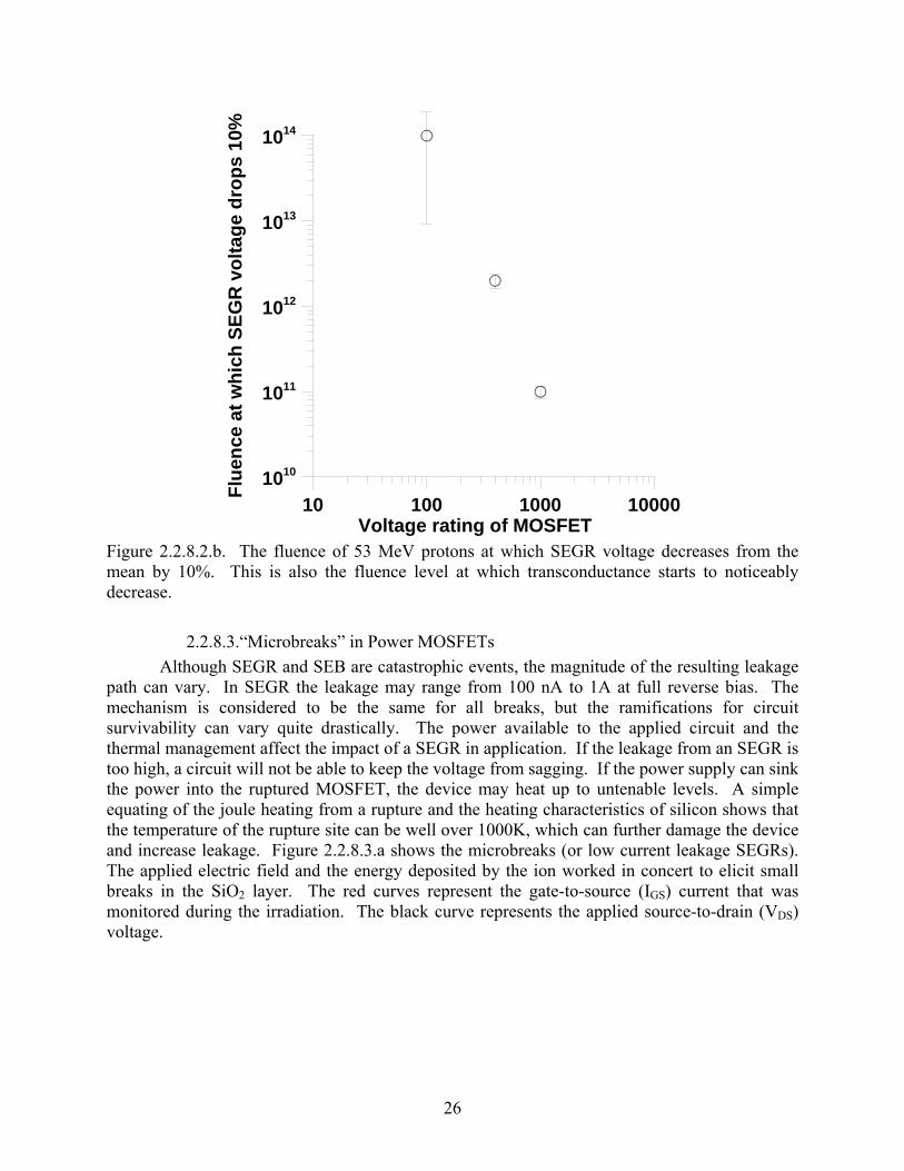
Figure 2.2.8.2.b compiles the aforementioned examples into one comparative graph. There is an obvious relationship between total irradiation level and the voltage at which a device exhibits SEE. Essentially high voltage devices, due to their low doping and large features, are more susceptible to the effect. The dose level at which the 1000V device experiences damage is typical of missions to Mars, Jupiter, Lagrangian points and Earth orbiters.
0x100 4x10¹² 8x10¹² 1x10¹³ 2x10¹³ 2x10¹³
Fluence [cm-2]
0
100
200
300
400
500
V DS [
V]
IRHN8450VGS=0V Last pass
LET = 20 MeV.cm2/mgLET = 32 MeV.cm2/mgLET = 39.8 MeV.cm2/mg
Figure 2.2.8.2.a. Radiation response of the IRHN8450 power MOSFET.
25
10 100 1000 10000Voltage rating of MOSFET
1010
1011
1012
1013
1014
Flue
nce
at w
hich
SEG
R v
olta
ge d
rops
10%
Figure 2.2.8.2.b. The fluence of 53 MeV protons at which SEGR voltage decreases from the mean by 10%. This is also the fluence level at which transconductance starts to noticeably decrease.
2.2.8.3.“Microbreaks” in Power MOSFETs
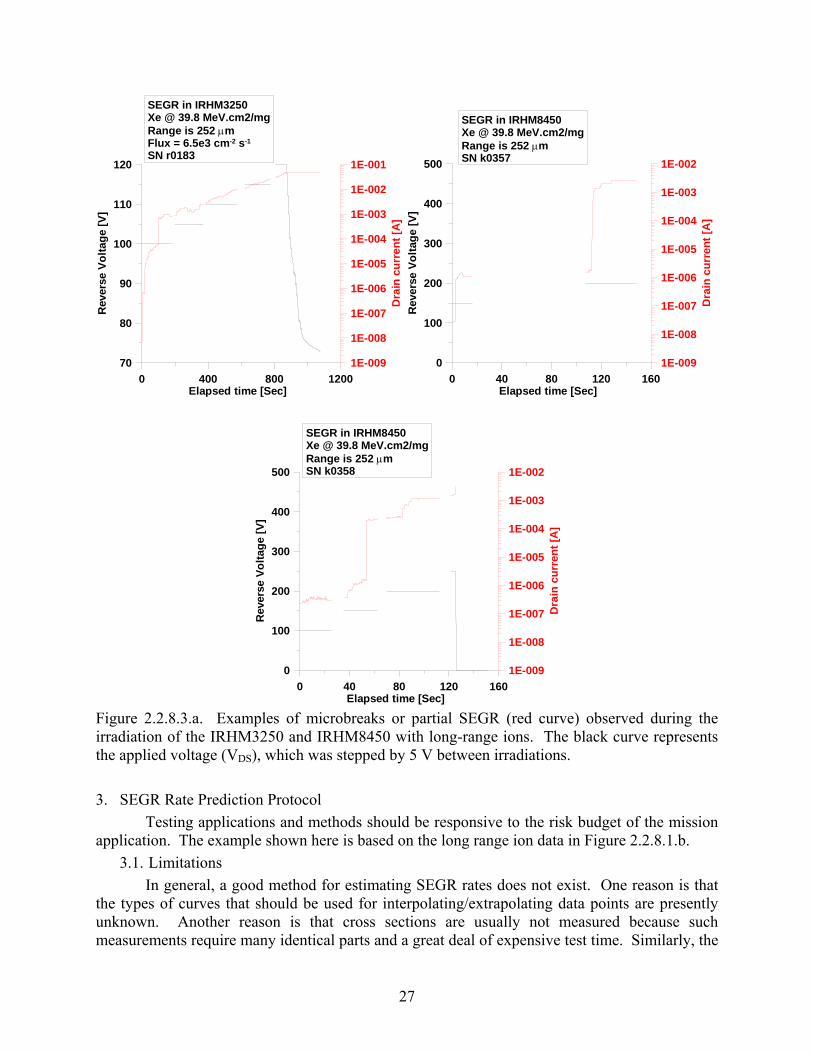
Although SEGR and SEB are catastrophic events, the magnitude of the resulting leakage path can vary. In SEGR the leakage may range from 100 nA to 1A at full reverse bias. The mechanism is considered to be the same for all breaks, but the ramifications for circuit survivability can vary quite drastically. The power available to the applied circuit and the thermal management affect the impact of a SEGR in application. If the leakage from an SEGR is too high, a circuit will not be able to keep the voltage from sagging. If the power supply can sink the power into the ruptured MOSFET, the device may heat up to untenable levels. A simple equating of the joule heating from a rupture and the heating characteristics of silicon shows that the temperature of the rupture site can be well over 1000K, which can further damage the device and increase leakage. Figure 2.2.8.3.a shows the microbreaks (or low current leakage SEGRs). The applied electric field and the energy deposited by the ion worked in concert to elicit small breaks in the SiO2 layer. The red curves represent the gate-to-source (IGS) current that was monitored during the irradiation. The black curve represents the applied source-to-drain (VDS) voltage.
26
0 400 800 1200Elapsed time [Sec]
70
80
90
100
110
120
Rev
erse
Vol
tage
[V]
SEGR in IRHM3250Xe @ 39.8 MeV.cm2/mgRange is 252 μmFlux = 6.5e3 cm-2 s-1
SN r0183
1E-009
1E-008
1E-007
1E-006
1E-005
1E-004
1E-003
1E-002
1E-001
Dra
in c
urre
nt [A
]
0 40 80 120 160Elapsed time [Sec]
0
100
200
300
400
500
Rev
erse
Vol
tage
[V]
SEGR in IRHM8450Xe @ 39.8 MeV.cm2/mgRange is 252 μmSN k0357
1E-009
1E-008
1E-007
1E-006
1E-005
1E-004
1E-003
1E-002
Dra
in c
urre
nt [A
]
0 40 80 120 160Elapsed time [Sec]
0
100
200
300
400
500
Rev
erse
Vol
tage
[V]
SEGR in IRHM8450Xe @ 39.8 MeV.cm2/mgRange is 252 μmSN k0358
1E-009
1E-008
1E-007
1E-006
1E-005
1E-004
1E-003
1E-002
Dra
in c
urre
nt [A
]
Figure 2.2.8.3.a. Examples of microbreaks or partial SEGR (red curve) observed during the irradiation of the IRHM3250 and IRHM8450 with long-range ions. The black curve represents the applied voltage (VDS), which was stepped by 5 V between irradiations.
3. SEGR Rate Prediction Protocol
Testing applications and methods should be responsive to the risk budget of the mission application. The example shown here is based on the long range ion data in Figure 2.2.8.1.b.
3.1. Limitations In general, a good method for estimating SEGR rates does not exist. One reason is that
the types of curves that should be used for interpolating/extrapolating data points are presently unknown. Another reason is that cross sections are usually not measured because such measurements require many identical parts and a great deal of expensive test time. Similarly, the
27

directional dependence of device susceptibility (which is different for different part designs) is usually not measured. Therefore, instead of an accurate rate estimate, two estimates are defined as follows:
Worst Case ≡ Almost certainly too large. Best Guess ≡ Almost certainly containing some uncertainty but believed to be as likely to
be too small as too large. 3.2. Environments
The galactic cosmic ray (GCR) environment used here is a modification of the GCR environment shown in section 1.2.1. The environment applies to interplanetary space and is the peak flux for a polar orbit. The modified environment used here is an orbit-average (for a 705 km, 98° orbit) and accounts for protection from the earth's magnetic field as well as optical shadowing by the earth. The environment used here applies to the solar minimum time period. Rates applicable to the solar maximum time period (without solar flares) are roughly one third of the rates calculated here for solar minimum.
3.3. The General Rate Equation When the cross section is either known or assumed, the SEGR rate in a known isotropic
environment is calculated from
dLLLhrate AVG∫∞
=0
)()( σ (1)
where h is the differential (in LET) omnidirectional flux, and L is the LET, and σAVG is the directional-average cross section. This cross section is given by
∫ ∫−=
1
1
2
0)(cos),,(
41)(
πθϕϕθσ
πσ ddLLAVG
where σ is the directional cross section. If the device has (or is assumed to have) azimuthal symmetry (θ), and if there is no distinction between trajectories that are in opposite directions, the equation reduces to
.)(cos),()(1
0∫= θθσσ dLLAVG (2)
3.4. GCR The reader is urged to review section 1.2.1 for the spectrum of ions in GCR
environments. 3.4.1. Worst-Case Rate The worst-case rate estimate is based on the following assumptions:
(I) Normal-Incident Threshold LET: Out of two parts tested at LET=19, one had a threshold VDS equal to the operating voltage of 700 volts. Depending on part-to-part variations, the flight part could be worse. Even for the tested part, it is not necessarily
28
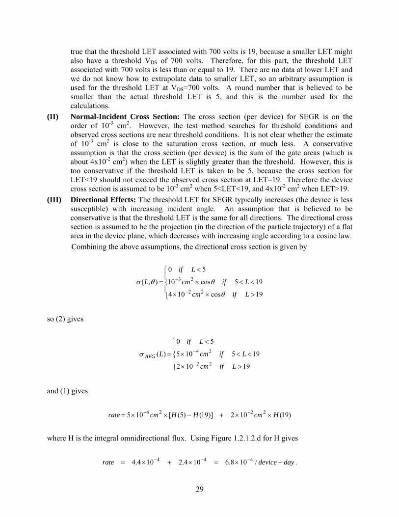
true that the threshold LET associated with 700 volts is 19, because a smaller LET might also have a threshold VDS of 700 volts. Therefore, for this part, the threshold LET associated with 700 volts is less than or equal to 19. There are no data at lower LET and we do not know how to extrapolate data to smaller LET, so an arbitrary assumption is used for the threshold LET at VDS=700 volts. A round number that is believed to be smaller than the actual threshold LET is 5, and this is the number used for the calculations.
(II) Normal-Incident Cross Section: The cross section (per device) for SEGR is on the order of 10-3 cm2. However, the test method searches for threshold conditions and observed cross sections are near threshold conditions. It is not clear whether the estimate of 10-3 cm2 is close to the saturation cross section, or much less. A conservative assumption is that the cross section (per device) is the sum of the gate areas (which is about 4x10⁻² cm2) when the LET is slightly greater than the threshold. However, this is too conservative if the threshold LET is taken to be 5, because the cross section for LET<19 should not exceed the observed cross section at LET=19. Therefore the device cross section is assumed to be 10-3 cm2 when 5<LET<19, and 4x10⁻² cm2 when LET>19.
(III) Directional Effects: The threshold LET for SEGR typically increases (the device is less susceptible) with increasing incident angle. An assumption that is believed to be conservative is that the threshold LET is the same for all directions. The directional cross section is assumed to be the projection (in the direction of the particle trajectory) of a flat area in the device plane, which decreases with increasing angle according to a cosine law. Combining the above assumptions, the directional cross section is given by
⎪⎩
⎪⎨
⎧
>××
<<×
<
=−
−
19cos104
195cos10
50
),(22
23
Lifcm
Lifcm
Lif
L
θ
θθσ
so (2) gives
⎪⎩
⎪⎨
⎧
>×
<<×
<
=−
−
19102
195105
50
)(22
24
Lifcm
Lifcm
Lif
LAVGσ
and (1) gives
)19(102)]19()5([105 2224 HcmHHcmrate ××+−××= −− where H is the integral omnidirectional flux. Using Figure 1.2.1.2.d for H gives
./108.6104.2104.4 444 daydevicerate −×=×+×= −−−
29

3.4.2. Best-Guess Rate The Best-Guess rate is based on the following assumptions:
(I) Normal-Incident Threshold LET: It is assumed that the low point (square) at LET=19 is not representative and that the threshold LET at VDS=700 volts is determined by the lower straight line in the figure. This gives a threshold LET of about 26.5.
(II) Normal-Incident Cross Section: It is assumed that the cross section estimate of 10-3 cm2 (from item (II) in Section 3.4.1) applies to large enough LET so that rates can be calculated from a step function having this saturation value.
(III) Directional Effects: The threshold LET for SEGR typically increases with increasing incident angle. It is assumed that this increase follows an inverse cosine law. The directional cross section is assumed to decrease with increasing angle according to a cosine law.
Combining the above assumptions, the directional cross section is given by
⎪⎩
⎪⎨⎧
>×
<= − θθ
θθσ
cos/5.26cos10
cos/5.260),( 23 Lifcm
LifL
so (1) gives
⎪⎪⎩
⎪⎪⎨
⎧
>⎥⎥⎦
⎤
⎢⎢⎣
⎡⎟⎠⎞
⎜⎝⎛−××
<
= − .5.265.261105
5.260
)( 224 Lif
Lcm
Lif
LAVGσ
3.5. The Alternate Approach An alternative to writing an integration routine to evaluate the integral in Equation (1) is
to use a standard code used for soft error rate calculations. Such a code does not accommodate the assumed directional dependence but can still be used if it is given the appropriate inputs. The inputs are derived as follows. Note that different directional cross sections that produce the same σAVG also produce the same event rate. In particular, the SEGR rate derived from assumptions I, II, and III is the same as the soft error rate for an isotropic device having a cross section curve given by the above equation for σAVG. The latter rate can be approximated using an RPP calculation if the RPPs are cubes. This approximation contains some conservatism because cubes are not exactly isotropic and ion hits near a main diagonal can produce an upset when the LET is less than 26.5. However, this amount of conservatism is less than the uncertainties associated with other assumptions, so the estimate is still regarded as a Best Guess. Using an RPP calculation with the above cross section gives ./104.4 7 daydevicerate −×= −
30

3.6. In Orbit In earth orbit, the flux of GCR will depend on the time spent out of the radiation belts.
Polar orbits will have a larger effective SEE rate from GCR. Prorating the event rate for each radiation type is fine for simple combinations of duty cycle.
3.7. Flares Flares and coronal mass ejections are comprised mostly of protons with a small amount
of heavy ions. The increase in SEGR rate from a flare will depend on shielding present and type of solar event. If a major solar flare occurs, the number of SEGRs accumulated over the duration of the flare is on the order of the number accumulated from one year of solar minimum GCR.
3.8. Rates in Mixed Operational Modes Often mission applications are not as simple as a power device in the off mode for a fixed
period of time. As with environment duty cycle, the rate can be prorated to each time in each operational mode. The most straight forward method is to assume the worst case bias conditions for the off time. If the device is blocking a variable drain-to-source current, then the rate will vary with voltage and therefore time. If this worst case approach yields an unacceptably high risk, the time profile may be broken up piecewise and the analysis above can be used with the total probability being a function of each piece part of the probability (See section 3.9).
3.9. Rates and Probability According to Poisson statistics, the probability of one or more failures during a mission
is Prob = 1 – exp(-rate*duration), (5)
where rate is the event rate and duration is the summation of the total time the device will experience that rate. For very small arguments that are much less than one, the probability will be equal to the argument of (5). 4. Alternate Testing Approaches
Most experimental alternatives to ion testing have the problem of limited range of the radiation type, and, therefore, cannot accurately reflect the SEE characteristics of power devices. These methods can, however, allow for identification of some SEE metrics for devices like gate area and device cross section. Circuit and thermal response can also be extracted from the response of devices using a laser. In this vein, SEE issues can be addressed in a non-beam site setting and reduce cost.
4.1. Laser Testing There has been little testing using a laser with the most relevant testing by [Miller06] in
which SEB is triggered by backside irradiation. Luu also showed that SEB can be induce by backside laser irradiation and that the effect can occur at very low voltages [Luu07]. Peyer showed that SEGR microbreaks could be induced by laser [Peyer07]. Neither study, however, presents a methodology for using the laser as a SEE testing tool.
4.2. Microbeam Microbeams, like lasers, have the ability to control the strike area of the ion, so are very
good in mapping SEE phenomenon in power devices. In [Musseau99], a microbeam is used for just this purpose.
31

4.3. Simulation Currently, simulation is a very good tool for validating general trends of SEE in devices,
but as yet has not been shown to accurately predicted SEE in power devices. A number of papers have been written on this topic, mostly by Titus et al [Titus03], [Liu06], [Titus99], [Titus96] but also by Roubaud et al [Roubaud93], [Dachs95], [Roubaud93]. 5. Design Guidelines
Using a power device in space relies on the correct application of the device and proper assessment of risk. One of the primary challenges for power MOSFET application is the interplay between the device and the local circuit.
5.1. General Derating Since all power devices will experience some form of breakdown, risk free placement of
a power device in a space application relies on reducing the operating conditions to under a critical parameter. This approach is called derating. The success of this derating approach depends mainly on the derating fraction that is used, whether it is 75, 50, or 25%. Often derating is used to envelop part-to-part variation as well as any unknown or exigent events. In short, the cost and time advantage from this approach can streamline a mission assurance effort. But the reduction in device performance may be excessive for many applications.
0 -5 -10 -15 -20Gate-to-source [V]
0
50
100
Dra
in-to
-sou
rce
[V]
SEE for IRHF58160Bromine 36.7MeV-cm2/mg 39.5 um Iodine 59.8MeV-cm2/mg 32.5 um Gold 82.3MeV-cm2/mg 28.4 um
Figure 5.1.a. Typical safe operating data for power MOSFET. Dashed lines represent a 75%
derating. Figure 5.1.a shows a typical set of industry data on a power MOSFET. The most
common form of derating is to specify a fraction of the operating voltage for a prescribed ion. In the figure, for each ion type and LET, a response curve is shown (circles for Gold) with the derated safe operating area (SOA) of 75% in dashed lines. This means that the device in flight
32

should be used at voltages under the derating curve in Figure 5.1.a. Recalling section 2.2.8.1, the range effects of these data should be taken into account in the derating.
Mission assurance approaches like this have several draw backs. The first is that they set an arbitrary level of LET at the compliance level. In most cases, the LET limit is chosen to include all ions under the ion knee (cf. Figure 1.2.1.2.d). Usually, this ion selection ranges from 30 to 40 MeV.cm2/mg. For very short missions, this may be too conservative since the probability of higher LET ions will be much lower. This derating method also assumes that all SEGR/SEB phenomenon are uniform across all power devices. Any data review like Selva03, Mulford02, Boden06, or Coss98 shows that the SEE characteristics vary strongly across device voltage rating, manufacturer, lot, etc. Recalling Figure 1.2.1.2.b, the transition area between the low and high LET response will have a dominant effect on the rate and therefore will be the major consideration in the application of the part. Finally, many exotic and nonlinear SEE occur at very high LETs, so any event that threatens a mission should be derated against these phenomena. For example, microbreaks are much more probable at high LETs and much more damaging for longer missions.
While SEGR depends mainly on the applied bias of the device, all device parameters should be reduced to remove threats from related damage effects (See section 2.2.8.3). Typical derating for transistors is accomplished by multiplying the stress parameter by the appropriate derating factor as shown in Table 5.1.a. Note that the derating factor should be factored into the maximum survival value for the known test data. For example, if a 100V drain-to-source rated device exhibits SEGR at VDS=80V, then resulting operation voltage is 75% of 80V, or 60V. Many of the parameters in Table 5.1.a depend on the electrical and thermal environment in which the device will operate. Therefore, the flight application circuitry and environment should be known to derate safely.
Table 5.1.a. Transistor Derating Requirements
Stress Parameter Derating Factor
Power 0.6 Current 0.75 Voltage (VGS, VDS) 0.75 Junction Temperature 0.8 Voltage slew 0.8 Current slew 0.8
In Table 5.1.a, the current and voltage slew of the device are the change in each
parameter with respect to time and will tend to stress the device. Derating these parameters also is advised since damage from SEE effects can be exacerbated with prompt electrical and thermal stress. Table 5.1.b lists many of the devices that have been tested for space flight and some recommendations for operation. Of course this table cannot be used for mission assurance design since the part-to-part variation alone disallows for a comprehensive derating list. Rather, this table is designed to give a rough estimate of what derating to expect in selecting devices. These data also lead to the observation that no derating approach can be applied uniformly to all SEGR derating since variation is so wide.
33

Table 5.1.b. Transistor Derating Requirements
Device Rating [V]
VDS(SEGR) @VGS=0V
Max VDS w/ 75% derating
Device Rating VDS(SEGR) @VGS=0V
75% derating
2n7299 100 70 52.5 FSF254R 250 250 187.5
FRM140 100 60 45 IRH254 250 225 168.75
INRM58160 100 100 75 IRH7264SE 250 250 187.5
IRF110 100 50 37.5 IXTM35N30 300 67 50.25
IRF120 100 80 60 2N7391SE 400 400 300
IRF130 100 60 45 FLR430 400 72.5 54.375
IRF140 100 50 37.5 IRF310 400 250 187.5
IRF150 100 75 56.25 IRF330 400 200 150
IRFF130 100 82 61.5 IRF340 400 240 180
IRHF7110 100 100 75 IRF350 400 200 150
IRHF7130 100 100 75 IRHM7360 400 125 93.75
IRHF7150 100 60 45 EN469 500 300 225
2n6784 200 100 75 FRM450 500 175 131.25
2n6798 200 140 105 IR7450 500 385 288.75
2n7262 200 155 116.25 IRF430 500 320 240
FRK250 200 80 60 IRF440 500 246 184.5
FRL230D1 200 90 67.5 IRH7450SE 500 500 375
FRM240 200 60 45 IRH8450 500 150 112.5
IR7250 200 125 93.75 TA17466RH 500 500 375
IRF240 200 120 90 IRHY7343 550 575 431.25
IRFF230 200 120 90 APT1004RCN 1000 475 356.25
IRFM250 200 130 97.5 APT10088HV 1000 450 337.5
IRH7250 200 200 150 IRFMG40 1000 450 337.5
IRHF3250 200 100 75 IRHY7G30C 1000 800 600
FRK264R 250 75 56.25 RFP4N100 1000 575 431.25
5.2. Application Specific Derating
As said above, the circuit application greatly affects the SEGR susceptibility of a part. And the likelihood of an SEGR depends directly on the length and environment of the mission. The approach under discussion is to identify the risk acceptable to the part application and identify the part derating commensurate with that risk. This approach avoids a strict methodology as it is up to the personnel composing the test plan and flight design to identify the stressors and other factors that will drive the risk for a particular mission application. It can be seen from this approach that an optimum design is possible for any given set of requirements. As the requirements are restricted, the trade-offs between derating and radiation tolerance drives the design. Also this approach necessarily requires that flight designs be analyzed to determine part stresses per device instance (voltage, current, power, temperature, etc.) in dynamic as well as in steady state applications. The parts stresses will be indexed to the program derating criteria
34

which are summarized in Table 5.1.a. In those cases where the program derating criteria provide insufficient information, or if data is considered as not applicable, additions to margin are necessarily needed. In short, this approach is based on identifying the maximum tolerable risk for mission applications and tailoring the testing and design to reflect that risk.
Figure 5.2.a portrays the main inputs into the failure rate, and therefore the failure probability. The most important fact about this figure is that each input will have a minimum uncertainty that will propagate through the failure probability calculation and will ultimately limit the precision of the risk assessment for any derating approach. The environment is the input about which nothing can be done by the designer or device tester. Regardless of where in the solar system and when during the solar cycle the mission in question travels, the uncertainty in the flux a mission encounters can vary over orders of magnitude. This uncertainty will induce irremovable uncertainly in the failure rate of the device. Recalling section 3.4 as an example, the difference between the best guess and worst case rate calculations, which is mainly due to environmental uncertainty, is at least one order of magnitude.
The “mission application” input of Figure 5.2.a is often laden with a minimum uncertainty. For example, an inductive load power supply, in which power MOSFETs are often used, will change the maximum VDS the device will endure to support a higher load. The range of load that will be required in the mission must be known to capture accurate input data to the failure rate calculation. This effect translates to an uncertainty in the actual circuit and mission operation parameters that will propagate to the rate calculation. Often, the exigent circumstances that can overly stress a device are not readily available to the tester, so careful rendition of the risk versus application may be required. Finally, the SEE test data will have a minimum of uncertainty solely due to part-to-part variation even if the test personnel make every assurance to remove uncertainty in the test data.
The effect of multiple inputs each having a respective uncertainty on the failure rate, and therefore risk assessment, will resulting in the addition of the uncertainties. When several statistical distributions are superimposed in rate calculation, the resulting distribution will be greater than any of the input distributions. The mathematical term for this is convolution. The most relevant property of a convoluted distribution is
∑= 22it σσ
where σt is the standard deviation of the final distribution and σi are the standard deviations of the input distributions. The corollary of this result is that the final distribution (or uncertainty) will be overwhelmingly influenced by the largest input distribution. This implies that the uncertainty of the application specific derating approach will be driven by the most uncertain input to the failure rate calculations. For example, if the uncertainty in the mission radiation environment alone drives a derating that is about the same magnitude as a standard derating in section 5.1, then the effort to perform the application specific derating may not be fruitful.
An example of application specific derating is the following. If a device is required to have a 95% likelihood of success in a 5 year mission, then the design must be such that the resulting probability of a failure must be less than 5%. The user may choose a 1% failure probably to account for the aforementioned environmental uncertainty. The information in section 3.9 can be used to determine the maximum tolerable rate for the desired risk. The rate is the output of section 3.3, so the reverse process of determining the exact device condition that will result in the desired rate is not exact nor are the inputs unique. That is, different operating
35
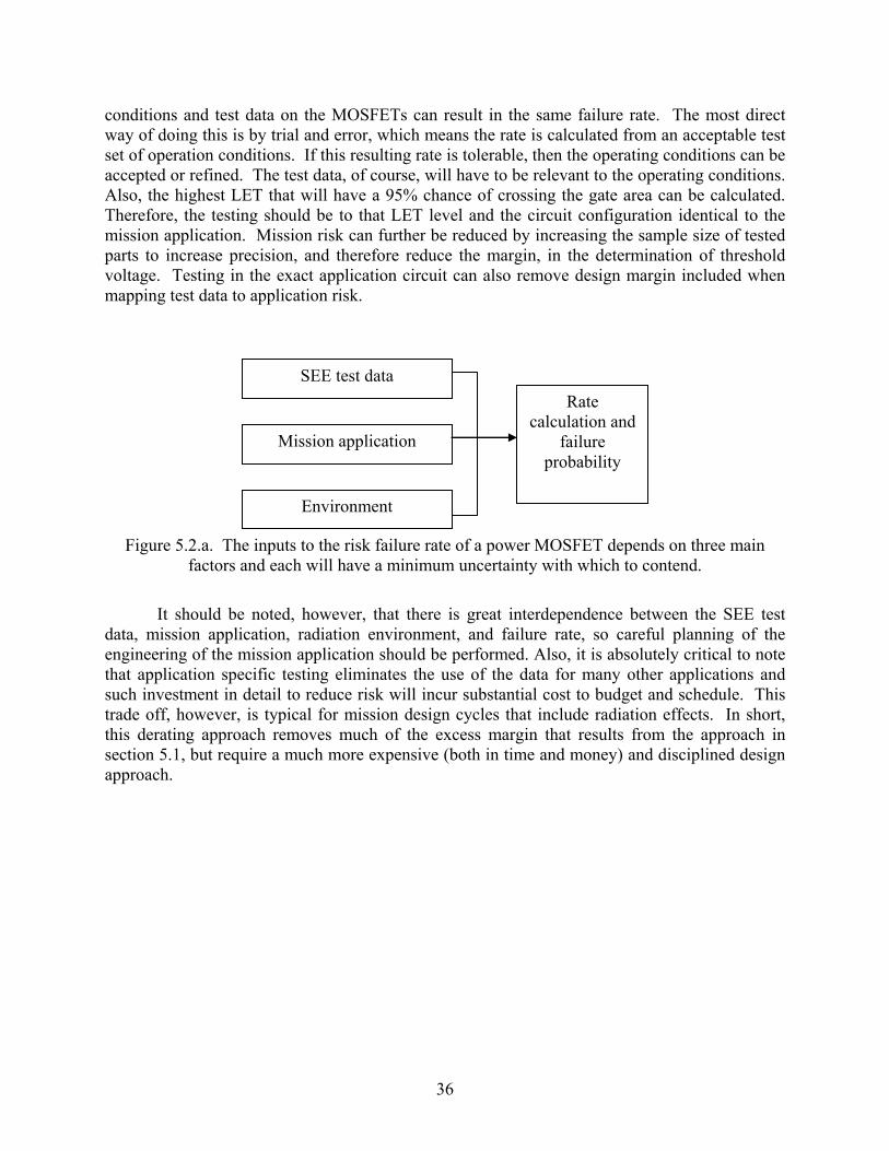
conditions and test data on the MOSFETs can result in the same failure rate. The most direct way of doing this is by trial and error, which means the rate is calculated from an acceptable test set of operation conditions. If this resulting rate is tolerable, then the operating conditions can be accepted or refined. The test data, of course, will have to be relevant to the operating conditions. Also, the highest LET that will have a 95% chance of crossing the gate area can be calculated. Therefore, the testing should be to that LET level and the circuit configuration identical to the mission application. Mission risk can further be reduced by increasing the sample size of tested parts to increase precision, and therefore reduce the margin, in the determination of threshold voltage. Testing in the exact application circuit can also remove design margin included when mapping test data to application risk.
Rate calculation and
failure probability
SEE test data
Environment
Mission application
Figure 5.2.a. The inputs to the risk failure rate of a power MOSFET depends on three main
factors and each will have a minimum uncertainty with which to contend. It should be noted, however, that there is great interdependence between the SEE test
data, mission application, radiation environment, and failure rate, so careful planning of the engineering of the mission application should be performed. Also, it is absolutely critical to note that application specific testing eliminates the use of the data for many other applications and such investment in detail to reduce risk will incur substantial cost to budget and schedule. This trade off, however, is typical for mission design cycles that include radiation effects. In short, this derating approach removes much of the excess margin that results from the approach in section 5.1, but require a much more expensive (both in time and money) and disciplined design approach.
36

References Adell, P.C.; Schrimpf, R.D.; Choi, B.K.; Holman, W.T.; Attwood, J.P.; Cirba, C.R.;
Galloway, K.F.; Total-dose and single-event effects in switching DC/DC power converters, Nuclear Science, IEEE Transactions on, Volume 49, Issue 6, Part 1, Dec. 2002 Page(s):3217 – 3221.
Adophesen J.W., J. L. Barth, and G. B. Gee, “First observation of proton induced power MOSFET burnout in space: The CRUX experiment on APEX,” IEEE Trans. Nucl. Sci., vol. 43, pp. 2921–2926, Dec. 1996.
Albadri, A.M.; Schrimpf, R.D.; Walker, D.G.; Mahajan, S.V.; Coupled electro-thermal Simulations of single event burnout in power diodes, Nuclear Science, IEEE Transactions on, Volume 52, Issue 6, Part 1, Dec. 2005 Page(s):2194 – 2199.
Allenspach M., C. Dachs, G. H. Johnson, R. D. Schrimpf, E. Lorfevre, J. M. Palau, J. R. Brews, K. F. Galloway, J. L. Titus, and C. F. Wheatley, “SEGR and SEB in n-channel power MOSFETs,” IEEE Trans. Nucl. Sci., vol. 43, pp. 2927–2931, 1996.
Allenspach M., I. Mouret, J. L. Titus, C. F. Wheatley, Jr., R. L. Pease, J. R. Brews, R. D. Schrimpf, and K. F. Galloway, “Single-event gate rupture in power MOSFETs: Prediction of breakdown biases and evaluation of oxide thickness dependence,” IEEE Trans. Nucl. Sci., vol. 42, pp. 1922–1927, Dec. 1995.
Allenspach M., J. R. Brews, I. Mouret, R. D. Schrimpt, and K. F. Galloway, “Evaluation of SEGR threshold in power MOSFETs,” IEEE Trans. Nucl. Sci., vol. 41, pp. 2160–2166, Dec. 1994.
Barth, J.L.; Adolphsen, J.W.; Gee, G.B.; Single event effects on commercial SRAMs and power MOSFETs: final results of the CRUX flight experiment on APEX, Radiation Effects Data Workshop, 1998. IEEE, 24 July 1998 Page(s):1 – 10.
Becker, H.; Chavez, R.; Scheick, L.; Selva, L.; Effects of Radiation on Commercial Power Devices, Radiation Effects Data Workshop, 2006 IEEE, July 2006 Page(s):57 – 61.
Blandford T. J., Jr., A. E. Waskiewicz, and J. C. Pickel, “Cosmic ray induced permanent damage in MNOS EAROMs,” IEEE Trans. Nucl. Sci., vol. 31, pp. 1568–1570, Dec. 1984.
Boden, M.; Milt Boden; Liu, S.; Sanchez, E.; Titus, J.L.; Evaluation of Worst-Case Test Conditions for SEE on Power DMOSFETs, Radiation Effects Data Workshop, 2006 IEEE, July 2006 Page(s):165 – 171.
Boruta N., G. K. Lum, H. O’Donnell, L. Robinette, M. R. Shaneyfelt, and J. R. Schwank, “A new physics-based model for understanding single-event gate rupture in linear devices,” IEEE Trans. Nucl. Sci., vol. 48, pp. 1917–1924, Dec. 2001.
Brews J. R., M. Allenspach, R. D. Schrimpf, and K. F. Galloway, “A conceptual model of single-event gate-rupture in power MOSFETs,” IEEE Trans. Nucl. Sci., vol. 40, pp. 1959–1966, Dec. 1993.
Brucker G. J., P. Messel, D. Oberg, J.Wert, and T. Criswell, “SEU sensitivity of power converters with MOSFETS in space,” IEEE Trans. Nucl. Sci., vol. 34, pp. 1792–1795, 1987.
Calvel P., C. Peyrotte, A. Baiget, and E. G. Stassinopoulos, “Comparison of experimental measurements of power MOSFET SEB’s in dynamic and static modes,” IEEE Trans. Nucl. Sci., vol. 38, pp. 1310–1314, 1991.
37
Coss, J.R.; Swift, G.M.; Selva, L.E.; Titus, J.L.; Normand, E.; Oberg, D.L.; Wert, J.L.; Compendium of single event failures in power MOSFETs, Radiation Effects Data Workshop, 1998. IEEE, 24 July 1998 Page(s):15 – 38.
Dachs C., F. Rouband, J.-M. Palau, G. Bruguier, J. Gasiot, and P. Tastet, “Evidence of the ion’s impact position effect on SEB in n-channel power MOSFETs,” IEEE Trans. Nucl. Sci., vol. 41, pp. 2167–2171, 1994.
Dachs, C.; Roubaud, F.; Palau, J.-M.; Bruguier, G.; Gasiot, J.; Tastet, P.; Calvett, M.-C.; Calvel, P.; Simulation aided hardening of N-channel power MOSFETs to prevent single event burnout, Nuclear Science, IEEE Transactions on, Volume 42, Issue 6, Part 1, Dec. 1995 Page(s):1935 – 1939.
Dachs, C.; Roubaud, F.; Palau, J.-M.; Bruguier, G.; Gasiot, J.; Tastet, P.; Evidence of the ion's impact position effect on SEB in N-channel power MOSFETs, Nuclear Science, IEEE Transactions on, Volume 41, Issue 6, Part 1, Dec 1994 Page(s):2167 – 2171.
Fischer T. A., “Heavy-ion-induced gate rupture in power MOSFETS,” IEEE Trans. Nucl. Sci., vol. 34, pp. 1786–1791, Dec. 1987.
Gillberg, J.E.; Burton, D.I.; Titus, J.L.; Wheatley, C.F.; Hubbard, N.; Responses of radiation-hardened power MOSFETs to neutrons, Radiation Effects Data Workshop, 2001 IEEE, 16-20 July 2001 Page(s):160 – 166.
Gillberg, J.E.; Titus, J.L.; Hubbard, N.; Burton, D.I.; Wheatley, C.F.; Updated responses of devices from the FSG and FSP radiation-hardened power MOSFET families to 1-MeV equivalent neutrons, Radiation Effects Data Workshop, 2002 IEEE, 15-19 July 2002 Page(s):138 – 144.
Hohl J. H. and G. H. Johnson, “Features of the triggering mechanism for single event burnout of power MOSFETs,” IEEE Trans. Nucl. Sci., vol. 35, pp. 2260–2266, 1989.
Hohl J. H. and K. F. Galloway, “Analytical model for single event burnout of power MOSFETs,” IEEE Trans. Nucl. Sci., vol. 34, pp. 1275–1230, 1987.
Huang S., G. A. J. Amaratunga, and F. Udrea, “Analysis of SEB and SEGR in super-junction MOSFETs,” IEEE Trans. Nucl. Sci., vol. 47, pp. 2640–2647, Dec. 2000.
Johnson G. H., K. F. Galloway, R. D. Schrimpf, J. L. Titus, C. F. Wheatley, M. Allenspach, and C. Dachs, “A physical interpretation for the single-event-gate-rupture cross-section of n-channel power MOSFETs,” IEEE Trans. Nucl. Sci., vol. 43, pp. 2932–2937, 1996.
Johnson G. H., R. D. Schrimpf, K. F. Galloway, and R. Koga, “Temperature dependence of single-event burnout in n-channel power MOSFETs,” IEEE Trans. Nucl. Sci., vol. 39, pp. 1605–1612, 1992.
Johnson, G.H.; Palau, J.M.; Dachs, C.; Galloway, K.F.; Schrimpf, R.D.; A review of the techniques used for modeling single-event effects in power MOSFETs, Nuclear Science, IEEE Transactions on, Volume 43, Issue 2, Part 1, April 1996 Page(s):546 – 560.
Koga, R.; Single-event effect ground test issues, Nuclear Science, IEEE Transactions on, Volume 43, Issue 2, Part 1, April 1996 Page(s):661 – 670.
Kuboyama S., S. Matsuda, T. Kanno, and T. Ishii, “Mechanism for single-event burnout of power MOSFET’s and its characterization technique,” IEEE Trans. Nucl. Sci., vol. 39, pp. 1698–1703, Dec. 1992.
38

Lehman, J.; Yui, C.; Rax, B.G.; Miyahira, T.F.; Wiedeman, M.; Schrock, P.; Swift, G.M.; Johnston, A.H.; Kayali, S.; Low dose failures of hardened DC-DC power converters, Radiation Effects Data Workshop, 2002 IEEE, 15-19 July 2002 Page(s):109 – 114.
Liu, S.; Boden, M.; Girdhar, D. A.; Titus, J. L.; Single-Event Burnout and Avalanche Characteristics of Power DMOSFETs, Nuclear Science, IEEE Transactions on, Volume 53, Issue 6, Part 1, Dec. 2006 Page(s):3379 – 3385.
Lorfevre, E.; Sudre, C.; Dachs, C.; Detcheverry, C.; Palau, J.-M.; Gasiot, J.; Calvet, M.-C.; Garnier, J.; Ecoffet, R.; SEB occurrence in a VIP: influence of the epi-substrate junction, Radiation and Its Effects on Components and Systems, 1997. RADECS 97. Fourth European Conference on, 15-19 Sept. 1997 Page(s):557 – 560.
Lum, G.K.; Boruta, N.; Baker, J.M.; Robinette, L.; Shaneyfelt, M.R.; Schwank, J.R.; Dodd, P.E.; Felix, J.A.;, New experimental findings for single-event gate rupture in MOS capacitors and linear devices, Nuclear Science, IEEE Transactions on, Volume 51, Issue 6, Part 2, Dec. 2004 Page(s):3263 – 3269.
Lum, G.K.; O'Donnell, H.; Boruta, N.; The impact of single event gate rupture in linear devices, Nuclear Science, IEEE Transactions on, Volume 47, Issue 6, Part 3, Dec. 2000 Page(s):2373 – 2379.
Luu A., F. Miller, P. Poirot, P. Austin, R. Gaillard, N. Buard, T. Carrière, M. Bafleur, G. Sarrabayrouse, “SEB characterisation of commercial power MOSFETs with backside laser and heavy ions of different ranges,” Presented at the 2007 Radiation and Its Effects on Electronics Conference, Deauville.
Martin R. C., N. M. Ghoniem, Y. Song, and J. S. Cable, “The size effect of ion charge tracks on single event multiple-bit upset,” IEEE Trans. Nucl. Sci., vol. 34, pp. 1305–1309, 1987.
McDonald P. T., B. G. Henson, and W. J. Stapor, “Destructive failure of OP470/OP471 operational amplifiers due to breakdown of gate oxides during space radiation performance qualification,” in HEART/GOMAC Conf. Rec., vol. 25, 2000, pp. 336–339.
Milgram A. A., “Ion-induced electrical breakdown in metal-oxide-silicon capacitors,” J. Appl. Phys., vol. 67, no. 3, pp. 1461–1470, 1990.
Miller, F.; Luu, A.; Prud'homme, F.; Poirot, P.; Gaillard, R.; Buard, N.; Carrire, T.; Characterization of Single-Event Burnout in Power MOSFET Using Backside Laser Testing, Nuclear Science, IEEE Transactions on, Volume 53, Issue 6, Part 1, Dec. 2006 Page(s):3145 – 3152.
Mohan, N., Power electronics: converters, applications, and design, John Wiley & Sons, 2003.
Mouret I., M. Allenspach, R. D. Schrimpf, J. R. Brews, and K. F. Galloway, “Temperature and angular dependence of substrate response in SEGR,” IEEE Trans. Nucl. Sci., vol. 41, pp. 2216–2221, Dec. 1994.
Mouret, I.; Calvel, P.; Allenspach, M.; Titus, J.L.; Wheatley, C.F.; LaBel, K.A.; Calvet, M.-C.; Schrimpf, R.D.; Galloway, K.F.; Measurement of a cross-section for single-event gate rupture in power MOSFETs, Electron Device Letters, IEEE, Volume 17, Issue 4, April 1996 Page(s):163 – 165.
39

Mulford, S.G.; Brown, D.N.; McMaster, A.L.; Nuclear dose rate, total dose and neutron radiation testing of COTS devices, Radiation Effects Data Workshop, 2002 IEEE, 15-19 July 2002 Page(s):145 – 151.
Musseau, O.; Torres, A.; Campbell, A.B.; Knudson, A.R.; Buchner, S.; Fischer, B.; Schlogl, M.; Briand, P.; Medium-energy heavy-ion single-event-burnout imaging of power MOSFETs, Nuclear Science, IEEE Transactions on, Volume 46, Issue 6, Dec. 1999 Page(s):1415 – 1420.
Nguyen, D.N.; Guertin, S.M.; Swift, G.M.; Johnston, A.H.; Radiation effects on advanced flash memories, , Nuclear Science, IEEE Transactions on, Volume 46, Issue 6, Dec. 1999 Page(s):1744 – 1750.
Nichols D. K., J. R. Coss, and K. P. McCarty, “Single event gate rupture in commercial power MOSFETs,” in Proc. 2nd Eur. Conf. Radiation and Its Effects on Components and Systems, Saint-Malo, France, Sept. 13–16, 1993, pp. 462–467.
Nichols, D.K.; Coss, J.R.; Miyahira, T.; Titus, J.; Oberg, D.; Wert, J.; Majewski, P.; Lintz, J.; Update of single event failure in power MOSFETs, Radiation Effects Data Workshop, 1996., IEEE, 19 July 1996 Page(s):67 – 72.
Nichols, D.K.; McCarty, K.P.; Coss, J.R.; Waskiewicz, A.; Groninger, J.; Oberg, D.; Wert, J.; Majewski, P.; Koga, R.; Observations of single event failure in power MOSFETs, Radiation Effects Data Workshop, 1994 IEEE, 20 July 1994 Page(s):41 – 54.
Normand E., J. L,Wert, D. L. Oberg, P. P. Majewski, and P. Voss, “Neutron- induced single event burnout in high voltage electronics,” IEEE Trans. on Nucl. Sci., vol. 44, pp. 2358–2366, Dec. 1997.
O’Bryan M. V., K. A. LaBel, R. A. Reed, J. W. Howard, J. L. Barth, C. M. Seidleck, P. W. Marshould, C. J. Marshould, H. S. Kim, D. K. Hawkins, M. A. Carts, and K. E. Forslund, “Recent radiation damage and single event effects results for microelectronics,” in IEEE Radiation Effects Data Workshop Rec., 1999, pp. 1–14.
Oberg D. L. and J. L.Wert, “First nondestructive measurements of power MOSFET single event burnout cross sections,” IEEE Trans. Nucl. Sci., vol. 34, pp. 1736–1741, 1987.
Oberg D. L., J. L. Wert, E. Normand, P. P. Majewski, and S. A. Wender, “First observations of power MOSFET burnout with high energy neutrons,” IEEE Trans. Nucl. Sci., vol. 43, pp. 2913–2920, 1996.
Peyre, D. Ch. Binois, R. Mangeret, T. Bouche, F. Bezerra, R. Ecoffet and E. Lorfèvre, “SEGR on power MOSFETs: a cumulative phenomena,” Presented at the 2006 Radiation and Its Effects on Electronics Conference, Athens.
Peyre D., Ch. Binois, R. Mangeret, G. Salvaterra, M. Beaumel, F. Pontoni, T. Bouchet, L. Pater, F. Bezerra, R. Ecoffet, E. Lorfèvre, F. Sturesson, G. Berger, J.C. Foy, B. Piquet, “SEGR study on Power MOSFETs: follow-on,” Presented at the 2007 Radiation and Its Effects on Electronics Conference, Deauville.
Pickel J. C. and A. E. Waskiewicz, “Heavy ion induced permanent damage in MNOS gate insulators,” IEEE Trans. Nucl. Sci., vol. 32, pp. 4176–4179, Dec. 1985.
Pickel J. C. and T. J. Blandford, Jr., “Cosmic ray induced errors in MOS devices,” IEEE Trans. Nucl. Sci., vol. 27, pp. 1005–1015, Apr. 1980.
40

Reed R. A., J. Kinnison, J. C. Pickel, S. Buchner, P. W. Marshould, S. Kniffin, and K. A. LaBel, “Single-event effects ground testing and on-orbit rate prediction methods: The past, present and future,” IEEE Trans. Nucl. Sci., vol. 50, pp. 622–634, June 2003.
Richter A. K. and I. Arimura, “Simulation of heavy charged particle tracks using focused laser beams,” IEEE Trans. Nucl. Sci., vol. 34, pp. 1234–1239, 1987.
Roubaud, F.; Dachs, C.; Palau, J.-M.; Gasiot, J.; Tastet, P.; Experimental and 2D simulation study of the single-event burnout in N-channel power MOSFETs, Nuclear Science, IEEE Transactions on, Volume 40, Issue 6, Part 1-2, Dec 1993 Page(s):1952 – 1958.
Roubaud, F.; Dachs, C.; Palau, J.-M.; Gasiot, J.; Tastet, P.; Use of 2D simulations to study parameters influence on SEB occurrence in n-channel MOSFETs, Radiation and its Effects on Components and Systems, 1993.,RADECS 93., Second European Conference on, 13-16 Sept. 1993 Page(s):446 – 451.
Savage M. W., D. I. Burton, C. F. Wheatley, J. L. Titus, and J. E. Goldberg, “An improved stripe-cell SEGR hardened power MOSFET technology,” IEEE Trans. Nucl. Sci., vol. 48, pp. 1872–1878, Dec. 2001.
Scheick, L., Selva, L,. Edmonds, L., Effect of dose history on SEE properties of power MOSFETS, To be published.
Selva L. E., G. M. Swift,W. A. Taylor, and L. D. Edmonds, “On the role of energy deposition in triggering SEGR in power MOSFETs,” IEEE Trans. Nucl. Sci., vol. 46, pp. 1403–1409, 1999.
Selva, L.E.; Scheick, L.Z.; McClure, S.; Miyahira, T.; Guertin, S.M.; Shah, S.K.; Edmonds, L.D.; Patterson, J.D.; Catastrophic SEE in high-voltage power MOSFETs, Radiation Effects Data Workshop, 2003. IEEE, 21-25 July 2003 Page(s):113 – 120.
Sexton F. W., “Microbeam studies of single event effects,” IEEE Trans. Nucl. Sci., vol. 43, pp. 687–695, Apr. 1996.
Sexton F.W., D. M. Fleetwood, M. R. Shaneyfelt, P. E. Dodd, G. L. Hash, K. S. Krisch, M. L. Green, B. E. Weir, and P. J. Silverman, “Precursor ion damage and angular dependence of single event gate rupture in thin oxides,” IEEE Trans. Nucl. Sci., vol. 45, pp. 2509–2518, Dec. 1998.
Sexton, F.W.; Destructive single-event effects in semiconductor devices and ICs, Nuclear Science, IEEE Transactions on, Volume 50, Issue 3, Part 3, June 2003 Page(s):603 – 621.
Sexton, F.W.; Fleetwood, D.M.; Shaneyfelt, M.R.; Dodd, P.E.; Hash, G.L.; Schanwald, L.P.; Loemker, R.A.; Krisch, K.S.; Green, M.L.; Weir, B.E.; Silverman, P.J.; Precursor ion damage and angular dependence of single event gate rupture in thin oxides, Nuclear Science, IEEE Transactions on, Volume 45, Issue 6, Part 1, Dec. 1998 Page(s):2509 – 2518.
Sexton, F.W.; Fleetwood, D.M.; Shaneyfelt, M.R.; Dodd, P.E.; Hash, G.L.; Single event gate rupture in thin gate oxides, Nuclear Science, IEEE Transactions on, Volume 44, Issue 6, Part 1, Dec. 1997 Page(s):2345 – 2352.
Srour, J. R.; Palko, J. W.; A Framework for Understanding Displacement Damage Mechanisms in Irradiated Silicon Devices. Nuclear Science, IEEE Transactions on, Volume 53, Issue 6, Part 1, Dec. 2006 Page(s):3610 – 3620.
41

Srour, J.R.; Marshould, C.J.; Marshould, P.W.; Review of displacement damage effects in silicon devices, , Nuclear Science, IEEE Transactions on, Volume 50, Issue 3, Part 3, June 2003 Page(s):653 – 670.
Stassinopoulos E. G., G. J. Brucker, P. Calvel, A. Baiget, C. Peyrotte, and R. Gaillard, “Charge generation by heavy ions in power MOSFET’s, burnout space predictions, and dynamic SEB sensitivity,” IEEE Trans. Nucl. Sci., vol. 39, pp. 1704–1711, 1992.
Swift, G.; Katz, R.; An experimental survey of heavy ion induced dielectric rupture in Actel Field Programmable Gate Arrays (FPGAs), Nuclear Science, IEEE Transactions on, Volume 43, Issue 3, Part 1, June 1996 Page(s):967 – 972.
Sze S. M., Physics of Semiconductor Devices. New York:Wiley, 1981, pp. 402–407. Taur, Y: Ning, T: Fundamentals of Modern VLSI Devices, Cmpbridge, 2001. Titus J. L., C. F. W heatley, M. Allenspach, R. D. Schrimpf, D. I. Burton, J. R. Brews,
K. F. Galloway, and R. L. Pease, “Influence of ion beam energy on SEGR failure thresholds of vertical power MOSFETs,” IEEE Trans. Nucl. Sci., vol. 43, pp. 2938–2943, 1996.
Titus J. L., C. F. Wheatley, D. I. Burton, I. Mouret, M. Allenspach, J. Brews, R. Schrimpf, K. Galloway, and R. L. Pease, “Impact of oxide thickness on SEGR failure in vertical power MOSFETs; Development of a semi-empirical expression,” IEEE Trans. Nucl. Sci., vol. 42, pp. 1928–1934, Dec. 1995.
Titus J. L., C. F. Wheatley, J. E. Gillberg, and D. I. Burton, “A study of ion energy and its effects upon and SEGR-hardened stripe-cell MOSFET technology,” IEEE Trans. Nucl. Sci., vol. 48, pp. 1879–1884, Dec. 2001. [81] J. L. Titus and C. F. Wheatley, “Proton-induced dielectric breakdown of power MOSFETs,” IEEE Trans. Nucl. Sci, vol. 45, pp. 2891–2897, Dec. 1998.
Titus J. L., C. F. Wheatley, K. M. Van Tyne, J. F. Krieg, D. I. Burton, and A. B. Campbell, “Effect of ion energy upon dielectric breakdown of the capacitor response,” IEEE Trans. Nucl. Sci., vol. 45, pp. 2492–2499, 1998.
Titus J. L., G. H. Johnson, R. D. Schrimpf, and K. F. Galloway, “Single event burnout of power bipolar junction transistors,” IEEE Trans. Nucl. Sci., vol. 38, pp. 1315–1322, 1991.
Titus J. L., L. S. Jamiolkowski, and C. F. Wheatley, “Development of cosmic ray hardened power MOSFETs,” IEEE Trans. Nucl. Sci., vol. 36, pp. 2375–2382, 1989.
Titus, J.L.; Wheatley, C.F.; Allenspach, M.; Schrimpf, R.D.; Burton, D.I.; Brews, J.R.; Galloway, K.F.; Pease, R.L.; “Influence of ion beam energy on SEGR failure thresholds of vertical power MOSFETs,” Nuclear Science, IEEE Transactions on, Volume 43, Issue 6, Part 1, Dec. 1996 Page(s):2938 – 2943.
Titus, J.L.; Wheatley, C.F.; Wheatley, T.H.; Levinson, W.A.; Burton, D.I.; Barth, J.L.; Reed, R.A.; LaBel, K.A.; Howard, J.W.; van Tyne, K.M.; “Prediction of early lethal SEGR failures of VDMOSFETs for commercial space systems,” Nuclear Science, IEEE Transactions on, Volume 46, Issue 6, Dec. 1999 Page(s):1640 – 1651.
Titus, J.L.; Yen-Sheng Su; Savage, M.W.; Mickevicius, R.V.; Wheatley, C.F.; Simulation study of single-event gate rupture using radiation-hardened stripe cell power MOSFET structures, Nuclear Science, IEEE Transactions on, Volume 50, Issue 6, Part 1, Dec. 2003 Page(s):2256 – 2264.
42

43
Titus J.L.et al., “Proton-Induced Dielectric Breakdown of Power MOSFETs”, IEEE Trans. Nucl. Science, Vol.45, No.6, December 1998, p.2891.
Waskiewicz A. E. and J. W. Groninger, “Burnout thresholds and cross sections of power MOSFET transistors with heavy ions,”, Rockwell Int. Rep., Nov. 1988.
Waskiewicz A. E., J. W. Groniger, V. H. Strahan, and D. M. Long, “Burnout of power MOS transistors with heavy ions of Californium- 252,” IEEE Trans. Nucl. Sci., vol. 33, pp. 1710–1713, 1986.
Wheatley, T.H., Wheatley, C.F., Titus, J.L., “Early lethal SEGR failures of VDMOSFETs considering nonuniformity in the rad-hard device distribution,” IEEE Trans. Nucl. Sci., vol. 48, pp. 2217 - 2221, Dec. 2001.
Wheatley C. F., J. L. Titus, and D. I. Burton, “Single-event gate rupture in vertical power MOSFETs; An original empirical expression,” IEEE Trans. Nucl. Sci., vol. 41, pp. 2152–2159, Dec. 1994.
Wheatley C. F., J. L. Titus, D. I. Burton, and D. R. Carley, “SEGR response of a radiaton-hardened power MOSFET technology,” IEEE Trans. Nucl. Sci., vol. 43, pp. 2944–2951, Dec. 1996.
Wheatley, C.F.; Titus, J.L.; Burton, D.I.; “Single-event gate rupture in vertical power MOSFETs; an original empirical expression,” Nuclear Science, IEEE Transactions on, Volume 41, Issue 6, Part 1, Dec 1994 Page(s):2152 – 2159.
Wrobe l T. F., “On heavy ion induced hard-errors in dielectric structures,” IEEE Trans. Nucl. Sci., vol. 34, pp. 1262–1268, Dec. 1987.
Wrobel T. F., F. N. Coppage, G. L. Hash, and A. Smith, “Current induced avalanche in epitaxial structures,” IEEE Trans. Nucl. Sci., vol. 32, pp. 3991–3995, Dec. 1985.
REPORT DOCUMENTATION PAGE Form Approved OMB No. 0704-0188
The public reporting burden for this collection of information is estimated to average 1 hour per response, including the time for reviewing instructions, searching existing data sources, gathering and maintaining the data needed, and completing and reviewing the collection of information. Send comments regarding this burden estimate or any other aspect of this collection of information, including suggestions for reducing this burden, to Department of Defense, Washington Headquarters Services, Directorate for Information Operations and Reports (0704-0188), 1215 Jefferson Davis Highway, Suite 1204, Arlington, VA 22202-4302. Respondents should be aware that notwithstanding any other provision of law, no person shall be subject to any penalty for failing to comply with a collection of information if it does not display a currently valid OMB control number. PLEASE DO NOT RETURN YOUR FORM TO THE ABOVE ADDRESS.1. REPORT DATE (DD-MM-YYYY) 12-17-2007
2. REPORT TYPE JPL Publication
3. DATES COVERED (From - To) N/A
5a. CONTRACT NUMBER NAS7-03001 5b. GRANT NUMBER
4. TITLE AND SUBTITLE Testing Guideline for Single Event Gate Rupture (SEGR) of Power MOSFETs
5c. PROGRAM ELEMENT NUMBER 5d. PROJECT NUMBER 102197 5e. TASK NUMBER 3.23.5
6. AUTHOR(S) Leif Scheick
5f. WORK UNIT NUMBER
7. PERFORMING ORGANIZATION NAME(S) AND ADDRESS(ES) Jet Propulsion Laboratory California Institute of Technology 4800 Oak Grove Drive Pasadena, CA 91009
8. PERFORMING ORGANIZATION REPORT NUMBER JPL Publication 08-10
10. SPONSORING/MONITOR'S ACRONYM(S) NASA NEPP
9. SPONSORING/MONITORING AGENCY NAME(S) AND ADDRESS(ES) National Aeronautics and Space Administration Washington, DC 20546-0001 11. SPONSORING/MONITORING
REPORT NUMBER 0
12. DISTRIBUTION/AVAILABILITY STATEMENT Unclassified—Unlimited Subject Category 76 Solid Sate Physics Availability: NASA CASI (301) 621-0390 Distribution: Nonstandard 13. SUPPLEMENTARY NOTES
14. ABSTRACT The use of power MOSFETs in space can be challenging due to the ubiquitous and diverse nature of radiation that these devices encounter. Radiation can degrade the electrical properties of the device, which depending on the type and severity of the radiation can render the device non-functional. Radiation testing provides a method for characterizing, or at least highlighting, radiation susceptible devices planned for use in space missions. The purpose of this document is two-fold. First, the document lists and discusses many of the issues important to understand when testing power MOSFETs. Second, the recommended approach for using radiation test data to define the device application requirements is presented. These include SEE rate calculation, data analysis, and derating guidelines.
15. SUBJECT TERMS VDMOSFET, Power MOSFET, SEE, SEGR, SEG, Single Event
16. SECURITY CLASSIFICATION OF: 19a. NAME OF RESPONSIBLE PERSON STI Help Desk at [email protected] a. REPORT
U b. ABSTRACT U
c. THIS PAGE U
17. LIMITATION OF ABSTRACT UU
18. NUMBER OF PAGES 49 19b. TELEPHONE NUMBER (Include area code)
(301) 621-0390
JPL 2659 R 10 / 03 W Standard Form 298 (Rev. 8-98) Prescribed by ANSI Std. Z39-18