technology assessment and feasibility study of high-...
TRANSCRIPT

1
Technology Assessment and Feasibility Study of High-
Throughput Single Cell Force Spectroscopy
By
He Cheng
B.E. Bioengineering
Nanyang Technological University, 2009
SUBMITTED TO THE DEPARTMENT OF MATERIALS SCIENCE AND
ENGINEERING IN PARTIAL FULTILLMENT OF THE REQUIREMENTS FOR THE
DEGREE OF
MASTER OF ENGEEIRING IN MATERIALS SCIENCE AND ENGINEERING
AT THE
MASSACHUSETTS INSTITUTE OF TECHNOLOGY
© 2010 Massachusetts Institute of Technology
All rights reserved.
Signature of Author: …………………………………………………………………….
Department of Materials Science and Engineering
Certified by: ……………………………………………………………………………..
Christine Ortiz,
Thesis Supervisor
Professor of Materials Science and Engineering
Accepted by: …………………………………………………………………………….
Christopher Schuh
Chair,
Departmental Committee on Graduate Students

2
Technology Assessment and Feasibility Study of High-
Throughput Single Cell Force Spectroscopy
By
He Cheng
B.E. Bioengineering
Nanyang Technological University, 2009
SUBMITTED TO THE DEPARTMENT OF MATERIALS SCIENCE AND
ENGINEERING IN PARTIAL FULTILLMENT OF THE REQUIREMENTS
FOR THE DEGREE OF
MASTER OF ENGEEIRING IN MATERIALS SCIENCE AND
ENGINEERING
AT THE
MASSACHUSETTS INSTITUTE OF TECHNOLOGY
SEPTEMBER 2010

3
Abstract
In the last decade, the field of single cell mechanics has emerged with the
development of high resolution experimental and computational methods, providing
significant amount of information about individual cells instead of the averaged
characteristics provided by classical assays from large populations of cells. These
single cell mechanical properties correlate closely with the intracellular organelle
arrangement and organization, which are determined by load bearing cytoskeleton
network comprised of biommolecules.
This thesis will assess the feasibility of a high throughput single cell force
spectroscopy using an atomic force microscopy (AFM)-based platform. A
conventional AFM set-up employs a single cantilever probe for force measurement by
using laser to detect the deflection of the cantilever structure, and usually can only
handle one cell at a time. To improve the throughput of the device, a modified scheme
to make use of cantilever based array is proposed and studied in this project. In
addition, to complement the use of AFM array, a novel cell chip design is also
presented for the fine positioning of cells in coordination with AFM cantilevers. The
advantages and challenges of the system are analyzed too. To assess the feasibility of
developing this technology, the commercialization possibility is discussed with
intellectual property research, market analysis, cost modelling and supply chain
positioning. Conclusion about this technology and its market prospect is drawn at the
end of the thesis.

4
Acknowledgements
My sincerest gratitude goes to my thesis supervisor, Prof. Christine Ortiz from the
Department of Materials Science and Engineering, who has offered invaluable advice
on the evolution of this thesis project.
Also, I would like to thank Professor Eugene Fitzgerald for coordinating the Master of
Engineering program. I am grateful to the faculty and staff of the Department of
Materials Science and Engineering at Massachusetts Institute of Technology as they
have made my studies challenging and enjoyable.
I would also like to thank everyone to my fellow SMA dear friends and student
colleagues for their company through the memorable moments we shared together. I
also want to thank the staff from SMA for their warm help and interesting activities.
I thank Singapore-MIT Alliance for financial support and my family and friends for
their love and encouragement.

5
Table of Contents
Abstract 3
Acknowledgement 4
Table of Contents 5
List of Figures 7
Chapter 1 Introduction 8
1.1 Overview and Scope 8
1.2 Single Cell Mechanics 9
1.2.1 Single Cell Mechanics for Cell Characterization 9
1.2.2 Single Cell Mechanics for Diseases Indication 10
1.2.3 Modelling of Single Cell Mechanics 12
1.3 Tools for Mechanical Properties Measurement 15
1.3.1 Mechanical Probing by AFM 17
Chapter 2 High Throughput Single Cell Measurement Technology 21
2.1 High-throughput AFM system 24
2.1.1 Millipede Array 25
2.1.2 Individually Controlled Cantilever with Sensor and Actuator 27
2.1.3 Cantilever Array Design 31
2.2 Cell Chip 34
2.2.1 Cell Chip Design 40
2.3 Integration and Control 45

6
2.4 Challenge and Other Applications 48
2.4.1 Beyond Biology 50
Chapter 3 Commercialization 52
3.1 Intellectual Property 52
3.2 Market 53
3.3 Case Study 55
3.4 Business Strategy 56
3.4.1 Supply Chain Positioning 57
3.4.2 Cost Modelling 59
3.4.3 Utility and Feasibility Analysis 62
Conclusion 63
References 65
Appendix A 77
Appendix B 81
7
List of Figures
Figure 1. Single cell mechanics publications per year 8
Figure 2. Tensegrity model of cell mechanics 14
Figure 3. Tools for single cell mechanics measurement 16
Figure 4. Principle of AFM operation 18
Figure 5. Complex modulus measurement by AFM indentation 19
Figure 6. AFM measurement directly correlates with cytoskeleton 20
Figure 7. Non-Gaussian distribution of cell population with different deformability 22
Figure 8. Averaged property measured with a population of cells 23
Figure 9. Concept of proposed high-throughput single cell force measurement device 24
Figure 10. Schematic drawing showing Millipede concept 26
Figure 11. Schematic drawing shows cantilever with integrated sensor and actuator 29
Figure 12. Modified scheme for integration of sensing and actuation 30
Figure 5. Cantilever array fabrication process 33
Figure 6. Mechanical fluidic positioning of cells 35
Figure 7. Chemical compositions of SAM layer, X is the end group 36
Figure 8. General approach for micro contact printing 37
Figure 17. Mechanisms of DEP patterning 39
Figure 9. Schematic of cell chip design 43
Figure 10. Fabrication process of cell chip 44
Figure 20. System component for high throughput cell force spectroscopy 46
Figure 21 Possible applications of AFM technology in biology 50
Figure 11. Market segments for AFM 55
Figure 12. Supply chain of start up company 58
Figure 24. Variable cost modelling for Piezo deposition and SU-8 coating 60
Figure 25. Unit cost change over production volume 61
8
Chapter 1 Introduction
1.1 Overview and Scope
The mechanical properties of single cells are important characteristics for identifying
the stage of cell development, proliferation and health status. Single cell mechanics is
the study of the mechanical properties of cells and their individual responses to
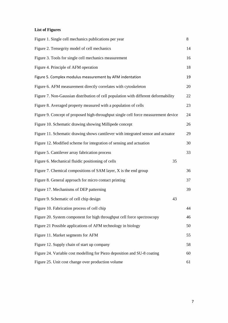
mechanical stimuli. As shown in Figure 1, the field of single cell mechanics has
gained increasing attention in past decades. It has become increasingly recognized in
past 20 years that not only chemical substances from hormone secretion or signalling
pathways affect the behaviours of cells, the mechanical interactions of cell and its
environment, which is related to the cytoskeleton resides in cytoplasm [1, 2], can also
dictate important changes in the life cycle of cells. For example, the transformation of
mesenchymal stem cells (MSCs) to matured functional cells such as osteocytes and
chondrocytes [3] during embryonic development involves the change of cytoskeleton
as well as the mechanic properties of the differentiating cells [4].
Figure 1. Single cell mechanics publications per year, data obtained from database Scopus
0
500
1000
1500
2000
2500
3000
3500
1970 1980 1990 2000 2010
Publications/Year
Publications/Year

9
The study of single cell mechanics involves the measurement of cell properties such
as quasi-static indentation stiffness [5], shear modulus [6], loss, storage, and complex
modulus in response to dynamic oscillatory loading [7] and relaxation time constants
[8]. The detecting of single cell mechanics can sometimes measures force and
displacement as small as a few pN and angstroms [9], these measurements impose
high requirements in terms of resolution, accuracy, response time and throughput on
measurement instruments. In this thesis, a novel technology of high-throughput cell
force spectroscopy will be proposed and analyzed in details in terms of system
components, fabrication process, technology limitations and potential future
developments. In addition, analysis on commercialization is also carried out,
including intellectual property research, market analysis, cost modelling and supply
chain positioning, to assess the feasibility of developing this technology.
1.2 Single Cell Mechanics
1.2.1 Single Cell Mechanics for Cell Characterization
Recent studies suggest single cell mechanics can be used to characterize cells in terms
of cell phenotype, origin and disease. In the research carried out by Darling et al [10],
the viscoelastic properties of cells were used as biomarkers to differentiate three cell
lines (chondrocytes, osteocytes and adipocytes) derived from mesenchymal stem cell
(MSC), so that all four cell lines can be separated. The group used commercially
available atomic force microscope (AFM) to perform indentation on cells, and
subsequently measured the stress relaxation time constant to estimate the elastic
modulus and viscoelastic modulus. They found in the experimental configuration,
when cells were adhered to substrate, there was significant difference (p<0.0001) in
elastic modulus and viscoelastic modulus among all four kinds of cells.
The logic of using single cell mechanics as a biomarker lies in the connection of
single cell mechanics and cytoskeleton; single cell mechanics manifest cytoskeleton
structure thus could be an indication of cell status [11]. Cytoskeleton is a network
composed of filamentous proteins of actin, tubulin or one of several classes of
intermediate filament [1], which are major contributors to the mechanical properties
of cells and are also responsible for intra cellular transportation as well as cell
10
locomotion [12, 13]. Cytoskeleton mechanically connects intra cellular structures to
extra cellular environment through the docking by transmembrane proteins such as
integrin and Neural Cell Adhesion Molecule (NCAM) on extra cellular matrix (ECM)
[14, 15].
It is found that cell deformability is related to cytoskeleton too, reduced assemble of
cytoskeleton increases the deformability [16]. When cells age, their cytoskeleton also
changes as there is a reduction in the amount of constituent biopolymers of
cytoskeleton [17, 18]; as a result, their elastic modulus and shear modulus decrease,
making them less resistive to external loading such as tension and shear [19]. In
another previously cited work [20], the author concluded single cell biomechanical
responses change due to cytoskeleton rearrangement.
Another obvious example demonstrating the correlation between single cell
mechanics and cytoskeleton is the phenotype of a single cell could be altered by the
decreased formation of actin, resulting in a morphological change which transforms
the cell into spherical shape with a chondrocytes-like morphology [21].
1.2.2 Single Cell Mechanics for Diseases Indication
Cytoskeleton’s material properties are able to affect the response of cells or tissue to
external loading. Cell or tissue’s abnormal responses to mechanical loadings can
induce various diseases, such as asthma, osteoporosis, atherosclerosis and diabetes;
and they contribute to the clinical presentation of these important diseases [22]. Since
single cell mechanics reflects the status of cytoskeleton, it is possible that the
measurement of mechanical properties of cell can indicate abnormalities in
cytoskeleton, thus may be potentially used for diagnostic purposes.
As a highway for signal transduction, cytoskeleton provides various localization
mechanisms for enzymes like glycolytic enzymes (aldolase, glyceralde hyde-3-
phosphate dehydrogenase, lactate dehydrogenase, and phosphofructokinase-1 [23]),
protein kinases (Tyrosine kinases [24], protein kinase C [25]), phospholipases
(phospholipase A2 [26]) and GTPases [27]. Upon the conformational change of
cytoskeleton under mechanical stimuli, the enzymes linked with the network have to
undergo architecture change correspondingly. If their conformations are altered, the

11
thermodynamic and kinetics of the chemical reactions will change inevitably.
Cytoskeleton also affects the transportation of ions or intracellular compartments; for
example, F-actin can affect the ion channels of Na+ and Ca
2+. When the assembly of
F-actin is prohibited by drugs like cytochalasins [28] in culture medium, the
measurements of ion flow from patch clamp experiment showed the conductivity of
these ions increased dramatically, however, upon stabilization of F-actin by adding
drugs like phalloidin [29], the conductivity of these channels dropped in comparison
with previous case. Thus, if an abnormal cell mechanics property is detected, it will
likely to manifest the mechanotransduction is impaired, either the ion channels or the
enzymes linked on cytoskeleton may not function properly.
As such, many diseases can be correlated with the dysfunction of cytoskeleton system,
and can be recognized with altered single cell mechanics. It has been recognized 20
years ago that cytoskeleton may be related liver illness [30]. Zatloukal and coworker
[31] have reviewed that in diseases like Alcoholic and non-alcoholic steatohepatitis
(ASH & NASH), Copper toxicosis, Cholestasis as well liver cancer, the degradation
of keratin filament and the disassemble of the intermediate filaments usually happen.
Besides, there is also imbalanced production of keratin subunits, so that the assembly
of keratin filaments is greatly hindered [32]. As a result, the cells loss the mechanical
support to physically maintain proper cell morphology and mechanical integrity,
resulting in the ballooning of the cell [33].
Cell mechanics can also be a marker for apoptosis, it has been shown that cells are
less resistive to internal stress due to degradation and restructuring of all three
cytoskeletal filaments. The change in mechanical properties of the cell may even
produce blebbing of cytoplasm membrane, which is the hallmark of programmed cell
death [34-37]. In experiment, cell death can be induced directly by applying drugs
like taxol and vinblastine to purposely disrupt of microtubule [22].
In cancer cells, deformability has been shown to be positively correlated with the
degradation of cytoskeleton and the metastatic rate. In the research carried out by
Ochalek et al [16], four variants of the same cell line with different metastatic rates
are tested for their mechanical deformability. In the experiment, the variant with the
least metastatic rate had the lowest deformability while the most metastatically
unstable variant had the highest stability. When all variants were treated with drugs

12
preventing the assembly of cytoskeleton, their deformability increased, strongly
suggesting a correlation between the involvement of the cytoskeleton and their
carcinogenic potential.
In another work by Suresh et al [20], single cell mechanics was used to characterize
two distinct human diseases: gastrointestinal cancer and malaria. During their
experiment, they found the elastic modulus of treated cancer cell to be significantly
different from that of untreated ones, and they suggested it could be due to the
reorganization of cytoskeleton near nucleus. In their test of red blood cell (RBC) in
vitro with optical tweezers, the shear modulus of RBC increased about 10 fold
because of parasite infection, resulting in the easy corruption of RBC when
experiencing high shear fields.
Suresh’s experiment results were further confirmed by the study of RBC mechanics
when RBCs from patients with sepsis and leukostasis were tested in microfluidic
devices [38]. The experiment subjected RBC to narrow fluidic channels where cells
had to deform in order to flow with fluids in the channel. It was shown RBCs from
patients suffering these hematologic diseases had a decreased deformability compared
to normal RBCs. The authors also concluded these diseases affected the status of
cytoskeleton, as when drugs affecting cytoskeleton (cytochalasin D and pentoxifylline)
were applied to RBCs, their deformability increased significantly.
Because of the important role cytoskeleton playing during the differentiation,
proliferation and other events in cell life cycles, the abnormality in cytoskeleton is the
source of many diseases. As previous examples showed, the measurement of single
cell mechanics reflects the status of cytoskeleton, it is thus important for the
understanding of cell biology as well as disease etiology to obtain this information
[39].
1.2.3 Modelling of Single Cell Mechanics
There are a few models relating the mechanical properties of cells to the measurement
done with various tools, thus bridging the macroscopic measurement with deeper
understanding of cytoskeleton.

13
Besides the mostly used model where cells are treated like homogenous viscoelastic
entities, the other widely used model to relate cell’s mechanical behaviours to
cytoskeleton is the tensegrity model. The stability of the system depends on tensional
integration, rather than compressional continuity. In this model, the cytoskeleton of a
cell is represented by a group of interconnected bars and viscoelastic cables. And it is
viewed that these structures are interconnected between cells in a tissue through the
mechanical linkage of ECM [40]. Upon loading, tensegrity structure tends to deform
globally rather than locally, that all its mechanical component can rearrange in order
to respond to the applied force [41].
Figure 2 shows one of this model, where 6 bars and 24 viscoelastic cables were used
to construct the model. In loading scenario, numerical analysis has to be used to solve
for loading response. In this particular example, four nodes are fixed in order to
simulate the attachment of cell to substrate surface. External loading can be applied
though any of the nodes. In most simulations, only first order deformation of bars is
considered, because higher order deformations will only become significant with
larger dimension, which is less relevant when modelling cells.
Tensegrity model has been shown to be able to predict the mechanical measurement
from experiment data, in fact, tensegrity model was adopted because its prediction
coincides with experiments data where measured cell’s elastic modulus increases
linearly with deformation [42]. Moreover, modified tensegrity model predicts
accurately that the global structural viscosity and global structural elasticity changes
proportional to the square of the size of cell [43]. In addition, tensegrity represents the
combined mechanical behaviours of cytoskeleton components. Like F-actin, though
each single component of tensegrity does not exhibit linear increase of elastic
modulus under loading, The combined network showed linear increase in elastic
modulus just as combined F-actin network [44]. There may even be some connection
between the structures of tensegrity network to physical cytoskeleton structures. In
cytoskeleton systems, microfilament (MF) can produce internal stress through internal
actomyosin sliding as the viscoelastic cable in tensegrity model, and the stiffness of
MF can be altered with different concentration of crosslink proteins among molecules
[45, 46].
14
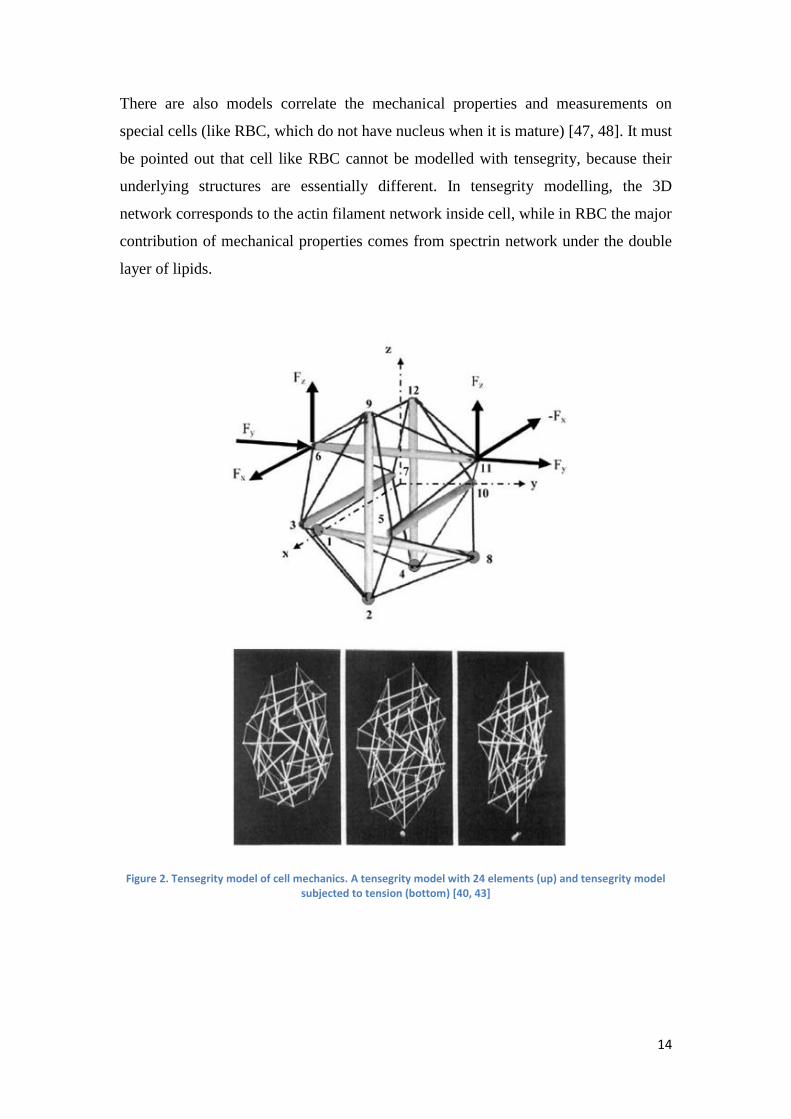
There are also models correlate the mechanical properties and measurements on
special cells (like RBC, which do not have nucleus when it is mature) [47, 48]. It must
be pointed out that cell like RBC cannot be modelled with tensegrity, because their
underlying structures are essentially different. In tensegrity modelling, the 3D
network corresponds to the actin filament network inside cell, while in RBC the major
contribution of mechanical properties comes from spectrin network under the double
layer of lipids.
Figure 2. Tensegrity model of cell mechanics. A tensegrity model with 24 elements (up) and tensegrity model subjected to tension (bottom) [40, 43]
15
1.3 Tools for Mechanical Properties Measurement
In the past 20 years, single cell mechanics has gained increasing interest in the
research community. Since physical measurement can be correlated to the status of
cytoskeleton, it has been of great interest to develop measurement instruments for
probing the mechanical properties of single cells. There have been numerous tools
developed for this purpose, the earliest of which is the use of micropipette to perform
aspiration [49, 50] on nontransformed and transformed cells. Micropipettes are
generally made by pulling hot glass capillary tubes. Suction can be applied to cell
surface once micropipette is attached to the target cell. The deformation of the cell
measured with respect to time reveals the viscoelastic properties [51]. For example,
in the measurement of viscosity of blood granulocytes, the experiments revealed that
the viscosity of the cell changes with respect to temperature, from 2×10³
poise at 27°C
to 103 poise at 37°C [52]. Micropipette aspiration has also been used in measuring the
Poison’s ratio of chondrocytes and osteocytes in [51], which ranges from 0.36 to 0.38.
Magnetic bead microrheology is another technique used in measuring the mechanical
properties of cells [53]. In this kind of set up, magnetic beads functionalized with
ligands that can attach to cell surface are used. When magnetic field is applied,
tangential force exerts onto the surface of cells by the magnetic beads. In [53], the
shear modulus of fibroblasts is measured to range from 2×10⁻³
Pa m̟ to 4×10⁻³
Pa˖m.
The authors also found the bulk shear modulus to be 0.5×10⁻⁴
Pa, membrane
coefficient of friction of to be 2×10⁹ Pa s̟/m corresponding and cytoplasmic viscosity
of 2×10³ Pa s̟. By using this tool, it is also revealed that cells can be viewed as
composited of materials near their glass transition temperature, and cytoskeleton
modulate cell’s responses to mechanical stimuli by altering effective noise
temperature of the matrix [54]. A scaling law of elastic and frictional properties and
was observed between different kinds of cells [54]. Another similar too is optical
tweezers, which uses similar principles to measure local mechanical properties of
cells by utilizing laser deflection particles [55, 56]. In [55], the authors estimated the
local shear modulus of red blood cell membrane to be 2 x 10⁻⁶
Nm-1
.
Osmotic loading subjects cells to different osmotic pressures and detects the change in
cellular volume, which is an indication of whole cell mechanical properties [57].
Through the use of osmotic loading, it is found the normalized volume of cells change

16
linearly with respect to osmotic pressure, and the instantaneous and equilibrium
elastic moduli as well as the apparent viscosity of the cells were significantly
decreased by hypoosmotic loading, but were unchanged by hyperosmotic loading [58].
Figure 3. Tools for single cell mechanics measurement [59].
Other techniques quantifying whole cell mechanical property include rheology
measurement by plating manipulation where the cell is attached and traction or
uniaxial compression is applied through the deformation of the plate or the plate, the
applied force and measured displacement are in Newton and mm range respectively.
Microplating is also possible where the resolution of this technique can be increased.
In the experiment reported in [60], microplating was used to measure the loss and
storage modulus of single HeLa cells. The authors found the storage modulus to be
around 660 Pa when stimulation was performed at a frequency of 1 Hz, which is quite
close to the AFM measurement result at low frequency. Microfluidic devices can also
be used for measuring the mechanical properties of single cells, like their resistance to
shear or their ability to deform [61].

17
1.3.1 Mechanical Probing by AFM
Among the characterization techniques, one important probing method is the use of
AFM to quantify single cell mechanics. Atomic Force Microscope (AFM) is a unique
tool which enables high resolution measurement of the mechanical properties at sub
nanometer level [62]. In addition, unlike other high resolution scanning probe
microscopes, in situ force measurement on biosamples is also possible because AFM
can operate in a wide range of environments [63, 64].
AFM is developed from scanning tunnelling microscope (STM); it was originally
designed for the detection of the interactions between probe tip and substrate surface.
It provides flexible measurement of surface topography, friction, surface adhesion and
deformation [65]. Typical AFM probes consist of a deflectable cantilever and a tip at
one end of the cantilever. The cantilever must be resistive to deflection in two
directions while prone to deflection in the third direction. Typically, cantilevers are
fabricated so that their resonance frequency is above 10 kHz [66]. The cantilever
structure can be as large as a few micrometers, while the radius of curvature of the
end of tip can fall below a few nano meters (10nm for Si and 20-50 nm for SiN [66]).
The tip of AFM is usually fabricated from silicon or silicon nitride, which moves into
close proximity to interact with sample surfaces. AFM tip can be coated with various
materials for alteration of mechanical, thermal and electrical properties [67-71].
AFM probe interacts with sample with both short range and long range forces; van der
Waal forces act between sample and probe tip, while other forces such as electrostatic
force capillary force, chemical force as well as Casimir force can also play a part in
measurement. Because measurement is done by force interaction, no fixation or
staining of sample is required, thus the device is particularly suitable for the testing of
living tissue. The device is also able to quantify both static and dynamic loading
responses of cell by applying forces at different frequencies controlled by piezo force
generator relayed to an external signal generator.
AFM measures samples with length scale from a single molecule to a whole cell, with
a force range from several pico newton to nano newton. AFM obtains force-
displacement curves, which reveals elastic modulus of cells [72, 73]. In addition,
hystereses between approach and retraction curves can be used to evaluate the time-
dependent modulus and time constant [74].

18
Figure 4. Principle of AFM operation [64]
AFM typically operates in three modes, namely, contact mode, noncontact mode and
tapping mode. In contact mode, total force felt by the cantilever tip is repulsive. In
noncontact mode, total force exerted on the tip of cantilever is often attractive, and
atomic resolution is achievable [75]. And due to the shape of the potential well of van
der Waal interactions, there will always be a distance region that the AFM probe is
unable to work in with, as such, the measurement can only achieve a lower resolution
[66].
Typically, biosamples are measured in noncontact/tapping mode, not only to achieve
higher resolution, but also to prevent the destruction of sample by indentation or
friction between tip and sample. In noncontact/tapping mode, the cantilever is usually
driven at a preset frequency. A change in the frequency of vibration corresponds to
the external force felt by the cantilever. The following relationship shows the
estimation of force by detecting the modulation of frequency, where k is the stiffness
of a single leg cantilever beam.
1
2
f F
f k x

19
AFM has been used to probe cell surface elasticity. For example, one of the
pioneering studies of using AFM to probe the mechanics of single cell was carried out
in 1994 by Hoh and Schoenenberge [62, 76], in their experiment, they measured the
elastic modulus of MDCK and R5 cell and cellular dynamics with time lapse AFM.
AFM indentation on cells revealed the loss and storage moduli follows power law,
where the complex modulus at any frequency can be expressed as a base complex
modulus times the power of that frequency over the base frequency. For example, in
the measurement of complex modulus of human lung epithelial cells [77], the group
found both storage and loss modulus increased with indentation frequency up to 100
Hz. The exponent for storage modulus was measured to be around 0.2, and the
exponent for the loss modulus was measured to be around 0.067.
Figure 5. Complex modulus measurement by AFM indentation [77]
Because of the high resolution from AFM, there has been experiments using AFM for
cell regional force mapping, for example, in [6], the group used AFM to detect the
loss and storage modulus at nucleus region and peripheral regions respectively. The
group found the storage and loss modulus to be around 300 Pa and 95 Pa respectively
when indentation is performed at 0.1 Hz at nuclear region. However, the peripheral
regions were found to be more rigid than nuclear region at all indentation frequencies.
20
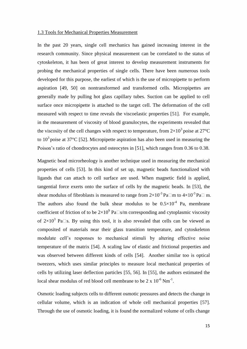
It is also possible to directly connect the measured mechanical properties with
cytoskeleton structures in living cells thanks to the high resolution of AFM. In the
work done by Christian Rotsch and Manfred Radmacher [78], it has been shown that
AFM measurement directly correlates with the cytoskeleton structure; and can reflect
the change of cytoskeleton upon the addition of drugs. In their experiment, NRK
fibroblasts were measured in contact mode with an AFM from Veeco ® and a force
map was generated from AFM measurement. Elastic modulus was then obtained from
force displacement curve of the AFM measurement. The cells were subsequently
stained with dyes that were selective to F-actin. As the following figure shows, the
features on AFM force map correspond to the stained structure by the dye, confirming
that AFM can directly probe cytoskeleton. In addition, when cytochilatin was used to
prevent the assembling of cytoskeleton, AFM measurement showed less features and
a decreased elastic modulus.
AFM can also accommodate to wide range of cells, not only eukaryotic cells can be
probed, prokaryotic cells like bacteria are also suitable for AFM investigation. For
example, the surface elasticity of bacteria M. gryphiswaldense was determined by
applying compressional stress on cell wall [79].
Figure 6. AFM measurement directly correlates with cytoskeleton. NRK fibroblast (a), AFM image (b), magnified view of AFM image (c), cytoskeleton staining (d), magnified view of staining (e) force map (f) [78]
21
Chapter 2 High Throughput Single Cell Measurement Technology
Although it has been demonstrated that the single cell mechanics can be quantitatively
assessed by a range of techniques mentioned previously, it is important to realize that
most of these techniques are of extreme low throughput, i.e. only capable of handling
a limited number of cells in a reasonable experiment time frame [80]. As a result, the
data produced by these techniques may not be an accurate reflection of the actual
status of a whole cell population.
This represents certain limitation when it comes to the measurement of any
heterogeneous cell population, which is often the case if the measurement is done on
any sample derived from living organisms. As it is now known that in any biological
events like growth, development and disease, there involves a coordinated reaction of
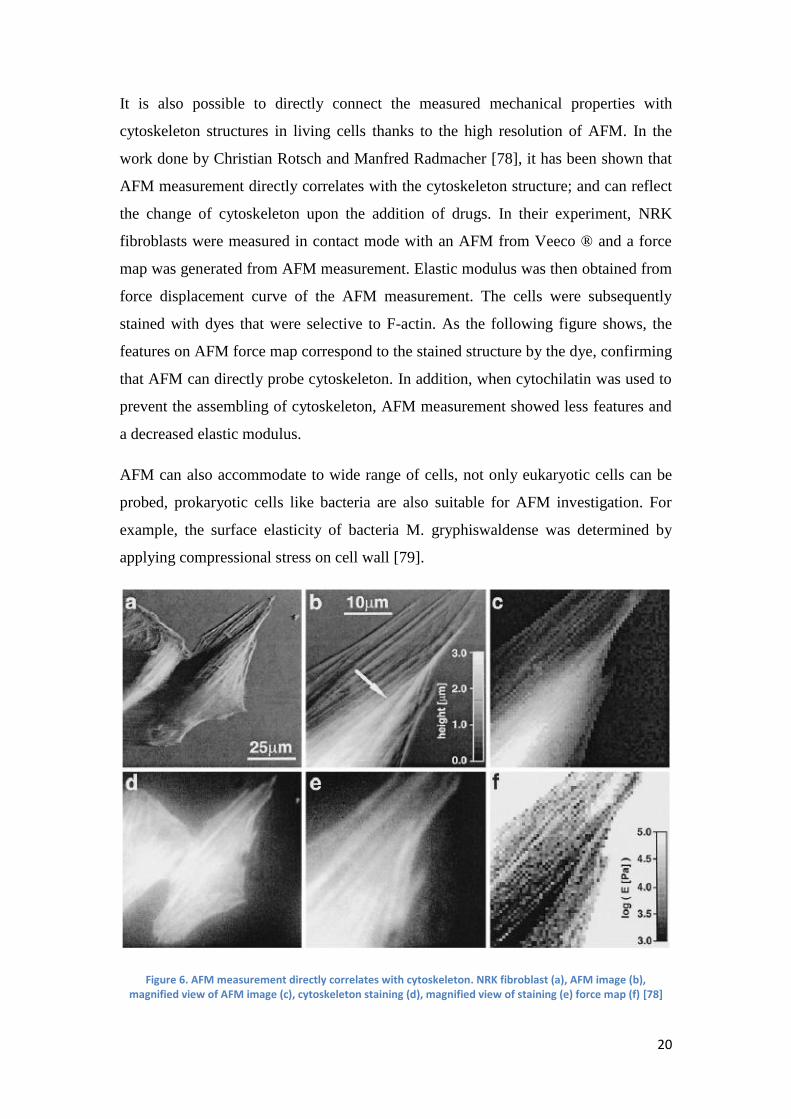
a heterogeneous population of cells [81]. It is also noted that the distribution of the
measured mechanical properties may not always be the same as assumed [38]. One
example was given in the measurement of cell deformability through microfluidic
devices. The passing time of RBC through a channel was recorded and used as a
parameter to represent single cell mechanics As shown in the following figure,
contrary to common assumption that a Gaussian distribution should characterize the
transit time, the cells derived from patients with hematologic diseases exhibited non-
Gaussian distribution that the majority of the cell population either pass within 2
seconds or will not pass within 8 seconds.
Moreover, when tested with neutrophil, control group exhibited dramatic differences
with group treated with drugs inducing inflammation, suggesting the distribution of
cellular mechanical properties can also be related to the status of the cells, thus could
be useful for characterization and diagnosis. It is also important to determine how the
different parts of metabolism are coordinated and balanced through the study of
heterogeneous cell population. The lack of distribution information could represent a
flaw in measurement.
22
Figure 7. Non-Gaussian distribution of cell population with different deformability [38]
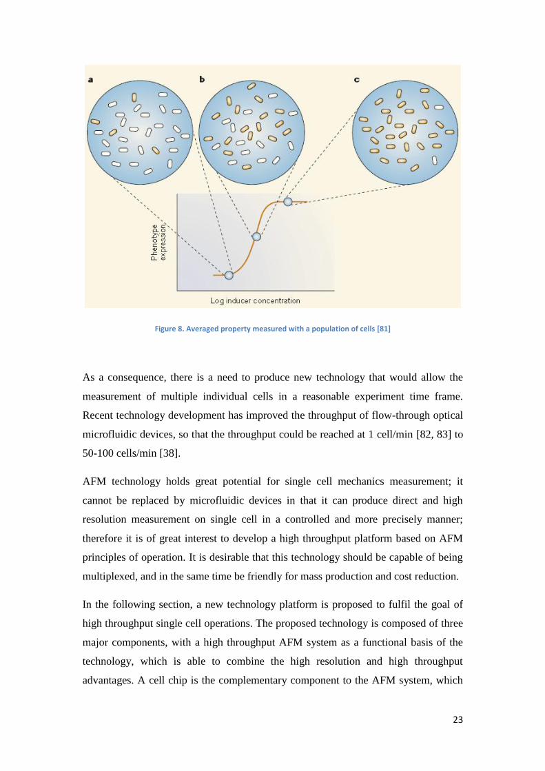
Furthermore, it must be stressed that although some techniques do measure the
property of a large number of cells, it is quite often the average properties of the
whole population are finally presented. For example, an increase in fluorescent
measurement of a clone can indicate higher activities of bacteria in that clone,
however, the measurement may not be an accurate indication of cell status as it could
mean either each cell has an increase in their activity level, or more cells turns from
“off” state to “on” state.
23
Figure 8. Averaged property measured with a population of cells [81]
As a consequence, there is a need to produce new technology that would allow the
measurement of multiple individual cells in a reasonable experiment time frame.
Recent technology development has improved the throughput of flow-through optical
microfluidic devices, so that the throughput could be reached at 1 cell/min [82, 83] to
50-100 cells/min [38].
AFM technology holds great potential for single cell mechanics measurement; it
cannot be replaced by microfluidic devices in that it can produce direct and high
resolution measurement on single cell in a controlled and more precisely manner;
therefore it is of great interest to develop a high throughput platform based on AFM
principles of operation. It is desirable that this technology should be capable of being
multiplexed, and in the same time be friendly for mass production and cost reduction.
In the following section, a new technology platform is proposed to fulfil the goal of
high throughput single cell operations. The proposed technology is composed of three
major components, with a high throughput AFM system as a functional basis of the
technology, which is able to combine the high resolution and high throughput
advantages. A cell chip is the complementary component to the AFM system, which
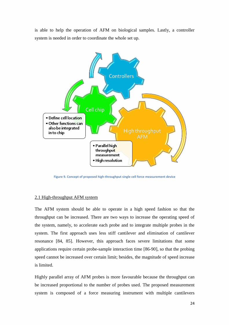
24
is able to help the operation of AFM on biological samples. Lastly, a controller
system is needed in order to coordinate the whole set up.
Figure 9. Concept of proposed high-throughput single cell force measurement device
2.1 High-throughput AFM system
The AFM system should be able to operate in a high speed fashion so that the
throughput can be increased. There are two ways to increase the operating speed of
the system, namely, to accelerate each probe and to integrate multiple probes in the
system. The first approach uses less stiff cantilever and elimination of cantilever
resonance [84, 85]. However, this approach faces severe limitations that some
applications require certain probe-sample interaction time [86-90], so that the probing
speed cannot be increased over certain limit; besides, the magnitude of speed increase
is limited.
Highly parallel array of AFM probes is more favourable because the throughput can
be increased proportional to the number of probes used. The proposed measurement
system is composed of a force measuring instrument with multiple cantilevers
25
functioning as AFM tip array and cell chip for the precise positioning of cells. In
addition, a controlling system is necessary in order to coordinate the two components
and to analyse the acquired data.
The proposed device employs an array of AFM tips individually controlled by
picoforce piezos. There is a cell chip loaded on a platform and is controlled by three
motors so that it could move in X, Y and Z directions independently. With this
configuration, multiple cells can be tested simultaneously in one round, with each cell
measured by one AFM tip, and the next round of readout can be obtained be moving
platform to next designated coordinates.
The proposed device should have much higher throughput compared to conventional
AFM, thus it can be used for high throughput cell mechanical property testing for cell
biology study. Besides, this device should be able to test bioproducts such as
engineered tissue, single cell mechanical testing is commonly used as a merit metrics
of engineered tissue performance.
The number of cells tested per round is determined by the number of AFM tips in the
array. Carrying out the testing for several rounds does not only generate averaged
properties of the tested batch of cells, but also produces statistical information of this
batch. Distributions, variations and deviations of mechanical properties can be
obtained for better characterization of not only a single cell, but also of a group of
cells. Generally speaking, two categories of such devices are mostly developed. The
first category consists of device primarily developed by IBM (termed “millipede”
system) [91].
2.1.1 Millipede Array
IBM Research Division, Zurich Research Laboratory presented a scheme using a
square array of AFM cantilevers for patterning polymer by indentation [91], where
32×32 (1024) probes were used to create patterns on substrate surface. The following
figure demonstrated the concept of IBM’s parallel array “millipede”.

26
Figure 10. Schematic drawing showing Millipede concept [92]
The millipede device consists of a square array of cantilevers arranged in a row-
column manner. Each cantilever is in charge of a field about 100µm × 100µm [93].
The cantilevers are entirely fabricated from silicon for good thermal and mechanical
properties through surface micromachining by either plasma etching or wet etching
[88]. Each cantilever consists of two legs acting as soft springs; legs are highly doped
to reduce the resistance and energy dissipation, while tip is lightly doped. Metal
wirings are avoided on leg region to avoid any electron migration or parasitic effect.
Legs are specifically produced with less mechanical stiffness to reduce the force
required for deformation, so that the tip and substrate can be well protected [88].
The unique point about this millipede system is that whole array is controlled by only
one z-scanner, so that the complexity of the system can be reduced [93]. However,
several z-scanners can be used if more precise control of the vertical position of the
array is needed [94]. As a result, the system requires uniform substrate surface to
avoid the damage of the array. When approaching substrate surface, four cantilevers
integrated at the corners of the array will detect the tilt of the substrate relative to the
array [88].
The cantilevers in this array are not mechanically coupled and can be individually
actuated by the application of voltage pulse [93]. When actuation is performed, each

27
individual cantilever receives two electrical pulses from the row and column it
belongs to, if the sum of the pulses is nonzero, an indentation action will be
performed [95].
A more complex array of 64×64 (4096) cantilevers has been fabricated [94],
Demonstrating the possibility of building high throughput devices by this approach.
However, the application of millipede system to biological sample faces severe
limitation. The millipede system is controlled by only one z-scanner [93]. Although
this setup reduces the system complexity, it requires uniform substrate surface to
avoid the damage of the array. Due to inherent surface roughness of biological
samples, the variation in z direction can be as huge as several microns, which may
disable the probing of the array to the surface. In addition, though the cantilevers are
not mechanically coupled, their signals are coupled because the signal is transmitted
in rows and columns, i.e., cantilevers in the same row will receive the same actuation
signal (amplitude) transmitted by that row, so do cantilevers in the same column. As a
result, the cantilever array lacks the ability to control each cantilever flexibly.
Furthermore, each actuation made by the cantilever is static, rather than vibrational
actuation used in tapping mode or non-contact mode AFM, which is more likely to
destroy soft materials. Another restriction of the millipede array comes from the
probing method and response time; IBM chose to use heat conduction to probe-
sample distance, and with the measurement of resistance change to detect beam
deflection. Both detection and actuation is too slow and too inefficient [96] for
probing soft tissue because temperature change has to overcome the heat capacity of
cantilever and heat dissipation to environment [94].
2.1.2 Individually Controlled Cantilever with Sensor and Actuator
The other kind of cantilever array is composed of individually controlled cantilevers
with integrated sensing and actuation functionality. A High number of cantilevers
form the self-actuated arrays, and these arrays can be further integrated into a large
scale array for achieving even higher throughput [97]. For achieving actuation
functionality, the cantilevers in this case mainly use piezoelectric materials, which can
transfer the externally applied voltage into strain. This sort of array is generally faster
in operation [98].

28
The piezoelectric material used could be materials from group III-V or group II-V
compound materials, for example, ZnO is the most widely used piezoelectric material
in MEMS, in addition, AlxGa1-xAs and Pb(ZrTi)O [99] can also be used for higher
piezo constant [100].
The pioneering work of the use of parallel scanning probes with individually
controlled cantilevers was initially used by S. C. Minne in 1994 [101] to pattern
amorphous silicon on single crystal silicon 100 surface as a lithography mask. Early
developments from the group used one array of two piezoresistive cantilevers, with
one in feedback loop set to constant force of 600 nN and the other in an open loop.
Both cantilevers were operated under the condition of 20V bias voltage. They
discovered that individual feedback of the cantilevers must be established in order to
achieve high precision force control. The group also used arrays of four parallel
cantilevers to image 100μm × 400μm surface with the same amount of the time
usually only sufficient for 100μm × 100μm square area. Thus it corresponds to a 3
fold increase in throughput in the parallel cantilever system.
However, this group did not manage to integrate the sensing function onto each
cantilever in the array, they used laser deflection detector to probe the cantilever
bending. When larger number (4 cantilevers) of cantilevers was used, due to limited
space, they were not able to use one laser deflector for each cantilever, so individual
control was not achieved. As such, the author concluded further development on
integration of sensing with AFM array is the key to the application of AFM array with
large number of cantilevers for high precision operations.
The integration of the sensing unit in cantilever itself is necessary, because it greatly
reduces the space needed for sensing modules. As illustrated in Figure 4, conventional
AFM employs laser and photodiode set up for the purpose of cantilever beam
deflection detection. For low level integrations of AFM like in previous case,
separated sensing unit has already shown its limitations. As such, for the integration
of a higher number of cantilevers, it would be impossible to continue to use the
separated sensor and cantilever design.
There are a few categories of sensors that can be readily incorporated onto cantilevers,
for example, capacitors [102, 103] can be built onto the cantilevers for sensing.
Piezoelectric materials can also be incorporated onto the cantilevers for the detection

29
of beam deflection by measuring the voltage across the material. Another way to
integrate the sensing functionality onto the cantilever is to use piezoresistive effect of
silicon. It has been demonstrated that the resistivity of silicon could change upon
deflection, although no charge is produced. One example of using piezoresistive
sensing is demonstrated below in [98] and improved in 1996 [104], where the sensor
and actuator were integrated onto cantilever together. The following figure shows one
of the cantilevers in the array.
The design uses V shaped leg for achieving the sensing functionality, where the
bending of the cantilevers can be transferred into the resistance change along the V
shaped leg. Current is passed through the V shaped support from one leg to another.
The change in the resistance will induce the change in current so that the deflection
can be calculated.
Figure 11. Schematic drawing shows cantilever with integrated sensor and actuator [98]
The cantilever beam is deposited with a layer of 3.5 μm thick ZnO on top of the Si
beam. If a field is applied in the direction of the beam, the cantilever will bend due to
the expansion of ZnO. Below the silicon oxide insulator, the doped Si functions as a
piezoresistor to detect the bending of the beam.
30
However, this design suffers inherent flaw that the piezoresistor sensor spans the
entire range under ZnO actuator; it detects not only the bending caused by force on tip,
but also the bending of ZnO actuator itself. The signal thus has to be electronically
compensated for correct reading.
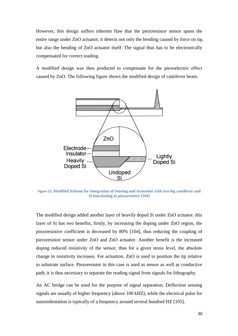
A modified design was then produced to compensate for the piezoelectric effect
caused by ZnO. The following figure shows the modified design of cantilever beam.
Figure 13. Modified Scheme for Integration of Sensing and Actuation with two-leg cantilever and
Si functioning as piezoresistor [104]
The modified design added another layer of heavily doped Si under ZnO actuator. this
layer of Si has two benefits, firstly, by increasing the doping under ZnO region, the
piezoresistive coefficient is decreased by 80% [104], thus reducing the coupling of
piezoresistor sensor under ZnO and ZnO actuator. Another benefit is the increased
doping reduced resistivity of the sensor, thus for a given stress level, the absolute
change in resistivity increases. For actuation, ZnO is used to position the tip relative
to substrate surface. Piezoresistor in this case is used as sensor as well as conductive
path; it is thus necessary to separate the reading signal from signals for lithography.
An AC bridge can be used for the purpose of signal separation. Deflection sensing
signals are usually of higher frequency (above 100 kHZ), while the electrical pulse for
nanoindentation is typically of a frequency around several hundred HZ [105].
31
2.1.3 Cantilever Array Design
The proposed cantilever array will utilize piezoelectric materials for the purpose of
sensing and actuation. Unlike in the case of capacitor sensor and piezoresistive sensor,
where sensing and actuation are carried out by separate structures, the sensing and
actuation function can be achieved by the same piezoelectric material, thus it is ideal
for the purpose of integration. It has been demonstrated that perovskite structured
materials usually have higher piezoelectric constants, and can be used for MEMS
application with conventional planar processing techniques [106]. Although AlGaAs
materials also offer high piezoelectric coefficient, the fabrication of such materials
typically needs sputtering or MOCVD, which increases the cost of fabrication. On the
other hand, the fabrication of perovskite materials can be achieved with simple
method as spin coating, which does not add significant cost on the production. As
such, perovskite structured material is chosen as actuator material for cantilevers.
Pb(Zr,Ti)O3 is chosen for actuator fabrication. The fabrication process is modeled
below. A single leg design of the cantilever beam is chosen; compared with the V
shaped, single leg cantilever takes less space, so integration can achieve higher
density. However, it cannot use the piezoresistive effect for sensing as it’s difficult to
use single leg silicon as piezoresistor without short circuit. As such, an alternative is
to measure the deflection of the PZT material itself by the electric potential it
produces.
The proposed cantilever array must fulfil the requirement for cell testing and in the
same time be compatible with fabrication technologies currently used in industries.
The design of this device is inspired by the work of Itoh et al. [99].
For the adaption of this device to the testing of cells, the array must be able to
accommodate the possible variations in cell size. As a result, a longer cantilever
length is needed so that more deflection can happen over the whole cantilever range.
And if the variation of cell size does occur at some position, DC voltage could be
applied to specifically deflect the cantilevers at these positions. However, the use of
long cantilever will produce a lower the first resonance frequency [107, 108],
producing a lower sensing speed in tapping and non-contact mode. To counter this
problem, short cantilevers could be used with actuators producing larger force, so that
both large deflection and fast sensing can be achieved simultaneously.
32
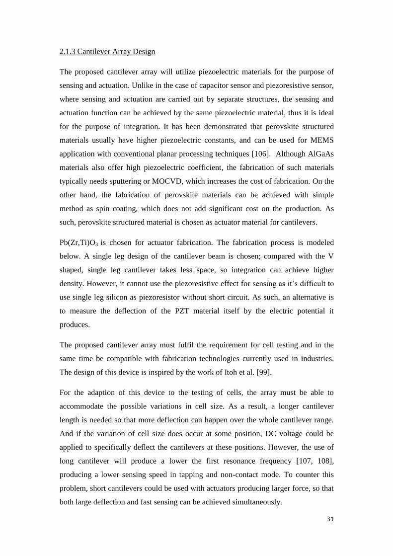
The fabrication process of the device is modelled below:
A. A photoresist layer is deposited on Si substrate (yellow), and then holes
corresponding to the base diameter of tip are made by exposing the resist. Cr
deposition is carried out and followed by a lift off process, so that circular Cr
patches (black) of the same diameter as the base of the tips are produced.
B. Reactive ion etching is carried out so that silicon columns are created at the
positions of tips.
C. Thermal oxidation is carried out to change Si to SiO2, and then the substrate is
submerged with KOH which etch the columns into tips.
D. A layer of Pt (green) is deposited by sputtering on the desired location of
substrate; the Pt layer will later be patterned into one set of electrodes.
E. The PZT layer (blue) is prepared by a Sol-gel process. To prepare Pb(Zr,Ti)O3,
zirconium-n-butoxide dissolved first in glacial acetic acid, 2-propanol, and 1-
butano [109], subsequently, Ti{OCH(CH3)2}4 and Pb(CH3COO)2 are also
dissolved in the solution. The mixture is hydrolyzed before cross link agent
ethylene glycol is added. The solution is further dissolved by 2-propanol and
1-butanol and acetic acid before deposition. The method is derived from
reference [110, 111].
F. To deposit the PZT material on substrate, spin coating is carried out followed
by baking. Multiple spin coatings are necessary in order to achieve the desired
thickness of the PZT material. After the last spin coating, the structure should
be moved to an oven for annealing at 600 degrees to facilitate the formation of
perovskite structure.
G. Another layer of Au (pink) is deposited on top of the PZT material, to function as the
other set of electrodes.
H. The final step is to etch away undesired part by dry etching, and then a layer of SiO2
is sputtered to passivate the deivce.
It is already shown this approach can be used for batch fabrication of up to 50
cantilevers. Batch fabrication of an array with higher number of cantilevers is possible
[99, 112]. However, it is probably more favourable to use more such arrays to
integrate into a higher level array, so that modular design can be achieved. In the case
of cantilevers break down, it would not be necessary to replace the whole array,
instead, only the sub array containing the broken cantilever needs to be replaced.

33
The device is operated by applying voltages between two electrodes (green and pink
layers). DC voltage induces a static deflection while AC voltage induces dynamic
actuation. A small amount of tip displace can be applied on each cell and the
corresponding force can be measured. To detect the responses of cells, the voltage
generated by the bending of PZT between the two electrodes is monitored.
The group by Itoh showed cantilevers can be fabricated in this manner to achieve a
resonance frequency about 64 kHz and actuation sensitivity of 150 nm/V. In addition,
they also demonstrated their cantilevers can accommodate a sample variance at z
direction as large as 1.5 µm [99] with the length of cantilever equal to 200 µm.
Figure 13. Cantilever array fabrication process

34
2.2 Cell Chip
Due to the employment of cantilever array, cells have to be precisely placed on
substrate at corresponding positions to cantilever tips. In addition, substrate has to
provide sufficient affinity so that cells will not be displaced by the force applied by
cantilever tip. A cell chip is necessary to fulfil these requirements. It has been shown
that small particles and cells can be precisely manipulated by vibration force (acoustic
tweezers), hydrodynamic force (microfluidic tweezers) and optical force (laser
tweezers) [113]. However, these methods require extensive labour if large quantity of
cells are to be manipulated.
When coupled with other technology, recent advances in MEMS application provide
simple methods for achieving precise positioning for a large quantity of cells. MEMS
based positioning methods can be generally characterized into positioning by optical
guiding, by mechanical fluidic trapping, by chemical modification and by the
application of electric fields.
Optical guiding involves the use of laser, which can generate forces in piconewton
range (up to 300 pN [114]) for manipulating small particles. The force is generated
with a high power focused laser beam passing through the dielectric particle. When
placed around the beam waist, the dielectric particle feels the greatest force due to the
largest electric field gradient. It is also necessary to build an environment so that the
light travels in a medium with refractory index different from that of the particle [115].
A high throughput laser positioning system involves the use of hollow optical fibre,
where laser carries cells from source to the hollow optical fibre [116]. By the guiding
of the optical fibre, cells can be deposited when they exit from the other end of the
fibre. By moving the fibre, arbitrary patterns can be formed on the target. It has been
demonstrated that this positioning technique can achieve a resolution under 1 µm at a
very high particle fluxes up to 10 kHz [117]. However, some drawback of this
technique hinders its application to biological samples, as moving cells require very
high power, the concern of viability of single cells subjected to the laser arises [118].
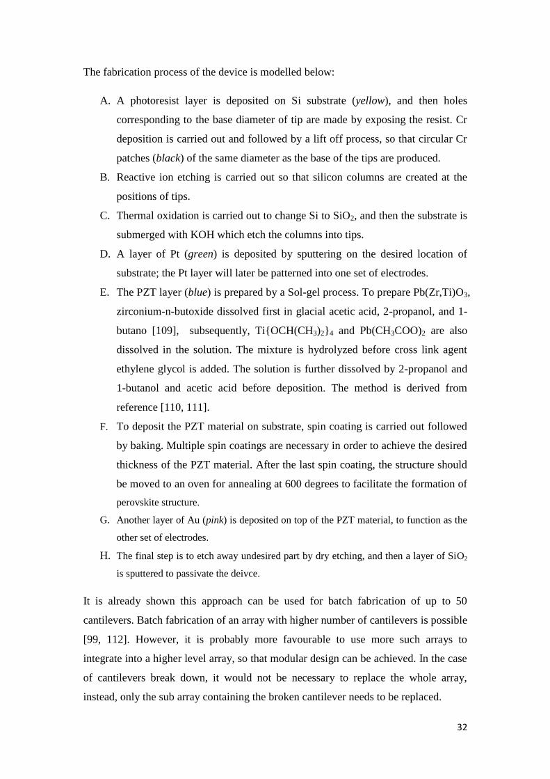
Mechanical fluidic patterning uses patterned structures to disturb the flow of cells in
the laminar flow of liquid and selectively trap cells at desired location. Examples of
this kind of positioning include the use of dam/overflow structures [119] or sandbag
35
structures [120]. In dam structure, the flow is blocked by dam perpendicular to the
flow direction, and cells are deposited at the foot of dam. The problem of this design
is the difference of the hydrodynamic pressure across dam structure is too great, that
multiple rows of cells can be deposited at some position, inducing undesirable cell
aggregation at certain location. The modified overflow design uses two parallel
channels with different hydrodynamic pressure; the hydrodynamic pressure difference
can be controlled such that only a single row of cells is deposited.
Figure 14. Mechanical fluidic positioning of cells. Dam (up left) and modified overflow (up right) design, sandbag design (bottom) [119] and [120]
Similarly, sandbag structures fabricated from photolithographic processes also
partially block the flow in channel. Although majority of the liquid flows along the
arrow (arrows shown in figure) direction, a small portion of fluid flow over the sand
bag and bring cells to be deposited at the depicted positions (red circles). Other
36
designs uses similar principles may involve the use of microwells in channel. A two-
step process has been reported by Langer [121] to use poly(ethylene glycol) (PEG) to
fabricate wells within micro channels for accurate positioning.
Chemical modification is another widely used technique to confine cell in certain
positions. Typical chemical modification involves the deposition of protein prior to
the deposition of cells [122]. Many of these deposited proteins are extracted from
ECM, like fibronectin (FN), collagen I, collagen II and Laminin [122, 123]. Proteins
can be deposited through a photolithography process with lift off. Synthesized poly
peptide can also be used for depositing. The common feature of this kind of poly
peptide is that they contain a tail sequence of Arg-Gly-Asp (RGD) tri-amino acids
[124]. It is believed RGD is one of the primary recognition sequences for integrin
[125, 126], which is a transmembrane protein for regulating a host of cell responses
including cell focal adhesion. Other materials, such as selectin, enzymes and antibody
[127] can also be deposited on substrates to enhance cell adherence.
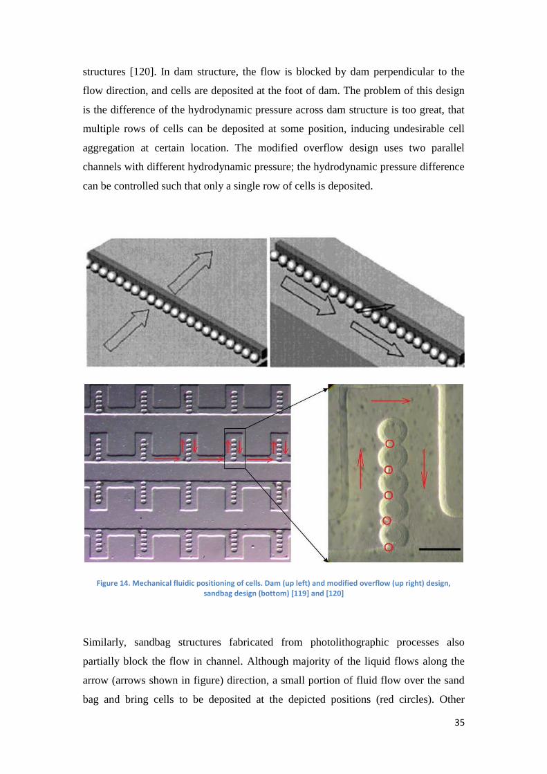
Another approach of chemical surface modification employs a technique named micro
contact printing [128, 129]. Before printing, soft lithography is usually carried out to
produce a stamp with polymers like PDMS. Self-assembled monolayers (SAMs) are
printed with stamps onto substrate which is surface-modified by gold, silver or
titanium deposition [128]. The stamp defines the positions for SAMs deposition. This
printed pattern can form a ultra thin mask (10nm) for subsequent deposition of
another material, or it could be used directly as created patterns.
Figure 15. Chemical compositions of SAM layer, X is the end group [124]

37
Most widely used SAMs are alkanethiolates with different end groups. It is found
SAMs terminated with methyl groups adsorb proteins while SAMs terminated with
oligo (ethylene glycol) are extremely resistant for protein adsorption. Thus, SAMs can
be used to link previously mentioned biomolecules with substrate. In addition, cells
can directly attach to SAMs, it is found that the adherence strength of cells on SAMs
layer is greatest with SAMs terminated with hydroxyl group, followed by SAMs
terminated with carboxyl group and amino group, the adherence is the lowest with
SAMs terminated with methyl group [124].
Figure 16. General approach for micro contact printing. Molding of PDMS soft stamp from patterned master (a), Peel off PDMS stamp (b), stamp in contact with SAM ink (c), PDMS print on substrate (d) SAM layer produced
as mask (e), Deposition of a secondary SAM (f) [128]
38
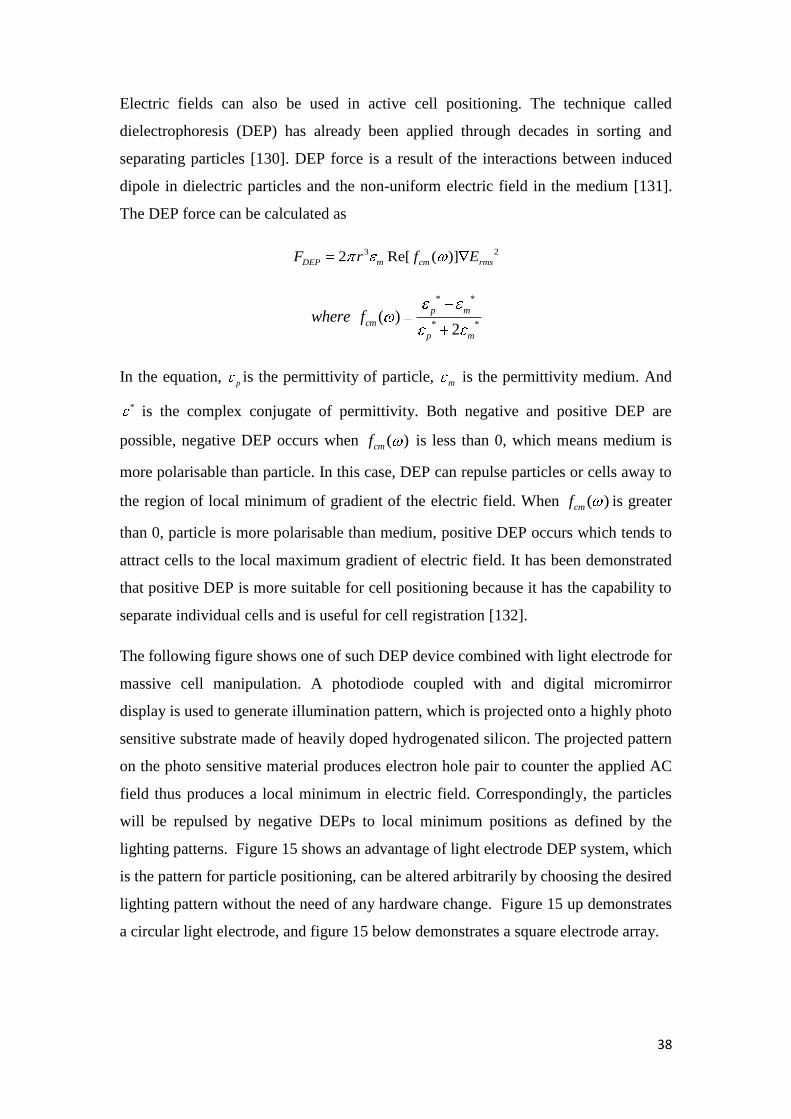
Electric fields can also be used in active cell positioning. The technique called
dielectrophoresis (DEP) has already been applied through decades in sorting and
separating particles [130]. DEP force is a result of the interactions between induced
dipole in dielectric particles and the non-uniform electric field in the medium [131].
The DEP force can be calculated as
3 22 Re[ ( )]DEP m cm rmsF r f E
* *
* *( )
2
p m
cm
p m
where f
In the equation, pis the permittivity of particle, m is the permittivity medium. And
* is the complex conjugate of permittivity. Both negative and positive DEP are
possible, negative DEP occurs when ( )cmf is less than 0, which means medium is
more polarisable than particle. In this case, DEP can repulse particles or cells away to
the region of local minimum of gradient of the electric field. When ( )cmf is greater
than 0, particle is more polarisable than medium, positive DEP occurs which tends to
attract cells to the local maximum gradient of electric field. It has been demonstrated
that positive DEP is more suitable for cell positioning because it has the capability to
separate individual cells and is useful for cell registration [132].
The following figure shows one of such DEP device combined with light electrode for
massive cell manipulation. A photodiode coupled with and digital micromirror
display is used to generate illumination pattern, which is projected onto a highly photo
sensitive substrate made of heavily doped hydrogenated silicon. The projected pattern
on the photo sensitive material produces electron hole pair to counter the applied AC
field thus produces a local minimum in electric field. Correspondingly, the particles
will be repulsed by negative DEPs to local minimum positions as defined by the
lighting patterns. Figure 15 shows an advantage of light electrode DEP system, which
is the pattern for particle positioning, can be altered arbitrarily by choosing the desired
lighting pattern without the need of any hardware change. Figure 15 up demonstrates
a circular light electrode, and figure 15 below demonstrates a square electrode array.

39
Figure 17. Mechanismsof DEP patterning with light electrode (up), light electrode pattern for from cell array (bottom) [131]
40
2.2.1 Cell Chip Design
Because of the application of AFM arrays for measuring single cell mechanics, it is
desirable for the cell chip to allow the approaching and retrieval of AFM cantilevers
without tedious alignment operations. As a consequence, microfluidic device trapping
cells with complex geometries should be excluded from the design. In addition,
complex geometry means that more structure is needed for trapping, and the trapping
efficiency, i.e., trapped cells per unit area, will decrease, which is unfavourable since
it contradicts with the aim of increasing throughput.
Moreover, positioning resolution is important because the use of AFM places high
requirement on this criterion. AFM tip should be in close proximity with sample
before experiments start since there is only limited range of adjustment from piezo
controller on AFM. In all afore mentioned techniques, the mechanical fluidic
positioning has the lowest resolution [118], in addition, in this kind of patterning, cell
agglomeration usually happens [124], which can further complicate the single cell
force measurement.
Chemical positioning is able to achieve very high resolution with photolithography
and micro contact printing. Although this group of techniques are suitable for low cost
laboratory experiment, they are not suitable for commercial products to be used in the
high throughput device. One very important feature in chemical surface modification
is to enable cell attachment through focal adhesion. This process is time consuming
and may take up to 24 hours for cells to firmly attach on substrate [128]. Another
problem with chemical surface modification is to immobilize ligand or biomolecules
onto surface will inevitably increase the complication of device handling. For
example, there may come to be a very limited device shelf life and the cryo-storage of
the device may be necessary. In addition, due to the specific interactions between
ligands and cells, each cell chip fabricated with chemical surface modification may
only be suitable for a limited range of cells, thus multiple chips must be purchased by
the end user if different cells are to be tested.
It is desirable to build the device based on the electric field approach from the
considerations mentioned above. Because electric field generating structures (like
wires and vias) are well suited for miniaturization and have been studied extensively
in electronics and semiconductor industries. Tools for generating these structures are

41
readily available. Moreover, due to the fact most control interface uses electrical
signals; chips operating based on electrical fields are more likely to be easily
controlled and automated.
It has been demonstrated most cells have similar electrophoresis mobilities [124]; as
such, DC electrophoresis is able to exert force on a wide range of cells. However, DC
electrophoresis lacks the ability to separate different kind of cells. As mentioned
before, DEP has been successfully applied in the fine positioning of cells [133, 134],
and different cells have a wide variety of responses to DEP forces, thus it is more
favourable to use DEP for cell chip design.
Some concern rises about the viability of cells subjected to electrical field. It has been
confirmed by various reports [130-133, 135] that the viability of cells can be
maintained after DEP operations under controlled field strength. When the electric
field does not exceed 104 V/m, no loss of viability could be observed even under
prolonged exposure [136, 137], when the electric field reaches 5 104 V/m, temporary
membrane electropermeabilization occurs, but cells will reseal after dielectrophoresis
[118]. When the field strength exceeds 2 105 V/m, irreversible damage may happen
to cells. Another feature of DEP is high frequency operation typically alleviates the
electric-mechanical stress on single cell, so DEP is usually operated at high
frequencies above 1 MHz [118]. As such, it is possible to define a region for safe
operation for maintaining cell viability.
It should be noted in DEP operation, low conductivity medium should be used for
avoiding heat generation and maximize the permittivity difference between medium
and cell. Furthermore, by using low special medium is also able to prevent
electrolysis of substance usually presents in normal culture medium [118].
The design of the chip is inspired by the work of Ho and colleagues [138, 139], where
DEP was used to pattern liver cells. The schematic drawing of the design is shown
below in Figure 16.
The chip can be represented as composed of three functional units. Component A
represents terminals for external wiring to power source. Component B represents the
surface patterning for assisting cell positioning. Component C represents the wire
structure for producing desired DEP pattern, the red and green lines represent metal

42
wires connected to an AC power source. D represents the chip structure after
fabrication, only one unit of wiring is shown here, multiple units of wiring with same
structure can present on the chip by simply repeating the basic wiring unit. All the
wiring units are connected to two terminals respectively as shown in D, so that when
in operation, all red wires connected to the red terminal will have the same potential
and all green wires connected to the green terminal will have the same potential. The
design of the wiring pattern must simultaneously provide electric field gradient in
both longitudinal and transverse directions, so that the local maximum of the electric
field gradient can be confined to a point. As a result, wires running in both
longitudinal and transverse directions are needed. So the design of the wiring
structure employs a branching configuration, where wires of sublevel are branched off
from the main wire trunk. When this chip is operated, cells will be attracted towards
the local maximum of electric fields, which are located at the branching point coming
out of each wire trunk [118, 138-141]. A simulation was carried out later to confirm
that the local maximum of the gradient field was indeed at the desired positions (See
Appendix A).
Component B is used to assist the trapping of the cell mechanically by providing pits
at the local field maximum, the pit pattern is needed to minimize the exposure of cells
to DEP field, so that when DEP field is turned off after cell positioning is finished,
cells can still be retained at the decided positions. Another use of the pit pattern is to
hold cells steady after positioning, when excess cells must be washed away by
increasing fluid flow and tuning down DEP strength. The dimensions of the pits are
controlled so that it can only contain one single cell. Paired with positive DEP’s
ability to separate cells, it is possible that the design can achieve high resolution,
single cell positioning with a high throughput. Because most cells have average size
around 10 µm, the diameter of the pit should not exceed 10 µm for common use.
Special pit may be designed to facilitate the trapping of cells with extreme dimensions.
Also, since the mechanical properties of cell changes when focal adhesion happens
[81], different experiment protocols should be used if the cell mechanical properties
under focal adhesion is to be measured.
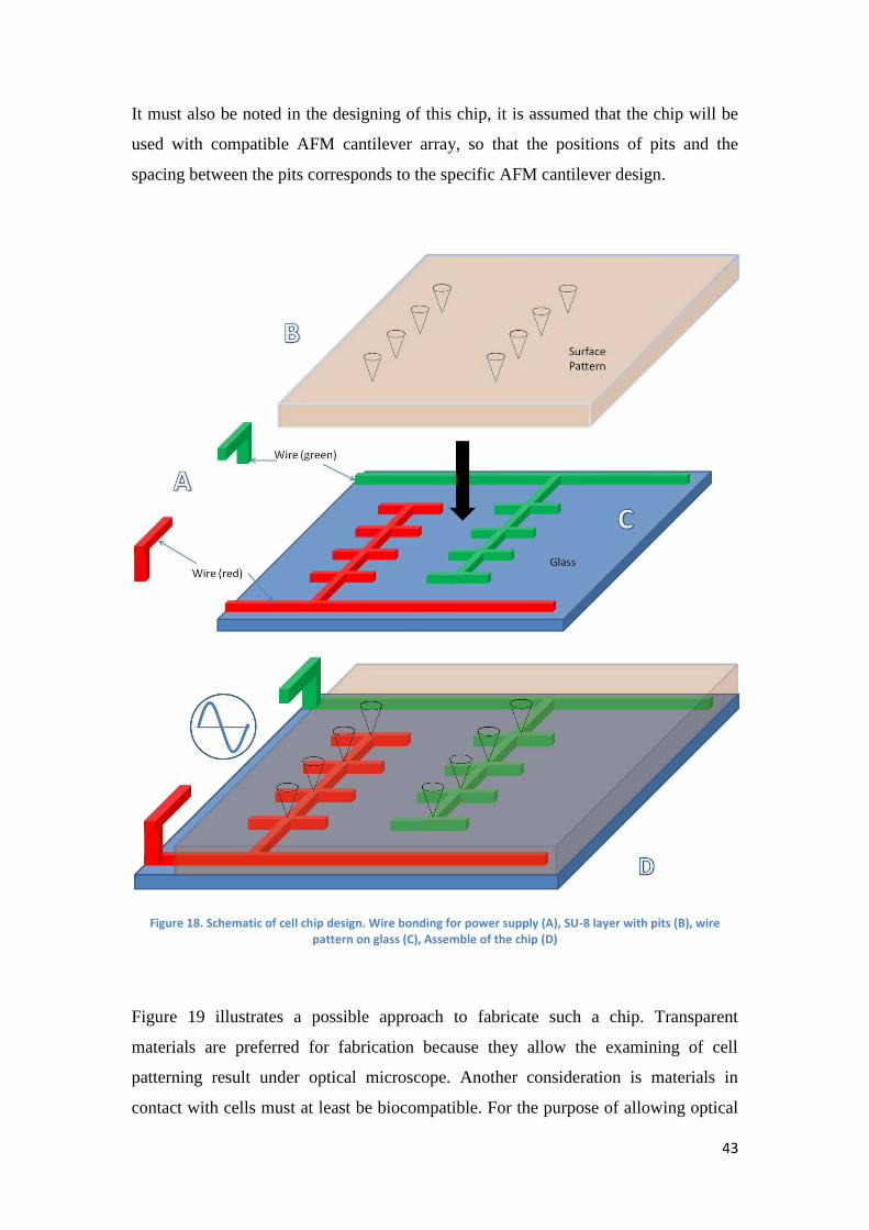
43
It must also be noted in the designing of this chip, it is assumed that the chip will be
used with compatible AFM cantilever array, so that the positions of pits and the
spacing between the pits corresponds to the specific AFM cantilever design.
Figure 18. Schematic of cell chip design. Wire bonding for power supply (A), SU-8 layer with pits (B), wire pattern on glass (C), Assemble of the chip (D)
Figure 19 illustrates a possible approach to fabricate such a chip. Transparent
materials are preferred for fabrication because they allow the examining of cell
patterning result under optical microscope. Another consideration is materials in
contact with cells must at least be biocompatible. For the purpose of allowing optical
44
examination, glass is chosen as a preferred substrate. Commercially available glass
wafer can be purchased with thickness ranging from 300 µm to 1 mm. for subsequent
fabrication, glass surface is cleaned with oxygen plasma first and a photo resist layer
is deposited by spin coating (B). After the photoresist has been cured, a photo mask
can be used to generate designed pattern for metal line deposition (C). Metal like
copper, gold and titanium can be deposited on glass by chemical vapour deposition
[142] (D), then a lift off process is used to produce the final pattern of metal wiring
(E). For creating the pit pattern, different biocompatible materials can be used. The
most commonly used biocompatible polymer in MEMS is PDMS, it is also
transparent. However, PDMS has a elastic modulus [143] that is very close to the
elastic modulus of cells, which can be as high as 200 kPa [59, 144]. Thus, probing cell
mechanical properties on PDMS may introduce error to the measurement. Other
materials can be used include PMMA and PS, However, both PMMA and PS need
contact printing to form the pits pattern, and additional adhesive (like epoxy) may
need to be applied between PMMA/PS and glass.
Figure 19. Fabrication process of cell chip

45
For the purpose of easy fabrication, SU-8 is chosen to be used to form the pit pattern.
SU-8 is biocompatible polymer that is commonly used as negative photoresist in UV
range [145-147]. SU-8 offers high elastic modulus after being cured up to 5 GPa [148,
149], sufficient for the purpose of cell mechanics testing. SU-8 is spin-coated on glass
substrate after the glass substrate is cleaned and dehydrated (F). The resist is baked
and then pressed under heating conditions for boding to glass wafer. The final step is
to expose SU-8 layer to a pit pattern printed on photo mask film to form the pit
pattern.
2.3 Integration and Control
With the design of AFM array and cell chip, the system can be integrated together. As
mentioned before, a modular design is preferred in order to lower down the
maintenance cost. So even if one module fails, it is possible to change that module
only without the need of replacing the whole set. A schematic component diagram of
the system is shown below. An array of four AFM sub arrays are shown on the graph,
they are integrated into one higher level array. The blue platform represents cell chip
mentioned in the previous part, while the area encircled under each cantilever array
shows the area probed by that array. The cell chip can be mounted on a piezo actuator
which can move the chip in 3 dimensions.
The signals pathways are shown in single line (input) and double line (output). The
signal processing system is modeled after commercially available controlling systems
from National Instrument®. Analogue signals can be read out by data acquisition
board (DAQ), which can also convert analogue input into digital signals. DAQ board
then send signals to I/O boards for interfacing with computer. Desired stimulation
form can be designed in computer and output to I/O board, which in turn control the
power source for actuating cantilever arrays. The data acquired by this control system
can be stored in the computer system for further analysis.

46
Figure 20. System component for high throughput cell force spectroscopy
For data analysis, fast Fourier transform can be carried out based on sampled force
data to generate complex modulus and phase angle [105]. Cells are modeled as
viscoelastic homogenous spherical balls indented with small and infinite hard indenter
[150]. Hertzian contact model and Maxwell-Weichert are coupled together for
dynamic modeling. Most AFM based systems use Hertzian contact model based on a
spherical tip to estimate the complex modulus of single cells. Revised Hertzian model
can be applied to account for different tip geometry [151]. The real part of the
complex modulus represents the storage of elastic energy, while the imaginary part
represents the loss of the energy. The relationship between complex modulus, force
and frequency are given by [105],
2
* 1 ( )| ( ) |
( )2spherical
o
F fE f
d fRd
where od is the indentation depth at 0 frequency, is the Poisson’s ratio and is
assumed to be 0.4 for chondrocytes [152], and is specific to cell phenotype. R is the
effective radius of contact.

47
A more accurate modeling of the force measurement takes into account of the
geometry of the tip, for a pyramidal tip,
2* 1 ( )
| ( ) |2 tan ( )
pyramidal
o
F fE f
d d f
Where tan defines the half angle of tip apex. The real part of the complex modulus
signifies the energy storage part of dynamic responses, while the imaginary part
signifies the energy loss part of dynamic responses corresponding to viscous flow.
Because of the utilization of continuum mechanics, the modeling of single cell
mechanics is relatively simplified. It ignored the inherited heterogeneous nature of
cell, which is composed of many microstructures. There have been experiments
showing that the stress distribution on a single cell is far from homogenous, and tends
to extend through cells [153] rather than to be localized as predicted by the models
based on homogenous models [53, 154, 155].
In the model of cell mechanics of tensegrity, the discrete nature has already been
taken into account. It has been demonstrated that the modelling of single cells as
tensegrity mimic a number of mechanical behaviors or properties of cells. For
example, this model predicts that the focal adhesion of cells will be accompanied by
the malleable deformation of cytoplasm and the nucleus will polarize and move
basally. This has been proved experimentally by the studying of living cells [156]. In
addition, it has been shown by time lapse video microscope observation that the
cytoskeleton network rearrange globally just as the tensegrity predicted [157]. The
experiments on the focal adhesion of cell to ECM also suggest cytoskeleton is a
tensegrity network because the compressional continuity was not observed in either
ECM or cytoskeleton [156].
It is thus interesting to seek further improvement on the accuracy of measurement
interpretation by incorporating tensegrity model in the mathematical modelling of
single cell mechanics. A few models [158, 159] have been devised to take into
account of tensegrity to model the dynamic responses of cells. By using these models,
the internal mechanical loadings on tensegrity elements like bars, which correspond to
microfilaments, and cables, which correspond to cytoplasm, can be derived from
external loadings; it may be useful to provide a way to directly estimate the
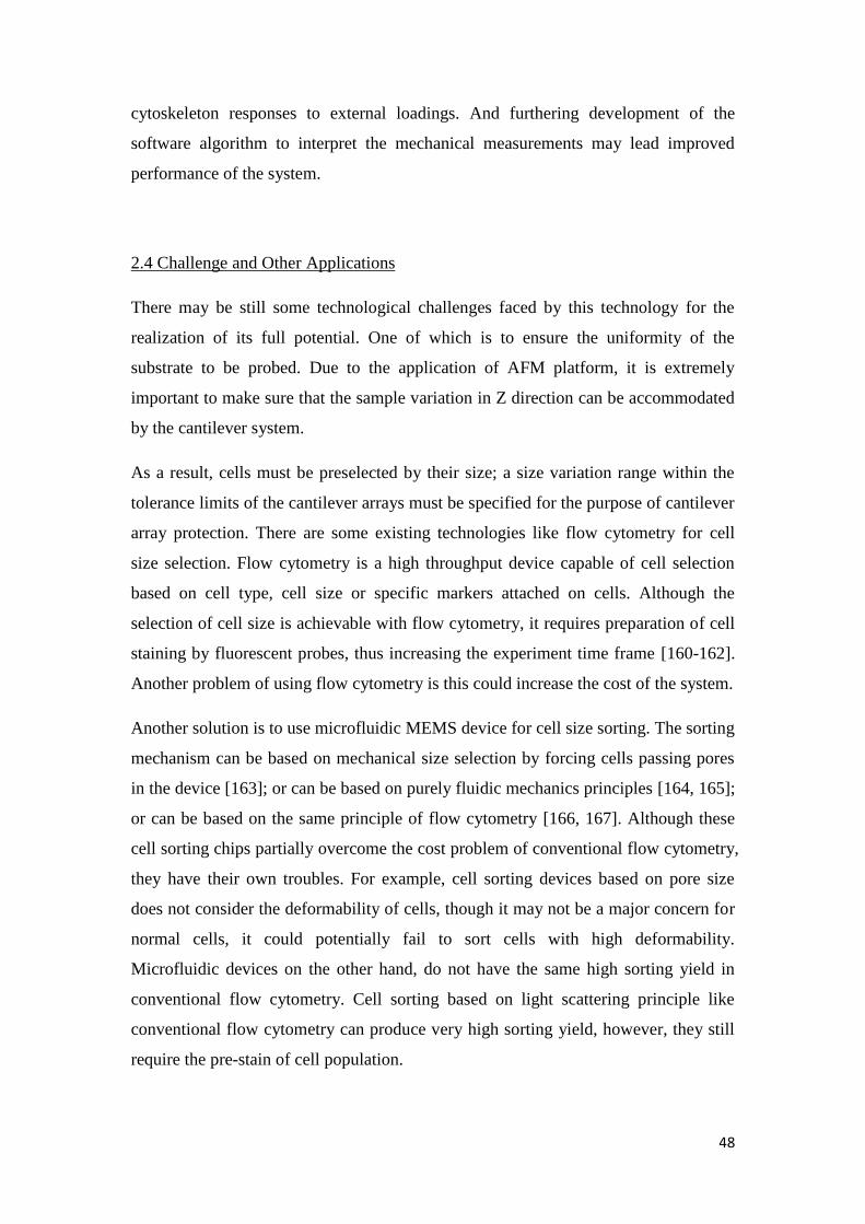
48
cytoskeleton responses to external loadings. And furthering development of the
software algorithm to interpret the mechanical measurements may lead improved
performance of the system.
2.4 Challenge and Other Applications
There may be still some technological challenges faced by this technology for the
realization of its full potential. One of which is to ensure the uniformity of the
substrate to be probed. Due to the application of AFM platform, it is extremely
important to make sure that the sample variation in Z direction can be accommodated
by the cantilever system.
As a result, cells must be preselected by their size; a size variation range within the
tolerance limits of the cantilever arrays must be specified for the purpose of cantilever
array protection. There are some existing technologies like flow cytometry for cell
size selection. Flow cytometry is a high throughput device capable of cell selection
based on cell type, cell size or specific markers attached on cells. Although the
selection of cell size is achievable with flow cytometry, it requires preparation of cell
staining by fluorescent probes, thus increasing the experiment time frame [160-162].
Another problem of using flow cytometry is this could increase the cost of the system.
Another solution is to use microfluidic MEMS device for cell size sorting. The sorting
mechanism can be based on mechanical size selection by forcing cells passing pores
in the device [163]; or can be based on purely fluidic mechanics principles [164, 165];
or can be based on the same principle of flow cytometry [166, 167]. Although these
cell sorting chips partially overcome the cost problem of conventional flow cytometry,
they have their own troubles. For example, cell sorting devices based on pore size
does not consider the deformability of cells, though it may not be a major concern for
normal cells, it could potentially fail to sort cells with high deformability.
Microfluidic devices on the other hand, do not have the same high sorting yield in
conventional flow cytometry. Cell sorting based on light scattering principle like
conventional flow cytometry can produce very high sorting yield, however, they still
require the pre-stain of cell population.

49
Although the concern of cell size variation can be alleviated by the use of cell sorting
devices, there is still deeper concern about the small size variation tolerance of AFM
array. Even if cell sorting does not require time consuming staining process, it may
still be a problem as only a fraction of cells can be selected from the total cell
population; this could cause huge waste, not only of the materials needed for cell
culture, but also of the cell source itself. This problem is more severe especially when
precious cells such as stem cells are used.
Another problem associated with the selection of the fraction of cell bears the
question whether this sub population could be a good enough sample to represent the
whole population of cells. Single cell mechanics may vary with cell size; so that
multiple batches of measurements have to be carried out for characterize the whole
population.
A fundamental solution to this problem is to fabricate AFM arrays with higher
tolerance. Less stiff materials [85, 168] could be used for the fabrication of array.
Future research would be needed to solve the problem.
The proposed system has good application potentials to a variety of tasks. Although
this technology platform is developed with the primary aim for high throughput
probing of single cell mechanics by the nanoindentation of AFM tips, it is possible to
modify this set up for other researches. With normal cell chip, cell response to
dynamic compression can be tested, with AFM tips functionalized with particles that
are large in size, whole cell mechanical property measurement can be obtained. If
chemical agents are used to functionalize cell chip for cell binding, the tensile
properties of single cells can also be tested.
AFM has found wide range of applications in pharmaceutical industries on molecular
basis. For example, by chemically modifying the tip of AFM, it is possible to detect
the binding forces between adhesive protein and the ligand of this protein on cell, thus
providing a quantitative assessment of protein-cell interaction. The same principle can
be applied in studying drug-cell interactions too [64]. In addition, due to the high
resolution provided by AFM, force measurement on molecular level is possible, there
are experiments performed on force measurement between single protein-ligand pair
[169], DNA double strands [170] and single molecule domains [171]. With current
design of the high throughput system, these molecules can be immobilized on
50
cantilever tips as well as in the pits, thus high throughput of single molecule
mechanics is possible.
Beyond the measurement of mechanical properties, there are other applications of
AFM in biological sciences; the flowing figure summarizes the application fields, and
many of them can be benefited with the development of the high-throughput AFM.
Figure 21. Possible applications of AFM technology in biology [172]
2.4.1 Beyond Biology
More applications of AFM can be found beyond the boundary of biological researches,
and the high throughput platform is also desirable in those applications. Active AFMs
with self actuations have been intensively researched in material science community
for the use on surface patterning. For example, AFM can be used to mechanically
patterning the polymer surface by indentation or plowing [96]. This was also the
original idea of IBM’s millipede, which performs thermal mechanical indentation for
51
data storage [173]. Another pattering technique biases cantilever tip with regards to
substrate surface. The oxidation is confined to the proximity of AFM tip, and it has
been demonstrated on silicon[174], III-V compound semiconductors, silicon carbide
and metal [175]. Furthermore, AFM arrays can be used to transfer molecules as ink on
to substrate surfaces [176], which is known as dip pen nanolithography (DPN) [177].
This technology can help to directly modify substrate surfaces and to fabricate ultra
thin mask on substrate, and is compatible with a wide variety of substrates, including
organic and biological materials [112].
However, the probe based surface patterning faces similar dilemma as probe based
single cell probing, as the low throughput of the device hinders the further adaption of
this technology. This high-throughput AFM cantilever array may find potential of
being applied in surface pattering as well. In fact, many researchers have already
begun to seek the application of array technology. For example, C.F.Quate in
Stanford University integrated four cantilever arrays, each consisting 50 cantilevers
for with independent control for each beam in local oxidation lithography [112].
52
Chapter 3 Commercialization
3.1 Intellectual Property
Intellectual property (IP) assessment is an important component to assess the
marketability of a new born technology. It can help to protect the IP of the new
technology and at the same time to avoid any confliction of IP interest with
established patent holders. The first part of this chapter focuses on the studying of
existing IPs
Patent searches were conducted to analyze IPs with two primary sources, namely,
Google Patent Search (www.google.com/patents) and the US Patent Office's
(www.uspto.gov)
There are numerous existing patents in the fabrication and application of cantilever
array as well as the cell chip. Most relevant patents about the fabrication process have
already expired so that no cost is incurred by applying these technologies in the
fabrication process. For example, to fabricate the AFM array and the cell chip, Sol-gel
deposition, sputtering, photolithography and CVD are needed, the patents about sol
gel deposition of PZT materials with spin coating were filed since 1989 [178], the
earliest patent about photolithography using SU-8 dates back to 1974, and the most
relevant one was filed by IBM in 1989 [179]. The sputtering deposition was file
before 1950 [180] and CVD of metal was filed back to 1980s [181].
There are about 390 patents regarding the technology field of arrayed AFM filed
between 1988 and 2010, suggesting this is a rather interesting research territory.
These patents mostly use different design of cantilever systems, for example, the
patent for multiple probe measurement uses mechanically coupled probes for testing
[182]. Furthermore, many patents of multiple cantilevers centre around concept such
as data storage [183]. The most relevant patents in this category are Atomic force
microscope for biological specimens [184] and Tapping atomic force microscope
[185]. These patents are about the applications of a single probe. There are about 80
patents regarding the application of arrayed AFM to biological study, however, most

53
of these patents concern about biomolecules testing. No patent exists about the
application of AFM array for single cell mechanics testing.
There are 127 patents about cell chip for cell positioning. There are patents about cell
positioning with mechanical means [186] as well as with dielectrophoresis means
[187]. However, no patent was found to combine both techniques.
The patterns of the filed patents in related fields indicate that this high throughput
device is entering a technology territory that is less explored. This new technology
introduces novel applications of AFM arrays testing single cell mechanics with a
novel cell chip design; the salient features of this system are not yet patented. In
summary, no severe barriers for the new technology were found and the technology
should be patentable.
In summary, the technology platform represents a collection of novelties which
should be patentable in the following areas:
a) Design and manufacturing procedures of piezo AFM arrays
b) Design and manufacturing procedures of cell chip for cell positioning
c) Application of piezo AFM array and cell chip for single cell mechanics testing
d) Measurement and controlling algorithms
However, it must be noted that there are a range of patents and publications in area a)
already, it is most advisable to improve on the current design and manufacturing
processes before the patents are files.
3.2 Market
With the study of single cell mechanics gaining more attention, devices for quantify
single cell mechanical properties will face a growing demand. In addition,
pharmaceutical companies and administrative agencies involved in the developing
tissue engineering products need a tool that can assess the mechanical properties of
cells from engineered tissue. Other potential applications are also accessible by some
slight modification of this platform. Presently, there is no commercially available
solution which is of high efficiency and in the meantime is a potentially multitask
platform. The cantilever array based cell force microscope is designed to fulfil this

54
void by targeting at this high demand, price inelastic market. Great market
opportunity could be expected for this product.
The market analysis of AFM with arrayed cantilevers is based on evaluations of
current market for AFM and a case study. The data of AFM market research was
drawn from ITRS, Frost & Sullivan [188, 189]. The material for case study was
drawn from the financial report form 10K of the leading company (Veeco) in AFM
market. It is also noted that the market research typically group AFM with closely
related technology and products of Surface Tunnelling Microscope (STM) and Near
Field Scanning Optical Microscope (NSOM).
The primary source for AFM market data is from World Microscopes Markets [189].
The AFM market was estimated about 572.3 million in 2008 [190], with a projected
growth rate of 15.3% annually till 2013. The competition structure of the market
comprises three tiers. The first tier is occupied by large companies like Veeco and
JEOL, which offer whole range of product line and have a broad installation base. The
second tier comprises smaller companies like Park System and JPK Instruments,
which are typically privately owned, and exploit niche market. The third tier
comprises companies produce various AFM accessories. The market strategy for our
start up company is to enter second tier first, because small scale production can help
the start up company to reduce the need for huge initial investment, and in the mean
time to concentrate to the specialization it possesses. Further expansion to first tier is
desired after the first phase of market entering is successful.
The key end user group of the market is segmented into general industry, including
semiconductor industry, electronics industry and materials industry, biomedical
companies and research institutions/universities. Among all customers, biomedical
companies and research institutions hold about 50% of market share, which is the
primary target of the proposed technology platform. The gross margin of AFM
products is typically about 40% [191], which is also high enough to motivate large
initial investment and subsequent R & D.
AFM market exists globally, the market with Asian pacific as the number one market
which holds about 50% of market value. North America and EU hold the second and
the third place.
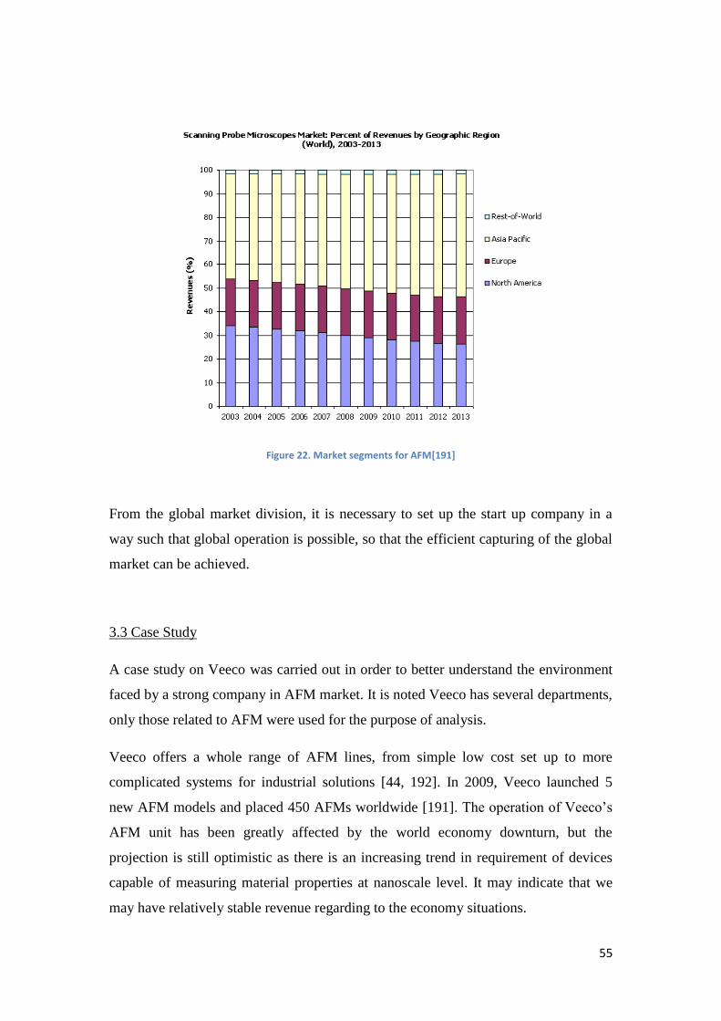
55
Figure 22. Market segments for AFM[191]
From the global market division, it is necessary to set up the start up company in a
way such that global operation is possible, so that the efficient capturing of the global
market can be achieved.
3.3 Case Study
A case study on Veeco was carried out in order to better understand the environment
faced by a strong company in AFM market. It is noted Veeco has several departments,
only those related to AFM were used for the purpose of analysis.
Veeco offers a whole range of AFM lines, from simple low cost set up to more
complicated systems for industrial solutions [44, 192]. In 2009, Veeco launched 5
new AFM models and placed 450 AFMs worldwide [191]. The operation of Veeco’s
AFM unit has been greatly affected by the world economy downturn, but the
projection is still optimistic as there is an increasing trend in requirement of devices
capable of measuring material properties at nanoscale level. It may indicate that we
may have relatively stable revenue regarding to the economy situations.

56
The sales of metrology product consists of about 30% of total net sales of Veeco, and
the gross profit (40%) remains flat despite the economy situation. The majority of
sales and procurement of Veeco relies primarily on several partners, which may
impose risks on the supply chain.
Veeco spent about 15% of revenue in research and development; this may be due to
the high speed of technological evolution. We recognize it is necessary for us to
invest in R&D too if we want to keep up with competition.
In terms of revenue realization, AFM customers generally require no substantial
provisional period and the installation is insignificant. As such, revenue is realized
soon after the device is shipped. It may be beneficial for a start up company to
minimize inventory cost and maximize cash flow.
3.4 Business Strategy
For the realization of the high-throughput AFM, two approaches may be preceded.
The first approach is to align with existing market players, by utilizing the intellectual
property to gain profit. The other approach would be set up a company to produce the
technology platform. From the market analysis above, it is clear that the market is
growth is rather strong in AFM sector, and the market capacity is large enough to hold
both large and smaller companies. In this market, smaller companies may excel in
certain areas by providing specific product to tailor the needs of specific customer,
because the market provides a high profit margin for the device manufacturer. In
addition, due to the protection of IP, these specific markets is not likely to be engulfed
by the larger companies if the smaller companies are able to hold a comprehensive
collection of patents. Meanwhile, profit generation from IP could not provide a gross
margin as high as producing the product by one’s own, since in the profit chain model,
a company producing the product will be able to reap margins from the bottom of the
chain, which is R & D, until top of the chain, which are final product sales. Moreover,
this technology break through has potentials to be applied in various fields in research
and industry as illustrated in previous section; this represent a great opportunity for a
company holding this technology to expand into various market. In summary of all
above considerations, it is more likely that to build a start up company will eventually
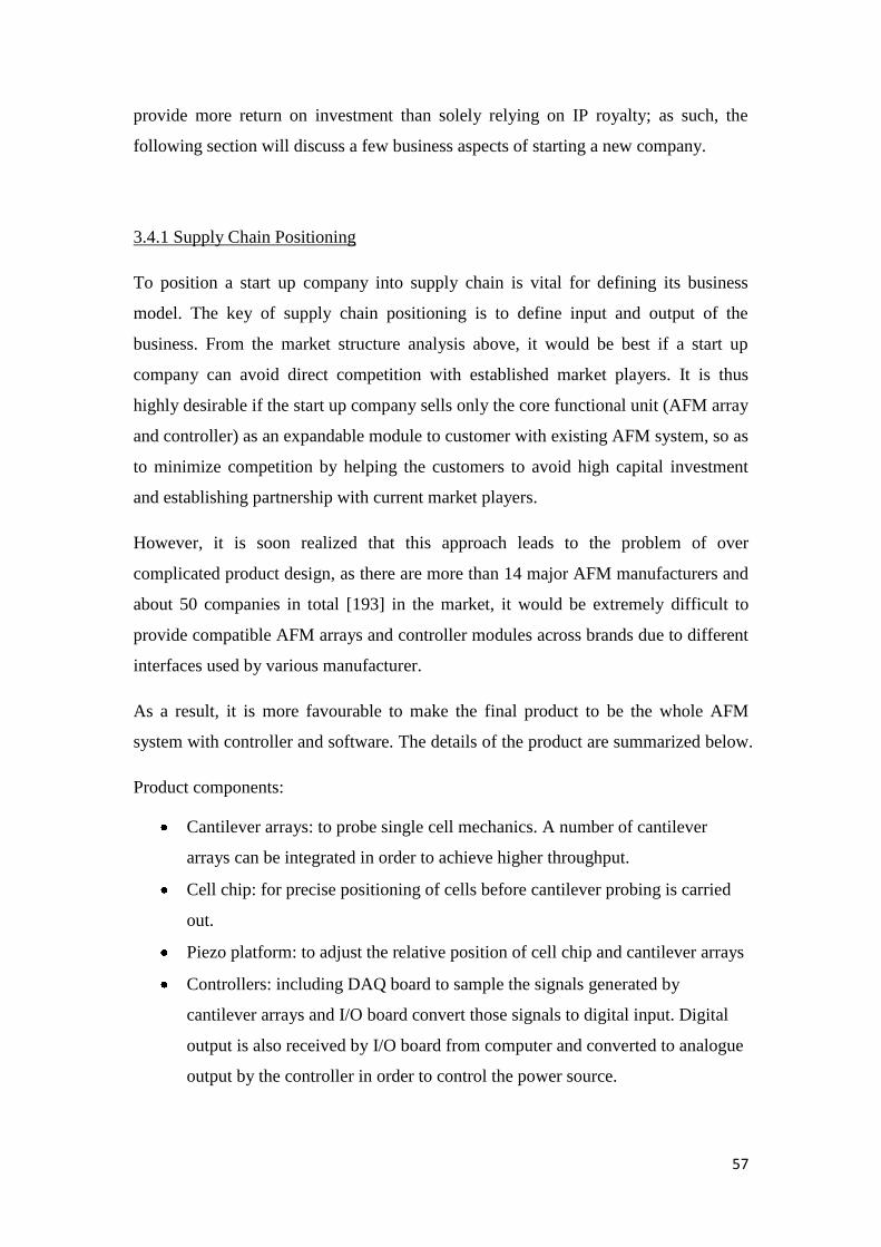
57
provide more return on investment than solely relying on IP royalty; as such, the
following section will discuss a few business aspects of starting a new company.
3.4.1 Supply Chain Positioning
To position a start up company into supply chain is vital for defining its business
model. The key of supply chain positioning is to define input and output of the
business. From the market structure analysis above, it would be best if a start up
company can avoid direct competition with established market players. It is thus
highly desirable if the start up company sells only the core functional unit (AFM array
and controller) as an expandable module to customer with existing AFM system, so as
to minimize competition by helping the customers to avoid high capital investment
and establishing partnership with current market players.
However, it is soon realized that this approach leads to the problem of over
complicated product design, as there are more than 14 major AFM manufacturers and
about 50 companies in total [193] in the market, it would be extremely difficult to
provide compatible AFM arrays and controller modules across brands due to different
interfaces used by various manufacturer.
As a result, it is more favourable to make the final product to be the whole AFM
system with controller and software. The details of the product are summarized below.
Product components:
Cantilever arrays: to probe single cell mechanics. A number of cantilever
arrays can be integrated in order to achieve higher throughput.
Cell chip: for precise positioning of cells before cantilever probing is carried
out.
Piezo platform: to adjust the relative position of cell chip and cantilever arrays
Controllers: including DAQ board to sample the signals generated by
cantilever arrays and I/O board convert those signals to digital input. Digital
output is also received by I/O board from computer and converted to analogue
output by the controller in order to control the power source.

58
Software: software modulus for controlling the hardware and for interpreting
the acquired data
Power source
Companies producing AFM instruments seek to play in more than one sector for
healthy business growth. The start up company will enter the rapidly developing
industry as a device fabrication enterprise with strong technology and development
background.
Figure 23. Supply chain of start up company
The supply chain for the start up company is illustrated in above figure. There are
three subsectors in the supply chain, namely, the supplier side which in charge of
providing raw materials and the controller modules; the start up company which is
responsible for manufacturing of the cantilever array and cell chip, the design of the
controlling algorithms and analysis software and R&D for product development; and
distribution channel, which is responsible for providing customers with the final
product. The fabrication of the controller circuits can be outsourced to more
experienced companies who are in possess of required tools and are specialized in
fabrication of chips the in order to decrease the investment and reduce cost. Several
important factors have to be considered for the building of the supply chain:
To secure the timely delivery of high quality raw materials
Suppliers
•Raw Materials
•Controller
Start up company
•Manufacturing
•R&D
•Design Controller
•Sales & Marketing
•service
Distribution
•Products
•Software
•Accessory

59
To ensure timely delivery of products to customers by partnering with
established distributors
To build up a competitive price for product with technological edge
3.4.2 Cost Modelling
The cost assessment is conducted based on the estimations of fixed cost and variable
cost. The cost figure could provide a guide on the continual optimization in cost,
reliability and fabrication technique in the future. The actual cost analysis should be
done in more details and consider more factors.
Two approaches were used for cost modelling. It is worth noticing that only crude
estimation can be made before the actual process of production.
The fixed cost was estimated with a top-down approach with data gathered from
Veeco’s financial report. A total of 16.6 million worth equipments, plants and
properties has been acquired by Veeco for the production of AFM, and there annual
production is 450 AFMs.
To estimate the fixed cost of the new start up, an evaluation of annual production
target has to be devised first. Assuming we can produce 90 AFMs per year, a very
rough approximation of the total fixed cost would be 3.32 million. The fixed cost is
then spread out over the production period of AFM device, so if it is assumed that a
linear relationship exists between production volume and the fixed cost, the average
fixed cost can be calculated from the production lifetime.
The core fabrication process of this device is the production of AFM array and cell
chip. The cost model is based on laboratory techniques for producing the system, the
dimensions of materials used are estimated from literatures [99, 138-141]. However, it
is worth noticing that this is also a rough estimation only since the cost in laboratory
settings does not always reflect the cost in mass production.
The cost of materials and processes were obtained from various sources [194-207],
CES Edupack ® was also used to facilitate the estimation of cost and processing. The
variable cost was estimated to be 960 USD per array, with labour cost being the single

60
largest cost for device fabrication (52%). More detailed production cost breakdown
can be referred to Appendix B.
Figure 24. Variable cost modelling for Piezo deposition and SU-8 coating
The variable cost of the chip production is based on the estimation of chip size. An
estimation of 1cm ×1cm is used; cost of producing chips with different size doesn’t
vary dramatically with the size of chip, as size dependent component (material cost)
only account for 27% of the total cost. Among the material cost, the cost of
photoresist is almost negligible. For batch fabrication, labour cost can be averaged out
2% 3%
52%
4%
26%
13%
Variable cost in array fabrication
wafer
Other materials in Sol Gel
labour in Sol Gel
energy in Sol Gel
Pre Sol Gel masking
Pre Sol Gel etching
0%
14%
6%
7%
73%
Variable cost in chip fabrication
photo resist
metal
glass wafer
energy
labour
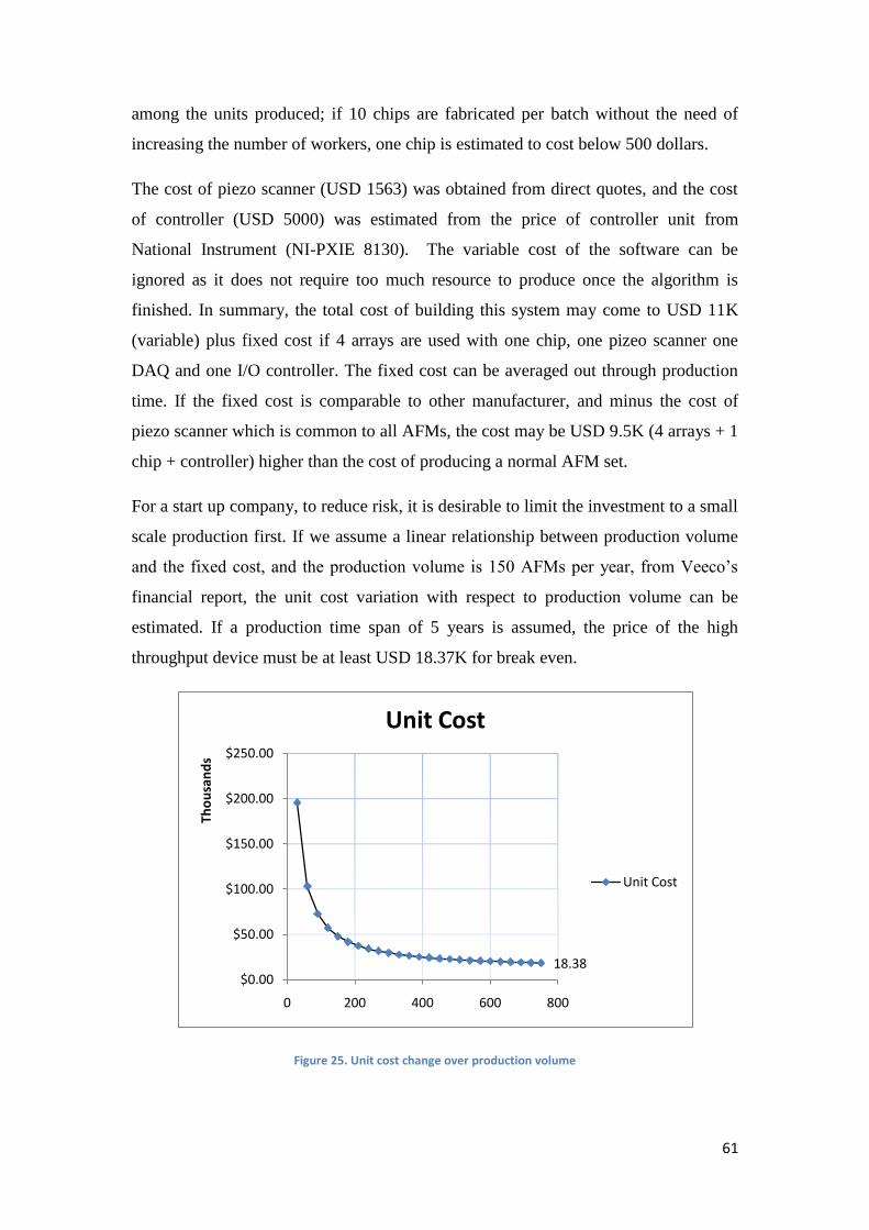
61
among the units produced; if 10 chips are fabricated per batch without the need of
increasing the number of workers, one chip is estimated to cost below 500 dollars.
The cost of piezo scanner (USD 1563) was obtained from direct quotes, and the cost
of controller (USD 5000) was estimated from the price of controller unit from
National Instrument (NI-PXIE 8130). The variable cost of the software can be
ignored as it does not require too much resource to produce once the algorithm is
finished. In summary, the total cost of building this system may come to USD 11K
(variable) plus fixed cost if 4 arrays are used with one chip, one pizeo scanner one
DAQ and one I/O controller. The fixed cost can be averaged out through production
time. If the fixed cost is comparable to other manufacturer, and minus the cost of
piezo scanner which is common to all AFMs, the cost may be USD 9.5K (4 arrays + 1
chip + controller) higher than the cost of producing a normal AFM set.
For a start up company, to reduce risk, it is desirable to limit the investment to a small
scale production first. If we assume a linear relationship between production volume
and the fixed cost, and the production volume is 150 AFMs per year, from Veeco’s
financial report, the unit cost variation with respect to production volume can be
estimated. If a production time span of 5 years is assumed, the price of the high
throughput device must be at least USD 18.37K for break even.
Figure 25. Unit cost change over production volume
18.38$0.00
$50.00
$100.00
$150.00
$200.00
$250.00
0 200 400 600 800
Tho
usa
nd
s
Unit Cost
Unit Cost
62
3.4.3 Utility and Feasibility Analysis
From the product cost point of view, the device may cost up to USD 9.5K more than
average AFM cost. Thus there could be some doubt whether this product would be
accepeted by the targeted market. Average AFM cost about USD 15K to 40K depends
on the complexity, if the targeted market is the high end AFM users, the high
througput device may cost 25% more than convnetional technology.
The major limitation of AFM is the low throughput problem. There is currently no
competing technologies available in the market offering the same degree of
automation, resolution and throughput in a single product. If four AFM cantilever
arrays are supplied in one pacakge, each array consists 50 cantilevers as used by
Quate [112], the throughput will be 200 times of the throughput of a single probe
AFM. Thus the benefit is quite likely to be more than the cost increase.
Through the case study, it is found AFM profit can be as high as 40%, and can remain
flat even in economy down turn. It is possible for the start up company to lower down
the gross margin in the first place to capture the market.Through the market analysis,
it is clear that AFM market is expanding at a rate about 15% per year, and AFM for
biomechanical research represents a major contibution of the market expansion.
Moreover, this high-throughput device has the potential to be a multitask platform so
its potential application is not just limited by the filed biomechanical research. The
market expandablity for the start up company could be high due to both market
expansion as well as technology branching out.
There are also various ways for lowering down the cost. Considering the major
variable cost is down to the controller units, it is possible that the cost of the product
can be lowered by establishing direct partnership with controller providers. Other cost
reducing methods may include the optimization of fabrication processes and the
renting of equipement, plant instead of purchasing.
63
Chapter 4 Conclusion
Single cell mechanics has emerged as an important branch in the studying cell biology.
Although research has been focused on the characterization of single cell mechanical
properties based on a small population of cells, it is recognized this approach cannot
truly account the complexity of heterogeneous cell population in most living
organisms. Thus for the purpose of quantitative assessment of a large population of
cell, a force measurement device with high resolution and high throughput is
necessary.
The first part of thesis is concentrated on the biological back ground which connects
single cell mechanics to various cellular activities. A deep correlation between single
cell mechanic properties and cytoskeletal structures was explained, the application of
single cell mechanics was shown including the characterization of cells and
identification diseases.
In the second part, a system composited novel AFM cantilever array and cell is
proposed and studied. Different AFM cantilever array technology and cell chip
technology are compared and suitable technology was chosen for the fabrication of
the device. It is found that the fabrication of the device does not contribute much
difficulty for the realization of the technology. Although the technology may still face
some challenge to realize its full potential, these challenges are not fatal for the
technolgy and they can be overcome by the use of additional device or the advacne of
complementary technologies, such as cell sorting chip.
Feasibility study based on commercialization of the concepts was also carried out,
through the analysis of intellectual property; it is shown that this technology would be
patentable as it combines novel features of both AFM patents and cell chip patents.
Market analysis was also carried out to assess environment faced by companies in this
sector. Through the analysis of business strategy, the author found strong market
growth and good IP protection could facilitate the start up and the expansion of the
company, meanwhile to set up a start up company for producing such technology
platform may generate more return for investment. As a result, it seems more

64
profitable to realize the technology through joining the device fabrication industry
rather than through the collecting IP royalties. Although the fabrication cost was
would be higher for such a system compared to common AFM, it is possible that the
utilities provided by this technology overweighs its expenses. Further cost reduction
may come from the expansion in production scale and advancing in manufacturing
processes.
In conclusion, this technology represents advancement in the development force
measuring devices, because no competing device with equivalent precision and
throughput is offered in current market, this technology can receive positive market
responses.

65
References
[1] P. A. Janmey, "The cytoskeleton and cell signaling: Component localization and mechanical coupling," Physiological Reviews, vol. 78, pp. 763-781, 1998.
[2] K. Burridge, K. Fath, T. Kelly, G. Nuckolls, and C. Turner, "Focal adhesions: Transmembrane junctions between the extracellular matrix and the cytoskeleton," Annual Review of Cell Biology, vol. 4, pp. 487-525, 1988.
[3] T. DW, On Growth and Form, 2 ed. London: Cambridge University Press, 1952. [4] D. Ingber, "Integrins as mechanochemical transducers," Current Opinion in Cell
Biology, vol. 3, pp. 841-848, 1991. [5] C. M. Cuerrier, M. Benoit, G. Guillemette, F. Gobeil Jr, and M. Grandbois, "Real-time
monitoring of angiotensin II-induced contractile response and cytoskeleton remodeling in individual cells by atomic force microscopy," Pflugers Archiv European Journal of Physiology, vol. 457, pp. 1361-1372, 2009.
[6] R. Sunyer, X. Trepat, J. J. Fredberg, R. Farre, and D. Navajas, "The temperature dependence of cell mechanics measured by atomic force microscopy," Physical Biology, vol. 6, 2009.
[7] B. Lee, "Time-dependent mechanical behavior of newly developing matrix of bovine primary chondrocytes and bone marrow stromal cells using Atomic Force Microscopy," in Department of Materials Science and Engineering. vol. Doctor of Philosophy Cambridge: Massachussets Institute of Technology, 2009, p. 189.
[8] J. Alcaraz, L. Buscemi, M. Grabulosa, X. Trepat, B. Fabry, R. Farr 茅, and D. Navajas,
"Microrheology of human lung epithelial cells measured by atomic force microscopy," Biophysical Journal, vol. 84, pp. 2071-2079, 2003.
[9] K. J. Van Vliet, G. Bao, and S. Suresh, "The biomechanics toolbox: Experimental approaches for living cells and biomolecules," Acta Materialia, vol. 51, pp. 5881-5905, 2003.
[10] E. M. Darling, M. Topel, S. Zauscher, T. P. Vail, and F. Guilak, "Viscoelastic properties of human mesenchymally-derived stem cells and primary osteoblasts, chondrocytes, and adipocytes," Journal of Biomechanics, vol. 41, pp. 454-464, 2008.
[11] C. Rotsch, K. Jacobson, and M. Radmacher, "Dimensional and mechanical dynamics of active and stable edges in motile fibroblasts investigated by using atomic force microscopy," Proceedings of the National Academy of Sciences of the United States of America, vol. 96, pp. 921-926, 1999.
[12] T. P. Stossel, "The machinery of cell crawling," Scientific American, vol. 271, pp. 54-55, 58, 1994.
[13] J. Bereiter-Hahn, "Mechanics of crawling cells," Medical Engineering and Physics, vol. 27, pp. 743-753, 2005.
[14] S. Tavella, P. Raffo, C. Tacchetti, R. Cancedda, and P. Castagnola, "N-CAM and N-cadherin expression during in vitro chondrogenesis," Experimental Cell Research, vol. 215, pp. 354-362, 1994.
[15] J. Durr, S. Goodman, A. Potocnik, H. Von Der Mark, and K. Von Der Mark, "Localization of beta1-integrins in human cartilage and their role in chondrocyte adhesion to collagen and fibronectin," Experimental Cell Research, vol. 207, pp. 235-244, 1993.
[16] T. Ochalek, F. J. Nordt, K. Tullberg, and M. M. Burger, "Correlation between cell deformability and metastatic potential in B16-F1 melanoma cell variants," Cancer Research, vol. 48, pp. 5124-5128, 1988.
[17] A. Moustakas and C. Stournaras, "Regulation of actin organisation by TGF-beta in H-ras-transformed fibroblasts," Journal of Cell Science, vol. 112, pp. 1169-1179, 1999.
66
[18] C. C. Cunningham, J. B. Gorlin, D. J. Kwiatkowski, J. H. Hartwig, P. A. Janmey, H. R. Byers, and T. P. Stossel, "Actin-binding protein requirement for cortical stability and efficient locomotion," Science, vol. 255, pp. 325-327, 1992.
[19] K. M. K. Rao and H. J. Cohen, "Actin cytoskeletal network in aging and cancer," Mutation Research - DNAging Genetic Instability and Aging, vol. 256, pp. 139-148, 1991.
[20] S. Suresh, J. Spatz, J. P. Mills, A. Micoulet, M. Dao, C. T. Lim, M. Beil, and T. Seufferlein, "Connections between single-cell biomechanics and human disease states: Gastrointestinal cancer and malaria," Acta Biomaterialia, vol. 1, pp. 15-30, 2005.
[21] J. Noritake, M. Fukata, K. Sato, M. Nakagawa, T. Watanabe, N. Izumi, S. Wang, Y. Fukata, and K. Kaibuchi, "Positive Role of IQGAP1, an Effector of Rac1, in Actin-Meshwork Formation at Sites of Cell-Cell Contact," Molecular Biology of the Cell, vol. 15, pp. 1065-1076, 2004.
[22] D. E. Ingber, "Mechanobiology and diseases of mechanotransduction," Annals of Medicine, vol. 35, pp. 564-577, 2003.
[23] J. S. Clegg, "Intracellular water and the cytomatrix: Some methods of study and current views," Journal of Cell Biology, vol. 99, 1984.
[24] S. Kaech, L. Covic, A. Wyss, and K. Ballmer-Hofer, "Association of p60(c-src) with polyoma virus middle-T antigen abrogating mitosis-specific activation," Nature, vol. 350, pp. 431-433, 1991.
[25] P. D. Zalewski, L. J. Forbes, C. Giannikis, and W. H. Betts, "Regulation of protein kinase C by Zn2+-dependent interaction with actin," Biochemistry International, vol. 24, pp. 1103-1110, 1991.
[26] S. Akiba, T. Sato, and T. Fujii, "Evidence for an increase in the association of cytosolic phospholipase A2 with the cytoskeleton of stimulated rabbit platelets," Journal of Biochemistry, vol. 113, pp. 4-6, 1993.
[27] T. A. Kalfa, S. Pushkaran, N. Mohandas, J. H. Hartwig, V. M. Fowler, J. F. Johnson, C. H. Joiner, D. A. Williams, and Y. Zheng, "Rac GTPases regulate the morphology and deformability of the erythrocyte cytoskeleton," Blood, vol. 108, pp. 3637-3645, 2006.
[28] M. Mazzanti, R. Assandri, A. Ferroni, and D. Difrancesco, "Cytoskeletal control of rectification and expression of four substates in cardiac inward rectifier K<sup>+</sup> channels," FASEB Journal, vol. 10, pp. 357-361, 1996.
[29] B. D. Johnson and L. Byerly, "Ca2+ channel Ca2+-dependent inactivation in a mammalian central neuron involves the cytoskeleton," Pflugers Archiv European Journal of Physiology, vol. 429, pp. 14-21, 1994.
[30] H. Denk and E. Lackinger, "Cytoskeleton in liver diseases," Seminars in Liver Disease, vol. 6, pp. 199-211, 1986.
[31] K. Zatloukal, C. Stumptner, A. Fuchsbichler, P. Fickert, C. Lackner, M. Trauner, and H. Denk, "The keratin cytoskeleton in liver diseases," Journal of Pathology, vol. 204, pp. 367-376, 2004.
[32] R. J. Pei, N. Danbara, M. Tsujita-Kyutoku, T. Yuri, and A. Tsubura, "Immunohistochemical profiles of Mallory body by a panel of anti-cytokeratin antibodies," Medical Electron Microscopy, vol. 37, pp. 114-118, 2004.
[33] V. T. Ludwig J, "Non-alcoholic steatohepatitis. Mayo Clinic experiences with a hitherto unnamed disease," Mayo Clin Proc, vol. 55, pp. 434-438, 1980.
[34] N. Suarez-Huerta, R. Mosselmans, J. E. Dumont, and B. Robaye, "Actin depolymerization and polymerization are required during apoptosis in endothelial cells," Journal of Cellular Physiology, vol. 184, pp. 239-245, 2000.

67
[35] M. G. Levee, M. I. Dabrowska, J. L. Lelli Jr, and D. B. Hinshaw, "Actin polymerization and depolymerization during apoptosis in HL-60 cells," American Journal of Physiology - Cell Physiology, vol. 271, 1996.
[36] S. M. Laster and J. M. Mackenzie Jr, "Bleb formation and F-actin distribution during mitosis and tumor necrosis factor-induced apoptosis," Microscopy Research and Technique, vol. 34, pp. 272-280, 1996.
[37] M. Van Engeland, H. J. H. Kuijpers, F. C. S. Ramaekers, C. P. M. Reutelingsperger, and B. Schutte, "Plasma membrane alterations and cytoskeletal changes in apoptosis," Experimental Cell Research, vol. 235, pp. 421-430, 1997.
[38] M. J. Rosenbluth, W. A. Lam, and D. A. Fletcher, "Analyzing cell mechanics in hematologic diseases with microfluidic biophysical flow cytometry," Lab on a Chip - Miniaturisation for Chemistry and Biology, vol. 8, pp. 1062-1070, 2008.
[39] L. A. Durrant, C. W. Archer, M. Benjamin, and J. R. Ralphs, "Organisation of the chondrocyte cytoskeleton and its response to changing mechanical conditions in organ culture," Journal of Anatomy, vol. 194, pp. 343-353, 1999.
[40] D. E. Ingber, L. Dike, L. Hansen, S. Karp, H. Liley, A. Maniotis, H. McNamee, D. Mooney, G. Plopper, J. Sims, and N. Wang, "Cellular tensegrity: Exploring how mechanical changes in the cytoskeleton regulate cell growth, migration, and tissue pattern during morphogenesis," International Review of Cytology, vol. 150, pp. 173-224, 1994.
[41] D. E. Ingber, "Tensegrity: The architectural basis of cellular mechanotransduction," in Annual Review of Physiology. vol. 59, 1997, pp. 575-599.
[42] T. A. McMahon, Muscles, Reflexes, and Locomotion. N.J: Princeton Univ. Press, 1984. [43] P. Canadas, V. M. Laurent, C. Oddou, D. Isabey, and S. Wendling, "A cellular
tensegrity model to analyse the structural viscoelasticity of the cytoskeleton," Journal of Theoretical Biology, vol. 218, pp. 155-173, 2002.
[44] K. S. Zaner and P. A. Valberg, "Viscoelasticity of F-actin measured with magnetic microparticles," Journal of Cell Biology, vol. 109, pp. 2233-2243, 1989.
[45] J. R. Sims, S. Karp, and D. E. Ingber, "Altering the cellular mechanical force balance results in integrated changes in cell, cytoskeletal and nuclear shape," Journal of Cell Science, vol. 103, pp. 1215-1222, 1992.
[46] W. A, "Actin-binding proteins," Nature, p. 6, 1982. [47] R. Zhang and F. L. H. Brown, "Cytoskeleton mediated effective elastic properties of
model red blood cell membranes," Journal of Chemical Physics, vol. 129, 2008. [48] H. W. G. Lim, M. Wortis, and R. Mukhopadhyay, "Stomatocyte-discocyte-echinocyte
sequence of the human red blood cell: Evidence for the bilayer-couple hypothesis from membrane mechanics," Proceedings of the National Academy of Sciences of the United States of America, vol. 99, pp. 16766-16769, 2002.
[49] W. R. Trickey, T. P. Vail, and F. Guilak, "The role of the cytoskeleton in the viscoelastic properties of human articular chondrocytes," Journal of Orthopaedic Research, vol. 22, pp. 131-139, 2004.
[50] G. W. Schmid-Schonbein, K. L. P. Sung, and H. Tozeren, "Passive mechanical properties of human leukocytes," Biophysical Journal, vol. 36, pp. 243-256, 1981.
[51] W. R. Trickey, F. P. T. Baaijens, T. A. Laursen, L. G. Alexopoulos, and F. Guilak, "Determination of the Poisson's ratio of the cell: Recovery properties of chondrocytes after release from complete micropipette aspiration," Journal of Biomechanics, vol. 39, pp. 78-87, 2006.
[52] E. Evans and A. Yeung, "Apparent viscosity and cortical tension of blood granulocytes determined by micropipet aspiration," Biophysical Journal, vol. 56, pp. 151-160, 1989.

68
[53] A. R. Bausch, F. Ziemann, A. A. Boulbitch, K. Jacobson, and E. Sackmann, "Local measurements of viscoelastic parameters of adherent cell surfaces by magnetic bead microrheometry," Biophysical Journal, vol. 75, pp. 2038-2049, 1998.
[54] B. Fabry, G. N. Maksym, J. P. Butler, M. Glogauer, D. Navajas, and J. J. Fredberg, "Scaling the microrheology of living cells," Physical Review Letters, vol. 87, 2001.
[55] J. Sleep, D. Wilson, R. Simmons, and W. Gratzer, "Elasticity of the red cell membrane and its relation to hemolytic disorders: An optical tweezers study," Biophysical Journal, vol. 77, pp. 3085-3095, 1999.
[56] Y. Wang, E. L. Botvinick, Y. Zhao, M. W. Berns, S. Usami, R. Y. Tsien, and S. Chien, "Visualizing the mechanical activation of Src," Nature, vol. 434, pp. 1040-1045, 2005.
[57] P. G. Chao, Z. Tang, E. Angelini, A. C. West, K. D. Costa, and C. T. Hung, "Dynamic osmotic loading of chondrocytes using a novel microfluidic device," Journal of Biomechanics, vol. 38, pp. 1273-1281, 2005.
[58] F. Guilak, G. R. Erickson, and H. P. Ting-Beall, "The effects of osmotic stress on the viscoelastic and physical properties of articular chondrocytes," Biophysical Journal, vol. 82, pp. 720-727, 2002.
[59] G. Bao and S. Suresh, "Cell and molecular mechanics of biological materials," Nature Materials, vol. 2, pp. 715-725, 2003.
[60] N. Desprat, A. Richert, J. Simeon, and A. Asnacios, "Creep function of a single living cell," Biophysical Journal, vol. 88, pp. 2224-2233, 2005.
[61] J. P. Shelby, J. White, K. Ganesan, P. K. Rathod, and D. T. Chiu, "A microfluidic model for single-cell capillary obstruction by Plasmodium falciparum-infected erythrocytes," Proceedings of the National Academy of Sciences of the United States of America, vol. 100, pp. 14618-14622, 2003.
[62] J. H. Hoh and C. A. Schoenenberger, "Surface morphology and mechanical properties of MDCK monolayers by atomic force microscopy," Journal of Cell Science, vol. 107, pp. 1105-1114, 1994.
[63] M. Lekka, P. Laidler, D. Gil, J. Lekki, Z. Stachura, and A. Z. Hrynkiewicz, "Elasticity of normal and cancerous human bladder cells studied by scanning force microscopy," European Biophysics Journal, vol. 28, pp. 312-316, 1999.
[64] M. Veerapandian and K. Yun, "Study of atomic force microscopy in pharmaceutical and biopharmaceutical interactions - A mini review," Current Pharmaceutical Analysis, vol. 5, pp. 256-268, 2009.
[65] A. Majumdar, P. I. Oden, J. P. Carrejo, L. A. Nagahara, J. J. Graham, and J. Alexander, "Nanometer-scale lithography using the atomic force microscope," Applied Physics Letters, vol. 61, pp. 2293-2295, 1992.
[66] S. Gradecak, "Imaging of Materials " Cambridge, 2010. [67] N. S. John and G. U. Kulkarni, "Gold-coated conducting-atomic force microscopy
probes," Journal of Nanoscience and Nanotechnology, vol. 5, pp. 587-591, 2005. [68] B. Bhushan, M. Palacio, and K. J. Kwak, "Thermally-treated Pt-coated silicon AFM tips
for wear resistance in ferroelectric data storage," Acta Materialia, vol. 56, pp. 4233-4241, 2008.
[69] M. Palacio and B. Bhushan, "Nanomechanical and nanotribological characterization of noble metal-coated AFM tips for probe-based ferroelectric data recording," Nanotechnology, vol. 19, 2008.
[70] A. Hosoi, M. Hamada, A. Fujimoto, and Y. Ju, "Properties of M-AFM probe affected by nanostructural metal coatings," Microsystem Technologies, pp. 1-5, 2009.
[71] H. Ladjal, J. L. Hanus, A. Pillarisetti, C. Keefer, A. Ferreira, and J. P. Desai, "Atomic force microscopy-based single-cell indentation: Experimentation and finite element simulation," in 2009 IEEE/RSJ International Conference on Intelligent Robots and Systems, IROS 2009, 2009, pp. 1326-1332.

69
[72] A. B. Mathur, A. M. Collinsworth, W. M. Reichert, W. E. Kraus, and G. A. Truskey, "Endothelial, cardiac muscle and skeletal muscle exhibit different viscous and elastic properties as determined by atomic force microscopy," Journal of Biomechanics, vol. 34, pp. 1545-1553, 2001.
[73] L. Ng, H. H. Hung, A. Sprunt, S. Chubinskaya, C. Ortiz, and A. Grodzinsky, "Nanomechanical properties of individual chondrocytes and their developing growth factor-stimulated pericellular matrix," Journal of Biomechanics, vol. 40, pp. 1011-1023, 2007.
[74] K. E. Bremmell, A. Evans, and C. A. Prestidge, "Deformation and nano-rheology of red blood cells: An AFM investigation," Colloids and Surfaces B: Biointerfaces, vol. 50, pp. 43-48, 2006.
[75] T. Fukuma, K. Kobayashi, K. Matsushige, and H. Yamada, "True atomic resolution in liquid by frequency-modulation atomic force microscopy," Applied Physics Letters, vol. 87, pp. 1-3, 2005.
[76] C. A. Schoenenberger and J. H. Hoh, "Slow cellular dynamics in MDCK and R5 cells monitored by time-lapse atomic force microscopy," Biophysical Journal, vol. 67, pp. 929-936, 1994.
[77] , and D. Navajas, "Microrheology of human lung epithelial cells measured by atomic force microscopy," Biophysical Journal, vol. 84, pp. 2071-2079, 2003.
[78] C. Rotsch and M. Radmacher, "Drug-induced changes of cytoskeletal structure and mechanics in fibroblasts: An atomic force microscopy study," Biophysical Journal, vol. 78, pp. 520-535, 2000.
[79] W. Xu, P. J. Mulhern, B. L. Blackford, M. H. Jericho, M. Firtel, and T. J. Beveridge, "Modeling and measuring the elastic properties of an archaeal surface, the sheath of Methanospirillum hungatei, and the implication for methane production," Journal of Bacteriology, vol. 178, pp. 3106-3112, 1996.
[80] N. Bao, Y. Zhan, and C. Lu, "Microfluidic electroporative flow cytometry for studying single-cell biomechanics," Analytical Chemistry, vol. 80, pp. 7714-7719, 2008.
[81] M. E. Lidstrom and D. R. Meldrum, "Life-on-a-chip," Nature reviews. Microbiology, vol. 1, pp. 158-164, 2003.
[82] J. Guck, S. Schinkinger, B. Lincoln, F. Wottawah, S. Ebert, M. Romeyke, D. Lenz, H. M. Erickson, R. Ananthakrishnan, D. Mitchell, J. Kas, S. Ulvick, and C. Bilby, "Optical deformability as an inherent cell marker for testing malignant transformation and metastatic competence," Biophysical Journal, vol. 88, pp. 3689-3698, 2005.
[83] J. Guck, R. Ananthakrishnan, H. Mahmood, T. J. Moon, C. C. Cunningham, and J. Kus, "The optical stretcher: A novel laser tool to micromanipulate cells," Biophysical Journal, vol. 81, pp. 767-784, 2001.
[84] G. Binnig, M. Despont, U. Drechsler, W. H 盲 berle, M. Lutwyche, P. Vettiger, H. J.
Mamin, B. W. Chui, and T. W. Kenny, "Ultrahigh-density atomic force microscopy data storage with erase capability," Applied Physics Letters, vol. 74, pp. 1329-1331, 1999.
[85] B. W. Chui, T. D. Stowe, Y. S. Ju, K. E. Goodson, T. W. Kenny, H. J. Mamin, B. D. Terris, R. P. Ried, and D. Rugar, "Low-stiffness silicon cantilevers with integrated heaters and piezoresistive sensors for high-density AFM thermomechanical data storage," Journal of Microelectromechanical Systems, vol. 7, pp. 69-77, 1998.
[86] , C. R. Ponciano, and R. Prioli, "Metal layer mask patterning by force microscopy lithography," Materials Science and Engineering B: Solid-State Materials for Advanced Technology, vol. 112, pp. 194-199, 2004.
70
[87] J. Jang, S. Hong, G. C. Schatz, and M. A. Ratner, "Self-assembly of ink molecules in dip-pen nanolithography: A diffusion model," Journal of Chemical Physics, vol. 115, pp. 2721-2729, 2001.
[88] P. Vettiger, G. Cross, M. Despont, U. Drechsler, U. Durig, B. Gotsmann, W. Haberle, M. A. Lantz, H. E. Rothuizen, R. Stutz, and G. K. Binnig, "The "millipede"-nanotechnology entering data storage," IEEE Transactions on Nanotechnology, vol. 1, pp. 39-54, 2002.
[89] S. F. Lyuksyutov, R. A. Vaia, P. B. Paramonov, S. Juhl, L. Waterhouse, R. M. Ralich, G. Sigalov, and E. Sancaktar, "Electrostatic nanolithography in polymers using atomic force microscopy," Nature Materials, vol. 2, pp. 468-472, 2003.
[90] M. Ishibashi, S. Heike, H. Kajiyama, Y. Wada, and T. Hashizume, "Characteristics of nanoscale lithography using AFM with a current-controlled exposure system," Japanese Journal of Applied Physics, Part 1: Regular Papers and Short Notes and Review Papers, vol. 37, pp. 1565-1569, 1998.
[91] P. Vettiger, J. Brugger, M. Despont, U. Drechsler, U. Duurig, W. Hauberle, M. Lutwyche, H. Rothuizen, R. Stutz, R. Widmer, and G. Binnig, "Ultrahigh density, high-data-rate NEMS-based AFM data storage system," Microelectronic Engineering, vol. 46, pp. 11-17, 1999.
[92] U. Dürig, G. Cross, M. Despont, U. Drechsler, W. Häberle, M. I. Lutwyche, H. Rothuizen, R. Stutz, R. Widmer, P. Vettiger, G. K. Binnig, W. P. King, and K. E. Goodson, ""Millipede" - An AFM data storage system at the frontier of nanotribology," Tribology Letters, vol. 9, pp. 25-32, 2000.
[93] E. Eleftheriou, T. Antonakopoulos, G. K. Binnig, G. Cherubini, M. Despont, A. Dholakia, U. Darig, M. A. Lantz, H. Pozidis, H. E. Rothuizen, and P. Vettiger, "Millipede - A MEMS-based scanning-probe data-storage system," IEEE Transactions on Magnetics, vol. 39, pp. 938-945, 2003.
[94] P. Vettiger, T. Albrecht, M. Despont, U. Drechsler, U. Dürig, B. Gotsmann, D. Jubin, W. Haberle, M. A. Lantz, H. Rothuizen, R. Stutz, D. Wiesmann, G. K. Binnig, P. Bachtold, G. Cherubini, C. Hagleitner, T. Loeliger, A. Pantazi, H. Pozidis, and E. Eleftheriou, "Thousands of Microcantilevers for Highly Parallel and Ultra-dense Data Storage," in Technical Digest - International Electron Devices Meeting, 2003, pp. 763-766.
[95] M. E. Mackay, "A simple model for the millipede write technique," IEEE Transactions on Nanotechnology, vol. 4, pp. 641-644, 2005.
[96] X. N. Xie, H. J. Chung, C. H. Sow, and A. T. S. Wee, "Nanoscale materials patterning and engineering by atomic force microscopy nanolithography," Materials Science and Engineering R: Reports, vol. 54, pp. 1-48, 2006.
[97] C. F. Quate, "Scanning probes as a lithography tool for nanostructures," Surface Science, vol. 386, pp. 259-264, 1997.
[98] S. C. Minne, S. R. Manalis, and C. F. Quate, "Parallel atomic force microscopy using cantilevers with integrated piezoresistive sensors and integrated piezoelectric actuators," Applied Physics Letters, vol. 67, p. 3918, 1995.
[99] T. Itoh, C. Lee, J. Chu, and T. Suga, "Independent parallel scanning force microscopy using Pb(Zr,Ti)O3 microcantilever array," in Proceedings of the IEEE Micro Electro Mechanical Systems (MEMS), 1997, pp. 78-83.
[100] A. Ongkodjojo, F. E. H. Tay, and R. Akkipeddi, "Micromachined III-V multimorph actuators for MOEMS applications - Concept, design, and model," Journal of Microelectromechanical Systems, vol. 14, pp. 610-618, 2005.
[101] S. C. Minne, P. Flueckiger, H. T. Soh, and C. F. Quate, "Atomic force microscope lithography using amorphous silicon as a resist and advances in parallel operation," Journal of Vacuum Science and Technology B: Microelectronics and Nanometer Structures, vol. 13, pp. 1380-1385, 1995.

71
[102] J. Liang, F. Kohsaka, T. Matsuo, X. Li, K. Kunitomo, and T. Ueda, "Development of highly integrated quartz micro-electro-mechanical system tilt sensor," Japanese Journal of Applied Physics, vol. 48, 2009.
[103] J. Q. Huang, Q. A. Huang, and M. Qin, "Piezocapacitive effect of a sandwich structure in a microfabricated cantilever," in Proceedings of the IEEE International Conference on Micro Electro Mechanical Systems (MEMS), Hong Kong, pp. 564-567.
[104] S. C. Minne, "Independent parallel lithography using the atomic force microscope," Journal of Vacuum Science and Technology B: Microelectronics and Nanometer Structures, vol. 14, pp. 2456-2461, 1996.
[105] B. Lee, L. Han, E. H. Frank, S. Chubinskaya, C. Ortiz, and A. J. Grodzinsky, "Dynamic mechanical properties of the tissue-engineered matrix associated with individual chondrocytes," Journal of Biomechanics, vol. 43, pp. 469-476, 2010.
[106] T. Mihara and H. Watanabe, "Electronic conduction characteristics of sol-gel ferroelectric Pb(Zr0.4Ti0.6)O3 thin-film capacitors: Part II," Japanese Journal of Applied Physics, Part 1: Regular Papers & Short Notes & Review Papers, vol. 34, pp. 5674-5682, 1995.
[107] J. E. Sader, J. W. M. Chon, and P. Mulvaney, "Calibration of rectangular atomic force microscope cantilevers," Review of Scientific Instruments, vol. 70, pp. 3967-3969, 1999.
[108] J. P. Cleveland, S. Manne, D. Bocek, and P. K. Hansma, "A nondestructive method for determining the spring constant of cantilevers for scanning force microscopy," Review of Scientific Instruments, vol. 64, pp. 403-405, 1993.
[109] T. Kawano, K. Nagao, and K. Hashimoto, "Preparation and properties of lanthanum lead zirconate titanate thin films by hydrothermal method," Integrated Ferroelectrics, vol. 12, pp. 263-273, 1996.
[110] R. Pascual, M. Sayer, C. V. R. V. Kumar, and L. Zou, "Rapid thermal processing of zirconia thin films produced by the sol-gel method," Journal of Applied Physics, vol. 70, pp. 2348-2352, 1991.
[111] C. V. R. V. Kumar, M. Sayer, R. Pascual, D. T. Amm, Z. Wu, and D. M. Swanston, "Lead zirconate titanate films by rapid thermal processing," Applied Physics Letters, vol. 58, pp. 1161-1163, 1991.
[112] K. Salaita, Y. Wang, and C. A. Mirkin, "Applications of dip-pen nanolithography," Nature Nanotechnology, vol. 2, pp. 145-155, 2007.
[113] N. N. Sean S. Kohles, Jeremiah D. Zimmerman, Derek C. Tretheway, "Mechanical Stress Analysis of Microfluidic Environments Designed for Isolated Biological Cell Investigations," Journal of Biomechanical Engineering, vol. 131, p. 10, 2009.
[114] J. Instruments, "Quantitative force measurements with optical tweezers," 2009. [115] B. L. a. S. University, "Optical Tweezers An Introduction," B. L. a. S. University, Ed.
Stanford, 2009. [116] M. J. Renn, "Laser guided direct writing," in Materials Research Society Symposium -
Proceedings, San Francisco, CA, 2000, pp. 107-114. [117] D. J. Odde and M. J. Renn, "Laser-guided direct writing for applications in
biotechnology," Trends in Biotechnology, vol. 17, pp. 385-389, 1999. [118] C. T. Ho, R. Z. Lin, W. Y. Chang, H. Y. Chang, and C. H. Liu, "Rapid heterogeneous
liver-cell on-chip patterning via the enhanced field-induced dielectrophoresis trap," Lab on a Chip - Miniaturisation for Chemistry and Biology, vol. 6, pp. 724-734, 2006.
[119] M. Yang, C. W. Li, and J. Yang, "Cell docking and on-chip monitoring of cellular reactions with a controlled concentration gradient on a microfluidic device," Analytical Chemistry, vol. 74, pp. 3991-4001, 2002.

72
[120] T. Xu, C. W. Li, X. Yao, G. Cai, and M. Yang, "Microfluidic formation of single cell array for parallel analysis of Ca2+ release-activated Ca2+ (CRAC) channel activation and inhibition," Analytical Biochemistry, vol. 396, pp. 173-179.
[121] A. Khademhosseini, J. Yeh, S. Jon, G. Eng, K. Y. Suh, J. A. Burdick, and R. Langer, "Molded polyethylene glycol microstructures for capturing cells within microfluidic channels," Lab on a Chip - Miniaturisation for Chemistry and Biology, vol. 4, pp. 425-430, 2004.
[122] E. Ostuni, C. S. Chen, D. E. Ingber, and G. M. Whitesides, "Selective deposition of proteins and cells in arrays of microwells," Langmuir, vol. 17, pp. 2828-2834, 2001.
[123] C. J. Flaim, S. Chien, and S. N. Bhatia, "An extracellular matrix microarray for probing cellular differentiation," Nature Methods, vol. 2, pp. 119-125, 2005.
[124] M. Ni, W. H. Tong, D. Choudhury, N. A. A. Rahim, C. Iliescu, and H. Yu, "Cell culture on MEMS platforms: A review," International Journal of Molecular Sciences, vol. 10, pp. 5411-5441, 2009.
[125] E. Ruoslahti, "RGD and other recognition sequences for integrins," in Annual Review of Cell and Developmental Biology. vol. 12, 1996, pp. 697-715.
[126] E. Ruoslahti and M. D. Pierschbacher, "New perspectives in cell adhesion: RGD and integrins," Science, vol. 238, pp. 491-497, 1987.
[127] A. Revzin, K. Sekine, A. Sin, R. G. Tompkins, and M. Toner, "Development of a microfabricated cytometry platform for characterization and sorting of individual leukocytes," Lab on a Chip - Miniaturisation for Chemistry and Biology, vol. 5, pp. 30-37, 2005.
[128] M. Mrksich, L. E. Dike, J. Tien, D. E. Ingber, and G. M. Whitesides, "Using microcontact printing to pattern the attachment of mammalian cells to self-assembled monolayers of alkanethiolates on transparent films of gold and silver," Experimental Cell Research, vol. 235, pp. 305-313, 1997.
[129] S. Zhanga, Y. Lin, M. Altman, M. Lussle, H. Nugent, F. Frankel, D. A. Lauffenburger, G. M. Whitesides, and A. Rich, "Biological surface engineering: A simple system for cell pattern formation," Biomaterials, vol. 20, pp. 1213-1220, 1999.
[130] P. R. C. Gascoyne and J. Vykoukal, "Particle separation by dielectrophoresis," Electrophoresis, vol. 23, pp. 1973-1983, 2002.
[131] P. Y. Chiou, A. T. Ohta, and M. C. Wu, "Massively parallel manipulation of single cells and microparticles using optical images," Nature, vol. 436, pp. 370-372, 2005.
[132] D. S. Gray, J. L. Tan, J. Voldman, and C. S. Chen, "Dielectrophoretic registration of living cells to a microelectrode array," Biosensors and Bioelectronics, vol. 19, pp. 771-780, 2004.
[133] T. Schnelle, T. Moller, G. Gradl, S. G. Shirley, and G. Fuhr, "Paired microelectrode system: Dielectrophoretic particle sorting and force calibration," Journal of Electrostatics, vol. 47, pp. 121-132, 1999.
[134] S. Fiedler, S. G. Shirley, T. Schnelle, and G. Fuhr, "Dielectrophoretic Sorting of Particles and Cells in a Microsystem," Analytical Chemistry, vol. 70, pp. 1909-1915, 1998.
[135] Y. Tanaka, Y. Yanagida, and T. Hatsuzawa, "Fabrication of DEP device for cell positioning and its cell viability test," IEEJ Transactions on Sensors and Micromachines, vol. 128, 2008.
[136] X. Wang, J. Yang, and P. R. C. Gascoyne, "Role of peroxide in AC electrical field exposure effects on Friend murine erythroleukemia cells during dielectrophoretic manipulations," Biochimica et Biophysica Acta - General Subjects, vol. 1426, pp. 53-68, 1999.
[137] G. Fuhr, R. Hagedorn, R. Glaser, J. Gimsa, and T. Moller, "Membrane potentials induced by external electric fields," J. Bioelectr., vol. 6, pp. 49-69, 1987.

73
[138] S. E. Gong, R. J. Chen, C. K. Chin, W. C. Chu, C. T. Ho, H. Y. Chang, and C. H. Liu, "On-chip lobule-mimetic construction of heterogeneous cells and co-cuture via a logarithmical-concentration varying bioreactor," in TRANSDUCERS 2009 - 15th International Conference on Solid-State Sensors, Actuators and Microsystems, Denver, CO, 2009, pp. 761-764.
[139] C. T. Ho, R. Z. Lin, H. Y. Chang, and C. H. Liu, "In-vitro rapid centimeter-scale reconstruction of lobule-mimetic liver tissue employing dielectrophoresis-based cell patterning," in TRANSDUCERS and EUROSENSORS '07 - 4th International Conference on Solid-State Sensors, Actuators and Microsystems, Lyon, 2007, pp. 351-354.
[140] L. C. Hsiung, C. H. Yang, C. L. Chiu, C. L. Chen, Y. Wang, H. Lee, J. Y. Cheng, M. C. Ho, and A. M. Wo, "A planar interdigitated ring electrode array via dielectrophoresis for uniform patterning of cells," Biosensors and Bioelectronics, vol. 24, pp. 869-875, 2008.
[141] E. Lennon, S. Ostrovidov, V. Senez, and T. Fujii, "Dielectrophoresis, cell culture, and electrical impedance spectroscopy applied to adherent cells in a single biochip," in Proceedings of 2006 International Conference on Microtechnologies in Medicine and Biology, Okinawa, 2006, pp. 165-168.
[142] P. J. Dobson and B. J. Hopkins, "Preferred orientation in metal films deposited on glass," Thin Solid Films, vol. 5, pp. 97-103, 1970.
[143] "6.777J/2.751J Material Property Database." [144] K. A. J. Christian Rotsch, Manfred Radmacher, "INVESTIGATING LIVING CELLS WITH
THE ATOMIC FORCE MICROSCOPE," 1997. [145] M. Hennemeyer, F. Walther, S. Kerstan, K. Schurzinger, A. M. Gigler, and R. W. Stark,
"Cell proliferation assays on plasma activated SU-8," Microelectronic Engineering, vol. 85, pp. 1298-1301, 2008.
[146] G. Voskerician, M. S. Shive, R. S. Shawgo, H. Von Recum, J. M. Anderson, M. J. Cima, and R. Langer, "Biocompatibility and biofouling of MEMS drug delivery devices," Biomaterials, vol. 24, pp. 1959-1967, 2003.
[147] G. Kotzar, M. Freas, P. Abel, A. Fleischman, S. Roy, C. Zorman, J. M. Moran, and J. Melzak, "Evaluation of MEMS materials of construction for implantable medical devices," Biomaterials, vol. 23, pp. 2737-2750, 2002.
[148] J. Hammacher, A. Fuelle, J. Flaemig, J. Saupe, B. Loechel, and J. Grimm, "Stress engineering and mechanical properties of SU-8-layers for mechanical applications," Microsystem Technologies, vol. 14, pp. 1515-1523, 2008.
[149] M. Hopcroft, T. Kramer, G. Kim, K. Takashima, Y. Higo, D. Moore, and J. Brugger, "Micromechanical testing of SU-8 cantilevers," Fatigue and Fracture of Engineering Materials and Structures, vol. 28, pp. 735-742, 2005.
[150] E. Dintwa, E. Tijskens, and H. Ramon, "On the accuracy of the Hertz model to describe the normal contact of soft elastic spheres," Granular Matter, vol. 10, pp. 209-221, 2008.
[151] M. J. Jaasma, W. M. Jackson, and T. M. Keaveny, "Measurement and characterization of whole-cell mechanical behavior," Annals of Biomedical Engineering, vol. 34, pp. 748-758, 2006.
[152] P. M. Freeman, R. N. Natarajan, J. H. Kimura, and T. P. Andriacchi, "Chondrocyte cells respond mechanically to compressive loads," Journal of Orthopaedic Research, vol. 12, pp. 311-320, 1994.
[153] H. Huang, R. D. Kamm, and R. T. Lee, "Cell mechanics and mechanotransduction: Pathways, probes, and physiology," American Journal of Physiology - Cell Physiology, vol. 287, 2004.
[154] S. Hu, J. Chen, B. Fabry, Y. Numaguchi, A. Gouldstone, D. E. Ingber, J. J. Fredberg, J. P. Butler, and N. Wang, "Intracellular stress tomography reveals stress focusing and
74
structural anisotropy in cytoskeleton of living cells," American Journal of Physiology - Cell Physiology, vol. 285, 2003.
[155] H. Karcher, J. Lammerding, H. Huang, R. T. Lee, R. D. Kamm, and M. R. Kaazempur-Mofrad, "A Three-Dimensional Viscoelastic Model for Cell Deformation with Experimental Verification," Biophysical Journal, vol. 85, pp. 3336-3349, 2003.
[156] D. E. Ingber, "Cellular tensegrity: Defining new rules of biological design that govern the cytoskeleton," Journal of Cell Science, vol. 104, pp. 613-627, 1993.
[157] M. W. Rochlin, M. E. Dailey, and P. C. Bridgman, "Polymerizing microtubules activate site-directed F-actin assembly in nerve growth cones," Molecular Biology of the Cell, vol. 10, pp. 2309-2327, 1999.
[158] P. Canadas, S. Wendling-Mansuy, and D. Isabey, "Frequency response of a viscoelastic tensegrity model: Structural rearrangement contribution to cell dynamics," Journal of Biomechanical Engineering, vol. 128, pp. 487-495, 2006.
[159] C. Sultan, D. Stamenovic, and D. E. Ingber, "A computational tensegrity model predicts dynamic rheological behaviors in living cells," Annals of Biomedical Engineering, vol. 32, pp. 520-530, 2004.
[160] J. Fattaccioli, J. Baudry, J. D. Emerard, E. Bertrand, C. Goubault, N. Henry, and J. Bibette, "Size and fluorescence measurements of individual droplets by flow cytometry," Soft Matter, vol. 5, pp. 2232-2238, 2009.
[161] K. Vorauer-Uhl, A. Wagner, N. Borth, and H. Katinger, "Determination of liposome size distribution by flow cytometry," Cytometry, vol. 39, pp. 166-171, 2000.
[162] E. V. B. van Gaal, G. Spierenburg, W. E. Hennink, D. J. A. Crommelin, and E. Mastrobattista, "Flow cytometry for rapid size determination and sorting of nucleic acid containing nanoparticles in biological fluids," Journal of Controlled Release, vol. 141, pp. 328-338.
[163] J. G. Fernandez, C. A. Mills, R. Rodriguez, G. Gomila, and J. Samitier, "All-polymer microfluidic particle size sorter for biomedical applications," Physica Status Solidi (A) Applications and Materials, vol. 203, pp. 1476-1480, 2006.
[164] M. Yamada and M. Seki, "Microfluidic particle sorter employing flow splitting and recombining," Analytical Chemistry, vol. 78, pp. 1357-1362, 2006.
[165] C. H. Lin, C. Y. Lee, C. H. Tsai, and L. M. Fu, "Novel continuous particle sorting in microfluidic chip utilizing cascaded squeeze effect," Microfluidics and Nanofluidics, vol. 7, pp. 499-508, 2009.
[166] S. Y. Yang, S. K. Hsiung, Y. C. Hung, C. M. Chang, T. L. Liao, and G. B. Lee, "A cell counting/sorting system incorporated with a microfabricated flow cytometer chip," Measurement Science and Technology, vol. 17, pp. 2001-2009, 2006.
[167] L. M. Fu, R. J. Yang, C. H. Lin, Y. J. Pan, and G. B. Lee, "Electrokinetically driven micro flow cytometers with integrated fiber optics for on-line cell/particle detection," Analytica Chimica Acta, vol. 507, pp. 163-169, 2004.
[168] J. P. Howard-Knight and J. K. Hobbs, "Video rate atomic force microscopy using low stiffness, low resonant frequency cantilevers," Applied Physics Letters, vol. 93, 2008.
[169] E. L. M. Florin, V.T.; Gaub, H.E., "adhesive forces between between individual-ligand receptor pairs," Science, 1994.
[170] G. U. Lee, L. A. Chrisey, and R. J. Colton, "Direct measurement of the forces between complementary strands of DNA," Science, vol. 266, pp. 771-773, 1994.
[171] M. Rief, M. Gautel, F. Oesterhelt, J. M. Fernandez, and H. E. Gaub, "Reversible unfolding of individual titin immunoglobulin domains by AFM," Science, vol. 276, pp. 1109-1112, 1997.
[172] D. J. Moller and Y. F. Dufrene, "Atomic force microscopy as a multifunctional molecular toolbox in nanobiotechnology," Nature Nanotechnology, vol. 3, pp. 261-269, 2008.

75
[173] H. J. Mamin, "Thermal writing using a heated atomic force microscope tip," Applied Physics Letters, vol. 69, pp. 433-435, 1996.
[174] P. Avouris, T. Hertel, and R. Martel, "Atomic force microscope tip-induced local oxidation of silicon: Kinetics, mechanism, and nanofabrication," Applied Physics Letters, vol. 71, pp. 285-287, 1997.
[175] R. Garcia, R. V. Martinez, and J. Martinez, "Nano-chemistry and scanning probe nanolithographies," Chemical Society Reviews, vol. 35, pp. 29-38, 2006.
[176] M. Jaschke and H. J. Butt, "Deposition of organic material by the tip of a Scanning Force Microscope," Langmuir, vol. 11, pp. 1061-1064, 1995.
[177] R. D. Piner, J. Zhu, F. Xu, S. Hong, and C. A. Mirkin, "'Dip-pen' nanolithography," Science, vol. 283, pp. 661-663, 1999.
[178] S. L. S. P. J. Melling, "Process for making Sol-gel deposited ferroelectric thin films insenstive to their substrate," U. S. P. Office, Ed.: Battelle Memorial Institute, 1989.
[179] J. D. G. Richard A. Day, David J. Russell, Steven J. Wih, "Composition for photo imaging," U. S. P. Office, Ed.: International Business Machines Corporation, 1989.
[180] W. A. ADCOCK, "Base contact for transistor," 1948. [181] R. R. B. Richard J. M. Griffiths, "Metal-organic chemical vapor deposition ": Plessey
Overseas Limited, 1986. [182] J. K. H. H. Stephan Maxmilian Altmann, "Multiple local probe measuring device and
method ": Europaisches Laboratorium fur Molekularbiologie (EMBL), 2006. [183] G. K. B. Rolf Allenspach, Walter Haeberle, Peter Vettiger, "Magnetic millipede for
ultra high density magnetic storage ": International Business Machines Corporation, 2001.
[184] M. F. A. Shaohua Xu, "Atomic force microscope for biological specimens ": Arch Development Corporation, 1995.
[185] J. A. G. Virgil B. Elings, "Tapping atomic force microscope," Digital Instruments, Inc., 1992.
[186] T. O. Kazuyuki Yamashita, Satoshi Fujiki, Hideki Morimoto, Tutomu Obata, Masayasu Suzuki, "Microproduct, medical microproduct, microwell array chip, microwell position detection plate and micro resin pipette tip using the microproduct," 2006.
[187] J. Y. J. W. Hyongsok Tom Soh, Unyoung Kim, Xiaoyuan Sandra Hu, Jiangrong Qian, Carl Meinhart, "Dielectrophoretic particle sorter," The Regents of the University of California.
[188] "World Densitometers and Profilometers Markets," 18 Dec 2007. [189] "World Microscopes Markets," 19 Jun ed: Frost & Sullivan, 2007. [190] "The world market for atomic force microscopes," Future Markets 2009. [191] "FORM 10-K," Washington.DC., Financial Report 0-16244, 2009. [192] V. I. INC., "Automated AFM / AFP - Systems," VEECO INSTRUMENTS INC. [193] Google, "AFM Manufacturers." vol. 2010. [194] "Lead acetate cost," 2010. [195] Sigmaaldrich, "Titanium isopropoxide cost," 2010. [196] "ethylene glycol cost." [197] MTI, "Cost of thermal oxide wafer." [198] "Etching Process Cost," 2010. [199] A. K. Petrochem, "ethylene glycol cost." vol. 2010: A&K Petrochem. [200] E. I. Administration, "Electricity Prices for Industry," D. o. Energy, Ed., 2008. [201] "Masking cost," 2010. [202] "zirconium-n-butoxide cost," 2010. [203] Y. E. K. S. A. Gridnev, A. V. Kalgin, E. S. Grigor, "Magnetoelectrical effect in layered
composites PbZr0.53Ti0.47O3-Mn0.4Zn0.6Fe2O4," Protection of Metals and Physical Chemistry of Surfaces, vol. 45, 2009.

76
[204] "2-propanol cost." vol. 2010. [205] "Acetic acid cost." [206] "Butanol Cost." [207] C. E. Package, "process coast."

77
Appendix A: Calulation of the Gradient of Electric Field in Cell Chip
The electric field strength is calculated by assuming the structure is assembled with
infinite number of point charges.
For vertical wire trunk, if the length of the wire is l, the field strength can be
calculated as:
1 2 2 2 2
1
2 2 2 2
1
( )( ) ( )
1 1tan |
1 ( )tan |
upper upper
lower lower
upper upper
upper
lower
lower lower
upper
lower
kQ kQE dl d l y
x l y x l y
kQ ada kQ da kQ
x a x a x x
l ykQ
x x
For each wiring unit, there are two vertical wire trunks, the electric field from the
other one is calculated as:
2 2 2 2 2
1
2 2 2 2
1
( )( ) ( ) ( ) ( )
1 1tan |
( ) ( ) ( ) ( )
1 ( )tan
upper upper
lower lower
upper upper
upper
lower
lower lower
kQ kQE dl d l y
right x l y right x l y
kQ ada kQ da kQ
right x a right x a right x right x
l ykQ
right x|upper
lowerright x
here upper represents the upper y-axis boundary of the wire trunk, lower represents
the lower y-axis boundary of the wire trunk, left represent the x-axis position of first
wire trunk, while right represents the position of the second wire trunk on x-axis.
For wire branches, if they are on the first wire trunk,
1 2 2
0
1
0
1 1
[ ( 1) ] ( )
1 ( )tan |
[ ( 1) ] [ ( 1) ]
1 ( ) ( )(tan tan
[ ( 1) ] [ ( 1) ] [ ( 1)
length
i
length
kQE dm
upper i space y m x
m xkQ
upper i space y upper i space y
length x xkQ
upper i space y upper i space y upper i space)
]y

78
if they are on the second wire trunk,
2 2 2 2 2
1
( )[ ( 1) ] ( ) [ ( 1) ] ( )
1 ( )tan |
[ ( 1) ] [ ( 1) ]
1
[
right right
i
right length right length
right
right length
kQ kQE dm d m x
upper i space y m x upper i space y m x
m xkQ
upper i space y upper i space y
kQuppe
1 1( ) ( )(tan tan )
( 1) ] [ ( 1) ] [ ( 1) ]
right x right length x
r i space y upper i space y upper i space y
Here space represents the interval between branching points; length represents the
dimension of branching-out wire tips.
The gradient of electric field is calculated with Matlab.
A simulation is carried out by assuming two wire trunks present in one wiring unit,
and each wire trunk has 11 branch-off points, each tip branching out has a length
corresponding to 1/16 of the distance between two wire trunks. The simulation is
preceded by assuming unit strength of the gradient of the electric field when the
potentials of the wires reach the maximum points in AC voltage. The following figure
shows a snapshot of the changing square of AC electric field gradient at certain
moment. No significant change except the absolute values of the maximum will occur
in other moments during device operation.
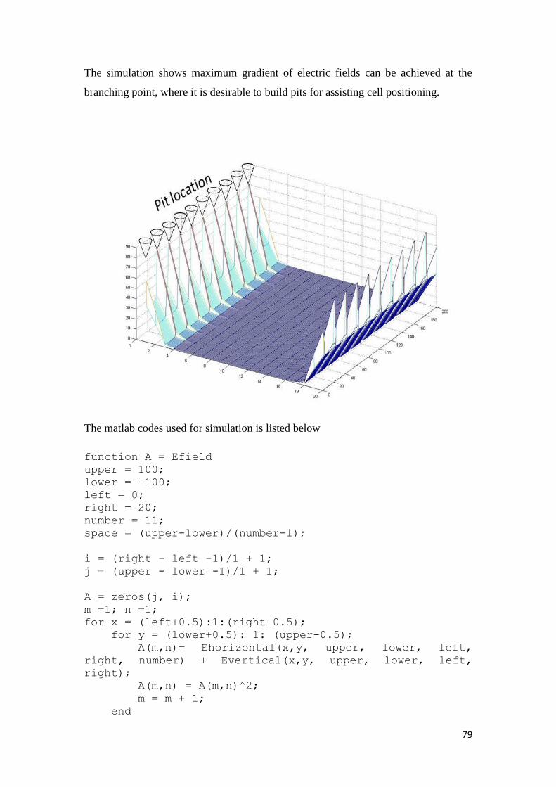
79
The simulation shows maximum gradient of electric fields can be achieved at the
branching point, where it is desirable to build pits for assisting cell positioning.
The matlab codes used for simulation is listed below
function A = Efield
upper = 100;
lower = -100;
left = 0;
right = 20;
number = 11;
space = (upper-lower)/(number-1);
i = (right - left -1)/1 + 1;
j = (upper - lower -1)/1 + 1;
A = zeros(j, i);
m =1; n =1;
for x = (left+0.5):1:(right-0.5);
for y = (lower+0.5): 1: (upper-0.5);
A(m,n)= Ehorizontal(x,y, upper, lower, left,
right, number) + Evertical(x,y, upper, lower, left,
right);
A(m,n) = A(m,n)^2;
m = m + 1;
end

80
m = 1;
n = n+1;
end
B = abs(gradient(A));
y = [(lower+0.5): 0.5 : (upper-0.5)];
x = [(left+0.5): 0.5 :(right-0.5)];
[Y X] = meshgrid(y,x);
mesh(B)
function E = Evertical(x,y, upper, lower, left, right)
E1 = 1/x*(atan((upper-y)/x)-atan((lower-y)/x));
E2 = -1/(right-x)*(atan((upper-y)/(right-x))-atan((lower-
y)/(right-x)));
E = E1+E2;
function E = Ehorizontal(x,y, upper, lower, left, right,
number)
space = (upper-lower)/(number-1);
length = (right-left)/16;
E1 = 0; E2 =0;
for i = 1:1:number;
E1 = E1+ 1/(upper-(i-1)*space-y)*(atan((length-
x)/(upper-(i-1)*space-y))-atan((-x)/(upper-(i-1)*space-
y)));
end
for i = 1:1:number;
E2 = E2- 1/(upper-(i-1)*space-y)*(atan((right-
x)/(upper-(i-1)*space-y))-atan((right-length-x)/(upper-
(i-1)*space-y)));
end
E = E1+ E2;

81
Appendix B: Data Used in Cost Modeling
It must be noted that the cost analysis here is just a rough estimation from various
literature survey; actual process may have different cost. For fixed cost, the Form 10K
from Veeco was used to assess the investment in plant, equipment as well as property.
Veeco is the leading company in the field of manufacturing AFM. Estimation from
Veeco gives an indication of the best performance one may be able to achieve with
the invested resources because among all manufacturers, Veeco has the comparative
advantage in obtaining the benefit of mass production. Veeco’s investment on plant,
equipment and property is about 16.6 million in total, which gives a production
volume of 450 AFMs a year. For the reason of simplicity, if a linear relationship
between production volume and the fixed cost is assumed, and if the production life
time is assumed to be 5 years, and all the equipment has to be upgraded after that,
there will be an average fixed cost on each machine for USD 7377.
For variable cost, the cost of manufacturing the cell chip and the AFM array was
separately calculated. The variable cost was estimated based on the processes used in
the fabrication. For the reason of estimation, the processes were divided into common
processes and unique processes, where common processes refer to the processes
which do not have distinguishing characteristics related product produced, for
example, etching, masking and MOCVD metal deposition are considered common
processes because these processes have similar costs across the production of a range
of devices. The cost of common processes can be conveniently estimated by
modeling software such as Edupack© from GRANTA Intelligence. The unique
processes refer to the processes specifically designed for the fabrication of the
proposed technological platform; these processed include piezo material spin coating.
Energy consumption is estimated based on process time and equipment power, labour
cost is estimated with hourly rate set to USD 20 per hour. The following table and
flow chart present data used in assessing the variable cost in the unique process.

82
Cr deposition as mask on Silicon wafer
13 um Cr, RIE for 7 um
KOH immersion
30 hrs CES
Thermal oxidation
zirconium-n-butoxide
dissolve Dissolve Ti{OCH(CH3)2}4
Dissolve Pb(CH3COO)2Dissolve ethylene glycol
2-propanol
1-butanol
Acetic acid
8 X Spin coating
110 5min drying
600 20 min baking
8 times
1.2 um thick layer
Anneal at 600 4 hoursAu/Cr deposition 0.2 um siO2 passivation, 0.2 um
Ar ion beam etchingKOH etching
30 Hrs Reactive ion etching
Materials Unit cost Amount cost
Zr(C4H9O4)4 USD 22/kg 0.00065 kg USD 0.014
Ti{OCH(CH3)2}4 USD 618.6/kg 0.00028 kg USD 0.175
Pb(CH3COO)2 USD 110/kg 0.00067 kg USD 0.073
ethylene glycol USD 12/L <1L USD 12
acetic acid USD 50 <1L USD 50
2-propanol USD 45 <1L USD 45
butanol USD 2 <1L USD 2
Wafer USD 80 1 USD 80
SU-8 USD 600/L 0.002L USD 1.2
Glass wafer USD 80 1 USD 80