tca6416 low-voltage 16-bit i2c and smbus i/o … · 5 4 3 2 1 p00 1 18 addr p01 2 17 p17 p02 p163...
TRANSCRIPT
ZQS PACKAGE(TOP VIEW)
E
D
C
B
A
5 4 23 1
1 18P00 ADDR
2 17P01 P17
3 16P02 P16
4 15P03 P15
5 14P04 P14
6 13P05 P13
24
7
P06
RE
SE
T
23
8
P07
VC
CI
22
9
GN
DIN
T
21
10
P10
VC
CP
20
11
P11
SD
A
19
12
P12
SC
L
RTW PACKAGE(TOP VIEW)
INT
VCCI
RESET
P00
P01
P02
P03
GND
VCCP
SDA
SCL
ADDR
P17
P16
P15
P14
1
2
3
4
5
6
7
8
12
11
10
9
PW PACKAGE(TOP VIEW)
16
15
14
13
20
19
18
17
24
23
22
21
P04
P05
P06
P07
P13
P12
P11
P10
Product
Folder
Sample &Buy
Technical
Documents
Tools &
Software
Support &Community
TCA6416SCPS153B –DECEMBER 2007–REVISED JUNE 2014
TCA6416 Low-Voltage 16-Bit I2C and SMBus I/O Expander With Interrupt Output, Reset,and Configuration Registers
Not Recommended for New Designs
1 Features • Polarity Inversion Register• Internal Power-On Reset
1• Operating Power-Supply Voltage Range of 1.65 Vto 5.5 V • Power Up With All Channels Configured as Inputs
• Allows Bidirectional Voltage-Level Translation and • No Glitch On Power UpGPIO Expansion Between: • Noise Filter on SCL/SDA Inputs– 1.8-V SCL/SDA and • Latched Outputs With High-Current Drive
1.8-V, 2.5-V, 3.3-V, or 5-V P Port Maximum Capability for Directly Driving LEDs– 2.5-V SCL/SDA and • Latch-Up Performance Exceeds 100 mA Per
1.8-V, 2.5-V, 3.3-V, or 5-V P Port JESD 78, Class II– 3.3-V SCL/SDA and • ESD Protection Exceeds JESD 22
1.8-V, 2.5-V, 3.3-V, or 5-V P Port – 2000-V Human-Body Model (A114-A)– 5-V SCL/SDA and – 200-V Machine Model (A115-A)
1.8-V, 2.5-V, 3.3-V, or 5-V P Port – 1000-V Charged-Device Model (C101)• I2C to Parallel Port Expander• Low Standby Current Consumption of 1 μA 2 Description• Schmitt-Trigger Action Allows Slow Input This 16-bit I/O expander for the two-line bidirectional
Transition and Better Switching Noise Immunity at bus (I2C) is designed to provide general-purposeremote I/O expansion for most microcontrollerthe SCL and SDA Inputsfamilies via the I2C interface [serial clock (SCL) and– Vhys = 0.18 V Typ at 1.8 Vserial data (SDA)].
– Vhys = 0.25 V Typ at 2.5 VDevice Information(1)– Vhys = 0.33 V Typ at 3.3 V
PART NUMBER PACKAGE BODY SIZE (NOM)– Vhys = 0.5 V Typ at 5 VTSSOP (24) 7.80 mm × 4.40 mm• 5-V Tolerant I/O Ports
TCA6416 WQFN (24) 4.00 mm × 4.00 mm• Active-Low Reset (RESET) InputBGA (24) 3.00 mm × 3.00 mm• Open-Drain Active-Low Interrupt (INT) Output
(1) For all available packages, see the orderable addendum at• 400-kHz Fast I2C Busthe end of the datasheet.
• Input/Output Configuration Register
1
An IMPORTANT NOTICE at the end of this data sheet addresses availability, warranty, changes, use in safety-critical applications,intellectual property matters and other important disclaimers. PRODUCTION DATA.
Not Recommended for New Designs
TCA6416SCPS153B –DECEMBER 2007–REVISED JUNE 2014 www.ti.com
Table of Contents1 Features .................................................................. 1 7 Parameter Measurement Information ................ 112 Description ............................................................. 1 8 Detailed Description ............................................ 15
8.1 Functional Block Diagram ....................................... 153 Revision History..................................................... 28.2 Device Functional Modes........................................ 174 Description (Continued) ........................................ 38.3 Programming........................................................... 195 Pin Configuration And Functions ........................ 4
9 Application And Implementation........................ 256 Specifications......................................................... 59.1 Typical Application ................................................. 256.1 Absolute Maximum Ratings ..................................... 5
10 Power Supply Recommendations ..................... 276.2 Handling Ratings ...................................................... 510.1 Power-On Reset Requirements ........................... 276.3 Recommended Operating Conditions....................... 5
11 Device and Documentation Support ................. 296.4 Electrical Characteristics........................................... 611.1 Trademarks ........................................................... 296.5 I2C Interface Timing Requirements........................... 711.2 Electrostatic Discharge Caution............................ 296.6 Reset Timing Requirements ..................................... 711.3 Glossary ................................................................ 296.7 Switching Characteristics .......................................... 7
6.8 Typical Characteristics .............................................. 8 12 Mechanical, Packaging, and OrderableInformation ........................................................... 29
3 Revision History
Changes from Revision A (February 2009) to Revision B Page
• Added RESET Errata section. .............................................................................................................................................. 17• Added Interrupt Errata section ............................................................................................................................................. 18
2 Submit Documentation Feedback Copyright © 2007–2014, Texas Instruments Incorporated
Product Folder Links: TCA6416
Not Recommended for New Designs
TCA6416www.ti.com SCPS153B –DECEMBER 2007–REVISED JUNE 2014
4 Description (Continued)The major benefit of this device is its wide VCC range. It can operate from 1.65 V to 5.5 V on the P-port side andon the SDA/SCL side. This allows the TCA6416 to interface with next-generation microprocessors andmicrocontrollers on the SDA/SCL side, where supply levels are dropping down to conserve power. In contrast tothe dropping power supplies of microprocessors and microcontrollers, some PCB components, such as LEDs,remain at a 5-V power supply.
The bidirectional voltage level translation in the TCA6416 is provided through VCCI. VCCI should be connected tothe VCC of the external SCL/SDA lines. This indicates the VCC level of the I2C bus to the TCA6416. The voltagelevel on the P-port of the TCA6416 is determined by the VCCP.
The TCA6416 consists of two 8-bit Configuration (input or output selection), Input, Output, and Polarity Inversion(active high) registers. At power on, the I/Os are configured as inputs. However, the system master can enablethe I/Os as either inputs or outputs by writing to the I/O configuration bits. The data for each input or output iskept in the corresponding input or output register. The polarity of the Input Port register can be inverted with thePolarity Inversion register. All registers can be read by the system master.
The system master can reset the TCA6416 in the event of a timeout or other improper operation by asserting alow in the RESET input. The power-on reset puts the registers in their default state and initializes the I2C/SMBusstate machine. The RESET pin causes the same reset/initialization to occur without depowering the part.
The TCA6416 open-drain interrupt (INT) output is activated when any input state differs from its correspondingInput Port register state and is used to indicate to the system master that an input state has changed.
INT can be connected to the interrupt input of a microcontroller. By sending an interrupt signal on this line, theremote I/O can inform the microcontroller if there is incoming data on its ports without having to communicate viathe I2C bus. Thus, the TCA6416 can remain a simple slave device.
The device P-port outputs have high-current sink capabilities for directly driving LEDs while consuming lowdevice current.
One hardware pin (ADDR) can be used to program and vary the fixed I2C address and allow up to two devices toshare the same I2C bus or SMBus.
Copyright © 2007–2014, Texas Instruments Incorporated Submit Documentation Feedback 3
Product Folder Links: TCA6416
ZQS PACKAGE(TOP VIEW)
E
D
C
B
A
5 4 23 1
1 18P00 ADDR
2 17P01 P17
3 16P02 P16
4 15P03 P15
5 14P04 P14
6 13P05 P13
24
7
P0
6R
ES
ET
23
8
P0
7V
CC
I
22
9
GN
DIN
T
21
10
P1
0V
CC
P
20
11
P11
SD
A
19
12
P1
2S
CL
RTW PACKAGE(TOP VIEW)
INT
VCCI
RESET
P00
P01
P02
P03
GND
VCCP
SDA
SCL
ADDR
P17
P16
P15
P14
1
2
3
4
5
6
7
8
12
11
10
9
PW PACKAGE(TOP VIEW)
16
15
14
13
20
19
18
17
24
23
22
21
P04
P05
P06
P07
P13
P12
P11
P10
Not Recommended for New Designs
TCA6416SCPS153B –DECEMBER 2007–REVISED JUNE 2014 www.ti.com
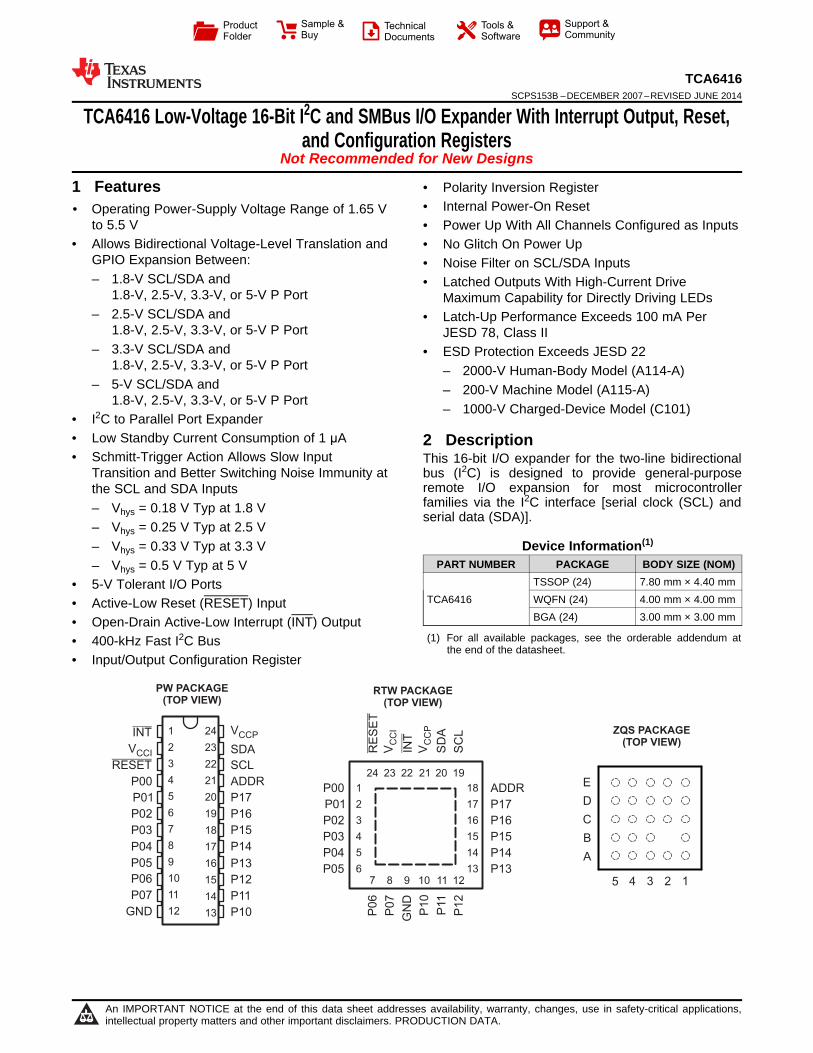
5 Pin Configuration And Functions
Pin FunctionsPIN
NO. DESCRIPTIONNAME TSSOP QFN BGA
(PW) (RTW) (ZQS)INT 1 22 A3 Interrupt output. Connect to VCCI or VCCP through a pullup resistor.
Supply voltage of I2C bus. Connect directly to the VCC of the external I2C master. ProvidesVCCI 2 23 B3 voltage-level translation.Active-low reset input. Connect to VCCP through a pullup resistor, if no active connection isRESET 3 24 A2 used.
P00 4 1 A1 P-port input/output (push-pull design structure). At power on, P00 is configured as an input.P01 5 2 C3 P-port input/output (push-pull design structure). At power on, P01 is configured as an input.P02 6 3 B1 P-port input/output (push-pull design structure). At power on, P02 is configured as an input.P03 7 4 C1 P-port input/output (push-pull design structure). At power on, P03 is configured as an input.P04 8 5 C2 P-port input/output (push-pull design structure). At power on, P04 is configured as an input.P05 9 6 D1 P-port input/output (push-pull design structure). At power on, P05 is configured as an input.P06 10 7 E1 P-port input/output (push-pull design structure). At power on, P06 is configured as an input.P07 11 8 D2 P-port input/output (push-pull design structure). At power on, P07 is configured as an input.GND 12 9 E2 GroundP10 13 10 E3 P-port input/output (push-pull design structure). At power on, P10 is configured as an input.P11 14 11 E4 P-port input/output (push-pull design structure). At power on, P11 is configured as an input.P12 15 12 D3 P-port input/output (push-pull design structure). At power on, P12 is configured as an input.P13 16 13 E5 P-port input/output (push-pull design structure). At power on, P13 is configured as an input.P14 17 14 D4 P-port input/output (push-pull design structure). At power on, P14 is configured as an input.P15 18 15 D5 P-port input/output (push-pull design structure). At power on, P15 is configured as an input.P16 19 16 C5 P-port input/output (push-pull design structure). At power on, P16 is configured as an input.P17 20 17 C4 P-port input/output (push-pull design structure). At power on, P17 is configured as an input.
ADDR 21 18 B5 Address input. Connect directly to VCCP or ground.SCL 22 19 A5 Serial clock bus. Connect to VCCI through a pullup resistor.SDA 23 20 A4 Serial data bus. Connect to VCCI through a pullup resistor.VCCP 24 21 B4 Supply voltage of TCA6416 for P port
4 Submit Documentation Feedback Copyright © 2007–2014, Texas Instruments Incorporated
Product Folder Links: TCA6416
Not Recommended for New Designs
TCA6416www.ti.com SCPS153B –DECEMBER 2007–REVISED JUNE 2014
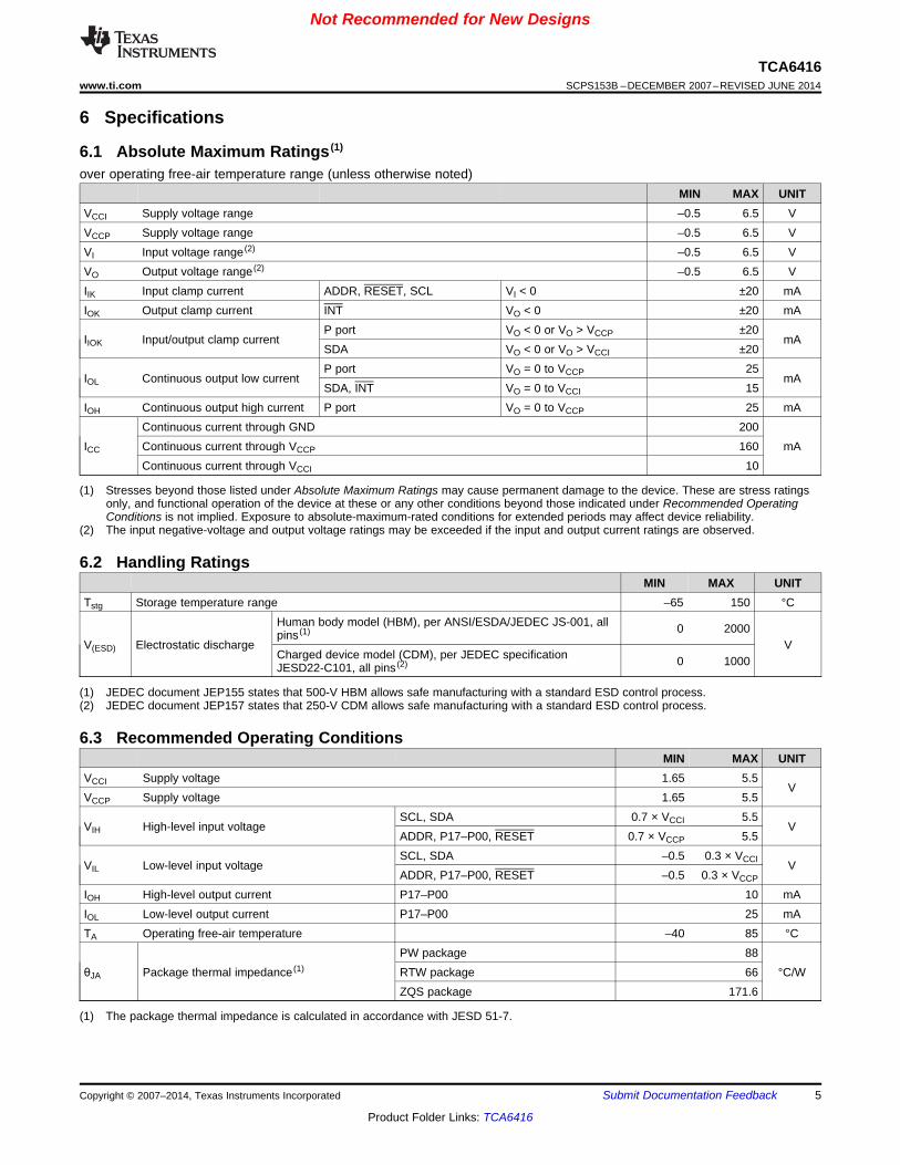
6 Specifications
6.1 Absolute Maximum Ratings (1)
over operating free-air temperature range (unless otherwise noted)MIN MAX UNIT
VCCI Supply voltage range –0.5 6.5 VVCCP Supply voltage range –0.5 6.5 VVI Input voltage range (2) –0.5 6.5 VVO Output voltage range (2) –0.5 6.5 VIIK Input clamp current ADDR, RESET, SCL VI < 0 ±20 mAIOK Output clamp current INT VO < 0 ±20 mA
P port VO < 0 or VO > VCCP ±20IIOK Input/output clamp current mA
SDA VO < 0 or VO > VCCI ±20P port VO = 0 to VCCP 25
IOL Continuous output low current mASDA, INT VO = 0 to VCCI 15
IOH Continuous output high current P port VO = 0 to VCCP 25 mAContinuous current through GND 200
ICC Continuous current through VCCP 160 mAContinuous current through VCCI 10
(1) Stresses beyond those listed under Absolute Maximum Ratings may cause permanent damage to the device. These are stress ratingsonly, and functional operation of the device at these or any other conditions beyond those indicated under Recommended OperatingConditions is not implied. Exposure to absolute-maximum-rated conditions for extended periods may affect device reliability.
(2) The input negative-voltage and output voltage ratings may be exceeded if the input and output current ratings are observed.
6.2 Handling RatingsMIN MAX UNIT
Tstg Storage temperature range –65 150 °CHuman body model (HBM), per ANSI/ESDA/JEDEC JS-001, all 0 2000pins (1)
V(ESD) Electrostatic discharge VCharged device model (CDM), per JEDEC specification 0 1000JESD22-C101, all pins (2)
(1) JEDEC document JEP155 states that 500-V HBM allows safe manufacturing with a standard ESD control process.(2) JEDEC document JEP157 states that 250-V CDM allows safe manufacturing with a standard ESD control process.
6.3 Recommended Operating ConditionsMIN MAX UNIT
VCCI Supply voltage 1.65 5.5V
VCCP Supply voltage 1.65 5.5SCL, SDA 0.7 × VCCI 5.5
VIH High-level input voltage VADDR, P17–P00, RESET 0.7 × VCCP 5.5SCL, SDA –0.5 0.3 × VCCIVIL Low-level input voltage VADDR, P17–P00, RESET –0.5 0.3 × VCCP
IOH High-level output current P17–P00 10 mAIOL Low-level output current P17–P00 25 mATA Operating free-air temperature –40 85 °C
PW package 88θJA Package thermal impedance (1) RTW package 66 °C/W
ZQS package 171.6
(1) The package thermal impedance is calculated in accordance with JESD 51-7.
Copyright © 2007–2014, Texas Instruments Incorporated Submit Documentation Feedback 5
Product Folder Links: TCA6416
Not Recommended for New Designs
TCA6416SCPS153B –DECEMBER 2007–REVISED JUNE 2014 www.ti.com
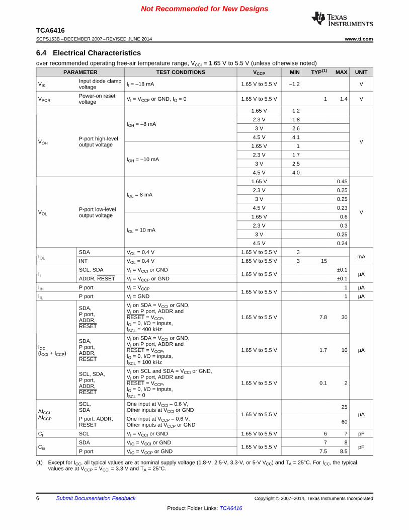
6.4 Electrical Characteristicsover recommended operating free-air temperature range, VCCI = 1.65 V to 5.5 V (unless otherwise noted)
PARAMETER TEST CONDITIONS VCCP MIN TYP (1) MAX UNITInput diode clampVIK II = –18 mA 1.65 V to 5.5 V –1.2 VvoltagePower-on resetVPOR VI = VCCP or GND, IO = 0 1.65 V to 5.5 V 1 1.4 Vvoltage
1.65 V 1.22.3 V 1.8
IOH = –8 mA3 V 2.6
4.5 V 4.1P-port high-levelVOH Voutput voltage 1.65 V 12.3 V 1.7
IOH = –10 mA3 V 2.5
4.5 V 4.01.65 V 0.452.3 V 0.25
IOL = 8 mA3 V 0.25
4.5 V 0.23P-port low-levelVOL Voutput voltage 1.65 V 0.62.3 V 0.3
IOL = 10 mA3 V 0.25
4.5 V 0.24SDA VOL = 0.4 V 1.65 V to 5.5 V 3
IOL mAINT VOL = 0.4 V 1.65 V to 5.5 V 3 15SCL, SDA VI = VCCI or GND ±0.1
II 1.65 V to 5.5 V μAADDR, RESET VI = VCCP or GND ±0.1
IIH P port VI = VCCP 1 μA1.65 V to 5.5 V
IIL P port VI = GND 1 μAVI on SDA = VCCI or GND,SDA, VI on P port, ADDR andP port, RESET = VCCP, 1.65 V to 5.5 V 7.8 30ADDR, IO = 0, I/O = inputs,RESET fSCL = 400 kHzVI on SDA = VCCI or GND,SDA, VI on P port, ADDR andICC P port, RESET = VCCP, 1.65 V to 5.5 V 1.7 10 μA(ICCI + ICCP) ADDR, IO = 0, I/O = inputs,RESET fSCL = 100 kHzVI on SCL and SDA = VCCI or GND,SCL, SDA, VI on P port, ADDR andP port, RESET = VCCP, 1.65 V to 5.5 V 0.1 2ADDR, IO = 0, I/O = inputs,RESET fSCL = 0
SCL, One input at VCCI – 0.6 V, 25SDA Other inputs at VCCI or GNDΔICCI 1.65 V to 5.5 V μAΔICCP P port, ADDR, One input at VCCP – 0.6 V, 60RESET Other inputs at VCCP or GNDCI SCL VI = VCCI or GND 1.65 V to 5.5 V 6 7 pF
SDA VIO = VCCI or GND 7 8Cio 1.65 V to 5.5 V pF
P port VIO = VCCP or GND 7.5 8.5
(1) Except for ICC, all typical values are at nominal supply voltage (1.8-V, 2.5-V, 3.3-V, or 5-V VCC) and TA = 25°C. For ICC, the typicalvalues are at VCCP = VCCI = 3.3 V and TA = 25°C.
6 Submit Documentation Feedback Copyright © 2007–2014, Texas Instruments Incorporated
Product Folder Links: TCA6416
Not Recommended for New Designs
TCA6416www.ti.com SCPS153B –DECEMBER 2007–REVISED JUNE 2014
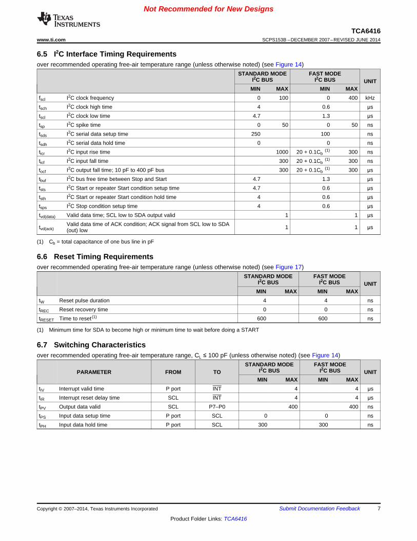
6.5 I2C Interface Timing Requirementsover recommended operating free-air temperature range (unless otherwise noted) (see Figure 14)
STANDARD MODE FAST MODEI2C BUS I2C BUS UNIT
MIN MAX MIN MAXfscl I2C clock frequency 0 100 0 400 kHztsch I2C clock high time 4 0.6 μstscl I2C clock low time 4.7 1.3 μstsp I2C spike time 0 50 0 50 nstsds I2C serial data setup time 250 100 nstsdh I2C serial data hold time 0 0 nsticr I2C input rise time 1000 20 + 0.1Cb
(1) 300 nsticf I2C input fall time 300 20 + 0.1Cb
(1) 300 nstocf I2C output fall time; 10 pF to 400 pF bus 300 20 + 0.1Cb
(1) 300 μstbuf I2C bus free time between Stop and Start 4.7 1.3 μststs I2C Start or repeater Start condition setup time 4.7 0.6 μststh I2C Start or repeater Start condition hold time 4 0.6 μstsps I2C Stop condition setup time 4 0.6 μstvd(data) Valid data time; SCL low to SDA output valid 1 1 μs
Valid data time of ACK condition; ACK signal from SCL low to SDAtvd(ack) 1 1 μs(out) low
(1) Cb = total capacitance of one bus line in pF
6.6 Reset Timing Requirementsover recommended operating free-air temperature range (unless otherwise noted) (see Figure 17)
STANDARD MODE FAST MODEI2C BUS I2C BUS UNIT
MIN MAX MIN MAXtW Reset pulse duration 4 4 nstREC Reset recovery time 0 0 nstRESET Time to reset (1) 600 600 ns
(1) Minimum time for SDA to become high or minimum time to wait before doing a START
6.7 Switching Characteristicsover recommended operating free-air temperature range, CL ≤ 100 pF (unless otherwise noted) (see Figure 14)
STANDARD MODE FAST MODEI2C BUS I2C BUSPARAMETER FROM TO UNIT
MIN MAX MIN MAXtIV Interrupt valid time P port INT 4 4 μstIR Interrupt reset delay time SCL INT 4 4 μstPV Output data valid SCL P7–P0 400 400 nstPS Input data setup time P port SCL 0 0 nstPH Input data hold time P port SCL 300 300 ns
Copyright © 2007–2014, Texas Instruments Incorporated Submit Documentation Feedback 7
Product Folder Links: TCA6416
0.50.40.30.20.1
2
4
6
8
10
12
14
16
18
20
22
24
0
0 0.6
Sin
k C
urr
en
t,m
A)
I(
SIN
K
Output Low Voltage, V)V (OL
T = 40°CA –
T = 25°CA
T = 85°CA
V = 2.5 VCC
0.50.40.30.20.1
5
10
15
20
25
30
35
40
45
50
0
0 0.6
Sin
k C
urr
en
t,m
A)
I(
SIN
K
Output Low Voltage, V)V (OL
T = 40°CA –
T = 25°CA
T = 85°CA
V = 3.3 VCC
0.60.40.30.20.1
2
4
6
8
10
12
14
16
18
20
00
V = 1.8 VCC
T = 40°CA –
0.5
Sin
k C
urr
en
t,(m
A)
I SIN
K
Output Low Voltage, V)V (OL
T = 25°CA
T = 85°CA
Su
pp
ly C
urr
en
t,I
(µA
)C
C
5.04.53.5 4.03.02.5
10
20
30
40
50
60
70
80
90
100
0
Supply Voltage, V (V)CC
2.0 5.51.65
f = 400 kHzSCL
All I/Os unloaded
8535 6010-15-40
10
20
30
40
50
60
70
80
90
100
0
f = 400 kHzSCL
All I/Os unloaded
VCC = 3.3 V
VCC = 2.5 V
V = 1.8 VCC
V = 5 VCC
Temperature, °C)T (A
Su
pp
ly C
urr
en
t,µ
A)
I(
CC
Temperature, °C)T (A
Su
pp
ly C
urr
en
t,µ
A)
I(
CC
8535 6010–15
1
2
3
4
5
6
7
8
9
0–40
SCL = VCC
All I/Os unloaded
V = 1.8 VCC
V = 2.5 VCC
V = 3.3 VCC
V = 5 VCC
Not Recommended for New Designs
TCA6416SCPS153B –DECEMBER 2007–REVISED JUNE 2014 www.ti.com
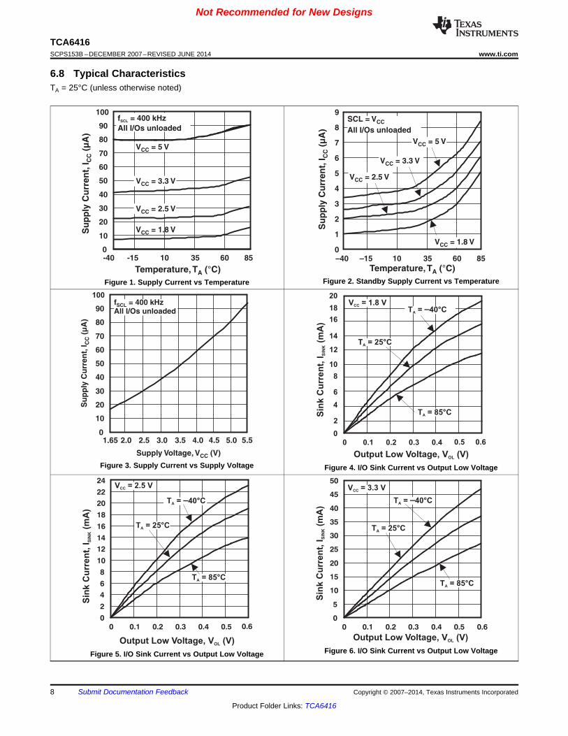
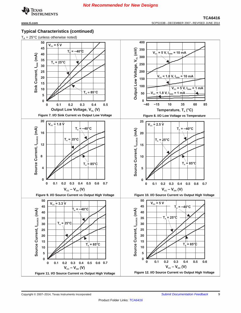
6.8 Typical CharacteristicsTA = 25°C (unless otherwise noted)
Figure 2. Standby Supply Current vs TemperatureFigure 1. Supply Current vs Temperature
Figure 3. Supply Current vs Supply Voltage Figure 4. I/O Sink Current vs Output Low Voltage
Figure 6. I/O Sink Current vs Output Low VoltageFigure 5. I/O Sink Current vs Output Low Voltage
8 Submit Documentation Feedback Copyright © 2007–2014, Texas Instruments Incorporated
Product Folder Links: TCA6416
0.60.50.3 0.40.20.1
5
10
15
20
25
30
35
40
45
50
0
0
So
urc
e C
urr
en
t,m
A)
I(
SO
UR
CE
T = 40°CA –
T = 25°CA
T = 85°CA
V = 3.3 VCC
V V (V)CC OH–
0.7 0.60.50.3 0.40.20.1
5
10
15
20
25
30
35
40
45
50
00
So
urc
e C
urr
en
t,m
A)
I(
SO
UR
CE
T = 40°CA –
T = 25°CA
T = 85°CA
V = 5 VCC
V V (V)CC OH–
0.60.50.40.30.20.1
4
8
12
16
20
0
0 0.7
So
urc
e C
urr
en
t,m
A)
I(
SO
UR
CE
T = 40°CA –
T = 25°CA
T = 85°CA
V = 1.8 VCC
V V (V)CC OH–
0.60.50.40.30.20.1
5
10
15
20
25
0
0 0.7
So
urc
e C
urr
en
t,m
A)
I(
SO
UR
CE
T = 40°CA –
T = 25°CA
T = 85°CA
V = 2.5 VCC
V V (V)CC OH–
8535 6010−15−40
50
100
150
200
250
300
350
400
0
V = 1.8 V, I = 10 mACC SINK
Ou
tpu
t L
ow
Vo
lta
ge
,m
V)
V(
OL
Temperature, °C)T (A
V = 5 V, I = 10 mACC SINK
V = 5 V, I = 1 mACC SINK
V = 1.8 V, I = 1 mACC SINK
0.40.30.20.1
5
10
15
20
25
30
35
40
45
50
00 0.5
V = 5 VCC
Sin
k C
urr
en
t,(m
A)
I SIN
K
Output Low Voltage, V (V)OL
T = 85°CA
T = 25°CA
T = 40°CA –
Not Recommended for New Designs
TCA6416www.ti.com SCPS153B –DECEMBER 2007–REVISED JUNE 2014
Typical Characteristics (continued)TA = 25°C (unless otherwise noted)
Figure 7. I/O Sink Current vs Output Low Voltage Figure 8. I/O Low Voltage vs Temperature
Figure 9. I/O Source Current vs Output High Voltage Figure 10. I/O Source Current vs Output High Voltage
Figure 12. I/O Source Current vs Output High VoltageFigure 11. I/O Source Current vs Output High Voltage
Copyright © 2007–2014, Texas Instruments Incorporated Submit Documentation Feedback 9
Product Folder Links: TCA6416
8535 6010−15−40
1
2
3
4
5
0
V = 5 V, I = 10 mACC SOURCE
V = 1.8 V, I = 10 mACC SOURCE
VV
(V)
CC
OH
–
Temperature, °C)T (A
Not Recommended for New Designs
TCA6416SCPS153B –DECEMBER 2007–REVISED JUNE 2014 www.ti.com
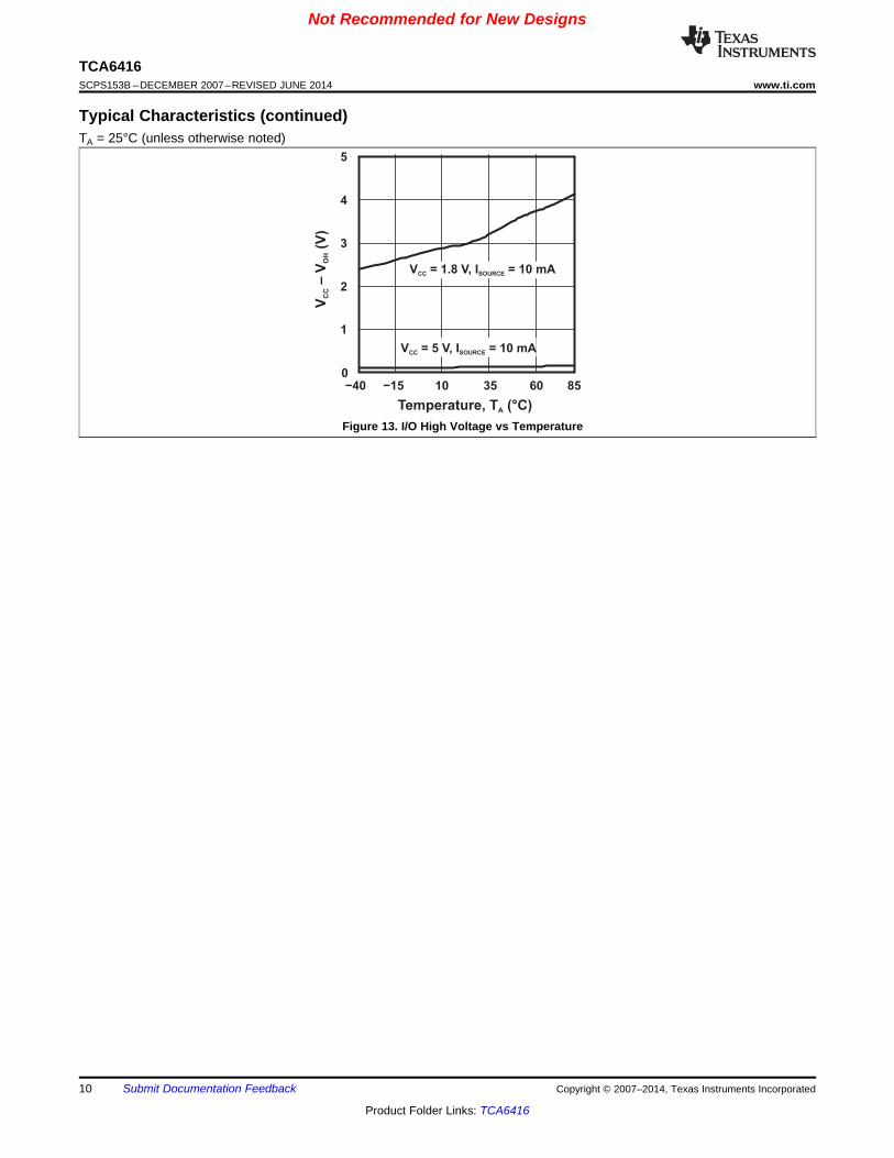
Typical Characteristics (continued)TA = 25°C (unless otherwise noted)
Figure 13. I/O High Voltage vs Temperature
10 Submit Documentation Feedback Copyright © 2007–2014, Texas Instruments Incorporated
Product Folder Links: TCA6416
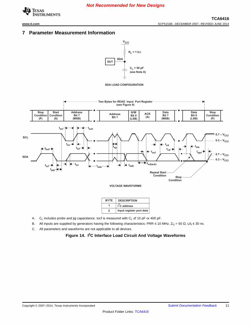
SDA LOAD CONFIGURATION
VCCI
R = 1 kL W
C = 50 pF
(see Note A)L
DUTSDA
Two Bytes for READ Input Port Register(see Figure 9)
VOLTAGE WAVEFORMS
1
2
BYTE DESCRIPTION
I C address2
Input register port data
SCL
SDA
StopCondition
(P)
StartCondition
(S)
AddressBit 7
(MSB)
AddressBit 1
R/Bit 0(LSB)
WACK(A)
DataBit 7
(MSB)
DataBit 0(LSB)
StopCondition
(P)
0.7 ´ VCCI
0.3 ´ VCCI
Repeat StartCondition
StopCondition
0.7 ´ VCCI
0.3 ´ VCCI
tscl tsch
tsp
ticf
ticf
ticr
tsth
ticr tsdstsdh
tocf
tvd(ack)
tvd
tvd
tsts
tsps
tbuf
Not Recommended for New Designs
TCA6416www.ti.com SCPS153B –DECEMBER 2007–REVISED JUNE 2014
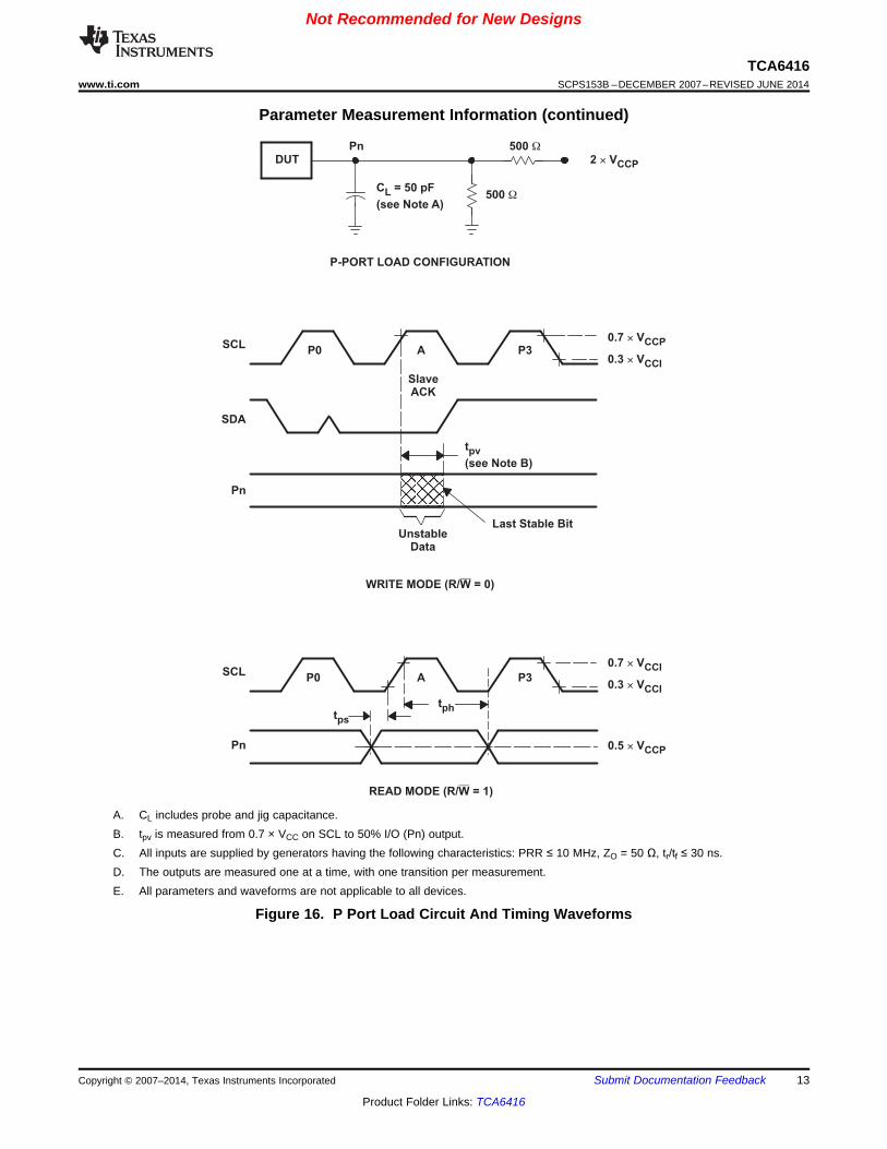
7 Parameter Measurement Information
A. CL includes probe and jig capacitance. tocf is measured with CL of 10 pF or 400 pF.B. All inputs are supplied by generators having the following characteristics: PRR ≤ 10 MHz, ZO = 50 Ω, tr/tf ≤ 30 ns.C. All parameters and waveforms are not applicable to all devices.
Figure 14. I2C Interface Load Circuit And Voltage Waveforms
Copyright © 2007–2014, Texas Instruments Incorporated Submit Documentation Feedback 11
Product Folder Links: TCA6416
A
A
A
A
S 0 1 0 0 00ADDR 1 Data 1 1 PData 2
Start
Condition 8 Bits
(One Data Byte)
From Port Data From PortSlave Address
R/W
87654321
Address Data 1 Data 2
INT
B
B
A
A
Pn INT
R/W AINT SCL
View B−BView A−A
ACK
From SlaveACK
From Slave
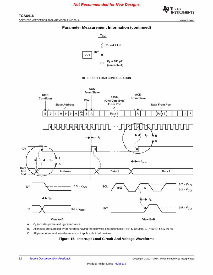
INTERRUPT LOAD CONFIGURATION
VCCI
R = 4.7 kL W
C = 100 pF
(see Note A)L
DUTINT
0.7 V´ CCI
0.3 V´ CCI
0.5 V´ CCI
0.5 V´ CCI
0.5 V´ CCP
tsps
tirtir
tiv
tiv tir
DataIntoPort
Not Recommended for New Designs
TCA6416SCPS153B –DECEMBER 2007–REVISED JUNE 2014 www.ti.com
Parameter Measurement Information (continued)
A. CL includes probe and jig capacitance.B. All inputs are supplied by generators having the following characteristics: PRR ≤ 10 MHz, ZO = 50 Ω, tr/tf ≤ 30 ns.C. All parameters and waveforms are not applicable to all devices.
Figure 15. Interrupt Load Circuit And Voltage Waveforms
12 Submit Documentation Feedback Copyright © 2007–2014, Texas Instruments Incorporated
Product Folder Links: TCA6416
P0 ASCL
P3
UnstableData
Last Stable Bit
SDA
WRITE MODE (R/ = 0)W
P0 ASCL
P3
READ MODE (R/ = 1)W
DUT
P-PORT LOAD CONFIGURATION
Pn
500 W
500 W
2 V´ CCP
0.7 V´ CCP
0.3 V´ CCI
0.7 V´ CCI
0.3 ´ VCCI
0.5 ´ VCCP
C = 50 pF
(see Note A)L
SlaveACK
t
(see Note B)pv
Pn
Pn
tps
tph
Not Recommended for New Designs
TCA6416www.ti.com SCPS153B –DECEMBER 2007–REVISED JUNE 2014
Parameter Measurement Information (continued)
A. CL includes probe and jig capacitance.B. tpv is measured from 0.7 × VCC on SCL to 50% I/O (Pn) output.C. All inputs are supplied by generators having the following characteristics: PRR ≤ 10 MHz, ZO = 50 Ω, tr/tf ≤ 30 ns.D. The outputs are measured one at a time, with one transition per measurement.E. All parameters and waveforms are not applicable to all devices.
Figure 16. P Port Load Circuit And Timing Waveforms
Copyright © 2007–2014, Texas Instruments Incorporated Submit Documentation Feedback 13
Product Folder Links: TCA6416
SDA
SCL
Start
ACK or Read Cycle
RESET
Pn
SDA LOAD CONFIGURATION
VCCI
R = 1 kWL
C = 50 pF
(see Note A)L
DUTSDA
DUT
P-PORT LOAD CONFIGURATION
Pn
500 W
500 W
2 V´ CCP
C = 50 pF
(see Note A)L
0.3 V´ CCI
V /2CCP
V /2CCP
tRESET
tRESET
tW
tREC tREC
Not Recommended for New Designs
TCA6416SCPS153B –DECEMBER 2007–REVISED JUNE 2014 www.ti.com
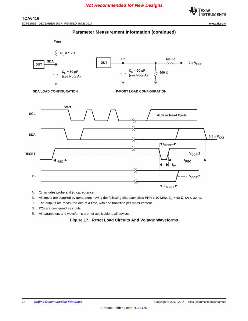
Parameter Measurement Information (continued)
A. CL includes probe and jig capacitance.B. All inputs are supplied by generators having the following characteristics: PRR ≤ 10 MHz, ZO = 50 Ω, tr/tf ≤ 30 ns.C. The outputs are measured one at a time, with one transition per measurement.D. I/Os are configured as inputs.E. All parameters and waveforms are not applicable to all devices.
Figure 17. Reset Load Circuits And Voltage Waveforms
14 Submit Documentation Feedback Copyright © 2007–2014, Texas Instruments Incorporated
Product Folder Links: TCA6416
22
I/O PortShift
Register 16 BitsInputFilter23
Power-OnReset
Read Pulse
Write Pulse
21
24
12GND
VCCP
SDA
SCL
ADDR
I C BusControl
2
RESET3
INTInterrupt
LogicLP Filter1
VCCI
2
P17–P10P07–P00
Not Recommended for New Designs
TCA6416www.ti.com SCPS153B –DECEMBER 2007–REVISED JUNE 2014
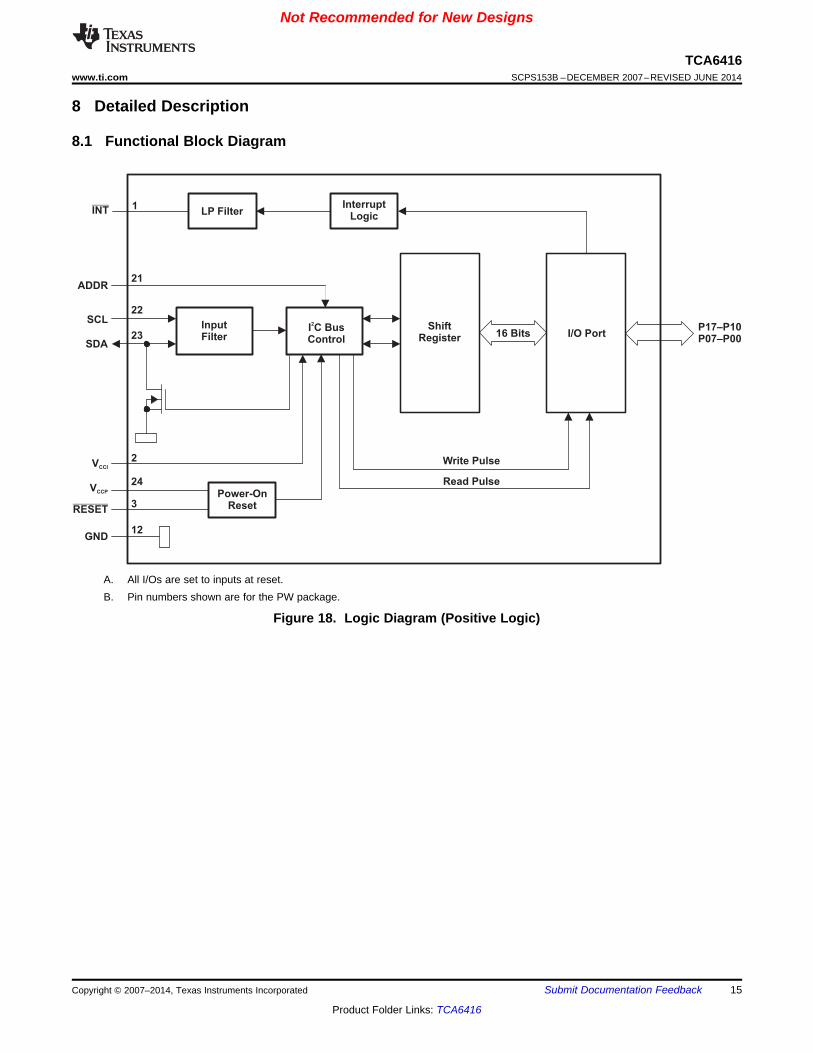
8 Detailed Description
8.1 Functional Block Diagram
A. All I/Os are set to inputs at reset.B. Pin numbers shown are for the PW package.
Figure 18. Logic Diagram (Positive Logic)
Copyright © 2007–2014, Texas Instruments Incorporated Submit Documentation Feedback 15
Product Folder Links: TCA6416
Data FromShift Register
Write ConfigurationPulse
Write Pulse
Read Pulse
Write Polarity Pulse
Polarity
Inversion
Register
Input
Port
Register
Output
Port
Register
Configuration
Register VCCP
GND
Input Port
Register Data
Polarity
Register Data
ESD Protection Diode
P00 to P17
Output Port
Register Data
To INT
Q1
Q2
D
FF
CK
Q
Q
D
FF
CK
Q
Q
D
FF
CK
Q
Q
D
FF
CK
Q
Q
Data FromShift Register
Data FromShift Register
Not Recommended for New Designs
TCA6416SCPS153B –DECEMBER 2007–REVISED JUNE 2014 www.ti.com
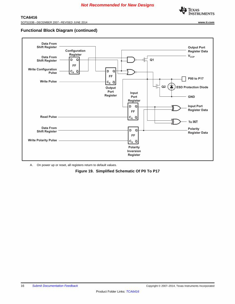
Functional Block Diagram (continued)
A. On power up or reset, all registers return to default values.
Figure 19. Simplified Schematic Of P0 To P17
16 Submit Documentation Feedback Copyright © 2007–2014, Texas Instruments Incorporated
Product Folder Links: TCA6416
Not Recommended for New Designs
TCA6416www.ti.com SCPS153B –DECEMBER 2007–REVISED JUNE 2014
8.2 Device Functional Modes
8.2.1 Voltage TranslationTable 1 shows how to set up VCC levels for the necessary voltage translation between the I2C bus and theTCA6416.
Table 1. Voltage TranslationVCCI (SDA AND SCL OF I2C VCCP (P PORT)MASTER) (V)(V)
1.8 1.81.8 2.51.8 3.31.8 52.5 1.82.5 2.52.5 3.32.5 53.3 1.83.3 2.53.3 3.33.3 55 1.85 2.55 3.35 5
8.2.2 Reset Input (RESET)The RESET input can be asserted to initialize the system while keeping the VCCP at its operating level. A resetcan be accomplished by holding the RESET pin low for a minimum of tW. The TCA6416 registers and I2C/SMBusstate machine are changed to their default state once RESET is low (0). When RESET is high (1), the I/O levelsat the P port can be changed externally or through the master. This input requires a pullup resistor to VCCP, if noactive connection is used.
8.2.2.1 RESET ErrataIf RESET voltage set higher than VCC, current will flow from RESET pin to VCC pin.
System ImpactVCC will be pulled above its regular voltage level
System WorkaroundDesign such that RESET voltage is same or lower than VCC
8.2.3 Power-On ResetWhen power (from 0 V) is applied to VCCP, an internal power-on reset holds the TCA6416 in a reset conditionuntil VCCP has reached VPOR. At that time, the reset condition is released, and the TCA6416 registers andI2C/SMBus state machine initializes to their default states. After that, VCCP must be lowered to below 0.2 V andback up to the operating voltage for a power-reset cycle.
Copyright © 2007–2014, Texas Instruments Incorporated Submit Documentation Feedback 17
Product Folder Links: TCA6416
Not Recommended for New Designs
TCA6416SCPS153B –DECEMBER 2007–REVISED JUNE 2014 www.ti.com
8.2.4 I/O PortWhen an I/O is configured as an input, FETs Q1 and Q2 (in Figure 19) are off, which creates a high-impedanceinput. The input voltage may be raised above VCC to a maximum of 5.5 V.
If the I/O is configured as an output, Q1 or Q2 is enabled, depending on the state of the output port register. Inthis case, there are low-impedance paths between the I/O pin and either VCC or GND. The external voltageapplied to this I/O pin should not exceed the recommended levels for proper operation.
8.2.5 Interrupt (INT) OutputAn interrupt is generated by any rising or falling edge of the port inputs in the input mode. After time tiv, the signalINT is valid. Resetting the interrupt circuit is achieved when data on the port is changed to the original setting,data is read from the port that generated the interrupt or in a stop event. Resetting occurs in the read mode atthe acknowledge (ACK) or not acknowledge (NACK) bit after the rising edge of the SCL signal. Interrupts thatoccur during the ACK or NACK clock pulse can be lost (or be very short) due to the resetting of the interruptduring this pulse. Each change of the I/Os after resetting is detected and is transmitted as INT.
Reading from or writing to another device does not affect the interrupt circuit, and a pin configured as an outputcannot cause an interrupt. Changing an I/O from an output to an input may cause a false interrupt to occur, if thestate of the pin does not match the contents of the Input Port register.
In the TCA6416, an interrupt is not immediately generated by any rising or falling edge of port inputs in inputmode after issuing any I2C commands (read or write). In order to capture the INT in the TCA6416, the userneeds to add one more SCL clock pulse after a Stop signal.
The INT output has an open-drain structure and requires a pullup resistor to VCCP or VCCI depending on theapplication. If the INT signal is connected back to the processor that provides the SCL signal to the TCA6416,then the INT pin has to be connected to VCCI. If not, the INT pin can be connected to VCCP.
8.2.5.1 Interrupt ErrataThe INT will be improperly de-asserted if the following two conditions occur:1. The last I2C command byte (register pointer) written to the device was 00h.
NOTEThis generally means the last operation with the device was a Read of the input register.However, the command byte may have been written with 00h without ever going on toread the input register. After reading from the device, if no other command byte written, itwill remain 00h.
2. Any other slave device on the I2C bus acknowledges an address byte with the R/W bit set high
System ImpactCan cause improper interrupt handling as the Master will see the interrupt as being cleared.
System WorkaroundMinor software change: User must change command byte to something besides 00h after a Read operation tothe TCA6416 device or before reading from another slave device.
NOTESoftware change will be compatible with other versions (competition and TI redesigns) ofthis device.
18 Submit Documentation Feedback Copyright © 2007–2014, Texas Instruments Incorporated
Product Folder Links: TCA6416
SDA
SCL
Data Line Change
SDA
SCLS P
Start Condition Stop Condition
Not Recommended for New Designs
TCA6416www.ti.com SCPS153B –DECEMBER 2007–REVISED JUNE 2014
8.3 Programming
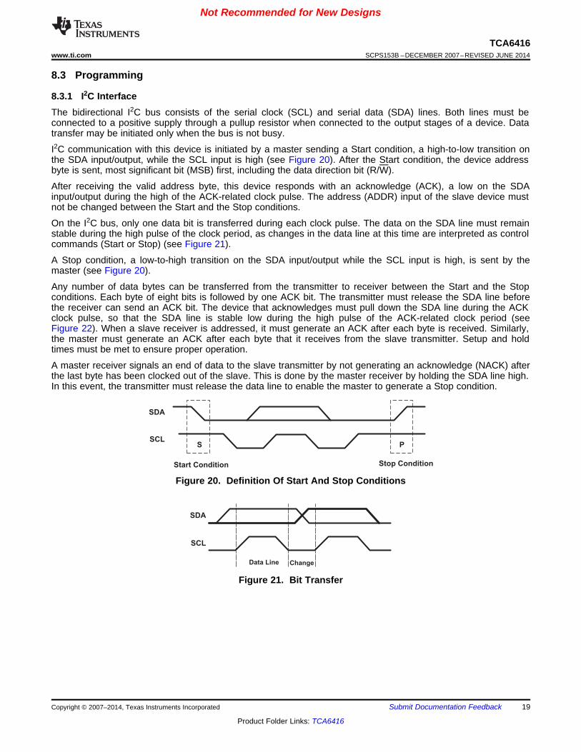
8.3.1 I2C InterfaceThe bidirectional I2C bus consists of the serial clock (SCL) and serial data (SDA) lines. Both lines must beconnected to a positive supply through a pullup resistor when connected to the output stages of a device. Datatransfer may be initiated only when the bus is not busy.
I2C communication with this device is initiated by a master sending a Start condition, a high-to-low transition onthe SDA input/output, while the SCL input is high (see Figure 20). After the Start condition, the device addressbyte is sent, most significant bit (MSB) first, including the data direction bit (R/W).
After receiving the valid address byte, this device responds with an acknowledge (ACK), a low on the SDAinput/output during the high of the ACK-related clock pulse. The address (ADDR) input of the slave device mustnot be changed between the Start and the Stop conditions.
On the I2C bus, only one data bit is transferred during each clock pulse. The data on the SDA line must remainstable during the high pulse of the clock period, as changes in the data line at this time are interpreted as controlcommands (Start or Stop) (see Figure 21).
A Stop condition, a low-to-high transition on the SDA input/output while the SCL input is high, is sent by themaster (see Figure 20).
Any number of data bytes can be transferred from the transmitter to receiver between the Start and the Stopconditions. Each byte of eight bits is followed by one ACK bit. The transmitter must release the SDA line beforethe receiver can send an ACK bit. The device that acknowledges must pull down the SDA line during the ACKclock pulse, so that the SDA line is stable low during the high pulse of the ACK-related clock period (seeFigure 22). When a slave receiver is addressed, it must generate an ACK after each byte is received. Similarly,the master must generate an ACK after each byte that it receives from the slave transmitter. Setup and holdtimes must be met to ensure proper operation.
A master receiver signals an end of data to the slave transmitter by not generating an acknowledge (NACK) afterthe last byte has been clocked out of the slave. This is done by the master receiver by holding the SDA line high.In this event, the transmitter must release the data line to enable the master to generate a Stop condition.
Figure 20. Definition Of Start And Stop Conditions
Figure 21. Bit Transfer
Copyright © 2007–2014, Texas Instruments Incorporated Submit Documentation Feedback 19
Product Folder Links: TCA6416
0
Slave Address
1 0 0 0 0 ADDR R/W
FixedProgrammable
S
1 2 8 9
NACK
ACK
Data Outputby Transmitter
Data Outputby Receiver
SCL FromMaster
StartCondition
Clock Pulse forAcknowledgment
Not Recommended for New Designs
TCA6416SCPS153B –DECEMBER 2007–REVISED JUNE 2014 www.ti.com
Programming (continued)
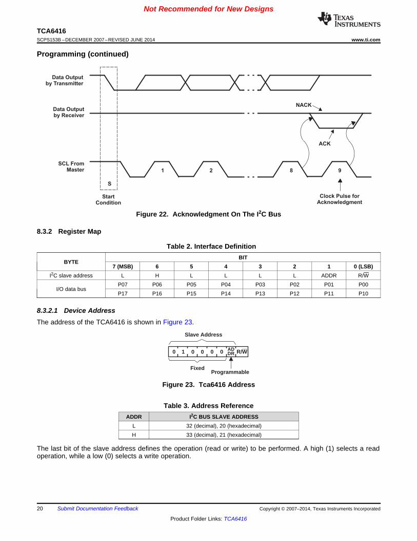
Figure 22. Acknowledgment On The I2C Bus
8.3.2 Register Map
Table 2. Interface DefinitionBIT
BYTE7 (MSB) 6 5 4 3 2 1 0 (LSB)
I2C slave address L H L L L L ADDR R/WP07 P06 P05 P04 P03 P02 P01 P00
I/O data busP17 P16 P15 P14 P13 P12 P11 P10
8.3.2.1 Device AddressThe address of the TCA6416 is shown in Figure 23.
Figure 23. Tca6416 Address
Table 3. Address ReferenceADDR I2C BUS SLAVE ADDRESS
L 32 (decimal), 20 (hexadecimal)H 33 (decimal), 21 (hexadecimal)
The last bit of the slave address defines the operation (read or write) to be performed. A high (1) selects a readoperation, while a low (0) selects a write operation.
20 Submit Documentation Feedback Copyright © 2007–2014, Texas Instruments Incorporated
Product Folder Links: TCA6416
B2 B1 B0B5 B4 B3B7 B6
Not Recommended for New Designs
TCA6416www.ti.com SCPS153B –DECEMBER 2007–REVISED JUNE 2014
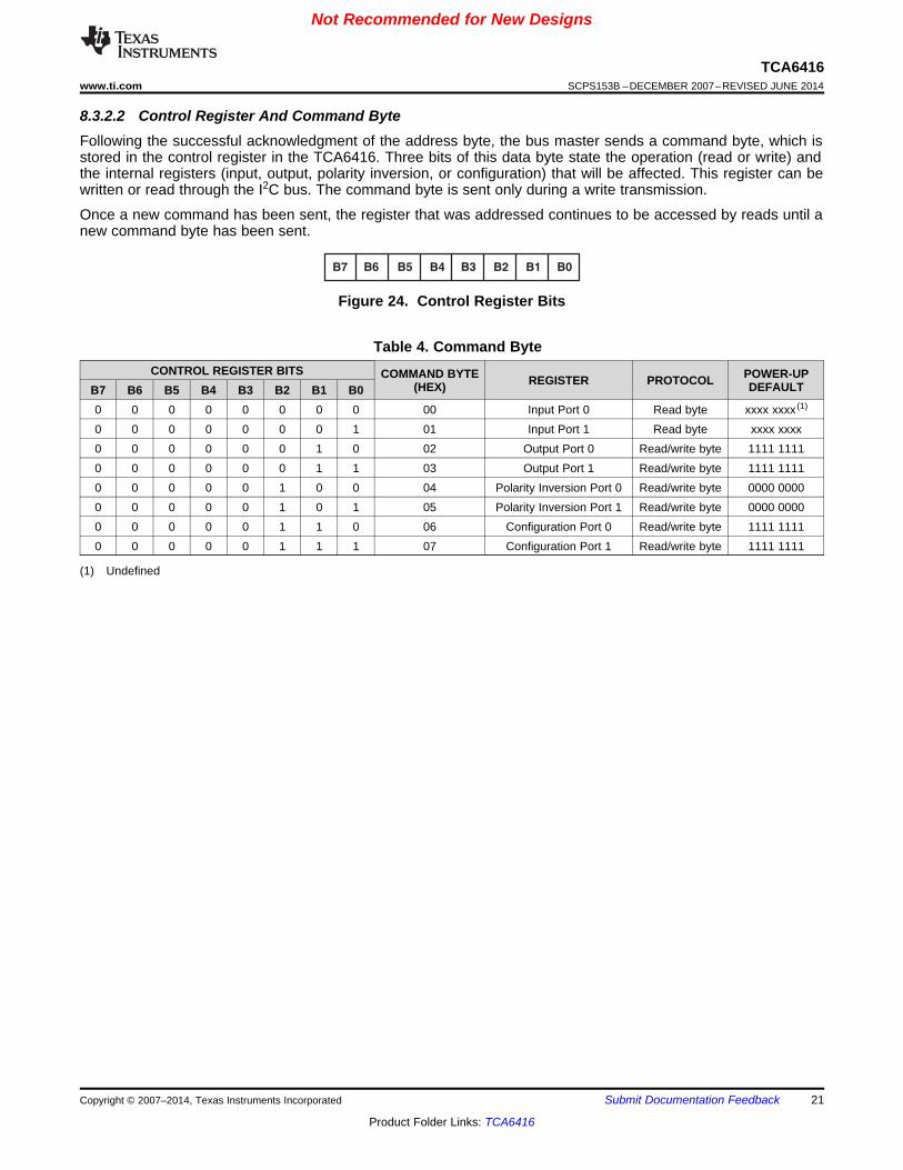
8.3.2.2 Control Register And Command ByteFollowing the successful acknowledgment of the address byte, the bus master sends a command byte, which isstored in the control register in the TCA6416. Three bits of this data byte state the operation (read or write) andthe internal registers (input, output, polarity inversion, or configuration) that will be affected. This register can bewritten or read through the I2C bus. The command byte is sent only during a write transmission.
Once a new command has been sent, the register that was addressed continues to be accessed by reads until anew command byte has been sent.
Figure 24. Control Register Bits
Table 4. Command ByteCONTROL REGISTER BITS COMMAND BYTE POWER-UPREGISTER PROTOCOL(HEX) DEFAULTB7 B6 B5 B4 B3 B2 B1 B0
0 0 0 0 0 0 0 0 00 Input Port 0 Read byte xxxx xxxx (1)
0 0 0 0 0 0 0 1 01 Input Port 1 Read byte xxxx xxxx0 0 0 0 0 0 1 0 02 Output Port 0 Read/write byte 1111 11110 0 0 0 0 0 1 1 03 Output Port 1 Read/write byte 1111 11110 0 0 0 0 1 0 0 04 Polarity Inversion Port 0 Read/write byte 0000 00000 0 0 0 0 1 0 1 05 Polarity Inversion Port 1 Read/write byte 0000 00000 0 0 0 0 1 1 0 06 Configuration Port 0 Read/write byte 1111 11110 0 0 0 0 1 1 1 07 Configuration Port 1 Read/write byte 1111 1111
(1) Undefined
Copyright © 2007–2014, Texas Instruments Incorporated Submit Documentation Feedback 21
Product Folder Links: TCA6416
Not Recommended for New Designs
TCA6416SCPS153B –DECEMBER 2007–REVISED JUNE 2014 www.ti.com
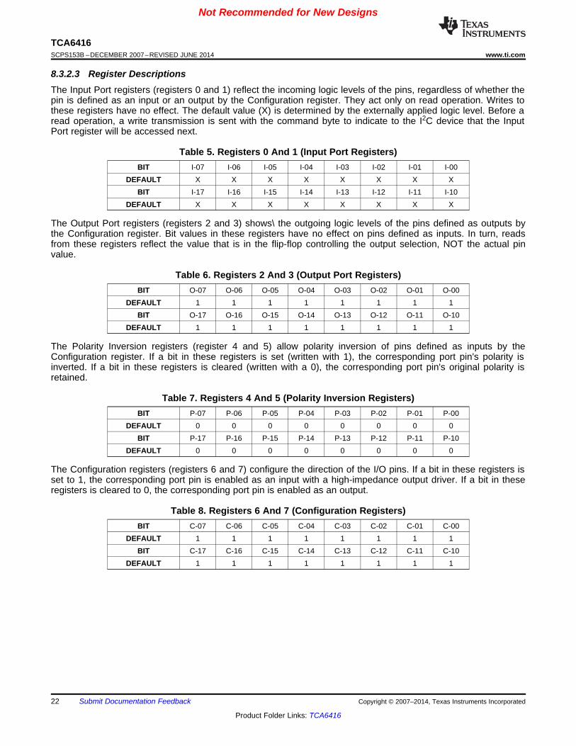
8.3.2.3 Register DescriptionsThe Input Port registers (registers 0 and 1) reflect the incoming logic levels of the pins, regardless of whether thepin is defined as an input or an output by the Configuration register. They act only on read operation. Writes tothese registers have no effect. The default value (X) is determined by the externally applied logic level. Before aread operation, a write transmission is sent with the command byte to indicate to the I2C device that the InputPort register will be accessed next.
Table 5. Registers 0 And 1 (Input Port Registers)BIT I-07 I-06 I-05 I-04 I-03 I-02 I-01 I-00
DEFAULT X X X X X X X XBIT I-17 I-16 I-15 I-14 I-13 I-12 I-11 I-10
DEFAULT X X X X X X X X
The Output Port registers (registers 2 and 3) shows\ the outgoing logic levels of the pins defined as outputs bythe Configuration register. Bit values in these registers have no effect on pins defined as inputs. In turn, readsfrom these registers reflect the value that is in the flip-flop controlling the output selection, NOT the actual pinvalue.
Table 6. Registers 2 And 3 (Output Port Registers)BIT O-07 O-06 O-05 O-04 O-03 O-02 O-01 O-00
DEFAULT 1 1 1 1 1 1 1 1BIT O-17 O-16 O-15 O-14 O-13 O-12 O-11 O-10
DEFAULT 1 1 1 1 1 1 1 1
The Polarity Inversion registers (register 4 and 5) allow polarity inversion of pins defined as inputs by theConfiguration register. If a bit in these registers is set (written with 1), the corresponding port pin's polarity isinverted. If a bit in these registers is cleared (written with a 0), the corresponding port pin's original polarity isretained.
Table 7. Registers 4 And 5 (Polarity Inversion Registers)BIT P-07 P-06 P-05 P-04 P-03 P-02 P-01 P-00
DEFAULT 0 0 0 0 0 0 0 0BIT P-17 P-16 P-15 P-14 P-13 P-12 P-11 P-10
DEFAULT 0 0 0 0 0 0 0 0
The Configuration registers (registers 6 and 7) configure the direction of the I/O pins. If a bit in these registers isset to 1, the corresponding port pin is enabled as an input with a high-impedance output driver. If a bit in theseregisters is cleared to 0, the corresponding port pin is enabled as an output.
Table 8. Registers 6 And 7 (Configuration Registers)BIT C-07 C-06 C-05 C-04 C-03 C-02 C-01 C-00
DEFAULT 1 1 1 1 1 1 1 1BIT C-17 C-16 C-15 C-14 C-13 C-12 C-11 C-10
DEFAULT 1 1 1 1 1 1 1 1
22 Submit Documentation Feedback Copyright © 2007–2014, Texas Instruments Incorporated
Product Folder Links: TCA6416
1 2SCL 3 4 5 6 7 8
SDA A A AData 0
Data t Registero
R/W
9
0/10 0 0 0 0 1 1/0 MSB LSB Data1MSB LSB AS 0 1 0 0 0 0 ADDR 0
1 2 3 4 5 6 7 8 9 1 2 3 4 5 6 7 8 9 1 2 3 4 5
P
AcknowledgeFrom Slave
AcknowledgeFrom Slave
Start Condition
Command ByteSlave Address
AcknowledgeFrom Slave
Data t Registero
1 2SCL 3 4 5 6 7 8
SDA A A AData 0
R/W
tpv
9
00 0 0 0 0 0 1 0.7 0.0 Data 11.7 1.0 AS 0 1 0 0 0 0 ADDR 0 P
Slave Address Command Byte Data to Port 0 Data to Port 1
Start Condition AcknowledgeFrom Slave
Write to Port
Data Out from Port 1
Data Out from Port 0
Data Valid
AcknowledgeFrom Slave
AcknowledgeFrom Slave
tpv
Not Recommended for New Designs
TCA6416www.ti.com SCPS153B –DECEMBER 2007–REVISED JUNE 2014
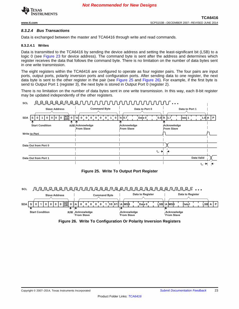
8.3.2.4 Bus TransactionsData is exchanged between the master and TCA6416 through write and read commands.
8.3.2.4.1 Writes
Data is transmitted to the TCA6416 by sending the device address and setting the least-significant bit (LSB) to alogic 0 (see Figure 23 for device address). The command byte is sent after the address and determines whichregister receives the data that follows the command byte. There is no limitation on the number of data bytes sentin one write transmission.
The eight registers within the TCA6416 are configured to operate as four register pairs. The four pairs are inputports, output ports, polarity inversion ports and configuration ports. After sending data to one register, the nextdata byte is sent to the other register in the pair (see Figure 25 and Figure 26). For example, if the first byte issend to Output Port 1 (register 3), the next byte is stored in Output Port 0 (register 2).
There is no limitation on the number of data bytes sent in one write transmission. In this way, each 8-bit registermay be updated independently of the other registers.
Figure 25. Write To Output Port Register
<br/>
Figure 26. Write To Configuration Or Polarity Inversion Registers
Copyright © 2007–2014, Texas Instruments Incorporated Submit Documentation Feedback 23
Product Folder Links: TCA6416
1 2 3 4 5 6 7 8 9
S 0 1 0 0 0 0ADDR 1 1A 1 A
I0.x
A
I1.x
A
I0.x I1.x
P
SCL
SDA
INT
Read FromPort 0
Data IntoPort 0
Read FromPort 1
Data IntoPort 1
AcknowledgeFrom Master
AcknowledgeFrom Slave
AcknowledgeFrom Master
AcknowledgeFrom Master
No AcknowledgeFrom Master
tiv tir
R/W
Data 1 Data 2 Data 3 Data 4
0 0 0 0 ADDR0 1S 0 A A A
R/W
A
PNA
S 1 MSB LSB
MSB LSB
Slave AddressAcknowledgeFrom Slave
Command Byte
Data From Upperor Lower Byte
of Register
Last Byte
Data
AcknowledgeFrom Slave
AcknowledgeFrom SlaveSlave Address
Data From Loweror Upper Byte
of Register
First Byte
Data
No AcknowledgeFrom Master
AcknowledgeFrom Master
At this moment, master transmitter
slave transmitter.becomes master receiver, and
slave receiver becomes
0 0 0 0 ADDR0 1
R/W
Not Recommended for New Designs
TCA6416SCPS153B –DECEMBER 2007–REVISED JUNE 2014 www.ti.com
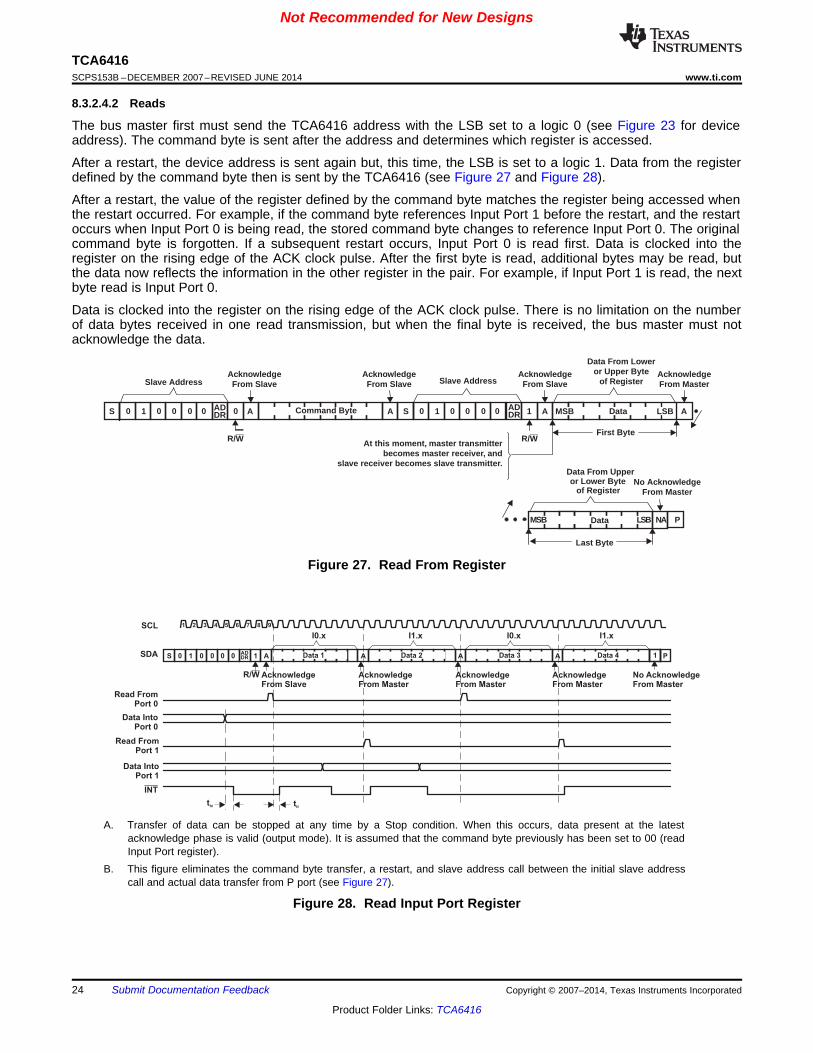
8.3.2.4.2 Reads
The bus master first must send the TCA6416 address with the LSB set to a logic 0 (see Figure 23 for deviceaddress). The command byte is sent after the address and determines which register is accessed.
After a restart, the device address is sent again but, this time, the LSB is set to a logic 1. Data from the registerdefined by the command byte then is sent by the TCA6416 (see Figure 27 and Figure 28).
After a restart, the value of the register defined by the command byte matches the register being accessed whenthe restart occurred. For example, if the command byte references Input Port 1 before the restart, and the restartoccurs when Input Port 0 is being read, the stored command byte changes to reference Input Port 0. The originalcommand byte is forgotten. If a subsequent restart occurs, Input Port 0 is read first. Data is clocked into theregister on the rising edge of the ACK clock pulse. After the first byte is read, additional bytes may be read, butthe data now reflects the information in the other register in the pair. For example, if Input Port 1 is read, the nextbyte read is Input Port 0.
Data is clocked into the register on the rising edge of the ACK clock pulse. There is no limitation on the numberof data bytes received in one read transmission, but when the final byte is received, the bus master must notacknowledge the data.
Figure 27. Read From Register
<br/>
A. Transfer of data can be stopped at any time by a Stop condition. When this occurs, data present at the latestacknowledge phase is valid (output mode). It is assumed that the command byte previously has been set to 00 (readInput Port register).
B. This figure eliminates the command byte transfer, a restart, and slave address call between the initial slave addresscall and actual data transfer from P port (see Figure 27).
Figure 28. Read Input Port Register
24 Submit Documentation Feedback Copyright © 2007–2014, Texas Instruments Incorporated
Product Folder Links: TCA6416
P00
ADDR
P12
P13
P14
P15
GND
INT
SDA
SCL
TCA6416
SDA
SCL
INT
GND
Master
Controller
P02
P01
P03
P04
P05
P06
P07
P10
P11
P16
P17
22
2
23
1
21
12
24
RESET3
RESET
V
(1.8 V)CCI
VCC
VCCP
10 kW 10 kW 10 kW
10 kW
VCCPVCCI
VCCI
Keypad
ALARM
Subsystem 1
(e.g., Alarm)
A
B
4
ENABLE
5
10 k (x 7)W
6
7
8
9
10
11
13
14
15
16
17
18
19
20
(See Note E)
Not Recommended for New Designs
TCA6416www.ti.com SCPS153B –DECEMBER 2007–REVISED JUNE 2014
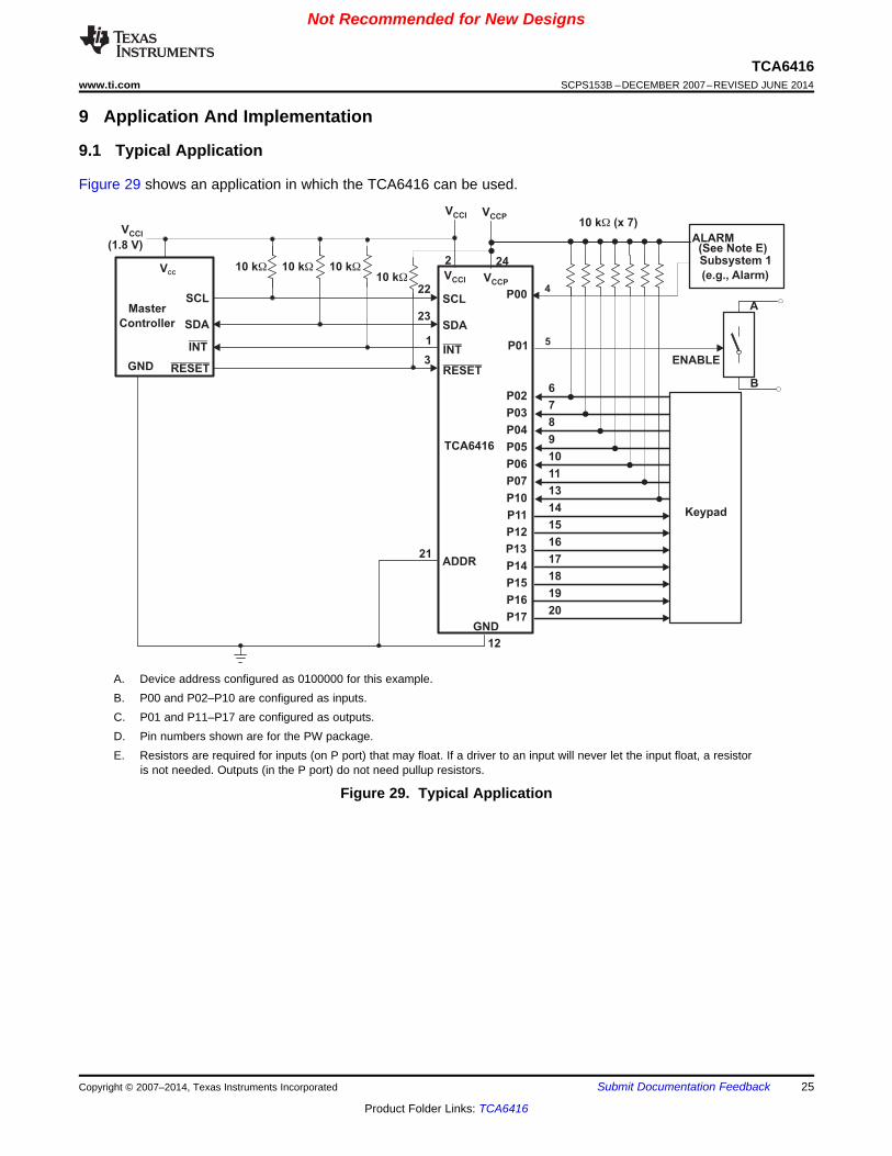
9 Application And Implementation
9.1 Typical Application
Figure 29 shows an application in which the TCA6416 can be used.
A. Device address configured as 0100000 for this example.B. P00 and P02–P10 are configured as inputs.C. P01 and P11–P17 are configured as outputs.D. Pin numbers shown are for the PW package.E. Resistors are required for inputs (on P port) that may float. If a driver to an input will never let the input float, a resistor
is not needed. Outputs (in the P port) do not need pullup resistors.
Figure 29. Typical Application
Copyright © 2007–2014, Texas Instruments Incorporated Submit Documentation Feedback 25
Product Folder Links: TCA6416
3.3 V
Px
LED
5 V
VCC
Px
LED
100 kWV
CC
VCC
Not Recommended for New Designs
TCA6416SCPS153B –DECEMBER 2007–REVISED JUNE 2014 www.ti.com
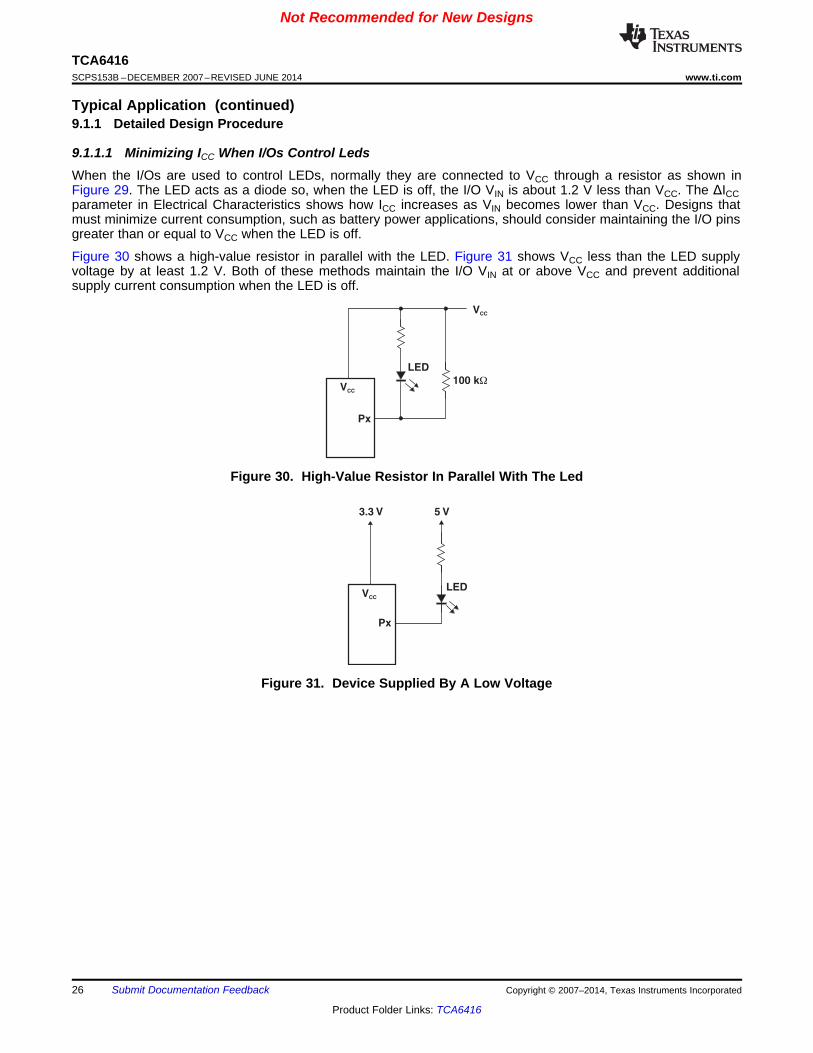
Typical Application (continued)9.1.1 Detailed Design Procedure
9.1.1.1 Minimizing ICC When I/Os Control LedsWhen the I/Os are used to control LEDs, normally they are connected to VCC through a resistor as shown inFigure 29. The LED acts as a diode so, when the LED is off, the I/O VIN is about 1.2 V less than VCC. The ΔICCparameter in Electrical Characteristics shows how ICC increases as VIN becomes lower than VCC. Designs thatmust minimize current consumption, such as battery power applications, should consider maintaining the I/O pinsgreater than or equal to VCC when the LED is off.
Figure 30 shows a high-value resistor in parallel with the LED. Figure 31 shows VCC less than the LED supplyvoltage by at least 1.2 V. Both of these methods maintain the I/O VIN at or above VCC and prevent additionalsupply current consumption when the LED is off.
Figure 30. High-Value Resistor In Parallel With The Led
Figure 31. Device Supplied By A Low Voltage
26 Submit Documentation Feedback Copyright © 2007–2014, Texas Instruments Incorporated
Product Folder Links: TCA6416
VCC
Ramp-Up
Time to Re-Ramp
Time
Ramp-Down
VIN drops below POR levels
VCC_RTVCC_FT
VCC_TRR_VPOR50
VCC
Ramp-Up Re-Ramp-Up
Time to Re-Ramp
Time
Ramp-Down
VCC_RT VCC_RTVCC_FT
VCC_TRR_GND
Not Recommended for New Designs
TCA6416www.ti.com SCPS153B –DECEMBER 2007–REVISED JUNE 2014
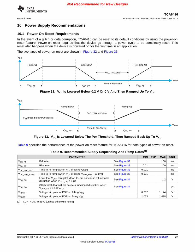
10 Power Supply Recommendations
10.1 Power-On Reset RequirementsIn the event of a glitch or data corruption, TCA6416 can be reset to its default conditions by using the power-onreset feature. Power-on reset requires that the device go through a power cycle to be completely reset. Thisreset also happens when the device is powered on for the first time in an application.
The two types of power-on reset are shown in Figure 32 and Figure 33.
Figure 32. VCC Is Lowered Below 0.2 V Or 0 V And Then Ramped Up To VCC
Figure 33. VCC Is Lowered Below The Por Threshold, Then Ramped Back Up To VCC
Table 9 specifies the performance of the power-on reset feature for TCA6416 for both types of power-on reset.
Table 9. Recommended Supply Sequencing And Ramp Rates (1)
PARAMETER MIN TYP MAX UNITVCC_FT Fall rate See Figure 32 1 100 msVCC_RT Rise rate See Figure 32 0.01 100 msVCC_TRR_GND Time to re-ramp (when VCC drops to GND) See Figure 32 0.001 msVCC_TRR_POR50 Time to re-ramp (when VCC drops to VPOR_MIN – 50 mV) See Figure 33 0.001 ms
Level that VCCP can glitch down to, but not cause a functionalVCC_GH See Figure 34 1.2 Vdisruption when VCCX_GW = 1 μsGlitch width that will not cause a functional disruption whenVCC_GW See Figure 34 μsVCCX_GH = 0.5 × VCCx
VPORF Voltage trip point of POR on falling VCC 0.767 1.144 VVPORR Voltage trip point of POR on fising VCC 1.033 1.428 V
(1) TA = –40°C to 85°C (unless otherwise noted)
Copyright © 2007–2014, Texas Instruments Incorporated Submit Documentation Feedback 27
Product Folder Links: TCA6416
VCC
VPOR
VPORF
Time
POR
Time
VCC
Time
VCC_GH
VCC_GW
Not Recommended for New Designs
TCA6416SCPS153B –DECEMBER 2007–REVISED JUNE 2014 www.ti.com
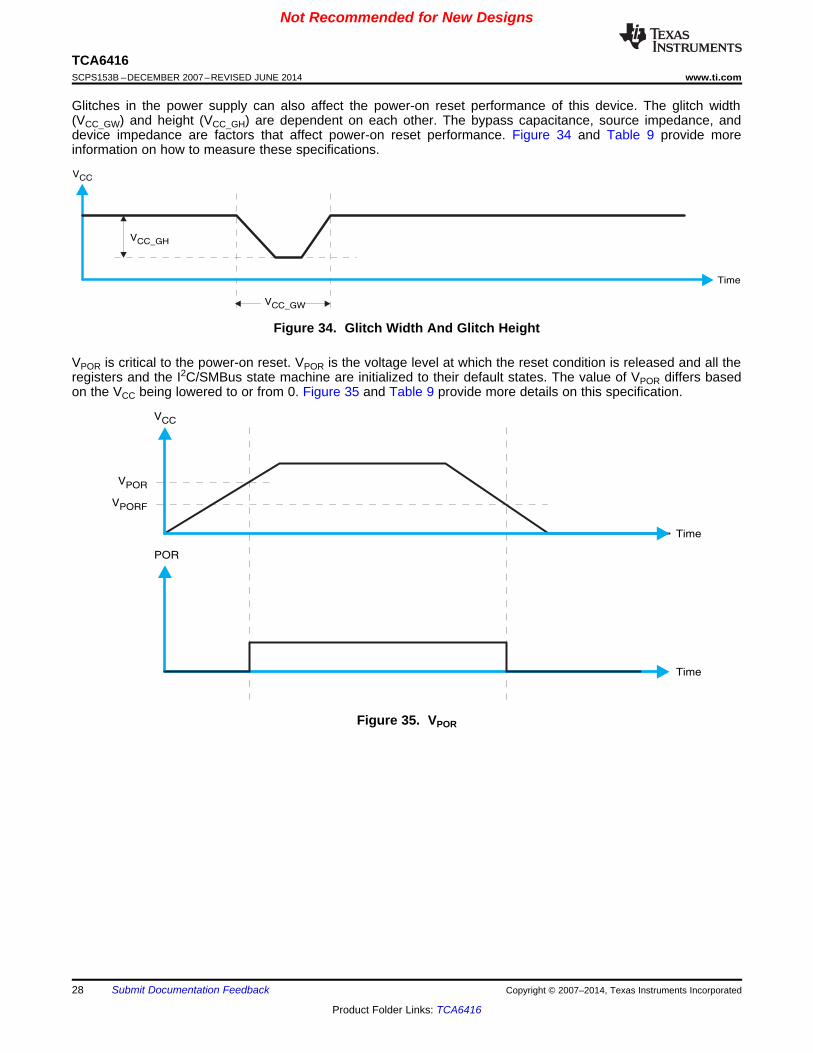
Glitches in the power supply can also affect the power-on reset performance of this device. The glitch width(VCC_GW) and height (VCC_GH) are dependent on each other. The bypass capacitance, source impedance, anddevice impedance are factors that affect power-on reset performance. Figure 34 and Table 9 provide moreinformation on how to measure these specifications.
Figure 34. Glitch Width And Glitch Height
VPOR is critical to the power-on reset. VPOR is the voltage level at which the reset condition is released and all theregisters and the I2C/SMBus state machine are initialized to their default states. The value of VPOR differs basedon the VCC being lowered to or from 0. Figure 35 and Table 9 provide more details on this specification.
Figure 35. VPOR
28 Submit Documentation Feedback Copyright © 2007–2014, Texas Instruments Incorporated
Product Folder Links: TCA6416
Not Recommended for New Designs
TCA6416www.ti.com SCPS153B –DECEMBER 2007–REVISED JUNE 2014
11 Device and Documentation Support
11.1 TrademarksAll trademarks are the property of their respective owners.
11.2 Electrostatic Discharge CautionThese devices have limited built-in ESD protection. The leads should be shorted together or the device placed in conductive foamduring storage or handling to prevent electrostatic damage to the MOS gates.
11.3 GlossarySLYZ022 — TI Glossary.
This glossary lists and explains terms, acronyms, and definitions.
12 Mechanical, Packaging, and Orderable InformationThe following pages include mechanical, packaging, and orderable information. This information is the mostcurrent data available for the designated devices. This data is subject to change without notice and revision ofthis document. For browser-based versions of this data sheet, refer to the left-hand navigation.
Copyright © 2007–2014, Texas Instruments Incorporated Submit Documentation Feedback 29
Product Folder Links: TCA6416
PACKAGE OPTION ADDENDUM
www.ti.com 10-Jun-2014
Addendum-Page 1
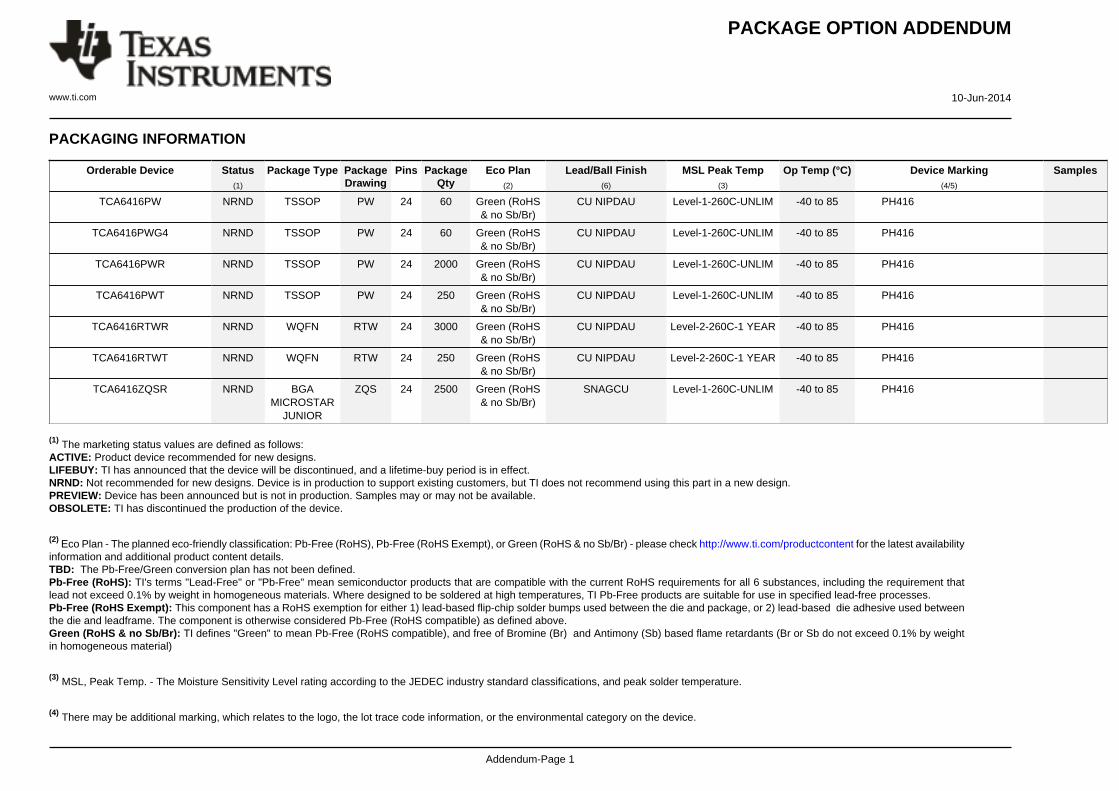
PACKAGING INFORMATION
Orderable Device Status(1)
Package Type PackageDrawing
Pins PackageQty
Eco Plan(2)
Lead/Ball Finish(6)
MSL Peak Temp(3)
Op Temp (°C) Device Marking(4/5)
Samples
TCA6416PW NRND TSSOP PW 24 60 Green (RoHS& no Sb/Br)
CU NIPDAU Level-1-260C-UNLIM -40 to 85 PH416
TCA6416PWG4 NRND TSSOP PW 24 60 Green (RoHS& no Sb/Br)
CU NIPDAU Level-1-260C-UNLIM -40 to 85 PH416
TCA6416PWR NRND TSSOP PW 24 2000 Green (RoHS& no Sb/Br)
CU NIPDAU Level-1-260C-UNLIM -40 to 85 PH416
TCA6416PWT NRND TSSOP PW 24 250 Green (RoHS& no Sb/Br)
CU NIPDAU Level-1-260C-UNLIM -40 to 85 PH416
TCA6416RTWR NRND WQFN RTW 24 3000 Green (RoHS& no Sb/Br)
CU NIPDAU Level-2-260C-1 YEAR -40 to 85 PH416
TCA6416RTWT NRND WQFN RTW 24 250 Green (RoHS& no Sb/Br)
CU NIPDAU Level-2-260C-1 YEAR -40 to 85 PH416
TCA6416ZQSR NRND BGAMICROSTAR
JUNIOR
ZQS 24 2500 Green (RoHS& no Sb/Br)
SNAGCU Level-1-260C-UNLIM -40 to 85 PH416
(1) The marketing status values are defined as follows:ACTIVE: Product device recommended for new designs.LIFEBUY: TI has announced that the device will be discontinued, and a lifetime-buy period is in effect.NRND: Not recommended for new designs. Device is in production to support existing customers, but TI does not recommend using this part in a new design.PREVIEW: Device has been announced but is not in production. Samples may or may not be available.OBSOLETE: TI has discontinued the production of the device.
(2) Eco Plan - The planned eco-friendly classification: Pb-Free (RoHS), Pb-Free (RoHS Exempt), or Green (RoHS & no Sb/Br) - please check http://www.ti.com/productcontent for the latest availabilityinformation and additional product content details.TBD: The Pb-Free/Green conversion plan has not been defined.Pb-Free (RoHS): TI's terms "Lead-Free" or "Pb-Free" mean semiconductor products that are compatible with the current RoHS requirements for all 6 substances, including the requirement thatlead not exceed 0.1% by weight in homogeneous materials. Where designed to be soldered at high temperatures, TI Pb-Free products are suitable for use in specified lead-free processes.Pb-Free (RoHS Exempt): This component has a RoHS exemption for either 1) lead-based flip-chip solder bumps used between the die and package, or 2) lead-based die adhesive used betweenthe die and leadframe. The component is otherwise considered Pb-Free (RoHS compatible) as defined above.Green (RoHS & no Sb/Br): TI defines "Green" to mean Pb-Free (RoHS compatible), and free of Bromine (Br) and Antimony (Sb) based flame retardants (Br or Sb do not exceed 0.1% by weightin homogeneous material)
(3) MSL, Peak Temp. - The Moisture Sensitivity Level rating according to the JEDEC industry standard classifications, and peak solder temperature.
(4) There may be additional marking, which relates to the logo, the lot trace code information, or the environmental category on the device.
PACKAGE OPTION ADDENDUM
www.ti.com 10-Jun-2014
Addendum-Page 2
(5) Multiple Device Markings will be inside parentheses. Only one Device Marking contained in parentheses and separated by a "~" will appear on a device. If a line is indented then it is a continuationof the previous line and the two combined represent the entire Device Marking for that device.
(6) Lead/Ball Finish - Orderable Devices may have multiple material finish options. Finish options are separated by a vertical ruled line. Lead/Ball Finish values may wrap to two lines if the finishvalue exceeds the maximum column width.
Important Information and Disclaimer:The information provided on this page represents TI's knowledge and belief as of the date that it is provided. TI bases its knowledge and belief on informationprovided by third parties, and makes no representation or warranty as to the accuracy of such information. Efforts are underway to better integrate information from third parties. TI has taken andcontinues to take reasonable steps to provide representative and accurate information but may not have conducted destructive testing or chemical analysis on incoming materials and chemicals.TI and TI suppliers consider certain information to be proprietary, and thus CAS numbers and other limited information may not be available for release.
In no event shall TI's liability arising out of such information exceed the total purchase price of the TI part(s) at issue in this document sold by TI to Customer on an annual basis.
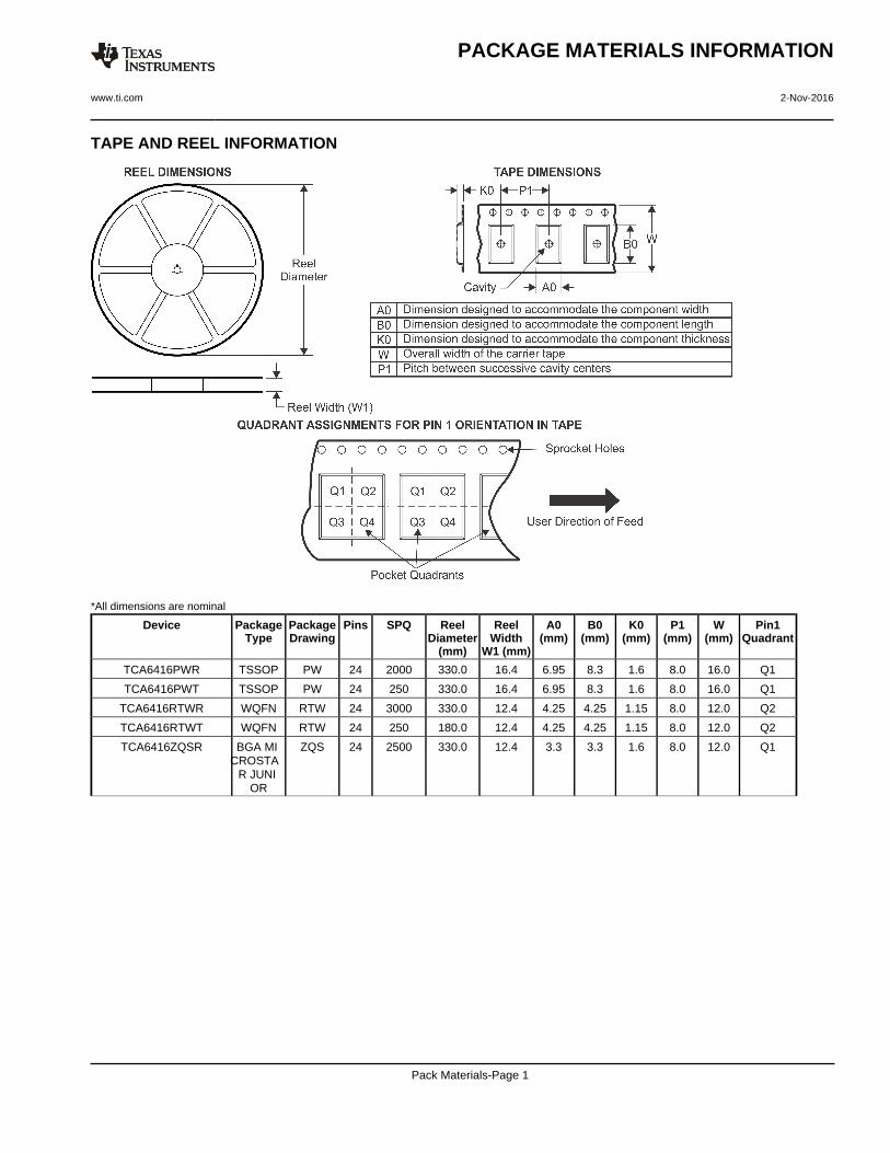
TAPE AND REEL INFORMATION
*All dimensions are nominal
Device PackageType
PackageDrawing
Pins SPQ ReelDiameter
(mm)
ReelWidth
W1 (mm)
A0(mm)
B0(mm)
K0(mm)
P1(mm)
W(mm)
Pin1Quadrant
TCA6416PWR TSSOP PW 24 2000 330.0 16.4 6.95 8.3 1.6 8.0 16.0 Q1
TCA6416PWT TSSOP PW 24 250 330.0 16.4 6.95 8.3 1.6 8.0 16.0 Q1
TCA6416RTWR WQFN RTW 24 3000 330.0 12.4 4.25 4.25 1.15 8.0 12.0 Q2
TCA6416RTWT WQFN RTW 24 250 180.0 12.4 4.25 4.25 1.15 8.0 12.0 Q2
TCA6416ZQSR BGA MI CROSTA
R JUNI OR
ZQS 24 2500 330.0 12.4 3.3 3.3 1.6 8.0 12.0 Q1
PACKAGE MATERIALS INFORMATION
www.ti.com 2-Nov-2016
Pack Materials-Page 1
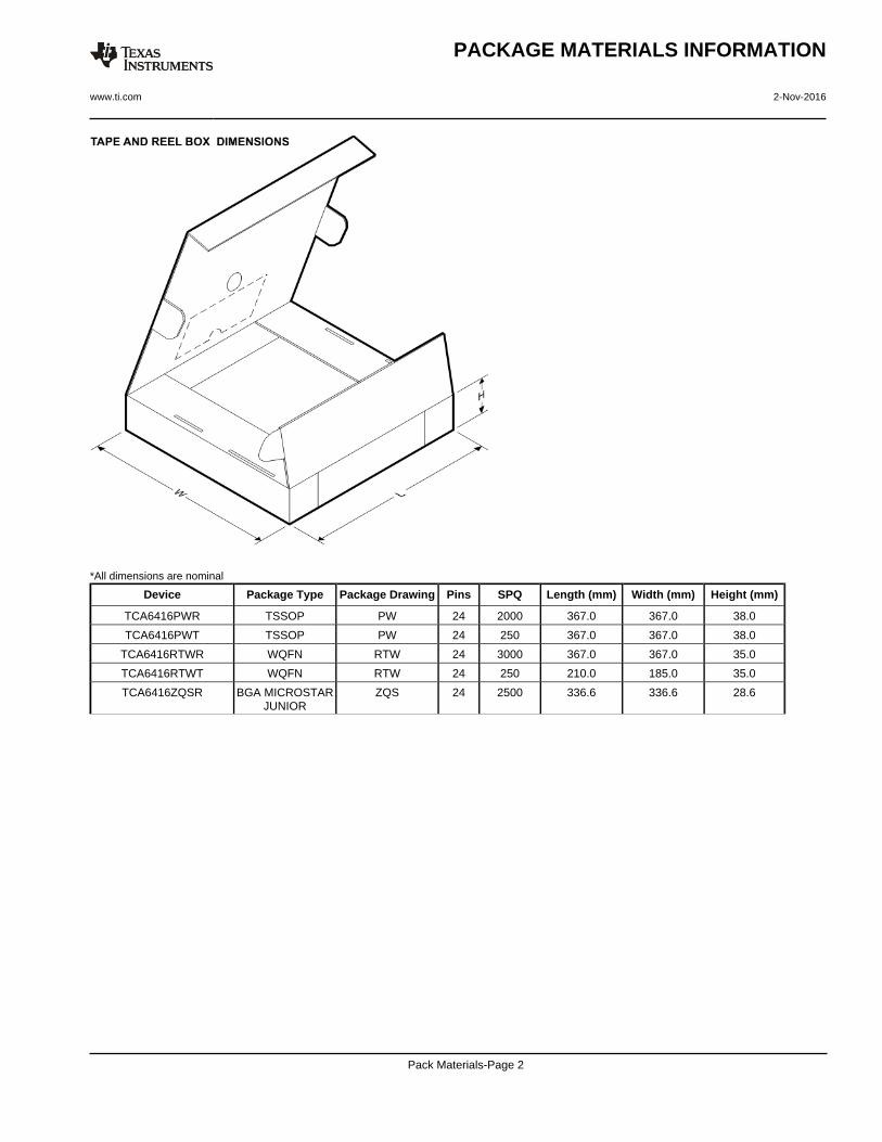
*All dimensions are nominal
Device Package Type Package Drawing Pins SPQ Length (mm) Width (mm) Height (mm)
TCA6416PWR TSSOP PW 24 2000 367.0 367.0 38.0
TCA6416PWT TSSOP PW 24 250 367.0 367.0 38.0
TCA6416RTWR WQFN RTW 24 3000 367.0 367.0 35.0
TCA6416RTWT WQFN RTW 24 250 210.0 185.0 35.0
TCA6416ZQSR BGA MICROSTARJUNIOR
ZQS 24 2500 336.6 336.6 28.6
PACKAGE MATERIALS INFORMATION
www.ti.com 2-Nov-2016
Pack Materials-Page 2
NOTES:
1. All linear dimensions are in millimeters. Any dimensions in parenthesis are for reference only. Dimensioning and tolerancingper ASME Y14.5M.
2. This drawing is subject to change without notice.
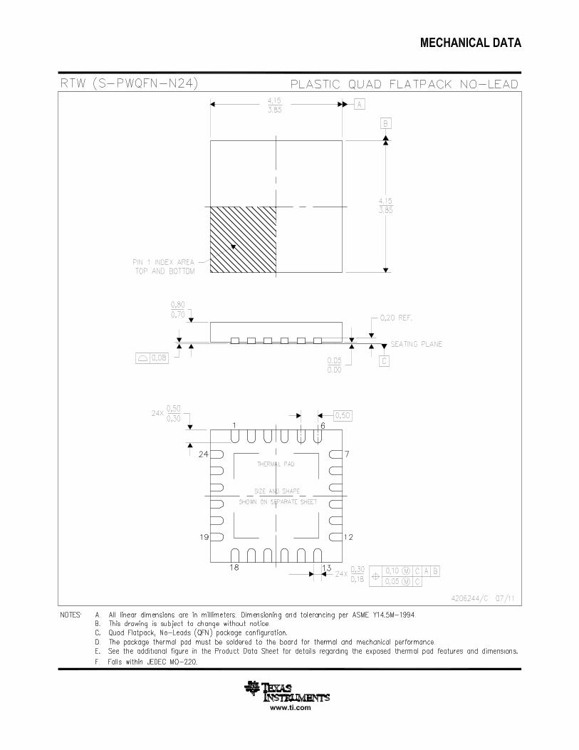
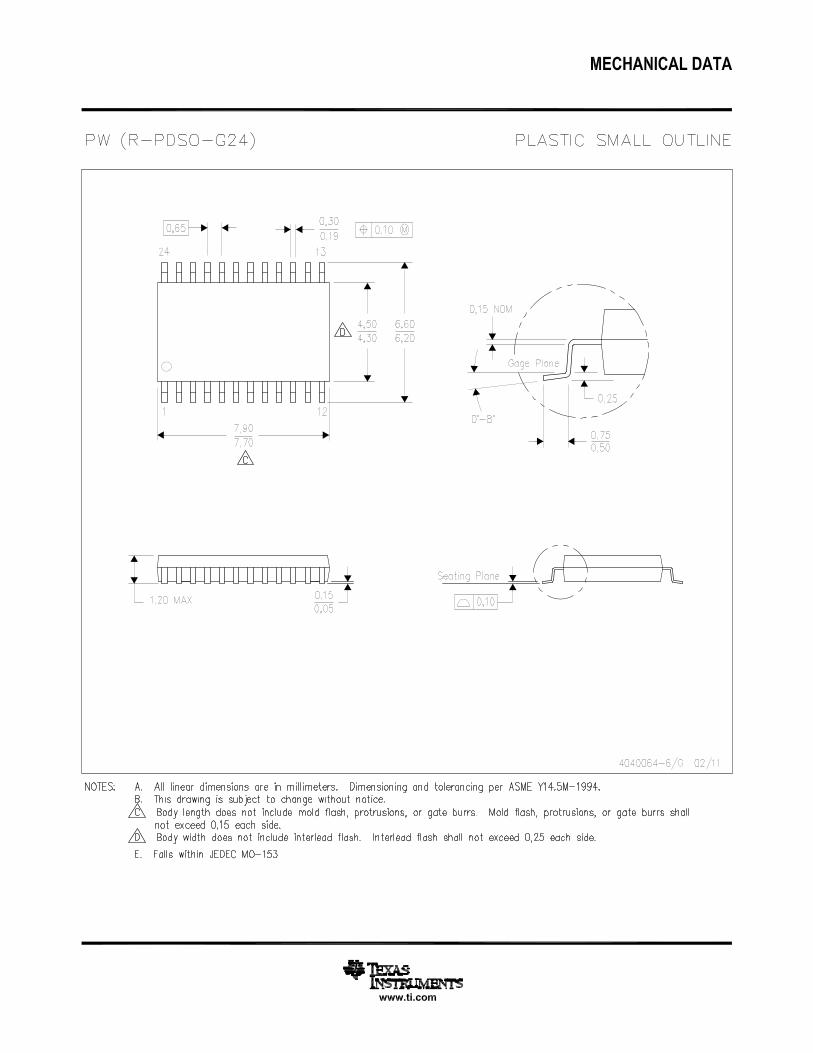
PACKAGE OUTLINE
4219135/A 11/2016
www.ti.com
WQFN - 0.8 mm max height
PLASTIC QUAD FLATPACK-NO LEAD
RTW0024B
A
0.08 C
0.1 C A B0.05 C
B
SYMM
SYMM
4.13.9
4.13.9
PIN 1 INDEX AREA
0.8 MAX
0.050.00
C
SEATING PLANE
PIN 1 ID(OPTIONAL)
2X2.5
20X 0.5
2X 2.5
1
6
18
13
7 12
24 19
2.45±0.1
24X 0.340.24
24X 0.50.3
(0.2) TYP
25
EXPOSEDTHERMAL PAD
NOTES: (continued)
3. For more information, see Texas Instruments literature number SLUA271 (www.ti.com/lit/slua271) .
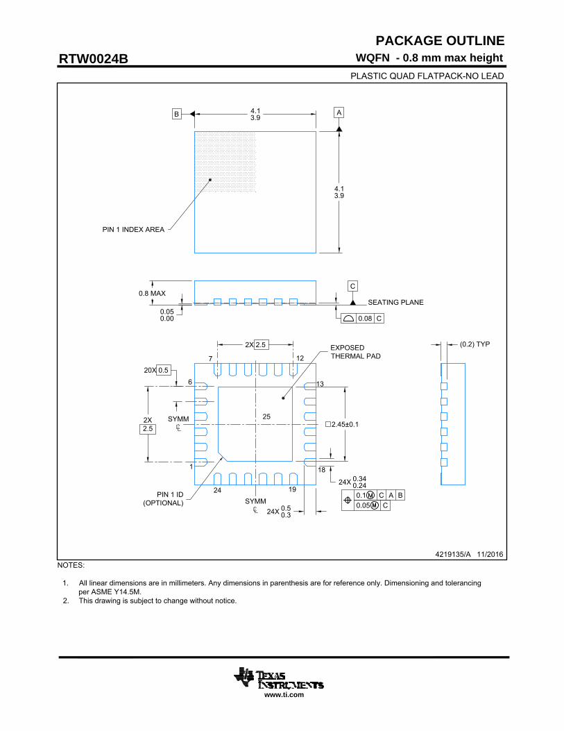
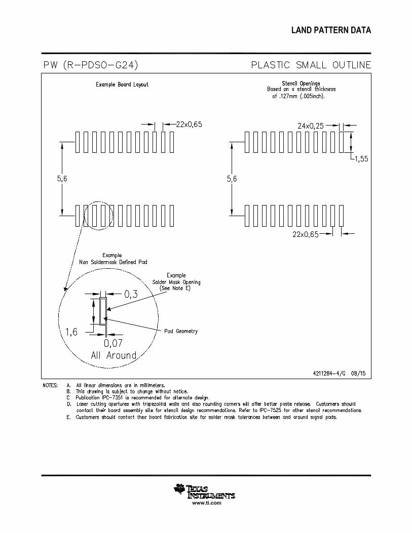
EXAMPLE BOARD LAYOUT
4219135/A 11/2016
www.ti.com
WQFN - 0.8 mm max height
RTW0024B
PLASTIC QUAD FLATPACK-NO LEAD
SYMM
SYMM
LAND PATTERN EXAMPLESCALE: 20X
( 2.45)
24X (0.6)
24X (0.24)1
6
7 12
13
18
1924
(3.8)
(0.97)
(3.8)
(0.97)
25
(R0.05) TYP
20X (0.5)
(Ø0.2) TYPVIA
0.07 MAXALL AROUND 0.07 MIN
ALL AROUNDMETAL
SOLDER MASKOPENING
SOLDER MASKOPENING
METAL UNDERSOLDER MASK
SOLDER MASK DETAILS
NON SOLDER MASKDEFINED
(PREFERRED)SOLDER MASK
DEFINED
NOTES: (continued)
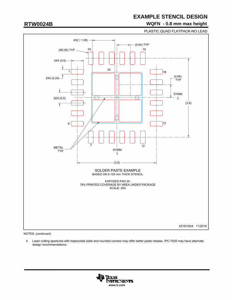
4. Laser cutting apertures with trapezoidal walls and rounded corners may offer better paste release. IPC-7525 may have alternatedesign recommendations.
EXAMPLE STENCIL DESIGN
4219135/A 11/2016
www.ti.com
WQFN - 0.8 mm max height
RTW0024B
PLASTIC QUAD FLATPACK-NO LEAD
SYMM
SYMM
SOLDER PASTE EXAMPLEBASED ON 0.125 mm THICK STENCIL
EXPOSED PAD 25:78% PRINTED COVERAGE BY AREA UNDER PACKAGE
SCALE: 20X
(3.8)
(0.64) TYP
1
6
7 12
13
18
1924
25
(0.64) TYP
4X( 1.08)
(R0.05) TYP
(3.8)
20X (0.5)
24X (0.24)
24X (0.6)
METALTYP
IMPORTANT NOTICE
Texas Instruments Incorporated (TI) reserves the right to make corrections, enhancements, improvements and other changes to itssemiconductor products and services per JESD46, latest issue, and to discontinue any product or service per JESD48, latest issue. Buyersshould obtain the latest relevant information before placing orders and should verify that such information is current and complete.TI’s published terms of sale for semiconductor products (http://www.ti.com/sc/docs/stdterms.htm) apply to the sale of packaged integratedcircuit products that TI has qualified and released to market. Additional terms may apply to the use or sale of other types of TI products andservices.Reproduction of significant portions of TI information in TI data sheets is permissible only if reproduction is without alteration and isaccompanied by all associated warranties, conditions, limitations, and notices. TI is not responsible or liable for such reproduceddocumentation. Information of third parties may be subject to additional restrictions. Resale of TI products or services with statementsdifferent from or beyond the parameters stated by TI for that product or service voids all express and any implied warranties for theassociated TI product or service and is an unfair and deceptive business practice. TI is not responsible or liable for any such statements.Buyers and others who are developing systems that incorporate TI products (collectively, “Designers”) understand and agree that Designersremain responsible for using their independent analysis, evaluation and judgment in designing their applications and that Designers havefull and exclusive responsibility to assure the safety of Designers' applications and compliance of their applications (and of all TI productsused in or for Designers’ applications) with all applicable regulations, laws and other applicable requirements. Designer represents that, withrespect to their applications, Designer has all the necessary expertise to create and implement safeguards that (1) anticipate dangerousconsequences of failures, (2) monitor failures and their consequences, and (3) lessen the likelihood of failures that might cause harm andtake appropriate actions. Designer agrees that prior to using or distributing any applications that include TI products, Designer willthoroughly test such applications and the functionality of such TI products as used in such applications.TI’s provision of technical, application or other design advice, quality characterization, reliability data or other services or information,including, but not limited to, reference designs and materials relating to evaluation modules, (collectively, “TI Resources”) are intended toassist designers who are developing applications that incorporate TI products; by downloading, accessing or using TI Resources in anyway, Designer (individually or, if Designer is acting on behalf of a company, Designer’s company) agrees to use any particular TI Resourcesolely for this purpose and subject to the terms of this Notice.TI’s provision of TI Resources does not expand or otherwise alter TI’s applicable published warranties or warranty disclaimers for TIproducts, and no additional obligations or liabilities arise from TI providing such TI Resources. TI reserves the right to make corrections,enhancements, improvements and other changes to its TI Resources. TI has not conducted any testing other than that specificallydescribed in the published documentation for a particular TI Resource.Designer is authorized to use, copy and modify any individual TI Resource only in connection with the development of applications thatinclude the TI product(s) identified in such TI Resource. NO OTHER LICENSE, EXPRESS OR IMPLIED, BY ESTOPPEL OR OTHERWISETO ANY OTHER TI INTELLECTUAL PROPERTY RIGHT, AND NO LICENSE TO ANY TECHNOLOGY OR INTELLECTUAL PROPERTYRIGHT OF TI OR ANY THIRD PARTY IS GRANTED HEREIN, including but not limited to any patent right, copyright, mask work right, orother intellectual property right relating to any combination, machine, or process in which TI products or services are used. Informationregarding or referencing third-party products or services does not constitute a license to use such products or services, or a warranty orendorsement thereof. Use of TI Resources may require a license from a third party under the patents or other intellectual property of thethird party, or a license from TI under the patents or other intellectual property of TI.TI RESOURCES ARE PROVIDED “AS IS” AND WITH ALL FAULTS. TI DISCLAIMS ALL OTHER WARRANTIES ORREPRESENTATIONS, EXPRESS OR IMPLIED, REGARDING RESOURCES OR USE THEREOF, INCLUDING BUT NOT LIMITED TOACCURACY OR COMPLETENESS, TITLE, ANY EPIDEMIC FAILURE WARRANTY AND ANY IMPLIED WARRANTIES OFMERCHANTABILITY, FITNESS FOR A PARTICULAR PURPOSE, AND NON-INFRINGEMENT OF ANY THIRD PARTY INTELLECTUALPROPERTY RIGHTS. TI SHALL NOT BE LIABLE FOR AND SHALL NOT DEFEND OR INDEMNIFY DESIGNER AGAINST ANY CLAIM,INCLUDING BUT NOT LIMITED TO ANY INFRINGEMENT CLAIM THAT RELATES TO OR IS BASED ON ANY COMBINATION OFPRODUCTS EVEN IF DESCRIBED IN TI RESOURCES OR OTHERWISE. IN NO EVENT SHALL TI BE LIABLE FOR ANY ACTUAL,DIRECT, SPECIAL, COLLATERAL, INDIRECT, PUNITIVE, INCIDENTAL, CONSEQUENTIAL OR EXEMPLARY DAMAGES INCONNECTION WITH OR ARISING OUT OF TI RESOURCES OR USE THEREOF, AND REGARDLESS OF WHETHER TI HAS BEENADVISED OF THE POSSIBILITY OF SUCH DAMAGES.Unless TI has explicitly designated an individual product as meeting the requirements of a particular industry standard (e.g., ISO/TS 16949and ISO 26262), TI is not responsible for any failure to meet such industry standard requirements.Where TI specifically promotes products as facilitating functional safety or as compliant with industry functional safety standards, suchproducts are intended to help enable customers to design and create their own applications that meet applicable functional safety standardsand requirements. Using products in an application does not by itself establish any safety features in the application. Designers mustensure compliance with safety-related requirements and standards applicable to their applications. Designer may not use any TI products inlife-critical medical equipment unless authorized officers of the parties have executed a special contract specifically governing such use.Life-critical medical equipment is medical equipment where failure of such equipment would cause serious bodily injury or death (e.g., lifesupport, pacemakers, defibrillators, heart pumps, neurostimulators, and implantables). Such equipment includes, without limitation, allmedical devices identified by the U.S. Food and Drug Administration as Class III devices and equivalent classifications outside the U.S.TI may expressly designate certain products as completing a particular qualification (e.g., Q100, Military Grade, or Enhanced Product).Designers agree that it has the necessary expertise to select the product with the appropriate qualification designation for their applicationsand that proper product selection is at Designers’ own risk. Designers are solely responsible for compliance with all legal and regulatoryrequirements in connection with such selection.Designer will fully indemnify TI and its representatives against any damages, costs, losses, and/or liabilities arising out of Designer’s non-compliance with the terms and provisions of this Notice.
Mailing Address: Texas Instruments, Post Office Box 655303, Dallas, Texas 75265Copyright © 2017, Texas Instruments Incorporated