tb-ku-115-quattro hardware user manual - fujitsu.com · tb-ku-115-quattro hardware user manual rev....
TRANSCRIPT

TB-KU-115-QUATTRO Hardware User Manual
1 Rev. 1.0
TB-KU-115-QUATTRO Hardware User Manual
Rev. 1.0

TB-KU-115-QUATTRO Hardware User Manual
2 Rev. 1.0
Revision History Version Date Description Publisher Rev. 0.1 2016/06/17 Initial Release (draft for review) AB/ST Rev. 1.0 2016/07/18 Release ST
TB-KU-115-QUATTRO Hardware User Manual
3 Rev. 1.0
Table of Contents 1. Related Documents and Accessories ........................................................................................ 11 2. Overview .................................................................................................................................... 12 3. Features ..................................................................................................................................... 13 4. Block Diagram ........................................................................................................................... 14 5. External View of the Board ........................................................................................................ 15 6. Board Specifications .................................................................................................................. 16 7. Description of Components ....................................................................................................... 18
7.1. Power Supply Structure ........................................................................................................... 18 7.1.1. Power Sequencing .......................................................................................................... 19 7.1.2. Power Input connectors ................................................................................................... 19 7.1.3. DC 6-pin Header and Binding Posts................................................................................ 20 7.1.4. Voltage Rails Test Points ................................................................................................. 21 7.1.5. Power and Miscellaneous LEDs ...................................................................................... 22 7.1.6. Power Switch ................................................................................................................... 23 7.1.7. FPGA/FMC VADJ Voltage Selection ............................................................................... 23
7.2. FPGA Bank Architecture .......................................................................................................... 25 7.2.1. FMC_1 Transceiver Multi-Lane Protocol Limitation ......................................................... 25
7.3. Clock Sub-System ................................................................................................................... 26 7.3.1. FPGA Core Clock Sub-System ........................................................................................ 26 7.3.2. FMC Clock Sub-System .................................................................................................. 26
7.4. FMC Connector Interface ........................................................................................................ 30 7.4.1. FMC Port Ordering .......................................................................................................... 30 7.4.2. Double Width FMC Support ............................................................................................. 31 7.4.3. FMC Pin Assignment ....................................................................................................... 31 7.4.4. FMC Port Implementation Detail: Power, FMC SCL/SDA, GA0/GA1, TDI/TDO ............. 32 7.4.5. FMC0 (J1) Pin Assignment .............................................................................................. 33 7.4.6. FMC1 (J2) Pin Assignment .............................................................................................. 40 7.4.7. FMC2 (J5) Pin Assignment .............................................................................................. 47 7.4.8. FMC3 (J8) Pin Assignment .............................................................................................. 54
7.5. DDR4 SDRAM ......................................................................................................................... 61 7.6. SFP+ Connector ...................................................................................................................... 62 7.7. I2C Sub-System ....................................................................................................................... 63 7.8. USB to UART Controller (FPGA) ............................................................................................. 64 7.9. Battery ..................................................................................................................................... 66 7.10. FPGA Configuration ............................................................................................................. 67
7.10.1. Dual Quad (x8) SPI Flash ................................................................................................ 67 7.10.2. JTAG Programming via 14-pin Header/Digilent® JTAG-over-USB ................................. 69
7.11. General Purpose LEDs (FPGA) .............................................................................................. 70 7.12. General Purpose Switches .................................................................................................. 72
7.12.1. DIP Switches ................................................................................................................... 72 7.12.2. Push Switches ................................................................................................................. 72 7.12.3. Jumper Switches ............................................................................................................. 73
7.13. Zynq Sub-System ................................................................................................................ 75 7.13.1. Connectivity ..................................................................................................................... 76 7.13.2. Power-On Reset and Jumper-based Configuration ........................................................ 78

TB-KU-115-QUATTRO Hardware User Manual
4 Rev. 1.0
8. Appendix .................................................................................................................................... 80 8.1. Default Settings ....................................................................................................................... 80 8.2. Texas Instruments, UCD9090, Power Sequencer ................................................................... 81

TB-KU-115-QUATTRO Hardware User Manual
5 Rev. 1.0
List of Figures Figure 4-1 Block Diagram ................................................................................................................ 14 Figure 5-1 Board Top View ............................................................................................................... 15 Figure 6-1 Board Dimensions (Top Assembly View) ........................................................................ 17 Figure 6-2 Board Dimensions (Bottom Assembly View) .................................................................. 17 Figure 7-1 Power Supply Structure .................................................................................................. 18 Figure 7-2 Power Sequencer ........................................................................................................... 19 Figure 7-3 Power Input Circuit ......................................................................................................... 20 Figure 7-4 12VDC Input Connector and Binding Posts ................................................................... 20 Figure 7-5 Power Switch .................................................................................................................. 23 Figure 7-6 FPGA Banks Assignments .............................................................................................. 25 Figure 7-6 Si5338A Clock Generation .............................................................................................. 26 Figure 7-7 FMC Clock Sub-System Architecture ............................................................................. 27 Figure 7-7 Si5437A, Gigabit Transceiver System ............................................................................ 28 Figure 7-8 SMA Clock/Reference Architecture ................................................................................ 28 Figure 7-8 FMC Port Numbering ...................................................................................................... 30 Figure 7-9 High Pin Count FMC ....................................................................................................... 31 Figure 7-10 FMC_0 - 3 (SCL/SDA, GA0/GA1, TDI/TDO) ................................................................ 32 Figure 7-11 DDR4 SDRAM Structure ............................................................................................... 61 Figure 7-12 SFP+ Cage Location..................................................................................................... 62 Figure 7-12 SFP+ System ................................................................................................................ 62 Figure 7-12 I2C Sub-System ............................................................................................................ 63 Figure 7-13 USB UART Interface (FPGA) ....................................................................................... 65 Figure 7-14 Battery Circuit ............................................................................................................... 66 Figure 7-15 FPGA SPI Flash Configuration Structure ..................................................................... 67 Figure 7-15 Push Button to initiate FPGA reconfiguration ............................................................... 68 Figure 7-15 FPGA/ZYNQ JTAG Header Location ........................................................................... 69 Figure 7-15 FPGA/ZYNQ JTAG Chain Architecture ........................................................................ 70 Figure 7-15 LED drive circuit ............................................................................................................ 71 Figure 7-15 LED Location ................................................................................................................ 71 Figure 7-15 DIP Switch Location ...................................................................................................... 72 Figure 7-15 Push Button Switch Location ........................................................................................ 73 Figure 7-16 Jumper Switches Structure ........................................................................................... 73 Figure 7-16 Jumper Switches Location ............................................................................................ 74 Figure 7-16 Zynq Sub-System Architecture ..................................................................................... 75 Figure 7-16 Zynq Sub-System Photo ............................................................................................... 75 Figure 8-1 Default Jumper Positions ................................................................................................ 80 Figure 8-1 UCD9090 Headers ......................................................................................................... 81
TB-KU-115-QUATTRO Hardware User Manual
6 Rev. 1.0
List of Tables Table 6-1 Board Specifications ......................................................................................................... 16 Table 7-1 Voltage Rail Test Points .................................................................................................... 21 Table 7-2 Board Power & Configuration LEDs ................................................................................. 22 Table 7-3 Board User-Defined LEDs ................................................................................................ 22 Table 7-4 FMC[0] voltage selection, J57 .......................................................................................... 24 Table 7-5 FMC[3:1] voltage selection, J56 ....................................................................................... 24 Table 7-2 SMA Clock and Reference Ports ...................................................................................... 29 Table 7-2 FMC Port I/O Support ....................................................................................................... 30 Table 7-2 FMC Over-Current Protection PTCs ................................................................................ 32 Table 7-6 FMC0 (J1) to FPGA Pinout (Rows A-B) ........................................................................... 34 Table 7-7 FMC 0 (J1) to FPGA Pinout (Rows C-D) .......................................................................... 35 Table 7-8 FMC 0 (J1) to FPGA Pinout (Rows E-F) .......................................................................... 36 Table 7-9 FMC 0 (J1) to FPGA Pinout (Rows G-H) ......................................................................... 37 Table 7-10 FMC 0 (J1) to FPGA Pinout (Rows J-K) ......................................................................... 38 Table 7-11 FMC 1 (J2) to FPGA Pinout (Rows A-B) ........................................................................ 41 Table 7-12 FMC 1 (J2) to FPGA Pinout (Rows C-D) ........................................................................ 42 Table 7-13 FMC 1 (J2) to FPGA Pinout (Rows E-F) ........................................................................ 43 Table 7-14 FMC 1 (J2) to FPGA Pinout (Rows G-H) ....................................................................... 44 Table 7-15 FMC 1 (J2) to FPGA Pinout (Rows J-K) ......................................................................... 45 Table 7-16 FMC 2 (J5) to FPGA Pinout (Rows A-B) ........................................................................ 48 Table 7-17 FMC 2 (J5) to FPGA Pinout (Rows C-D) ........................................................................ 49 Table 7-18 FMC 2 (J5) to FPGA Pinout (Rows E-F) ........................................................................ 50 Table 7-19 FMC 2 (J5) to FPGA Pinout (Rows G-H) ....................................................................... 51 Table 7-20 FMC 2 (J5) to FPGA Pinout (Rows J-K) ......................................................................... 52 Table 7-21 FMC 3 (J8) to FPGA Pinout (Rows A-B) ........................................................................ 55 Table 7-22 FMC 3 (J8) to FPGA Pinout (Rows C-D) ........................................................................ 56 Table 7-23 FMC 3 (J8) to FPGA Pinout (Rows E-F) ........................................................................ 57 Table 7-24 FMC 3 (J8) to FPGA Pinout (Rows G-H) ....................................................................... 58 Table 7-25 FMC 3 (J8) to FPGA Pinout (Rows J-K) ......................................................................... 59 Table 7-27 SFP+ Ctrl/Status Pin Assignments ................................................................................. 62 Table 7-26 I2C Bus Pin Assignment (FPGA) .................................................................................... 63 Table 7-26 I2C Devices and Addresses ............................................................................................ 64 Table 7-28 Micro-USB Type B and AB Compatibility ....................................................................... 64 Table 7-29 UART Interface Pin Assignment ..................................................................................... 65 Table 7-30 SPI Flash Memory Pin Assignment ................................................................................ 68 Table 7-31 Xilinx 14-pin JTAG Pinout ............................................................................................... 70 Table 7-32 FPGA Bank 0 JTAG Pin Assignment .............................................................................. 70 Table 7-33 Uncommitted LEDs Pin Assignment .............................................................................. 71 Table 7-34 DIP Switches Pin Assignment ........................................................................................ 72 Table 7-35 Push-button Switches Pin Assignment ........................................................................... 72 Table 7-36 Jumper Switches Pin Assignment .................................................................................. 73 Table 7-29 Zynq QSPI Pin Assignment ............................................................................................ 76 Table 7-29 Zynq uSD Pin Assignment.............................................................................................. 76 Table 7-29 Zynq PL JTAG Header Pin Assignment ......................................................................... 77 Table 7-29 Zynq UART Pin Assignment ........................................................................................... 77

TB-KU-115-QUATTRO Hardware User Manual
7 Rev. 1.0
Table 7-29 Zynq GP DIP Switch Pin Assignment ............................................................................. 77 Table 7-29 Zynq GP LED Pin Assignment ....................................................................................... 77 Table 7-29 Zynq I2C Pin Assignment ................................................................................................ 78 Table 7-29 Zynq GPIO Pin Assignment ............................................................................................ 78 Table 7-36 Zynq Boot Mode Configuration....................................................................................... 79

TB-KU-115-QUATTRO Hardware User Manual
8 Rev. 1.0
Introduction Thank you for purchasing the TB-KU-115-QUATTRO board. Before using the product, be sure to carefully read this user manual and fully understand how to correctly use the product. First read through this manual, and always keep it handy.
SAFETY PRECAUTIONS Be sure to follow these precautions Observe the precautions listed below to prevent injuries to you or other personnel or damage to property. • Before using the product, read these safety precautions carefully to ensure proper use. • These precautions contain serious safety instructions that must be followed. • After reading through this manual, be sure to always keep it handy. The following conventions are used to indicate the possibility of injury/damage and classify precautions if the product is handled incorrectly.
Indicates the high possibility of serious injury or death if the product is handled incorrectly.
Indicates the possibility of serious injury or death if the product is handled incorrectly.
Indicates the possibility of injury or physical damage in connection with houses or household goods if the product is handled incorrectly.
The following graphical symbols are used to indicate and classify precautions in this manual. (Examples)
Turn off the power switch.
Do not disassemble the product.
Do not attempt this.
Danger
Warning
Caution
!

TB-KU-115-QUATTRO Hardware User Manual
9 Rev. 1.0
In the event of a failure, disconnect the power supply. If the product is used as is, a fire or electric shock may occur. Disconnect the power supply immediately and contact our sales personnel for repair.
If an unpleasant smell or smoking occurs, disconnect the power supply. If the product is used as is, a fire or electric shock may occur. Disconnect the power supply immediately. After verifying that no smoking is observed, contact our sales personnel for repair.
Do not disassemble, repair or modify the product. Otherwise, a fire or electric shock may occur due to a short circuit or heat generation. For inspection, modification or repair, contact our sales personnel.
Do not touch a cooling fan. As a cooling fan rotates in high speed, do not put your hand close to it. Otherwise, it may cause injury to persons. Never touch a rotating cooling fan.
Do not place the product on unstable locations. Otherwise, it may drop or fall, resulting in injury to persons or failure.
If the product is dropped or damaged, do not use it as is. Otherwise, a fire or electric shock may occur.
Do not touch the product with a metallic object. Otherwise, a fire or electric shock may occur.
Do not place the product in dusty or humid locations or where water may
splash. Otherwise, a fire or electric shock may occur.
Do not get the product wet or touch it with a wet hand. Otherwise, the product may break down or it may cause a fire, smoking or electric shock.
Do not touch a connector on the product (gold-plated portion). Otherwise, the surface of a connector may be contaminated with sweat or skin oil, resulting in contact failure of a connector or it may cause a malfunction, fire or electric shock due to static electricity.
Warning
!
!
!
!
!
!
!

TB-KU-115-QUATTRO Hardware User Manual
10 Rev. 1.0
Do not use or place the product in the following locations. • Humid and dusty locations • Airless locations such as closet or bookshelf • Locations which receive oily smoke or steam • Locations exposed to direct sunlight • Locations close to heating equipment • Closed inside of a car where the temperature becomes high • Staticky locations • Locations close to water or chemicals Otherwise, a fire, electric shock, accident or deformation may occur due to a short circuit or heat generation.
Do not place heavy things on the product. Otherwise, the product may be damaged.
■ Disclaimer This product is an evaluation board intended for development of video data with Xilinx Kintex UltraScale FPGA.
Tokyo Electron Device Limited assumes no responsibility for any damages resulting from the use of this product for
purposes other than those stated.
Even if the product is used properly, Tokyo Electron Device Limited assumes no responsibility for any damages
caused by:
(1) Earthquake, thunder, natural disaster or fire resulting from the use beyond our responsibility, acts by a third
party or other accidents, the customer’s willful or accidental misuse or use under other abnormal conditions.
(2) Secondary impact arising from use of this product or its unusable state (business interruption or others)
(3) Use of this product against the instructions given in this manual.
(4) Malfunctions due to connection to other devices.
Tokyo Electron Device Limited assumes no responsibility or liability for:
(1) Erasure or corruption of data arising from use of this product.
(2) Any consequences or other abnormalities arising from use of this product, or
(3) Damage of this product not due to our responsibility or failure due to modification
This product has been developed by assuming its use for research, testing or evaluation. It is not authorized for use
in any system or application that requires high reliability.
Repair of this product is carried out by replacing it on a chargeable basis, not repairing the faulty devices.
However, non-chargeable replacement is offered for initial failure if such notification is received within two weeks
after delivery of the product.
The specification of this product is subject to change without prior notice.
The product is subject to discontinuation without prior notice.
Caution
!
!

TB-KU-115-QUATTRO Hardware User Manual
11 Rev. 1.0
1. Related Documents and Accessories Related documents: All documents relating to this board can be downloaded from our website. Please see attached paper on the products. Xilinx FPGA document: http://www.xilinx.com/support/index.html/content/xilinx/en/supportNav/silicon_devices/fpga/kintex-ultrascale.html DS892: UltraScale device data sheets: Kintex UltraScale Architecture Data Sheet: DC and AC Switching Characteristics DS890: UltraScale Architecture and Product Overview UG570: UltraScale Architecture Configuration User Guide UG571: UltraScale Architecture SelectIO Resources User Guide UG572: UltraScale Architecture Clocking Resources User Guide UG573: UltraScale Architecture Memory Resources User Guide UG574: UltraScale Architecture Configurable Logic Block User Guide UG575: UltraScale Architecture Packaging and Pinouts User Guide UG576: UltraScale Architecture GTH Transceivers User Guide UG580: UltraScale Architecture System Monitor User Guide UG583: UltraScale Architecture PCB and Pin Planning User Guide PG150: UltraScale Architecture-Based Memory Interface Solutions Product Guide Board accessories: - Power supply brick (DC 12V) and cable to board: qty. 1 - FMC spacer set
Standoff 2.6M x 30mm qty. 14 Screw 2.6M x 6mm qty.14
- Power Strip Cord with Individual Switches qty. 1

TB-KU-115-QUATTRO Hardware User Manual
12 Rev. 1.0
2. Overview The TB-KU-115-QUATTRO “Quattro” development board enables users to evaluate, experiment, build, and target designs destined for the Xilinx Kintex UltraScale (US) FPGA. Quattro features a Kintex US 115, -2 speed grade FPGA, in an FLVA1517 package. The Quattro platform is also provisioned with a several peripherals and expansion ports (e.g. FMCs). The combination of a large Kintex US FPGA and a carefully selected list of peripherals, makes Quattro a flexible solution for jump starting your FPGA design, and de-risking your entire development program.
TB-KU-115-QUATTRO Hardware User Manual
13 Rev. 1.0
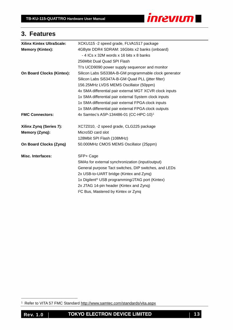
3. Features Xilinx Kintex UltraScale: XCKU115 -2 speed grade, FLVA1517 package Memory (Kintex): 4GByte DDR4 SDRAM: 16Gbits x2 banks (onboard)
- 4 ICs x 32M words x 16 bits x 8 banks 256Mbit Dual Quad SPI Flash TI’s UCD9090 power supply sequencer and monitor On Board Clocks (Kintex): Silicon Labs Si5338A-B-GM programmable clock generator
Silicon Labs Si5347A-B-GM Quad PLL (jitter filter) 156.25MHz LVDS MEMS Oscillator (50ppm) 4x SMA differential pair external MGT XCVR clock inputs 1x SMA differential pair external System clock inputs
1x SMA differential pair external FPGA clock inputs 1x SMA differential pair external FPGA clock outputs FMC Connectors: 4x Samtec’s ASP-134486-01 (CC-HPC-10)1 Xilinx Zynq (Series 7): XC7Z010, -2 speed grade, CLG225 package Memory (Zynq): MicroSD card slot 128Mbit SPI Flash (108MHz) On Board Clocks (Zynq) 50.000MHz CMOS MEMS Oscillator (25ppm) Misc. Interfaces: SFP+ Cage SMAs for external synchronization (input/output) General purpose Tact switches, DIP switches, and LEDs 2x USB-to-UART bridge (Kintex and Zynq) 1x Digilent® USB programming/JTAG port (Kintex) 2x JTAG 14-pin header (Kintex and Zynq) I2C Bus, Mastered by Kintex or Zynq
1 Refer to VITA 57 FMC Standard http://www.samtec.com/standards/vita.aspx

TB-KU-115-QUATTRO Hardware User Manual
14 Rev. 1.0
4. Block Diagram XCKU115:
• All four FMC connectors have 10 high-speed GTH lanes2 • FMC0 has 34 LA LVDS pairs and 5 HA LVDS pairs • FMC1 has 34 LA LVDS pairs • FMC2 has 19 LA LVDS pairs and 10 LA LVCMOS (single-ended) • FMC3 has 34 LA LVDS pairs
KINTEXULTRASCALE
FPGA(060, 085 or 115)
IOExpander
IOExpander
I2CMUX
FMC 0
FMC 1
FMC 2
FMC 3
USB to UART
USB
CLOCKGENERATOR
(Si5338)
QUAD PLL(Si5347)
25MhzXTAL
USB to UARTQSPI FLASH
OOOOOOOO
SMA GTH CLOCK INPUTS
JTAG
PWR
12V IN
VCCINTDC-DC
POWERSEQUENCER
3V3LDO
VCCINTDC-DC
1V0 MGTDC-DC
1V8 VCC AUX
DC-DC
1V2 VTTDC-DC
1V8 MGT AUXLDO
FMC0 VADJ
DC-DC
FMC1,2,3 VADJ
DC-DC
3V3DC-DC
1V2 DDR4DC-DC
DDR4 1 TERMLDO
DDR4 2TERMLDO
0V951V0MGT
1V8AUX
1V2MGT
VADJ0
VADJ1
1V2DDR
1V8MGT
3V3
0V6VTT1
0V6VTT2
12V
VADJ_SELECT
12V_SENS0V95_SENS
1V8_VCCAUX_SENS1V0_MGTAVCC_SENS1V2_MGTAVTT_SENS
3V3_HR_VADJ_FMC0_SENS1V8_VADJ_FMC123_SENS
3V3_SENS2V5_DDR4
1V2_DDR4_SENS
3V3_SEQ
0V95_EN1V8_VCCAUX_EN1V0_MGTAVCC_EN1V2_MGTAVTT_EN1V8_MGTVCCAUX_EN3V3_HR_VADJ_FMC0_EN1V8_VADJ_FMC123_EN3V3_EN2V5_DDR4_EN1V2_DDR4_EN
PWR_UP_PROG_NPWRUP_HOLD_PLS
FMC[3:0]_PGOOD
PWRUP_HOLD_PLS
FMC0_PGOOD
FMC1_PGOOD
FMC2_PGOOD
FMC3_PGOOD
FMC0_PRES_NFMC0_PGOOD_M2C
FMC1_PRES_NFMC1_PGOOD_M2C
FMC2_PRES_NFMC2_PGOOD_M2C
FMC3_PRES_NFMC3_PGOOD_M2C
FMC3_PRES_NFMC3_PGOOD_M2C
FMC2_PRES_NFMC2_PGOOD_M2C
FMC1_PRES_NFMC1_PGOOD_M2C
FMC0_PRES_NFMC0_PGOOD_M2C
FMC0_GTH[9:0]_P/N
I2C_
MUX
_RST
N
FPGA
_IO
_I2C
I2C_
DEVI
CE_I
NT_N
INT_NINT_N
TIMING_I2C
CLK_EXT_REF
UART
(Rx,
Tx,C
TS,R
TS)
FMC0_LA[33:0]_P/N
FMC0_HA[5:0]_P/N
FMC0_GTH_M2C_CLK[1:0]_P/N
FMC0_M2C_CLK[1:0]_P/N
FMC1_GTH_M2C_CLK[1:0]_P/N
FMC1_M2C_CLK[1:0]_P/N
FMC2_GTH_M2C_CLK[1:0]_P/N
FMC2_M2C_CLK[1:0]_P/N
FMC3_GTH_M2C_CLK[1:0]_P/N
FMC3_M2C_CLK[1:0]_P/N
FMC1_GTH[9:0]_P/N
FMC1_LA[33:0]_P/N
FMC2_GTH[9:0]_P/N
FMC3_GTH[9:0]_P/N
FMC3_LA[33:0]_P/N
FMC2_LA[18:0]_P/N
FMC2_LA[26:19]_P/N (SINGLE ENDED ONLY)
HR BANKS 64,65
GTH BANKS224,225,226
HP BANKS 44,45
HP BANKS24,44,45
HP BANKS24,25
GTH BANKS227,228,229
GTH BANKS126,127,128
GTH BANKS230,231,232
HP BANKS66,67,6846,47,48
HR BANKS 0,64,65
FMC0_REC_CLKQUAD_PLL_OE_NQUAD_PLL_RST_NQUAD_PLL_INT_N
QUAD_PLL_LOL[3:0]FMC1_REC_CLK
FMC2_REC_CLK
FMC3_REC_CLK
FMC0_REC_CLK
FMC1_REC_CLK
FMC2_REC_CLK
FMC3_REC_CLK
QUAD_PLL_OE_NQUAD_PLL_RST_NQUAD_PLL_INT_N
QUAD_PLL_LOL[3:0]
SI5338_INTR
100MHZ_CLK200MHZ_CLK1200MHZ_CLK2
50M
HZ_C
LK
FMC0_REF_CLK_PLLFMC1_REF_CLK_PLLFMC2_REF_CLK_PLLFMC3_REF_CLK_PLL
QUAD224_REF_CLKQUAD230_REF_CLKQUAD231_REF_CLKQUAD126_REF_CLK
SWITCHES ANDLEDS
VADJ = 1.8, 2.5 or 3.3V
VADJ = 1.5V or 1.8V(common for FMC1,2,3)
10 GTH Transcievers
10 GTH Transcievers (085, 115)8 GTH Transcievers (060)
10 GTH Transcievers
10 GTH Transcievers (085, 115)0 GTH Transcievers (060)
FMC LA (34 Pairs)FMC HA (6 Pairs)
FMC LA (34 Pairs)
FMC LA (18 Pairs)FMC LA (16 Single Ended)
FMC LA (34 Pairs)
VADJ = 1.5V or 1.8V(common for FMC1,2,3)
VADJ = 1.5V or 1.8V(common for FMC1,2,3)
FMC_I2C
USB to UARTDDR4 SRAM
Digilent USB to JTAG
SFP+SFP+_CTRL/STATUS
SFP+_CTRL/STATUS
OOSMA Ext. Sys_Clk input
OOSMA Ext. FPGA Sync Clock
Figure 4-1 Block Diagram
2 Note: Due to the SSI technology employed within the 115 device, FMC1’s transceivers are limited to at most an 8+2 lane wide GTH protocol configuration; FMC0, 2, & 3 can implement 10-lane GTH width protocols

TB-KU-115-QUATTRO Hardware User Manual
15 Rev. 1.0
5. External View of the Board The TB-KU-115-QUATTRO components are shown on the top side view in Figure 5-1.
SFP+Cage
PowerSwitch
Power InputConnector
Power InputBinding Posts
FPGA ProgButton
SequencerPMBUS Header
UncommittedSwitches /Headers /
PushbuttonsDual Quad
Flash Memory
DDR4 SDRAM(2 banks)
FPGA Coin CellBattery Holder
FanConnector
FPGAXilinx® Kintex®
UltraScale™ 115uSD Slot
FPGAUART
FPGAJTAG
Zynq®
UART
Zynq Uncommitted DIP Switches
Xilinx Zynq®
7010
ZynqReset
FMCVADJ
ZynqPL JTAGFPGA/Zynq
JTAG
EXTCLKin
Quad230MGTREFCLK1
Quad227MGTREFCLK1
SI5374AOUT1
EXTSYNC OUT
EXTCLK OUT
EXTSYNC IN
EXTCLKin
Quad126MGTREFCLK1
Quad224MGTREFCLK1Sequencer
JTAG
FMC2VADJ=1.5,1.8
(common FMC1,2,3)GTH=10
LA=19pairs+10se
FMC1VADJ=1.5,1.8
(common FMC1,2,3)GTH=10(8+2 due to SLR)
LA=34pairs
FMC0VADJ=1.8,2.5,3.3
GTH=10LA=34pairsHA=5pairs
FMC3VADJ=1.5,1.8
(common FMC1,2,3)GTH=10
LA=34pairs
Figure 5-1 Board Top View

TB-KU-115-QUATTRO Hardware User Manual
16 Rev. 1.0
6. Board Specifications The table below shows the board specifications.
Table 6-1 Board Specifications External Dimensions: 316.2 mm (W) x 207.2 mm (H) Number of Layers: 20 layers Board Thickness: 2.09 mm +/- 10% Material: Megtron 4 FPGA: Xilinx, Kintex US, XCKU115- 2FLVA1517 FMC HPC Connector: Samtec, ASP-134486-01 Micro-USB Connector: Hirose, ZX62D-AB-5P8 Xilinx JTAG Connector: Molex, 87832-1420 MicroSD Slot: Hirose, DM3BT-DSF-PEJS SFP+ Cage: Molex, 74754-0101 SFP+ Connector: Molex, 744410010 Power Input Connector: Molex, 39-30-1060 Power Input Banana Jacks: Cinch, 111-0702-001 and 111-0703-001

TB-KU-115-QUATTRO Hardware User Manual
17 Rev. 1.0
Figure 6-1 Board Dimensions (Top Assembly View)
Figure 6-2 Board Dimensions (Bottom Assembly View)

TB-KU-115-QUATTRO Hardware User Manual
18 Rev. 1.0
7. Description of Components
7.1. Power Supply Structure TB-KU-115-QUATTRO board’s power supply structure is shown in the figure below.
KCU Vccint 0.95V +/- 3%KCU Vccint_io 0.95V +/- 3%PTH08T250WAZT x2
80A current share KCU Vccbram 0.95V +/- 3%
enable signals
TPS53318KCU Vccaux 1.80V +/- 3%KCU Vccaux_io 1.80V +/- 3%
KCU Vccadc 1.8V +/- 3%
TPS53318 KCU Vcco HR 1.8V/2.5V/3.3V +3/- 5%
TPS53319 KCU Vcco HP 1.5/1.8V +/- 5%
TPS53355 SFP+ module 3.3V +/-3%
TPS53318KCU Vcco DDR4 1.2V +/- 5%DDR4 chip VDDQ, DDR4 VtermZYNQ VCCO
TPS51206Termination 3A
KCU Vterm DDR4 0.6VDDR4 Vterm 0.6V (0.49-0.51VDD) x8
TPS73801 DDR4 chip VPP 2.5V +10/-5% x8
DDR4
TPS53319 KCU Vmgtavcc 1.00V +/- 3% (0.970 to 1.030V)
TPS53319 KCU Vmgtavtt 1.20V +/- 2.5%(1.170 to 1.230V)KCU Vmgtavttrcal 1.20V +/- 2.5%(1.170 to 1.230V)
TPS73801 KCU Vmgtvccaux 1.80V +/- 2.8%(1.750 to 1.850V)
MGTs
FMC0 VADJ
FMC1,2,3 VADJ
3.3V
CORE
FMC0 12V; 1AFMC1 12V; 1AFMC2 12V; 1AFMC3 12V; 1A
LP2992A UCD9090 3V3_UCD9090 3.3V +/-3%
UCD9090Sequencer
PTC
TPS73801 KCU V1v8_USB_PWR_ZYNQ 1.80V +/- 2.8%(1.750 to 1.850V)ZYNQ USB
UART
TPS73801 KCU V1v8_USB_PWR 1.80V +/- 2.8%(1.750 to 1.850V)FPGA USB
UART
LMZ12002 ZYNQ 1V0_zynq_int 1.0V +/-3%
FMC0, 3.3VFMC1, 3.3VFMC2, 3.3VFMC3, 3.3V
FMC1, VADJFMC2, VADJFMC3, VADJ
FMC0, VADJ
12V INPUT CONNECTORS
PTC
Figure 7-1 Power Supply Structure

TB-KU-115-QUATTRO Hardware User Manual
19 Rev. 1.0
7.1.1. Power Sequencing
The UCD9090 chip features power sequencing and monitoring of the different power supplies available on this board. The sequencer’s outputs are connected to the power supplies’ enable pin which activates each device. The connections to the UCD9090 are shown below.
UCD9090RGZ
0V95_EN
1V8_AUX_ZYNQ_INT_EN
1V0_MGTAVCC_EN
1V2_MGTAVTT_EN
1V8_MGTVCCAUX_EN
3V3_HR_VADJ_FMC0_EN
1V8_VADJ_FMC123_EN
3V3_EN
2V5_DDR4_EN
1V2_DDR4_EN
GPIO1
GPIO2
GPIO3
GPIO4
GPIO5
GPIO6
GPIO7
GPIO8
GPIO9
GPIO10
MON1
MON2
MON3
MON4
MON5
MON6
MON7
MON8
MON9
MON10
12V0
0V95_SENS
1V8_VCCAUX_SENS
1V0_MGTAVCC_SENS
1V2_MGTAVTT_SENS
3V3_HR_VADJ_FMC0_SENS
1V8_VADJ_FMC123_SENS
3V3_SENS
2V5_DDR4
1V2_DDR4_SENS
GPIO11AND
All power good
FPGA_PROGRAM_B
Push SwitchReconfiguration
PMBUSCTRL3V3_UCD9090
GPIO12 FMC_[3..0]_PGOOD
Figure 7-2 Power Sequencer The VCCINT power rail is generated by two PTH08T250WAZT current-sharing modules which are interconnected to provide the 0.95V supply required for the Kintex Ultrascale FPGA core.
The power sequencer is discussed in greater detail in 8.2.
7.1.2. Power Input connectors
TB-KU-115-QUATTRO has two means to apply power to the board; via a 6-pin Molex connector or via the red(+) and black(-) binding posts.
NOTE: As shown in the schematic below, the 6-pin Molex connector and the binding posts (banana jacks) are directly connected in parallel. Only apply power from, and only connect to, one source at a time.

TB-KU-115-QUATTRO Hardware User Manual
20 Rev. 1.0
Figure 7-3 Power Input Circuit
7.1.3. DC 6-pin Header and Binding Posts
NOTE: There are two (2) power inputs available on this board. Connect one OR the other 12VDC inputs. NEVER connect both power inputs simultaneously.
Figure 7-4 12VDC Input Connector and Binding Posts

TB-KU-115-QUATTRO Hardware User Manual
21 Rev. 1.0
7.1.4. Voltage Rails Test Points
Use the development board’s power rail test points for board debugging and troubleshooting or for other types of measurements.
Table 7-1 Voltage Rail Test Points Voltage Rail Test Point # Power Supply for
0V95 TP37 FPGA VCCINT 0V95_VCCBRAM TP23 FPGA VCCBRAM
1V8_VCCAUX TP40 FPGA VCCAUX & VCCAUX_IO 3V3_HR_VADJ_FMC0 TP36 FPGA HR I/O Bank FMC0
3V3_UCD9090 TP43 Power Sequencer and Monitor 1V8_VADJ_FMC123 TP103 FPGA HP I/O Banks & FMC VADJ
1V2_DDR4 TP31 DDR4 and corresponding FPGA Banks 2V5_DDR4 TP30 VPP generation
0V6_VTT_DDR4 TP32 DDR4 SDRAM 1 Termination 0V6_VREF_DDR4 TP34 DDR4 SDRAM 1 Reference 0V6_VTT_DDR4_2 TP33 DDR4 SDRAM 2 Termination
0V6_VREF_DDR4_2 TP35 DDR4 SDRAM 2 Reference 1V0_MGTAVCC TP39 FPGA MGTAVCC 1V2_MGTAVTT TP41 FPGA MGTAVTT
1V8_MGTVCCAUX TP38 FPGA MGTVCCAUX 3V3 TP20 FMC and SFP+ modules
12V0 TP42 12V Master Power VBATT TP68 Coin Cell Battery
5V0_USB_VBUS TP57 Micro USB 5V input 5V0_USB_FILT TP59 Micro USB filtered 5V 1V8_USB_PWR TP58 USB UART controller 1.8V I/O
1V8_USB_PWR_ZYNQ TP123 Zynq USB UART Controller 1.8V 5V0_USB_ZYNQ_FILT TP122 Zynq Micro USB filtered 5V
5V0_USB_VBUS_ZYNQ TP124 Zynq USB VBus 5V (external) 1V0_ZYNQ_INT C1021
(capacitor, no
dedicated test point)
Zynq Internal 1.0V

TB-KU-115-QUATTRO Hardware User Manual
22 Rev. 1.0
7.1.5. Power and Miscellaneous LEDs
Shown below are the various LEDs present on the board which serve as configuration and power indication and the general purpose user programmable LEDs.
Table 7-2 Board Power & Configuration LEDs LED Color Used for D56
(KINTEX_CONFIG_DONE) Bicolor:
Red/Green Kintex FPGA Programming DONE signal
Red: Programming in progress or unprogrammed Green: Programming complete
D49 (ZYNQ_CONFIG_DONE)
Bicolor: Red/Green
ZYNQ FPGA Programming DONE signal Red: Programming in progress or unprogrammed
Green: Programming complete D50
(ZYNQ_INIT_LED) Green Zynq INIT signal
Green: ZYNQ_INIT_N released D10 Green 12V Input
Green: Sufficient voltage is available at the 12V input to enable the LED
Table 7-3 Board User-Defined LEDs LED Color Used for D53
(ZYNQ_RED_LED) Red Zynq Red User-defined Fabric LED
D52 (ZYNQ_GRN_LED)
Green Zynq Green User-defined Fabric LED
D59 (ZYNQ_MIO38_LED)
Green Zynq Green User-defined PS LED
D60 (ZYNQ_MIO39_LED)
Green Zynq Green User-defined PS LED
D61 (ZYNQ_MIO48_LED)
Green Zynq Green User-defined PS LED
D62 (ZYNQ_MIO49_LED)
Green Zynq Green User-defined PS LED
D63 (ZYNQ_MIO52_LED)
Red Zynq Red User-defined PS LED
D64 (ZYNQ_MIO53_LED)
Red Zynq Red User-defined PS LED
D12-D26 Green & Red Kintex FPGA, Uncommitted (see sect. 7.11) Green: D12, D16, D20, D24 Red: D14, D18, D22, D26

TB-KU-115-QUATTRO Hardware User Manual
23 Rev. 1.0
7.1.6. Power Switch
Quattro features a power switch, located along the board edge near the power input connectors. The power switch is shown in the “OFF” position below.
Due to the high power requirement of Quattro, the input voltage is not switched directly by the power switch shown below. Instead, the power sequencer monitors the switch position. If the switch is in the “OFF” position, the power sequencer disables power to the back-end of the board. If the switch is in the “ON” position, the power sequencer begins the power-up sequence. Obviously, with this implementation, certain parts of the board are always powered, regardless of switch position (similar to a “standby” function). This includes the FPGA’s fan, which is directly connected to the 12V input rail.
Figure 7-5 Power Switch
7.1.7. FPGA/FMC VADJ Voltage Selection
To support a wide range of FMCs, Quattro provides a reasonable amount of flexibility in setting the VADJ levels. The VADJ for FMC0 is individually configurable, whereas, VADJ for FMC1, FMC2, and FMC3, is shared. The following tables described the configurability. NOTE:
1) Populating more than one shunt at a time can lead to irreparable damage to the board. 2) Only change the VADJ shunt position when the power switch is in the “OFF” position. A circuit
latches the value of the shunts at power-up, so no damage will be caused, but the VADJ value will not change.
OFF ON

TB-KU-115-QUATTRO Hardware User Manual
24 Rev. 1.0
The voltage adjustment for the FMC0 connector‘s LVDS signals is provided by the 4-pin header at J57.
Table 7-4 FMC[0] voltage selection, J57 Photo Diagram
1
2
3
4
3.3V
2.5V1.8V
Jumper Position
VADJ Voltage
1-2 (default) 1.8V 3-4 2.5V 2-4 3.3V
The voltage adjustment for FMC 1, 2 & 3 connectors’ LVDS signals is provided by the 3-pin header at J56.
Table 7-5 FMC[3:1] voltage selection, J56 Photo Diagram
1
2
3
1.5V
1.8V
Jumper Position
VADJ Voltage
1-2 1.5V 2-3 (default) 1.8V
PIN 1
PIN 1

TB-KU-115-QUATTRO Hardware User Manual
25 Rev. 1.0
7.2. FPGA Bank Architecture Quattro contains the Xilinx Kintex UltraScale XCKU115 FPGA, -2 speed grade, in an FLVA1517 package. The figure below (from Xilinx UG575) presents bank assignments on this board. Users must understand that the XCKU115 is a Stacked Silicon Interconnect (SSI) device, and thus contains two Super Logic Regions (SLR). This architecture enables ever-increasing FPGA densities, but it also imposes some internal limitations. Some of these details are discussed in this User Manual, however, it is recommended that the user read and understand Xilinx’s application notes on SSI, SLR, and the construction of the XCKU115 device.
Figure 7-6 FPGA Banks Assignments
7.2.1. FMC_1 Transceiver Multi-Lane Protocol Limitation
The Kintex Ultrascale 115 is a stacked silicon device with north and south dies called Super Logic Regions (SLR) which are bonded to a high-speed interconnect substrate. There is a hardware imposed limitation in Stacked Silicon devices that prevents the dedicated high-speed serial clocking resources of the GTH Transceiver’s from being shared across the SRL Crossing separating the north and south SLRs. Due to
TB-KU-115-QUATTRO Hardware User Manual
26 Rev. 1.0
pin/pkg requirements, Quads 227, 228 and 229 were assigned to FMC_1, which places a limit of a maximum of 8 channels (using Quads 227+228) that can be bonded to a single multi-lane protocol. The two channels in Quad 229 must thus be considered independent of those in Quads 227, and 228. This limitation only applies to FMC_1.
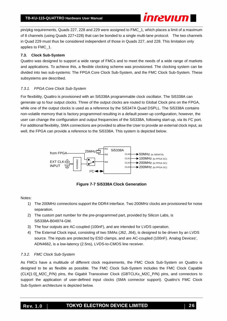
7.3. Clock Sub-System Quattro was designed to support a wide range of FMCs and to meet the needs of a wide range of markets and applications. To achieve this, a flexible clocking scheme was provisioned. The clocking system can be divided into two sub-systems: The FPGA Core Clock Sub-System, and the FMC Clock Sub-System. These subsystems are described.
7.3.1. FPGA Core Clock Sub-System
For flexibility, Quattro is provisioned with an Si5338A programmable clock oscillator. The Si5338A can generate up to four output clocks. Three of the output clocks are routed to Global Clock pins on the FPGA, while one of the output clocks is used as a reference by the Si5347A Quad DSPLL. The Si5338A contains non-volatile memory that is factory programmed resulting in a default power-up configuration, however, the user can change the configuration and output frequencies of the Si5338A, following start-up, via its I2C port. For additional flexibility, SMA connections are provided to allow the User to provide an external clock input, as well, the FPGA can provide a reference to the Si5338A. This system is depicted below.
Si5338A50MHz (to Si5347A)
100MHz (to FPGA GC)
200MHz (to FPGA GC)
200MHz (to FPGA GC)
I2C
25MHz
ADN
4662EXT CLK
INPUT
from FPGA CLK0
CLK1
CLK2
CLK3
IN1
IN2
IN3
Figure 7-7 Si5338A Clock Generation
Notes: 1) The 200MHz connections support the DDR4 interface. Two 200MHz clocks are provisioned for noise
separation. 2) The custom part number for the pre-programmed part, provided by Silicon Labs, is
Si5338A-B04974-GM. 3) The four outputs are AC-coupled (100nF), and are intended for LVDS operation. 4) The External Clock input, consisting of two SMAs (J62, J64), is designed to be driven by an LVDS
source. The inputs are protected by ESD clamps, and are AC-coupled (100nF). Analog Devices’, ADN4662, is a low-latency (2.5ns), LVDS-to-CMOS line receiver.
7.3.2. FMC Clock Sub-System
As FMCs have a multitude of different clock requirements, the FMC Clock Sub-System on Quattro is designed to be as flexible as possible. The FMC Clock Sub-System includes the FMC Clock Capable (CLK[1:0]_M2C_P/N) pins, the Gigabit Transceiver Clock (GBTCLKx_M2C_P/N) pins, and connectors to support the application of user-defined input clocks (SMA connector support). Quattro’s FMC Clock Sub-System architecture is depicted below.

TB-KU-115-QUATTRO Hardware User Manual
27 Rev. 1.0
FMC 0
FMC 1
FMC 2
FMC 3
QUAD224
QUAD225
QUAD226
QUAD227
QUAD228
QUAD229 (085,115 only)
GTH_CLK_M2C_0GTH_CLK_M2C_1
QUAD126
QUAD127
QUAD128
GTH_CLK_M2C_1GTH_CLK_M2C_0
QUAD230 (085,115 only)
QUAD231 (085,115 only)
QUAD232 (085,115 only)
4 GTH Channels
4 GTH Channels
2 GTH Channels
4 GTH Channels
4 GTH Channels
2 GTH Channels (085,115 only)
4 GTH Channels
4 GTH Channels
2 GTH Channels
4 GTH Channels (085,115 only)
4 GTH Channels (085,115 only)
2 GTH Channels (085,115 only)
GTH_CLK_M2C_0GTH_CLK_M2C_1
GTH_CLK_M2C_0GTH_CLK_M2C_1
REFCLK0
REFCLK1
REFCLK0
REFCLK1
REFCLK0
REFCLK1
REFCLK0
REFCLK1
REFCLK0 REFCLK1
REFCLK0 REFCLK1
REFCLK0 REFCLK1
REFCLK0 REFCLK1
CLK_SMA_QUAD227
CLK_SMA_QUAD126
CLK_SMA_QUAD230
GENERAL PURPOSECLOCKING RESOURCES
SI5338 CLOCKGENERATOR
25M XTAL
QUADPLL
50M_REF_CLK
FMC0_REC_CLK CLK_PLL_FMC0_GTH_REF
CLK_GLBL_FPGA (100M)
CLK_DDR4_1_200M
EXT_REF_CLK
SMACONNECTORS
CLK_SMA_QUAD224
CLK_SMA_QUAD227
CLK_SMA_QUAD126
CLK_SMA_QUAD230
REFCLK0
1:2BUFFER
2:1MUX
EXT_SYNC_OUT
EXT_SYNC_IN
Kintex Ultrascale
REFCLK1
EXT_CLK_OUTEXT_CLK_IN
EXT_SYNC_OUT
EXT_SYNC_IN
refref
refref
REFCLK0
REFCLK1
REFCLK0
REFCLK1
REFCLK0
REFCLK1
CLK_PLL_FMC1A_GTH_REF
CLK_PLL_FMC1B_GTH_REF
CLK_PLL_FMC2_GTH_REF
CLK_PLL_FMC3_GTH_REF
FMC1_REC_CLK
FMC2_REC_CLKFMC3_REC_CLK
FMC0_REC_CLK
FMC1_REC_CLK
FMC2_REC_CLK
FMC3_REC_CLK
CLK_PLL_FMC0_GTH_REF
CLK_PLL_FMC1A_GTH_REF
CLK_PLL_FMC1B_GTH_REF
CLK_PLL_FMC2_GTH_REF
CLK_PLL_FMC3_GTH_REF
CLK_MGTREFCLK1
CLK_MGTREFCLK0
CLK_MGTREFCLK1
CLK_MGTREFCLK0156.25MHz OSC
CLK_SMA_QUAD224
CLK_DDR4_2_200M
CLK_FMC_0_CLK0_M2CCLK_FMC_0_CLK1_M2C
CLK_FMC_1_CLK0_M2CCLK_FMC_1_CLK1_M2C
CLK_FMC_2_CLK0_M2CCLK_FMC_2_CLK1_M2C
CLK_FMC_0_CLK0_M2CCLK_FMC_0_CLK1_M2C
Figure 7-8 FMC Clock Sub-System Architecture
FMC Clock Capable Pins As depicted above, the FMC Clock Capable pins (CLK[1:0]_M2C_P/N) are connected to the Global Clock pins on the FPGA, in the respective bank. The CLK[3:2]_BIDIR_P/N pins on the FMC are left unconnected. Gigabit Transceiver Clocks Each FMC port provides two LVDS GBT Clock outputs (GBTCLK[1:0]_M2C_P/N). Both GBT Clock outputs are routed to the corresponding MGTREFCLK port on the FPGA. Typically, these are connected to the middle bank transceiver locations in order to take advantage of the North-South MGTREFCLK routing within the UltraScale FPGA. Additionally, an Si5347A, Quad DSPLL® Jitter Attenuator, is provisioned. The implementation is shown below:

TB-KU-115-QUATTRO Hardware User Manual
28 Rev. 1.0
Si5347Ato MGTREFCLK for FMC0 bank OUT0
OUT1SPAREPLL CLK OUTPUTSMAsto MGTREFCLK for FMC1A bank OUT2
to MGTREFCLK for General, SFP+, or FMC3 bank useOUT3to MGTREFCLK for FMC2 bank OUT4
to Test Points OUT5to MGTREFCLK for FMC1B bank OUT6
LOL[D:A] Loss of Lock status to I2C I/O Expander
FMC0 Recovered Clock
FMC1 Recovered ClockFMC2 Recovered Clock
FMC3 Recovered Clock
I2C
Reference Clock
IN0IN1IN2
IN3
XA/XB
from FPGA
from Si5338A
Figure 7-9 Si5437A, Gigabit Transceiver System The Si5347A feature set includes:
• Clock Generation. Any input frequency to any output frequency. • Jitter removal/attenuation. Including programmable bandwidth jitter filters. • Crosspoints. Any input to any output configuration.
A typical application would see the user receiving or recovering a clock from the FMC interface, outputting the ‘noisy’ received clock to the Si5347A, have the Si5347A ‘clean’ the clock, and then provide the clock back to the MGT port for use in re-transmission or synchronized transmission applications. PLL filtering was provisioned to enable transmission, or re-transmission, with minimal phase-noise.
SMA Clock/Synchronization Input/Output Support
Several SMA connectors are provisioned on Quattro to enable the receiving or transmission of clock or synchronization signals. These are depicted below.
MGTREFCLK230
FPGA
PROGCLOCK
GENERATORSi5338
QUAD PLL(jitter filter)
Si5347
EXT CLKinEXT CLKout
EXT SYNCinEXT SYNCout
MGTREFCLK227MGTREFCLK126
MGTREFCLK224
Si5347 REFout
AD
N46
62EXT REF input to Si5338
Figure 7-10 SMA Clock/Reference Architecture
As can be seen above, each MGT associated with an FMC port supports the application of an external MGTREFCLK. In addition, the FPGA can transmit and receive external clocks via SMAs. An important feature

TB-KU-115-QUATTRO Hardware User Manual
29 Rev. 1.0
of Quattro is the capability of synchronizing multiple Quattro (or other boards). This can be accomplished through external clock references, or through the provisioned Synchronization input and output.
The table below describes the provisioned SMAs.
Table 7-6 SMA Clock and Reference Ports SMA Name Dir. Type FPGA Connection Description J3 (P), J4 (N) MGTREFCLK224 Input LVDS B224_MGTREFCLK1 AC-coupled,100Ω J15 (P), J16 (N) MGTREFCLK227 Input LVDS B227_MGTREFCLK1 AC-coupled,100Ω J9 (P), J10 (N) MGTREFCLK126 Input LVDS B126_MGTREFCLK1 AC-coupled,100Ω J12 (P), J13 (N) MGTREFCLK230 Input LVDS B230_MGTREFCLK1 AC-coupled,100Ω J65 (P), J66 (N) Ext Sync Output Output LVDS GPIO, LVCMOS AC-coupled,100Ω J67 (P), J68 (N) Ext Sync Input Input LVDS GPIO(QBC), LVCMOS AC-coupled,100Ω J61 (P), J63 (N) Ext Clock Output Output LVDS GPIO(QBC), LVCMOS AC-coupled,100Ω J53 (P), J54 (N) Ext Clock Input Input LVDS Global Clock, LVDS AC-coupled,100Ω J77 (P), J76 (N) Si5347A Ref Out Output LVDS N/A DC-coupled,100Ω J62 (P), J64 (N) Si5338A Ref In Input LVDS N/A AC-coupled,100Ω

TB-KU-115-QUATTRO Hardware User Manual
30 Rev. 1.0
7.4. FMC Connector Interface Quattro has 4 high-pin count (HPC) 400 pin FMC connectors (FMC 0 to 3) on board. The following port provisioning was selected as good trade-off between functional support and FPGA resource availability.
Table 7-7 FMC Port I/O Support IO ASSIGNMENTS
GTH LA HA VADJ (V) FMC0 DP[9:0]_M2C
DP[9:0]_C2M LA[33:0] HA[4:0] 1.8,2.5,3.3
FMC1 DP[9:0]_M2C DP[9:0]_C2M3
LA[33:0] N/A 1.5, 1.8 (common VADJ) FMC2 DP[9:0]_M2C
DP[9:0]_C2M LA[18:0]
LA[23:19]4 N/A
FMC3 DP[9:0]_M2C DP[9:0]_C2M
LA[33:0] N/A
7.4.1. FMC Port Ordering
The FMC Ports are not in numerical order:
Figure 7-11 FMC Port Numbering
3 Due to SLR split, 10GTHs are available but only 8 can be grouped 4 Single ended support only
FMC3
FMC2
FMC0
FMC1
TB-KU-115-QUATTRO Hardware User Manual
31 Rev. 1.0
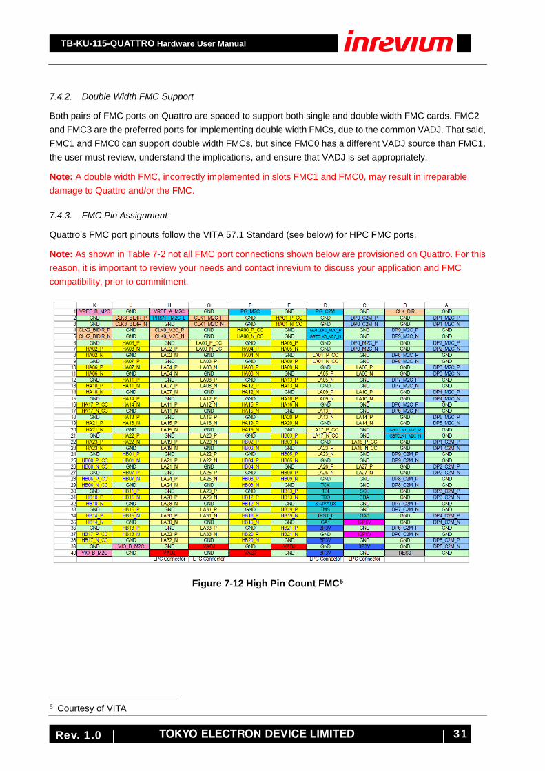
7.4.2. Double Width FMC Support
Both pairs of FMC ports on Quattro are spaced to support both single and double width FMC cards. FMC2 and FMC3 are the preferred ports for implementing double width FMCs, due to the common VADJ. That said, FMC1 and FMC0 can support double width FMCs, but since FMC0 has a different VADJ source than FMC1, the user must review, understand the implications, and ensure that VADJ is set appropriately.
Note: A double width FMC, incorrectly implemented in slots FMC1 and FMC0, may result in irreparable damage to Quattro and/or the FMC.
7.4.3. FMC Pin Assignment
Quattro’s FMC port pinouts follow the VITA 57.1 Standard (see below) for HPC FMC ports.
Note: As shown in Table 7-2 not all FMC port connections shown below are provisioned on Quattro. For this reason, it is important to review your needs and contact inrevium to discuss your application and FMC compatibility, prior to commitment.
Figure 7-12 High Pin Count FMC5
5 Courtesy of VITA

TB-KU-115-QUATTRO Hardware User Manual
32 Rev. 1.0
7.4.4. FMC Port Implementation Detail: Power, FMC SCL/SDA, GA0/GA1, TDI/TDO
The structure shown below is replicated for all FMC connectors on this board (with the exception of test points and reference designators being different per FMC). Note that VIO_B_M2C and VREF_[B:A]_M2C are only connected to Test Points, and not to the FPGA.
Figure 7-13 FMC_0 - 3 (SCL/SDA, GA0/GA1, TDI/TDO) As can be seen above, each power rail has a dedicated PTC for over-current protection. Note: While it is true that PTC’s offer some protection to overcurrent events, PTCs can be slow to react to long lasting, non-dramatic, over-current events, thus, care and attention should always be paid. Note: Following an over-current event, in which the PTC has activated, the user should remove all power from the board for a period of 5 minutes to allow the PTC to cool and “reset” itself. The following table describes the PTCs implemented on the FMC port rails.
Table 7-8 FMC Over-Current Protection PTCs FMC Rail Imax (A)6 MFR MPN Description 12V 1 Littelfuse 1812L150/12DR PTC RESETTABLE FUSE 12V, 1.5A 3V3 3 Littelfuse 1206L350SLTHYR PTC RESETTABLE FUSE 6V, 3.5A VADJ 4 Littelfuse 1206L350SLTHYR PTC RESETTABLE FUSE 6V, 3.5A7
For deeper understanding and to set expectations regarding the operation and expected results of the PTC-based protection, please review the datasheets for the devices described above.
6 As per VITA 57.1 7 Due to typical VADJ usage on FMCs, it was determined to be acceptable to limit VADJ with a 3.5A PTC. If this is an issue for your application, please discuss workarounds with inrevium.

TB-KU-115-QUATTRO Hardware User Manual
33 Rev. 1.0
7.4.5. FMC0 (J1) Pin Assignment
FMC0 connects all of the available LA signals and 6 HA differential pairs to banks on the FPGA.
High Speed: • 10 GTH channels connected
Low Speed:
• 34 differential LA pairs • 5 differential HA pairs • 2 differential clock pairs

TB-KU-115-QUATTRO Hardware User Manual
34 Rev. 1.0
Table 7-9 FMC0 (J1) to FPGA Pinout (Rows A-B) Bank# Pin# A B Pin# Bank#
-- GND 1 CLK_DIR #N/A #N/A
22 AV2 DP1_M2C_P 2 GND -- 22 AV1 DP1_M2C_N 3 GND --
-- GND 4 DP9_M2C_P AK2 22 -- GND 5 DP9_M2C_N AK1 22
22 AU4 DP2_M2C_P 6 GND -- 22 AU3 DP2_M2C_N 7 GND --
-- GND 8 DP8_M2C_P AL4 22 -- GND 9 DP8_M2C_N AL3 22
22 AT2 DP3_M2C_P 10 GND -- 22 AT1 DP3_M2C_N 11 GND --
-- GND 12 DP7_M2C_P AM2 22 -- GND 13 DP7_M2C_N AM1 22
22 AR4 DP4_M2C_P 14 GND -- 22 AR3 DP4_M2C_N 15 GND --
-- GND 16 DP6_M2C_P AN4 22 -- GND 17 DP6_M2C_N AN3 22
22 AP2 DP5_M2C_P 18 GND -- 22 AP1 DP5_M2C_N 19 GND --
-- GND 20 *1 GBTCLK1_M2C_P #N/A #N/A -- GND 21 *1
#N/A #N/A 22 AV6 DP1_C2M_P 22 GND -- 22 AV5 DP1_C2M_N 23 GND --
-- GND 24 DP9_C2M_P AK6 22 -- GND 25 DP9_C2M_N AK5 22
22 AU8 DP2_C2M_P 26 GND -- 22 AU7 DP2_C2M_N 27 GND --
-- GND 28 DP8_C2M_P AL8 22 -- GND 29 DP8_C2M_N AL7 22
22 AT6 DP3_C2M_P 30 GND -- 22 AT5 DP3_C2M_N 31 GND --
-- GND 32 DP7_C2M_P AM6 22 -- GND 33 DP7_C2M_N AM5 22
22 AR8 DP4_C2M_P 34 GND -- 22 AR7 DP4_C2M_N 35 GND --
-- GND 36 DP6_C2M_P AN8 22 -- GND 37 DP6_C2M_N AN7 22
22 AP6 DP5_C2M_P 38 GND -- 22 AP5 DP5_C2M_N 39 GND --
-- GND 40 RES0 --
TB-KU-115-QUATTRO Hardware User Manual
35 Rev. 1.0
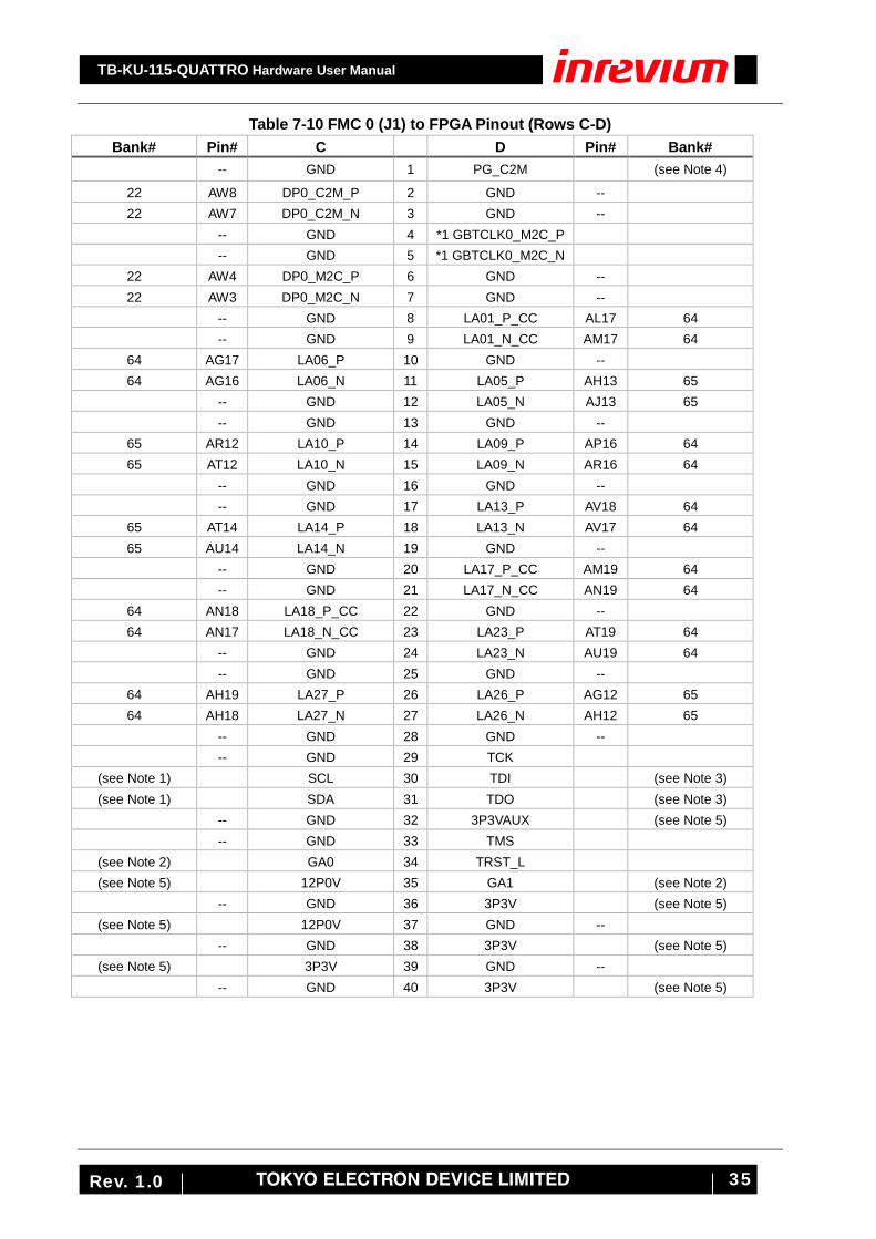
Table 7-10 FMC 0 (J1) to FPGA Pinout (Rows C-D) Bank# Pin# C D Pin# Bank#
-- GND 1 PG_C2M (see Note 4)
22 AW8 DP0_C2M_P 2 GND -- 22 AW7 DP0_C2M_N 3 GND -- -- GND 4 *1 GBTCLK0_M2C_P -- GND 5 *1 GBTCLK0_M2C_N
22 AW4 DP0_M2C_P 6 GND -- 22 AW3 DP0_M2C_N 7 GND -- -- GND 8 LA01_P_CC AL17 64 -- GND 9 LA01_N_CC AM17 64
64 AG17 LA06_P 10 GND -- 64 AG16 LA06_N 11 LA05_P AH13 65 -- GND 12 LA05_N AJ13 65 -- GND 13 GND --
65 AR12 LA10_P 14 LA09_P AP16 64 65 AT12 LA10_N 15 LA09_N AR16 64 -- GND 16 GND -- -- GND 17 LA13_P AV18 64
65 AT14 LA14_P 18 LA13_N AV17 64 65 AU14 LA14_N 19 GND -- -- GND 20 LA17_P_CC AM19 64 -- GND 21 LA17_N_CC AN19 64
64 AN18 LA18_P_CC 22 GND -- 64 AN17 LA18_N_CC 23 LA23_P AT19 64 -- GND 24 LA23_N AU19 64 -- GND 25 GND --
64 AH19 LA27_P 26 LA26_P AG12 65 64 AH18 LA27_N 27 LA26_N AH12 65 -- GND 28 GND -- -- GND 29 TCK
(see Note 1) SCL 30 TDI (see Note 3) (see Note 1) SDA 31 TDO (see Note 3)
-- GND 32 3P3VAUX (see Note 5) -- GND 33 TMS
(see Note 2) GA0 34 TRST_L (see Note 5) 12P0V 35 GA1 (see Note 2)
-- GND 36 3P3V (see Note 5) (see Note 5) 12P0V 37 GND --
-- GND 38 3P3V (see Note 5) (see Note 5) 3P3V 39 GND --
-- GND 40 3P3V (see Note 5)

TB-KU-115-QUATTRO Hardware User Manual
36 Rev. 1.0
Table 7-11 FMC 0 (J1) to FPGA Pinout (Rows E-F) Bank# Pin# E F Pin# Bank#
-- GND 1 PG_M2C (see Note 4)
65 AN13 HA01_P_CC 2 GND -- 65 AN12 HA01_N_CC 3 GND -- -- GND 4 HA00_P_CC AL14 65 -- GND 5 HA00_N_CC AL13 65 -- HA05_P 6 GND -- -- HA05_N 7 HA04_P AV13 65 -- GND 8 HA04_N AW13 65 -- HA09_P 9 GND -- -- HA09_N 10 HA08_P -- -- GND 11 HA08_N -- -- HA13_P 12 GND -- -- HA13_N 13 HA12_P -- -- GND 14 HA12_N -- -- HA16_P 15 GND -- -- HA16_N 16 HA15_P -- -- GND 17 HA15_N -- -- HA20_P 18 GND -- -- HA20_N 19 HA19_P -- -- GND 20 HA19_N -- -- HB03_P 21 GND -- -- HB03_N 22 HB02_P -- -- GND 23 HB02_N -- -- HB05_P 24 GND -- -- HB05_N 25 HB04_P -- -- GND 26 HB04_N -- -- HB09_P 27 GND -- -- HB09_N 28 HB08_P -- -- GND 29 HB08_N -- -- HB13_P 30 GND -- -- HB13_N 31 HB12_P -- -- GND 32 HB12_N -- -- HB19_P 33 GND -- -- HB19_N 34 HB16_P -- -- GND 35 HB16_N -- -- HB21_P 36 GND -- -- HB21_N 37 HB20_P -- -- GND 38 HB20_N --
(see Note 5) VADJ 39 GND -- -- GND 40 VADJ (see Note 5)

TB-KU-115-QUATTRO Hardware User Manual
37 Rev. 1.0
Table 7-12 FMC 0 (J1) to FPGA Pinout (Rows G-H) Bank# Pin# G H Pin# Bank#
-- GND 1 VREF_A_M2C (see Note 6)
65 AL12 CLK1_M2C_P 2 PRSNT_M2C_L (see Note 4) 65 AM12 CLK1_M2C_N 3 GND -- -- GND 4 CLK0_M2C_P AM14 65 -- GND 5 CLK0_M2C_N AN14 65
64 AL19 LA00_P_CC 6 GND -- 64 AL18 LA00_N_CC 7 LA02_P AE17 64 -- GND 8 LA02_N AF17 64
65 AP15 LA03_P 9 GND -- 65 AR15 LA03_N 10 LA04_P AD16 64 -- GND 11 LA04_N AE16 64
65 AE12 LA08_P 12 GND -- 65 AF12 LA08_N 13 LA07_P AD14 65 -- GND 14 LA07_N AD13 65
64 AT18 LA12_P 15 GND -- 64 AT17 LA12_N 16 LA11_P AE18 64 -- GND 17 LA11_N AF18 64
64 AJ16 LA16_P 18 GND -- 64 AK16 LA16_N 19 LA15_P AK18 64 -- GND 20 LA15_N AK17 64
64 AP19 LA20_P 21 GND -- 64 AP18 LA20_N 22 LA19_P AW20 64 -- GND 23 LA19_N AW19 64
64 AR20 LA22_P 24 GND -- 64 AT20 LA22_N 25 LA21_P AH17 64 -- GND 26 LA21_N AH16 64
65 AF15 LA25_P 27 GND -- 65 AG15 LA25_N 28 LA24_P AK13 65 -- GND 29 LA24_N AK12 65
65 AH14 LA29_P 30 GND -- 65 AJ14 LA29_N 31 LA28_P AJ15 65 -- GND 32 LA28_N AK15 65
64 AJ19 LA31_P 33 GND -- 64 AJ18 LA31_N 34 LA30_P AU17 64 -- GND 35 LA30_N AU16 64
64 AR18 LA33_P 36 GND -- 64 AR17 LA33_N 37 LA32_P AV19 64 -- GND 38 LA32_N AW18 64
(see Note 5) VADJ 39 GND -- -- GND 40 VADJ (see Note 5)

TB-KU-115-QUATTRO Hardware User Manual
38 Rev. 1.0
Table 7-13 FMC 0 (J1) to FPGA Pinout (Rows J-K) Bank# Pin# J K Pin# Bank#
-- GND 1 VREF_B_M2C (see Note 6)
-- CLK3_M2C_P 2 GND -- -- CLK3_M2C_N 3 GND -- -- GND 4 CLK2_M2C_P -- -- GND 5 CLK2_M2C_N --
65 AT15 HA03_P 6 GND -- 65 AU15 HA03_N 7 HA02_P AU12 65
-- GND 8 HA02_N AV12 65 -- HA07_P 9 GND -- -- HA07_N 10 HA06_P -- -- GND 11 HA06_N -- -- HA11_P 12 GND -- -- HA11_N 13 HA10_P -- -- GND 14 HA10_N -- -- HA14_P 15 GND -- -- HA14_N 16 HA17_P_CC -- -- GND 17 HA17_N_CC -- -- HA18_P 18 GND -- -- HA18_N 19 HA21_P -- -- GND 20 HA21_N -- -- HA22_P 21 GND -- -- HA22_N 22 HA23_P -- -- GND 23 HA23_N -- -- HB01_P 24 GND -- -- HB01_N 25 HB00_P_CC -- -- GND 26 HB00_N_CC -- -- HB07_P 27 GND -- -- HB07_N 28 HB06_P_CC -- -- GND 29 HB06_N_CC -- -- HB11_P 30 GND -- -- HB11_N 31 HB10_P -- -- GND 32 HB10_N -- -- HB15_P 33 GND -- -- HB15_N 34 HB14_P -- -- GND 35 HB14_N -- -- HB18_P 36 GND -- -- HB18_N 37 HB17_P_CC -- -- GND 38 HB17_N_CC --
(see Note 7) VIO_B_M2C 39 GND -- -- GND 40 VIO_B_M2C (see Note 7)
TB-KU-115-QUATTRO Hardware User Manual
39 Rev. 1.0
For FMC 0 (J1): Note 1: SCL, SDA
The board provides test points (CLK_FMC_I2C_OD/SDA_FMC_I2C_OD) with pull-up options to enable I2C communication with the system I2C network. (Default: pulled-up).
Note 2: GA0, GA1 This board provides pull-up or pull-down options for these connections. (Default: GA0 & GA1 = pulled-down)
Note 3: TDI, TDO The JTAG TDO pin is connected with a loopback to TDI through a 0 ohm resistor. (Default: floating).
Note 4: PG_C2M, PG_M2C, PRSNT_M2C_N These pins all have a resistor option for either pull-up or pull-down. (Default: PG_C2M = floating, PRSNT_M2C_N & PG_M2C = pulled-up)
Note 5: Power Rails This card provides a 12V output through the 12V0 pins and 3.3V output through the 3V3 and 3V3_AUX pins. It is important to note that all the FMC connectors present on this board are equipped with a fuse on the 12V0 rail. Lastly, the VADJ pins provide a 1.8V/2.5V/3.3V rail to FPGA mezzanine cards.
Note 6: VREF_A_M2C, VREF_B_M2C These terminals can be monitored by test points TP71 and TP72.
Note 7: VIO_B_M2C Both pins J39 and K40 for this terminal can also be monitored by test point TP69.

TB-KU-115-QUATTRO Hardware User Manual
40 Rev. 1.0
7.4.6. FMC1 (J2) Pin Assignment
This FMC connects GTH lanes and all of the available LA signals to banks on the FPGA.
High Speed: • 10 GTH channels connected
Low Speed:
• 34 differential LA pairs • 2 differential clock pairs

TB-KU-115-QUATTRO Hardware User Manual
41 Rev. 1.0
Table 7-14 FMC 1 (J2) to FPGA Pinout (Rows A-B) Bank# Pin# A B Pin# Bank#
-- GND 1 CLK_DIR
22 V2 DP1_M2C_P 2 GND -- 22 V1 DP1_M2C_N 3 GND --
-- GND 4 DP9_M2C_P R4 22 -- GND 5 DP9_M2C_N R3 22
22 Y2 DP2_M2C_P 6 GND -- 22 Y1 DP2_M2C_N 7 GND --
-- GND 8 DP8_M2C_P T2 22 -- GND 9 DP8_M2C_N T1 22
22 AB2 DP3_M2C_P 10 GND -- 22 AB1 DP3_M2C_N 11 GND --
-- GND 12 DP7_M2C_P AC4 22 -- GND 13 DP7_M2C_N AC3 22
22 AG4 DP4_M2C_P 14 GND -- 22 AG3 DP4_M2C_N 15 GND --
-- GND 16 DP6_M2C_P AD2 22 -- GND 17 DP6_M2C_N AD1 22
22 AF2 DP5_M2C_P 18 GND -- 22 AF1 DP5_M2C_N 19 GND --
-- GND 20 *1 GBTCLK1_M2C_P -- GND 21 *1
22 V6 DP1_C2M_P 22 GND -- 22 V5 DP1_C2M_N 23 GND --
-- GND 24 DP9_C2M_P T6 22 -- GND 25 DP9_C2M_N T5 22
22 AA4 DP2_C2M_P 26 GND -- 22 AA3 DP2_C2M_N 27 GND --
-- GND 28 DP8_C2M_P U4 22 -- GND 29 DP8_C2M_N U3 22
22 AB6 DP3_C2M_P 30 GND -- 22 AB5 DP3_C2M_N 31 GND --
-- GND 32 DP7_C2M_P AD6 22 -- GND 33 DP7_C2M_N AD5 22
22 AG8 DP4_C2M_P 34 GND -- 22 AG7 DP4_C2M_N 35 GND --
-- GND 36 DP6_C2M_P AE4 22 -- GND 37 DP6_C2M_N AE3 22
22 AF6 DP5_C2M_P 38 GND -- 22 AF5 DP5_C2M_N 39 GND --
-- GND 40 RES0 --

TB-KU-115-QUATTRO Hardware User Manual
42 Rev. 1.0
Table 7-15 FMC 1 (J2) to FPGA Pinout (Rows C-D) Bank# Pin# C D Pin# Bank#
-- GND 1 PG_C2M (see Note 4)
22 Y6 DP0_C2M_P 2 GND -- 22 Y5 DP0_C2M_N 3 GND -- -- GND 4 *1 GBTCLK0_M2C_P -- GND 5 *1 GBTCLK0_M2C_N
22 W4 DP0_M2C_P 6 GND -- 22 W3 DP0_M2C_N 7 GND -- -- GND 8 LA01_P_CC AM22 44 -- GND 9 LA01_N_CC AN22 44
44 AE22 LA06_P 10 GND -- 44 AF22 LA06_N 11 LA05_P AF20 44 -- GND 12 LA05_N AG20 44 -- GND 13 GND --
44 AR22 LA10_P 14 LA09_P AP21 44 44 AR23 LA10_N 15 LA09_N AR21 44 -- GND 16 GND -- -- GND 17 LA13_P AV21 44
44 AT23 LA14_P 18 LA13_N AW21 44 44 AT24 LA14_N 19 GND -- -- GND 20 LA17_P_CC AL27 45 -- GND 21 LA17_N_CC AL28 45
45 AK27 LA18_P_CC 22 GND -- 45 AK28 LA18_N_CC 23 LA23_P AE27 45 -- GND 24 LA23_N AF27 45 -- GND 25 GND --
45 AD25 LA27_P 26 LA26_P AD26 45 45 AE25 LA27_N 27 LA26_N AE26 45 -- GND 28 GND -- -- GND 29 TCK --
(see Note 1) SCL 30 TDI (see Note 3) (see Note 1) SDA 31 TDO (see Note 3)
-- GND 32 3P3VAUX (see Note 5) -- GND 33 TMS --
(see Note 2) GA0 34 TRST_L -- (see Note 5) 2P0V 35 GA1 (see Note 2)
-- GND 36 3P3V (see Note 5) (see Note 5) 12P0V 37 GND --
-- GND 38 3P3V (see Note 5) (see Note 5) 3P3V 39 GND --
-- GND 40 3P3V (see Note 5)
TB-KU-115-QUATTRO Hardware User Manual
43 Rev. 1.0
Table 7-16 FMC 1 (J2) to FPGA Pinout (Rows E-F) Bank# Pin# E F Pin# Bank#
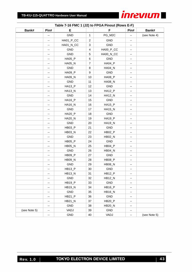
-- GND 1 PG_M2C -- (see Note 4)
-- HA01_P_CC 2 GND -- -- HA01_N_CC 3 GND -- -- GND 4 HA00_P_CC -- -- GND 5 HA00_N_CC -- -- HA05_P 6 GND -- -- HA05_N 7 HA04_P -- -- GND 8 HA04_N -- -- HA09_P 9 GND -- -- HA09_N 10 HA08_P -- -- GND 11 HA08_N -- -- HA13_P 12 GND -- -- HA13_N 13 HA12_P -- -- GND 14 HA12_N -- -- HA16_P 15 GND -- -- HA16_N 16 HA15_P -- -- GND 17 HA15_N -- -- HA20_P 18 GND -- -- HA20_N 19 HA19_P -- -- GND 20 HA19_N -- -- HB03_P 21 GND -- -- HB03_N 22 HB02_P -- -- GND 23 HB02_N -- -- HB05_P 24 GND -- -- HB05_N 25 HB04_P -- -- GND 26 HB04_N -- -- HB09_P 27 GND -- -- HB09_N 28 HB08_P -- -- GND 29 HB08_N -- -- HB13_P 30 GND -- -- HB13_N 31 HB12_P -- -- GND 32 HB12_N -- -- HB19_P 33 GND -- -- HB19_N 34 HB16_P -- -- GND 35 HB16_N -- -- HB21_P 36 GND -- -- HB21_N 37 HB20_P -- -- GND 38 HB20_N --
(see Note 5) -- VADJ 39 GND -- -- GND 40 VADJ -- (see Note 5)

TB-KU-115-QUATTRO Hardware User Manual
44 Rev. 1.0
Table 7-17 FMC 1 (J2) to FPGA Pinout (Rows G-H) Bank# Pin# G H Pin# Bank#
-- GND 1 VREF_A_M2C (see Note 6)
44 AK22 CLK1_M2C_P 2 PRSNT_M2C_L (see Note 4) 44 AL22 CLK1_M2C_N 3 GND -- -- GND 4 CLK0_M2C_P AK23 44 -- GND 5 CLK0_M2C_N AL23 44
44 AM21 LA00_P_CC 6 GND -- 44 AN21 LA00_N_CC 7 LA02_P AE23 44 -- GND 8 LA02_N AF23 44
44 AE20 LA03_P 9 GND -- 44 AE21 LA03_N 10 LA04_P AD20 44 -- GND 11 LA04_N AD21 44
44 AG21 LA08_P 12 GND -- 44 AG22 LA08_N 13 LA07_P AH22 44 -- GND 14 LA07_N AH23 44
44 AT22 LA12_P 15 GND -- 44 AU22 LA12_N 16 LA11_P AU21 44 -- GND 17 LA11_N AV22 44
44 AV23 LA16_P 18 GND -- 44 AW23 LA16_N 19 LA15_P AV24 44 -- GND 20 LA15_N AW24 44
45 AN28 LA20_P 21 GND -- 45 AP28 LA20_N 22 LA19_P AK20 44 -- GND 23 LA19_N AK21 44
44 AN23 LA22_P 24 GND -- 44 AP23 LA22_N 25 LA21_P AL20 44 -- GND 26 LA21_N AM20 44
45 AF25 LA25_P 27 GND -- 45 AG25 LA25_N 28 LA24_P AF24 45 -- GND 29 LA24_N AG24 45
45 AG26 LA29_P 30 GND -- 45 AG27 LA29_N 31 LA28_P AH24 45 -- GND 32 LA28_N AJ24 45
45 AL24 LA31_P 33 GND -- 45 AL25 LA31_N 34 LA30_P AH26 45 -- GND 35 LA30_N AJ26 45
44 AN24 LA33_P 36 GND -- 44 AP24 LA33_N 37 LA32_P AJ25 45 -- GND 38 LA32_N AK25 45
(see Note 5) VADJ 39 GND -- -- GND 40 VADJ (see Note 5)

TB-KU-115-QUATTRO Hardware User Manual
45 Rev. 1.0
Table 7-18 FMC 1 (J2) to FPGA Pinout (Rows J-K) Bank# Pin# J K Pin# Bank#
-- GND 1 VREF_B_M2C (see Note 6)
-- CLK3_M2C_P 2 GND -- -- CLK3_M2C_N 3 GND -- -- GND 4 CLK2_M2C_P -- -- GND 5 CLK2_M2C_N -- -- HA03_P 6 GND -- -- HA03_N 7 HA02_P -- -- GND 8 HA02_N -- -- HA07_P 9 GND -- -- HA07_N 10 HA06_P -- -- GND 11 HA06_N -- -- HA11_P 12 GND -- -- HA11_N 13 HA10_P -- -- GND 14 HA10_N -- -- HA14_P 15 GND -- -- HA14_N 16 HA17_P_CC -- -- GND 17 HA17_N_CC -- -- HA18_P 18 GND -- -- HA18_N 19 HA21_P -- -- GND 20 HA21_N -- -- HA22_P 21 GND -- -- HA22_N 22 HA23_P -- -- GND 23 HA23_N -- -- HB01_P 24 GND -- -- HB01_N 25 HB00_P_CC -- -- GND 26 HB00_N_CC -- -- HB07_P 27 GND -- -- HB07_N 28 HB06_P_CC -- -- GND 29 HB06_N_CC -- -- HB11_P 30 GND -- -- HB11_N 31 HB10_P -- -- GND 32 HB10_N -- -- HB15_P 33 GND -- -- HB15_N 34 HB14_P -- -- GND 35 HB14_N -- -- HB18_P 36 GND -- -- HB18_N 37 HB17_P_CC -- -- GND 38 HB17_N_CC --
(see Note 7) VIO_B_M2C 39 GND -- -- GND 40 VIO_B_M2C (see Note 7)

TB-KU-115-QUATTRO Hardware User Manual
46 Rev. 1.0
Notes for FMC 1 (J2): Note 1: SCL, SDA
The board provides test points (CLK_FMC_I2C_OD/SDA_FMC_I2C_OD) with pull-up options to enable I2C communication with the system I2C network. (Default: pulled-up).
Note 2: GA0, GA1 This board provides pull-up or pull-down options for these connections. (Default: GA0=pulled-down, GA1=pulled-up)
Note 3: TDI, TDO The JTAG TDO pin is connected with a loopback to TDI through a 0 ohm resistor. (Default: floating).
Note 4: PG_C2M, PG_M2C, PRSNT_M2C_N These pins all have a resistor option for either pull-up or pull-down. (Default: PG_C2M floating, PRSNT_M2C_N & PG_M2C pulled-up)
Note 5: Power Rails This card provides a 12V output through the 12V0 pins and 3.3V output through the 3V3 and 3V3_AUX pins. It is important to note that all the FMC connectors present on this board are equipped with a fuse on the 12V0 rail. Lastly, the VADJ pins provide a 1.8V/2.5V/3.3V rail to FPGA mezzanine cards.
Note 6: VREF_A_M2C, VREF_B_M2C These terminals can be monitored by test points TP75 and TP76.
Note 7: VIO_B_M2C Both pins J39 and K40 for this terminal can also be monitored by test point TP73.

TB-KU-115-QUATTRO Hardware User Manual
47 Rev. 1.0
7.4.7. FMC2 (J5) Pin Assignment
This FMC connects 10 GTH lanes and a mix of differential pairs and LVCMOS nets of LA signals to banks on the FPGA.
High Speed: • 10 GTH channels connected
Low Speed:
• 19 differential LA pairs • 10 LVCMOS LA nets • 2 differential clock pairs

TB-KU-115-QUATTRO Hardware User Manual
48 Rev. 1.0
Table 7-19 FMC 2 (J5) to FPGA Pinout (Rows A-B) Bank# Pin# A B Pin# Bank#
-- GND 1 CLK_DIR
12 AF36 DP1_M2C_P 2 GND -- 12 AF37 DP1_M2C_N 3 GND --
-- GND 4 DP9_M2C_P R38 12 -- GND 5 DP9_M2C_N R39 12
12 AE38 DP2_M2C_P 6 GND -- 12 AE39 DP2_M2C_N 7 GND --
-- GND 8 DP8_M2C_P U38 12 -- GND 9 DP8_M2C_N U39 12
12 AC38 DP3_M2C_P 10 GND -- 12 AC39 DP3_M2C_N 11 GND --
-- GND 12 DP7_M2C_P V36 12 -- GND 13 DP7_M2C_N V37 12
12 AB36 DP4_M2C_P 14 GND -- 12 AB37 DP4_M2C_N 15 GND --
-- GND 16 DP6_M2C_P W38 12 -- GND 17 DP6_M2C_N W39 12
12 AA38 DP5_M2C_P 18 GND -- 12 AA39 DP5_M2C_N 19 GND --
-- GND 20 *1 GBTCLK1_M2C_P -- GND 21 *1
12 AG3
DP1_C2M_P 22 GND -- 12 AG3
DP1_C2M_N 23 GND -- -- GND 24 DP9_C2M_P T36 12 -- GND 25 DP9_C2M_N T37 12
12 AE34 DP2_C2M_P 26 GND -- 12 AE35 DP2_C2M_N 27 GND --
-- GND 28 DP8_C2M_P U34 12 -- GND 29 DP8_C2M_N U35 12
12 AD36 DP3_C2M_P 30 GND -- 12 AD37 DP3_C2M_N 31 GND --
-- GND 32 DP7_C2M_P W34 12 -- GND 33 DP7_C2M_N W35 12
12 AC34 DP4_C2M_P 34 GND -- 12 AC35 DP4_C2M_N 35 GND --
-- GND 36 DP6_C2M_P Y36 12 -- GND 37 DP6_C2M_N Y37 12
12 AA34 DP5_C2M_P 38 GND -- 12 AA35 DP5_C2M_N 39 GND --
-- GND 40 RES0 --

TB-KU-115-QUATTRO Hardware User Manual
49 Rev. 1.0
Table 7-20 FMC 2 (J5) to FPGA Pinout (Rows C-D) Bank# Pin# C D Pin# Bank#
-- GND 1 PG_C2M (see Note 4)
12 AH36 DP0_C2M_P 2 GND -- 12 AH37 DP0_C2M_N 3 GND -- -- GND 4 *1 GBTCLK0_M2C_P -- GND 5 *1 GBTCLK0_M2C_N
12 AG38 DP0_M2C_P 6 GND -- 12 AG39 DP0_M2C_N 7 GND -- -- GND 8 LA01_P_CC AM27 45 -- GND 9 LA01_N_CC AN27 45
45 AU25 LA06_P 10 GND -- 45 AU26 LA06_N 11 LA05_P AR28 45 -- GND 12 LA05_N AT28 45 -- GND 13 GND --
24 AH28 LA10_P 14 LA09_P AV28 45 24 AJ28 LA10_N 15 LA09_N AW28 45 -- GND 16 GND -- -- GND 17 LA13_P AJ33 24
24 AH31 LA14_P 18 LA13_N AK33 24 24 AH32 LA14_N 19 GND -- -- GND 20 LA17_P_CC AH29 24 -- GND 21 LA17_N_CC AJ29 24
24 AK32 LA18_P_CC 22 GND -- 24 AL32 LA18_N_CC 23 LA23_P AG30 24 -- GND 24 LA23_N AL33 24 -- GND 25 GND -- -- LA27_P 26 LA26_P -- -- LA27_N 27 LA26_N -- -- GND 28 GND -- -- GND 29 TCK --
(see Note 1) SCL 30 TDI (see Note 3) (see Note 1) SDA 31 TDO (see Note 3)
-- GND 32 3P3VAUX (see Note 5) -- GND 33 TMS --
(see Note 2) GA0 34 TRST_L -- (see Note 5) 12P0V 35 GA1 (see Note 2)
-- GND 36 3P3V (see Note 5) (see Note 5) 12P0V 37 GND --
-- GND 38 3P3V (see Note 5) (see Note 5) 3P3V 39 GND --
-- GND 40 3P3V (see Note 5)

TB-KU-115-QUATTRO Hardware User Manual
50 Rev. 1.0
Table 7-21 FMC 2 (J5) to FPGA Pinout (Rows E-F) Bank# Pin# E F Pin# Bank#
-- GND 1 PG_M2C -- (see Note 4)
-- HA01_P_CC 2 GND -- -- HA01_N_CC 3 GND -- -- GND 4 HA00_P_CC -- -- GND 5 HA00_N_CC -- -- HA05_P 6 GND -- -- HA05_N 7 HA04_P -- -- GND 8 HA04_N -- -- HA09_P 9 GND -- -- HA09_N 10 HA08_P -- -- GND 11 HA08_N -- -- HA13_P 12 GND -- -- HA13_N 13 HA12_P -- -- GND 14 HA12_N -- -- HA16_P 15 GND -- -- HA16_N 16 HA15_P -- -- GND 17 HA15_N -- -- HA20_P 18 GND -- -- HA20_N 19 HA19_P -- -- GND 20 HA19_N -- -- HB03_P 21 GND -- -- HB03_N 22 HB02_P -- -- GND 23 HB02_N -- -- HB05_P 24 GND -- -- HB05_N 25 HB04_P -- -- GND 26 HB04_N -- -- HB09_P 27 GND -- -- HB09_N 28 HB08_P -- -- GND 29 HB08_N -- -- HB13_P 30 GND -- -- HB13_N 31 HB12_P -- -- GND 32 HB12_N -- -- HB19_P 33 GND -- -- HB19_N 34 HB16_P -- -- GND 35 HB16_N -- -- HB21_P 36 GND -- -- HB21_N 37 HB20_P -- -- GND 38 HB20_N --
(see Note 5) -- VADJ 39 GND -- -- GND 40 VADJ -- (see Note 5)

TB-KU-115-QUATTRO Hardware User Manual
51 Rev. 1.0
Table 7-22 FMC 2 (J5) to FPGA Pinout (Rows G-H) Bank# Pin# G H Pin# Bank#
-- GND 1 VREF_A_M2C (see Note 6)
24 AL30 CLK1_M2C_P 2 PRSNT_M2C_L (see Note 4) 24 AM30 CLK1_M2C_N 3 GND -- -- GND 4 CLK0_M2C_P AM31 24 -- GND 5 CLK0_M2C_N AN31 24
45 AM26 LA00_P_CC 6 GND -- 45 AN26 LA00_N_CC 7 LA02_P AM24 45 -- GND 8 LA02_N AM25 45
45 AR26 LA03_P 9 GND -- 45 AR27 LA03_N 10 LA04_P AV26 45 -- GND 11 LA04_N AV27 45
45 AW25 LA08_P 12 GND -- 45 AW26 LA08_N 13 LA07_P AT27 45 -- GND 14 LA07_N AU27 45
24 AE28 LA12_P 15 GND -- 24 AF28 LA12_N 16 LA11_P AF29 24 -- GND 17 LA11_N AG29 24
24 AJ31 LA16_P 18 GND -- 24 AK31 LA16_N 19 LA15_P AE30 24 -- GND 20 LA15_N AF30 24
44 AP20 LA20_P 21 GND -- 44 AU24 LA20_N 22 LA19_P AH21 44 -- GND 23 LA19_N AJ23 44
45 AP26 LA22_P 24 GND -- 45 AT25 LA22_N 25 LA21_P AH27 45 -- GND 26 LA21_N AK26 45 -- LA25_P 27 GND -- -- LA25_N 28 LA24_P -- -- GND 29 LA24_N -- -- LA29_P 30 GND -- -- LA29_N 31 LA28_P -- -- GND 32 LA28_N -- -- LA31_P 33 GND -- -- LA31_N 34 LA30_P -- -- GND 35 LA30_N -- -- LA33_P 36 GND -- -- LA33_N 37 LA32_P -- -- GND 38 LA32_N --
(see Note 5) VADJ 39 GND -- -- GND 40 VADJ (see Note 5)

TB-KU-115-QUATTRO Hardware User Manual
52 Rev. 1.0
Table 7-23 FMC 2 (J5) to FPGA Pinout (Rows J-K) Bank# Pin# J K Pin# Bank#
-- GND 1 VREF_B_M2C (see Note 6)
-- CLK3_M2C_P 2 GND -- -- CLK3_M2C_N 3 GND -- -- GND 4 CLK2_M2C_P -- -- GND 5 CLK2_M2C_N -- -- HA03_P 6 GND -- -- HA03_N 7 HA02_P -- -- GND 8 HA02_N -- -- HA07_P 9 GND -- -- HA07_N 10 HA06_P -- -- GND 11 HA06_N -- -- HA11_P 12 GND -- -- HA11_N 13 HA10_P -- -- GND 14 HA10_N -- -- HA14_P 15 GND -- -- HA14_N 16 HA17_P_CC -- -- GND 17 HA17_N_CC -- -- HA18_P 18 GND -- -- HA18_N 19 HA21_P -- -- GND 20 HA21_N -- -- HA22_P 21 GND -- -- HA22_N 22 HA23_P -- -- GND 23 HA23_N -- -- HB01_P 24 GND -- -- HB01_N 25 HB00_P_CC -- -- GND 26 HB00_N_CC -- -- HB07_P 27 GND -- -- HB07_N 28 HB06_P_CC -- -- GND 29 HB06_N_CC -- -- HB11_P 30 GND -- -- HB11_N 31 HB10_P -- -- GND 32 HB10_N -- -- HB15_P 33 GND -- -- HB15_N 34 HB14_P -- -- GND 35 HB14_N -- -- HB18_P 36 GND -- -- HB18_N 37 HB17_P_CC -- -- GND 38 HB17_N_CC --
(see Note 7) VIO_B_M2C 39 GND -- -- GND 40 VIO_B_M2C (see Note 7)

TB-KU-115-QUATTRO Hardware User Manual
53 Rev. 1.0
Notes for FMC 2 (J5):
Note 1: SCL, SDA The board provides test points (CLK_FMC_I2C_OD/SDA_FMC_I2C_OD) with pull-up options to enable I2C communication with the system I2C network. (Default: pulled-up).
Note 2: GA0, GA1 This board provides pull-up or pull-down options for these connections. (Default: GA0=pulled-up, GA1=pulled-down)
Note 3: TDI, TDO The JTAG TDO pin is connected with a loopback to TDI through a 0 ohm resistor. (Default: floating).
Note 4: PG_C2M, PG_M2C, PRSNT_M2C_N These pins all have a resistor option for either pull-up or pull-down. (Default: PG_C2M floating, PRSNT_M2C_N & PG_M2C pulled-up)
Note 5: Power Rails This card provides a 12V output through the 12V0 pins and 3.3V output through the 3V3 and 3V3_AUX pins. It is important to note that all the FMC connectors present on this board are equipped with a fuse on the 12V0 rail. Lastly, the VADJ pins provide a 1.8V/2.5V/3.3V rail to FPGA mezzanine cards.
Note 6: VREF_A_M2C, VREF_B_M2C These terminals can be monitored by test points TP79 and TP80.
Note 7: VIO_B_M2C Both pins J39 and K40 for this terminal can also be monitored by test point TP77.

TB-KU-115-QUATTRO Hardware User Manual
54 Rev. 1.0
7.4.8. FMC3 (J8) Pin Assignment
This FMC connects GTH lanes and all of the available LA signals to banks on the FPGA.
High Speed: • 10 GTH channels connected
Low Speed:
• 34 differential LA pairs • 2 differential clock pairs

TB-KU-115-QUATTRO Hardware User Manual
55 Rev. 1.0
Table 7-24 FMC 3 (J8) to FPGA Pinout (Rows A-B) Bank# Pin# A B Pin# Bank#
-- GND 1 CLK_DIR
23 L4 DP1_M2C_P 2 GND -- 23 L3 DP1_M2C_N 3 GND --
-- GND 4 DP9_M2C_P C4 23 -- GND 5 DP9_M2C_N C3 23
23 K2 DP2_M2C_P 6 GND -- 23 K1 DP2_M2C_N 7 GND --
-- GND 8 DP8_M2C_P D2 23 -- GND 9 DP8_M2C_N D1 23
23 J4 DP3_M2C_P 10 GND -- 23 J3 DP3_M2C_N 11 GND --
-- GND 12 DP7_M2C_P E4 23 -- GND 13 DP7_M2C_N E3 23
23 H2 DP4_M2C_P 14 GND -- 23 H1 DP4_M2C_N 15 GND --
-- GND 16 DP6_M2C_P F2 23 -- GND 17 DP6_M2C_N F1 23
23 G4 DP5_M2C_P 18 GND -- 23 G3 DP5_M2C_N 19 GND --
-- GND 20 *1 GBTCLK1_M2C_P #N/A #N/A -- GND 21 *1
#N/A #N/A 23 L8 DP1_C2M_P 22 GND -- 23 L7 DP1_C2M_N 23 GND --
-- GND 24 DP9_C2M_P C8 23 -- GND 25 DP9_C2M_N C7 23
23 K6 DP2_C2M_P 26 GND -- 23 K5 DP2_C2M_N 27 GND --
-- GND 28 DP8_C2M_P D6 23 -- GND 29 DP8_C2M_N D5 23
23 J8 DP3_C2M_P 30 GND -- 23 J7 DP3_C2M_N 31 GND --
-- GND 32 DP7_C2M_P E8 23 -- GND 33 DP7_C2M_N E7 23
23 H6 DP4_C2M_P 34 GND -- 23 H5 DP4_C2M_N 35 GND --
-- GND 36 DP6_C2M_P F6 23 -- GND 37 DP6_C2M_N F5 23
23 G8 DP5_C2M_P 38 GND -- 23 G7 DP5_C2M_N 39 GND --
-- GND 40 RES0 --

TB-KU-115-QUATTRO Hardware User Manual
56 Rev. 1.0
Table 7-25 FMC 3 (J8) to FPGA Pinout (Rows C-D) Bank# Pin# C D Pin# Bank#
-- GND 1 PG_C2M (see Note 4)
23 M6 DP0_C2M_P 2 GND -- 23 M5 DP0_C2M_N 3 GND -- -- GND 4 *1 GBTCLK0_M2C_P -- GND 5 *1 GBTCLK0_M2C_N
23 M2 DP0_M2C_P 6 GND -- 23 M1 DP0_M2C_N 7 GND -- -- GND 8 LA01_P_CC AM32 24 -- GND 9 LA01_N_CC AN32 24
24 AU29 LA06_P 10 GND -- 24 AU30 LA06_N 11 LA05_P AU31 24 -- GND 12 LA05_N AV31 24 -- GND 13 GND --
25 AU36 LA10_P 14 LA09_P AP30 24 25 AV36 LA10_N 15 LA09_N AP31 24 -- GND 16 GND -- -- GND 17 LA13_P AL37 25
25 AT34 LA14_P 18 LA13_N AL38 25 25 AU34 LA14_N 19 GND -- -- GND 20 LA17_P_CC AN36 25 -- GND 21 LA17_N_CC AN37 25
25 AR37 LA18_P_CC 22 GND -- 25 AT37 LA18_N_CC 23 LA23_P AM36 25 -- GND 24 LA23_N AM37 25 -- GND 25 GND --
24 AJ30 LA27_P 26 LA26_P AK35 25 24 AK30 LA27_N 27 LA26_N AK36 25 -- GND 28 GND -- -- GND 29 TCK
(see Note 1) SCL 30 TDI (see Note 3) (see Note 1) SDA 31 TDO (see Note 3)
-- GND 32 3P3VAUX (see Note 5) -- GND 33 TMS
(see Note 2) GA0 34 TRST_L (see Note 5) 12P0V 35 GA1 (see Note 2)
-- GND 36 3P3V (see Note 5) (see Note 5) 12P0V 37 GND --
-- GND 38 3P3V (see Note 5) (see Note 5) 3P3V 39 GND --
-- GND 40 3P3V (see Note 5)

TB-KU-115-QUATTRO Hardware User Manual
57 Rev. 1.0
Table 7-26 FMC 3 (J8) to FPGA Pinout (Rows E-F) Bank# Pin# E F Pin# Bank#
-- GND 1 PG_M2C -- (see Note 4)
-- HA01_P_CC 2 GND -- -- HA01_N_CC 3 GND -- -- GND 4 HA00_P_CC -- -- GND 5 HA00_N_CC -- -- HA05_P 6 GND -- -- HA05_N 7 HA04_P -- -- GND 8 HA04_N -- -- HA09_P 9 GND -- -- HA09_N 10 HA08_P -- -- GND 11 HA08_N -- -- HA13_P 12 GND -- -- HA13_N 13 HA12_P -- -- GND 14 HA12_N -- -- HA16_P 15 GND -- -- HA16_N 16 HA15_P -- -- GND 17 HA15_N -- -- HA20_P 18 GND -- -- HA20_N 19 HA19_P -- -- GND 20 HA19_N -- -- HB03_P 21 GND -- -- HB03_N 22 HB02_P -- -- GND 23 HB02_N -- -- HB05_P 24 GND -- -- HB05_N 25 HB04_P -- -- GND 26 HB04_N -- -- HB09_P 27 GND -- -- HB09_N 28 HB08_P -- -- GND 29 HB08_N -- -- HB13_P 30 GND -- -- HB13_N 31 HB12_P -- -- GND 32 HB12_N -- -- HB19_P 33 GND -- -- HB19_N 34 HB16_P -- -- GND 35 HB16_N -- -- HB21_P 36 GND -- -- HB21_N 37 HB20_P -- -- GND 38 HB20_N --
(see Note 5) -- VADJ 39 GND -- -- GND 40 VADJ -- (see Note 5)
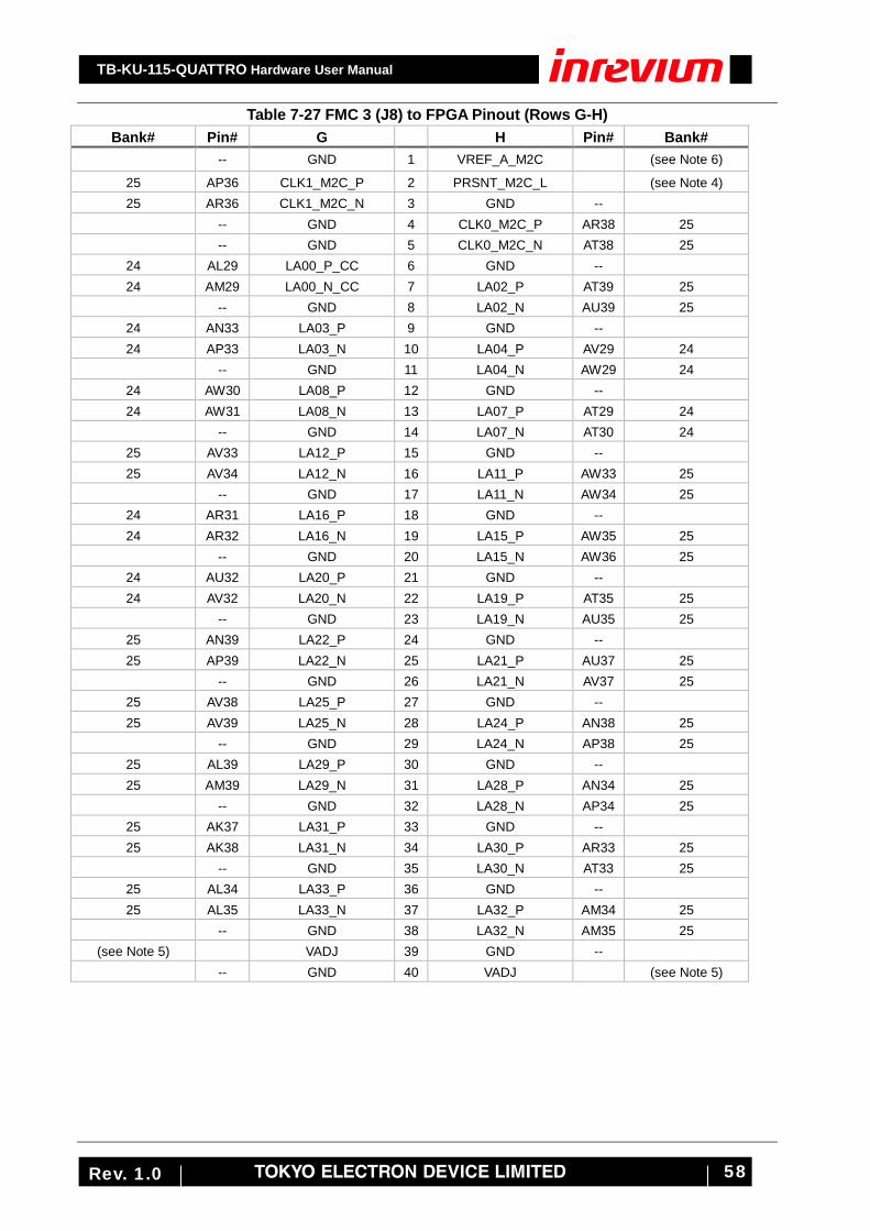
TB-KU-115-QUATTRO Hardware User Manual
58 Rev. 1.0
Table 7-27 FMC 3 (J8) to FPGA Pinout (Rows G-H) Bank# Pin# G H Pin# Bank#
-- GND 1 VREF_A_M2C (see Note 6)
25 AP36 CLK1_M2C_P 2 PRSNT_M2C_L (see Note 4) 25 AR36 CLK1_M2C_N 3 GND -- -- GND 4 CLK0_M2C_P AR38 25 -- GND 5 CLK0_M2C_N AT38 25
24 AL29 LA00_P_CC 6 GND -- 24 AM29 LA00_N_CC 7 LA02_P AT39 25 -- GND 8 LA02_N AU39 25
24 AN33 LA03_P 9 GND -- 24 AP33 LA03_N 10 LA04_P AV29 24 -- GND 11 LA04_N AW29 24
24 AW30 LA08_P 12 GND -- 24 AW31 LA08_N 13 LA07_P AT29 24 -- GND 14 LA07_N AT30 24
25 AV33 LA12_P 15 GND -- 25 AV34 LA12_N 16 LA11_P AW33 25 -- GND 17 LA11_N AW34 25
24 AR31 LA16_P 18 GND -- 24 AR32 LA16_N 19 LA15_P AW35 25 -- GND 20 LA15_N AW36 25
24 AU32 LA20_P 21 GND -- 24 AV32 LA20_N 22 LA19_P AT35 25 -- GND 23 LA19_N AU35 25
25 AN39 LA22_P 24 GND -- 25 AP39 LA22_N 25 LA21_P AU37 25 -- GND 26 LA21_N AV37 25
25 AV38 LA25_P 27 GND -- 25 AV39 LA25_N 28 LA24_P AN38 25 -- GND 29 LA24_N AP38 25
25 AL39 LA29_P 30 GND -- 25 AM39 LA29_N 31 LA28_P AN34 25 -- GND 32 LA28_N AP34 25
25 AK37 LA31_P 33 GND -- 25 AK38 LA31_N 34 LA30_P AR33 25 -- GND 35 LA30_N AT33 25
25 AL34 LA33_P 36 GND -- 25 AL35 LA33_N 37 LA32_P AM34 25 -- GND 38 LA32_N AM35 25
(see Note 5) VADJ 39 GND -- -- GND 40 VADJ (see Note 5)

TB-KU-115-QUATTRO Hardware User Manual
59 Rev. 1.0
Table 7-28 FMC 3 (J8) to FPGA Pinout (Rows J-K) Bank# Pin# J K Pin# Bank#
-- GND 1 VREF_B_M2C (see Note 6)
-- CLK3_M2C_P 2 GND -- -- CLK3_M2C_N 3 GND -- -- GND 4 CLK2_M2C_P -- -- GND 5 CLK2_M2C_N -- -- HA03_P 6 GND -- -- HA03_N 7 HA02_P -- -- GND 8 HA02_N -- -- HA07_P 9 GND -- -- HA07_N 10 HA06_P -- -- GND 11 HA06_N -- -- HA11_P 12 GND -- -- HA11_N 13 HA10_P -- -- GND 14 HA10_N -- -- HA14_P 15 GND -- -- HA14_N 16 HA17_P_CC -- -- GND 17 HA17_N_CC -- -- HA18_P 18 GND -- -- HA18_N 19 HA21_P -- -- GND 20 HA21_N -- -- HA22_P 21 GND -- -- HA22_N 22 HA23_P -- -- GND 23 HA23_N -- -- HB01_P 24 GND -- -- HB01_N 25 HB00_P_CC -- -- GND 26 HB00_N_CC -- -- HB07_P 27 GND -- -- HB07_N 28 HB06_P_CC -- -- GND 29 HB06_N_CC -- -- HB11_P 30 GND -- -- HB11_N 31 HB10_P -- -- GND 32 HB10_N -- -- HB15_P 33 GND -- -- HB15_N 34 HB14_P -- -- GND 35 HB14_N -- -- HB18_P 36 GND -- -- HB18_N 37 HB17_P_CC -- -- GND 38 HB17_N_CC --
(see Note 7) VIO_B_M2C 39 GND -- -- GND 40 VIO_B_M2C (see Note 7)

TB-KU-115-QUATTRO Hardware User Manual
60 Rev. 1.0
Notes for FMC 3 (J8):
Note 1: SCL, SDA The board provides test points (CLK_FMC_I2C_OD/SDA_FMC_I2C_OD) with pull-up options to enable I2C communication with the system I2C network. (Default: pulled-up).
Note 2: GA0, GA1 This board provides pull-up or pull-down options for these connections. (Default: GA0 & GA1 = pulled-up)
Note 3: TDI, TDO The JTAG TDO pin is connected with a loopback to TDI through a 0 ohm resistor. (Default: floating).
Note 4: PG_C2M, PG_M2C, PRSNT_M2C_N These pins all have a resistor option for either pull-up or pull-down. (Default: PG_C2M = floating, PG_M2C & PRSNT_M2C_N = pulled-up)
Note 5: Power Rails This card provides a 12V output through the 12V0 pins and 3.3V output through the 3V3 and 3V3_AUX pins. It is important to note that all the FMC connectors present on this board are equipped with a fuse on the 12V0 rail. Lastly, the VADJ pins provide a 1.8V/2.5V/3.3V rail to FPGA mezzanine cards.
Note 6: VREF_A_M2C, VREF_B_M2C These terminals can be monitored by test points TP83 and TP84.
Note 7: VIO_B_M2C Both pins J39 and K40 for this terminal can also be monitored by test point TP81.
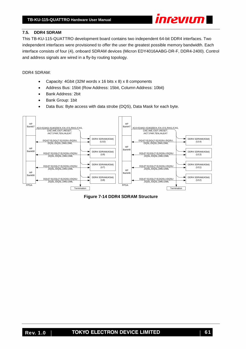
TB-KU-115-QUATTRO Hardware User Manual
61 Rev. 1.0
7.5. DDR4 SDRAM This TB-KU-115-QUATTRO development board contains two independent 64-bit DDR4 interfaces. Two independent interfaces were provisioned to offer the user the greatest possible memory bandwidth. Each interface consists of four (4), onboard SDRAM devices (Micron EDY4016AABG-DR-F, DDR4-2400). Control and address signals are wired in a fly-by routing topology.
DDR4 SDRAM:
• Capacity: 4Gbit (32M words x 16 bits x 8) x 8 components • Address Bus: 15bit (Row Address: 15bit, Column Address: 10bit) • Bank Address: 2bit • Bank Group: 1bit • Data Bus: Byte access with data strobe (DQS), Data Mask for each byte.
DDR4 SDRAM(4Gbit)(U10)
DDR4 SDRAM(4Gbit)(U9)
DQU[7:0],DQL[7:0],DQSU,/DQSU,DQSL,/DQSL,DMU,DML
DDR4 SDRAM(4Gbit)(U7)
DDR4 SDRAM(4Gbit)(U8)
HPBank68
HPBank67
HPBank66
FPGA
DQU[7:0],DQL[7:0],DQSU,/DQSU,DQSL,/DQSL,DMU,DML
DQU[7:0],DQL[7:0],DQSU,/DQSU,DQSL,/DQSL,DMU,DML
DQU[7:0],DQL[7:0],DQSU,/DQSU,DQSL,/DQSL,DMU,DML
Termination
DDR4 SDRAM(4Gbit)(U14)
DDR4 SDRAM(4Gbit)(U13)
DQU[7:0],DQL[7:0],DQSU,/DQSU,DQSL,/DQSL,DMU,DML
A[13:0],BA[1:0],BG[0]CK,/CK,/CS,/RAS,/CAS,CKE,/WE,/ODT,/RESET,/ACT,PAR,TEN,/ALEAT
DDR4 SDRAM(4Gbit)(U11)
DDR4 SDRAM(4Gbit)(U12)
HPBank48
HPBank47
HPBank46
FPGA
DQU[7:0],DQL[7:0],DQSU,/DQSU,DQSL,/DQSL,DMU,DML
DQU[7:0],DQL[7:0],DQSU,/DQSU,DQSL,/DQSL,DMU,DML
DQU[7:0],DQL[7:0],DQSU,/DQSU,DQSL,/DQSL,DMU,DML
Termination
A[13:0],BA[1:0],BG[0]CK,/CK,/CS,/RAS,/CAS,CKE,/WE,/ODT,/RESET,/ACT,PAR,TEN,/ALEAT
Figure 7-14 DDR4 SDRAM Structure
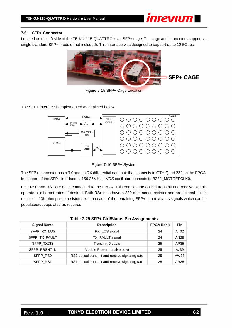
TB-KU-115-QUATTRO Hardware User Manual
62 Rev. 1.0
7.6. SFP+ Connector Located on the left side of the TB-KU-115-QUATTRO is an SFP+ cage. The cage and connectors supports a single standard SFP+ module (not included). This interface was designed to support up to 12.5Gbps.
Figure 7-15 SFP+ Cage Location
The SFP+ interface is implemented as depicted below:
SFP+CONN.
I2CI2C
MUX
FPGA
ZYNQ
TX/RX
156.25MHzXO
LVLSHIFT
STATUSCTRL
CAGE
Figure 7-16 SFP+ System
The SFP+ connector has a TX and an RX differential data pair that connects to GTH Quad 232 on the FPGA. In support of the SFP+ interface, a 156.25MHz, LVDS oscillator connects to B232_MGTREFCLK0.
Pins RS0 and RS1 are each connected to the FPGA. This enables the optical transmit and receive signals operate at different rates, if desired. Both RSx nets have a 330 ohm series resistor and an optional pullup resistor. 10K ohm pullup resistors exist on each of the remaining SFP+ control/status signals which can be populated/depopulated as required.
Table 7-29 SFP+ Ctrl/Status Pin Assignments Signal Name Description FPGA Bank Pin
SFPP_RX_LOS RX_LOS signal 24 AT32
SFPP_TX_FAULT TX_FAULT signal 24 AN29
SFPP_TXDIS Transmit Disable 25 AP35
SFPP_PRSNT_N Module Present (active_low) 25 AJ39
SFPP_RS0 RS0 optical transmit and receive signaling rate 25 AW38
SFPP_RS1 RS1 optical transmit and receive signaling rate 25 AR35
SFP+ CAGE

TB-KU-115-QUATTRO Hardware User Manual
63 Rev. 1.0
7.7. I2C Sub-System Quattro contains several I2C programmable devices. These devices can be mastered by either the FPGA or by the Zynq (PS)8. The following block diagram depicts the I2C structure.
ZYNQ
FPGA
LVLSHIFT
I2CMUX
SC/SD0
SI5338A SI5347A
SC/SD1 SFP+
SC/SD2
SC/SD3
IOEXPANDER
FMC0 FMC1 FMC2 FMC3
MASTER/SLAVE
SLAVE
IOEXPANDER
0x72h
0xE4h
0xE0h 0xD8h
0x74h
SI5338 INTERRUPTPLL[3:0] LOSS OF LOCKQUAD PLL INTERRUPTnQUAD PLL OEnQUAD PLL RESETn
FMC[3:0] PRESENT
FMC[3:0] POWER GOOD
0xA0/A2
xxxxxx00 xxxxxx01 xxxxxx10 xxxxxx11
MASTER/SLAVE
Figure 7-17 I2C Sub-System
An I2C 4:1 Multiplexer (Texas Instruments, PCA9544A) provides address and level shifting isolation between the I2C Master(s) and the downstream Slave devices. The bi-directional multiplexer can direct commands from the Master nus to any one, all, or combination of Slave buses. As the I2C multiplexer is shared with other Kintex/Zynq I2C inter-operation functionality, it is recommended that the address and Read/Write polarity of the multiplexer be left at its factory DEFAULT settings.
The I2C addresses for FMC[3:0] are dependent on the FMC devices, and thus, as per VITA 57.1, Quattro only controls and increments the two LSBs of the FMC I2C address.
Table 7-30 I2C Bus Pin Assignment (FPGA) I2C Signal Name FPGA Bank Pin SCL CLK_FPGA_IO_I2C_OD 64 AF19 SDA SDA_FPGA_IO_I2C_OD 64 AG19
8 multi-master operation is not validated, but is theoretically possible

TB-KU-115-QUATTRO Hardware User Manual
64 Rev. 1.0
Table 7-31 I2C Devices and Addresses I2C Device I2C Address MFR MPN Kintex US Master Programmable Xilinx XCKU115-2FLVA1517C Kintex US Slave Programmable Zynq (PS, MIO) Master/Slave
N/A/Programmable Xilinx XC7Z010-2CLG225I
I2C Multiplexer 0xE4h Texas Instruments TCA9544APW I/O Expander #1 0x72h Texas Instruments PCA9534APWR I/O Expander #2 0x74h Texas Instruments PCA9534APWR SFP+ 0xA0h
0xA2h N/A N/A
Clock Generator 0xE0h Silicon Labs SI5338A Jitter Filter 0xD8h Silicon Labs SI5347A FMC0 xxxxxx00b N/A N/A FMC1 xxxxxx01b N/A N/A FMC2 xxxxxx10b N/A N/A FMC3 xxxxxx11b N/A N/A
7.8. USB to UART Controller (FPGA) The TB-KU-115-QUATTRO features a Silicon Labs CP2103 USB-to-UART interface that enables a PC to communicate with the FPGA. This module creates a virtual COM port on the computer to allow the user to connect through standard USB. The USB interface on this card is Micro USB Type AB which mates with either Micro-A or Micro-B cables.
Table 7-32 Micro-USB Type B and AB Compatibility Receptacle Plug Micro-AB
Micro-A
Micro-B
The UART signals are connected to the FPGA’s single-ended pins on Bank 65. Below is a table indicating where the signals connect. Both the UART transmit and receive data signals are connected as well as flow control signals9. Using the PC’s virtual COM port drivers, there are many different baud rates that are compatible with this controller and can be set during the COM port configuration.
9 Flow control use is optional

TB-KU-115-QUATTRO Hardware User Manual
65 Rev. 1.0
FPGA
CP2103Micro USBConnectorType AB
D+
D-
RXTX MicroUSB
CableRTSCTS
ESDProtection
`
Figure 7-18 USB UART Interface (FPGA)
Table 7-33 UART Interface Pin Assignment Signal FPGA Bank FPGA Pin
UART_TX 65 AE15 UART_RX 65 AL15
UART_RTS_N 65 AM15 UART_CTS_N 65 AW15

TB-KU-115-QUATTRO Hardware User Manual
66 Rev. 1.0
7.9. Battery This board contains an 11.6 mm coin cell battery connected to the VBATT pin which serves as a battery backup supply for the FPGA’s internal volatile memory that stores the key for AES decryption. More information is available in Xilinx’s UltraScale configuration UG570 document. It is possible to monitor the battery’s voltage through test point TP68.
Figure 7-19 Battery Circuit

TB-KU-115-QUATTRO Hardware User Manual
67 Rev. 1.0
7.10. FPGA Configuration Quattro supports three (3) different methods for configuring the FPGA:
1. Dual QSPI Flash 2. JTAG Programming via 14-pin Header/Digilent® JTAG-over-USB
These two programming methods are now discussed.
7.10.1. Dual Quad (x8) SPI Flash
This board has a 256Mbit dual quad SPI flash (x8) memory for FPGA configuration purposes. Please refer to Xilinx’s UltraScale configuration UG570 document on Master SPI Dual Quad (x8) for more information. The multi-I/O SPI Flash memory is used to provide non-volatile code and data storage.
The FPGA Flash can be programmed either through JTAG (using Vivado®) or through the FPGA’s GPIO pins (“UserIO” shown on figure below).
Devices: N25Q256A11EF840E (Micron) 256Mbit, x1/x2/x4/x8 support Devices Data Rate: 108 MHz (maximum) clock frequency in single transfer rate mode
Bank0
Bank65
D00D01D02D03
D04D05D06D07
QSPIN25Q256
QSPIN25Q256
CFGBVS
VCCO HR
VCCO_0
VCCO_65
VoltageDetect2.08V
VCCO HR
VCCO HR
CCLK
VCCO HR1.8V / 2.5V / 3.3V Selectable VCCO HR
CS
VCCO HR
1V8_VCCAUX
LevelshiftTXS0108
Bank47
VCCO
1V2_DDR4
UserIOUserIOUserIOUserIOUserIOUserIO
CS
LevelshiftTXS0108
D00D01D02D03
CCLKCS
OE
OEFET
1V8_VCCAUX
ZYNQ_CFG_OD
1V8_VCCAUX
UserIO
LevelshiftTXS0108
1V8_VCCAUX
1V8_VCCAUX
1V2_DDR4
Figure 7-20 FPGA SPI Flash Configuration Structure In order to pre-configure the flash using the Zynq’s interface via JTAG, it is necessary that the user drives signal SPIFLASH_ZYNQ_CFG_OD “low” prior to programming using JTAG.
• SPIFLASH_ZYNQ_CFG_OD = “high”: Bank 0 used for configuration (default).
• SPIFLASH_ZYNQ_CFG_OD = “low”: Zynq UserIO programs flash through JTAG.
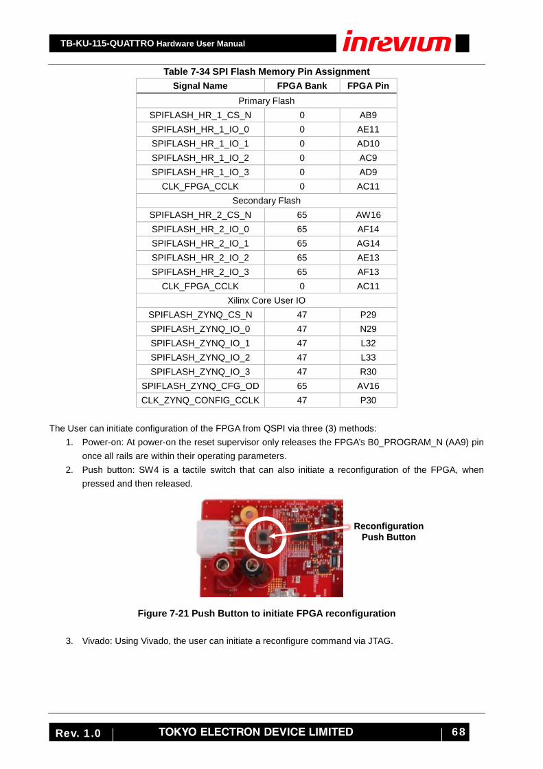
TB-KU-115-QUATTRO Hardware User Manual
68 Rev. 1.0
Table 7-34 SPI Flash Memory Pin Assignment Signal Name FPGA Bank FPGA Pin
Primary Flash SPIFLASH_HR_1_CS_N 0 AB9 SPIFLASH_HR_1_IO_0 0 AE11 SPIFLASH_HR_1_IO_1 0 AD10 SPIFLASH_HR_1_IO_2 0 AC9 SPIFLASH_HR_1_IO_3 0 AD9
CLK_FPGA_CCLK 0 AC11 Secondary Flash
SPIFLASH_HR_2_CS_N 65 AW16 SPIFLASH_HR_2_IO_0 65 AF14 SPIFLASH_HR_2_IO_1 65 AG14 SPIFLASH_HR_2_IO_2 65 AE13 SPIFLASH_HR_2_IO_3 65 AF13
CLK_FPGA_CCLK 0 AC11 Xilinx Core User IO
SPIFLASH_ZYNQ_CS_N 47 P29 SPIFLASH_ZYNQ_IO_0 47 N29 SPIFLASH_ZYNQ_IO_1 47 L32 SPIFLASH_ZYNQ_IO_2 47 L33 SPIFLASH_ZYNQ_IO_3 47 R30
SPIFLASH_ZYNQ_CFG_OD 65 AV16 CLK_ZYNQ_CONFIG_CCLK 47 P30
The User can initiate configuration of the FPGA from QSPI via three (3) methods:
1. Power-on: At power-on the reset supervisor only releases the FPGA’s B0_PROGRAM_N (AA9) pin once all rails are within their operating parameters.
2. Push button: SW4 is a tactile switch that can also initiate a reconfiguration of the FPGA, when pressed and then released.
Figure 7-21 Push Button to initiate FPGA reconfiguration
3. Vivado: Using Vivado, the user can initiate a reconfigure command via JTAG.
Reconfiguration Push Button

TB-KU-115-QUATTRO Hardware User Manual
69 Rev. 1.0
7.10.2. JTAG Programming via 14-pin Header/Digilent® JTAG-over-USB
The TB-KU-115-QUATTRO provides two methods for interfacing to the JTAG port on the FPGA: 14-pin Header, and Digilent JTAG-over-USB.
Figure 7-22 FPGA/ZYNQ JTAG Header Location Note: Do not plug into both interfaces at the same time. Damage should not occur, however, operation could be unpredictable.
Digilent JTAG-over-USB MicroAB USB
(J59)
FPGA/ZYNQ JTAG HEADER
(J32)

TB-KU-115-QUATTRO Hardware User Manual
70 Rev. 1.0
The JTAG chain architecture is shown below.
10Ω
10Ω
10Ω
0Ω
Digilent Module
JTAG HEADER
TDO
TDI
TMS
TCK
FPGA0Ω
0Ω
0Ω
0Ω 0Ω
OPEN
0Ω ZYNQ
0ΩLVL
SHIFT
22Ω
TDO TDI
TMS
TCK
22Ω
TDO
22Ω
Figure 7-23 FPGA/ZYNQ JTAG Chain Architecture
Table 7-35 Xilinx 14-pin JTAG Pinout Pin Xilinx 14-pin JTAG Pin 1 GND VREF 2 3 GND TMS 4 5 GND TCK 6 7 GND TDO 8 9 GND TDI 10 11 GND NC 12 13 GND NC 14
Table 7-36 FPGA Bank 0 JTAG Pin Assignment Signal Name TMS TCK TDO TDI
FPGA Bank 0 Pin W11 AA11 T10 U11 As shown in Figure 7-15 above there are a number of resistors present. The 10Ω resistors provide isolation between the Digilent Module and the JTAG Header. The 22Ω resistors are source terminations. Most importantly, though, the 0Ω and “OPEN” resistors provide a method of removing Zynq from the JTAG chain. As any soldering will void the board warranty, removing components within the chain is only to be done as a last resort. Under normal operation, regardless of whether the Digilent interface or the JTAG header is used, Vivado should detect and display the FPGA and the Zynq in the JTAG block diagram.
7.11. General Purpose LEDs (FPGA) The TB-KU-115-QUATTRO has 8 user programmable LEDs that can be driven by the FPGA. There are 4 green colored LEDs and 4 red ones. The FPGA can be programmed to output a logic “high” to turn “ON” an LED and a logic “low” to turn it “OFF”.
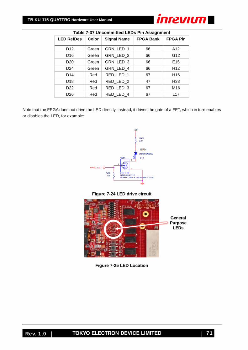
TB-KU-115-QUATTRO Hardware User Manual
71 Rev. 1.0
Table 7-37 Uncommitted LEDs Pin Assignment LED RefDes Color Signal Name FPGA Bank FPGA Pin
D12 Green GRN_LED_1 66 A12 D16 Green GRN_LED_2 66 G12 D20 Green GRN_LED_3 66 E15 D24 Green GRN_LED_4 66 H12 D14 Red RED_LED_1 67 H16 D18 Red RED_LED_2 47 H33 D22 Red RED_LED_3 67 M16 D26 Red RED_LED_4 67 L17
Note that the FPGA does not drive the LED directly, instead, it drives the gate of a FET, which in turn enables or disables the LED, for example:
Figure 7-24 LED drive circuit
Figure 7-25 LED Location
General Purpose
LEDs
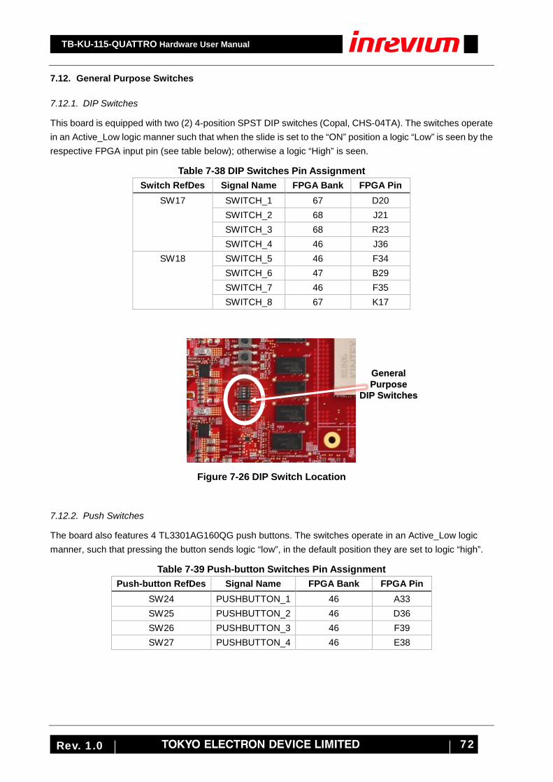
TB-KU-115-QUATTRO Hardware User Manual
72 Rev. 1.0
7.12. General Purpose Switches
7.12.1. DIP Switches
This board is equipped with two (2) 4-position SPST DIP switches (Copal, CHS-04TA). The switches operate in an Active_Low logic manner such that when the slide is set to the “ON” position a logic “Low” is seen by the respective FPGA input pin (see table below); otherwise a logic “High” is seen.
Table 7-38 DIP Switches Pin Assignment Switch RefDes Signal Name FPGA Bank FPGA Pin
SW17 SWITCH_1 67 D20 SWITCH_2 68 J21 SWITCH_3 68 R23 SWITCH_4 46 J36
SW18 SWITCH_5 46 F34 SWITCH_6 47 B29 SWITCH_7 46 F35 SWITCH_8 67 K17
Figure 7-26 DIP Switch Location
7.12.2. Push Switches
The board also features 4 TL3301AG160QG push buttons. The switches operate in an Active_Low logic manner, such that pressing the button sends logic “low”, in the default position they are set to logic “high”.
Table 7-39 Push-button Switches Pin Assignment Push-button RefDes Signal Name FPGA Bank FPGA Pin
SW24 PUSHBUTTON_1 46 A33 SW25 PUSHBUTTON_2 46 D36 SW26 PUSHBUTTON_3 46 F39 SW27 PUSHBUTTON_4 46 E38
General Purpose
DIP Switches

TB-KU-115-QUATTRO Hardware User Manual
73 Rev. 1.0
Figure 7-27 Push Button Switch Location
7.12.3. Jumper Switches
Lastly, 8 jumper switches were conveniently placed at the user’s disposal available as a standard 16-pin header. It provides uncommitted GPOs that connect to the board’s FPGA.
Figure 7-28 Jumper Switches Structure The signals output logic “high” by default (when there is no jumper connected). Connect an odd-numbered pin to the even-numbered pin across from it to output a logic “low” to the FPGA. The header’s reference designator on the board is J42.
Table 7-40 Jumper Switches Pin Assignment Jumper Option Signal Name FPGA Bank FPGA Pin
1-2 HDR1 66 C16 3-4 HDR2 66 H13 5-6 HDR3 66 N13 7-8 HDR4 68 A23 9-10 HDR5 68 C24 11-12 HDR6 68 F22 13-14 HDR7 68 H22 15-16 HDR8 68 L22
General Purpose
Push Buttons

TB-KU-115-QUATTRO Hardware User Manual
74 Rev. 1.0
Figure 7-29 Jumper Switches Location
Jumper Switches
PIN 1 PIN 3

TB-KU-115-QUATTRO Hardware User Manual
75 Rev. 1.0
7.13. Zynq Sub-System In addition to the Kintex UltraScale KU115 device, Quattro also contains a Zynq-7000 SoC. The ZC7Z010, provides an additional method for programming the peripheral devices on board. The Zynq sub-system architecture is shown below.
FLASH
USB-to-UART
ZYNQ
XC7Z010-2CLG225I
I2C MUX
MASTER/SLAVE
JTAG HEADER
uSD SLOT
USB MicroAB
General Purpose DIP
Switches General Purpose
LEDs
0 0 0
1 1 1
0
1
MIO
MIO
MIO
MIO MIO MIO
MIO
GPIO
BA
NK
34
FPGA
MASTER/SLAVE
12
8BANK 67
BANK 47
GPIO
SVSR
POR
from UCD9090
Push Button Reset
Config.Jumpers
Figure 7-30 Zynq Sub-System Architecture
Figure 7-31 Zynq Sub-System Photo
PLL BYPASS
JTAG MODE BOOT MODE
uSD SLOT
RESET SWITCH
DIP SWITCHES
USB over UART
JTAG HEADER
LEDs
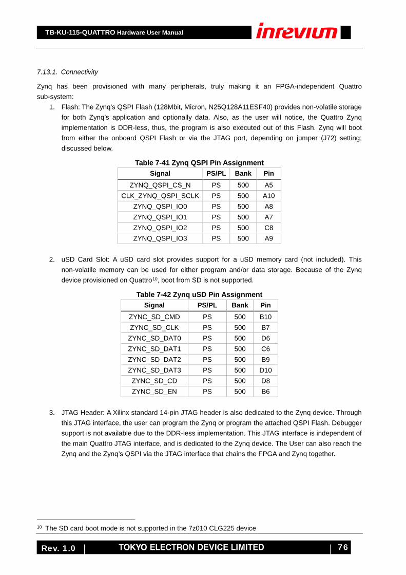
TB-KU-115-QUATTRO Hardware User Manual
76 Rev. 1.0
7.13.1. Connectivity
Zynq has been provisioned with many peripherals, truly making it an FPGA-independent Quattro sub-system:
1. Flash: The Zynq’s QSPI Flash (128Mbit, Micron, N25Q128A11ESF40) provides non-volatile storage for both Zynq’s application and optionally data. Also, as the user will notice, the Quattro Zynq implementation is DDR-less, thus, the program is also executed out of this Flash. Zynq will boot from either the onboard QSPI Flash or via the JTAG port, depending on jumper (J72) setting; discussed below.
Table 7-41 Zynq QSPI Pin Assignment Signal PS/PL Bank Pin
ZYNQ_QSPI_CS_N PS 500 A5 CLK_ZYNQ_QSPI_SCLK PS 500 A10
ZYNQ_QSPI_IO0 PS 500 A8 ZYNQ_QSPI_IO1 PS 500 A7 ZYNQ_QSPI_IO2 PS 500 C8 ZYNQ_QSPI_IO3 PS 500 A9
2. uSD Card Slot: A uSD card slot provides support for a uSD memory card (not included). This
non-volatile memory can be used for either program and/or data storage. Because of the Zynq device provisioned on Quattro10, boot from SD is not supported.
Table 7-42 Zynq uSD Pin Assignment Signal PS/PL Bank Pin
ZYNC_SD_CMD PS 500 B10 ZYNC_SD_CLK PS 500 B7
ZYNC_SD_DAT0 PS 500 D6 ZYNC_SD_DAT1 PS 500 C6 ZYNC_SD_DAT2 PS 500 B9 ZYNC_SD_DAT3 PS 500 D10 ZYNC_SD_CD PS 500 D8 ZYNC_SD_EN PS 500 B6
3. JTAG Header: A Xilinx standard 14-pin JTAG header is also dedicated to the Zynq device. Through
this JTAG interface, the user can program the Zynq or program the attached QSPI Flash. Debugger support is not available due to the DDR-less implementation. This JTAG interface is independent of the main Quattro JTAG interface, and is dedicated to the Zynq device. The User can also reach the Zynq and the Zynq’s QSPI via the JTAG interface that chains the FPGA and Zynq together.
10 The SD card boot mode is not supported in the 7z010 CLG225 device

TB-KU-115-QUATTRO Hardware User Manual
77 Rev. 1.0
Table 7-43 Zynq PL JTAG Header Pin Assignment Signal PS/PL Bank Pin
CLK_ZYNQ_TCK_FABRIC PL 34 R13 ZYNQ_TMS_FABRIC PL 34 P13 ZYNQ_TDI_FABRIC PL 34 P14 ZYNQ_TDO_FABRIC PL 34 M9
4. USB (UART over USB): The Zynq sub-system can also communicate with a PC, or other, via a
UART over USB interface. This interface is comprised of a USB MicroAB connector and a USB-to-UART converter chip (SiLabs, CP2103), whose logic level outputs connect directly to MIO pins on the Zynq device. This is simply a two (2) wire UART interface, and thus, hardware flow control is not supported.
Table 7-44 Zynq UART Pin Assignment Signal PS/PL Bank Pin
USB_UART_ZYNQ_TX PS 501 C12 USB_UART_ZYNQ_RX PS 501 B15
5. General purpose DIP Switches: Four (4) general purpose DIP switches are connected to MIO pins
of the Zynq. These DIP switches are not assigned, and can be used for user application.
Table 7-45 Zynq GP DIP Switch Pin Assignment Signal PS/PL Bank Pin
ZYNQ_SW0 PS 501 E15 ZYNQ_SW1 PS 501 C11 ZYNQ_SW2 PS 501 D15 ZYNQ_SW3 PS 501 A14
6. General purpose LEDs: Six (8) LEDs, consisting of four (5) green and two (3) red LEDs, are unassigned, and can be used for user application.
Table 7-46 Zynq GP LED Pin Assignment Signal PS/PL Bank Pin
ZYNQ_GN1 PS 501 A13 ZYNQ_GN2 PS 501 D14 ZYNQ_GN3 PS 501 B21 ZYNQ_GN4 PS 501 D13 ZYNQ_RD1 PS 501 A12 ZYNQ_RD2 PS 501 C13
ZYNC_GREEN_LED PL 34 R10 ZYNC_RED_LED PL 34 P10
7. I2C Interface: The Zynq provides an ARM™-based method for controlling the I2C programmable
devices onboard Quattro. As discussed earlier, either the Zynq or the FPGA can master this I2C bus. Also note, as per Figure 7-12, when Zynq is mastering the I2C bus, it can communicate with the FPGA if the FPGA includes a Slave interface. This capability enables the user to mimic an

TB-KU-115-QUATTRO Hardware User Manual
78 Rev. 1.0
end-system application where a microprocessor is used to supervise an FPGA.
Table 7-47 Zynq I2C Pin Assignment Signal PS/PL Bank Pin
CLK_ZYNQ_I2C_SCL_OD PS 501 A15 ZYNQ_I2C_SDA_OD PS 501 D11
ZYNQ_I2C_INT_N PS 501 C14
8. GPIO: A total of 20 GPIOs connect the Programmable Logic (PL) portion of the Zynq to the FPGA. To support greater bandwidths, these signals are provisioned as 10 differential pairs11. Admittedly, the bank assignments and pinout of these signals on the FPGA is less than ideal, due to the fact that the FPGA pinout was optimized for the FMC ports and other FPGA peripherals. The banks that support this DC-coupled GPIO interface are powered on both the Zynq and the FPGA by 1.2V.
Table 7-48 Zynq GPIO Pin Assignment Signal PS/PL Bank Pin
ZYNQ_GPIO_0_P PL 34 P8 ZYNQ_GPIO_0_N PL 34 P9 ZYNQ_GPIO_1_P PL 34 G11 ZYNQ_GPIO_1_N PL 34 H12 ZYNQ_GPIO_2_P PL 34 G12 ZYNQ_GPIO_2_N PL 34 H13 ZYNQ_GPIO_3_P PL 34 J15 ZYNQ_GPIO_3_N PL 34 K15 ZYNQ_GPIO_4_P PL 34 J13 ZYNQ_GPIO_4_N PL 34 J14 ZYNQ_GPIO_5_P PL 34 N13 ZYNQ_GPIO_5_N PL 34 N14 ZYNQ_GPIO_6_P PL 34 L15 ZYNQ_GPIO_6_N PL 34 M15 ZYNQ_GPIO_7_P PL 34 K11 ZYNQ_GPIO_7_N PL 34 K12 ZYNQ_GPIO_8_P PL 34 P11 ZYNQ_GPIO_8_N PL 34 R11 ZYNQ_GPIO_9_P PL 34 N7 ZYNQ_GPIO_9_N PL 34 N8
7.13.2. Power-On Reset and Jumper-based Configuration
At power-on a dedicated reset supervisor and the UCD9090 hold Zynq’s power-on-reset (POR) signal low, until all rails have stabilized, after which POR is released, and Zynq is allowed to boot. Tactile switch (SW23) allows the user to either hold off boot at power-on or initiate a power-on-reset as well. 11 20 signals total. Nothing precludes single ended operation

TB-KU-115-QUATTRO Hardware User Manual
79 Rev. 1.0
Zynq is provisioned with three (3) jumpers that control Zynq’s method and boot-time configuration. These are sampled during POR. Each header can be provisioned in one of two positions.
Table 7-49 Zynq Boot Mode Configuration Header Description Jumper Position J74 MIO[6]
Zynq PLL 1-2: PLL Bypassed 2-3: PLL Enabled (default)
J75 MIO[2]
Zynq JTAG Mode
1-2: Independent; Zynq-dedicated JTAG header accesses DAP only, but user must first route DAP to SelectIO. TAP remains available through the dedicated JTAG pins. 2-3: Cascade (default); Connect to both TAP/DAP through the Zynq-dedicated JTAG header
J72 MIO[4]
Zynq Boot Source 1-2: uSD Card (NOT SUPPORTED) 2-3: QSPI (default) 2-3: JTAG (R937, R942 need to be swapped)
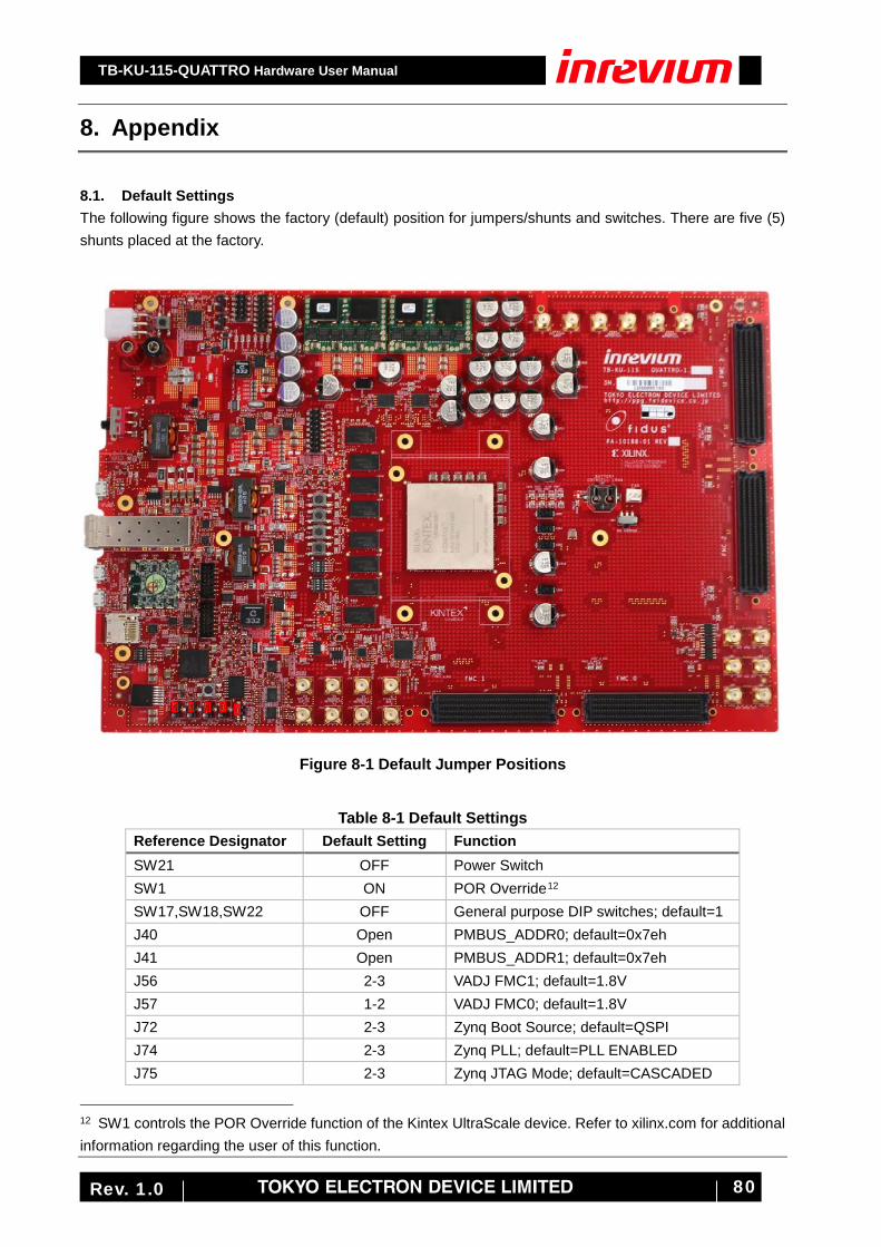
TB-KU-115-QUATTRO Hardware User Manual
80 Rev. 1.0
8. Appendix
8.1. Default Settings The following figure shows the factory (default) position for jumpers/shunts and switches. There are five (5) shunts placed at the factory.
Figure 8-1 Default Jumper Positions
Table 8-1 Default Settings Reference Designator Default Setting Function SW21 OFF Power Switch SW1 ON POR Override12 SW17,SW18,SW22 OFF General purpose DIP switches; default=1 J40 Open PMBUS_ADDR0; default=0x7eh J41 Open PMBUS_ADDR1; default=0x7eh J56 2-3 VADJ FMC1; default=1.8V J57 1-2 VADJ FMC0; default=1.8V J72 2-3 Zynq Boot Source; default=QSPI J74 2-3 Zynq PLL; default=PLL ENABLED J75 2-3 Zynq JTAG Mode; default=CASCADED
12 SW1 controls the POR Override function of the Kintex UltraScale device. Refer to xilinx.com for additional information regarding the user of this function.

TB-KU-115-QUATTRO Hardware User Manual
81 Rev. 1.0
8.2. Texas Instruments, UCD9090, Power Sequencer The UCD9090 is a programmable power monitor and sequencer that has been configured to sequence, monitor, and control the various power supplies on Quattro. There are four (4) headers and one (1) switch associated with the power sequencers:
Table 8-2 Power Sequencer Reference Designator Function SW21 Power Switch J40, J41 PMBus Address LSBs J39 PMBus Header J38 UCD9090 JTAG Programming Header
Figure 8-2 UCD9090 Headers Note: The user should never have to access or modify the factory programming of the UCD9090. Doing so could cause irreparable damage and void the warranty. Note: The UCD9090 JTAG Programming Header (J38) is for factory use only.
JTAG HEADER
PMBUS HEADER PMBUS ADDRESS LSBs

TB-KU-115-QUATTRO Hardware User Manual
82 Rev. 1.0
Inrevium Company URL: http://solutions.inrevium.com/ http://solutions.inrevium.com/jp/ E-mail: [email protected] HEAD Quarter: Yokohama East Square, 1-4 Kinko-cho, Kanagawa-ku, Yokohama City,
Kanagawa, Japan 221-0056 TEL: +81-45-443-4031 FAX: +81-45-443-4063