symphony dsp56720 and dsp56721 multi-core … · symphony ™ dsp56720/dsp56721 ... p x y on-chip...
TRANSCRIPT
Freescale SemiconductorData Sheet: Technical Data
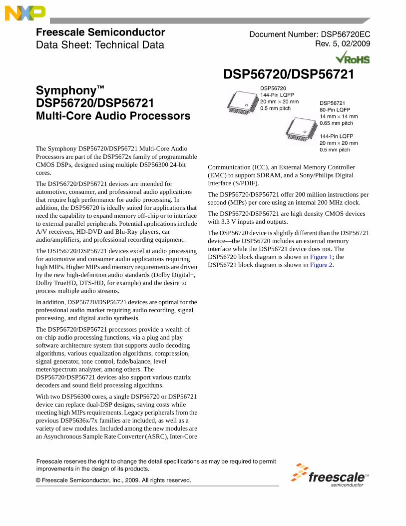
DSP56720/DSP56721DSP56720144-Pin LQFP20 mm × 20 mm0.5 mm pitch
DSP5672180-Pin LQFP14 mm × 14 mm0.65 mm pitch
144-Pin LQFP20 mm × 20 mm0.5 mm pitch
Document Number: DSP56720ECRev. 5, 02/2009
Symphony™ DSP56720/DSP56721 Multi-Core Audio Processors
The Symphony DSP56720/DSP56721 Multi-Core Audio Processors are part of the DSP5672x family of programmable CMOS DSPs, designed using multiple DSP56300 24-bit cores.
The DSP56720/DSP56721 devices are intended for automotive, consumer, and professional audio applications that require high performance for audio processing. In addition, the DSP56720 is ideally suited for applications that need the capability to expand memory off-chip or to interface to external parallel peripherals. Potential applications include A/V receivers, HD-DVD and Blu-Ray players, car audio/amplifiers, and professional recording equipment.
The DSP56720/DSP56721 devices excel at audio processing for automotive and consumer audio applications requiring high MIPs. Higher MIPs and memory requirements are driven by the new high-definition audio standards (Dolby Digital+, Dolby TrueHD, DTS-HD, for example) and the desire to process multiple audio streams.
In addition, DSP56720/DSP56721 devices are optimal for the professional audio market requiring audio recording, signal processing, and digital audio synthesis.
The DSP56720/DSP56721 processors provide a wealth of on-chip audio processing functions, via a plug and play software architecture system that supports audio decoding algorithms, various equalization algorithms, compression, signal generator, tone control, fade/balance, level meter/spectrum analyzer, among others. The DSP56720/DSP56721 devices also support various matrix decoders and sound field processing algorithms.
With two DSP56300 cores, a single DSP56720 or DSP56721 device can replace dual-DSP designs, saving costs while meeting high MIPs requirements. Legacy peripherals from the previous DSP5636x/7x families are included, as well as a variety of new modules. Included among the new modules are an Asynchronous Sample Rate Converter (ASRC), Inter-Core
© Freescale Semiconductor, Inc., 2009. All rights reserved.
Freescale reserves the right to change the detail specifications aimprovements in the design of its products.
Communication (ICC), an External Memory Controller (EMC) to support SDRAM, and a Sony/Philips Digital Interface (S/PDIF).
The DSP56720/DSP56721 offer 200 million instructions per second (MIPs) per core using an internal 200 MHz clock.
The DSP56720/DSP56721 are high density CMOS devices with 3.3 V inputs and outputs.
The DSP56720 device is slightly different than the DSP56721 device—the DSP56720 includes an external memory interface while the DSP56721 device does not. The DSP56720 block diagram is shown in Figure 1; the DSP56721 block diagram is shown in Figure 2.
s may be required to permit

Table of Contents1 Pin Assignments . . . . . . . . . . . . . . . . . . . . . . . . . . . . . . . . . . . .4
1.1 Pinout for DSP56720 144-Pin Plastic LQFP Package . .51.2 Pinout for DSP56721 80-Pin Plastic LQFP Package . . .61.3 Pinout for DSP56721 144-Pin Plastic LQFP Package . .71.4 Pin Multiplexing. . . . . . . . . . . . . . . . . . . . . . . . . . . . . . . .7
2 Electrical Characteristics . . . . . . . . . . . . . . . . . . . . . . . . . . . . .82.1 Maximum Ratings . . . . . . . . . . . . . . . . . . . . . . . .82.2 Thermal Characteristics. . . . . . . . . . . . . . . . . . . .92.3 Power Requirements . . . . . . . . . . . . . . . . . . . . .102.5 DC Electrical Characteristics . . . . . . . . . . . . . . .122.6 AC Electrical Characteristics . . . . . . . . . . . . . . .132.7 Internal Clocks. . . . . . . . . . . . . . . . . . . . . . . . . .132.8 External Clock Operation. . . . . . . . . . . . . . . . . .132.9 Reset, Stop, Mode Select, and Interrupt Timing 152.10 Serial Host Interface (SHI) SPI Protocol Timing 182.11 Serial Host Interface (SHI) I2C Protocol Timing.24
2.12 Programming the SHI I2C Serial Clock . . . . . . 262.13 Enhanced Serial Audio Interface (ESAI) Timing272.14 Timer Timing . . . . . . . . . . . . . . . . . . . . . . . . . . 322.15 GPIO Timing . . . . . . . . . . . . . . . . . . . . . . . . . . 322.16 JTAG Timing. . . . . . . . . . . . . . . . . . . . . . . . . . . 332.17 Watchdog Timer Timing . . . . . . . . . . . . . . . . . . 352.18 Host Data Interface (HDI24) Timing. . . . . . . . . 352.19 S/PDIF Timing . . . . . . . . . . . . . . . . . . . . . . . . . 422.20 EMC Timing (DSP56720 Only) . . . . . . . . . . . . 43
3 Functional Description and Application Information . . . . . . . 474 Ordering Information . . . . . . . . . . . . . . . . . . . . . . . . . . . . . . . 485 Package Information . . . . . . . . . . . . . . . . . . . . . . . . . . . . . . . 48
5.1 80-Pin Package Outline Drawing. . . . . . . . . . . . . . . . . 495.2 144-Pin Package Outline Drawing. . . . . . . . . . . . . . . . 51
6 Product Documentation. . . . . . . . . . . . . . . . . . . . . . . . . . . . . 537 Revision History . . . . . . . . . . . . . . . . . . . . . . . . . . . . . . . . . . 53
Symphony™ DSP56720/DSP56721 Multi-Core Audio Processors, Rev. 5
Freescale Semiconductor2

Figure 1. DSP56720 Block Diagram
Figure 2. DSP56721 Block Diagram
SH
I
TE
C
ES
AI
ES
AI_
1
WD
T
GP
IO
SH
I_1
TE
C_1
ES
AI_
2
ES
AI_
3
WD
T_1
GP
IO
PCU / AGU / ALU
DMA OnCE OnCEPCU / AGU / ALU
DMA
On-Chip Memory
P X Y
On-Chip Memory
P X Y
DSP Core-0
EM
C
S/P
DIF
GP
IO
ASRC
Arbiter 8
Arbiters 0–7
2 JTAGs
Shared Memory 8 KbytesBlocks 0–7 (64 Kbytes total)
MODA1, MODB1,MODC1, MODD1
MODA0, MODB0,MODC0, MODD0
JTAG
EXTAL/XTAL
DSP Core-1
Chi
p C
onfig
Arbiter 9
CGM
Shared Bus 0Shared Bus 1
SH
I
TIM
ER
ES
AI
ES
AI_
1
WD
T
GP
IO
HD
I24
SH
I_1
TIM
ER
_1
ES
AI_
2
ES
AI_
3
WD
T_1
GP
IO
HD
I24_
1
PCU / AGU / ALU
DMA OnCE OnCEPCU / AGU / ALU
DMA
On-Chip Memory
P X Y
On-Chip Memory
P X Y
DSP Core-0
SP
DIF
GP
IO
ASRC
Arbiter 8
Arbiters 0–7
2 JTAGs
Shared Memory 8 KbytesBlocks 0–7 (64 Kbytes total)
MODA1, MODB1,MODC1, MODD1
MODA0, MODB0,MODC0, MODD0
JTAG
HDI24 EXTAL/XTAL
DSP Core-1
Chi
p C
onfig
CGM
Shared Bus 0 Shared Bus 1
Symphony™ DSP56720/DSP56721 Multi-Core Audio Processors, Rev. 5
Freescale Semiconductor 3

1 Pin AssignmentsDSP56720 devices are available in one package type; DSP56721 devices are available in two package types. For the pin assignments of a specific device in a specific package, refer to Section 1.1, “Pinout for DSP56720 144-Pin Plastic LQFP Package,” through Section 1.3, “Pinout for DSP56721 144-Pin Plastic LQFP Package.”
For more detailed information about signals, refer to the Symphony™ DSP56720/DSP56721 Multi-Core Audio Processors Reference Manuall (DSP56720RM).
Table 1. Pin Assignments by Package
Device Package See
DSP56720 144-pin plastic LQFP Figure 3 on page 5
DSP56721 80-pin plastic LQFP Figure 4 on page 6
144-pin plastic LQFP Figure 5 on page 7
Symphony™ DSP56720/DSP56721 Multi-Core Audio Processors, Rev. 5
Freescale Semiconductor4
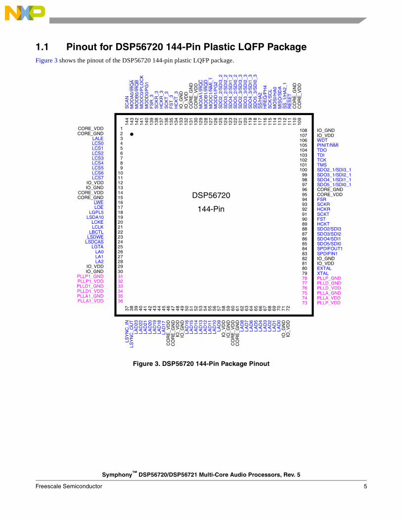
1.1 Pinout for DSP56720 144-Pin Plastic LQFP PackageFigure 3 shows the pinout of the DSP56720 144-pin plastic LQFP package.
Figure 3. DSP56720 144-Pin Package Pinout
108 IO_GND107 IO_VDD106 WDT105 PINIT/NMI104 TDO103 TDI102 TCK101 TMS100 SDO2_1/SDI3_199 SDO3_1/SDI2_198 SDO4_1/SDI1_197 SDO5_1/SDI0_196 CORE_GND95 CORE_VDD94 FSR93 SCKR92 HCKR91 SCKT90 FST89 HCKT88 SDO2/SDI387 SDO3/SDI286 SDO4/SDI185 SDO5/SDI084 SPDIFOUT183 SPDIFIN182 IO_GND81 IO_VDD80 EXTAL79 XTAL78 PLLP_GND77 PLLD_GND76 PLLD_VDD75 PLLA_GND74 PLLA_VDD73 PLLP_VDD
LSY
NC
_IN
37
LS
YN
C_
OU
T3
8LA
D23
39
LAD
224
0LA
D21
41
LAD
204
2LA
D19
43
LAD
184
4 L
AD
17
45
CO
RE
_V
DD
46
CO
RE
_GN
D4
7IO
_V
DD
48
IO_G
ND
49
LAD
165
0LA
D15
51
LAD
145
2LA
D13
53
LAD
125
4LA
D11
55
LAD
105
6LA
D9
57
IO_
VD
D5
8IO
_GN
D5
9C
OR
E_
VD
D6
0C
OR
E_G
ND
61
LAD
86
2LA
D7
63
LAD
66
4LA
D5
65
LAD
46
6LA
D3
67
LAD
26
8LA
D1
69
LAD
07
0IO
_GN
D7
1IO
_V
DD
72
CORE_VDD 1CORE_GND 2
LALE 3LCS0 4LCS1 5LCS2 6LCS3 7LCS4 8LCS5 9LCS6 10LCS7 11
IO_VDD 12IO_GND 13
CORE_VDD 14CORE_GND 15
LWE 16LOE 17
LGPL5 18LSDA10 19
LCKE 20LCLK 21
LBCTL 22LSDWE 23
LSDCAS 24LGTA 25
LA0 26LA1 27LA2 28
IO_VDD 29IO_GND 30
PLLP1_GND 31PLLP1_VDD 32PLLD1_GND 33PLLD1_VDD 34PLLA1_GND 35PLLA1_VDD 36
144
SC
AN
143
MO
DA
0/IR
QA
142
MO
DB
0/IR
QB
141
MO
DC
0/P
LOC
K14
0M
OD
D0/
PG
113
9F
SR
_313
8S
CK
R_3
137
HC
KR
_3
136
SC
KT
_313
5F
ST
_313
4H
CK
T_3
133
IO_G
ND
132
IO_V
DD
131
CO
RE
_GN
D13
0C
OR
E_V
DD
129
MO
DA
1/IR
QC
128
MO
DB
1/IR
QD
127
MO
DC
1/N
MI_
112
6M
OD
D1/
PG
212
5S
DO
2_2
/SD
I3_
212
4S
DO
3_2
/SD
I2_
212
3S
DO
4_2
/SD
I1_
212
2S
DO
5_2
/SD
I0_
212
1S
DO
2_3
/SD
I3_
312
0S
DO
3_3
/SD
I2_
311
9S
DO
4_3
/SD
I1_
311
8S
DO
5_3
/SD
I0_
311
7S
S/H
A2
116
HR
EQ
/PH
411
5S
CK
/SC
L11
4M
OS
I/H
A0
113
MIS
O/S
DA
112
SS
_1/H
A2_
111
1R
ES
ET
110
CO
RE
_GN
D10
9C
OR
E_V
DD
DSP56720
144-Pin
Symphony™ DSP56720/DSP56721 Multi-Core Audio Processors, Rev. 5
Freescale Semiconductor 5
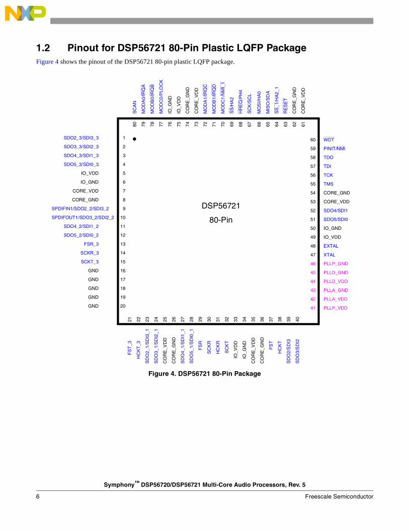
1.2 Pinout for DSP56721 80-Pin Plastic LQFP PackageFigure 4 shows the pinout of the DSP56721 80-pin plastic LQFP package.
Figure 4. DSP56721 80-Pin Package
60 WDT
59 PINIT/NMI
58 TDO
57 TDI
56 TCK
55 TMS
54 CORE_GND
53 CORE_VDD
52 SDO4/SDI1
51 SDO5/SDI0
50 IO_GND
49 IO_VDD
48 EXTAL
47 XTAL
46 PLLP_GND
45 PLLD_GND
44 PLLD_VDD
43 PLLA_GND
42 PLLA_VDD
41 PLLP_VDD
FS
T_3
21
HC
KT
_322
SD
O2_
1/S
DI3
_1
23
SD
O3_
1/S
DI2
_1
24
CO
RE
_VD
D25
CO
RE
_GN
D26
SD
O4_
1/S
DI1
_1
27
SD
O5_
1/S
DI0
_1
28
FS
R29
SC
KR
30
HC
KR
31
SC
KT
32
IO_V
DD
33
IO_G
ND
34
CO
RE
_VD
D35
CO
RE
_GN
D36
FS
T37
HC
KT
38
SD
O2/
SD
I339
SD
O3/
SD
I240
SDO2_3/SDI3_3 1
SDO3_3/SDI2_3 2
SDO4_3/SDI1_3 3
SDO5_3/SDI0_3 4
IO_VDD 5
IO_GND 6
CORE_VDD 7
CORE_GND 8
SPDIFIN1/SDO2_2/SDI3_2 9
SPDIFOUT1/SDO3_2/SDI2_2 10
SDO4_2/SDI1_2 11
SDO5_2/SDI0_2 12
FSR_3 13
SCKR_3 14
SCKT_3 15
GND 16
GND 17
GND 18
GND 19
GND 20
80S
CA
N
79M
OD
A0/
IRQ
A
78M
OD
B0/
IRQ
B
77M
OD
C0
/PLO
CK
76IO
_GN
D
75IO
_VD
D
74C
OR
E_G
ND
73C
OR
E_V
DD
72M
OD
A1/
IRQ
C
71M
OD
B1/
IRQ
D
70M
OD
C1
/NM
I_1
69S
S/H
A2
68H
RE
Q/P
H4
67S
CK
/SC
L
66M
OS
I/HA
0
65M
ISO
/SD
A
64S
S_
1 /H
A2_
1
63R
ES
ET
62C
OR
E_G
ND
61C
OR
E_V
DD
DSP56721
80-Pin
Symphony™ DSP56720/DSP56721 Multi-Core Audio Processors, Rev. 5
Freescale Semiconductor6
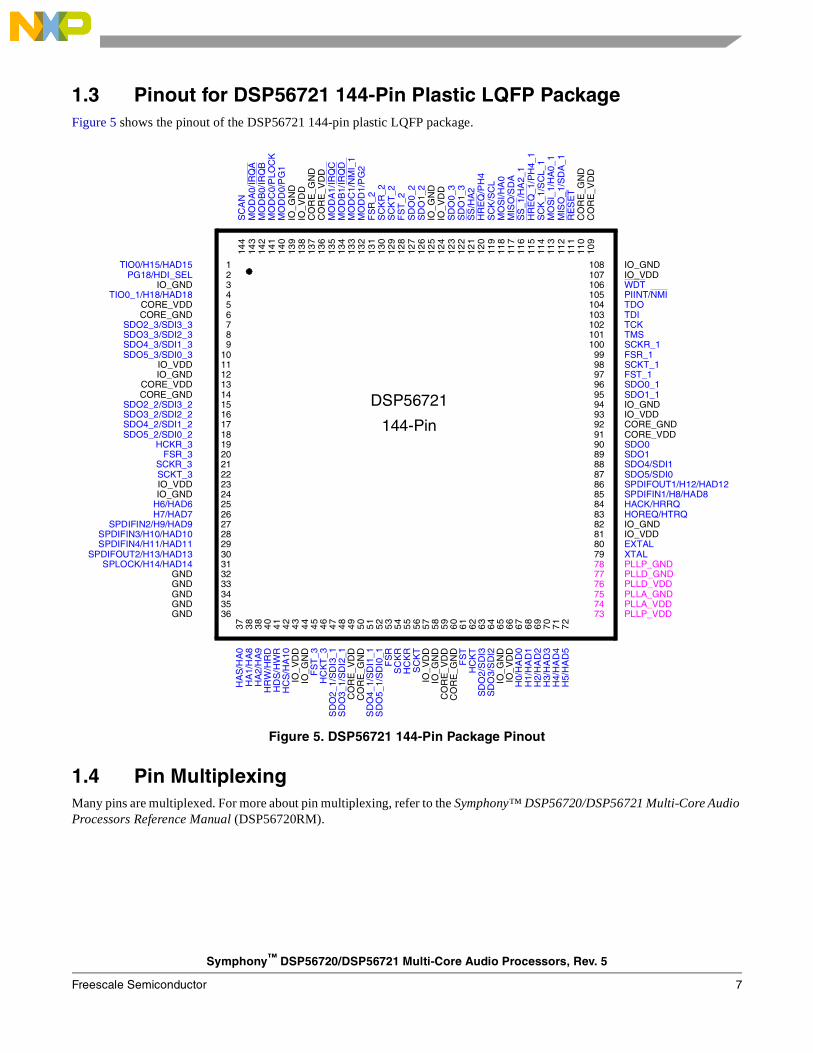
1.3 Pinout for DSP56721 144-Pin Plastic LQFP PackageFigure 5 shows the pinout of the DSP56721 144-pin plastic LQFP package.
Figure 5. DSP56721 144-Pin Package Pinout
1.4 Pin MultiplexingMany pins are multiplexed. For more about pin multiplexing, refer to the Symphony™ DSP56720/DSP56721 Multi-Core Audio Processors Reference Manual (DSP56720RM).
108 IO_GND107 IO_VDD106 WDT105 PIINT/NMI104 TDO103 TDI102 TCK101 TMS100 SCKR_199 FSR_198 SCKT_197 FST_196 SDO0_195 SDO1_194 IO_GND93 IO_VDD92 CORE_GND91 CORE_VDD90 SDO089 SDO188 SDO4/SDI187 SDO5/SDI086 SPDIFOUT1/H12/HAD1285 SPDIFIN1/H8/HAD884 HACK/HRRQ83 HOREQ/HTRQ82 IO_GND81 IO_VDD80 EXTAL79 XTAL78 PLLP_GND77 PLLD_GND76 PLLD_VDD75 PLLA_GND74 PLLA_VDD73 PLLP_VDD
HA
S/H
A0
37
HA
1/H
A8
38
HA
2/H
A9
38
HR
W/H
RD
40
HD
S/H
WR
41
HC
S/H
A10
42
IO_
VD
D4
3IO
_GN
D4
4F
ST
_34
5H
CK
T_3
46
SD
O2
_1/S
DI3
_14
7S
DO
3_1
/SD
I2_1
48
CO
RE
_V
DD
49
CO
RE
_GN
D5
0S
DO
4_1
/SD
I1_1
51
SD
O5
_1/S
DI0
_15
2F
SR
53
SC
KR
54
HC
KR
55
SC
KT
56
IO_
VD
D5
7IO
_GN
D5
8C
OR
E_
VD
D5
9C
OR
E_G
ND
60
FS
T6
1H
CK
T6
2S
DO
2/S
DI3
63
SD
O3/
SD
I26
4IO
_GN
D6
5IO
_V
DD
66
H0/
HA
D0
67
H1/
HA
D1
68
H2/
HA
D2
69
H3/
HA
D3
70
H4/
HA
D4
71
H5/
HA
D5
72
TIO0/H15/HAD15 1PG18/HDI_SEL 2
IO_GND 3TIO0_1/H18/HAD18 4
CORE_VDD 5CORE_GND 6
SDO2_3/SDI3_3 7SDO3_3/SDI2_3 8SDO4_3/SDI1_3 9SDO5_3/SDI0_3 10
IO_VDD 11IO_GND 12
CORE_VDD 13CORE_GND 14
SDO2_2/SDI3_2 15SDO3_2/SDI2_2 16SDO4_2/SDI1_2 17SDO5_2/SDI0_2 18
HCKR_3 19FSR_3 20
SCKR_3 21SCKT_3 22IO_VDD 23IO_GND 24
H6/HAD6 25H7/HAD7 26
SPDIFIN2/H9/HAD9 27SPDIFIN3/H10/HAD10 28SPDIFIN4/H11/HAD11 29
SPDIFOUT2/H13/HAD13 30SPLOCK/H14/HAD14 31
GND 32GND 33GND 34GND 35GND 36
144
SC
AN
143
MO
DA
0/IR
QA
142
MO
DB
0/IR
QB
141
MO
DC
0/P
LOC
K14
0M
OD
D0/
PG
113
9IO
_GN
D13
8IO
_VD
D13
7C
OR
E_G
ND
136
CO
RE
_VD
D13
5M
OD
A1/
IRQ
C13
4M
OD
B1/
IRQ
D13
3M
OD
C1/
NM
I_1
132
MO
DD
1/P
G2
131
FS
R_2
130
SC
KR
_212
9S
CK
T_2
128
FS
T_2
127
SD
O0_
212
6S
DO
1_2
125
IO_G
ND
124
IO_V
DD
123
SD
O0_
312
2S
DO
1_3
121
SS
/HA
212
0H
RE
Q/P
H4
119
SC
K/S
CL
118
MO
SI/H
A0
117
MIS
O/S
DA
116
SS
_1/H
A2_
111
5H
RE
Q_1
/PH
4_1
114
SC
K_1
/SC
L_1
113
MO
SI_
1/H
A0_
111
2M
ISO
_1/
SD
A_1
111
RE
SE
T11
0C
OR
E_G
ND
109
CO
RE
_VD
D
DSP56721
144-Pin
Symphony™ DSP56720/DSP56721 Multi-Core Audio Processors, Rev. 5
Freescale Semiconductor 7

2 Electrical Characteristics
2.1 Maximum RatingsTable 2 shows the maximum ratings.
CAUTIONThis device contains circuitry protecting against damage due to high static voltage or electrical fields. However, normal precautions should be taken to avoid exceeding maximum voltage ratings. Reliability of operation is enhanced if unused inputs are pulled to an appropriate logic voltage level (for example, either GND or VDD). The suggested value for a pull-up or pull-down resistor is 4.7 kΩ.
NOTEIn the calculation of timing requirements, adding a maximum value of one specification to a minimum value of another specification does not yield a reasonable sum. A maximum specification is calculated using a worst case variation of process parameter values in one direction. The minimum specification is calculated using the worst case for the same parameters in the opposite direction. Therefore, a “maximum” value for a specification will never occur in the same device that has a “minimum” value for another specification; adding a maximum to a minimum represents a condition that can never exist.
Table 2. Maximum Ratings
Rating1 Symbol Value1, 2 Unit
Supply Voltage VCORE_VDD, VPLLD_VDD
–0.3 to + 1.26 V
VPLLP_VDD, VIO_VDD,
VPLLA_VDD,–0.3 to + 4.0 V
Maximum CORE_VDD power supply ramp time3 Tr 10 ms
Input Voltage per pin excluding VDD and GND VIN GND –0.3 to 5.5 V V
Current drain per pin excluding VDD and GND (Except for pads listed below)
I 12 mA
LSYNC_OUT Ilsync_out 16 mA
LCLK Ilclk 16 mA
LALE Iale 16 mA
TDO IJTAG 24 mA
Operating temperature range TJ –40 to +100 °C
Symphony™ DSP56720/DSP56721 Multi-Core Audio Processors, Rev. 5
Freescale Semiconductor8
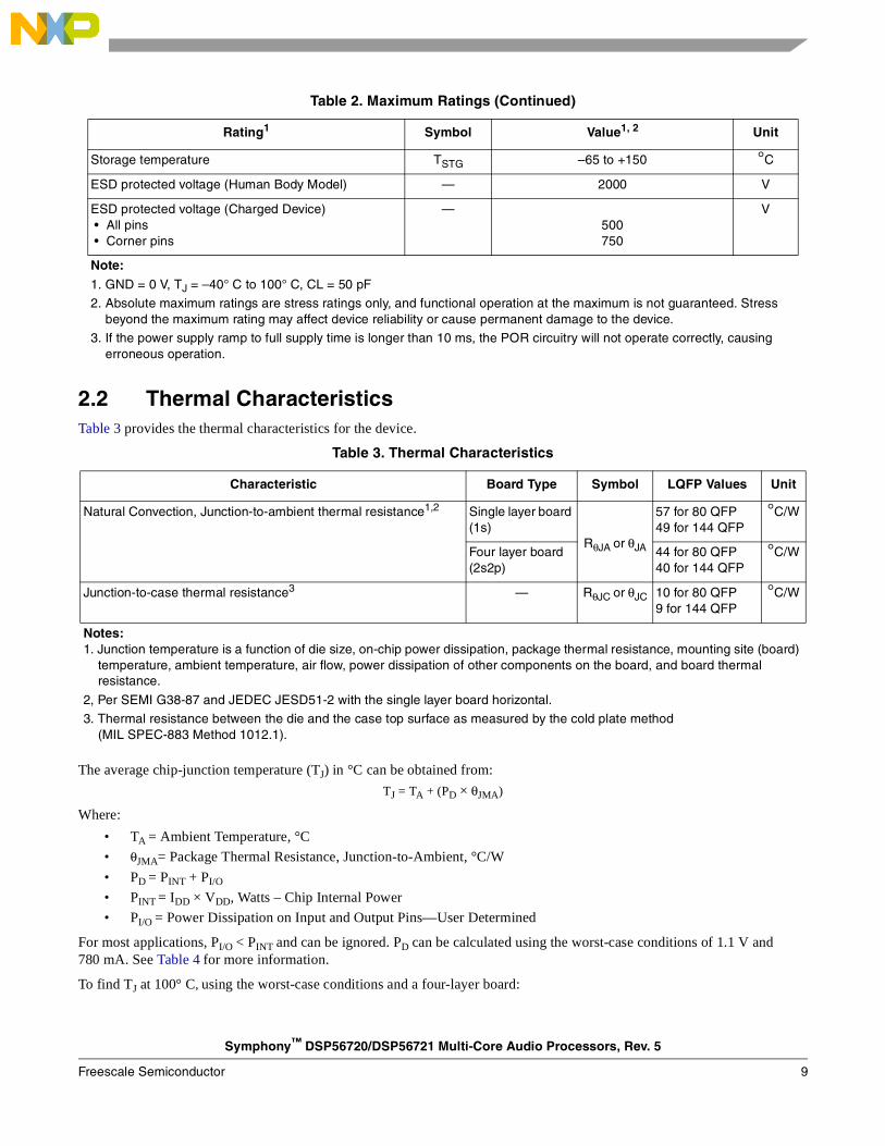
2.2 Thermal CharacteristicsTable 3 provides the thermal characteristics for the device.
The average chip-junction temperature (TJ) in °C can be obtained from:
TJ = TA + (PD × θJMA)
Where:
• TA = Ambient Temperature, °C
• θJMA= Package Thermal Resistance, Junction-to-Ambient, °C/W
• PD = PINT + PI/O
• PINT = IDD × VDD, Watts – Chip Internal Power
• PI/O = Power Dissipation on Input and Output Pins—User Determined
For most applications, PI/O < PINT and can be ignored. PD can be calculated using the worst-case conditions of 1.1 V and 780 mA. See Table 4 for more information.
To find TJ at 100° C, using the worst-case conditions and a four-layer board:
Storage temperature TSTG –65 to +150 °C
ESD protected voltage (Human Body Model) — 2000 V
ESD protected voltage (Charged Device) • All pins • Corner pins
—500750
V
Note:1. GND = 0 V, TJ = –40° C to 100° C, CL = 50 pF
2. Absolute maximum ratings are stress ratings only, and functional operation at the maximum is not guaranteed. Stress beyond the maximum rating may affect device reliability or cause permanent damage to the device.
3. If the power supply ramp to full supply time is longer than 10 ms, the POR circuitry will not operate correctly, causing erroneous operation.
Table 3. Thermal Characteristics
Characteristic Board Type Symbol LQFP Values Unit
Natural Convection, Junction-to-ambient thermal resistance1,2 Single layer board (1s)
RθJA or θJA
57 for 80 QFP49 for 144 QFP
°C/W
Four layer board (2s2p)
44 for 80 QFP40 for 144 QFP
°C/W
Junction-to-case thermal resistance3 — RθJC or θJC 10 for 80 QFP9 for 144 QFP
°C/W
Notes:1. Junction temperature is a function of die size, on-chip power dissipation, package thermal resistance, mounting site (board)
temperature, ambient temperature, air flow, power dissipation of other components on the board, and board thermal resistance.
2, Per SEMI G38-87 and JEDEC JESD51-2 with the single layer board horizontal.
3. Thermal resistance between the die and the case top surface as measured by the cold plate method (MIL SPEC-883 Method 1012.1).
Table 2. Maximum Ratings (Continued)
Rating1 Symbol Value1, 2 Unit
Symphony™ DSP56720/DSP56721 Multi-Core Audio Processors, Rev. 5
Freescale Semiconductor 9

PD = 1.1 V × 625 mA
= 0.6875 W
TJ = 70 + (0.6875 × 40)
= 97.5° C
2.3 Power RequirementsTo prevent high current conditions due to possible improper sequencing of the power supplies, use an external Schottky diode as shown in Figure 6, connected between the DSP56720/DSP56721 IO_VDD and Core_VDD power pins.
Figure 6. Prevent High Current Conditions by Using External Schottky Diode
If an external Schottky diode is not used (to prevent a high current condition at power-up), then IO_VDD must be applied ahead of Core_VDD, as shown in Figure 7.
Figure 7. Prevent High Current Conditions by Applying IO_VDD Before Core_VDD
For correct operation of the internal power-on reset logic, the Core_VDD ramp rate (Tr) to full supply must be less than 10 ms, as shown in Figure 8.
There are no power down requirement for the digital 1.0 V (CORE) and 3.3 V (IO). For the analog PLL power, the digital (IO) 3.3 V must be power up before the analog 3.3 V power. Similarly, for power down the digital (IO) 3.3 V must be power down after the analog power 3.3 V. This requirement is for avoiding possible leakage.
Figure 8. Ensure Correct Operation of Power-On Reset with Fast Ramp of Core_VDD
IO_VDD
Core_VDD
ExternalSchottky
Diode
Core_VDD
IO_VDD
Core_VDD
Tr must be < 10 ms
0 V
1.0 VTr
Symphony™ DSP56720/DSP56721 Multi-Core Audio Processors, Rev. 5
Freescale Semiconductor10
2.4 Power Consumption ConsiderationsPower dissipation is a key issue in portable DSP applications. Some of the factors which affect current consumption are described in this section. Most of the current consumed by CMOS devices is alternating current (ac), which is charging and discharging the capacitances of the pins and internal nodes.
Current consumption is described by the following formula:
Eqn. 1
where C=node/pin capacitanceV=voltage swingf=frequency of node/pin toggle
The maximum internal current (ICCImax) value reflects the typical possible switching of the internal buses on best-case operation conditions, which is not necessarily a real application case. The typical internal current (ICCItyp) value reflects the average switching of the internal buses on typical operating conditions.
For applications that require very low current consumption, do the following:
• Minimize the number of pins that are switching.
• Minimize the capacitive load on the pins.
One way to evaluate power consumption is to use a current per MIPS measurement methodology to minimize specific board effects (for example, to compensate for measured board current not caused by the DSP). Use the test algorithm, specific test current measurements, and the following equation to derive the current per MIPS value.
I/MIPS = I/MHz = (ItypF2 - ItypF1)/(F2 - F1) Eqn. 3
where : ItypF2=current at F2ItypF1=current at F1F2=high frequency (any specified operating frequency)F1=low frequency (any specified operating frequency lower than F2)
NOTEF1 should be significantly less than F2. For example, F2 could be 66 MHz and F1 could be 33 MHz. The degree of difference between F1 and F2 determines the amount of precision with which the current rating can be determined for an application.
Example 1. Power Consumption Example
For a GPIO address pin loaded with 50 pF capacitance, operating at 3.3 V, and with a 150 MHz clock, toggling at its maximum possible rate (75 MHz), the current consumption is
Eqn. 2
I C V× f×=
I 50x10 12– x3.3x75x106 12.375mA= =
Symphony™ DSP56720/DSP56721 Multi-Core Audio Processors, Rev. 5
Freescale Semiconductor 11

2.5 DC Electrical CharacteristicsTable 4 shows the DC electrical characteristics.
Table 4. DC Electrical Characteristics
Characteristics Symbol Min Typ Max Unit
Commercial Supply voltages: • Core (Core_VDD) • PLL (PLLD_VDD, PLLD1_VDD)
VDD 0.9 1 1.1 V
Supply voltages: • I/O (IO_VDD) • PLL (PLLP_VDD, PLLP1_VDD) • PLL (PLLA_VDD, PLLA1_VDD)
VDDIO 3.14 3.3 3.46 V
Automotive Supply voltages: • Core (Core_VDD) • PLL (PLLD_VDD, PLLD1_VDD)
VDD 0.95 1 1.05 V
Supply voltages: • I/O (IO_VDD) • PLL (PLLP_VDD, PLLP1_VDD) • PLL (PLLA_VDD, PLLA1_VDD)
VDDIO 3.14 3.3 3.46 V
Note: To avoid a high current condition and possible system damage, all 3.3 V supplies must rise before the 1.0 V supplies rise.
Input low voltage VIL –0.3 — 0.8 V
Input leakage current IIN — — ± 84 μA
Clock pin Input Capacitance (EXTAL) CIN — 18 — pF
High impedance (off-state) input current (@ 3.3 V or 0 V) ITSI –10 — 10 μA
Output high voltage
IOH = -12 mALSYNC_OUT, LALE, LCLK Pins IOH = -16 mA, TDO Pin IOH = -24 mA
VOH 2.4 — — V
Output low voltage
IOL = 12 mALSYNC_OUT, LALE, LCLK Pins IOL = 16 mA, TDO Pins IOL = 24 mA
VOL — — 0.4 V
Internal pull-up resistor RPU 64 92 142 kΩ
Internal pull-down resistor RPD 57 90 157 kΩ
Commercial Internal supply current1 (core only) at internal clock of 200 MHz • In Normal mode ICCI — 224 445 mA
• In Wait mode ICCW — 121 353 mA
• In Stop mode2 ICCS — 90 327 mA
Symphony™ DSP56720/DSP56721 Multi-Core Audio Processors, Rev. 5
Freescale Semiconductor12
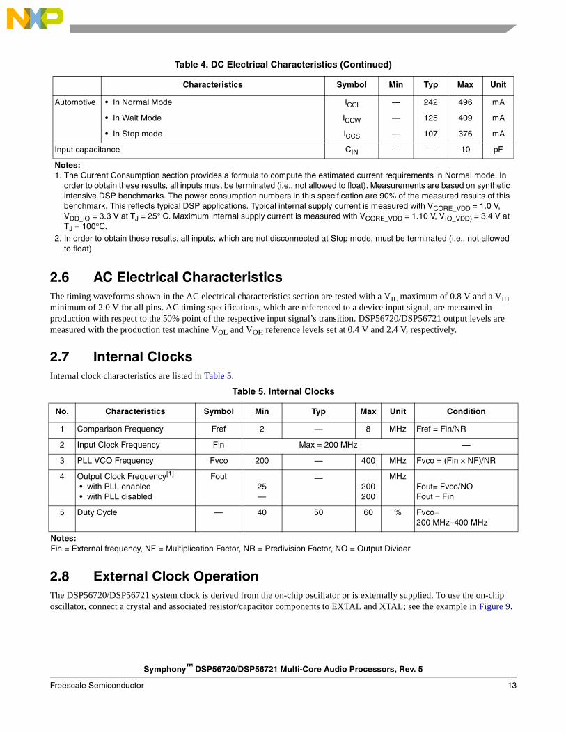
2.6 AC Electrical CharacteristicsThe timing waveforms shown in the AC electrical characteristics section are tested with a VIL maximum of 0.8 V and a VIH minimum of 2.0 V for all pins. AC timing specifications, which are referenced to a device input signal, are measured in production with respect to the 50% point of the respective input signal’s transition. DSP56720/DSP56721 output levels are measured with the production test machine VOL and VOH reference levels set at 0.4 V and 2.4 V, respectively.
2.7 Internal Clocks Internal clock characteristics are listed in Table 5.
2.8 External Clock OperationThe DSP56720/DSP56721 system clock is derived from the on-chip oscillator or is externally supplied. To use the on-chip oscillator, connect a crystal and associated resistor/capacitor components to EXTAL and XTAL; see the example in Figure 9.
Automotive • In Normal Mode ICCI — 242 496 mA
• In Wait Mode ICCW — 125 409 mA
• In Stop mode ICCS — 107 376 mA
Input capacitance CIN — — 10 pF
Notes:1. The Current Consumption section provides a formula to compute the estimated current requirements in Normal mode. In
order to obtain these results, all inputs must be terminated (i.e., not allowed to float). Measurements are based on synthetic intensive DSP benchmarks. The power consumption numbers in this specification are 90% of the measured results of this benchmark. This reflects typical DSP applications. Typical internal supply current is measured with VCORE_VDD = 1.0 V, VDD_IO = 3.3 V at TJ = 25° C. Maximum internal supply current is measured with VCORE_VDD = 1.10 V, VIO_VDD) = 3.4 V at TJ = 100°C.
2. In order to obtain these results, all inputs, which are not disconnected at Stop mode, must be terminated (i.e., not allowed to float).
Table 5. Internal Clocks
No. Characteristics Symbol Min Typ Max Unit Condition
1 Comparison Frequency Fref 2 — 8 MHz Fref = Fin/NR
2 Input Clock Frequency Fin Max = 200 MHz —
3 PLL VCO Frequency Fvco 200 — 400 MHz Fvco = (Fin × NF)/NR
4 Output Clock Frequency[1]
• with PLL enabled • with PLL disabled
Fout25—
—200200
MHzFout= Fvco/NOFout = Fin
5 Duty Cycle — 40 50 60 % Fvco= 200 MHz–400 MHz
Notes:Fin = External frequency, NF = Multiplication Factor, NR = Predivision Factor, NO = Output Divider
Table 4. DC Electrical Characteristics (Continued)
Characteristics Symbol Min Typ Max Unit
Symphony™ DSP56720/DSP56721 Multi-Core Audio Processors, Rev. 5
Freescale Semiconductor 13

Figure 9. Using the On-Chip Oscillator
If the DSP56720/DSP56721 system clock is an externally supplied square wave voltage source, it is connected to EXTAL (Figure 10). When the external square wave source is connected to EXTAL, the XTAL pin is not used.
Figure 10. External Clock Timing
Table 6 lists the clock operation.
Table 6. Clock Operation
No. Characteristics Symbol Min Max Units
1 EXTAL input high 1
(40% to 60% duty cycle) • Crystal oscillator • Square wave input
Eth 16.672.5
100inf
ns
2 EXTAL input low1
(40% to 60% duty cycle) • Crystal oscillator • Square wave input
Etl 16.672.5
100inf
ns
3 EXTAL cycle time • With PLL disabled • With PLL enabled
Etc 533.3
inf500
ns
4 Instruction cycle time • With PLL disabled • With PLL enabled
Tc 5.005.00
inf5120
ns
Notes:1. Measured at 50% of the input transition.
2. The indicated duty cycle is for the specified maximum frequency for which a part is rated. The minimum clock high or low time required for correct operation, however, remains the same at lower operating frequencies; therefore, when a lower clock frequency is used, the signal symmetry may vary from the specified duty cycle as long as the minimum high time and low time requirements are met.
XTALEXTAL Suggested component values:
Fosc = 24.576 MHzR = 1 M ±10%C (EXTAL)= 18 pF
Calculations are for a 5 – 30 MHz crystal with the following parameters:• Shunt capacitance (C0) of 10 pF – 12 pF• Series resistance 40 Ohm
C (XTAL) = 18 pF
• Drive level of 10 μW
R
XTAL1CC
EXTAL
VIL
VIHMidpoint
Note: The midpoint is 0.5 (VIH + VIL).
ETH ETL
ETC
2
3
1
Symphony™ DSP56720/DSP56721 Multi-Core Audio Processors, Rev. 5
Freescale Semiconductor14

2.9 Reset, Stop, Mode Select, and Interrupt TimingTable 7 shows the reset, stop, mode select, and interrupt timing.
Table 7. Reset, Stop, Mode Select, and Interrupt Timing Parameters
No. Characteristics Expression Min Max Unit
10 Delay from RESET assertion to all pins at reset value3 — — 11 ns
11 Required RESET duration4
• Power on, external clock generator, PLL disabled • Power on, external clock generator, PLL enabled
2 × TC2 × TC
1010
——
nsns
13 Syn reset deassert delay time • Minimum 2 × TC 10 — ns
• Maximum (PLL enabled) (2 x TC) + TLOCK 200 — us
14 Mode select setup time — 10.0 — ns
15 Mode select hold time — 12 — ns
16 Minimum edge-triggered interrupt request assertion width — 7 — ns
17 Minimum edge-triggered interrupt request deassertion width — 4 — ns
18 Delay from interrupt trigger to interrupt code execution 10 × TC + 4 54 — ns
19 Duration of level sensitive IRQA assertion to ensure interrupt service (when exiting Stop)1, 2, 3
• PLL is active during Stop and Stop delay is enabled (OMR Bit 6 = 0) (128 Kbytes × TC) 655 — μs
• PLL is active during Stop and Stop delay is not enabled (OMR Bit 6 = 1)
25 × TC 125 — ns
• PLL is not active during Stop and Stop delay is enabled (OMR Bit 6 = 0)
(128 Kbytes × TC) + TLOCK
855 — μs
• PLL is not active during Stop and Stop delay is not enabled (OMR Bit 6 = 1)
(25 × TC) + TLOCK 200 — μs
20 • Delay from IRQA, IRQB, IRQC, IRQD, NMI assertion to general-purpose transfer output valid caused by first interrupt instruction execution1
10 × TC + 3.8 — 53.8 ns
21 Interrupt Requests Rate1
• ESAI, ESAI_1, ESAI_2, ESAI_3, SHI, SHI_1, Timer, Timer_1 12 × TC — 60.0 ns
• DMA 8 × TC — 40.0 ns
• IRQ, NMI (edge trigger) 8 × TC — 40.0 ns
• IRQ (level trigger) 12 × TC — 60.0 ns
Symphony™ DSP56720/DSP56721 Multi-Core Audio Processors, Rev. 5
Freescale Semiconductor 15
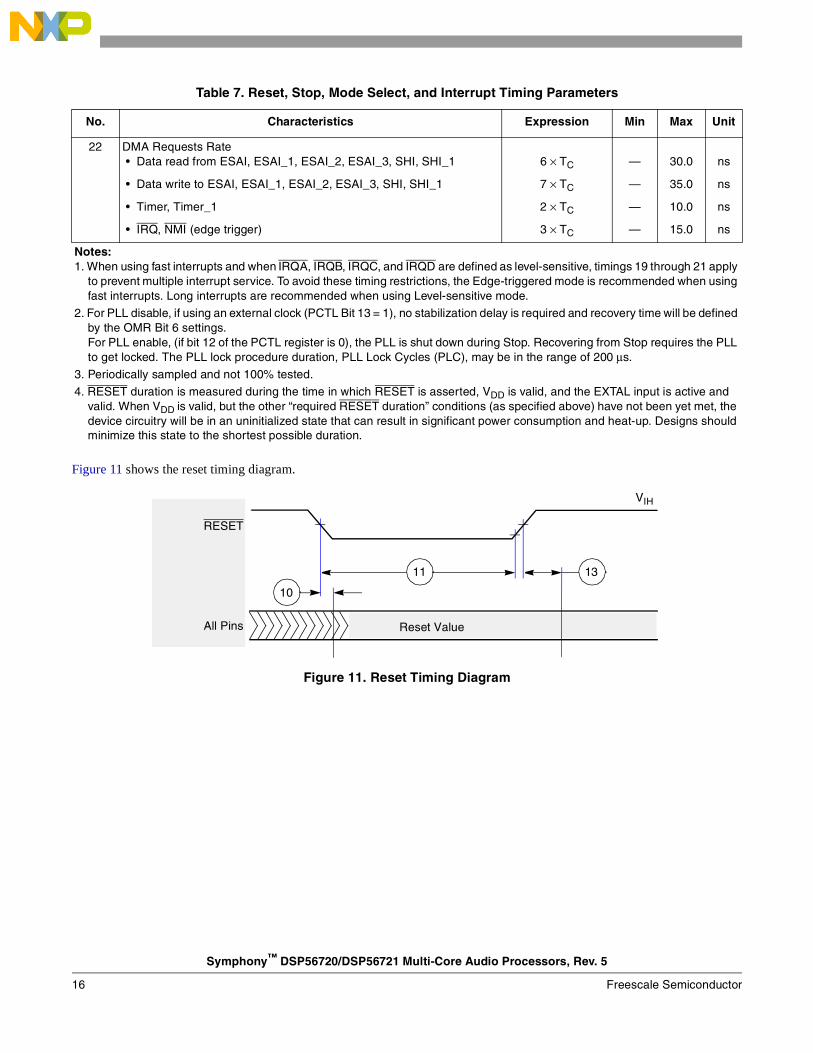
Figure 11 shows the reset timing diagram.
Figure 11. Reset Timing Diagram
22 DMA Requests Rate • Data read from ESAI, ESAI_1, ESAI_2, ESAI_3, SHI, SHI_1 6 × TC — 30.0 ns
• Data write to ESAI, ESAI_1, ESAI_2, ESAI_3, SHI, SHI_1 7 × TC — 35.0 ns
• Timer, Timer_1 2 × TC — 10.0 ns
• IRQ, NMI (edge trigger) 3 × TC — 15.0 ns
Notes:1. When using fast interrupts and when IRQA, IRQB, IRQC, and IRQD are defined as level-sensitive, timings 19 through 21 apply
to prevent multiple interrupt service. To avoid these timing restrictions, the Edge-triggered mode is recommended when using fast interrupts. Long interrupts are recommended when using Level-sensitive mode.
2. For PLL disable, if using an external clock (PCTL Bit 13 = 1), no stabilization delay is required and recovery time will be defined by the OMR Bit 6 settings.For PLL enable, (if bit 12 of the PCTL register is 0), the PLL is shut down during Stop. Recovering from Stop requires the PLL to get locked. The PLL lock procedure duration, PLL Lock Cycles (PLC), may be in the range of 200 μs.
3. Periodically sampled and not 100% tested.
4. RESET duration is measured during the time in which RESET is asserted, VDD is valid, and the EXTAL input is active and valid. When VDD is valid, but the other “required RESET duration” conditions (as specified above) have not been yet met, the device circuitry will be in an uninitialized state that can result in significant power consumption and heat-up. Designs should minimize this state to the shortest possible duration.
Table 7. Reset, Stop, Mode Select, and Interrupt Timing Parameters
No. Characteristics Expression Min Max Unit
VIH
RESET
All Pins
10
11 13
Reset Value
Symphony™ DSP56720/DSP56721 Multi-Core Audio Processors, Rev. 5
Freescale Semiconductor16

Figure 12 shows the external fast interrupt timing diagram.
Figure 12. External Fast Interrupt Timing Diagram
Figure 13 shows the negative edge-triggered external interrupt timing diagram.
Figure 13. External Interrupt Timing Diagram (Negative Edge-Triggered)
a) First Interrupt Instruction Execution
GeneralPurpose
I/O
IRQA, IRQB,IRQC, IRQD,
NMI,NMI_1
b) General Purpose I/O
IRQA, IRQB,IRQC, IRQD,
NMI,NMI_1
1819
20
IRQA, IRQB,IRQC, IRQD,
NMI,NMI_1
IRQA, IRQB,IRQC, IRQD,
NMI,NMI_1
16
17
Symphony™ DSP56720/DSP56721 Multi-Core Audio Processors, Rev. 5
Freescale Semiconductor 17
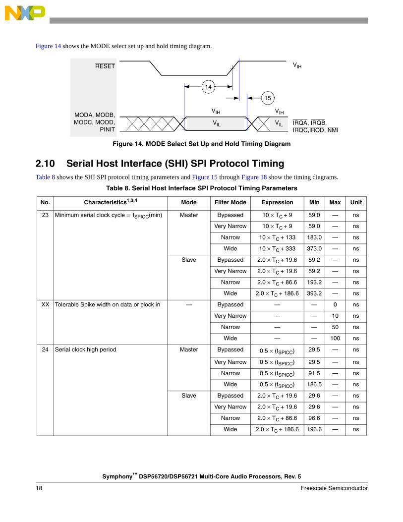
Figure 14 shows the MODE select set up and hold timing diagram.
Figure 14. MODE Select Set Up and Hold Timing Diagram
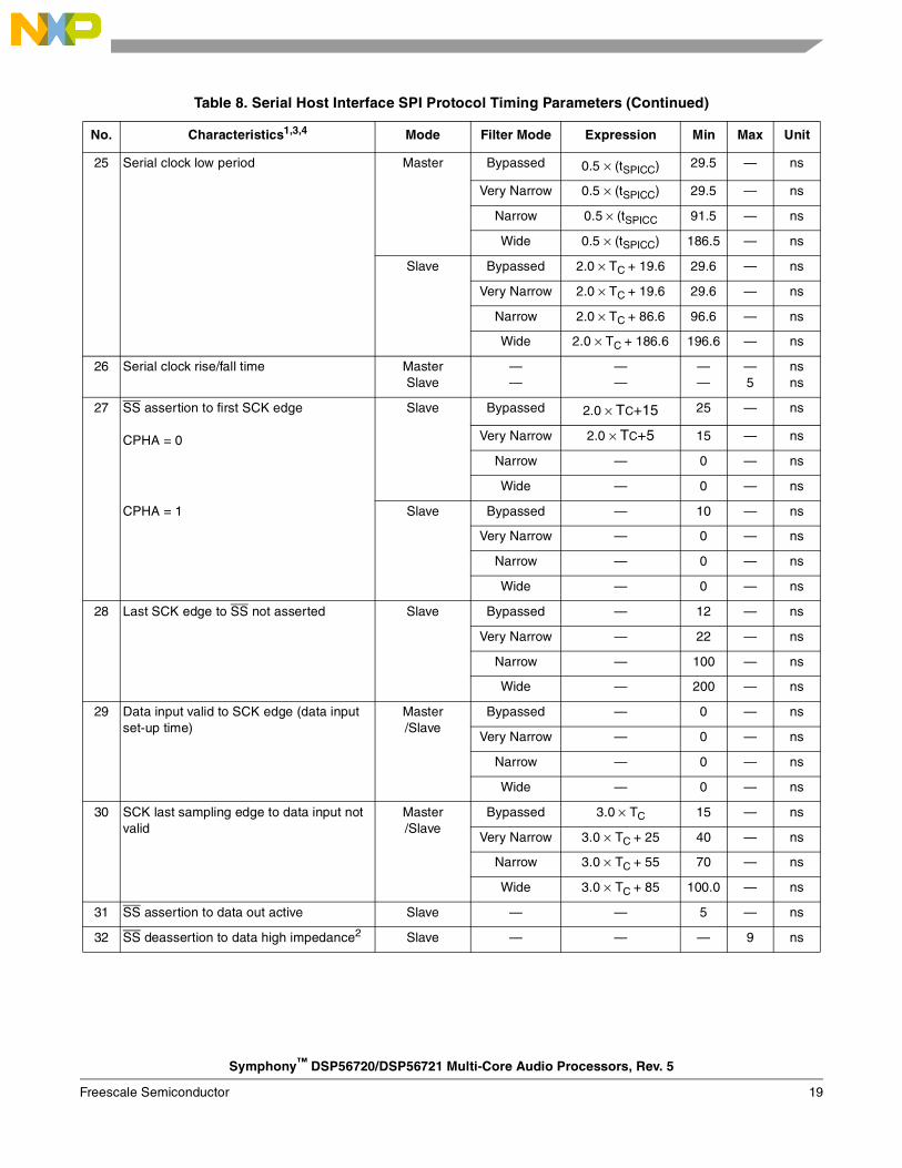
2.10 Serial Host Interface (SHI) SPI Protocol TimingTable 8 shows the SHI SPI protocol timing parameters and Figure 15 through Figure 18 show the timing diagrams.
Table 8. Serial Host Interface SPI Protocol Timing Parameters
No. Characteristics1,3,4 Mode Filter Mode Expression Min Max Unit
23 Minimum serial clock cycle = tSPICC(min) Master Bypassed 10 × TC + 9 59.0 — ns
Very Narrow 10 × TC + 9 59.0 — ns
Narrow 10 × TC + 133 183.0 — ns
Wide 10 × TC + 333 373.0 — ns
Slave Bypassed 2.0 × TC + 19.6 59.2 — ns
Very Narrow 2.0 × TC + 19.6 59.2 — ns
Narrow 2.0 × TC + 86.6 193.2 — ns
Wide 2.0 × TC + 186.6 393.2 — ns
XX Tolerable Spike width on data or clock in — Bypassed — — 0 ns
Very Narrow — — 10 ns
Narrow — — 50 ns
Wide — — 100 ns
24 Serial clock high period Master Bypassed 0.5 × (tSPICC) 29.5 — ns
Very Narrow 0.5 × (tSPICC) 29.5 — ns
Narrow 0.5 × (tSPICC) 91.5 — ns
Wide 0.5 × (tSPICC) 186.5 — ns
Slave Bypassed 2.0 × TC + 19.6 29.6 — ns
Very Narrow 2.0 × TC + 19.6 29.6 — ns
Narrow 2.0 × TC + 86.6 96.6 — ns
Wide 2.0 × TC + 186.6 196.6 — ns
RESET
MODA, MODB,MODC, MODD,
PINIT
VIH
IRQA, IRQB, IRQC,IRQD, NMI
VIH VIH
14
15
VIL VIL
Symphony™ DSP56720/DSP56721 Multi-Core Audio Processors, Rev. 5
Freescale Semiconductor18
25 Serial clock low period Master Bypassed 0.5 × (tSPICC) 29.5 — ns
Very Narrow 0.5 × (tSPICC) 29.5 — ns
Narrow 0.5 × (tSPICC 91.5 — ns
Wide 0.5 × (tSPICC) 186.5 — ns
Slave Bypassed 2.0 × TC + 19.6 29.6 — ns
Very Narrow 2.0 × TC + 19.6 29.6 — ns
Narrow 2.0 × TC + 86.6 96.6 — ns
Wide 2.0 × TC + 186.6 196.6 — ns
26 Serial clock rise/fall time MasterSlave
——
——
——
—5
nsns
27 SS assertion to first SCK edge
CPHA = 0
Slave Bypassed 2.0 × TC+15 25 — ns
Very Narrow 2.0 × TC+5 15 — ns
Narrow — 0 — ns
Wide — 0 — ns
CPHA = 1 Slave Bypassed — 10 — ns
Very Narrow — 0 — ns
Narrow — 0 — ns
Wide — 0 — ns
28 Last SCK edge to SS not asserted Slave Bypassed — 12 — ns
Very Narrow — 22 — ns
Narrow — 100 — ns
Wide — 200 — ns
29 Data input valid to SCK edge (data input set-up time)
Master/Slave
Bypassed — 0 — ns
Very Narrow — 0 — ns
Narrow — 0 — ns
Wide — 0 — ns
30 SCK last sampling edge to data input not valid
Master/Slave
Bypassed 3.0 × TC 15 — ns
Very Narrow 3.0 × TC + 25 40 — ns
Narrow 3.0 × TC + 55 70 — ns
Wide 3.0 × TC + 85 100.0 — ns
31 SS assertion to data out active Slave — — 5 — ns
32 SS deassertion to data high impedance2 Slave — — — 9 ns
Table 8. Serial Host Interface SPI Protocol Timing Parameters (Continued)
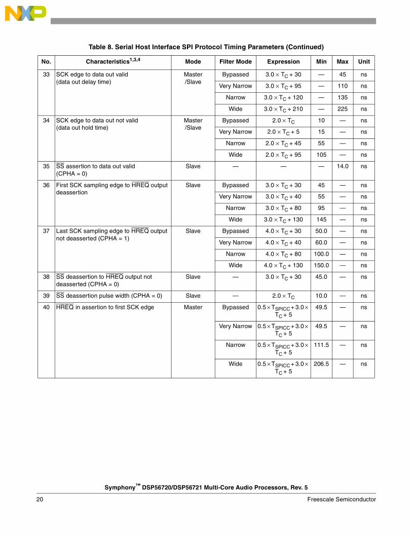
No. Characteristics1,3,4 Mode Filter Mode Expression Min Max Unit
Symphony™ DSP56720/DSP56721 Multi-Core Audio Processors, Rev. 5
Freescale Semiconductor 19
33 SCK edge to data out valid (data out delay time)
Master/Slave
Bypassed 3.0 × TC + 30 — 45 ns
Very Narrow 3.0 × TC + 95 — 110 ns
Narrow 3.0 × TC + 120 — 135 ns
Wide 3.0 × TC + 210 — 225 ns
34 SCK edge to data out not valid (data out hold time)
Master/Slave
Bypassed 2.0 × TC 10 — ns
Very Narrow 2.0 × TC + 5 15 — ns
Narrow 2.0 × TC + 45 55 — ns
Wide 2.0 × TC + 95 105 — ns
35 SS assertion to data out valid (CPHA = 0)
Slave — — — 14.0 ns
36 First SCK sampling edge to HREQ output deassertion
Slave Bypassed 3.0 × TC + 30 45 — ns
Very Narrow 3.0 × TC + 40 55 — ns
Narrow 3.0 × TC + 80 95 — ns
Wide 3.0 × TC + 130 145 — ns
37 Last SCK sampling edge to HREQ output not deasserted (CPHA = 1)
Slave Bypassed 4.0 × TC + 30 50.0 — ns
Very Narrow 4.0 × TC + 40 60.0 — ns
Narrow 4.0 × TC + 80 100.0 — ns
Wide 4.0 × TC + 130 150.0 — ns
38 SS deassertion to HREQ output not deasserted (CPHA = 0)
Slave — 3.0 × TC + 30 45.0 — ns
39 SS deassertion pulse width (CPHA = 0) Slave — 2.0 × TC 10.0 — ns
40 HREQ in assertion to first SCK edge Master Bypassed 0.5 × TSPICC + 3.0 × TC + 5
49.5 — ns
Very Narrow 0.5 × TSPICC + 3.0 × TC + 5
49.5 — ns
Narrow 0.5 × TSPICC + 3.0 × TC + 5
111.5 — ns
Wide 0.5 × TSPICC + 3.0 × TC + 5
206.5 — ns
Table 8. Serial Host Interface SPI Protocol Timing Parameters (Continued)
No. Characteristics1,3,4 Mode Filter Mode Expression Min Max Unit
Symphony™ DSP56720/DSP56721 Multi-Core Audio Processors, Rev. 5
Freescale Semiconductor20
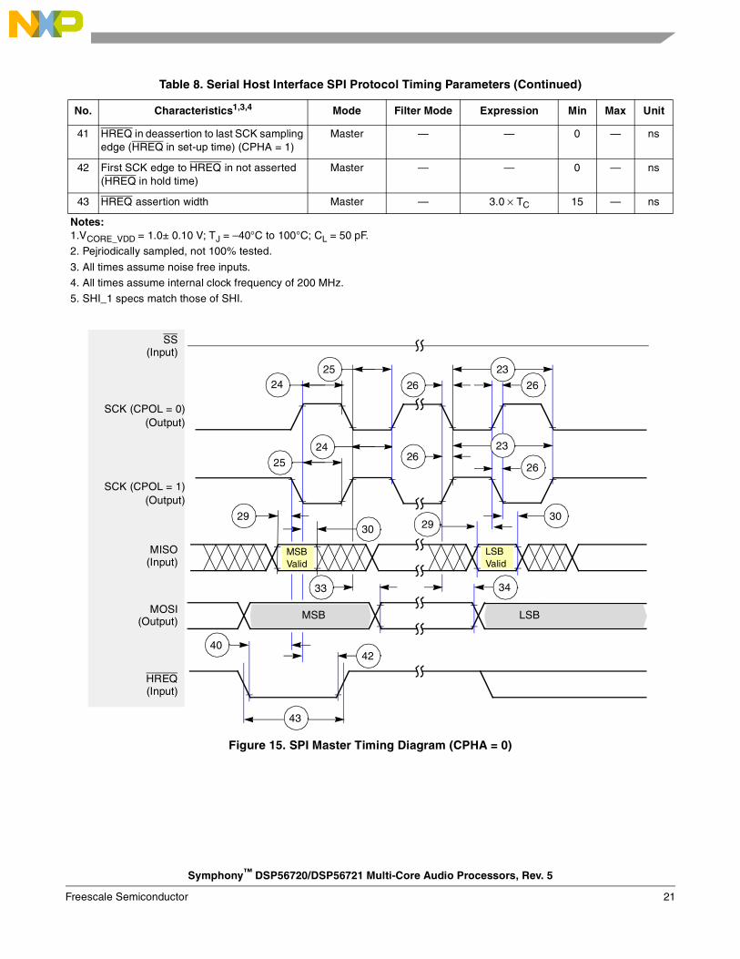
Figure 15. SPI Master Timing Diagram (CPHA = 0)
41 HREQ in deassertion to last SCK sampling edge (HREQ in set-up time) (CPHA = 1)
Master — — 0 — ns
42 First SCK edge to HREQ in not asserted (HREQ in hold time)
Master — — 0 — ns
43 HREQ assertion width Master — 3.0 × TC 15 — ns
Notes:1.VCORE_VDD = 1.0± 0.10 V; TJ = –40°C to 100°C; CL = 50 pF.
2. Pejriodically sampled, not 100% tested.
3. All times assume noise free inputs.
4. All times assume internal clock frequency of 200 MHz.
5. SHI_1 specs match those of SHI.
Table 8. Serial Host Interface SPI Protocol Timing Parameters (Continued)
No. Characteristics1,3,4 Mode Filter Mode Expression Min Max Unit
SS(Input)
SCK (CPOL = 0)(Output)
SCK (CPOL = 1)(Output)
MISO(Input)
MOSI(Output)
HREQ(Input)
2324
25
26 26
23
262625
24
2930
3029
33 34
4240
43
MSB LSB
LSB Valid
MSB Valid
Symphony™ DSP56720/DSP56721 Multi-Core Audio Processors, Rev. 5
Freescale Semiconductor 21

Figure 16. SPI Master Timing Diagram (CPHA = 1)
SS(Input)
SCK (CPOL = 0)(Output)
SCK (CPOL = 1)(Output)
MISO(Input)
MOSI(Output)
HREQ(Input)
23
24
25
26 26
23
262625
24
29 29
30
33 34
42
40 41
30
43
MSB LSB
MSB Valid
LSB Valid
Symphony™ DSP56720/DSP56721 Multi-Core Audio Processors, Rev. 5
Freescale Semiconductor22
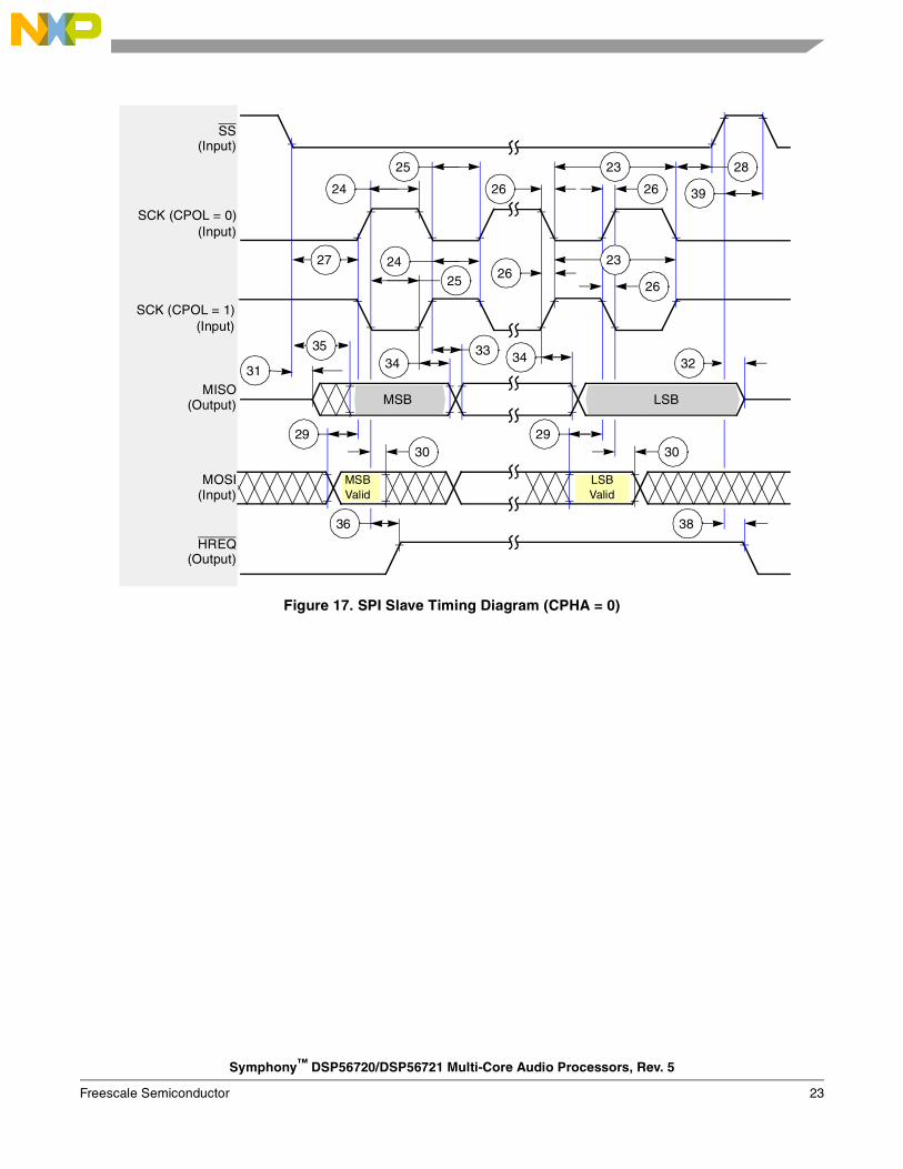
Figure 17. SPI Slave Timing Diagram (CPHA = 0)
SS(Input)
SCK (CPOL = 0)(Input)
SCK (CPOL = 1)(Input)
MISO(Output)
MOSI(Input)
HREQ(Output)
23
24
25
26 26
23
262625
24
35
31
3334
2930
3836
34 32
2930
28
39
27
LSBMSB
MSB Valid
LSB Valid
Symphony™ DSP56720/DSP56721 Multi-Core Audio Processors, Rev. 5
Freescale Semiconductor 23

Figure 18. SPI Slave Timing Diagram (CPHA = 1)
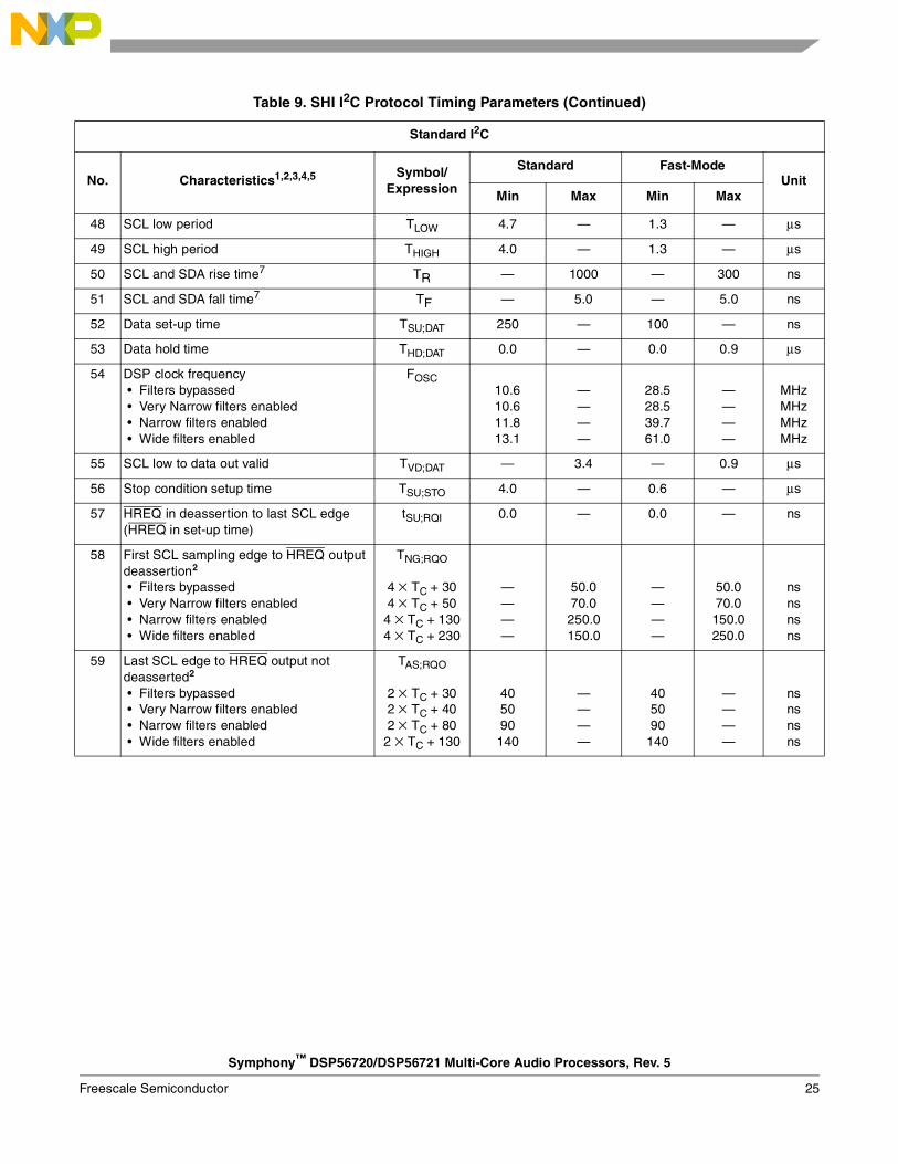
2.11 Serial Host Interface (SHI) I2C Protocol TimingTable 9 lists the SHI I2C protocol timing parameters and Figure 19 shows the timing diagram.
Table 9. SHI I2C Protocol Timing Parameters
Standard I2C
No. Characteristics1,2,3,4,5 Symbol/Expression
Standard Fast-ModeUnit
Min Max Min Max
Tolerable Spike Width on SCL or SDAFilters BypassedVery Narrow Filters enabledNarrow Filters enabledWide Filters enabled.
—————
01050
100
————
01050
100
nsnsnsns
44 SCL clock frequency FSCL — 100 — 400 kHz
44 SCL clock cycle TSCL 10 — 2.5 — μs
45 Bus free time TBUF 4.7 — 1.3 — μs
46 Start condition set-up time TSUSTA 4.7 — 0.6 — μs
47 Start condition hold time THD;STA 4.0 — 0.6 — μs
SS(Input)
SCK (CPOL = 0)(Input)
SCK (CPOL = 1)(Input)
MISO(Output)
MOSI(Input)
HREQ(Output)
23
24
25
26 26
262625
24
31
33
2930
37
34 32
29
28
27
33
30
36
MSB LSB
MSB Valid
LSB Valid
Symphony™ DSP56720/DSP56721 Multi-Core Audio Processors, Rev. 5
Freescale Semiconductor24
48 SCL low period TLOW 4.7 — 1.3 — μs
49 SCL high period THIGH 4.0 — 1.3 — μs
50 SCL and SDA rise time7 TR — 1000 — 300 ns
51 SCL and SDA fall time7 TF — 5.0 — 5.0 ns
52 Data set-up time TSU;DAT 250 — 100 — ns
53 Data hold time THD;DAT 0.0 — 0.0 0.9 μs
54 DSP clock frequency • Filters bypassed • Very Narrow filters enabled • Narrow filters enabled • Wide filters enabled
FOSC10.610.611.813.1
————
28.528.539.761.0
————
MHzMHzMHzMHz
55 SCL low to data out valid TVD;DAT — 3.4 — 0.9 μs
56 Stop condition setup time TSU;STO 4.0 — 0.6 — μs
57 HREQ in deassertion to last SCL edge (HREQ in set-up time)
tSU;RQI 0.0 — 0.0 — ns
58 First SCL sampling edge to HREQ output deassertion2
• Filters bypassed • Very Narrow filters enabled • Narrow filters enabled • Wide filters enabled
TNG;RQO
4 × TC + 304 × TC + 50
4 × TC + 1304 × TC + 230
————
50.070.0250.0150.0
————
50.070.0150.0250.0
nsnsnsns
59 Last SCL edge to HREQ output not deasserted2
• Filters bypassed • Very Narrow filters enabled • Narrow filters enabled • Wide filters enabled
TAS;RQO
2 × TC + 302 × TC + 402 × TC + 80
2 × TC + 130
405090140
————
405090
140
————
nsnsnsns
Table 9. SHI I2C Protocol Timing Parameters (Continued)
Standard I2C
No. Characteristics1,2,3,4,5 Symbol/Expression
Standard Fast-ModeUnit
Min Max Min Max
Symphony™ DSP56720/DSP56721 Multi-Core Audio Processors, Rev. 5
Freescale Semiconductor 25
2.12 Programming the SHI I2C Serial ClockThe programmed serial clock cycle, TI
2CCP, is specified by the value of the HDM[7:0] and HRS bits of the HCKR (SHI clock
control register).
The expression for TI2CCP is
TI2CCP = [TC × 2 × (HDM[7:0] + 1) × (7 × (1 — HRS) + 1)] Eqn. 4
where
— HRS is the pre scaler rate select bit. When HRS is cleared, the fixed divide-by-eight pre scaler is operational. When HRS is set, the pre scaler is bypassed.
— HDM[7:0] are the divider modulus select bits. A divide ratio from 1 to 256 (HDM[7:0] = $00 to $FF) may be selected.
In I2C mode, the user may select a value for the programmed serial clock cycle from
6 × TC (if HDM[7:0] = $02 and HRS = 1) Eqn. 5
to
4096 × TC (if HDM[7:0] = $FF and HRS = 0) Eqn. 6
The programmed serial clock cycle (TI2CCP) should be chosen in order to achieve the desired SCL serial clock cycle (TSCL), as
shown in Equation 4.
TI2CCP + 3 × TC + 45ns + TR (Nominal, SCL Serial Clock Cycle (TSCL) generated as master) Eqn. 7
60 HREQ in assertion to first SCL edge • Filters bypassed • Very Narrow filters enabled • Narrow filters enabled • Wide filters enabled
TAS;RQI4327431742824227
————
927917877827
————
nsnsnsns
61 First SCL edge to HREQ is not asserted(HREQ in hold time.)
tHO;RQI 0.0 — 0.0 — ns
Notes:1. VCORE_VDD = 1.00± 0.10 V; TJ = –40°C to 100°C; CL = 50 pF.
2. Pull-up resistor: R P (min) = 1.5kΩ.
3. Capacitive load: C b (max) = 50 pF.
4. All times assume noise free inputs.
5. All times assume internal clock frequency of 200 MHz.
6. SHI_1 specs match those of SHI.
7. Master Mode
Table 9. SHI I2C Protocol Timing Parameters (Continued)
Standard I2C
No. Characteristics1,2,3,4,5 Symbol/Expression
Standard Fast-ModeUnit
Min Max Min Max
Symphony™ DSP56720/DSP56721 Multi-Core Audio Processors, Rev. 5
Freescale Semiconductor26

Figure 19. I2C Timing Diagram
2.13 Enhanced Serial Audio Interface (ESAI) TimingTable 10 lists the ESAI timing parameters and Figure 20 through Figure 23 show the timing diagrams.
Table 10. Enhanced Serial Audio Interface Timing Parameters
No. Characteristics1, 3, 4 Symbol Expression5 Min Max Condition2 Unit
62 Clock cycle5 tSSICC 4 × Tc4 × Tc
20.020.0
——
i cki ck
ns
63 Clock high period • For internal clock — 2 × Tc 10 — —
ns
• For external clock — 2 × Tc 10 — —
64 Clock low period • For internal clock — 2 × Tc 10 — —
ns
• For external clock — 2 × Tc 10 — —
65 SCKR rising edge to FSR out (bl) high — — ——
17.07.0
x cki ck a
ns
66 SCKR rising edge to FSR out (bl) low — — ——
17.07.0
x cki ck a
ns
67 SCKR rising edge to FSR out (wr) high6 — — ——
19.09.0
x cki ck a
ns
68 SCKR rising edge to FSR out (wr) low6 — — ——
19.09.0
x cki ck a
ns
69 SCKR rising edge to FSR out (wl) high — — ——
16.06.0
x cki ck a
ns
70 SCKR rising edge to FSR out (wl) low — — ——
17.07.0
x cki ck a
ns
44
46 49 48
5051 53
5245
58 55 56
61
47
6057
59
SCL
SDA
HREQ
Stop Start MSB LSB ACK Stop
Symphony™ DSP56720/DSP56721 Multi-Core Audio Processors, Rev. 5
Freescale Semiconductor 27

71 Data in setup time before SCKR (SCK in synchronous mode) falling edge
— — 519.0
——
x cki ck
ns
72 Data in hold time after SCKR falling edge — — 3.59.0
——
x cki ck
ns
73 FSR input (bl, wr) high before SCKR falling edge 6 — — 2.012.0
——
x cki ck a
ns
74 FSR input (wl) high before SCKR falling edge — — 2.012.0
——
x cki ck a
ns
75 FSR input hold time after SCKR falling edge — — 2.58.5
——
x cki ck a
ns
76 Flags input setup before SCKR falling edge — — 0.019.0
——
x cki ck s
ns
77 Flags input hold time after SCKR falling edge — — 6.00.0
——
x cki ck s
ns
78 SCKT rising edge to FST out (bl) high — — ——
148.0
x cki ck
ns
79 SCKT rising edge to FST out (bl) low — — ——
20.010.0
x cki ck
ns
80 SCKT rising edge to FST out (wr) high6 — — ——
20.010.0
x cki ck
ns
81 SCKT rising edge to FST out (wr) low6 — — ——
22.012.0
x cki ck
ns
82 SCKT rising edge to FST out (wl) high — — ——
149.0
x cki ck
ns
83 SCKT rising edge to FST out (wl) low — — ——
1410.0
x cki ck
ns
84 SCKT rising edge to data out enable from high impedance
— — ——
22.017.0
x cki ck
ns
85 SCKT rising edge to transmitter #0 drive enable assertion
— — ——
17.011.0
x cki ck
ns
86 SCKT rising edge to data out valid — — ——
1313.0
x cki ck
ns
87 SCKT rising edge to data out high impedance7 — — ——
1316.0
x cki ck
ns
88 SCKT rising edge to transmitter #0 drive enable deassertion7
— — ——
14.09.0
x cki ck
ns
89 FST input (bl, wr) setup time before SCKT falling edge6 — — 2.018.0
——
x cki ck
ns
90 FST input (wl) setup time before SCKT falling edge — — 2.018.0
——
x cki ck
ns
91 FST input hold time after SCKT falling edge — — 4.05.0
——
x cki ck
ns
Table 10. Enhanced Serial Audio Interface Timing Parameters (Continued)
No. Characteristics1, 3, 4 Symbol Expression5 Min Max Condition2 Unit
Symphony™ DSP56720/DSP56721 Multi-Core Audio Processors, Rev. 5
Freescale Semiconductor28

92 FST input (wl) to data out enable from high impedance — — — 21.0 — ns
93 FST input (wl) to transmitter #0 drive enable assertion — — — 14.0 — ns
94 Flag output valid after SCKT rising edge — — ——
14.09.0
x cki ck
ns
95 HCKR/HCKT clock cycle — 2 × TC 10 — — ns
96 HCKT input rising edge to SCKT output — — — 18.0 — ns
97 HCKR input rising edge to SCKR output — — — 18.0 — ns
Notes:1. VCORE_VDD = 1.00 ± 0.10 V; TJ = –40°C to 100°C; CL = 50 pF.
2. i ck = internal clockx ck = external clocki ck a = internal clock, asynchronous mode (Asynchronous implies that SCKT and SCKR are two different clocks.)i ck s = internal clock, synchronous mode (Synchronous implies that SCKT and SCKR are the same clock.)
3. bl = bit lengthwl = word lengthwr = word length relative
4. SCKT(SCKT pin) = transmit clockSCKR(SCKR pin) = receive clockFST(FST pin) = transmit frame syncFSR(FSR pin) = receive frame syncHCKT(HCKT pin) = transmit high frequency clockHCKR(HCKR pin) = receive high frequency clock
5. For the internal clock, the external clock cycle is defined by Tc and the ESAI control register.
6. The word-relative frame sync signal waveform relative to the clock operates in the same manner as the bit-length frame sync signal waveform, but spreads from one serial clock before first bit clock (same as bit length frame sync signal), until the one before last bit clock of the first word in frame.
7. Periodically sampled and not 100% tested.
8. ESAI_1, ESAI_2, ESAI_3 specs match those of ESAI.
Table 10. Enhanced Serial Audio Interface Timing Parameters (Continued)
No. Characteristics1, 3, 4 Symbol Expression5 Min Max Condition2 Unit
Symphony™ DSP56720/DSP56721 Multi-Core Audio Processors, Rev. 5
Freescale Semiconductor 29
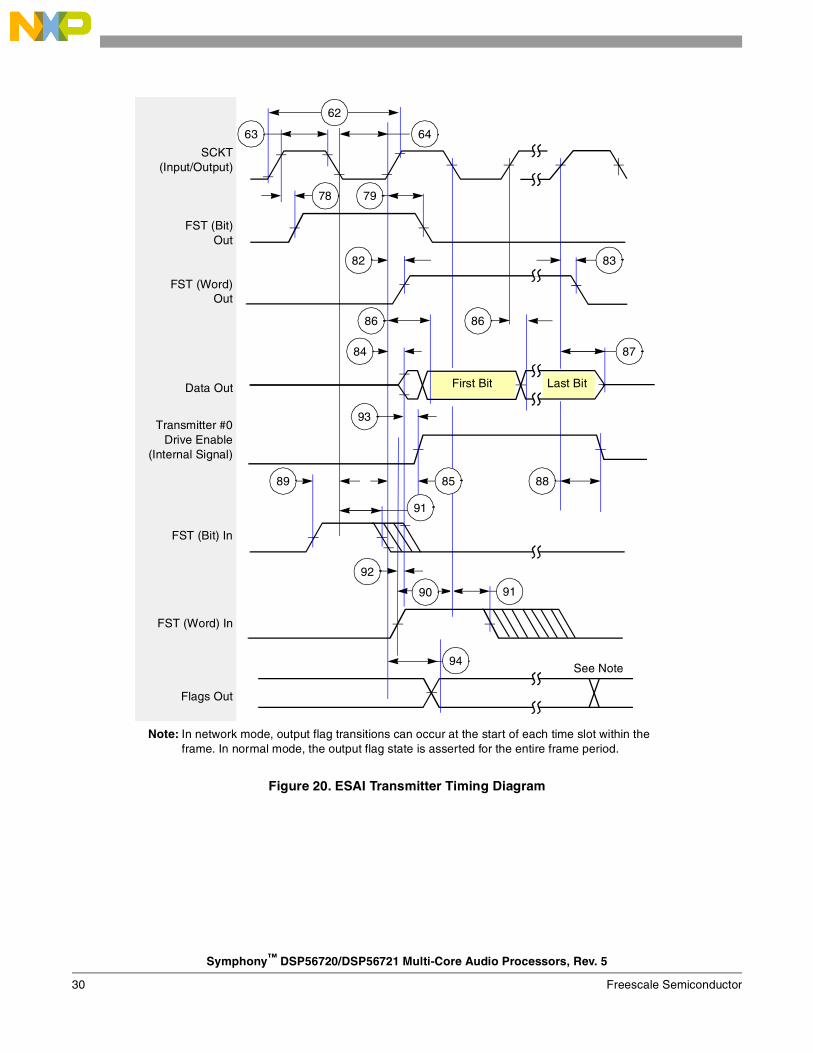
Figure 20. ESAI Transmitter Timing Diagram
See Note
SCKT(Input/Output)
FST (Bit)Out
FST (Word)Out
Data Out
Transmitter #0Drive Enable
(Internal Signal)
FST (Bit) In
FST (Word) In
Flags Out
Note: In network mode, output flag transitions can occur at the start of each time slot within the frame. In normal mode, the output flag state is asserted for the entire frame period.
62
64
78 79
82 83
87
8686
84
93
8885
91
89
92
90 91
94
63
Last BitFirst Bit
Symphony™ DSP56720/DSP56721 Multi-Core Audio Processors, Rev. 5
Freescale Semiconductor30
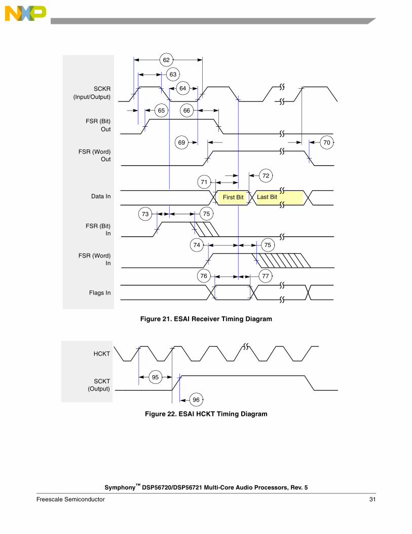
Figure 21. ESAI Receiver Timing Diagram
Figure 22. ESAI HCKT Timing Diagram
SCKR(Input/Output)
FSR (Bit)Out
FSR (Word)Out
Data In
FSR (Bit)In
FSR (Word)In
Flags In
62
64
65
69 70
7271
7573
74 75
7776
63
66
First Bit Last Bit
96
95
HCKT
SCKT(Output)
Symphony™ DSP56720/DSP56721 Multi-Core Audio Processors, Rev. 5
Freescale Semiconductor 31
Figure 23. ESAI HCKR Timing
2.14 Timer TimingTable 11 lists the timer timing parameters and Figure 24 shows the timing diagram.
Figure 24. TIO Timer Event Input Restrictions Diagram
2.15 GPIO TimingTable 12 lists the general purpose input and output (GPIO) timing and Figure 25 shows the timing diagram.
Table 11. Timer Timing Parameters
No. Characteristics Expression Unit Min Max
98 TIO Low 2 × TC + 2.0 12.0 — ns
99 TIO High 2 × TC + 2.0 12.0 — ns
Notes:1. VCORE_VDD = 1.00 V ± 0.10 V; TJ = –40°C to 100°C, CL = 50 pF
2. TIMER_1 specs match those of TIMER
Table 12. GPIO Timing Parameters
No. Characteristics1 Expression Min Max Unit
100 Fsys edge to GPIO out valid (GPIO out delay time)2 — — 7 ns
101 Fsys edge to GPIO out not valid (GPIO out hold time)2 — — 7 ns
102 Fsys In valid to EXTAL edge (GPIO in set-up time)2 — 2 — ns
103 Fsys edge to GPIO in not valid (GPIO in hold time)2 — 0 — ns
104 Minimum GPIO pulse high width 2 × TC 10 — ns
97
95
HCKR
SCKR(Output)
9998
TIO
Symphony™ DSP56720/DSP56721 Multi-Core Audio Processors, Rev. 5
Freescale Semiconductor32
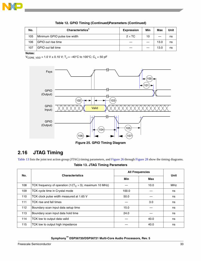
Figure 25. GPIO Timing Diagram
2.16 JTAG TimingTable 13 lists the joint test action group (JTAG) timing parameters, and Figure 26 through Figure 28 show the timing diagrams.
105 Minimum GPIO pulse low width 2 × TC 10 — ns
106 GPIO out rise time — — 13.0 ns
107 GPIO out fall time — — 13.0 ns
Notes:VCORE_VDD = 1.0 V ± 0.10 V; TJ = –40°C to 100°C; CL = 50 pF
Table 13. JTAG Timing Parameters
No. CharacteristicsAll Frequencies
Unit Min Max
108 TCK frequency of operation (1/(TC × 3); maximum 10 MHz) — 10.0 MHz
109 TCK cycle time in Crystal mode 100.0 — ns
110 TCK clock pulse width measured at 1.65 V 50.0 — ns
111 TCK rise and fall times — 3.0 ns
112 Boundary scan input data setup time 15.0 — ns
113 Boundary scan input data hold time 24.0 — ns
114 TCK low to output data valid — 40.0 ns
115 TCK low to output high impedance — 40.0 ns
Table 12. GPIO Timing (Continued)Parameters (Continued)
No. Characteristics1 Expression Min Max Unit
100
101
102 103
104 105
106 107
Fsys
Valid
GPIO(Output)
GPIOInput)
GPIO(Output)
Symphony™ DSP56720/DSP56721 Multi-Core Audio Processors, Rev. 5
Freescale Semiconductor 33
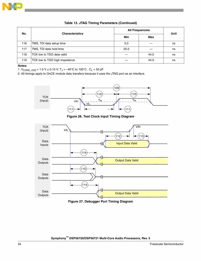
Figure 26. Test Clock Input Timing Diagram
Figure 27. Debugger Port Timing Diagram
116 TMS, TDI data setup time 5.0 — ns
117 TMS, TDI data hold time 25.0 — ns
118 TCK low to TDO data valid — 44.0 ns
119 TCK low to TDO high impedance — 44.0 ns
Notes:1. VCORE_VDD = 1.0 V ± 0.10 V; TJ = –40°C to 100°C , CL = 50 pF
2. All timings apply to OnCE module data transfers because it uses the JTAG port as an interface.
Table 13. JTAG Timing Parameters (Continued)
No. CharacteristicsAll Frequencies
Unit Min Max
109
110 110
111111
TCK(Input)
VIL
VMVIHVM
VIHVIL
113112
114
115
114
TCK(Input)
DataInputs
DataOutputs
DataOutputs
DataOutputs
Input Data Valid
Output Data Valid
Output Data Valid
Symphony™ DSP56720/DSP56721 Multi-Core Audio Processors, Rev. 5
Freescale Semiconductor34

Figure 28. Test Access Port Timing Diagram
2.17 Watchdog Timer TimingTable 14 lists the watchdog timer timing.
2.18 Host Data Interface (HDI24) TimingThe HDI24 module is only on the DSP56721 device; the DSP56720 device does not have a HDI24 module. Also, only 16 bits of the HDI24 interface are pinned out on the DSP56721 device. Table 15 lists HDI24 timing and Figure 29 through Figure 35 show the timing diagrams.
Table 14. Watchdog Timer Timing Parameters
No. Characteristics Expression Min Max Unit
120 Delay from time-out to fall of WDT, WDT_1 2 × Tc 10.0 — ns
121 Delay from timer clear to rise of WDT, WDT_1 2 × Tc 10.0 — ns
Table 15. HDI24 Timing Parameters
No. Characteristics2 Expression200 MHz
UnitMin Max
317 Read data strobe assertion width3
HACK read assertion widthTC + 9.9 14.9 — ns
318 Read data strobe deassertion width3
HACK read deassertion width— 9.9 — ns
319 Read data strobe deassertion width3 after “Last Data Register” reads4,5, or between two consecutive CVR, ICR, or ISR reads6
HACK deassertion width after “Last Data Register” reads4,5
2 × TC + 6.6 16.6 — ns
VIHVIL
116 117
118
119
118
TCK(Input)
TDITMS
(Input)
TDO(Output)
TDO(Output)
TDO(Output)
Input Data Valid
Output Data Valid
Output Data Valid
Symphony™ DSP56720/DSP56721 Multi-Core Audio Processors, Rev. 5
Freescale Semiconductor 35

320 Write data strobe assertion width7
HACK write assertion width— 13.2 — ns
321 Write data strobe deassertion width7 HACK write deassertion width • after ICR, CVR and “Last Data Register” writes4
2 × TC + 6.6 16.6 — ns
• after IVR writes, or • after TXH:TXM writes (with HBE=0), or • after TXL:TXM writes (with HBE=1)
— 16.5 — —
322 HAS assertion width — 9.9 — ns
323 HAS deassertion to data strobe assertion8 — 0.0 — ns
324 Host data input setup time before write data strobe deassertion7
Host data input setup time before HACK write deassertion— 9.9 — ns
325 Host data input hold time after write data strobe deassertion7
Host data input hold time after HACK write deassertion— 3.3 — ns
326 Read data strobe assertion to output data active from high impedance3
HACK read assertion to output data active from high impedance— 5.9 — ns
327 Read data strobe assertion to output data valid3 HACK read assertion to output data valid
— — 29.6 ns
328 Read data strobe deassertion to output data high impedance3 HACK read deassertion to output data high impedance
— — 9.9 ns
329 Output data hold time after read data strobe deassertion3 Output data hold time after HACK read deassertion
— 3.3 — ns
330 HCS assertion to read data strobe deassertion3 TC + 9.9 14.9 — ns
331 HCS assertion to write data strobe deassertion7 — 9.9 — ns
332 HCS assertion to output data valid — — 19.1 ns
333 HCS hold time after data strobe deassertion8 — 0.0 — ns
334 Address (AD7—AD0) setup time before HAS deassertion (HMUX=1) — 4.7 — ns
335 Address (AD7—AD0) hold time after HAS deassertion (HMUX=1) — 3.3 — ns
336 A10—A8 (HMUX=1), A2—A0 (HMUX=0), HR/W setup time before data strobe assertion8
• Read
— 0 — ns
• Write — 4.7 —
337 A10—A8 (HMUX=1), A2—A0 (HMUX=0), HR/W hold time after data strobe deassertion8
— 3.3 — ns
338 Delay from read data strobe deassertion to host request assertion for “Last Data Register” read3, 4, 9
TC 5.0 — ns
Table 15. HDI24 Timing Parameters (Continued)
No. Characteristics2 Expression200 MHz
UnitMin Max
Symphony™ DSP56720/DSP56721 Multi-Core Audio Processors, Rev. 5
Freescale Semiconductor36
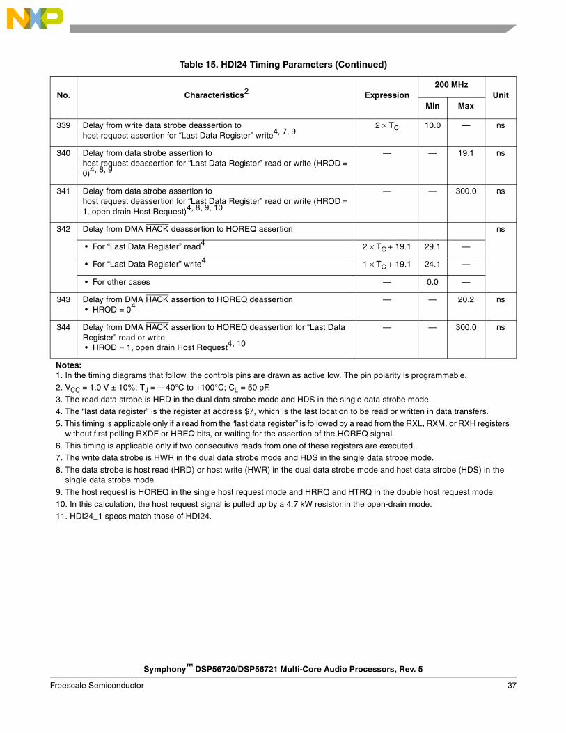
339 Delay from write data strobe deassertion to host request assertion for “Last Data Register” write4, 7, 9
2 × TC 10.0 — ns
340 Delay from data strobe assertion tohost request deassertion for “Last Data Register” read or write (HROD = 0)4, 8, 9
— — 19.1 ns
341 Delay from data strobe assertion to host request deassertion for “Last Data Register” read or write (HROD = 1, open drain Host Request)4, 8, 9, 10
— — 300.0 ns
342 Delay from DMA HACK deassertion to HOREQ assertion ns
• For “Last Data Register” read4 2 × TC + 19.1 29.1 —
• For “Last Data Register” write4 1 × TC + 19.1 24.1 —
• For other cases — 0.0 —
343 Delay from DMA HACK assertion to HOREQ deassertion • HROD = 04
— — 20.2 ns
344 Delay from DMA HACK assertion to HOREQ deassertion for “Last Data Register” read or write • HROD = 1, open drain Host Request4, 10
— — 300.0 ns
Notes:1. In the timing diagrams that follow, the controls pins are drawn as active low. The pin polarity is programmable.
2. VCC = 1.0 V ± 10%; TJ = —40°C to +100°C; CL = 50 pF.
3. The read data strobe is HRD in the dual data strobe mode and HDS in the single data strobe mode.
4. The “last data register” is the register at address $7, which is the last location to be read or written in data transfers.
5. This timing is applicable only if a read from the “last data register” is followed by a read from the RXL, RXM, or RXH registers without first polling RXDF or HREQ bits, or waiting for the assertion of the HOREQ signal.
6. This timing is applicable only if two consecutive reads from one of these registers are executed.
7. The write data strobe is HWR in the dual data strobe mode and HDS in the single data strobe mode.
8. The data strobe is host read (HRD) or host write (HWR) in the dual data strobe mode and host data strobe (HDS) in the single data strobe mode.
9. The host request is HOREQ in the single host request mode and HRRQ and HTRQ in the double host request mode.
10. In this calculation, the host request signal is pulled up by a 4.7 kW resistor in the open-drain mode.
11. HDI24_1 specs match those of HDI24.
Table 15. HDI24 Timing Parameters (Continued)
No. Characteristics2 Expression200 MHz
UnitMin Max
Symphony™ DSP56720/DSP56721 Multi-Core Audio Processors, Rev. 5
Freescale Semiconductor 37

Figure 29. HDI24 Host Interrupt Vector Register (IVR) Read Timing Diagram
Figure 30. HDI24 Read Timing Diagram, Non-Multiplexed Bus
329
317 318
328
326
327
HACK
HD23–HD0
HOREQ
327
332 319
318
317
330
329
337336
328
326
338
341
340
333
HA0–HA2
HCS
HRD, HDS
HD0–HD23
HOREQ,HRRQ,HTRQ
Symphony™ DSP56720/DSP56721 Multi-Core Audio Processors, Rev. 5
Freescale Semiconductor38
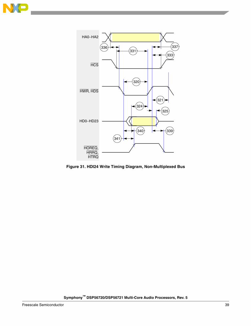
Figure 31. HDI24 Write Timing Diagram, Non-Multiplexed Bus
336331
337
321
320
324325
339340
341
333
HA0–HA2
HCS
HWR, HDS
HD0–HD23
HOREQ,HRRQ,HTRQ
Symphony™ DSP56720/DSP56721 Multi-Core Audio Processors, Rev. 5
Freescale Semiconductor 39
Figure 32. HDI24 Read Timing Diagram, Multiplexed Bus
317
318
319
328
329
327
326
335
336 337
334
341
340 338
323
322
HA8–HA10
HAS
HRD, HDS
HAD0–HAD23
HOREQ,HRRQ,HTRQ
Address Data
Symphony™ DSP56720/DSP56721 Multi-Core Audio Processors, Rev. 5
Freescale Semiconductor40

Figure 33. HDI24 Write Timing Diagram, Multiplexed Bus
Figure 34. HDI24 Host DMA Write Timing Diagram
320
321
325
324
335
341
339
336
334
340
322
323
HA8–HA10
HAS
HWR, HDS
HAD0–HAD23
HOREQ,HRRQ,HTRQ
Address Data
HOREQ(Output)
HACK(Input)
H0–H23(Input)
320 321
343342
324
344
325
TXH/M/LWrite
Data Valid
Symphony™ DSP56720/DSP56721 Multi-Core Audio Processors, Rev. 5
Freescale Semiconductor 41
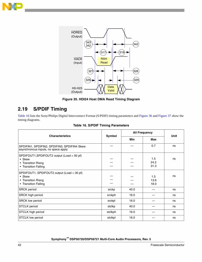
Figure 35. HDI24 Host DMA Read Timing Diagram
2.19 S/PDIF TimingTable 16 lists the Sony/Philips Digital Interconnect Format (S/PDIF) timing parameters and Figure 36 and Figure 37 show the timing diagrams.
Table 16. S/PDIF Timing Parameters
Characteristics SymbolAll Frequency
Unit Min Max
SPDIFIN1, SPDIFIN2, SPDIFIN3, SPDIFIN4 Skew: asynchronous inputs, no specs apply
— — 0.7 ns
SPDIFOUT1,SPDIFOUT2 output (Load = 50 pf) • Skew • Transition Risng • Transition Falling
———
———
1.524.231.3
ns
SPDIFOUT1, SPDIFOUT2 output (Load = 30 pf) • Skew • Transition Risng • Transition Falling
———
———
1.513.618.0
ns
SRCK period srckp 40.0 — ns
SRCK high period srckph 16.0 — ns
SRCK low period srckpl 16.0 — ns
STCLK period stclkp 40.0 — ns
STCLK high period stclkph 16.0 — ns
STCLK low period stclkpl 16.0 — ns
326
317 318
327 328
329
HOREQ(Output)
HACK(Input)
H0-H23(Output)
DataValid
RXH Read
342342343
Symphony™ DSP56720/DSP56721 Multi-Core Audio Processors, Rev. 5
Freescale Semiconductor42
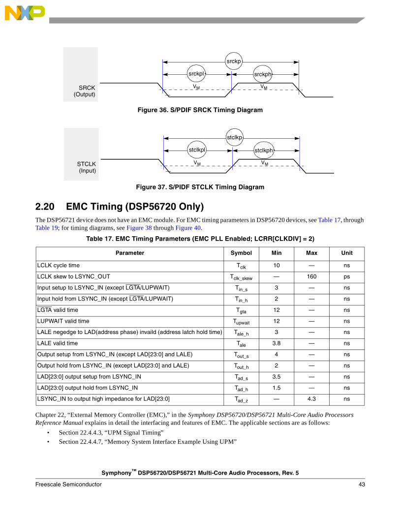
Figure 36. S/PDIF SRCK Timing Diagram
Figure 37. S/PIDF STCLK Timing Diagram
2.20 EMC Timing (DSP56720 Only)The DSP56721 device does not have an EMC module. For EMC timing parameters in DSP56720 devices, see Table 17, through Table 19; for timing diagrams, see Figure 38 through Figure 40.
Chapter 22, “External Memory Controller (EMC),” in the Symphony DSP56720/DSP56721 Multi-Core Audio Processors Reference Manual explains in detail the interfacing and features of EMC. The applicable sections are as follows:
• Section 22.4.4.3, “UPM Signal Timing”
• Section 22.4.4.7, “Memory System Interface Example Using UPM”
Table 17. EMC Timing Parameters (EMC PLL Enabled; LCRR[CLKDIV] = 2)
Parameter Symbol Min Max Unit
LCLK cycle time Tclk 10 — ns
LCLK skew to LSYNC_OUT Tclk_skew — 160 ps
Input setup to LSYNC_IN (except LGTA/LUPWAIT) Tin_s 3 — ns
Input hold from LSYNC_IN (except LGTA/LUPWAIT) Tin_h 2 — ns
LGTA valid time Tgta 12 — ns
LUPWAIT valid time Tupwait 12 — ns
LALE negedge to LAD(address phase) invaild (address latch hold time) Tale_h 3 — ns
LALE valid time Tale 3.8 — ns
Output setup from LSYNC_IN (except LAD[23:0] and LALE) Tout_s 4 — ns
Output hold from LSYNC_IN (except LAD[23:0] and LALE) Tout_h 2 — ns
LAD[23:0] output setup from LSYNC_IN Tad_s 3.5 — ns
LAD[23:0] output hold from LSYNC_IN Tad_h 1.5 — ns
LSYNC_IN to output high impedance for LAD[23:0] Tad_z — 4.3 ns
SRCK(Output)
srckp
srckphsrckpl
VMVM
STCLK(Input)
stclkp
stclkphstclkpl
VMVM
Symphony™ DSP56720/DSP56721 Multi-Core Audio Processors, Rev. 5
Freescale Semiconductor 43

Figure 38. EMC Signals (EMC PLL Enabled; LCRR[CLKDIV] = 2)
Tin_s
Tin_h
LGTA
asynchronous input
LA[2:0]/LBCTL/LCS[7:0]LOE/LWE
LCKE/LSDA10/LSDDQM
LGPL[5:0]
Output Signals
LSYNC_IN
LSYNC_OUT
LCLK
LAD[23:0] (data)
Tclk
Tclk_skew
LUPWAIT
asynchronous input
Tgta
Tupwait
Tout_s Tout_h
Tsync_in_skew
LALE
Tad_s Tad_h
LAD[23:0]
Tad_z
LSDWE/LSDRAS/LSDCAS
Tale Tale_h
Symphony™ DSP56720/DSP56721 Multi-Core Audio Processors, Rev. 5
Freescale Semiconductor44
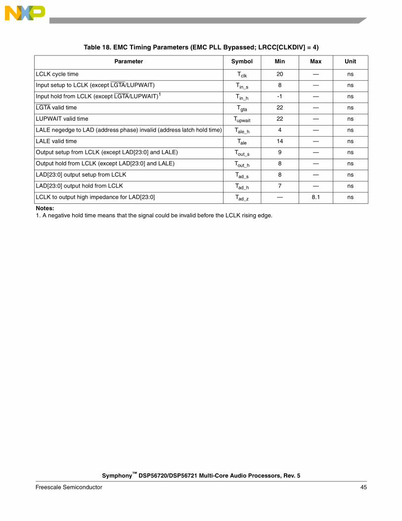
Table 18. EMC Timing Parameters (EMC PLL Bypassed; LRCC[CLKDIV] = 4)
Parameter Symbol Min Max Unit
LCLK cycle time Tclk 20 — ns
Input setup to LCLK (except LGTA/LUPWAIT) Tin_s 8 — ns
Input hold from LCLK (except LGTA/LUPWAIT)1 Tin_h -1 — ns
LGTA valid time Tgta 22 — ns
LUPWAIT valid time Tupwait 22 — ns
LALE negedge to LAD (address phase) invalid (address latch hold time) Tale_h 4 — ns
LALE valid time Tale 14 — ns
Output setup from LCLK (except LAD[23:0] and LALE) Tout_s 9 — ns
Output hold from LCLK (except LAD[23:0] and LALE) Tout_h 8 — ns
LAD[23:0] output setup from LCLK Tad_s 8 — ns
LAD[23:0] output hold from LCLK Tad_h 7 — ns
LCLK to output high impedance for LAD[23:0] Tad_z — 8.1 ns
Notes:1. A negative hold time means that the signal could be invalid before the LCLK rising edge.
Symphony™ DSP56720/DSP56721 Multi-Core Audio Processors, Rev. 5
Freescale Semiconductor 45
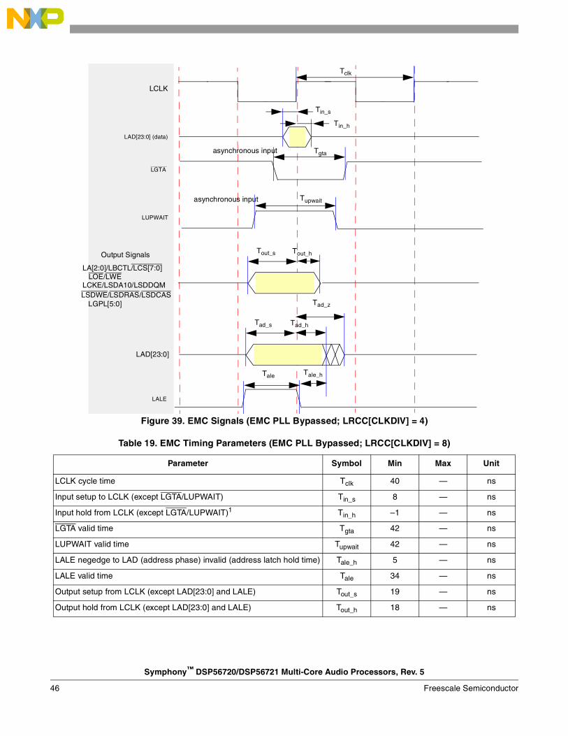
Figure 39. EMC Signals (EMC PLL Bypassed; LRCC[CLKDIV] = 4)
Table 19. EMC Timing Parameters (EMC PLL Bypassed; LRCC[CLKDIV] = 8)
Parameter Symbol Min Max Unit
LCLK cycle time Tclk 40 — ns
Input setup to LCLK (except LGTA/LUPWAIT) Tin_s 8 — ns
Input hold from LCLK (except LGTA/LUPWAIT)1 Tin_h –1 — ns
LGTA valid time Tgta 42 — ns
LUPWAIT valid time Tupwait 42 — ns
LALE negedge to LAD (address phase) invalid (address latch hold time) Tale_h 5 — ns
LALE valid time Tale 34 — ns
Output setup from LCLK (except LAD[23:0] and LALE) Tout_s 19 — ns
Output hold from LCLK (except LAD[23:0] and LALE) Tout_h 18 — ns
Tin_s
Tin_h
LGTA
asynchronous input
LA[2:0]/LBCTL/LCS[7:0]LOE/LWE
LCKE/LSDA10/LSDDQM
LGPL[5:0]
Output Signals
LCLK
LAD[23:0] (data)
Tclk
LUPWAIT
asynchronous input
Tgta
Tupwait
Tout_s Tout_h
LALE
Tad_s Tad_h
LAD[23:0]
Tad_z
LSDWE/LSDRAS/LSDCAS
Tale Tale_h
Symphony™ DSP56720/DSP56721 Multi-Core Audio Processors, Rev. 5
Freescale Semiconductor46

Figure 40. EMC Signals (EMC PLL Bypassed; LRCC[CLKDIV] = 8)
3 Functional Description and Application InformationSee the Symphony™ DSP56720/DSP56721 Multi-Core Audio Processors Reference Manual (DSP56720RM) for detailed functional and applications information.
LAD[23:0] output setup from LCLK Tad_s 12 — ns
LAD[23:0] output hold from LCLK Tad_h 17 — ns
LCLK to output high impedance for LAD[23:0] Tad_z — 17.1 ns
Notes:1. A negative hold time means that the signal could be invalid before the LCLK rising edge.
Table 19. EMC Timing Parameters (EMC PLL Bypassed; LRCC[CLKDIV] = 8) (Continued)
Parameter Symbol Min Max Unit
Tin_s
Tin_h
LGTA
asynchronous input
LA[2:0]/LBCTL/LCS[7:0]LOE/LWE
LCKE/LSDA10/LSDDQM
LGPL[5:0]
Output Signals
LCLK
LAD[23:0] (data)
Tclk
LUPWAIT
asynchronous input
Tgta
Tupwait
Tout_s Tout_h
LALE
Tad_s Tad_h
LAD[23:0]
Tad_z
LSDWE/LSDRAS/LSDCAS
Tale Tale_h
Symphony™ DSP56720/DSP56721 Multi-Core Audio Processors, Rev. 5
Freescale Semiconductor 47
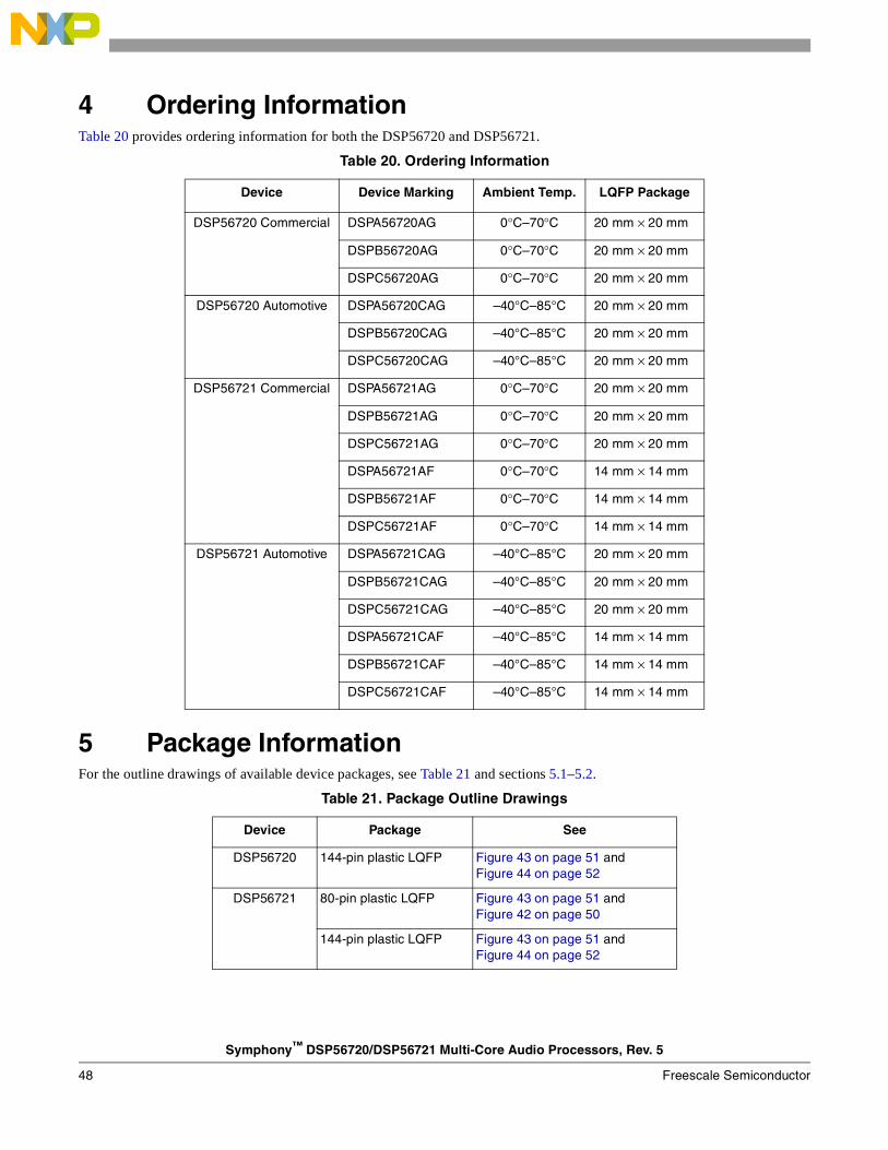
4 Ordering InformationTable 20 provides ordering information for both the DSP56720 and DSP56721.
5 Package InformationFor the outline drawings of available device packages, see Table 21 and sections 5.1–5.2.
Table 20. Ordering Information
Device Device Marking Ambient Temp. LQFP Package
DSP56720 Commercial DSPA56720AG 0°C–70°C 20 mm × 20 mm
DSPB56720AG 0°C–70°C 20 mm × 20 mm
DSPC56720AG 0°C–70°C 20 mm × 20 mm
DSP56720 Automotive DSPA56720CAG –40°C–85°C 20 mm × 20 mm
DSPB56720CAG –40°C–85°C 20 mm × 20 mm
DSPC56720CAG –40°C–85°C 20 mm × 20 mm
DSP56721 Commercial DSPA56721AG 0°C–70°C 20 mm × 20 mm
DSPB56721AG 0°C–70°C 20 mm × 20 mm
DSPC56721AG 0°C–70°C 20 mm × 20 mm
DSPA56721AF 0°C–70°C 14 mm × 14 mm
DSPB56721AF 0°C–70°C 14 mm × 14 mm
DSPC56721AF 0°C–70°C 14 mm × 14 mm
DSP56721 Automotive DSPA56721CAG –40°C–85°C 20 mm × 20 mm
DSPB56721CAG –40°C–85°C 20 mm × 20 mm
DSPC56721CAG –40°C–85°C 20 mm × 20 mm
DSPA56721CAF –40°C–85°C 14 mm × 14 mm
DSPB56721CAF –40°C–85°C 14 mm × 14 mm
DSPC56721CAF –40°C–85°C 14 mm × 14 mm
Table 21. Package Outline Drawings
Device Package See
DSP56720 144-pin plastic LQFP Figure 43 on page 51 and Figure 44 on page 52
DSP56721 80-pin plastic LQFP Figure 43 on page 51 and Figure 42 on page 50
144-pin plastic LQFP Figure 43 on page 51 and Figure 44 on page 52
Symphony™ DSP56720/DSP56721 Multi-Core Audio Processors, Rev. 5
Freescale Semiconductor48

5.1 80-Pin Package Outline DrawingFigure 41 and Figure 42 show the 80-pin package outline drawings.
Figure 41. 80-Pin Package Outline Drawing (1 of 2)
Symphony™ DSP56720/DSP56721 Multi-Core Audio Processors, Rev. 5
Freescale Semiconductor 49
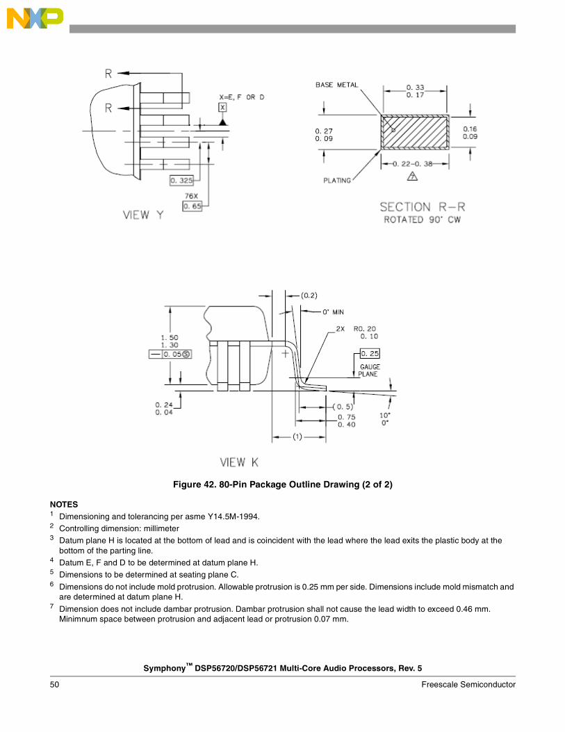
Figure 42. 80-Pin Package Outline Drawing (2 of 2)
NOTES1 Dimensioning and tolerancing per asme Y14.5M-1994.2 Controlling dimension: millimeter3 Datum plane H is located at the bottom of lead and is coincident with the lead where the lead exits the plastic body at the
bottom of the parting line.4 Datum E, F and D to be determined at datum plane H.5 Dimensions to be determined at seating plane C.6 Dimensions do not include mold protrusion. Allowable protrusion is 0.25 mm per side. Dimensions include mold mismatch and
are determined at datum plane H.7 Dimension does not include dambar protrusion. Dambar protrusion shall not cause the lead width to exceed 0.46 mm.
Minimnum space between protrusion and adjacent lead or protrusion 0.07 mm.
Symphony™ DSP56720/DSP56721 Multi-Core Audio Processors, Rev. 5
Freescale Semiconductor50
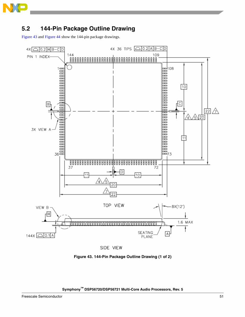
5.2 144-Pin Package Outline DrawingFigure 43 and Figure 44 show the 144-pin package drawings.
Figure 43. 144-Pin Package Outline Drawing (1 of 2)
Symphony™ DSP56720/DSP56721 Multi-Core Audio Processors, Rev. 5
Freescale Semiconductor 51

Figure 44. 144-Pin Package Outline Drawing (2 of 2)
NOTES1 All dimensinos are in millimeters2 Interpret dimensions and tolerances per ASME Y14.5M-1994.3 Datums B, C and D to be determined at datum plane H.4 The top ppackage body size may be smaller than the bottom package size by a maximum of 0.1 mm.5 These dimensions do not include mold protrusions. The maximum allowable protrusion is 0.25 mm per side. These dimensions
are maximum body size dimensions including mold mismatch.6 This dimension does not include dambar protrusion. Protrusions shall not cause the lead width to exceed 0.35 mm minimum
space between protrusion and an adjacent lead shall be 0.07 mm.
Symphony™ DSP56720/DSP56721 Multi-Core Audio Processors, Rev. 5
Freescale Semiconductor52
7 These dimensions are determined at the seating plane, datum A.
6 Product DocumentationThis Data Sheet is labeled as a particular type: Product Preview, Advance Information, or Technical Data. Definitions of these types are available at: http://www.freescale.com. Documentation is available from a local Freescale Semiconductor, Inc. distributor, semiconductor sales office, Literature Distribution Center, or through the Freescale DSP home page on the Internet (the source for the latest information).
The following documents are required for a complete description of the device and are necessary to design properly with the parts:
DSP56300 Family Manual (document number DSP56300FM). Detailed description of the 56300-family architecture and the 24-bit core processor and instruction set.
Symphony™ DSP56720/DSP56721 Multi-Core Audio Processors Reference Manual (document number DSP56720RM). Detailed description of memory, peripherals, and interfaces.
DSP56720 Product Brief (DSP56720PB). Brief description of the DSP56720 device.
DSP56721 Product Brief (DSP56721PB). Brief description of the DSP56721 device.
7 Revision HistoryTable 22 summarizes revisions to this document.
Table 22. Revision History
Revision Date Description
5 02/2009 • Updated values and added Commercial and Automotive columns in Table 4, “DC Electrical Characteristics.”
• Updated values in the following tables: Table 7, Table 9, Table 10, Table 11, Table 12, Table 13, Table 15, Table 17, Table 18, and Table 19.
• In Table 10, “Enhanced Serial Audio Interface Timing Parameters,” changed value for 87 to “13”.
• Added Section 2.4, “Power Consumption Considerations.” • In Section 2.20, “EMC Timing (DSP56720 Only),” added text regarding the EMC chapter
and applicable sections. • Added automotive information to Table 20, “Ordering Information.”
4 04/2008 • Added formula for thermal characteristics on page 10. • Added values for pull-up and pull-down resistors on page 12.
3 03/2008 • Updated order information on page 1 to include additional parts with temperature specification.
2 02/2008 • Timing updates.
1 12/2007 • Initial release
Symphony™ DSP56720/DSP56721 Multi-Core Audio Processors, Rev. 5
Freescale Semiconductor 53

How to Reach Us:
Document Number: DSP56720ECRev. 502/2009
Home Page:www.freescale.com
Web Support:http://www.freescale.com/support
USA/Europe or Locations Not Listed:Freescale Semiconductor, Inc.Technical Information Center, EL5162100 East Elliot RoadTempe, Arizona 852841-800-521-6274 or +1-480-768-2130www.freescale.com/support
Europe, Middle East, and Africa:Freescale Halbleiter Deutschland GmbHTechnical Information CenterSchatzbogen 781829 Muenchen, Germany+44 1296 380 456 (English)+46 8 52200080 (English)+49 89 92103 559 (German)+33 1 69 35 48 48 (French)www.freescale.com/support
Japan:Freescale Semiconductor Japan Ltd.HeadquartersARCO Tower 15F1-8-1, Shimo-Meguro, Meguro-ku,Tokyo 153-0064Japan0120 191014 or +81 3 5437 [email protected]
Asia/Pacific:Freescale Semiconductor China Ltd. Exchange Building 23FNo. 118 Jianguo RoadChaoyang DistrictBeijing 100022China+86 10 5879 [email protected]
For Literature Requests Only:Freescale Semiconductor Literature Distribution CenterP.O. Box 5405Denver, Colorado 802171-800-441-2447 or 303-675-2140Fax: [email protected]
Information in this document is provided solely to enable system and software implementers to use Freescale Semiconductor products. There are no express or implied copyright licenses granted hereunder to design or fabricate any integrated circuits or integrated circuits based on the information in this document.
Freescale Semiconductor reserves the right to make changes without further notice to any products herein. Freescale Semiconductor makes no warranty, representation or guarantee regarding the suitability of its products for any particular purpose, nor does Freescale Semiconductor assume any liability arising out of the application or use of any product or circuit, and specifically disclaims any and all liability, including without limitation consequential or incidental damages. “Typical” parameters that may be provided in Freescale Semiconductor data sheets and/or specifications can and do vary in different applications and actual performance may vary over time. All operating parameters, including “Typicals”, must be validated for each customer application by customer’s technical experts. Freescale Semiconductor does not convey any license under its patent rights nor the rights of others. Freescale Semiconductor products are not designed, intended, or authorized for use as components in systems intended for surgical implant into the body, or other applications intended to support or sustain life, or for any other application in which the failure of the Freescale Semiconductor product could create a situation where personal injury or death may occur. Should Buyer purchase or use Freescale Semiconductor products for any such unintended or unauthorized application, Buyer shall indemnify and hold Freescale Semiconductor and its officers, employees, subsidiaries, affiliates, and distributors harmless against all claims, costs, damages, and expenses, and reasonable attorney fees arising out of, directly or indirectly, any claim of personal injury or death associated with such unintended or unauthorized use, even if such claim alleges that Freescale Semiconductor was negligent regarding the design or manufacture of the part.
RoHS-compliant and/or Pb-free versions of Freescale products have the functionality and electrical characteristics as their non-RoHS-compliant and/or non-Pb-free counterparts. For further information, see http://www.freescale.com or contact your Freescale sales representative.
For information on Freescale’s Environmental Products program, go to http://www.freescale.com/epp.
Freescale™ and the Freescale logo are trademarks of Freescale Semiconductor, Inc. All other product or service names are the property of their respective owners.
© Freescale Semiconductor, Inc., 2009. All rights reserved.