switching theory and logic design unit-i number … notes...switching theory and logic design unit-i...
TRANSCRIPT
Switching Theory And Logic Design
UNIT-I
Number System and Boolean Algebra and Switching functions
The Decimal Number system:
The Decimal number system contains ten unique symbols. 0,1,2,3,4,5,6,7,8,9. Since
Counting in decimal involves ten symbols its base or radix is ten. There is no symbol for its
base.i.e, for ten .It is a positional weighted system i.e,the value attached to a symbol depends on
its location w.r.t. the decimalpoint.In this system, any no.(integer, fraction or mixed) of any
magnitude can be rep. by the use of these ten symbols only.Each symbol in the no. is called a
Digit. The leftmost digit in any no.rep ,which has the greatest positional weight out of all the
digits present in that no.is called the MSD (Most Significant Digit) and the right most digit
which has the least positional weight out of all the digits present in that no. is called the
LSD(Least Significant Digit).The digits on the left side of the decimal pt. form the integer part of
a decimal no. & those on the right side form the fractional part.The digits to the right of the
decimal pt have weights which are negative powers of 10 and the digits to the left of the decimal
pt have weights are positive powers of 10. The value of a decimal no.is the sum of the products
of the digit of that no. with their respective column weights. The weights of each column is 10
times greater than the weight of unity or 1010
.The first digit to the right of the decimal pt. has a
weight of 1/10 or 10-1
.for the second 1/100 & for third 1/1000.In general the value of any mixed
decimal no. is
dn dn-1 dn-2 ………d1 d0.d-1 d-2 d-3 …….d-k is given by
(dn x10n)+(dn-1 x10 n-1)+ ………(d1 x101)+(d0 x101)+(d-1 x10
2)(d-2 x10
3) …….
9’s & 10’s Complements:
It is the Subtraction of decimal no.s can be accomplished by the 9‘s & 10‘s compliment
methods similar to the 1‘s & 2‘s compliment methods of binary . the 9‘s compliment of a
decimal no. is obtained by subtracting each digit of that decimal no. from 9. The 10‘s
compliment of a decimal no is obtained by adding a 1 to its 9‘s compliment.
Example: 9‘s compliment of 3465 and 782.54 is
9999 999.99
-3465 -782.54
---------- -----------
6534 217.45 ------------------ --------------------
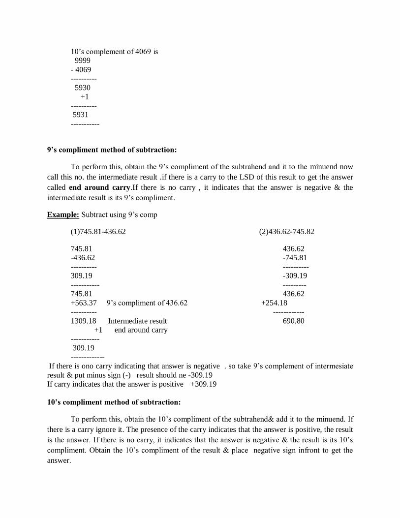
10‘s complement of 4069 is
9999
- 4069
----------
5930
+1
----------
5931
-----------
9’s compliment method of subtraction:
To perform this, obtain the 9‘s compliment of the subtrahend and it to the minuend now
call this no. the intermediate result .if there is a carry to the LSD of this result to get the answer
called end around carry.If there is no carry , it indicates that the answer is negative & the
intermediate result is its 9‘s compliment.
Example: Subtract using 9‘s comp
(1)745.81-436.62 (2)436.62-745.82
745.81 436.62
-436.62 -745.81
---------- ----------
309.19 -309.19
----------- ---------
745.81 436.62
+563.37 9‘s compliment of 436.62 +254.18
---------- ------------
1309.18 Intermediate result 690.80
+1 end around carry
-----------
309.19
-------------
If there is ono carry indicating that answer is negative . so take 9‘s complement of intermesiate
result & put minus sign (-) result should ne -309.19
If carry indicates that the answer is positive +309.19
10’s compliment method of subtraction:
To perform this, obtain the 10‘s compliment of the subtrahend& add it to the minuend. If
there is a carry ignore it. The presence of the carry indicates that the answer is positive, the result
is the answer. If there is no carry, it indicates that the answer is negative & the result is its 10‘s
compliment. Obtain the 10‘s compliment of the result & place negative sign infront to get the
answer.
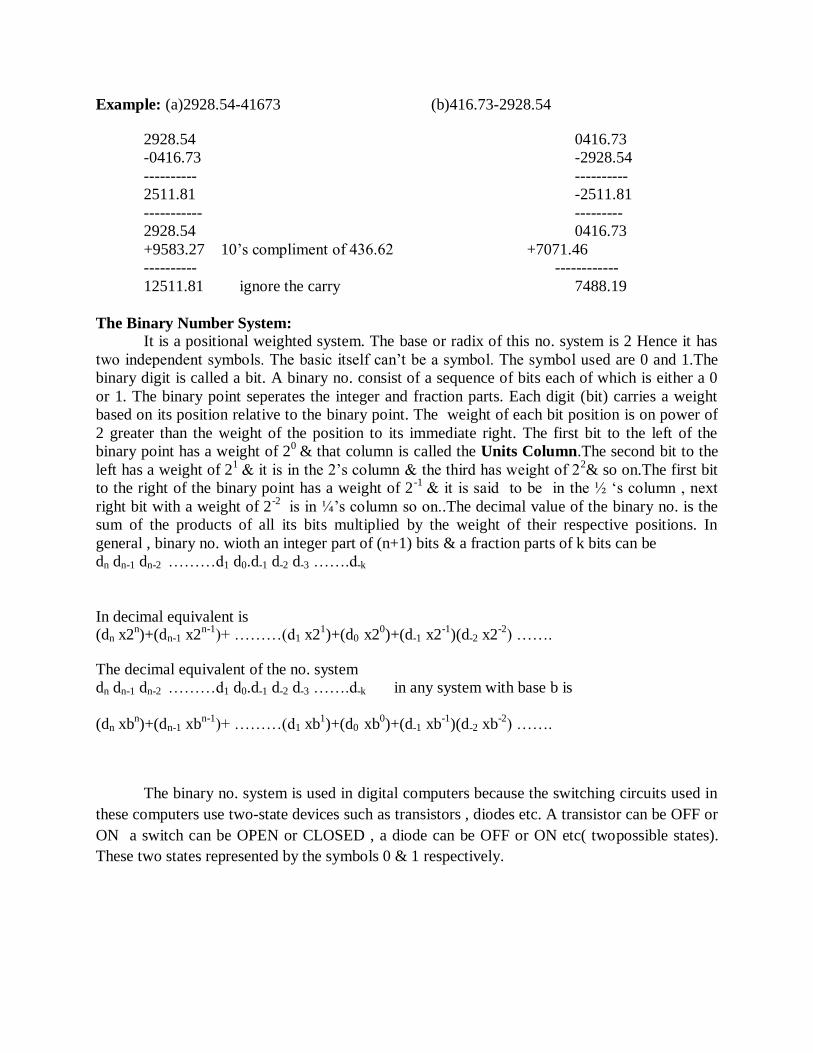
Example: (a)2928.54-41673 (b)416.73-2928.54
2928.54 0416.73
-0416.73 -2928.54
---------- ----------
2511.81 -2511.81
----------- ---------
2928.54 0416.73
+9583.27 10‘s compliment of 436.62 +7071.46
---------- ------------
12511.81 ignore the carry 7488.19
The Binary Number System:
It is a positional weighted system. The base or radix of this no. system is 2 Hence it has
two independent symbols. The basic itself can‘t be a symbol. The symbol used are 0 and 1.The
binary digit is called a bit. A binary no. consist of a sequence of bits each of which is either a 0
or 1. The binary point seperates the integer and fraction parts. Each digit (bit) carries a weight
based on its position relative to the binary point. The weight of each bit position is on power of
2 greater than the weight of the position to its immediate right. The first bit to the left of the
binary point has a weight of 20
& that column is called the Units Column.The second bit to the
left has a weight of 21
& it is in the 2‘s column & the third has weight of 22& so on.The first bit
to the right of the binary point has a weight of 2-1
& it is said to be in the ½ ‗s column , next
right bit with a weight of 2-2
is in ¼‘s column so on..The decimal value of the binary no. is the
sum of the products of all its bits multiplied by the weight of their respective positions. In
general , binary no. wioth an integer part of (n+1) bits & a fraction parts of k bits can be
dn dn-1 dn-2 ………d1 d0.d-1 d-2 d-3 …….d-k
In decimal equivalent is (dn x2
n)+(dn-1 x2
n-1)+ ………(d1 x2
1)+(d0 x2
0)+(d-1 x2
-1)(d-2 x2
-2) …….
The decimal equivalent of the no. system
dn dn-1 dn-2 ………d1 d0.d-1 d-2 d-3 …….d-k in any system with base b is
(dn xb
n)+(dn-1 xb
n-1)+ ………(d1 xb
1)+(d0 xb
0)+(d-1 xb
-1)(d-2 xb
-2) …….
The binary no. system is used in digital computers because the switching circuits used in
these computers use two-state devices such as transistors , diodes etc. A transistor can be OFF or
ON a switch can be OPEN or CLOSED , a diode can be OFF or ON etc( twopossible states).
These two states represented by the symbols 0 & 1 respectively.
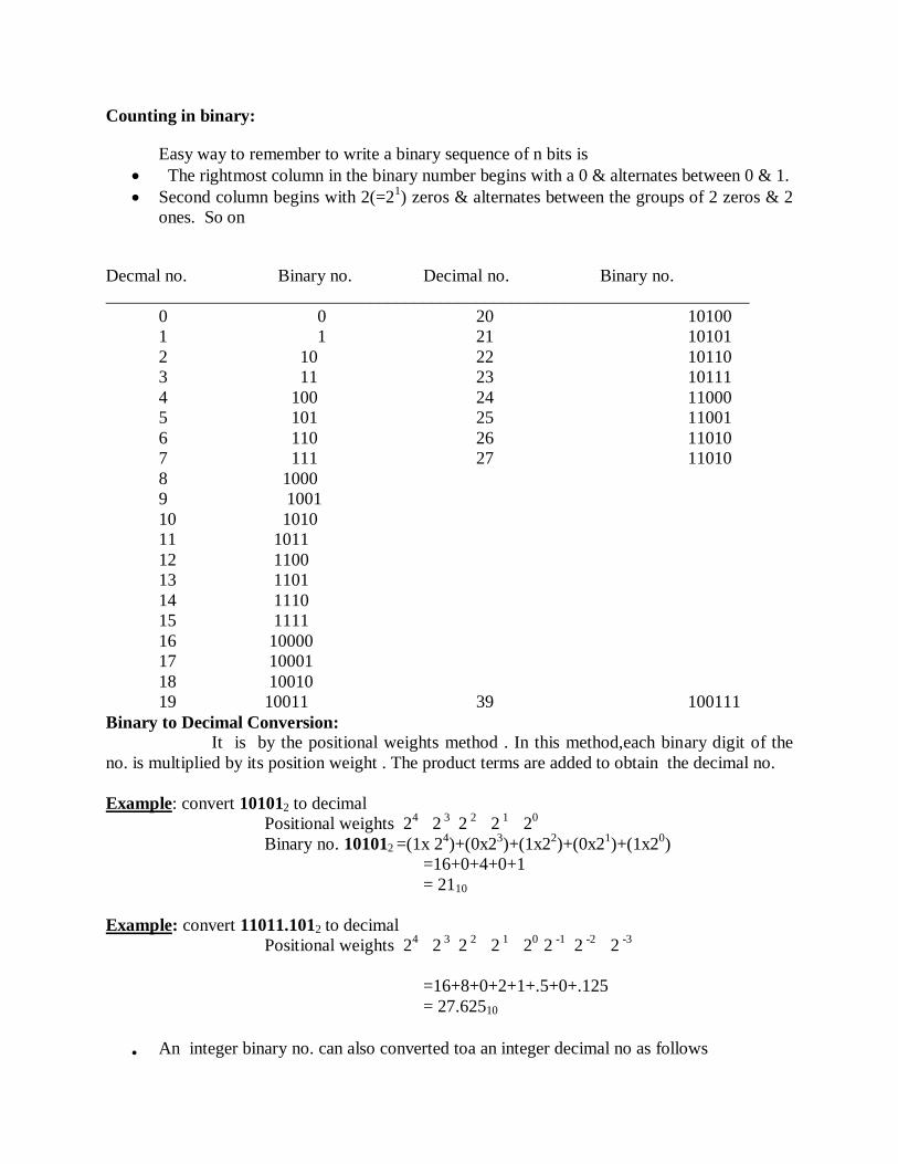
Counting in binary:
Easy way to remember to write a binary sequence of n bits is
The rightmost column in the binary number begins with a 0 & alternates between 0 & 1.
Second column begins with 2(=21) zeros & alternates between the groups of 2 zeros & 2
ones. So on
Decmal no. Binary no. Decimal no. Binary no.
_________________________________________________________________________
0 0 20 10100
1 1 21 10101
2 10 22 10110
3 11 23 10111
4 100 24 11000
5 101 25 11001
6 110 26 11010
7 111 27 11010
8 1000
9 1001
10 1010
11 1011
12 1100
13 1101
14 1110
15 1111
16 10000
17 10001
18 10010
19 10011 39 100111
Binary to Decimal Conversion:
It is by the positional weights method . In this method,each binary digit of the
no. is multiplied by its position weight . The product terms are added to obtain the decimal no.
Example: convert 101012 to decimal
Positional weights 24
2 3
2 2
2 1
20
Binary no. 101012 =(1x 2
4)+(0x2
3)+(1x2
2)+(0x2
1)+(1x2
0)
=16+0+4+0+1
= 2110
Example: convert 11011.1012 to decimal
Positional weights 24
2 3
2 2
2 1
20
2 -1
2 -2
2 -3
=16+8+0+2+1+.5+0+.125
= 27.62510
An integer binary no. can also converted toa an integer decimal no as follows
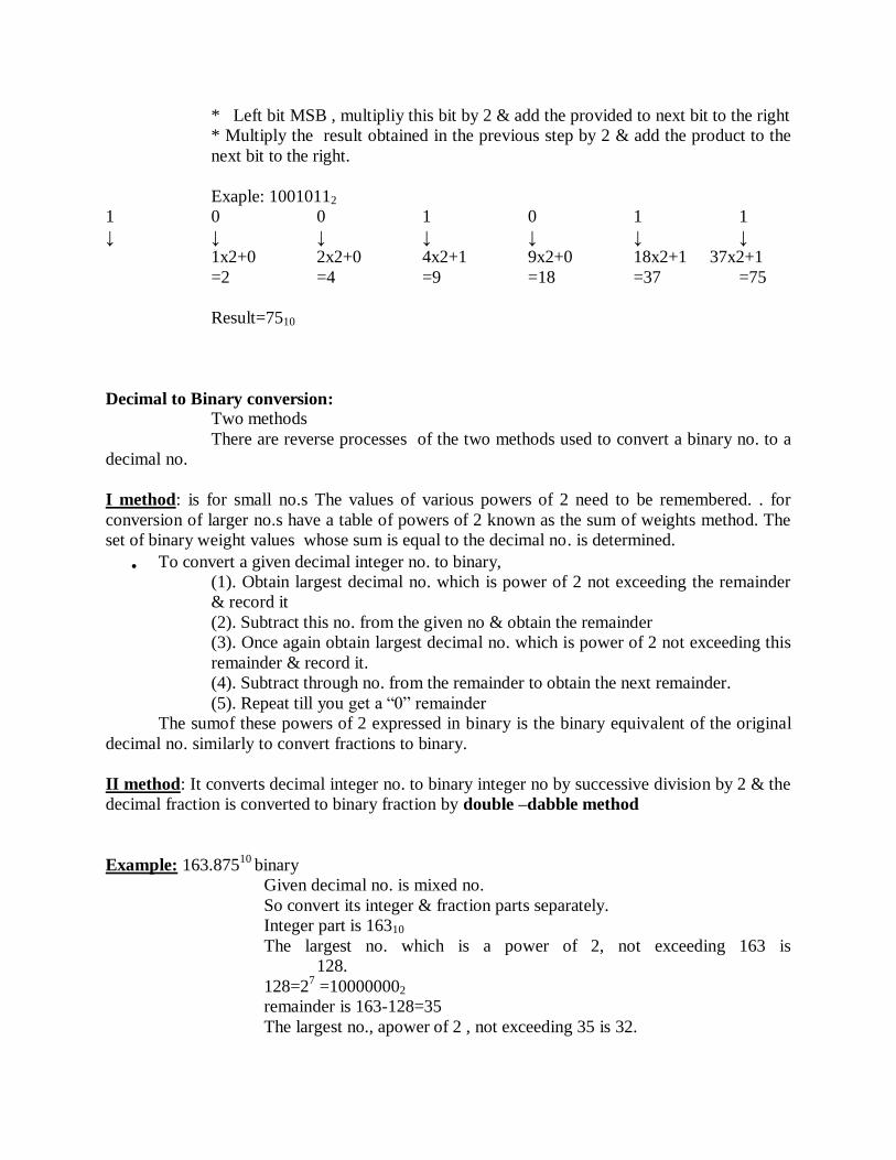
* Left bit MSB , multipliy this bit by 2 & add the provided to next bit to the right
* Multiply the result obtained in the previous step by 2 & add the product to the
next bit to the right.
Exaple: 10010112
1 0 0 1 0 1 1
↓ ↓ ↓ ↓ ↓ ↓ ↓
1x2+0 2x2+0 4x2+1 9x2+0 18x2+1 37x2+1
=2 =4 =9 =18 =37 =75
Result=7510
Decimal to Binary conversion:
Two methods
There are reverse processes of the two methods used to convert a binary no. to a
decimal no.
I method: is for small no.s The values of various powers of 2 need to be remembered. . for
conversion of larger no.s have a table of powers of 2 known as the sum of weights method. The
set of binary weight values whose sum is equal to the decimal no. is determined.
To convert a given decimal integer no. to binary,
(1). Obtain largest decimal no. which is power of 2 not exceeding the remainder
& record it
(2). Subtract this no. from the given no & obtain the remainder
(3). Once again obtain largest decimal no. which is power of 2 not exceeding this
remainder & record it.
(4). Subtract through no. from the remainder to obtain the next remainder.
(5). Repeat till you get a ―0‖ remainder
The sumof these powers of 2 expressed in binary is the binary equivalent of the original
decimal no. similarly to convert fractions to binary.
II method: It converts decimal integer no. to binary integer no by successive division by 2 & the
decimal fraction is converted to binary fraction by double –dabble method
Example: 163.87510
binary
Given decimal no. is mixed no.
So convert its integer & fraction parts separately.
Integer part is 16310
The largest no. which is a power of 2, not exceeding 163 is
128.
128=27 =100000002
remainder is 163-128=35
The largest no., apower of 2 , not exceeding 35 is 32.
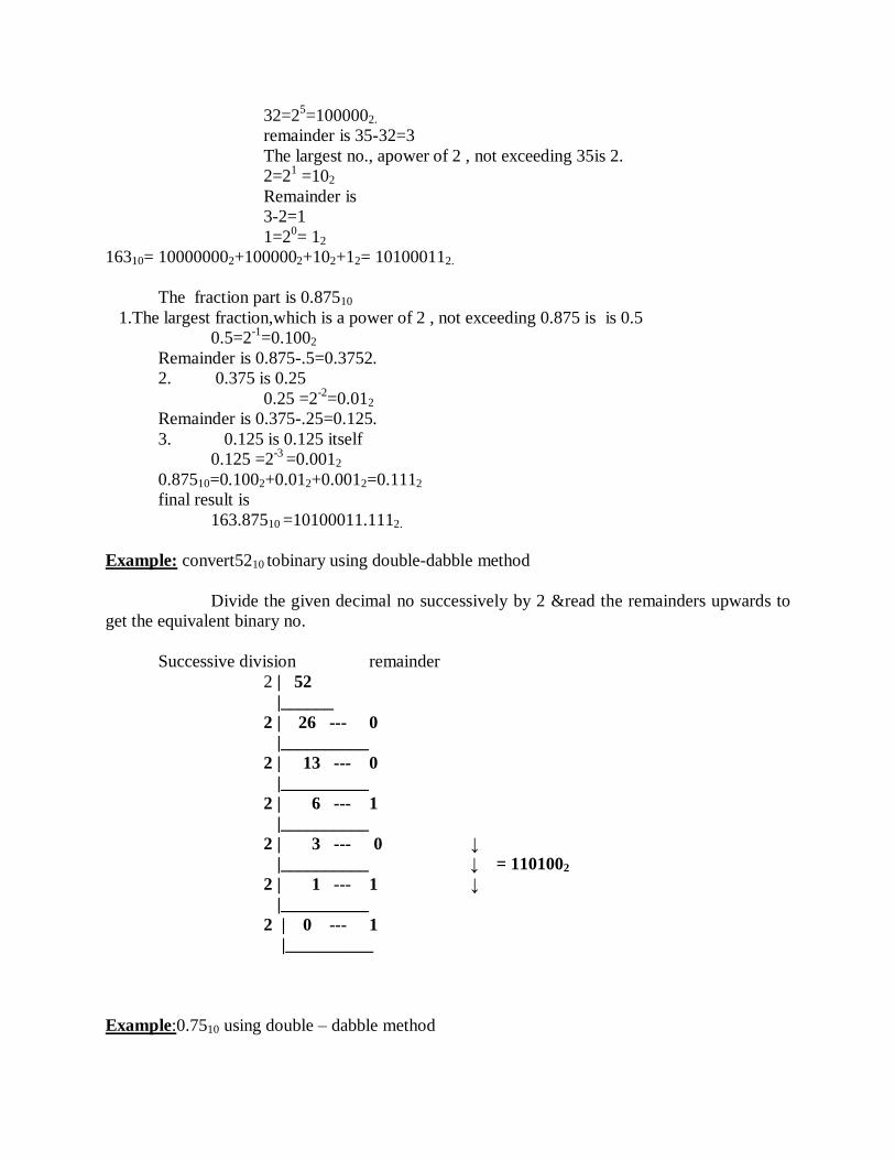
32=25=1000002.
remainder is 35-32=3
The largest no., apower of 2 , not exceeding 35is 2.
2=21 =102
Remainder is
3-2=1
1=20= 12
16310= 100000002+1000002+102+12= 101000112.
The fraction part is 0.87510
1.The largest fraction,which is a power of 2 , not exceeding 0.875 is is 0.5
0.5=2-1
=0.1002
Remainder is 0.875-.5=0.3752.
2. 0.375 is 0.25
0.25 =2-2
=0.012
Remainder is 0.375-.25=0.125.
3. 0.125 is 0.125 itself
0.125 =2-3
=0.0012
0.87510=0.1002+0.012+0.0012=0.1112
final result is
163.87510 =10100011.1112.
Example: convert5210 tobinary using double-dabble method
Divide the given decimal no successively by 2 &read the remainders upwards to
get the equivalent binary no.
Successive division remainder
2 | 52
|______
2 | 26 --- 0
|__________
2 | 13 --- 0
|__________
2 | 6 --- 1
|__________
2 | 3 --- 0 ↓
|__________ ↓ = 1101002
2 | 1 --- 1 ↓
|__________
2 | 0 --- 1
|__________
Example:0.7510 using double – dabble method
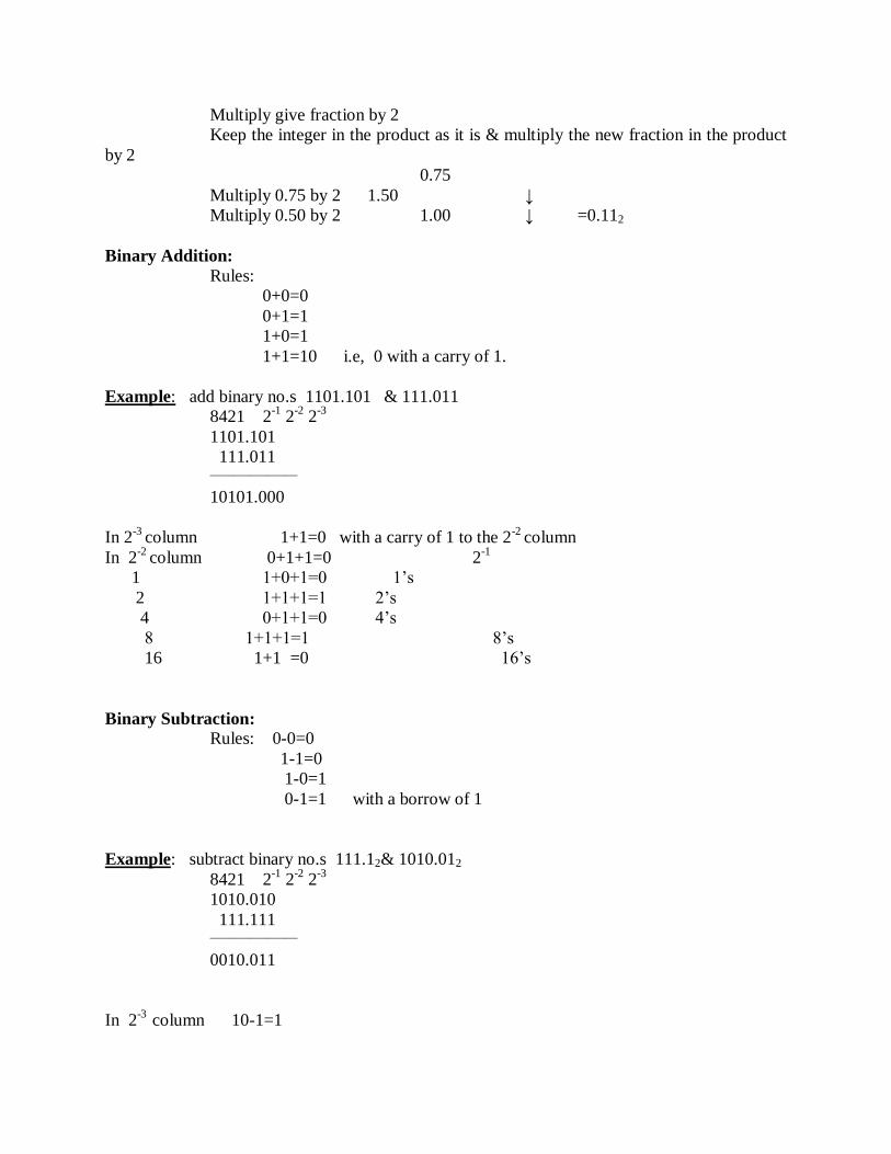
Multiply give fraction by 2
Keep the integer in the product as it is & multiply the new fraction in the product
by 2
0.75
Multiply 0.75 by 2 1.50 ↓
Multiply 0.50 by 2 1.00 ↓ =0.112
Binary Addition:
Rules:
0+0=0
0+1=1
1+0=1
1+1=10 i.e, 0 with a carry of 1.
Example: add binary no.s 1101.101 & 111.011
8421 2-1
2-2
2-3
1101.101
111.011
_______________
10101.000
In 2-3
column 1+1=0 with a carry of 1 to the 2-2
column
In 2-2
column 0+1+1=0 2-1
1 1+0+1=0 1‘s
2 1+1+1=1 2‘s
4 0+1+1=0 4‘s
8 1+1+1=1 8‘s
16 1+1 =0 16‘s
Binary Subtraction:
Rules: 0-0=0
1-1=0
1-0=1
0-1=1 with a borrow of 1
Example: subtract binary no.s 111.12& 1010.012
8421 2-1
2-2
2-3
1010.010
111.111
_______________
0010.011
In 2-3
column 10-1=1
2-2
10-1=1
2-1
1-1=0
1‘s 1-1=0
2‘s 10-1=1
4‘s 1-1=0
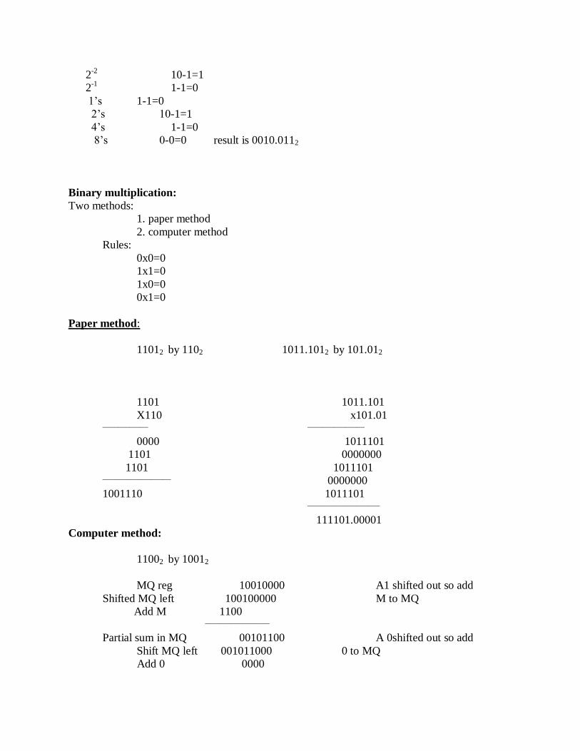
8‘s 0-0=0 result is 0010.0112
Binary multiplication:
Two methods:
1. paper method
2. computer method
Rules:
0x0=0
1x1=0
1x0=0
0x1=0
Paper method:
11012 by 1102 1011.1012 by 101.012
1101 1011.101
X110 x101.01
____________ _______________
0000 1011101
1101 0000000
1101 1011101
__________________
0000000
1001110 1011101
___________________
111101.00001
Computer method:
11002 by 10012
MQ reg 10010000 A1 shifted out so add
Shifted MQ left 100100000 M to MQ
Add M 1100
_________________
Partial sum in MQ 00101100 A 0shifted out so add
Shift MQ left 001011000 0 to MQ
Add 0 0000
__________________
Partial sum in MQ 01011000 A 0shifted out so add
Shift MQ left 010110000 0 to MQ
Add 0 0000
___________________
Partial sum in MQ
101100000 A1 shifted out so add
Shift MQ left 101100000 M to MQ
Add M 1100
_______________________
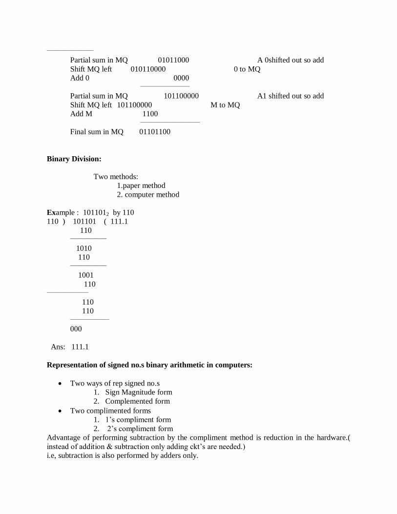
Final sum in MQ 01101100
Binary Division:
Two methods:
1.paper method
2. computer method
Example : 1011012 by 110
110 ) 101101 ( 111.1
110
______________
1010
110
______________
1001
110 ________________
110
110
_______________
000
Ans: 111.1
Representation of signed no.s binary arithmetic in computers:
Two ways of rep signed no.s
1. Sign Magnitude form
2. Complemented form
Two complimented forms
1. 1‘s compliment form
2. 2‘s compliment form
Advantage of performing subtraction by the compliment method is reduction in the hardware.(
instead of addition & subtraction only adding ckt‘s are needed.)
i.e, subtraction is also performed by adders only.
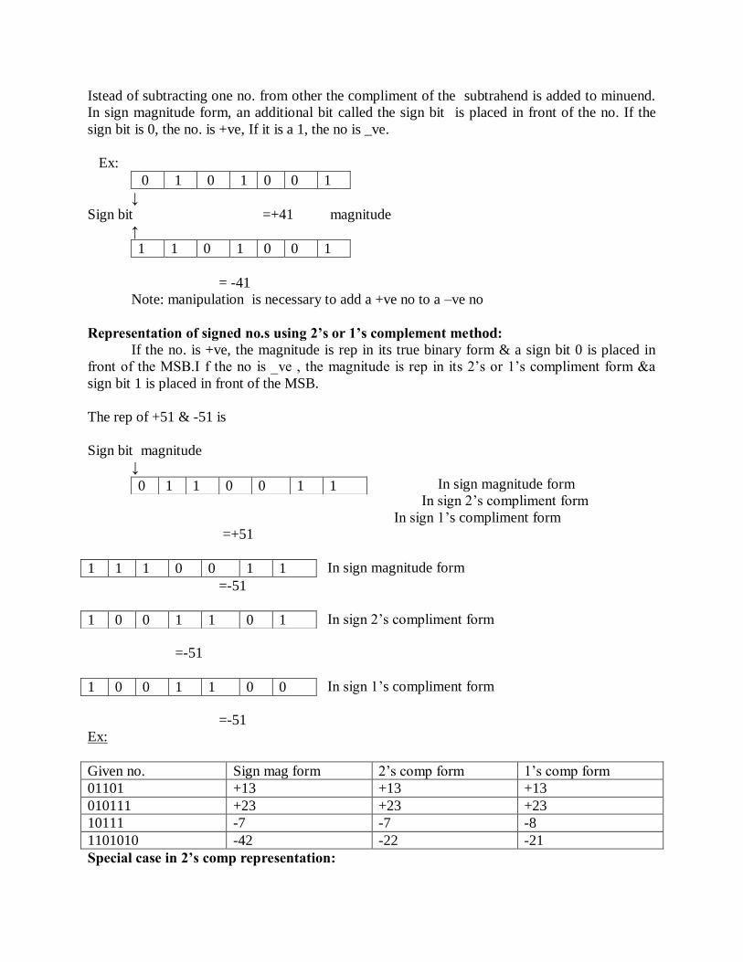
Istead of subtracting one no. from other the compliment of the subtrahend is added to minuend.
In sign magnitude form, an additional bit called the sign bit is placed in front of the no. If the
sign bit is 0, the no. is +ve, If it is a 1, the no is _ve.
Ex:
0 1 0 1 0 0 1
↓
Sign bit =+41 magnitude
↑
1 1 0 1 0 0 1
= -41
Note: manipulation is necessary to add a +ve no to a –ve no
Representation of signed no.s using 2’s or 1’s complement method:
If the no. is +ve, the magnitude is rep in its true binary form & a sign bit 0 is placed in
front of the MSB.I f the no is _ve , the magnitude is rep in its 2‘s or 1‘s compliment form &a
sign bit 1 is placed in front of the MSB.
The rep of +51 & -51 is
Sign bit magnitude
↓
In sign magnitude form
In sign 2‘s compliment form
In sign 1‘s compliment form
=+51
In sign magnitude form
=-51
In sign 2‘s compliment form
=-51
In sign 1‘s compliment form
=-51
Ex:
Given no. Sign mag form 2‘s comp form 1‘s comp form
01101 +13 +13 +13
010111 +23 +23 +23
10111 -7 -7 -8
1101010 -42 -22 -21
Special case in 2’s comp representation:
0 1 1 0 0 1 1
1 1 1 0 0 1 1
1 0 0 1 1 0 1
1 0 0 1 1 0 0
Whenever a signed no. has a 1 in the sign bit & all 0‘s for the magnitude bits, the decimal
equivalent is -2n , where n is the no of bits in the magnitude .
Ex: 1000= -8 & 10000=-16
Characteristics of 2’s compliment no.s:
Properties:
1. There is one unique zero
2. 2‘s comp of 0 is 0
3. The leftmost bit can‘t be used to express a quantity . it is a 0 no. is +ve.
4. For an n-bit word which includes the sign bit there are (2n-1
-1) +ve integers,
2n-1
–ve integers & one 0 , for a total of 2n unique states.
5. Significant information is containd in the 1‘s of the +ve no.s & 0‘s of the _ve
no.s
6. A _ve no. may be converted into a +ve no. by finding its 2‘s comp.
Signed binary numbers:
Decimal Sign 2‘s comp form Sign 1‘s comp form Sign mag form
+7 0111 0111 0111
+6 0110 0110 0110
+5 0101 0101 0101
+4 0100 0100 0100
+3 0011 0011 0011
+2 0010 0010 0010
+1 0011 0011 0011
+0 0000 0000 0000
-0 -- 1111 1000
-1 1111 1110 1001
-2 1110 1101 1010
-3 1101 1100 1011
-4 1100 1011 1100
-5 1011 1010 1101
-6 1010 1001 1110
-7 1001 1000 1111
8 1000 -- --
Methods of obtaining 2’s comp of a no:
In 3 ways
1. By obtaining the 1‘s comp of the given no. (by changing all 0‘s to 1‘s & 1‘s to 0‘s) &
then adding 1.
2. By subtracting the given n bit no N from 2n
3. Starting at the LSB , copying down each bit upto & including the first 1 bit
encountered , and complimenting the remaining bits.
Ex: Express -45 in 8 bit 2‘s comp form
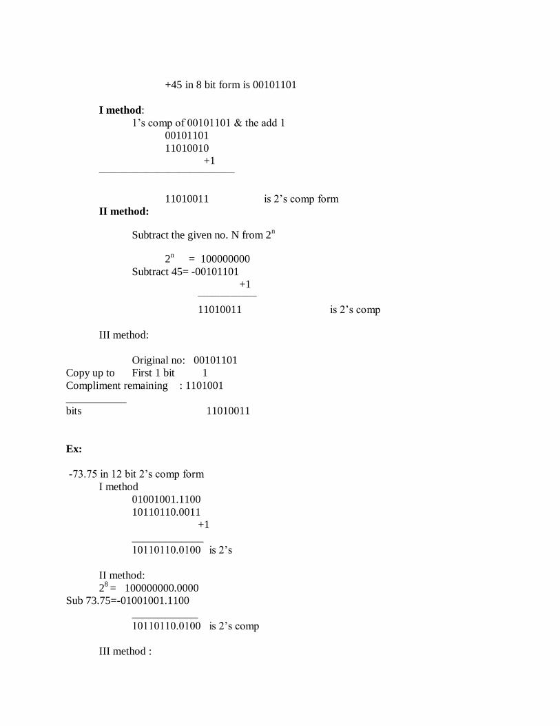
+45 in 8 bit form is 00101101
I method:
1‘s comp of 00101101 & the add 1
00101101
11010010
+1 _____________________________________
11010011 is 2‘s comp form
II method:
Subtract the given no. N from 2n
2n
= 100000000
Subtract 45= -00101101
+1
________________
11010011 is 2‘s comp
III method:
Original no: 00101101
Copy up to First 1 bit 1
Compliment remaining : 1101001
___________
bits 11010011
Ex:
-73.75 in 12 bit 2‘s comp form
I method
01001001.1100
10110110.0011
+1
_____________
10110110.0100 is 2‘s
II method:
28 = 100000000.0000
Sub 73.75=-01001001.1100
____________
10110110.0100 is 2‘s comp
III method :
Orginalno : 01001001.1100
Copy up to 1‘st bit : 100
Comp the remaining bits: 10110110.0
_____________
10110110.0100
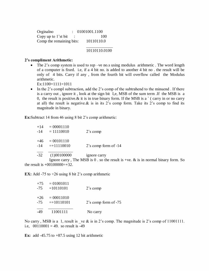
2’s compliment Arithmetic:
The 2‘s comp system is used to rep –ve no.s using modulus arithmetic . The word length
of a computer is fixed. i.e, if a 4 bit no. is added to another 4 bit no . the result will be
only of 4 bits. Carry if any , from the fourth bit will overflow called the Modulus
arithmetic.
Ex:1100+1111=1011
In the 2‘s compl subtraction, add the 2‘s comp of the subtrahend to the minuend . If there
is a carry out , ignore it , look at the sign bit I,e, MSB of the sum term .If the MSB is a
0, the result is positive.& it is in true binary form. If the MSB is a ` ( carry in or no carry
at all) the result is negative.& is in its 2‘s comp form. Take its 2‘s comp to find its
magnitude in binary.
Ex:Subtract 14 from 46 using 8 bit 2‘s comp arithmetic:
+14 = 00001110
-14 = 11110010 2‘s comp
+46 = 00101110
-14 =+11110010 2‘s comp form of -14
___ ____________
-32 (1)00100000 ignore carry
Ignore carry , The MSB is 0 . so the result is +ve. & is in normal binary form. So
the result is +00100000=+32.
EX: Add -75 to +26 using 8 bit 2‘s comp arithmetic
+75 = 01001011
-75 =10110101 2‘s comp
+26 = 00011010
-75 =+10110101 2‘s comp form of -75
___ ____________
-49 11001111 No carry
No carry , MSB is a 1, result is _ve & is in 2‘s comp. The magnitude is 2‘s comp of 11001111.
i.e, 00110001 = 49. so result is -49
Ex: add -45.75 to +87.5 using 12 bit arithmetic
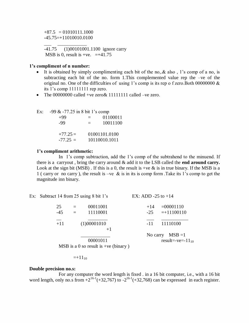
+87.5 = 01010111.1000
-45.75=+11010010.0100
___ ____________
-41.75 (1)00101001.1100 ignore carry
MSB is 0, result is +ve. =+41.75
1’s compliment of n number:
It is obtained by simply complimenting each bit of the no,.& also , 1‘s comp of a no, is
subtracting each bit of the no. form 1.This complemented value rep the –ve of the
original no. One of the difficulties of using 1‘s comp is its rep o f zero.Both 00000000 &
its 1‘s comp 11111111 rep zero.
The 00000000 called +ve zero& 11111111 called –ve zero.
Ex: -99 & -77.25 in 8 bit 1‘s comp
+99 = 01100011
-99 = 10011100
+77.25 = 01001101.0100
-77.25 = 10110010.1011
1’s compliment arithmetic:
In 1‘s comp subtraction, add the 1‘s comp of the subtrahend to the minuend. If
there is a carryout , bring the carry around & add it to the LSB called the end around carry.
Look at the sign bit (MSB) . If this is a 0, the result is +ve & is in true binary. If the MSB is a
1 ( carry or no carry ), the result is –ve & is in its is comp form .Take its 1‘s comp to get the
magnitude inn binary.
Ex: Subtract 14 from 25 using 8 bit 1‘s EX: ADD -25 to +14
25 = 00011001 +14 =00001110
-45 = 11110001 -25 =+11100110
__ ________ ___ ___________
+11 (1)00001010 -11 11110100
+1
____________ No carry MSB =1
00001011 result=-ve=-1110
MSB is a 0 so result is +ve (binary )
=+1110
Double precision no.s:
For any computer the word length is fixed . in a 16 bit computer, i.e., with a 16 bit
word length, only no.s from +216-1
(+32,767) to -216-1
(+32,768) can be expressed in each register.
If no. is greater than this, two storage locations need to be used. i.e, each such no. has to be
stored in two registers called Double Precision.
Leaving the MSB which is the sign bit, allows a 31 bit no. length with two 16 bit
registers. If still larger no.s are to be expressed, there registers are used to store each no. called
Triple Precision.
Floating Point NO.s:
In decimal system, very large & very small no.s expressed in scientific notation by
stating a no. (mantissa) & an exponent of 10.
Binary no.s can be expressed in same notation by an exponent of 2.
Mantissa Exponent
0110000000 100101
16 bit word contains two parts:10 bit mantissa , 6 bit exponent.i.e, in 2‘s comp form & in that
MSB is sign bit.
Many formats of floating pt.no.s.Someuse 2 words for mantissa, one for exponent .other use 2 &
half words for mantissa & half for exponent.
Depending on the accuracy desired. some use excess n notation for the exponent, some use 2‘s
comp notation for mantissa &some use sign magnitude for both mantissa & exponent.
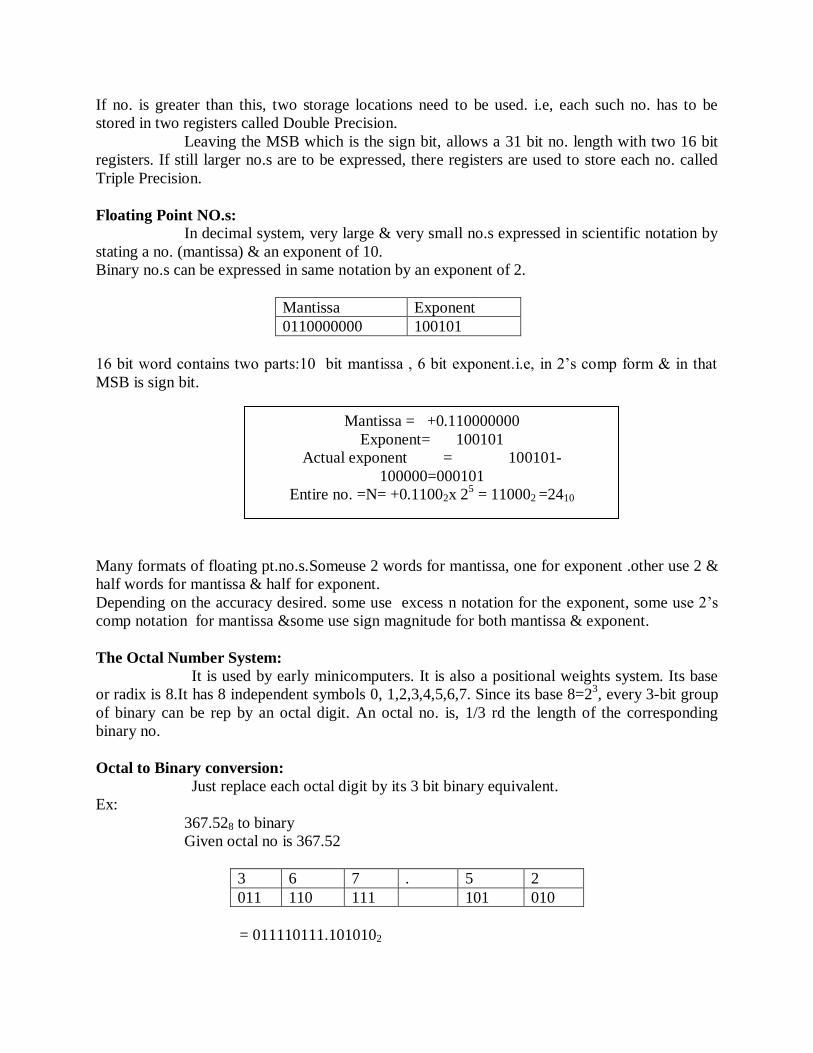
The Octal Number System:
It is used by early minicomputers. It is also a positional weights system. Its base
or radix is 8.It has 8 independent symbols 0, 1,2,3,4,5,6,7. Since its base 8=23, every 3-bit group
of binary can be rep by an octal digit. An octal no. is, 1/3 rd the length of the corresponding
binary no.
Octal to Binary conversion:
Just replace each octal digit by its 3 bit binary equivalent.
Ex:
367.528 to binary
Given octal no is 367.52
3 6 7 . 5 2
011 110 111 101 010
= 011110111.1010102
Mantissa = +0.110000000
Exponent= 100101
Actual exponent = 100101-
100000=000101
Entire no. =N= +0.11002x 25 = 110002 =2410
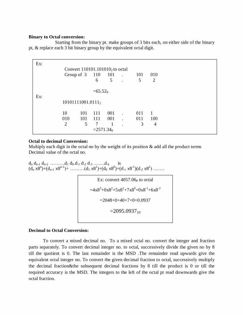
Binary to Octal conversion:
Starting from the binary pt. make groups of 3 bits each, on either side of the binary
pt, & replace each 3 bit binary group by the equivalent octal digit.
Octal to decimal Conversion:
Multiply each digit in the octal no by the weight of its position & add all the product terms
Decimal value of the octal no.
dn dn-1 dn-2 ………d1 d0.d-1 d-2 d-3 …….d-k is (dn x8
n)+(dn-1 x8
n-1)+ ………(d1 x8
1)+(d0 x8
0)+(d-1 x8
-1)(d-2 x8
2) …….
Decimal to Octal Conversion:
To convert a mixed decimal no. To a mixed octal no. convert the integer and fraction
parts separately. To convert decimal integer no. to octal, successively divide the given no by 8
till the quotient is 0. The last remainder is the MSD .The remainder read upwards give the
equivalent octal integer no. To convert the given decimal fraction to octal, successively multiply
the decimal fraction&the subsequent decimal fractions by 8 till the product is 0 or till the
required accuracy is the MSD. The integers to the left of the octal pt read downwards give the
octal fraction.
Ex: convert 4057.068 to octal
=4x83+0x8
2+5x8
1+7x8
0+0x8
-1+6x8
-2
=2048+0+40+7+0+0.0937
=2095.093710
Ex:
Convert 110101.1010102 to octal
Group of 3 110 101 . 101 010
6 5 . 5 2
=65.528
Ex:
10101111001.01112
10 101 111 001 . 011 1
010 101 111 001 . 011 100
2 5 7 1 . 3 4
=2571.348
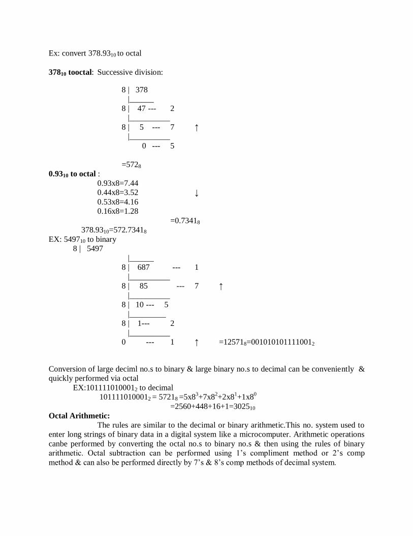
Ex: convert 378.9310 to octal
37810 tooctal: Successive division:
8 | 378
|______
8 | 47 --- 2
|__________
8 | 5 --- 7 ↑
|__________
0 --- 5
=5728
0.9310 to octal :
0.93x8=7.44
0.44x8=3.52 ↓
0.53x8=4.16
0.16x8=1.28
=0.73418
378.9310=572.73418
EX: 549710 to binary
8 | 5497
|______
8 | 687 --- 1
|__________
8 | 85 --- 7 ↑
|__________
8 | 10 --- 5
|_________
8 | 1--- 2
|__________
0 --- 1 ↑ =125718=0010101011110012
Conversion of large deciml no.s to binary & large binary no.s to decimal can be conveniently &
quickly performed via octal
EX:1011110100012 to decimal
1011110100012 = 57218 =5x83+7x8
2+2x8
1+1x8
0
=2560+448+16+1=302510
Octal Arithmetic:
The rules are similar to the decimal or binary arithmetic.This no. system used to
enter long strings of binary data in a digital system like a microcomputer. Arithmetic operations
canbe performed by converting the octal no.s to binary no.s & then using the rules of binary
arithmetic. Octal subtraction can be performed using 1‘s compliment method or 2‘s comp
method & can also be performed directly by 7‘s & 8‘s comp methods of decimal system.

Multiplication & division can slso be performed using the binary rep. of octal no.s &
then making use of multiplication & division rules of binary no.s
The Hexadecimal number system:
Binary no.s are long & fine for machines but are too lengthy to be handled by human
benigs. So rep binary no.s concisely with their objective is the hexadecimal no system( or hex) .
It is a positional weighted system.The base or radix of there is 16 i.e, it has 16 independent
symbols 0,1,2,----9,A,B,C,D,E,F. since its base is 16=24, every 4 binary digit combination can be
rep by one hexa decimal digit . so a hexadecimal no is ¼ th the length of the corresponding
binary no..A 4 bit group is nibble.
Hexadecimal counting system:
0 1 2 3 4 5 6 7 8 9 A B C D E F
10 11 12 13 14 15 16 17 18 19 1A 1B 1C 1D 1E 1F
: ;
: :
: :
F0 F1 F2------------------------------------------------------------------------FF
100 101 -----------------------------------------------------------------------10F
: :
: :
1F0 1F1------------------------------------------------------------------------1FF
Ex: Add (27.5)8 (74.4)8 Subtract 458 from 668
27.58 = 010 111 . 1012 668 =00 110 1102
+74.48 = +1111000.1002 -458 =+11 011 0112
_____ ____________ ___ ___________
124.18 1010 100. 001 (1)00 010 0012
Ignore carry ans: +ve.
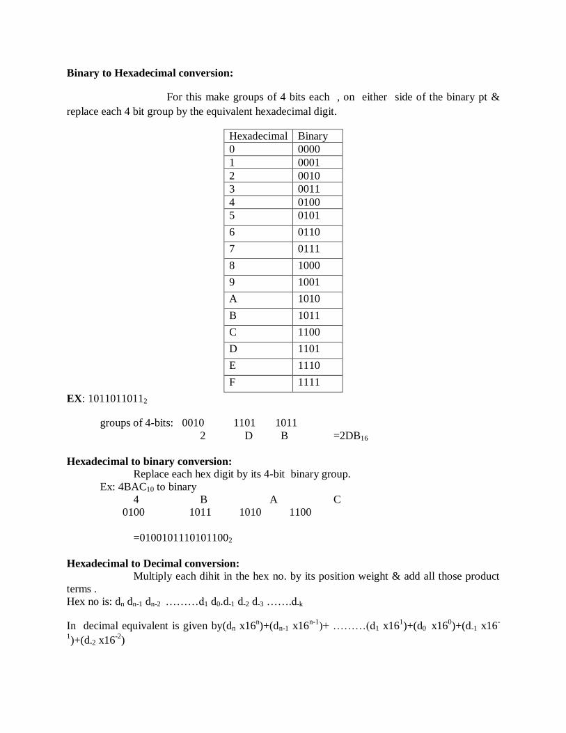
Binary to Hexadecimal conversion:
For this make groups of 4 bits each , on either side of the binary pt &
replace each 4 bit group by the equivalent hexadecimal digit.
Hexadecimal Binary
0 0000
1 0001
2 0010
3 0011
4 0100
5 0101
6 0110
7 0111
8 1000
9 1001
A 1010
B 1011
C 1100
D 1101
E 1110
F 1111
EX: 10110110112
groups of 4-bits: 0010 1101 1011
2 D B =2DB16
Hexadecimal to binary conversion:
Replace each hex digit by its 4-bit binary group.
Ex: 4BAC10 to binary
4 B A C
0100 1011 1010 1100
=01001011101011002
Hexadecimal to Decimal conversion:
Multiply each dihit in the hex no. by its position weight & add all those product
terms .
Hex no is: dn dn-1 dn-2 ………d1 d0.d-1 d-2 d-3 …….d-k
In decimal equivalent is given by(dn x16n)+(dn-1 x16
n-1)+ ………(d1 x16
1)+(d0 x16
0)+(d-1 x16
-
1)+(d-2 x16
-2)
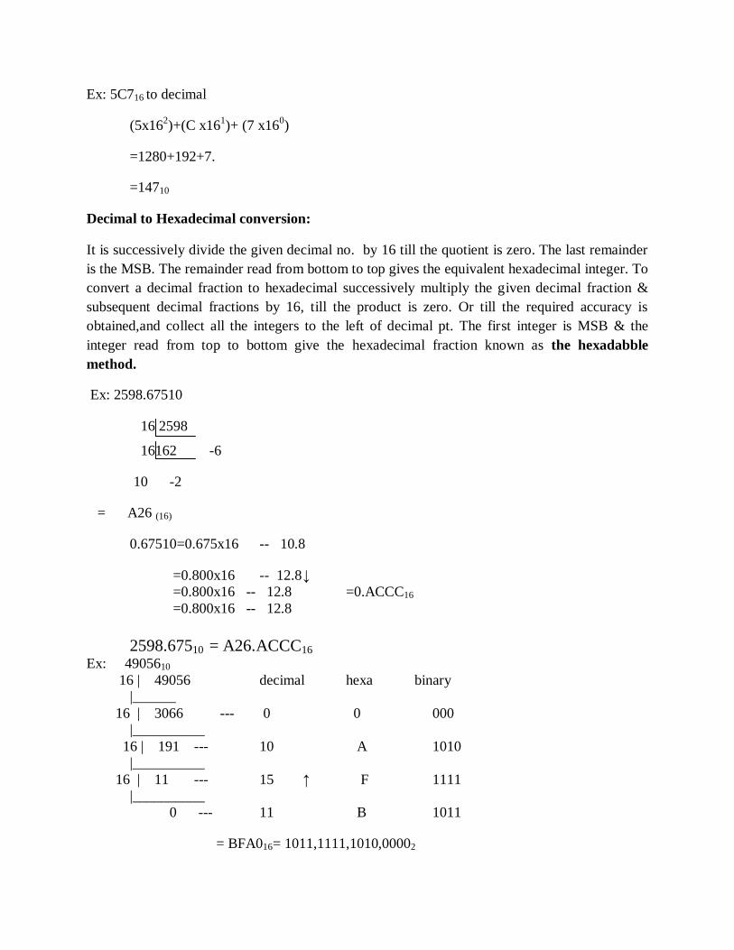
Ex: 5C716 to decimal
(5x162)+(C x16
1)+ (7 x16
0)
=1280+192+7.
=14710
Decimal to Hexadecimal conversion:
It is successively divide the given decimal no. by 16 till the quotient is zero. The last remainder
is the MSB. The remainder read from bottom to top gives the equivalent hexadecimal integer. To
convert a decimal fraction to hexadecimal successively multiply the given decimal fraction &
subsequent decimal fractions by 16, till the product is zero. Or till the required accuracy is
obtained,and collect all the integers to the left of decimal pt. The first integer is MSB & the
integer read from top to bottom give the hexadecimal fraction known as the hexadabble
method.
Ex: 2598.67510
16 2598
16162 -6
10 -2
= A26 (16)
0.67510=0.675x16 -- 10.8
=0.800x16 -- 12.8 ↓
=0.800x16 -- 12.8 =0.ACCC16
=0.800x16 -- 12.8
2598.67510 = A26.ACCC16 Ex: 4905610
16 | 49056 decimal hexa binary
|______
16 | 3066 --- 0 0 000
|__________
16 | 191 --- 10 A 1010
|__________
16 | 11 --- 15 ↑ F 1111
|__________
0 --- 11 B 1011
= BFA016= 1011,1111,1010,00002

Octal to hexadecimal conversion:
The simplest way is to first convert the given octal no. to binary & then the binary no. to
hexadecimal.
Ex: 756.6038
7 5 6 . 6 0 3
111 101 110 . 110 000 011
0001 1110 1110 . 1100 0001 1000
1 E E . C 1 8
Hexa decimal to octal conversion:
First convert the given hexadecimal no. to binary & then the binary no. to octal .
Ex: B9F.AE16
B 9 F . A E
1011 1001 1111 . 1010 1110
101 110 011 111 . 101 011 100
5 6 3 7 . 5 3 4
=5637.534
Hexadecimal Arithmetic:
The rules for arithmetic is same as decimal octal & binary. Arithmetic operations are not
done directly in hex. The hex no.s are first converted into binary & arithmetic operations are
done in binary. Hex decimal subtraction can be performed using 1‘s compliment method or 2‘s
compliment methods performed directly by 15‘s & 16‘s compliment methods. Similar to the 9‘s
& 10‘s compliment of decimal system..
Ex:: Add 6E 16 & C516 Subtract 7B16fromC416
6E 16 =0110 11102 C416 =1100 01002
C516= +1100 01012 -7B16 =+100001 012
_____ ____________ ___ ___________
13316 1010 100. 001 4916 (1)010 010 012
Ignore carry ans: +ve.
8421 BCD code ( Natural BCD code):
Each decimal digit 0 through 9 is coded by a 4 bit binary no. called natural binary codes.
Because of the 8,4,2,1 weights attached to it. It is a weighted code & also sequential . it is useful
for mathematical operations. The advantage of this code is its case of conversion to & from
decimal. It is less efficient than the pure binary, it require more bits.
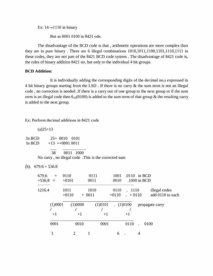
Ex: 14→1110 in binary
But as 0001 0100 in 8421 ode.
The disadvantage of the BCD code is that , arithmetic operations are more complex than
they are in pure binary . There are 6 illegal combinations 1010,1011,1100,1101,1110,1111 in
these codes, they are not part of the 8421 BCD code system . The disadvantage of 8421 code is,
the rules of binary addition 8421 no, but only to the individual 4 bit groups.
BCD Addition:
It is individually adding the corresponding digits of the decimal no,s expressed in
4 bit binary groups starting from the LSD . If there is no carry & the sum term is not an illegal
code , no correction is needed .If there is a carry out of one group to the next group or if the sum
term is an illegal code then 610(0100) is added to the sum term of that group & the resulting carry
is added to the next group.
Ex: Perform decimal additions in 8421 code
(a)25+13
In BCD 25= 0010 0101
In BCD +13 =+0001 0011
___ ___________
38 0011 1000
No carry , no illegal code .This is the corrected sum
(b). 679.6 + 536.8
679.6 = 0110 0111 1001 .0110 in BCD
+536.8 = +0101 0011 0010 .1000 in BCD _________ ___________________________________________________
1216.4 1011 1010 0110 . 1110 illegal codes
+0110 + 0011 +0110 . + 0110 add 0110 to each
_________________________________
(1)0001 (1)0000 (1)0101 . (1)0100 propagate carry
/ / / /
+1 +1 +1 +1
________________________________________
0001 0010 0001 0110 . 0100
1 2 1 6 . 4
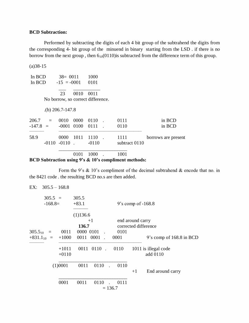
BCD Subtraction:
Performed by subtracting the digits of each 4 bit group of the subtrahend the digits from
the corresponding 4- bit group of the minuend in binary starting from the LSD . if there is no
borrow from the next group , then 610(0110)is subtracted from the difference term of this group.
(a)38-15
In BCD 38= 0011 1000
In BCD -15 = -0001 0101
___ ___________
23 0010 0011
No borrow, so correct difference.
.(b) 206.7-147.8
206.7 = 0010 0000 0110 . 0111 in BCD
-147.8 = -0001 0100 0111 . 0110 in BCD _________ ___________________________________________________
58.9 0000 1011 1110 . 1111 borrows are present
-0110 -0110 . -0110 subtract 0110
____________________________
0101 1000 . 1001
BCD Subtraction using 9’s & 10’s compliment methods:
Form the 9‘s & 10‘s compliment of the decimal subtrahend & encode that no. in
the 8421 code . the resulting BCD no.s are then added.
EX: 305.5 – 168.8
305.5 = 305.5
-168.8= +83.1 9‘s comp of -168.8
_________
(1)136.6
+1 end around carry
136.7 corrected difference
305.510 = 0011 0000 0101 . 0101
+831.110 = +1000 0011 0001 . 0001 9‘s comp of 168.8 in BCD _________ ___________________________________________________
+1011 0011 0110 . 0110 1011 is illegal code
+0110 add 0110
____________________________
(1)0001 0011 0110 . 0110
+1 End around carry
____________________________
0001 0011 0110 . 0111
= 136.7
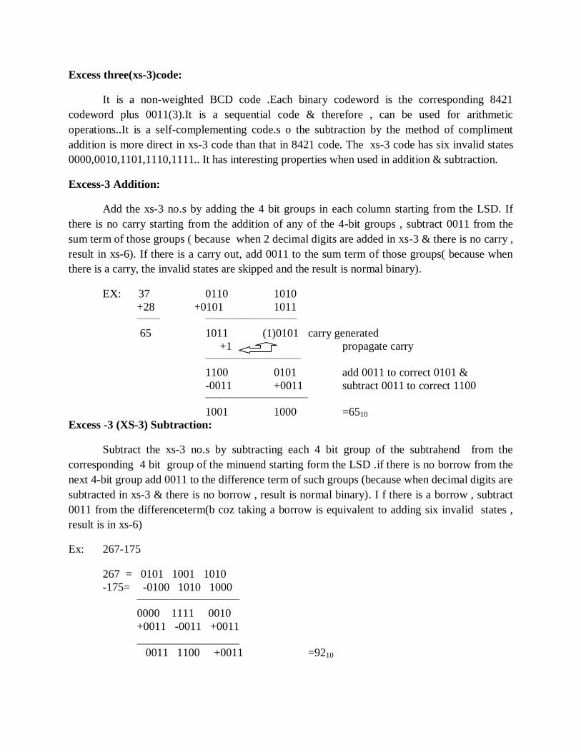
Excess three(xs-3)code:
It is a non-weighted BCD code .Each binary codeword is the corresponding 8421
codeword plus 0011(3).It is a sequential code & therefore , can be used for arithmetic
operations..It is a self-complementing code.s o the subtraction by the method of compliment
addition is more direct in xs-3 code than that in 8421 code. The xs-3 code has six invalid states
0000,0010,1101,1110,1111.. It has interesting properties when used in addition & subtraction.
Excess-3 Addition:
Add the xs-3 no.s by adding the 4 bit groups in each column starting from the LSD. If
there is no carry starting from the addition of any of the 4-bit groups , subtract 0011 from the
sum term of those groups ( because when 2 decimal digits are added in xs-3 & there is no carry ,
result in xs-6). If there is a carry out, add 0011 to the sum term of those groups( because when
there is a carry, the invalid states are skipped and the result is normal binary).
EX: 37 0110 1010
+28 +0101 1011 ______ ________________________
65 1011 (1)0101 carry generated
+1 propagate carry
_________________________
1100 0101 add 0011 to correct 0101 &
-0011 +0011 subtract 0011 to correct 1100
___________________________
1001 1000 =6510
Excess -3 (XS-3) Subtraction:
Subtract the xs-3 no.s by subtracting each 4 bit group of the subtrahend from the
corresponding 4 bit group of the minuend starting form the LSD .if there is no borrow from the
next 4-bit group add 0011 to the difference term of such groups (because when decimal digits are
subtracted in xs-3 & there is no borrow , result is normal binary). I f there is a borrow , subtract
0011 from the differenceterm(b coz taking a borrow is equivalent to adding six invalid states ,
result is in xs-6)
Ex: 267-175
267 = 0101 1001 1010
-175= -0100 1010 1000 ___________________________
0000 1111 0010
+0011 -0011 +0011
__________________
0011 1100 +0011 =9210
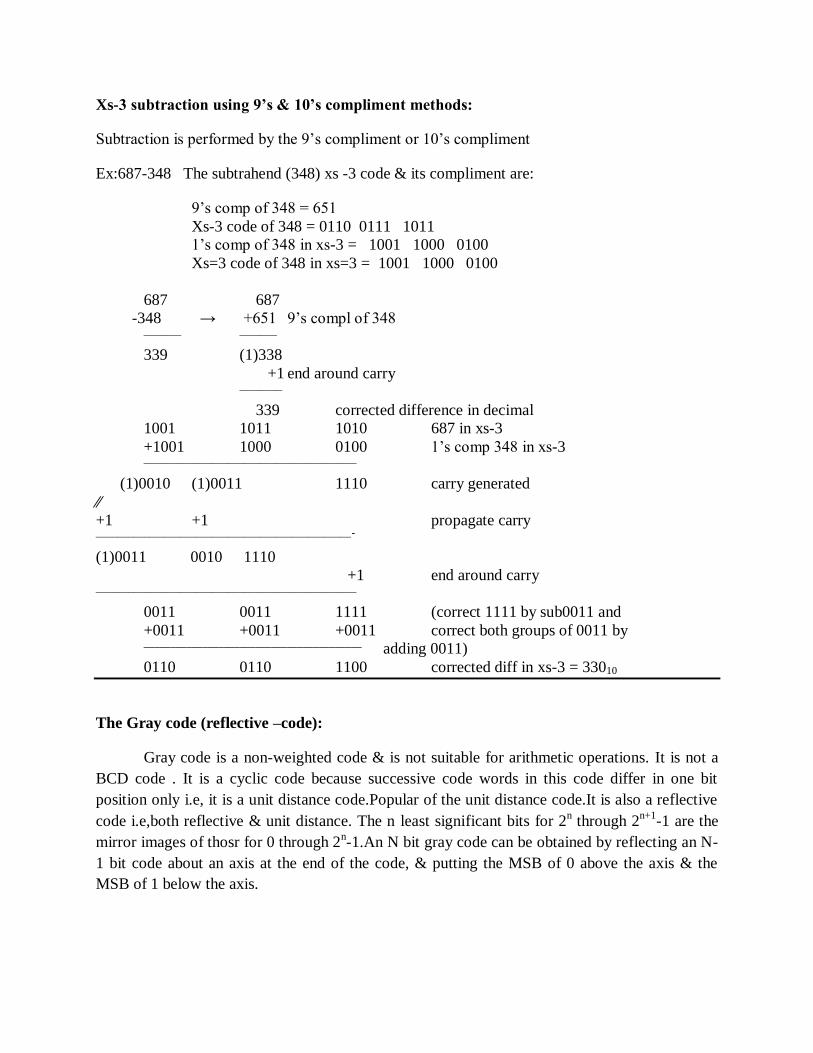
Xs-3 subtraction using 9’s & 10’s compliment methods:
Subtraction is performed by the 9‘s compliment or 10‘s compliment
Ex:687-348 The subtrahend (348) xs -3 code & its compliment are:
9‘s comp of 348 = 651
Xs-3 code of 348 = 0110 0111 1011
1‘s comp of 348 in xs-3 = 1001 1000 0100
Xs=3 code of 348 in xs=3 = 1001 1000 0100
687 687
-348 → +651 9‘s compl of 348
_______ _______
339 (1)338
+1 end around carry ________
339 corrected difference in decimal
1001 1011 1010 687 in xs-3
+1001 1000 0100 1‘s comp 348 in xs-3
________________________________________
(1)0010 (1)0011 1110 carry generated
⁄⁄
+1 +1
propagate carry
________________________________________________-
(1)0011 0010 1110
+1 end around carry _________________________________________________
0011 0011 1111 (correct 1111 by sub0011 and
+0011 +0011 +0011 correct both groups of 0011 by
_________________________________________
adding 0011)
0110 0110 1100 corrected diff in xs-3 = 33010
The Gray code (reflective –code):
Gray code is a non-weighted code & is not suitable for arithmetic operations. It is not a
BCD code . It is a cyclic code because successive code words in this code differ in one bit
position only i.e, it is a unit distance code.Popular of the unit distance code.It is also a reflective
code i.e,both reflective & unit distance. The n least significant bits for 2n through 2
n+1-1 are the
mirror images of thosr for 0 through 2n-1.An N bit gray code can be obtained by reflecting an N-
1 bit code about an axis at the end of the code, & putting the MSB of 0 above the axis & the
MSB of 1 below the axis.
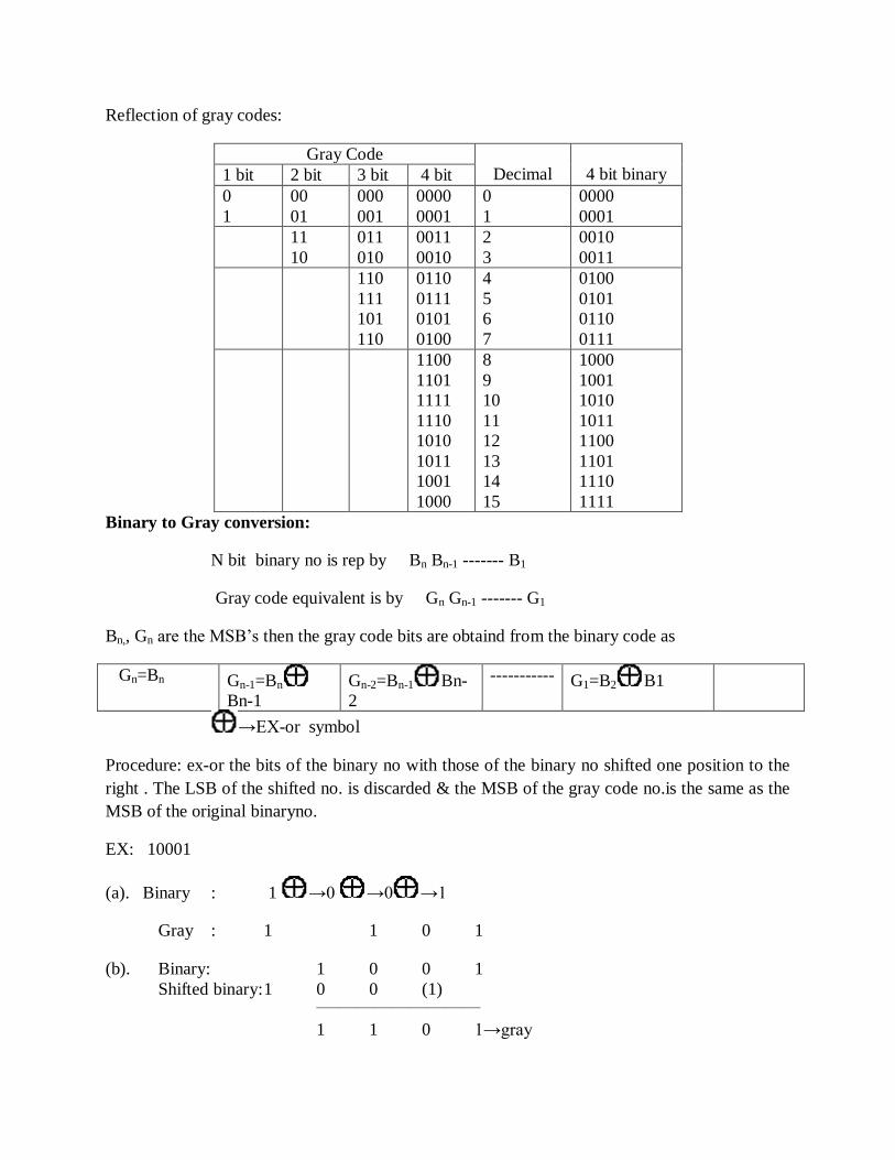
Reflection of gray codes:
Gray Code
Decimal
4 bit binary 1 bit 2 bit 3 bit 4 bit
0
1
00
01
000
001
0000
0001
0
1
0000
0001
11
10
011
010
0011
0010
2
3
0010
0011
110
111
101
110
0110
0111
0101
0100
4
5
6
7
0100
0101
0110
0111
1100
1101
1111
1110
1010
1011
1001
1000
8
9
10
11
12
13
14
15
1000
1001
1010
1011
1100
1101
1110
1111
Binary to Gray conversion:
N bit binary no is rep by Bn Bn-1 ------- B1
Gray code equivalent is by Gn Gn-1 ------- G1
Bn,, Gn are the MSB‘s then the gray code bits are obtaind from the binary code as
Gn=Bn Gn-1=Bn
Bn-1
Gn-2=Bn-1 Bn-
2
----------- G1=B2 B1
→EX-or symbol
Procedure: ex-or the bits of the binary no with those of the binary no shifted one position to the
right . The LSB of the shifted no. is discarded & the MSB of the gray code no.is the same as the
MSB of the original binaryno.
EX: 10001
(a). Binary : 1 →0 →0 →1
Gray : 1 1 0 1
(b). Binary: 1 0 0 1
Shifted binary: 1 0 0 (1)
____________________________
1 1 0 1→gray
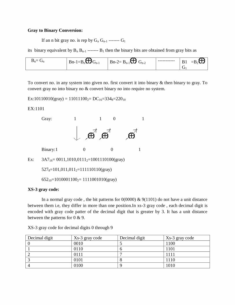
Gray to Binary Conversion:
If an n bit gray no. is rep by Gn Gn-1 ------- G1
its binary equivalent by Bn Bn-1 ------- B1 then the binary bits are obtained from gray bits as
Bn= Gn Bn-1=Bn Gn-1 Bn-2= Bn-1 Gn-2 ----------- B1 =B2
G1
To convert no. in any system into given no. first convert it into binary & then binary to gray. To
convert gray no into binary no & convert binary no into require no system.
Ex:10110010(gray) = 110111002= DC16=3348=22010
EX:1101
Gray: 1 1 0 1
Binary:1 0 0 1
Ex: 3A716= 0011,1010,01112=1001110100(gray)
5278=101,011,0112=111110110(gray)
65210=10100011002= 1111001010(gray)
XS-3 gray code:
In a normal gray code , the bit patterns for 0(0000) & 9(1101) do not have a unit distance
between them i.e, they differ in more than one position.In xs-3 gray code , each decimal digit is
encoded with gray code patter of the decimal digit that is greater by 3. It has a unit distance
between the patterns for 0 & 9.
XS-3 gray code for decimal digits 0 through 9
Decimal digit Xs-3 gray code Decimal digit Xs-3 gray code
0 0010 5 1100
1 0110 6 1101
2 0111 7 1111
3 0101 8 1110
4 0100 9 1010
Error – Detecting codes:When binary data is transmitted & processed,it is susceptible to noise
that can alter or distort its contents. The 1‘s may get changed to 0‘s & 1‘s .because digital
systems must be accurate to the digit, error can pose a problem. Several schemes have been
devised to detect the occurrence of a single bit error in a binary word, so that whenever such an
error occurs the concerned binary word can be corrected & retransmitted.
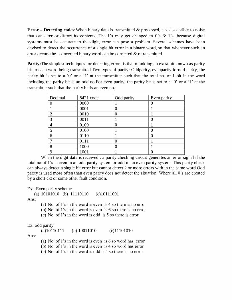
Parity:The simplest techniques for detecting errors is that of adding an extra bit known as parity
bit to each word being transmitted.Two types of parity: Oddparity, evenparity forodd parity, the
parity bit is set to a ‗0‘ or a ‗1‘ at the transmitter such that the total no. of 1 bit in the word
including the parity bit is an odd no.For even parity, the parity bit is set to a ‗0‘ or a ‗1‘ at the
transmitter such that the parity bit is an even no.
Decimal 8421 code Odd parity Even parity
0 0000 1 0
1 0001 0 1
2 0010 0 1
3 0011 1 0
4 0100 0 1
5 0100 1 0
6 0110 1 0
7 0111 0 1
8 1000 0 1
9 1001 1 0
When the digit data is received . a parity checking circuit generates an error signal if the
total no of 1‘s is even in an odd parity system or odd in an even parity system. This parity check
can always detect a single bit error but cannot detect 2 or more errors with in the same word.Odd
parity is used more often than even parity does not detect the situation. Where all 0‘s are created
by a short ckt or some other fault condition.
Ex: Even parity scheme
(a) 10101010 (b) 11110110 (c)10111001
Ans:
(a) No. of 1‘s in the word is even is 4 so there is no error
(b) No. of 1‘s in the word is even is 6 so there is no error
(c) No. of 1‘s in the word is odd is 5 so there is error
Ex: odd parity
(a)10110111 (b) 10011010 (c)11101010
Ans:
(a) No. of 1‘s in the word is even is 6 so word has error
(b) No. of 1‘s in the word is even is 4 so word has error
(c) No. of 1‘s in the word is odd is 5 so there is no error
Checksums:
Simple parity can‘t detect two errors within the same word. To overcome this, use a sort
of 2 dimensional parity. As each word is transmitted, it is added to the sum of the previously
transmitted words, and the sum retained at the transmitter end. At the end of transmission, the
sum called the check sum. Up to that time sent to the receiver. The receiver can check its sum
with the transmitted sum. If the two sums are the same, then no errors were detected at the
receiver end. If there is an error, the receiving location can ask for retransmission of the entire
data, used in teleprocessing systems.
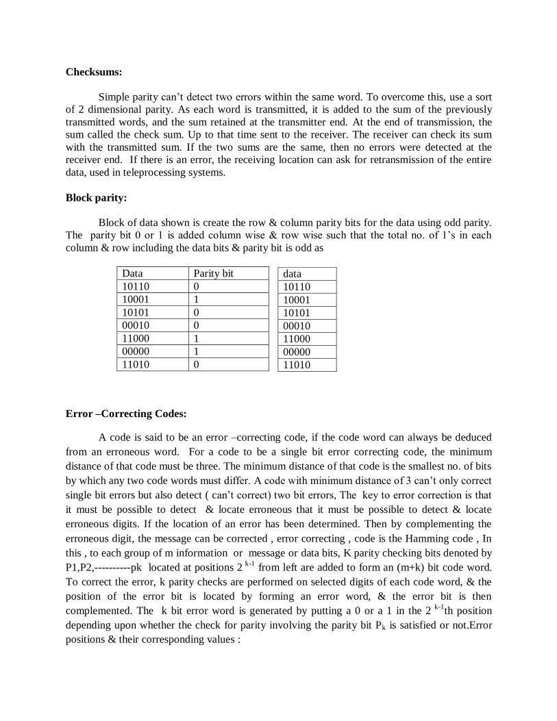
Block parity:
Block of data shown is create the row & column parity bits for the data using odd parity.
The parity bit 0 or 1 is added column wise & row wise such that the total no. of 1‘s in each
column & row including the data bits & parity bit is odd as
Data Parity bit
10110 0
10001 1
10101 0
00010 0
11000 1
00000 1
11010 0
Error –Correcting Codes:
A code is said to be an error –correcting code, if the code word can always be deduced
from an erroneous word. For a code to be a single bit error correcting code, the minimum
distance of that code must be three. The minimum distance of that code is the smallest no. of bits
by which any two code words must differ. A code with minimum distance of 3 can‘t only correct
single bit errors but also detect ( can‘t correct) two bit errors, The key to error correction is that
it must be possible to detect & locate erroneous that it must be possible to detect & locate
erroneous digits. If the location of an error has been determined. Then by complementing the
erroneous digit, the message can be corrected , error correcting , code is the Hamming code , In
this , to each group of m information or message or data bits, K parity checking bits denoted by
P1,P2,----------pk located at positions 2 k-1
from left are added to form an (m+k) bit code word.
To correct the error, k parity checks are performed on selected digits of each code word, & the
position of the error bit is located by forming an error word, & the error bit is then
complemented. The k bit error word is generated by putting a 0 or a 1 in the 2 k-1
th position
depending upon whether the check for parity involving the parity bit Pk is satisfied or not.Error
positions & their corresponding values :
data
10110
10001
10101
00010
11000
00000
11010
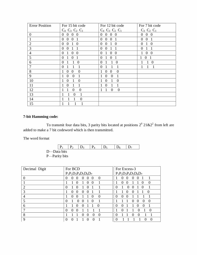
Error Position For 15 bit code
C4 C3 C2 C1
For 12 bit code
C4 C3 C2 C1
For 7 bit code
C3 C2 C1
0 0 0 0 0 0 0 0 0 0 0 0
1 0 0 0 1 0 0 0 1 0 0 1
2 0 0 1 0 0 0 1 0 0 1 0
3 0 0 1 1 0 0 1 1 0 1 1
4 0 1 0 0 0 1 0 0 1 0 0
5 0 1 0 1 0 1 0 1 1 0 1
6 0 1 1 0 0 1 1 0 1 1 0
7 0 1 1 1 0 1 1 1 1 1 1
8 1 0 0 0 1 0 0 0
9 1 0 0 1 1 0 0 1
10 1 0 1 0 1 0 1 0
11 1 0 1 1 1 0 1 1
12 1 1 0 0 1 1 0 0
13 1 1 0 1
14 1 1 1 0
15 1 1 1 1
7-bit Hamming code:
To transmit four data bits, 3 parity bits located at positions 20 21&2
2 from left are
added to make a 7 bit codeword which is then transmitted.
The word format
P1 P2 D3 P4 D5 D6 D7
D—Data bits
P—Parity bits
For Excess-3
P1P2D3P4D5D6D7
1 0 0 0 0 1 1
1 0 0 1 1 0 0
0 1 0 0 1 0 1
1 1 0 0 1 1 0
0 0 0 1 1 1 1
1 1 1 0 0 0 0
0 0 1 1 0 0 1
1 0 1 1 0 1 0
0 1 1 0 0 1 1
0 1 1 1 1 0 0
Decimal Digit For BCD
P1P2D3P4D5D6D7
0 0 0 0 0 0 0 0
1 1 1 0 1 0 0 1
2 0 1 0 1 0 1 1
3 1 0 0 0 0 1 1
4 1 0 0 1 1 0 0
5 0 1 0 0 1 0 1
6 1 1 0 0 1 1 0
7 0 0 0 1 1 1 1
8 1 1 1 0 0 0 0
9 0 0 1 1 0 0 1
Ex: Encode the data bits 1101 into the 7 bit even parity Hamming Code
The bit pattern is
P1P2D3P4D5D6D7
1 1 0 1
Bits 1,3,5,7 (P1 111) must have even parity, so P1 =1
Bits 2, 3, 6, 7(P2 101) must have even parity, so P2 =0
Bits 4,5,6,7 (P4 101)must have even parity, so P4 =0
The final code is 1010101
EX: Code word is 1001001
Bits 1,3,5,7 (C1 1001) →no error →put a 0 in the 1‘s position→C1=0
Bits 2, 3, 6, 7(C2 0001)) → error →put a 1 in the 2‘s position→C2=1
Bits 4,5,6,7 (C4 1001)) →no error →put a 0 in the 4‘s position→C3=0
15-bit Hamming Code: It transmit 11 data bits, 4 parity bits located 20 2
1 2
2 2
3
Word format is
P1 P2 D3 P4 D5 D6 D7 P8 D9 D10 D11 D12 D13 D14 D15
12-Bit Hamming Code:It transmit 8 data bits, 4 parity bits located at position 20 2
1 2
2 2
3
Word format is
P1 P2 D3 P4 D5 D6 D7 P8 D9 D10 D11 D12
Alphanumeric Codes:
These codes are used to encode the characteristics of alphabet in addition to the decimal
digits. It is used for transmitting data between computers & its I/O device such as printers,
keyboards & video display terminals.Popular modern alphanumeric codes are ASCII code &
EBCDIC code.
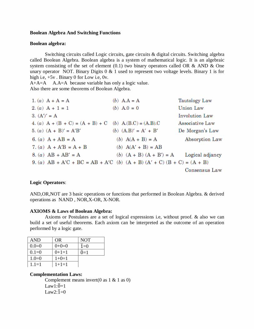
Boolean Algebra And Switching Functions
Boolean algebra:
Switching circuits called Logic circuits, gate circuits & digital circuits. Switching algebra
called Boolean Algebra. Boolean algebra is a system of mathematical logic. It is an algebraic
system consisting of the set of element (0.1) two binary operators called OR & AND & One
unary operator NOT. Binary Digits 0 & 1 used to represent two voltage levels. Binary 1 is for
high i.e, +5v . Binary 0 for Low i.e, 0v.
A+A=A A.A=A because variable has only a logic value.
Also there are some theorems of Boolean Algebra.
Logic Operators:
AND,OR,NOT are 3 basic operations or functions that performed in Boolean Algebra. & derived
operations as NAND , NOR,X-OR, X-NOR.
AXIOMS & Laws of Boolean Algebra:
Axioms or Postulates are a set of logical expressions i.e, without proof. & also we can
build a set of useful theorems. Each axiom can be interpreted as the outcome of an operation
performed by a logic gate.
Complementation Laws:
Complement means invert(0 as 1 & 1 as 0)
Law1:0 =1
Law2:1 =0
AND OR NOT
0.0=0 0+0=0 1 =0
0.1=0 0+1=1 0 =1
1.0=0 1+0=1
1.1=1 1+1=1
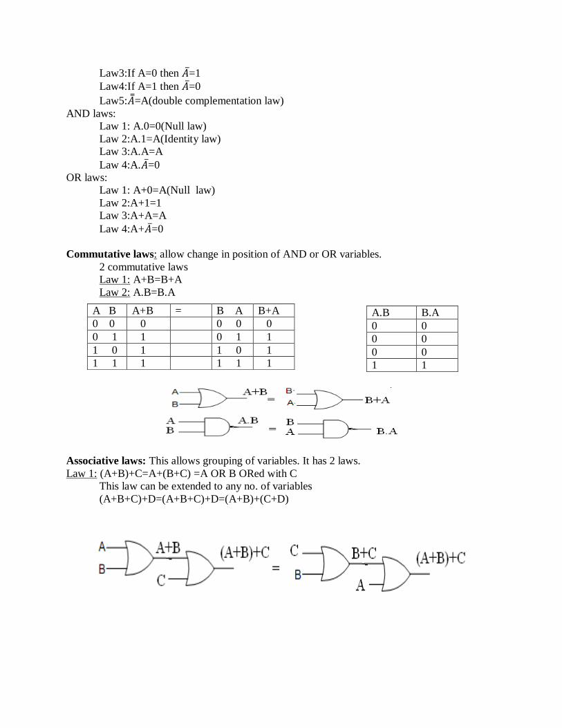
Law3:If A=0 then 𝐴 =1
Law4:If A=1 then 𝐴 =0
Law5:𝐴 =A(double complementation law)
AND laws:
Law 1: A.0=0(Null law)
Law 2:A.1=A(Identity law)
Law 3:A.A=A
Law 4:A.𝐴 =0
OR laws:
Law 1: A+0=A(Null law)
Law 2:A+1=1
Law 3:A+A=A
Law 4:A+𝐴 =0
Commutative laws: allow change in position of AND or OR variables.
2 commutative laws
Law 1: A+B=B+A
Law 2: A.B=B.A
Associative laws: This allows grouping of variables. It has 2 laws.
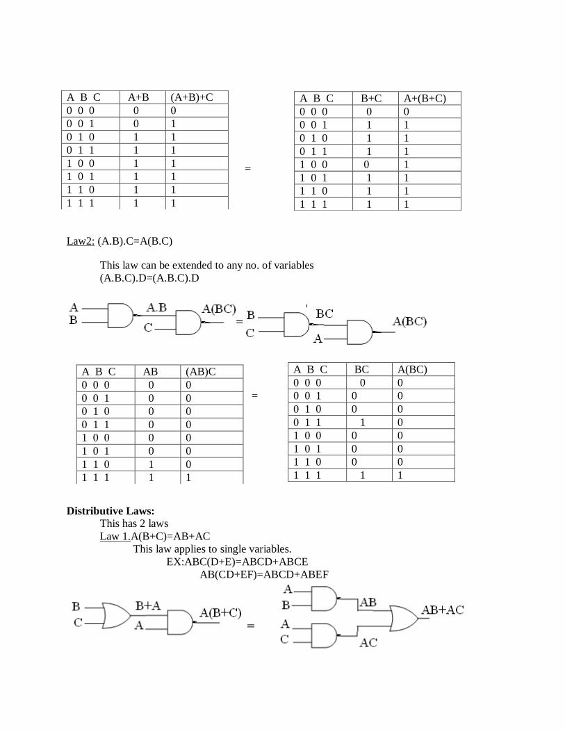
Law 1: (A+B)+C=A+(B+C) =A OR B ORed with C
This law can be extended to any no. of variables
(A+B+C)+D=(A+B+C)+D=(A+B)+(C+D)
A.B B.A
0 0
0 0
0 0
1 1
A B A+B = B A B+A
0 0 0 0 0 0
0 1 1 0 1 1
1 0 1 1 0 1
1 1 1 1 1 1
=
Law2: (A.B).C=A(B.C)
This law can be extended to any no. of variables
(A.B.C).D=(A.B.C).D
=
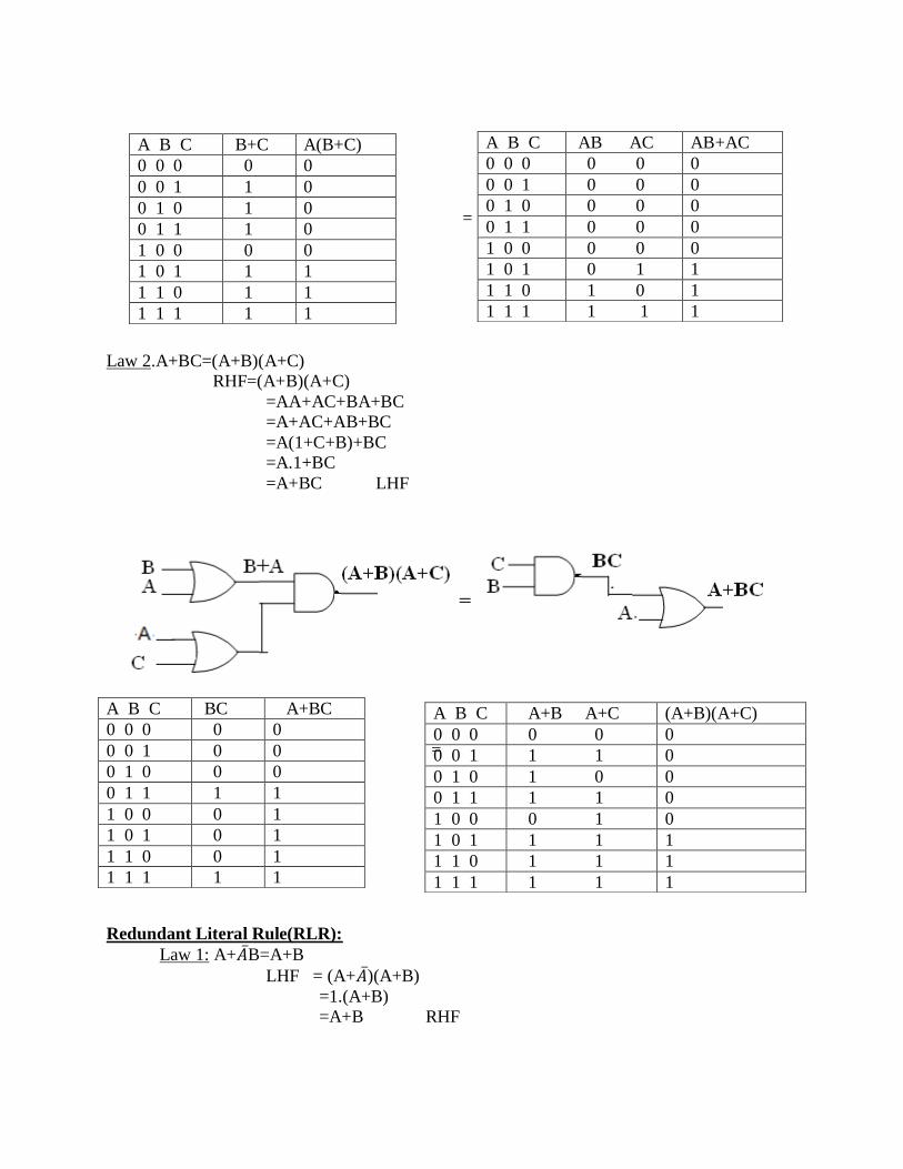
Distributive Laws:
This has 2 laws
Law 1.A(B+C)=AB+AC
This law applies to single variables.
EX:ABC(D+E)=ABCD+ABCE
AB(CD+EF)=ABCD+ABEF
A B C A+B (A+B)+C
0 0 0 0 0
0 0 1 0 1
0 1 0 1 1
0 1 1 1 1
1 0 0 1 1
1 0 1 1 1
1 1 0 1 1
1 1 1 1 1
A B C B+C A+(B+C)
0 0 0 0 0
0 0 1 1 1
0 1 0 1 1
0 1 1 1 1
1 0 0 0 1
1 0 1 1 1
1 1 0 1 1
1 1 1 1 1
A B C BC A(BC)
0 0 0 0 0
0 0 1 0 0
0 1 0 0 0
0 1 1 1 0
1 0 0 0 0
1 0 1 0 0
1 1 0 0 0
1 1 1 1 1
A B C AB (AB)C
0 0 0 0 0
0 0 1 0 0
0 1 0 0 0
0 1 1 0 0
1 0 0 0 0
1 0 1 0 0
1 1 0 1 0
1 1 1 1 1
=
Law 2.A+BC=(A+B)(A+C)
RHF=(A+B)(A+C)
=AA+AC+BA+BC
=A+AC+AB+BC
=A(1+C+B)+BC
=A.1+BC
=A+BC LHF
=
Redundant Literal Rule(RLR):
Law 1: A+𝐴 B=A+B
LHF = (A+𝐴 )(A+B)
=1.(A+B)
=A+B RHF
A B C AB AC AB+AC
0 0 0 0 0 0
0 0 1 0 0 0
0 1 0 0 0 0
0 1 1 0 0 0
1 0 0 0 0 0
1 0 1 0 1 1
1 1 0 1 0 1
1 1 1 1 1 1
A B C B+C A(B+C)
0 0 0 0 0
0 0 1 1 0
0 1 0 1 0
0 1 1 1 0
1 0 0 0 0
1 0 1 1 1
1 1 0 1 1
1 1 1 1 1
A B C BC A+BC
0 0 0 0 0
0 0 1 0 0
0 1 0 0 0
0 1 1 1 1
1 0 0 0 1
1 0 1 0 1
1 1 0 0 1
1 1 1 1 1
A B C A+B A+C (A+B)(A+C)
0 0 0 0 0 0
0 0 1 1 1 0
0 1 0 1 0 0
0 1 1 1 1 0
1 0 0 0 1 0
1 0 1 1 1 1
1 1 0 1 1 1
1 1 1 1 1 1
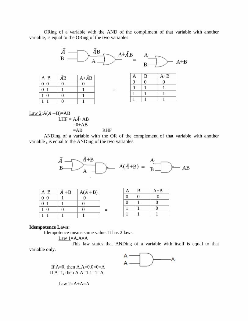
ORing of a variable with the AND of the compliment of that variable with another
variable, is equal to the ORing of the two variables.
=
Law 2:A(𝐴 +B)=AB
LHF = A𝐴 +AB
=0+AB
=AB RHF
ANDing of a variable with the OR of the complement of that variable with another
variable , is equal to the ANDing of the two variables.
=
Idempotence Laws:
Idempotence means same value. It has 2 laws.
Law 1=A.A=A
This law states that ANDing of a variable with itself is equal to that
variable only.
If A=0, then A.A=0.0=0=A
If A=1, then A.A=1.1=1=A
Law 2=A+A=A
A B 𝐴 B A+𝐴 B
0 0 0 0
0 1 1 1
1 0 0 1
1 1 0 1
A B A+B
0 0 0
0 1 1
1 1 1
1 1 1
A B 𝐴 +B A(𝐴 +B)
0 0 1 0
0 1 1 0
1 0 0 0
1 1 1 1
A B A+B
0 0 0
0 1 0
1 1 0
1 1 1
This law states that ORing of a variable with itself is equal to that
variable only.
If A=0, then A+A=0+0=0=A
If A=1, then A+A=1+1=1=A
Absorption Laws:
Law 1=A+A.B=A
= A(1+B)
=A.1
=A
i.e., A+A. any term=A
Law 2=A(A+B)=A
A(A+B)=A.A+A.B
= A+AB
=A(1+B)
= A.1
=A
Consensus theorem:
Theorem 1: AB+𝐴 C+BC=AB+𝐴 c
LHS: AB+𝐴 C+BC
=AB+𝐴 C+BC(A+𝐴 ) =AB+𝐴 C+BCA+BC𝐴 =AB(1+C)+𝐴 c(1)
=AB+𝐴 C
RHS
A B 𝐴𝐵 A+𝐴B)
0 0 0 0
0 1 0 0
1 0 0 1
1 1 1 1
A B 𝐴 + 𝐵 A(A+B)
0 0 0 0
0 1 1 0
1 0 1 1
1 1 1 1
This can be extended to any no. of variables
EX: AB+𝐴 C+BCD =AB+𝐴 𝐶
Theorem 2: (A+B)(𝐴 + 𝐶)(B+C)=(A+B)(𝐴 +C)
Transposition Theorem:
AB+𝐴 C= (A+C)(𝐴 +B)
RHS: (A+C)(𝐴 +B)
=A𝐴 +C𝐴 +AB+CB
=0+𝐴 C+AB+BC
=𝐴 C+AB+BC(A+𝐴 ) =AB+ABC+𝐴 C+𝐴 BC
=AB+𝐴 C
LHS
DeMorgans Theorem:
It represents two of the most powerful laws in Boolean algebra
Law 1: 𝐴 + 𝐵 =𝐴 𝐵
This law states that the compliment of a sum of variables is equal to the product
of their individual complements.
LHS
RHS
NOR gate Bubbled AND gate
A B A+B (A+B)‘
0 0 0 1
0 1 1 0
1 0 1 0
1 1 1 0
A B A‘ B‘ A‘B‘
0 0 1 1 1
0 1 1 0 0
1 0 0 1 0
1 1 0 0 0
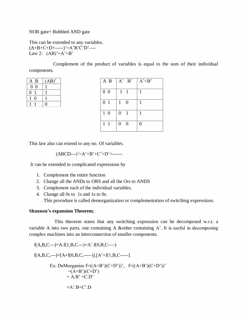
NOR gate= Bubbled AND gate
This can be extended to any variables.
(A+B+C+D+-----)‘=A‘B‘C‘D‘----
Law 2: (AB)‘=A‘+B‘
Complement of the product of variables is equal to the sum of their individual
components.
This law also can extend to any no. Of variables.
(ABCD---)‘=A‘+B‘+C‘+D‘+------
It can be extended to complicated expressions by
1. Complement the entire function
2. Change all the ANDs to ORS and all the Ors to ANDS
3. Complement each of the individual variables.
4. Change all 0s to 1s and 1s to 0s.
This procedure is called demorganization or complementation of switching expressions.
Shannon’s expansion Theorem:
This theorem states that any switching expression can be decomposed w.r.t. a
variable A into two parts, one containing A &other containing A‘. It is useful in decomposing
complex machines into an interconnection of smaller components.
f(A,B,C---)=A.f(1,B,C---)+A‘.f(0,B,C----)
f(A,B,C,---)=[A+f(0,B,C,-----)].[A‘+f(1,B,C-----]
Ex: DeMorganize f=((A+B‘)(C+D‘))‘, f=((A+B‘)(C+D‘))‘
=(A+B‘)(C+D‘) = A.B‘ +C.D‘
=A‘.B+C‘.D
A B (AB)‘
0 0 1
0 1 1
1 0 1
1 1 0
A B A‘ B‘ A‘+B‘
0 0 1 1 1
0 1 1 0 1
1 0 0 1 1
1 1 0 0 0
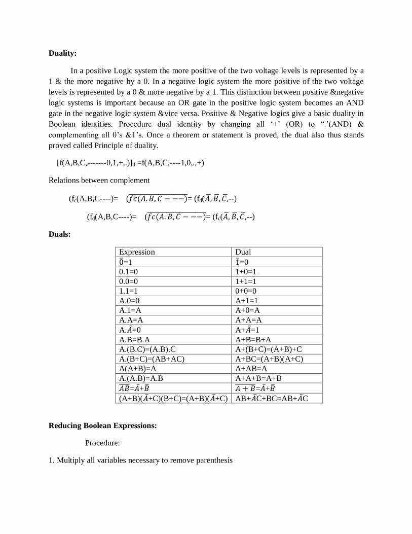
Duality:
In a positive Logic system the more positive of the two voltage levels is represented by a
1 & the more negative by a 0. In a negative logic system the more positive of the two voltage
levels is represented by a 0 & more negative by a 1. This distinction between positive &negative
logic systems is important because an OR gate in the positive logic system becomes an AND
gate in the negative logic system &vice versa. Positive & Negative logics give a basic duality in
Boolean identities. Procedure dual identity by changing all ‗+‘ (OR) to ―.‘(AND) &
complementing all 0‘s &1‘s. Once a theorem or statement is proved, the dual also thus stands
proved called Principle of duality.
[f(A,B,C,-------0,1,+,.)]d =f(A,B,C,----1,0,.,+)
Relations between complement
(fc(A,B,C----)= (𝑓𝑐(𝐴.𝐵, 𝐶 − −−) = (fd(𝐴, 𝐵, 𝐶, --)
(fd(A,B,C----)= (𝑓𝑐(𝐴. 𝐵,𝐶 − −−) = (fc(𝐴, 𝐵, 𝐶, --)
Duals:
Expression Dual
0 =1 1 =0
0.1=0 1+0=1
0.0=0 1+1=1
1.1=1 0+0=0
A.0=0 A+1=1
A.1=A A+0=A
A.A=A A+A=A
A.𝐴 =0 A+𝐴 =1
A.B=B.A A+B=B+A
A.(B.C)=(A.B).C A+(B+C)=(A+B)+C
A.(B+C)=(AB+AC) A+BC=(A+B)(A+C)
A(A+B)=A A+AB=A
A.(A.B)=A.B A+A+B=A+B
𝐴𝐵 =𝐴 +𝐵 𝐴 + 𝐵 =𝐴 +𝐵
(A+B)(𝐴 +C)(B+C)=(A+B)(𝐴 +C) AB+𝐴 C+BC=AB+𝐴 C
Reducing Boolean Expressions:
Procedure:
1. Multiply all variables necessary to remove parenthesis
2. Look for identical terms. Only one of those terms to be retained & other
dropped.
Ex: AB+AB+AB+AB=AB
4. Look for a variable & its negation in the same term. This term can be dropped 1
Ex: AB𝐶 𝐷 +AB𝐶 = AB𝐶 (𝐷 +1)=AB𝐶 .1=AB𝐶
5. Look for pairs of terms which have the same variables,with one or more variables
complemented. If a variable in one term of such a pair is complemented while in the
second term it is not then such terms can be combined into a single term with variable
dropped.
Ex: AB𝐶 𝐷 +AB𝐶 D= AB𝐶 (𝐷 +D)=AB𝐶 .1=AB𝐶 unctions
Boolean functions & their representation:
A function of n Boolean variables denoted by f(x1,x2,x3------xn) is another variable
denoted by & takes one of the two possible values 0 & 1.
The various way of represent a given function is
1. Sum of Product(SOP) form:
It is called the Disjunctive Normal Form(DNF)
Ex:f(A,B,C)=(𝐴 B+𝐵 C)
2. Product of Sums (POS) form:
It is called the Conjunctive Normal Form(CNF).This is implemented usin Consensus
theorem.
Ex:f(A,B,C)=(𝐴 + B)(B+C)
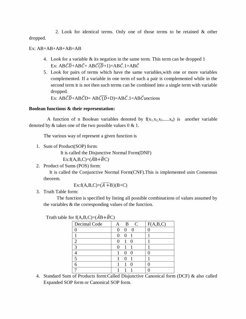
3. Truth Table form:
The function is specified by listing all possible combinations of values assumed by
the variables & the corresponding values of the function.
Truth table for f(A,B,C)=(𝐴 B+𝐵 C)
Decimal Code A B C F(A,B,C)
0 0 0 0 0
1 0 0 1 1
2 0 1 0 1
3 0 1 1 1
4 1 0 0 0
5 1 0 1 1
6 1 1 0 0
7 1 1 1 0
4. Standard Sum of Products form:Called Disjunctive Canonical form (DCF) & also called
Expanded SOP form or Canonical SOP form.
f(A,B,C)=(𝐴 B+𝐵 C)=𝐴 B(C+𝐶 )+𝐵 C(A+𝐴 )
=𝐴 𝐵 C+𝐴 B𝐶 +𝐴 BC+A𝐵 C
A Product term contains all the variables of the function either in complemented or
Uncomplemented form is called a minterm. A minterm assumes the value 1 only for one
combination of the variables. An n variable function can have in all 2n
minterms to 1 is
the standard sum of products form of the function. Min terms are denoted as m0, m1,m2--
--. Here suffixes are denoted by the decimal codes.
Ex: 3 variable functions
m0=𝐴 𝐵 𝐶
m1=𝐴 𝐵 C
m2=𝐴 B𝐶
m3=𝐴 BC
׀
= CBA 7 m no other way of representation in canonical SOP form is , the SUM
of minterms for which the function equals 1.Thus
f(A,B,C)=m1+m2+m3+m5
The function in DCF is listing the decimal codes of the minterms for which f=1
f(A,B,C)=∑m(1,2,3,5).
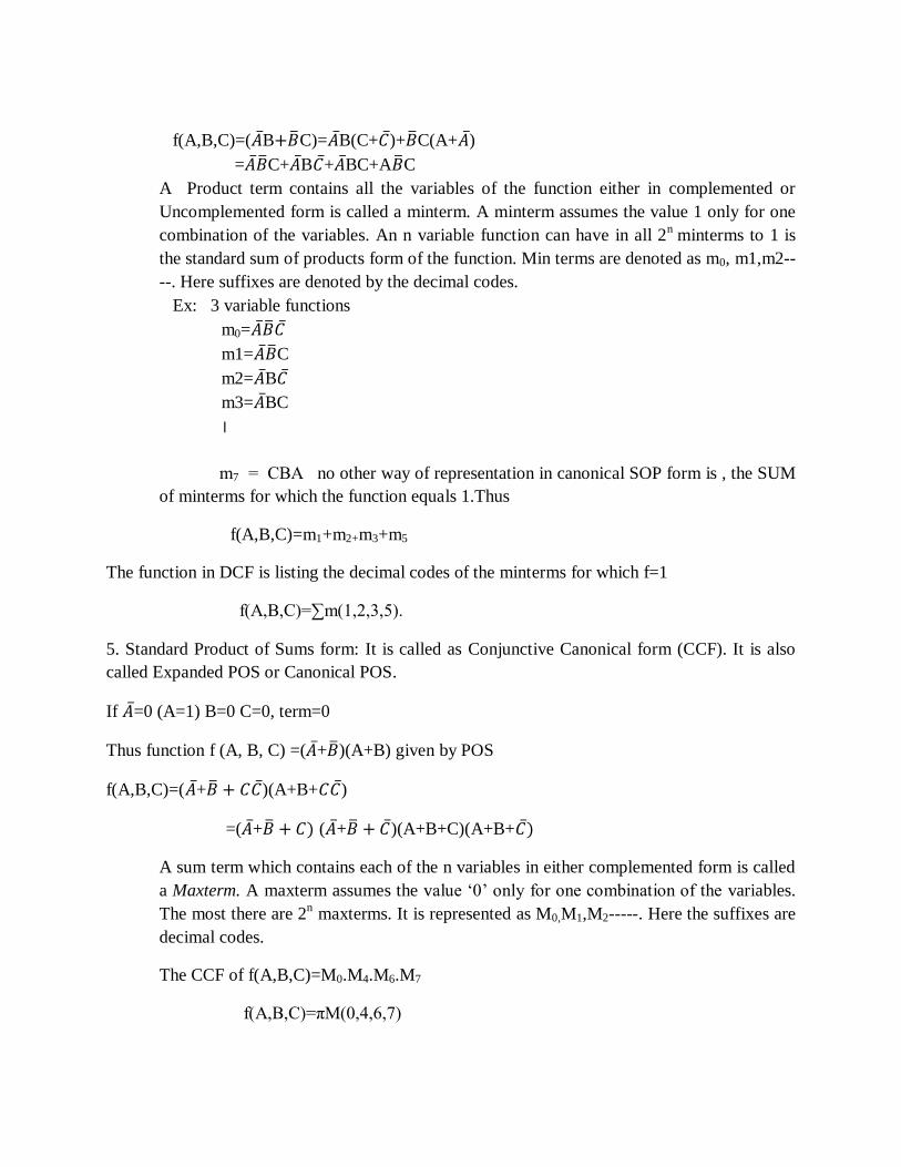
5. Standard Product of Sums form: It is called as Conjunctive Canonical form (CCF). It is also
called Expanded POS or Canonical POS.
If 𝐴 =0 (A=1) B=0 C=0, term=0
Thus function f (A, B, C) =(𝐴 +𝐵 )(A+B) given by POS
f(A,B,C)=(𝐴 +𝐵 + 𝐶𝐶 )(A+B+𝐶𝐶 )
=(𝐴 +𝐵 + 𝐶) (𝐴 +𝐵 + 𝐶 )(A+B+C)(A+B+𝐶 )
A sum term which contains each of the n variables in either complemented form is called
a Maxterm. A maxterm assumes the value ‗0‘ only for one combination of the variables.
The most there are 2n maxterms. It is represented as M0,M1,M2-----. Here the suffixes are
decimal codes.
The CCF of f(A,B,C)=M0.M4.M6.M7
f(A,B,C)=πM(0,4,6,7)
π or ^ represents the product of all maxterms.
6. Octal designation:
m7m6 m5 m4 m3 m2 m1 m0
0 0 1 0 1 1 1 0
7. Karnaugh Map:
Put the Truth Table in a compact form by labeling the row & columns of a map. It
is used in the minimization of functions 3,4,5,6 variables.
m0,m1,m2 ----- are minterms
M0,M1,M2,M3-------- are Maxterms.
Expansion of a Boolean expression in SOP form to the standard SOP form:
1.Write down all the terms.
2. If one or more variables are missing in any term.Expand that term by multiplying it with
the sum of each one of the missing variable and its complement.
3. Drop out redundant terms.
* interms of minterms:
1.Write down all the
terms.
2.Put Xs in terms where variables must be inserted to form a minterm.
3.Replace the non-complemented variables by 1s and the complemented variables by 0s,
and use all combinations of Xs in terms of 0s and 1s to generate minterms.
4. Drop out redundant terms.
Expansion of a Boolean expression in POS form to standard POS form:
1. Write down all the terms.
2. . If one or more variables are missing in any sum term. expand that term by adding the
product of each of the missing variable and its complement.
3. Drop out redundant terms.
Interms of Maxterms:
1. Write down all the terms.
2. Put x‘s in terms where variable inserted
3. Replace complemented variable by 1‘s & non complemented variable by 0‘s.& use
all combinations.
4. Drop out redundant terms.
Conversion between Canonical form:
The complement of a function expressed as the sum of minterms equals the sum of
minterms missing from the original function is expressed by those minterms that make
the function equal to 1 for those minterms that make the function equal to 0.
Ex: f(A,B,C)=πm(0,2,4,6,7)
Complement is
𝑓(𝐴,𝐵,𝐶 =∑m(1,3,5).=m1+m3+m5
complement of 𝑓 by deMorgans theorem
f= (m1 + m3 + m5) =𝑚1 .𝑚2 .𝑚5 =M1 M3 M5=πM(1,3,5)
𝑚1 =Mj , the maxterm with subscript j is a complement of the minterm with the same
subscript j and vice versa. To convert one canonical form to another, interchange the
symbol ∑ and π, and list those numbers missing from the original form.
Computation of total gate inputs:
The total number of gate inputs required to realize a Boolean expression is
computed as, If the expression is in the SOP form, count the number of AND inputs and
number of AND gates feeding the OR gate. If the expression is in the POS form, count
the number of OR inputs and the number of OR gates feeding the AND gate. If it is in
hybrid form, count the gate inputs and the gates feeding other gates. The cost of
implementing circuit is proportional to no. of gate inputs required.
EX: ABC+A𝐵 CD +E𝐹 +AD
1. Count the AND Inputs 3+4+2+2=11
2. Count AND gates feeding the OR gate 1+1+1+1=4
3. Total gate inputs =15
Boolean Expression & Logic Diagrams:
Boolean expressions can be realized as hardware using logic gates.
Conversely, hardware can be translated into Boolean expressions for the analysis of
existing circuits.
1. Converting Boolean Expressions to Logic:
To convert, start with the output & work towards the input.
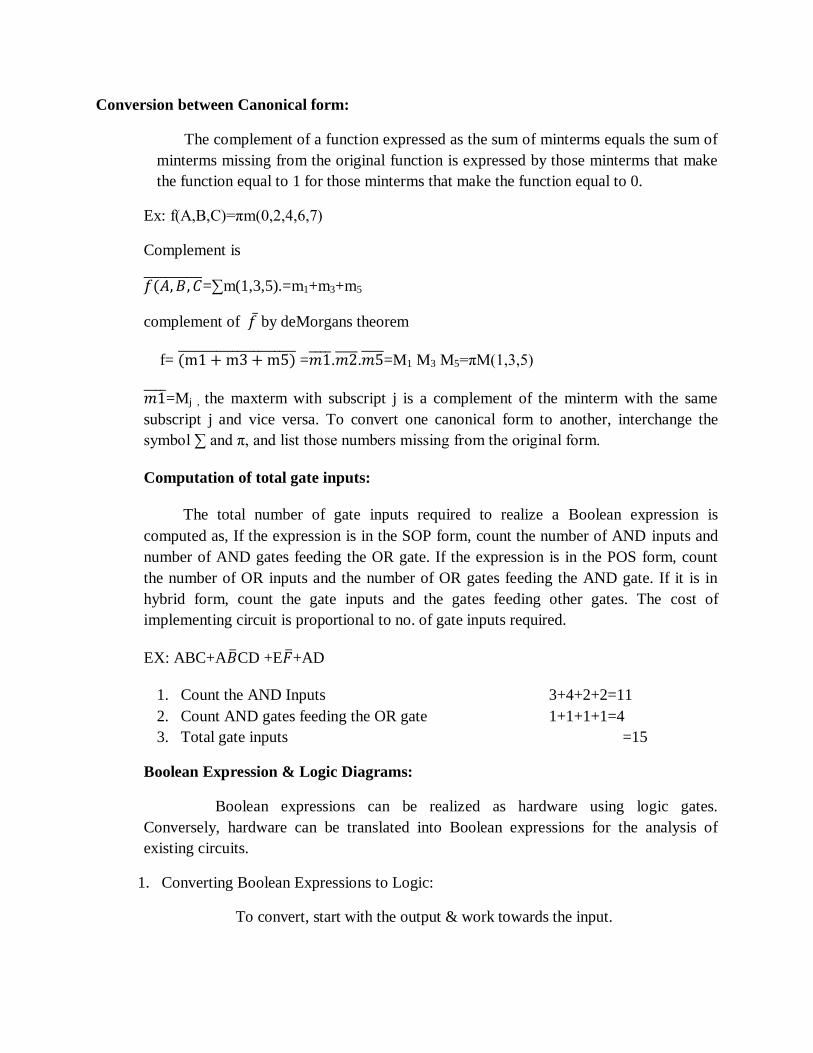
Assume the expression 𝐴𝐵 +A+𝐵 + 𝐶 is to be realized using AOI logic. Start
with this expression. Since it is three terms, it must be the output of a three-input OR
gates. So, draw an OR gate with three inputs as
(AB)‘ is the output of an inverter whose inputs is AB and (B+C)‘ must be the output of
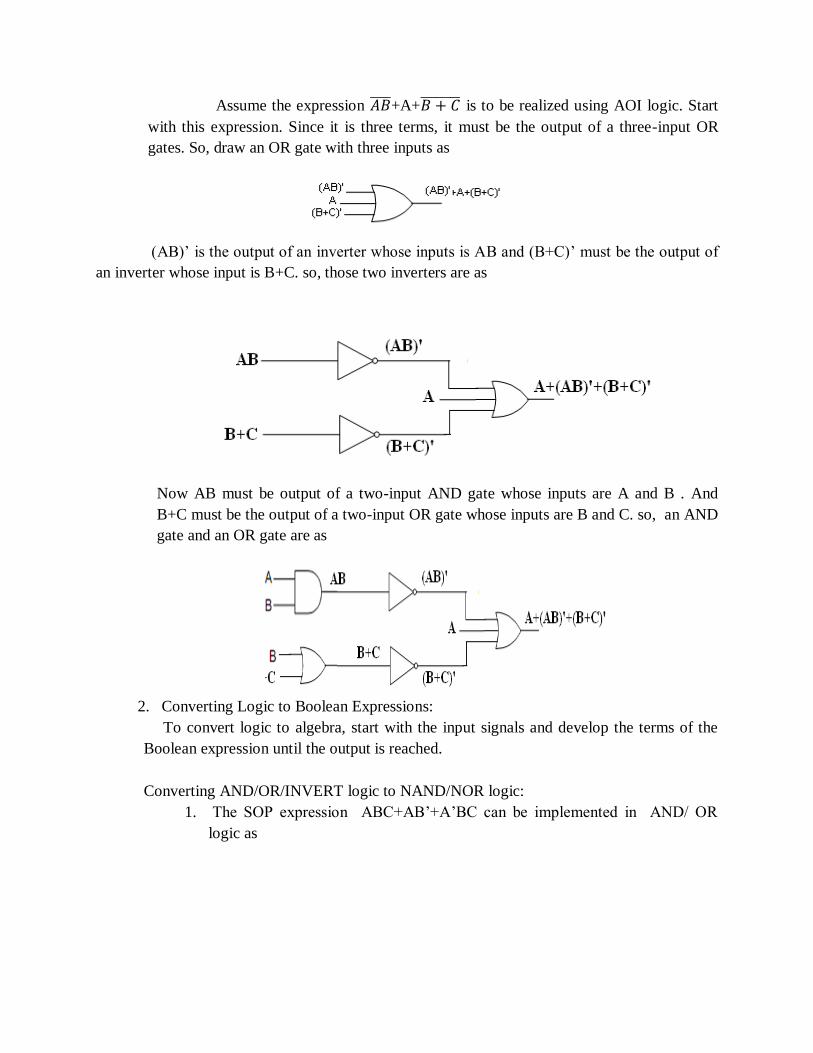
an inverter whose input is B+C. so, those two inverters are as
Now AB must be output of a two-input AND gate whose inputs are A and B . And
B+C must be the output of a two-input OR gate whose inputs are B and C. so, an AND
gate and an OR gate are as
2. Converting Logic to Boolean Expressions:
To convert logic to algebra, start with the input signals and develop the terms of the
Boolean expression until the output is reached.
Converting AND/OR/INVERT logic to NAND/NOR logic:
1. The SOP expression ABC+AB‘+A‘BC can be implemented in AND/ OR
logic as
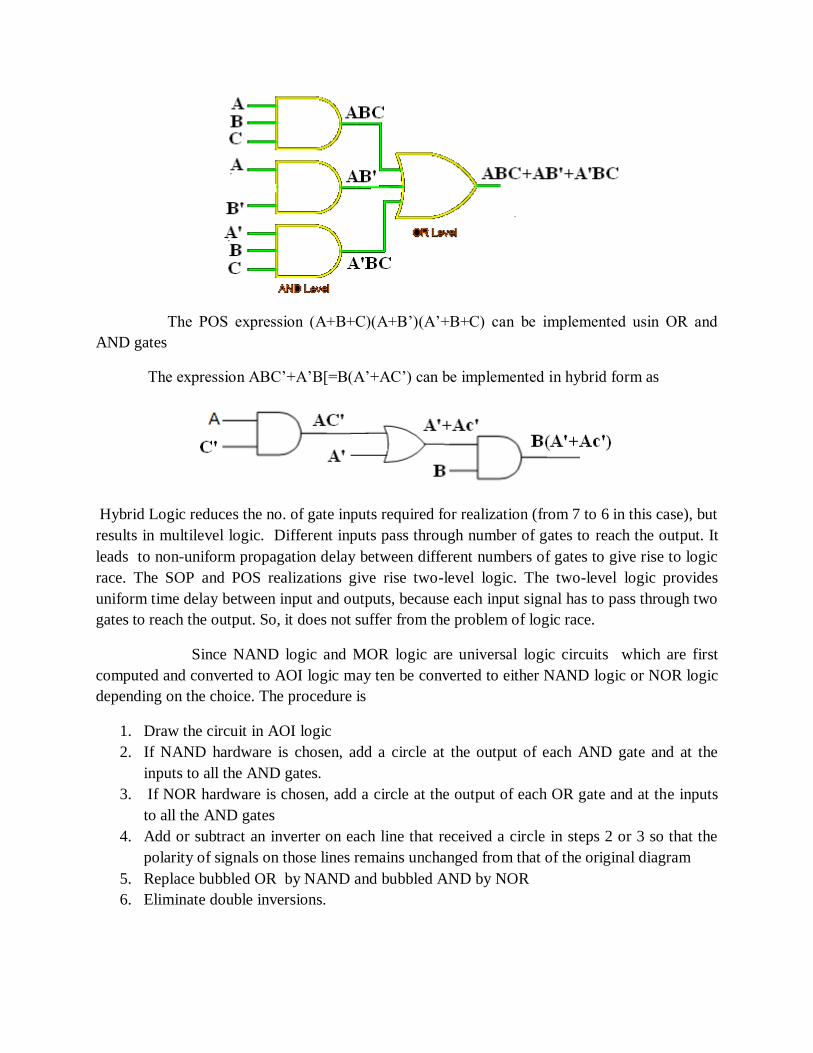
The POS expression (A+B+C)(A+B‘)(A‘+B+C) can be implemented usin OR and
AND gates
The expression ABC‘+A‘B[=B(A‘+AC‘) can be implemented in hybrid form as
Hybrid Logic reduces the no. of gate inputs required for realization (from 7 to 6 in this case), but
results in multilevel logic. Different inputs pass through number of gates to reach the output. It
leads to non-uniform propagation delay between different numbers of gates to give rise to logic
race. The SOP and POS realizations give rise two-level logic. The two-level logic provides
uniform time delay between input and outputs, because each input signal has to pass through two
gates to reach the output. So, it does not suffer from the problem of logic race.
Since NAND logic and MOR logic are universal logic circuits which are first
computed and converted to AOI logic may ten be converted to either NAND logic or NOR logic
depending on the choice. The procedure is
1. Draw the circuit in AOI logic
2. If NAND hardware is chosen, add a circle at the output of each AND gate and at the
inputs to all the AND gates.
3. If NOR hardware is chosen, add a circle at the output of each OR gate and at the inputs
to all the AND gates
4. Add or subtract an inverter on each line that received a circle in steps 2 or 3 so that the
polarity of signals on those lines remains unchanged from that of the original diagram
5. Replace bubbled OR by NAND and bubbled AND by NOR
6. Eliminate double inversions.
LOGIC GATES: Logic gates are fundamental building blocks of digital systems. Logic gate
produces one output level when some combinations of input levels are present. & a different
output level when other combination of input levels is present. In this, 3 basic types of gates are
there. AND OR & NOT
The interconnection of gates to perform a variety of logical operation is called Logic
Design. Inputs & outputs of logic gates can occur only in two levels.1,0 or High, Low or True ,
False or On , Off. A table which lists all the possible combinations of input variables & the
corresponding outputs is called a Truth Table. It shows how the logic circuits output responds to
various combinations of logic levels at the inputs. Level Logic, a logic in which the voltage levels
represent logic 1 & logic 0.Level logic may be Positive Logic or Negative Logic. In Positive
Logic the higher of two voltage levels represent logic 1 & Lower of two voltage levels represent
logic 0.In Negative Logic the lower of two voltage levels represent logic 1 & higher of two
voltage levels represent logic 0.
In TTl (Transistor-Transistor Logic) Logic family voltage levels are +5v, 0v.Logic 1 represent
+5v & Logic 0 represent 0v.
AND Gate:
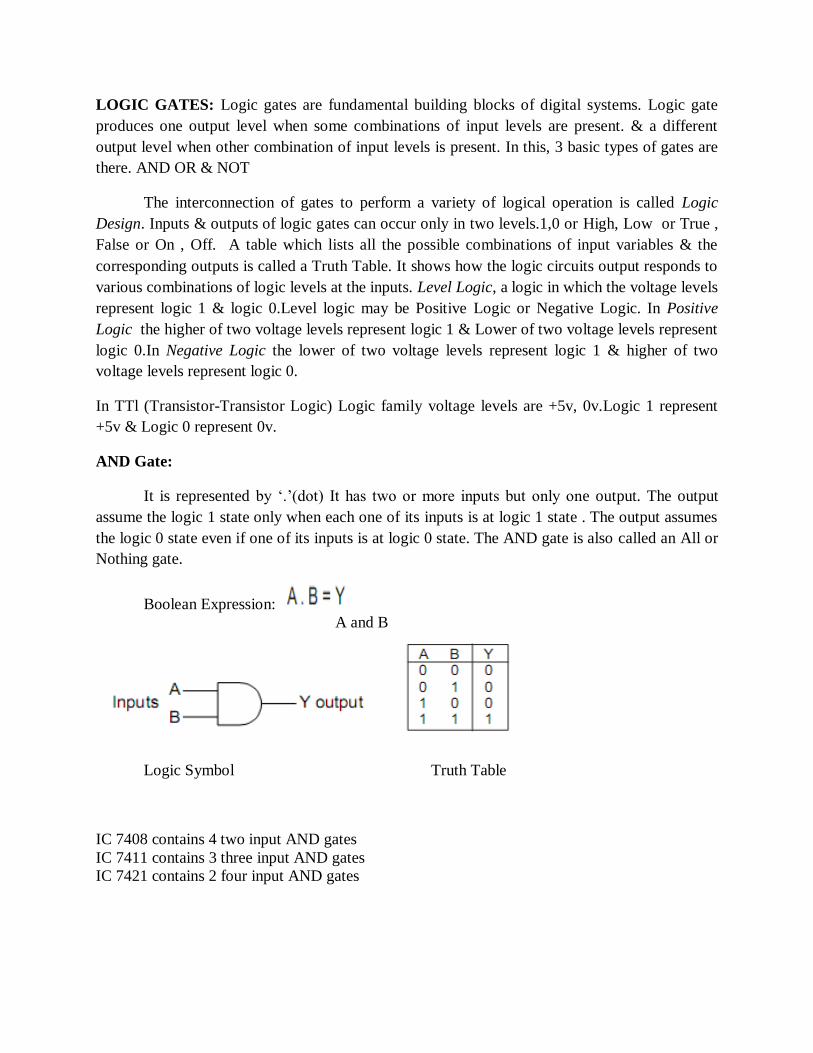
It is represented by ‗.‘(dot) It has two or more inputs but only one output. The output
assume the logic 1 state only when each one of its inputs is at logic 1 state . The output assumes
the logic 0 state even if one of its inputs is at logic 0 state. The AND gate is also called an All or
Nothing gate.
Boolean Expression:
A and B
Logic Symbol Truth Table
IC 7408 contains 4 two input AND gates
IC 7411 contains 3 three input AND gates
IC 7421 contains 2 four input AND gates
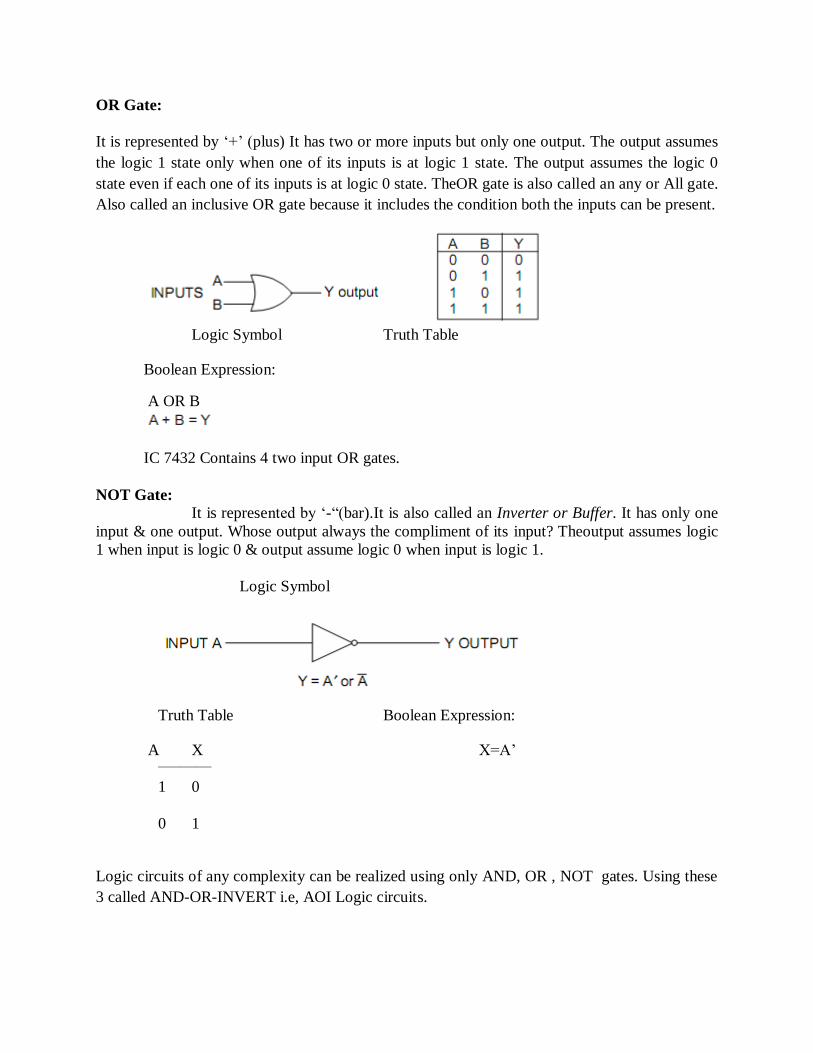
OR Gate:
It is represented by ‗+‘ (plus) It has two or more inputs but only one output. The output assumes
the logic 1 state only when one of its inputs is at logic 1 state. The output assumes the logic 0
state even if each one of its inputs is at logic 0 state. TheOR gate is also called an any or All gate.
Also called an inclusive OR gate because it includes the condition both the inputs can be present.
Logic Symbol Truth Table
Boolean Expression:
A OR B
IC 7432 Contains 4 two input OR gates.
NOT Gate:
It is represented by ‗-―(bar).It is also called an Inverter or Buffer. It has only one
input & one output. Whose output always the compliment of its input? Theoutput assumes logic
1 when input is logic 0 & output assume logic 0 when input is logic 1.
Logic Symbol
Truth Table Boolean Expression:
A X X=A‘ __________
1 0
0 1
Logic circuits of any complexity can be realized using only AND, OR , NOT gates. Using these
3 called AND-OR-INVERT i.e, AOI Logic circuits.
The Universal Gates:
The universal gates are NAND, NOR. Each of which can also realize Logic Circuits
Single handedly. NAND-NOR called Universal Building Blocks.. Both NAND-NOR can
perform all the three basic logic functions. AOI logic can be converted to NAND logic or NOR
logic.
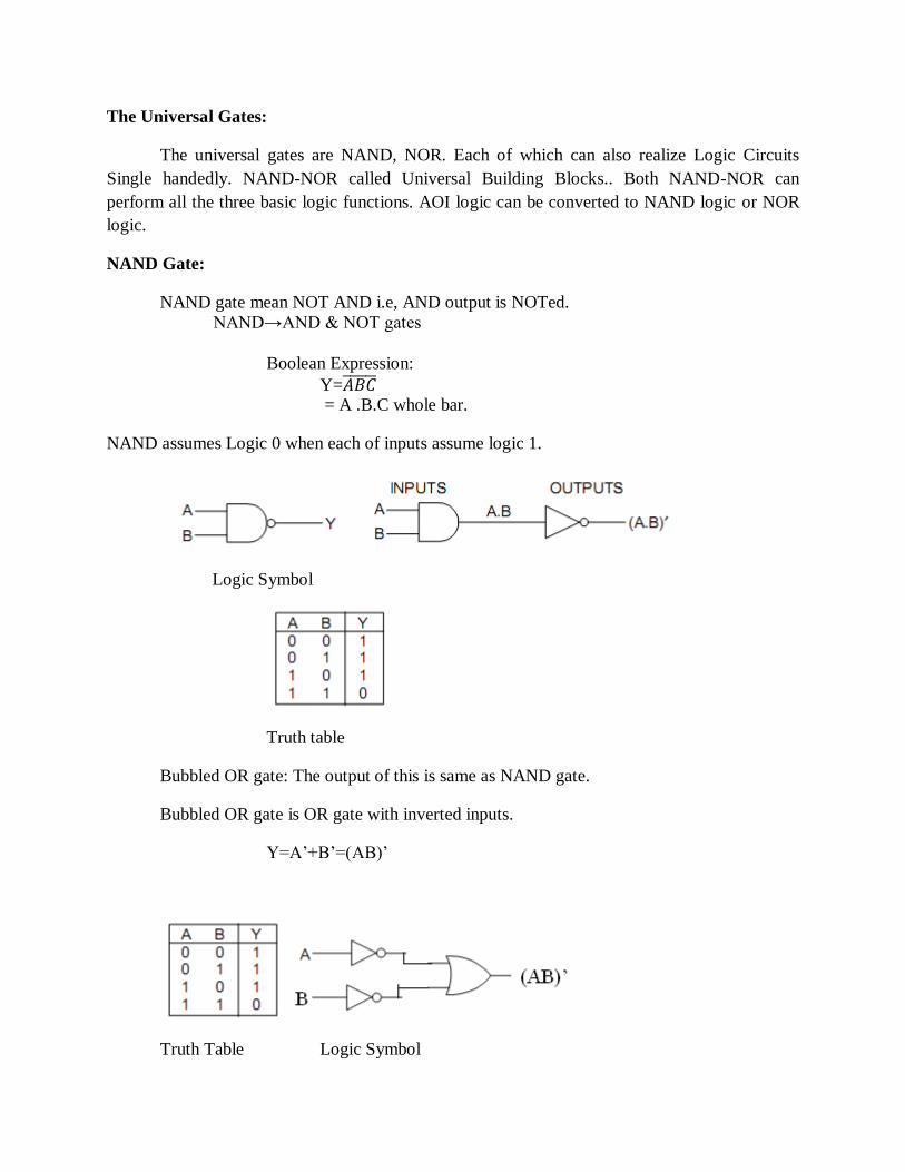
NAND Gate:
NAND gate mean NOT AND i.e, AND output is NOTed.
NAND→AND & NOT gates
Boolean Expression:
Y=𝐴𝐵𝐶 = A .B.C whole bar.
NAND assumes Logic 0 when each of inputs assume logic 1.
Logic Symbol
Truth table
Bubbled OR gate: The output of this is same as NAND gate.
Bubbled OR gate is OR gate with inverted inputs.
Y=A‘+B‘=(AB)‘
Truth Table Logic Symbol
NAND gate as an Inverter.
All its input terminals together & applying the signal to be inverted to the
common terminal by connecting all input terminals except one to logic 1 &
applying the signal to be inverted to the remaining terminal.
It is also called Controlled Inverter.
Bubbled NAND Gate:
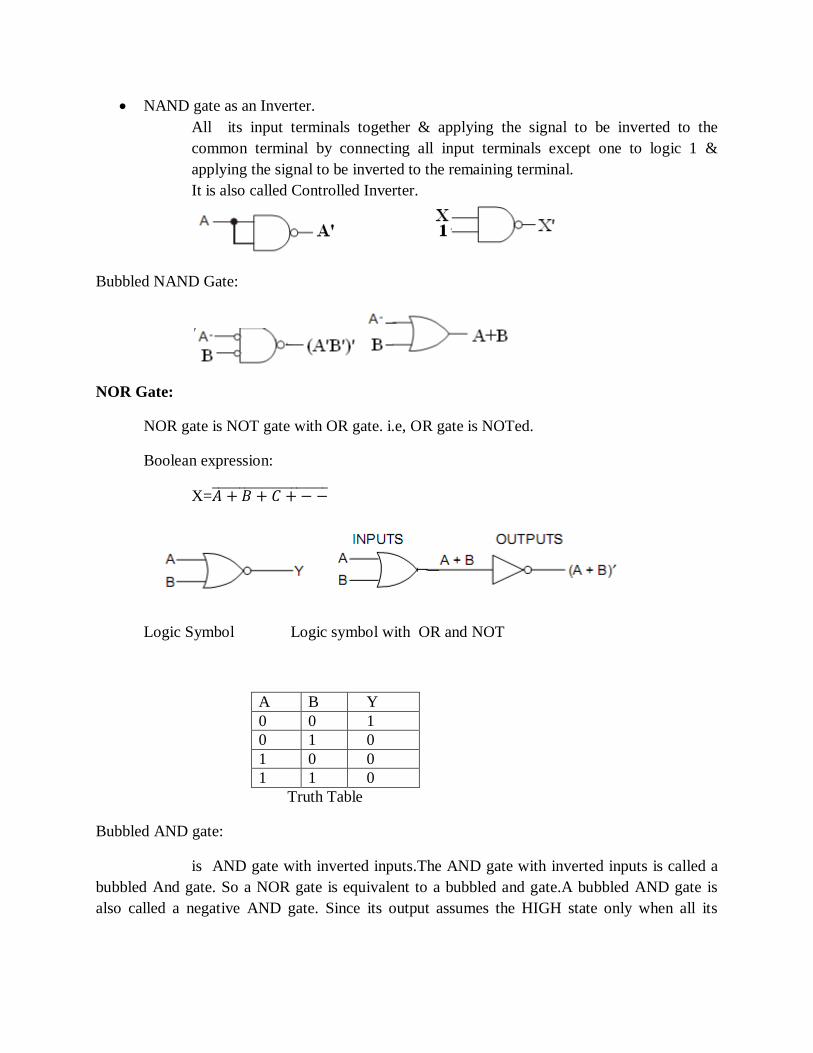
NOR Gate:
NOR gate is NOT gate with OR gate. i.e, OR gate is NOTed.
Boolean expression:
X=𝐴 + 𝐵 + 𝐶 + − −
Logic Symbol Logic symbol with OR and NOT
A B Y
0 0 1
0 1 0
1 0 0
1 1 0
Truth Table
Bubbled AND gate:
is AND gate with inverted inputs.The AND gate with inverted inputs is called a
bubbled And gate. So a NOR gate is equivalent to a bubbled and gate.A bubbled AND gate is
also called a negative AND gate. Since its output assumes the HIGH state only when all its
inputs are in LOW state , a NOR gate is also called active-LOW AND gate.Output Y is 1 only
when both A & B are equal to 0.i.e, only when both A‘ and B‘ are equal to 1.
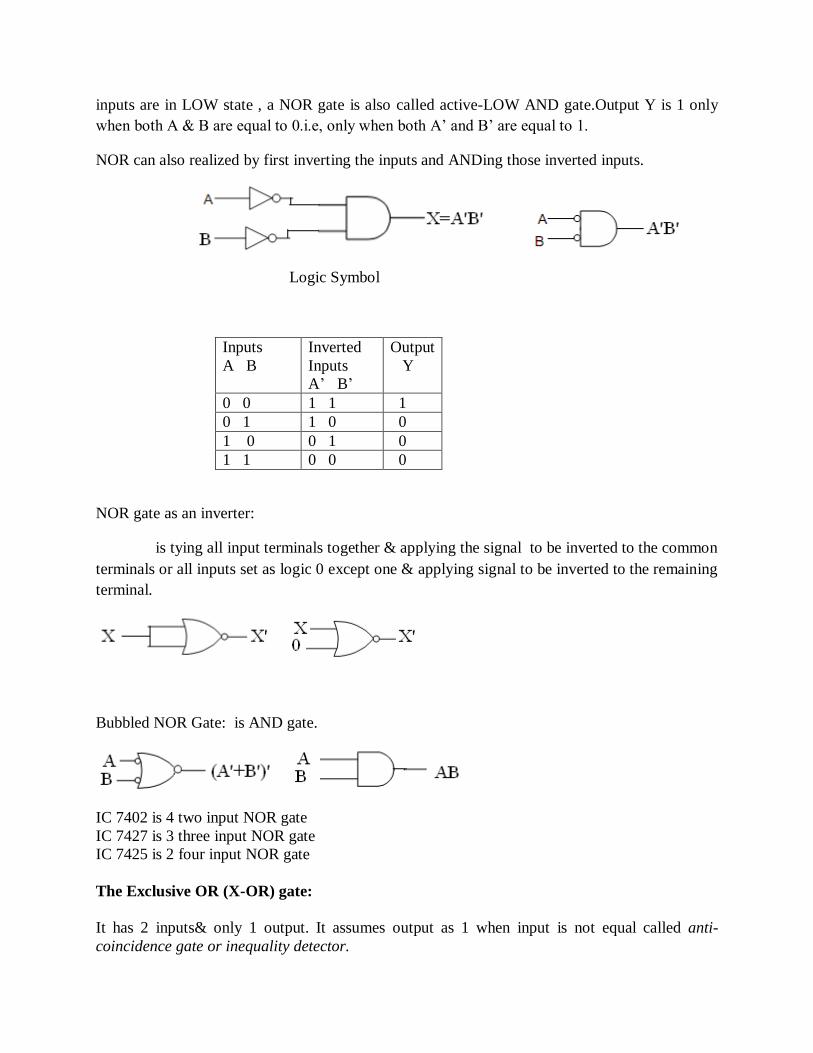
NOR can also realized by first inverting the inputs and ANDing those inverted inputs.
Logic Symbol
Inputs
A B
Inverted
Inputs
A‘ B‘
Output
Y
0 0 1 1 1
0 1 1 0 0
1 0 0 1 0
1 1 0 0 0
NOR gate as an inverter:
is tying all input terminals together & applying the signal to be inverted to the common
terminals or all inputs set as logic 0 except one & applying signal to be inverted to the remaining
terminal.
Bubbled NOR Gate: is AND gate.
IC 7402 is 4 two input NOR gate
IC 7427 is 3 three input NOR gate
IC 7425 is 2 four input NOR gate
The Exclusive OR (X-OR) gate:
It has 2 inputs& only 1 output. It assumes output as 1 when input is not equal called anti-
coincidence gate or inequality detector.
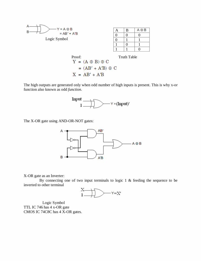
Logic Symbol
Proof: Truth Table
The high outputs are generated only when odd number of high inputs is present. This is why x-or
function also known as odd function.
The X-OR gate using AND-OR-NOT gates:
X-OR gate as an Inverter:
By connecting one of two input terminals to logic 1 & feeding the sequence to be
inverted to other terminal
Logic Symbol
TTL IC 746 has 4 x-OR gate
CMOS IC 74C8C has 4 X-OR gates.
A B 0 0 0
0 1 1
1 0 1
1 1 0
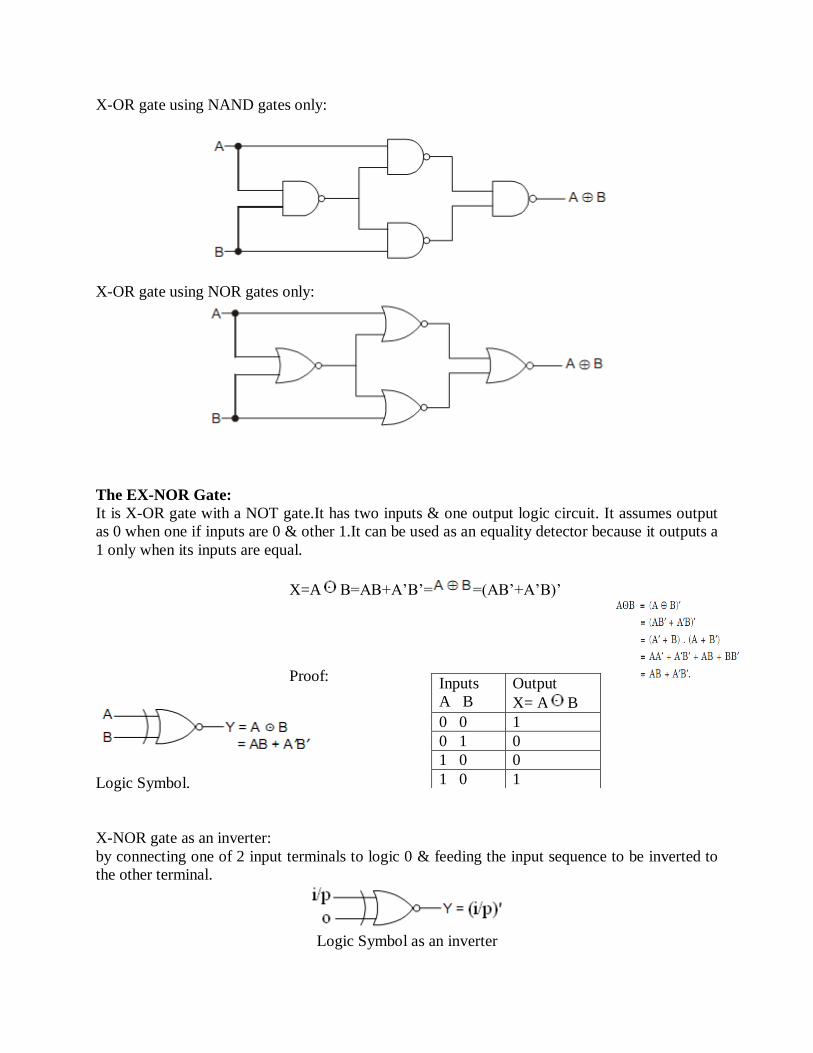
X-OR gate using NAND gates only:
X-OR gate using NOR gates only:
The EX-NOR Gate:
It is X-OR gate with a NOT gate.It has two inputs & one output logic circuit. It assumes output
as 0 when one if inputs are 0 & other 1.It can be used as an equality detector because it outputs a
1 only when its inputs are equal.
X=A B=AB+A‘B‘= =(AB‘+A‘B)‘
Proof:
Logic Symbol.
X-NOR gate as an inverter:
by connecting one of 2 input terminals to logic 0 & feeding the input sequence to be inverted to
the other terminal.
Logic Symbol as an inverter
Inputs
A B
Output
X= A B
0 0 1
0 1 0
1 0 0
1 0 1
It can be used as Controlled inverter.
A B=(A B)‘ is compliment of X-OR
A B C=(A B C)‘
TTl IC74LS266 contain 4 each X-NOR gates.
CMOS 74C266 contain 4 each X-NOR gates.
Highspeed CMOS IC 74HC266 contain 4 each X-NOR gates.
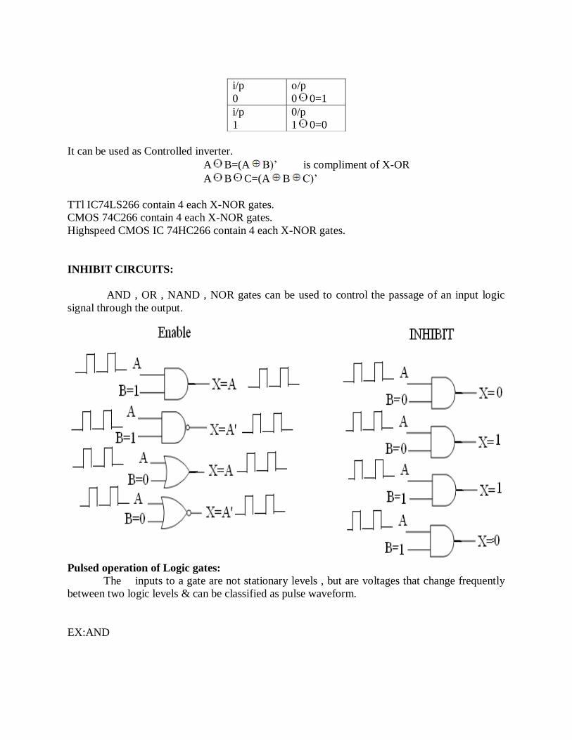
INHIBIT CIRCUITS:
AND , OR , NAND , NOR gates can be used to control the passage of an input logic
signal through the output.
Pulsed operation of Logic gates:
The inputs to a gate are not stationary levels , but are voltages that change frequently
between two logic levels & can be classified as pulse waveform.
EX:AND
i/p
0
o/p
0 0=1
i/p
1
0/p
1 0=0
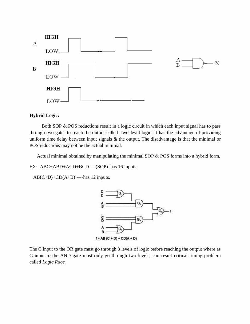
Hybrid Logic:
Both SOP & POS reductions result in a logic circuit in which each input signal has to pass
through two gates to reach the output called Two-level logic. It has the advantage of providing
uniform time delay between input signals & the output. The disadvantage is that the minimal or
POS reductions may not be the actual minimal.
Actual minimal obtained by manipulating the minimal SOP & POS forms into a hybrid form.
EX: ABC+ABD+ACD+BCD----(SOP) has 16 inputs
AB(C+D)+CD(A+B) ----has 12 inputs.
The C input to the OR gate must go through 3 levels of logic before reaching the output where as
C input to the AND gate must only go through two levels, can result critical timing problem
called Logic Race.
Implementation of Logic functions:
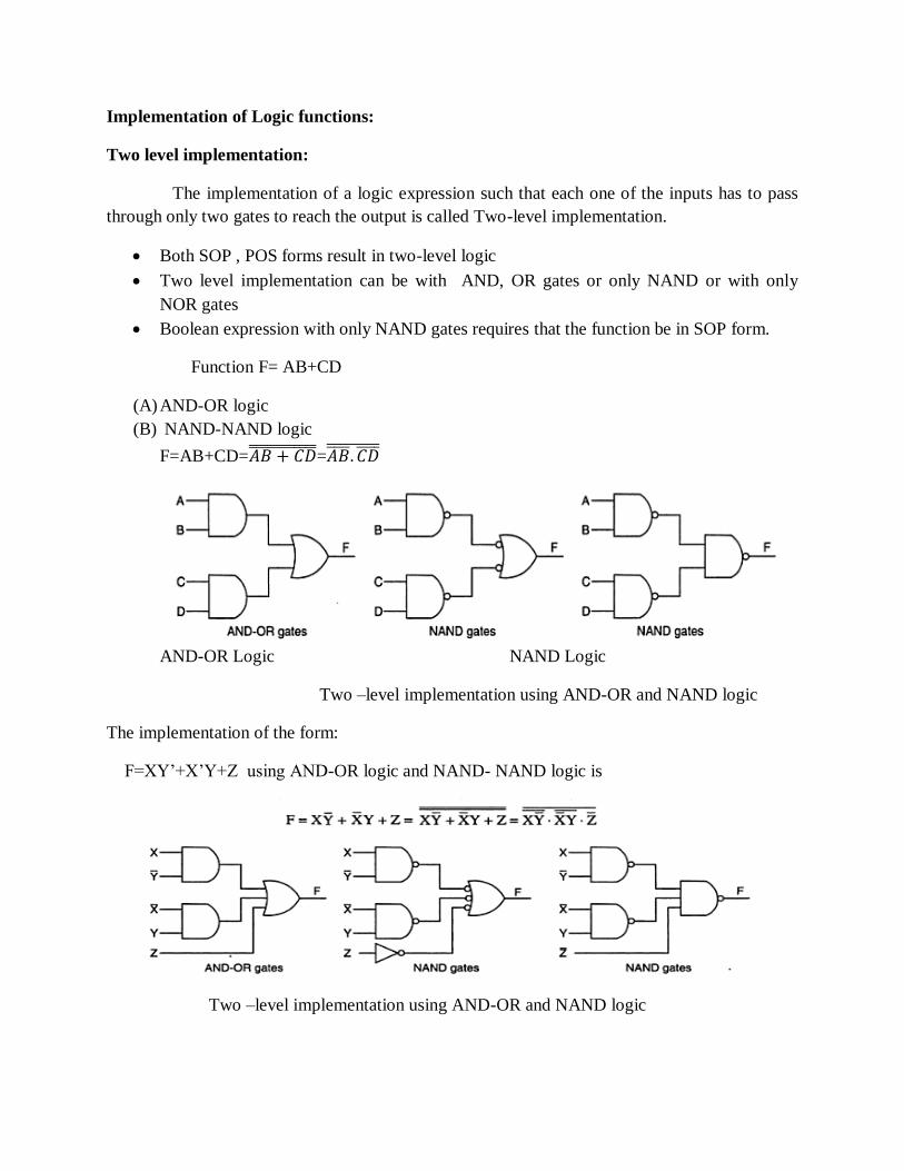
Two level implementation:
The implementation of a logic expression such that each one of the inputs has to pass
through only two gates to reach the output is called Two-level implementation.
Both SOP , POS forms result in two-level logic
Two level implementation can be with AND, OR gates or only NAND or with only
NOR gates
Boolean expression with only NAND gates requires that the function be in SOP form.
Function F= AB+CD
(A) AND-OR logic
(B) NAND-NAND logic
F=AB+CD=𝐴𝐵 + 𝐶𝐷 =𝐴𝐵 .𝐶𝐷
AND-OR Logic NAND Logic
Two –level implementation using AND-OR and NAND logic
The implementation of the form:
F=XY‘+X‘Y+Z using AND-OR logic and NAND- NAND logic is
Two –level implementation using AND-OR and NAND logic
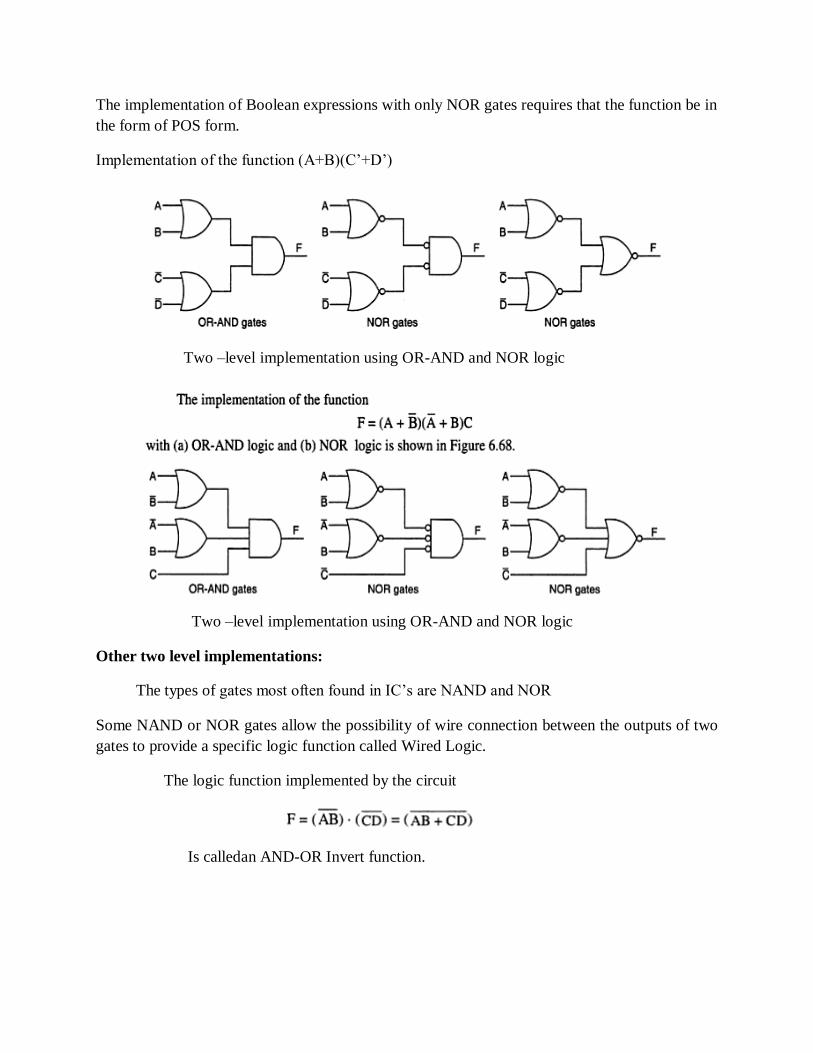
The implementation of Boolean expressions with only NOR gates requires that the function be in
the form of POS form.
Implementation of the function (A+B)(C‘+D‘)
Two –level implementation using OR-AND and NOR logic
Two –level implementation using OR-AND and NOR logic
Other two level implementations:
The types of gates most often found in IC‘s are NAND and NOR
Some NAND or NOR gates allow the possibility of wire connection between the outputs of two
gates to provide a specific logic function called Wired Logic.
The logic function implemented by the circuit
Is calledan AND-OR Invert function.
Similarly NOR outputs of ECL gates can be tied together to form Wired NOR function.
The logic function implemented by this circuit is
Is called OR-AND INVERT Function.
EX: Open Collector TTL NAND gates, when tied together perform the wired AND logic is
called AOI
=(𝐴𝐵 ) .(𝐶𝐷)
=𝐴𝐵 + 𝐶𝐷
Similarly NOR outputs of ECL can tied together to perform a wired NOR function.
F=(𝐴 + 𝐵 )+(𝐶 + 𝐷)
=[(𝐴 + 𝐵)(𝐶 + 𝐷)]
Non Degenerate forms:
Considering 4 types of gates AND, OR, NAND , NOR & assign one type of gate for
the first level & one type of gate for the second level. Find 16 possible combinations of two level
form. Eight of these are degenerate forms. Because they generate to a single operation. i.e, AND
gate in first level & AND gate in second The output is nearly the AND function of all input
variables.
The other non degenerate forms produce an implementation in SOP or POS are
AND-OR OR-AND
NAND-NAND NOR-NOR
NOR-OR NAND-NAND
OR-NAND AND-NOR
The two forms are dual of each other.
AND-OR & OR-AND forms are the basic two-level forms.
NAND-NAND, NOR_NOR
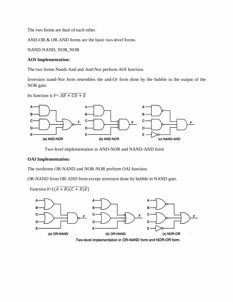
AOI Implementation:
The two forms Nandi-And and And-Nor perform AOI function.
Inversion isand-Nor form resembles the and-Or form done by the bubble in the output of the
NOR gate.
Its function is F= 𝐴𝐵 + 𝐶𝐷 + 𝐸
Two-level implementation in AND-NOR and NAND-AND form
OAI Implementation:
The twoforms OR-NAND and NOR-NOR perform OAI function.
OR-NAND form OR-AND form except inversion done by bubble in NAND gate.
Function F=[(𝐴 + 𝐵)(𝐶 + 𝐷)𝐸 ]

Summary:
Unit-II
Minimization and design of Combinational circuits
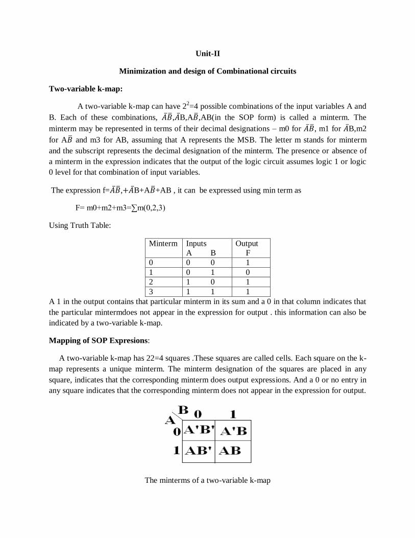
Two-variable k-map:
A two-variable k-map can have 22=4 possible combinations of the input variables A and
B. Each of these combinations, 𝐴 𝐵 ,𝐴 B,A𝐵 ,AB(in the SOP form) is called a minterm. The
minterm may be represented in terms of their decimal designations – m0 for 𝐴 𝐵 , m1 for 𝐴 B,m2
for A𝐵 and m3 for AB, assuming that A represents the MSB. The letter m stands for minterm
and the subscript represents the decimal designation of the minterm. The presence or absence of
a minterm in the expression indicates that the output of the logic circuit assumes logic 1 or logic
0 level for that combination of input variables.
The expression f=𝐴 𝐵 ,+𝐴 B+A𝐵 +AB , it can be expressed using min term as
F= m0+m2+m3=∑m(0,2,3)
Using Truth Table:
Minterm Inputs
A B
Output
F
0 0 0 1
1 0 1 0
2 1 0 1
3 1 1 1
A 1 in the output contains that particular minterm in its sum and a 0 in that column indicates that
the particular mintermdoes not appear in the expression for output . this information can also be
indicated by a two-variable k-map.
Mapping of SOP Expresions:
A two-variable k-map has 22=4 squares .These squares are called cells. Each square on the k-
map represents a unique minterm. The minterm designation of the squares are placed in any
square, indicates that the corresponding minterm does output expressions. And a 0 or no entry in
any square indicates that the corresponding minterm does not appear in the expression for output.
The minterms of a two-variable k-map
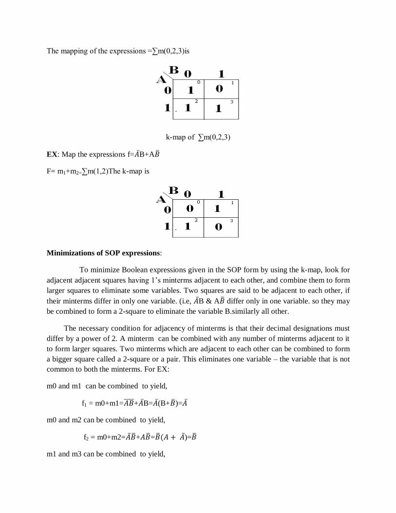
The mapping of the expressions =∑m(0,2,3)is
k-map of ∑m(0,2,3)
EX: Map the expressions f=𝐴 B+A𝐵
F= m1+m2=∑m(1,2)The k-map is
Minimizations of SOP expressions:
To minimize Boolean expressions given in the SOP form by using the k-map, look for
adjacent adjacent squares having 1‘s minterms adjacent to each other, and combine them to form
larger squares to eliminate some variables. Two squares are said to be adjacent to each other, if
their minterms differ in only one variable. (i.e, 𝐴 B & A𝐵 differ only in one variable. so they may
be combined to form a 2-square to eliminate the variable B.similarly all other.
The necessary condition for adjacency of minterms is that their decimal designations must
differ by a power of 2. A minterm can be combined with any number of minterms adjacent to it
to form larger squares. Two minterms which are adjacent to each other can be combined to form
a bigger square called a 2-square or a pair. This eliminates one variable – the variable that is not
common to both the minterms. For EX:
m0 and m1 can be combined to yield,
f1 = m0+m1=𝐴𝐵 +𝐴 B=𝐴 (B+𝐵 )=𝐴
m0 and m2 can be combined to yield,
f2 = m0+m2=𝐴 𝐵 +𝐴𝐵 =𝐵 (𝐴 + 𝐴 )=𝐵
m1 and m3 can be combined to yield,
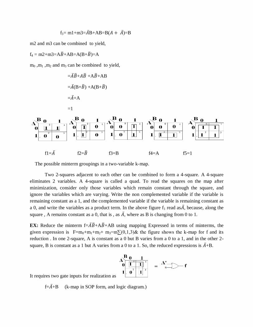
f3= m1+m3=𝐴 B+AB=B(𝐴 + 𝐴 )=B
m2 and m3 can be combined to yield,
f4 = m2+m3=A𝐵 +AB=A(B+𝐵 )=A
m0 ,m1 ,m2 and m3 can be combined to yield,
=𝐴 𝐵 +𝐴𝐵 +A𝐵 +AB
=𝐴 (B+𝐵 ) +A(B+𝐵 )
=𝐴 +A
=1
f1=𝐴 f2=𝐵 f3=B f4=A f5=1
The possible minterm groupings in a two-variable k-map.
Two 2-squares adjacent to each other can be combined to form a 4-square. A 4-square
eliminates 2 variables. A 4-square is called a quad. To read the squares on the map after
minimization, consider only those variables which remain constant through the square, and
ignore the variables which are varying. Write the non complemented variable if the variable is
remaining constant as a 1, and the complemented variable if the variable is remaining constant as
a 0, and write the variables as a product term. In the above figure f1 read as𝐴 , because, along the
square , A remains constant as a 0, that is , as 𝐴 , where as B is changing from 0 to 1.
EX: Reduce the minterm f=𝐴 𝐵 +A𝐵 +AB using mapping Expressed in terms of minterms, the
given expression is F=m0+m1+m2+ m3=m∑(0,1,3)& the figure shows the k-map for f and its
reduction . In one 2-square, A is constant as a 0 but B varies from a 0 to a 1, and in the other 2-
square, B is constant as a 1 but A varies from a 0 to a 1. So, the reduced expressions is 𝐴 +B.
It requires two gate inputs for realization as
f=𝐴 +B (k-map in SOP form, and logic diagram.)
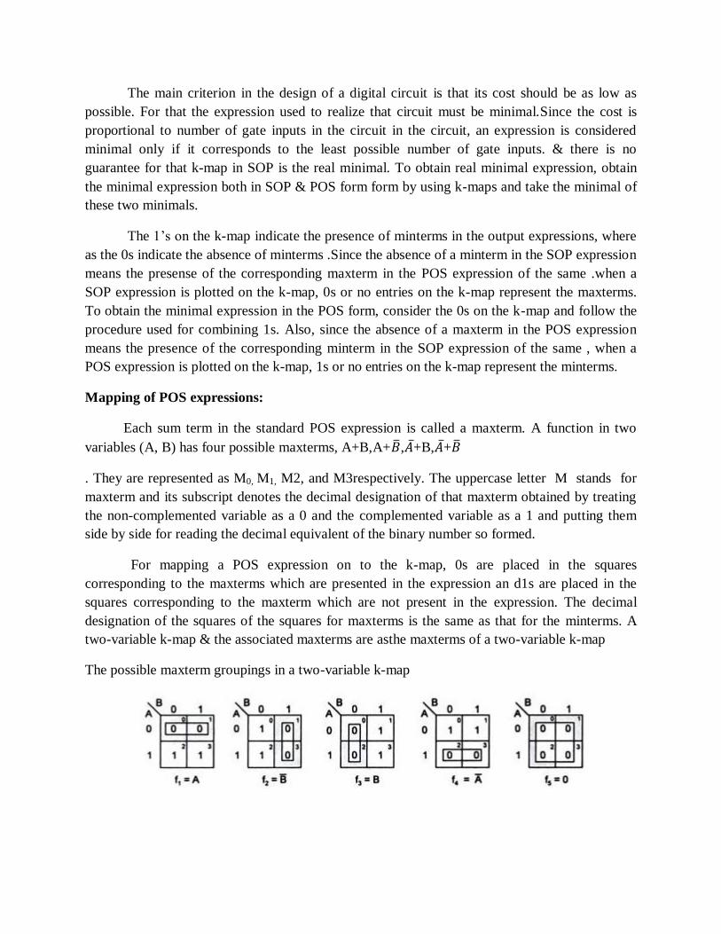
The main criterion in the design of a digital circuit is that its cost should be as low as
possible. For that the expression used to realize that circuit must be minimal.Since the cost is
proportional to number of gate inputs in the circuit in the circuit, an expression is considered
minimal only if it corresponds to the least possible number of gate inputs. & there is no
guarantee for that k-map in SOP is the real minimal. To obtain real minimal expression, obtain
the minimal expression both in SOP & POS form form by using k-maps and take the minimal of
these two minimals.
The 1‘s on the k-map indicate the presence of minterms in the output expressions, where
as the 0s indicate the absence of minterms .Since the absence of a minterm in the SOP expression
means the presense of the corresponding maxterm in the POS expression of the same .when a
SOP expression is plotted on the k-map, 0s or no entries on the k-map represent the maxterms.
To obtain the minimal expression in the POS form, consider the 0s on the k-map and follow the
procedure used for combining 1s. Also, since the absence of a maxterm in the POS expression
means the presence of the corresponding minterm in the SOP expression of the same , when a
POS expression is plotted on the k-map, 1s or no entries on the k-map represent the minterms.
Mapping of POS expressions:
Each sum term in the standard POS expression is called a maxterm. A function in two
variables (A, B) has four possible maxterms, A+B,A+𝐵 ,𝐴 +B,𝐴 +𝐵
. They are represented as M0, M1, M2, and M3respectively. The uppercase letter M stands for
maxterm and its subscript denotes the decimal designation of that maxterm obtained by treating
the non-complemented variable as a 0 and the complemented variable as a 1 and putting them
side by side for reading the decimal equivalent of the binary number so formed.
For mapping a POS expression on to the k-map, 0s are placed in the squares
corresponding to the maxterms which are presented in the expression an d1s are placed in the
squares corresponding to the maxterm which are not present in the expression. The decimal
designation of the squares of the squares for maxterms is the same as that for the minterms. A
two-variable k-map & the associated maxterms are asthe maxterms of a two-variable k-map
The possible maxterm groupings in a two-variable k-map
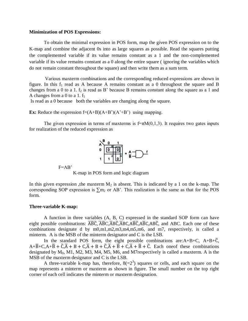
Minimization of POS Expressions:
To obtain the minimal expression in POS form, map the given POS expression on to the
K-map and combine the adjacent 0s into as large squares as possible. Read the squares putting
the complemented variable if its value remains constant as a 1 and the non-complemented
variable if its value remains constant as a 0 along the entire square ( ignoring the variables which
do not remain constant throughout the square) and then write them as a sum term.
Various maxterm combinations and the corresponding reduced expressions are shown in
figure. In this f1 read as A because A remains constant as a 0 throughout the square and B
changes from a 0 to a 1. f2 is read as B‘ because B remains constant along the square as a 1 and
A changes from a 0 to a 1. f5
Is read as a 0 because both the variables are changing along the square.
Ex: Reduce the expression f=(A+B)(A+B‘)(A‘+B‘) using mapping.
The given expression in terms of maxterms is f=πM(0,1,3). It requires two gates inputs
for realization of the reduced expression as
F=AB‘
K-map in POS form and logic diagram
In this given expression ,the maxterm M2 is absent. This is indicated by a 1 on the k-map. The
corresponding SOP expression is ∑m2 or AB‘. This realization is the same as that for the POS
form.
Three-variable K-map:
A function in three variables (A, B, C) expressed in the standard SOP form can have
eight possible combinations: A B C , A B C,A BC ,A BC,AB C ,AB C,ABC , and ABC. Each one of these
combinations designate d by m0,m1,m2,m3,m4,m5,m6, and m7, respectively, is called a
minterm. A is the MSB of the minterm designator and C is the LSB.
In the standard POS form, the eight possible combinations are:A+B+C, A+B+C ,
A+B +C,A+B + C ,A + B + C,A + B + C ,A + B + C,A + B + C . Each oneof these combinations
designated by M0, M1, M2, M3, M4, M5, M6, and M7respectively is called a maxterm. A is the
MSB of the maxterm designator and C is the LSB.
A three-variable k-map has, therefore, 8(=23) squares or cells, and each square on the
map represents a minterm or maxterm as shown in figure. The small number on the top right
corner of each cell indicates the minterm or maxterm designation.
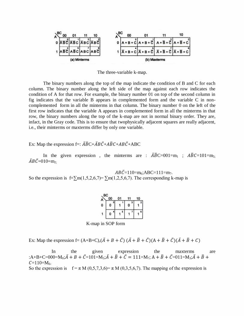
The three-variable k-map.
The binary numbers along the top of the map indicate the condition of B and C for each
column. The binary number along the left side of the map against each row indicates the
condition of A for that row. For example, the binary number 01 on top of the second column in
fig indicates that the variable B appears in complemented form and the variable C in non-
complemented form in all the minterms in that column. The binary number 0 on the left of the
first row indicates that the variable A appears in complemented form in all the minterms in that
row, the binary numbers along the top of the k-map are not in normal binary order. They are,
infact, in the Gray code. This is to ensure that twophysically adjacent squares are really adjacent,
i.e., their minterms or maxterms differ by only one variable.
Ex: Map the expression f=: 𝐴 𝐵 C+𝐴 𝐵𝐶 +𝐴𝐵 𝐶+𝐴𝐵𝐶 +ABC
In the given expression , the minterms are : 𝐴 𝐵 C=001=m1 ; 𝐴𝐵 𝐶=101=m5;
𝐴 𝐵𝐶 =010=m2;
𝐴𝐵𝐶 =110=m6;ABC=111=m7.
So the expression is f=∑m(1,5,2,6,7)= ∑m(1,2,5,6,7). The corresponding k-map is
K-map in SOP form
Ex: Map the expression f= (A+B+C),(𝐴 + 𝐵 + 𝐶 ) (𝐴 + 𝐵 + 𝐶 )(A + 𝐵 + 𝐶 )(𝐴 + 𝐵 + 𝐶)
In the given expression the maxterms are
:A+B+C=000=M0;𝐴 + 𝐵 + 𝐶 =101=M5;𝐴 + 𝐵 + 𝐶 = 111=M7; A + 𝐵 + 𝐶 =011=M3;𝐴 + 𝐵 +𝐶=110=M6.
So the expression is f = π M (0,5,7,3,6)= π M (0,3,5,6,7). The mapping of the expression is

K-map in POS form.
Minimization of SOP and POS expressions:
For reducing the Boolean expressions in SOP (POS) form plotted on the k-map, look
at the 1s (0s) present on the map. These represent the minterms (maxterms). Look for the
minterms (maxterms) adjacent to each other, in order to combine them into larger squares.
Combining of adjacent squares in a k-map containing 1s (or 0s) for the purpose of simplification
of a SOP (or POS)expression is called looping. Some of the minterms (maxterms) may have
many adjacencies. Always start with the minterms (maxterm) with the least number of
adjacencies and try to form as large as large a square as possible. The larger must form a
geometric square or rectangle. They can be formed even by wrapping around, but cannot be
formed by using diagonal configurations. Next consider the minterm (maxterm) with next to the
least number of adjacencies and form as large a square as possible. Continue this till all the
minterms (maxterms) are taken care of . A minterm (maxterm) can be part of any number of
squares if it is helpful in reduction. Read the minimal expression from the k-map, corresponding
to the squares formed. There can be more than one minimal expression.
Two squares are said to be adjacent to each other (since the binary designations along
the top of the map and those along the left side of the map are in Gray code), if they are
physically adjacent to each other, or can be made adjacent to each other by wrapping around.
For squares to be combinable into bigger squares it is essential but not sufficient that their
minterm designations must differ by a power of two.
General procedure to simplify the Boolean expressions:
1. Plot the k-map and place 1s(0s) corresponding to the minterms (maxterms) of the SOP
(POS) expression.
2. Check the k-map for 1s(0s) which are not adjacent to any other 1(0). They are isolated
minterms(maxterms) . They are to be read as they are because they cannot be combined
even into a 2-square.
3. Check for those 1s(0S) which are adjacent to only one other 1(0) and make them pairs (2
squares).
4. Check for quads (4 squares) and octets (8 squares) of adjacent 1s (0s) even if they contain
some 1s(0s) which have already been combined. They must geometrically form a square
or a rectangle.
5. Check for any 1s(0s) that have not been combined yet and combine them into bigger
squares if possible.
6. Form the minimal expression by summing (multiplying) the product the product (sum)
terms of all the groups.
Reading the K-maps:
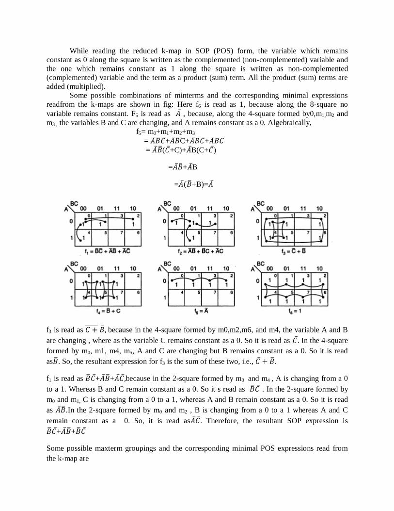
While reading the reduced k-map in SOP (POS) form, the variable which remains
constant as 0 along the square is written as the complemented (non-complemented) variable and
the one which remains constant as 1 along the square is written as non-complemented
(complemented) variable and the term as a product (sum) term. All the product (sum) terms are
added (multiplied).
Some possible combinations of minterms and the corresponding minimal expressions
readfrom the k-maps are shown in fig: Here f6 is read as 1, because along the 8-square no
variable remains constant. F5 is read as 𝐴 , because, along the 4-square formed by0,m1,m2 and
m3 , the variables B and C are changing, and A remains constant as a 0. Algebraically,
f5= m0+m1+m2+m3
= 𝐴 𝐵 𝐶 +𝐴 𝐵 C+𝐴 𝐵𝐶 +𝐴 𝐵𝐶
= 𝐴 𝐵 (𝐶 +C)+𝐴 B(C+𝐶 )
=𝐴 𝐵 +𝐴 B
=𝐴 (𝐵 +B)=𝐴
f3 is read as 𝐶 + 𝐵 , because in the 4-square formed by m0,m2,m6, and m4, the variable A and B
are changing , where as the variable C remains constant as a 0. So it is read as 𝐶 . In the 4-square
formed by m0, m1, m4, m5, A and C are changing but B remains constant as a 0. So it is read
as𝐵 . So, the resultant expression for f3 is the sum of these two, i.e., 𝐶 + 𝐵 .
f1 is read as 𝐵 𝐶 +𝐴 𝐵 +𝐴 𝐶 ,because in the 2-square formed by m0 and m4 , A is changing from a 0
to a 1. Whereas B and C remain constant as a 0. So it s read as 𝐵 𝐶 . In the 2-square formed by
m0 and m1, C is changing from a 0 to a 1, whereas A and B remain constant as a 0. So it is read
as 𝐴 𝐵 .In the 2-square formed by m0 and m2 , B is changing from a 0 to a 1 whereas A and C
remain constant as a 0. So, it is read as𝐴 𝐶 . Therefore, the resultant SOP expression is
𝐵 𝐶 +𝐴 𝐵 +𝐵 𝐶
Some possible maxterm groupings and the corresponding minimal POS expressions read from
the k-map are
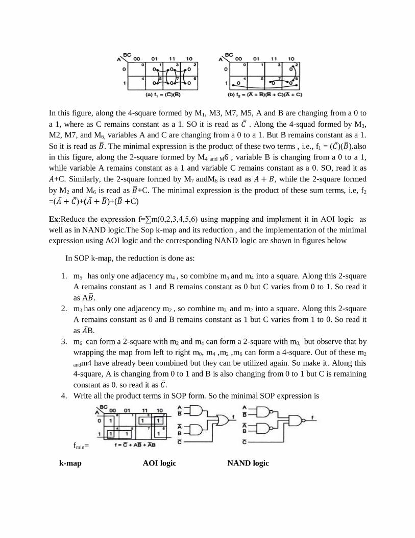
In this figure, along the 4-square formed by M1, M3, M7, M5, A and B are changing from a 0 to
a 1, where as C remains constant as a 1. SO it is read as 𝐶 . Along the 4-squad formed by M3,
M2, M7, and M6, variables A and C are changing from a 0 to a 1. But B remains constant as a 1.
So it is read as 𝐵 . The minimal expression is the product of these two terms , i.e., f1 = (𝐶 )(𝐵 ).also
in this figure, along the 2-square formed by M4 and M6 , variable B is changing from a 0 to a 1,
while variable A remains constant as a 1 and variable C remains constant as a 0. SO, read it as
𝐴 +C. Similarly, the 2-square formed by M7 andM6 is read as 𝐴 + 𝐵 , while the 2-square formed
by M2 and M6 is read as 𝐵 +C. The minimal expression is the product of these sum terms, i.e, f2
=(𝐴 + 𝐶 )+(𝐴 + 𝐵 )+(𝐵 +C)
Ex:Reduce the expression f=∑m(0,2,3,4,5,6) using mapping and implement it in AOI logic as
well as in NAND logic.The Sop k-map and its reduction , and the implementation of the minimal
expression using AOI logic and the corresponding NAND logic are shown in figures below
In SOP k-map, the reduction is done as:
1. m5 has only one adjacency m4 , so combine m5 and m4 into a square. Along this 2-square
A remains constant as 1 and B remains constant as 0 but C varies from 0 to 1. So read it
as A𝐵 .
2. m3 has only one adjacency m2 , so combine m3 and m2 into a square. Along this 2-square
A remains constant as 0 and B remains constant as 1 but C varies from 1 to 0. So read it
as 𝐴 B.
3. m6 can form a 2-square with m2 and m4 can form a 2-square with m0, but observe that by
wrapping the map from left to right m0, m4 ,m2 ,m6 can form a 4-square. Out of these m2
andm4 have already been combined but they can be utilized again. So make it. Along this
4-square, A is changing from 0 to 1 and B is also changing from 0 to 1 but C is remaining
constant as 0. so read it as 𝐶 .
4. Write all the product terms in SOP form. So the minimal SOP expression is
fmin=
k-map AOI logic NAND logic
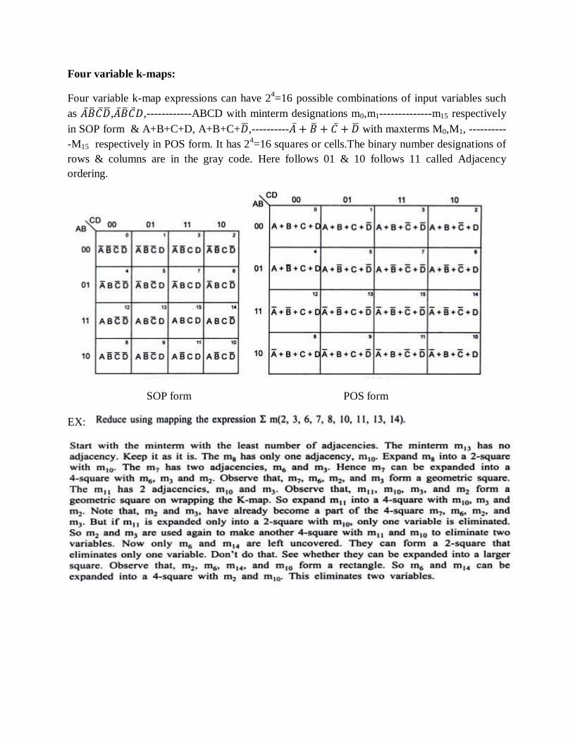
Four variable k-maps:
Four variable k-map expressions can have 24=16 possible combinations of input variables such
as 𝐴 𝐵 𝐶 𝐷 ,𝐴 𝐵 𝐶 𝐷,------------ABCD with minterm designations m0,m1--------------m15 respectively
in SOP form & A+B+C+D, A+B+C+𝐷 ,----------𝐴 + 𝐵 + 𝐶 + 𝐷 with maxterms M0,M1, ----------
-M15 respectively in POS form. It has 24=16 squares or cells.The binary number designations of
rows & columns are in the gray code. Here follows 01 & 10 follows 11 called Adjacency
ordering.
SOP form POS form
EX:
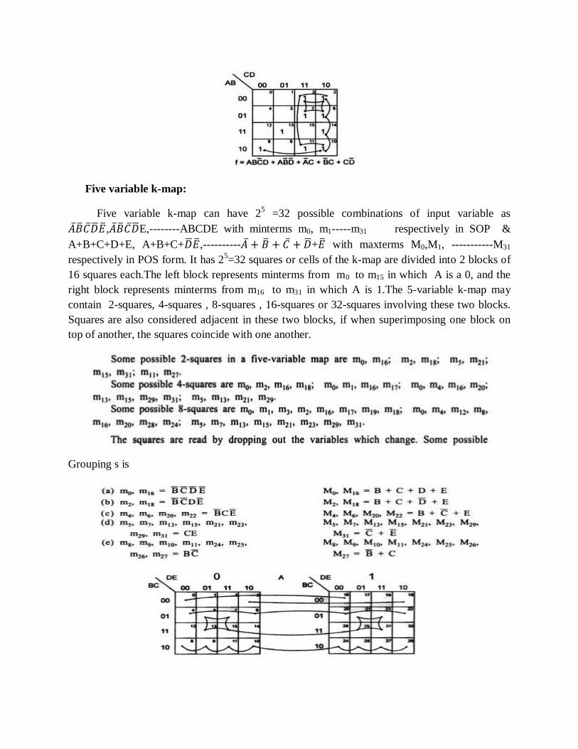
Five variable k-map:
Five variable k-map can have 25 =32 possible combinations of input variable as
𝐴 𝐵 𝐶 𝐷 𝐸 ,𝐴 𝐵 𝐶 𝐷 E,--------ABCDE with minterms m0, m1-----m31 respectively in SOP &
A+B+C+D+E, A+B+C+𝐷 𝐸 ,----------𝐴 + 𝐵 + 𝐶 + 𝐷 +𝐸 with maxterms M0,M1, -----------M31
respectively in POS form. It has 25=32 squares or cells of the k-map are divided into 2 blocks of
16 squares each.The left block represents minterms from m0 to m15 in which A is a 0, and the
right block represents minterms from m16 to m31 in which A is 1.The 5-variable k-map may
contain 2-squares, 4-squares , 8-squares , 16-squares or 32-squares involving these two blocks.
Squares are also considered adjacent in these two blocks, if when superimposing one block on
top of another, the squares coincide with one another.
Grouping s is
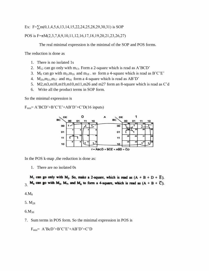
Ex: F=∑m(0,1,4,5,6,13,14,15,22,24,25,28,29,30,31) is SOP
POS is F=πM(2,3,7,8,9,10,11,12,16,17,18,19,20,21,23,26,27)
The real minimal expression is the minimal of the SOP and POS forms.
The reduction is done as
1. There is no isolated 1s
2. M12 can go only with m13. Form a 2-square which is read as A‘BCD‘
3. M0 can go with m2,m16 and m18 . so form a 4-square which is read as B‘C‘E‘
4. M20,m21,m17 and m16 form a 4-square which is read as AB‘D‘
5. M2,m3,m18,m19,m10,m11,m26 and m27 form an 8-square which is read as C‘d
6. Write all the product terms in SOP form.
So the minimal expression is
Fmin= A‘BCD‘+B‘C‘E‘+AB‘D‘+C‘D(16 inputs)
In the POS k-map ,the reduction is done as:
1. There are no isolated 0s
3.
4.M8
5. M28
6.M30
7. Sum terms in POS form. So the minimal expression in POS is
Fmin= A‘BcD‘+B‘C‘E‘+AB‘D‘+C‘D
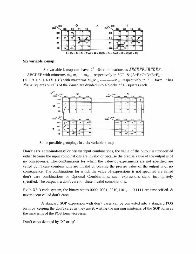
Six variable k-map:
Six variable k-map can have 26
=64 combinations as 𝐴 𝐵 𝐶 𝐷 𝐸 𝐹 ,𝐴 𝐵 𝐶 𝐷 𝐸 𝐹,---------
---ABCDEF with minterms m0, m1-----m63 respectively in SOP & (A+B+C+D+E+F),----------
(𝐴 + 𝐵 + 𝐶 + 𝐷 +𝐸 + 𝐹 ) with maxterms M0,M1, -----------M63 respectively in POS form. It has
26=64 squares or cells of the k-map are divided into 4 blocks of 16 squares each.
Some possible groupings in a six variable k-map
Don’t care combinations:For certain input combinations, the value of the output is unspecified
either because the input combinations are invalid or because the precise value of the output is of
no consequence. The combinations for which the value of experiments are not specified are
called don‘t care combinations are invalid or because the precise value of the output is of no
consequence. The combinations for which the value of expressions is not specified are called
don‘t care combinations or Optional Combinations, such expressions stand incompletely
specified. The output is a don‘t care for these invalid combinations.
Ex:In XS-3 code system, the binary states 0000, 0001, 0010,1101,1110,1111 are unspecified. &
never occur called don‘t cares.
A standard SOP expression with don‘t cares can be converted into a standard POS
form by keeping the don‘t cares as they are & writing the missing minterms of the SOP form as
the maxterms of the POS form viceversa.
Don‘t cares denoted by ‗X‘ or ‗φ‘
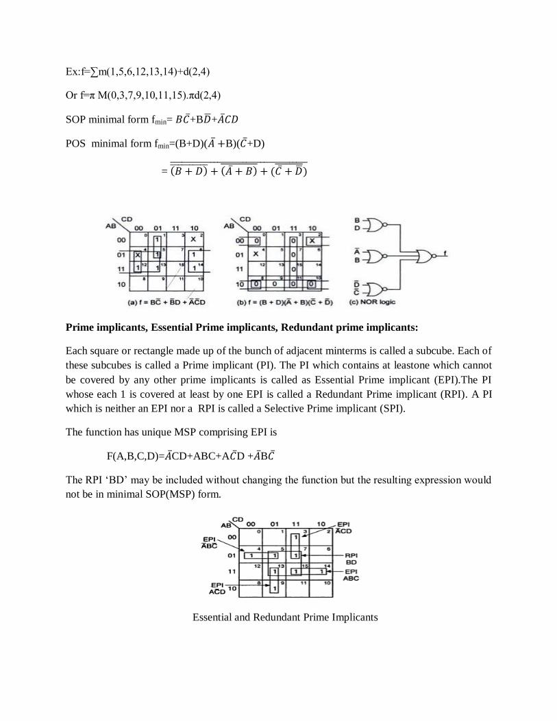
Ex:f=∑m(1,5,6,12,13,14)+d(2,4)
Or f=π M(0,3,7,9,10,11,15).πd(2,4)
SOP minimal form fmin= 𝐵𝐶 +B𝐷 +𝐴 𝐶𝐷
POS minimal form fmin=(B+D)(𝐴 +B)(𝐶 +D)
= 𝐵 + 𝐷 + 𝐴 + 𝐵 + (𝐶 + 𝐷 )
Prime implicants, Essential Prime implicants, Redundant prime implicants:
Each square or rectangle made up of the bunch of adjacent minterms is called a subcube. Each of
these subcubes is called a Prime implicant (PI). The PI which contains at leastone which cannot
be covered by any other prime implicants is called as Essential Prime implicant (EPI).The PI
whose each 1 is covered at least by one EPI is called a Redundant Prime implicant (RPI). A PI
which is neither an EPI nor a RPI is called a Selective Prime implicant (SPI).
The function has unique MSP comprising EPI is
F(A,B,C,D)=𝐴 CD+ABC+A𝐶 D +𝐴 B𝐶
The RPI ‗BD‘ may be included without changing the function but the resulting expression would
not be in minimal SOP(MSP) form.
Essential and Redundant Prime Implicants
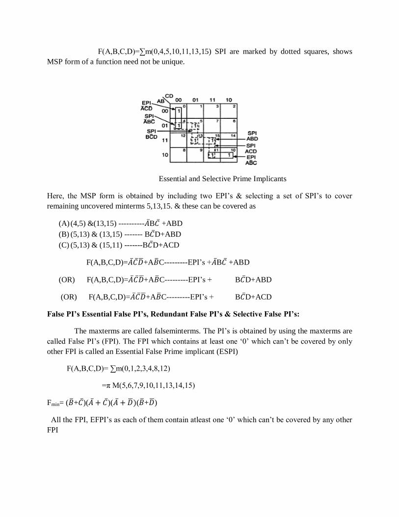
F(A,B,C,D)=∑m(0,4,5,10,11,13,15) SPI are marked by dotted squares, shows
MSP form of a function need not be unique.
Essential and Selective Prime Implicants
Here, the MSP form is obtained by including two EPI‘s & selecting a set of SPI‘s to cover
remaining uncovered minterms 5,13,15. & these can be covered as
(A) (4,5) &(13,15) ----------𝐴 B𝐶 +ABD
(B) (5,13) & (13,15) ------- B𝐶 D+ABD
(C) (5,13) & (15,11) -------B𝐶 D+ACD
F(A,B,C,D)=𝐴 𝐶 𝐷 +A𝐵 C---------EPI‘s + 𝐴 B𝐶 +ABD
(OR) F(A,B,C,D)=𝐴 𝐶 𝐷 +A𝐵 C---------EPI‘s + B𝐶 D+ABD
(OR) F(A,B,C,D)=𝐴 𝐶 𝐷 +A𝐵 C---------EPI‘s + B𝐶 D+ACD
False PI’s Essential False PI’s, Redundant False PI’s & Selective False PI’s:
The maxterms are called falseminterms. The PI‘s is obtained by using the maxterms are
called False PI‘s (FPI). The FPI which contains at least one ‗0‘ which can‘t be covered by only
other FPI is called an Essential False Prime implicant (ESPI)
F(A,B,C,D)= ∑m(0,1,2,3,4,8,12)
=π M(5,6,7,9,10,11,13,14,15)
Fmin= (𝐵 +𝐶 )(𝐴 + 𝐶 )(𝐴 + 𝐷 )(𝐵 +𝐷 )
All the FPI, EFPI‘s as each of them contain atleast one ‗0‘ which can‘t be covered by any other
FPI
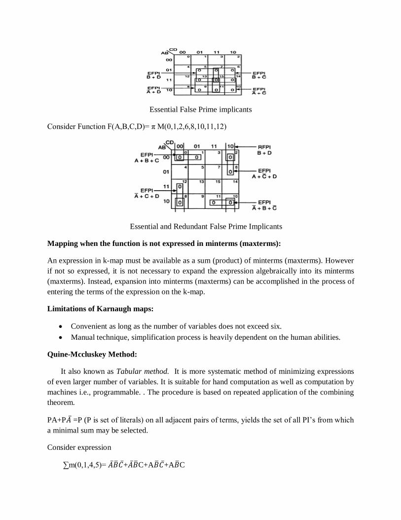
Essential False Prime implicants
Consider Function F(A,B,C,D)= π M(0,1,2,6,8,10,11,12)
Essential and Redundant False Prime Implicants
Mapping when the function is not expressed in minterms (maxterms):
An expression in k-map must be available as a sum (product) of minterms (maxterms). However
if not so expressed, it is not necessary to expand the expression algebraically into its minterms
(maxterms). Instead, expansion into minterms (maxterms) can be accomplished in the process of
entering the terms of the expression on the k-map.
Limitations of Karnaugh maps:
Convenient as long as the number of variables does not exceed six.
Manual technique, simplification process is heavily dependent on the human abilities.
Quine-Mccluskey Method:
It also known as Tabular method. It is more systematic method of minimizing expressions
of even larger number of variables. It is suitable for hand computation as well as computation by
machines i.e., programmable. . The procedure is based on repeated application of the combining
theorem.
PA+P𝐴 =P (P is set of literals) on all adjacent pairs of terms, yields the set of all PI‘s from which
a minimal sum may be selected.
Consider expression
∑m(0,1,4,5)= 𝐴 𝐵 𝐶 +𝐴 𝐵 C+A𝐵 𝐶 +A𝐵 C
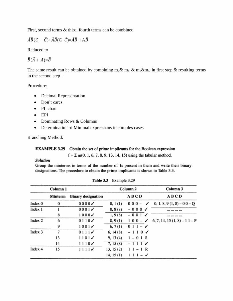
First, second terms & third, fourth terms can be combined
𝐴 𝐵 (𝐶 + 𝐶 )+𝐴 𝐵 (C+𝐶 )=𝐴 𝐵 +A𝐵
Reduced to
𝐵 (𝐴 + 𝐴)=𝐵
The same result can be obtained by combining m0& m4 & m1&m5 in first step & resulting terms
in the second step .
Procedure:
Decimal Representation
Don‘t cares
PI chart
EPI
Dominating Rows & Columns
Determination of Minimal expressions in comples cases.
Branching Method:

EX:
Combinational Logic Design
Logic circuits for digital systems may be combinational or sequential. The output of a
combinational circuit depends on its present inputs only .Combinational circuit processing
operation fully specified logically by a set of Boolean functions .A combinational circuit consists
of input variables, logic gates and output variables.Both input and output data are represented by
signals, i.e., they exists in two possible values. One is logic –1 and the other logic 0.
For n input variables,there are 2n possible combinations of binary input variables .For
each possible input Combination ,there is one and only one possible output combination.A
combinational circuit can be described by m Boolean functions one for each output
variables.Usually the input s comes from flip-flops and outputs goto flip-flops.
Design Procedure:
1.The problem is stated
2. The number of available input variables and required output variables is determined.
3.The input and output variables are assigned letter symbols.
4.The truth table that defines the required relationship between inputs and outputs is derived.
5.The simplified Boolean function for each output is obtained.
6.The logic diagram is drawn.
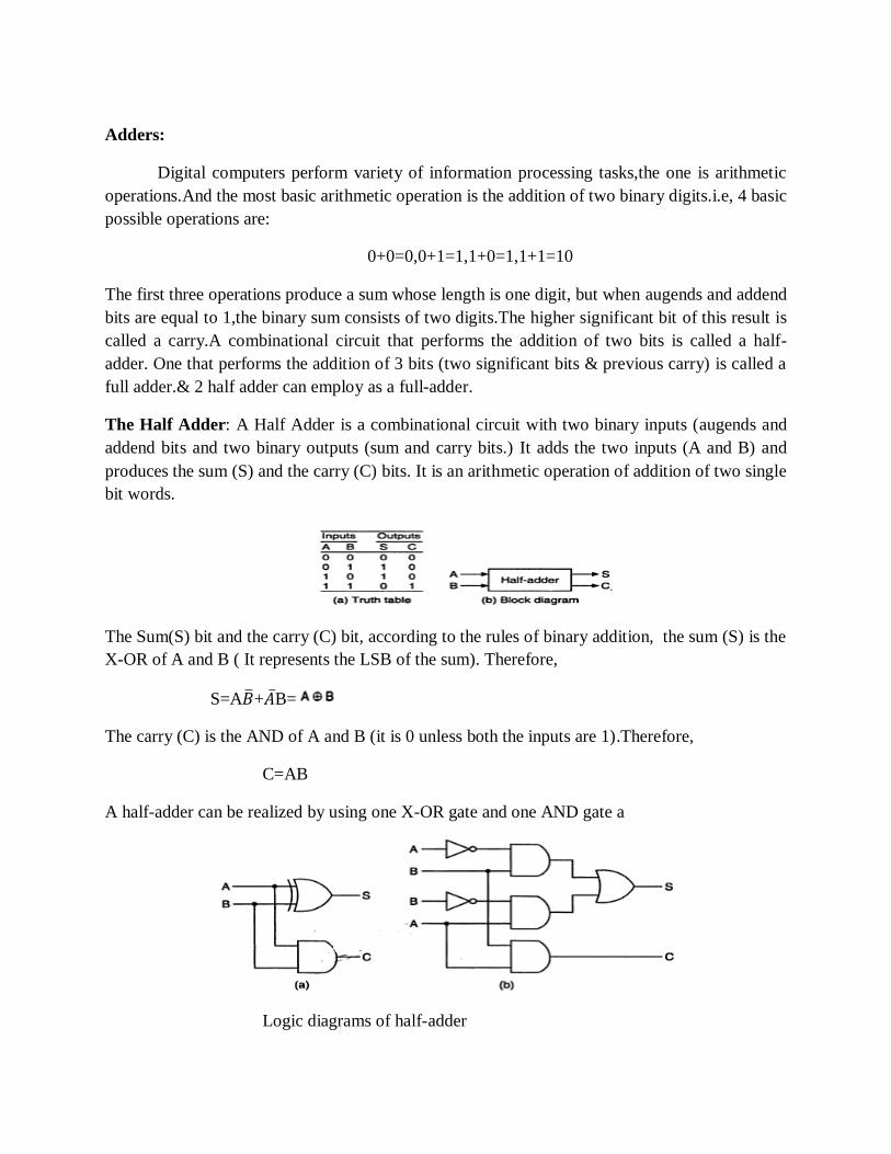
Adders:
Digital computers perform variety of information processing tasks,the one is arithmetic
operations.And the most basic arithmetic operation is the addition of two binary digits.i.e, 4 basic
possible operations are:
0+0=0,0+1=1,1+0=1,1+1=10
The first three operations produce a sum whose length is one digit, but when augends and addend
bits are equal to 1,the binary sum consists of two digits.The higher significant bit of this result is
called a carry.A combinational circuit that performs the addition of two bits is called a half-
adder. One that performs the addition of 3 bits (two significant bits & previous carry) is called a
full adder.& 2 half adder can employ as a full-adder.
The Half Adder: A Half Adder is a combinational circuit with two binary inputs (augends and
addend bits and two binary outputs (sum and carry bits.) It adds the two inputs (A and B) and
produces the sum (S) and the carry (C) bits. It is an arithmetic operation of addition of two single
bit words.
The Sum(S) bit and the carry (C) bit, according to the rules of binary addition, the sum (S) is the
X-OR of A and B ( It represents the LSB of the sum). Therefore,
S=A𝐵 +𝐴 B=
The carry (C) is the AND of A and B (it is 0 unless both the inputs are 1).Therefore,
C=AB
A half-adder can be realized by using one X-OR gate and one AND gate a
Logic diagrams of half-adder
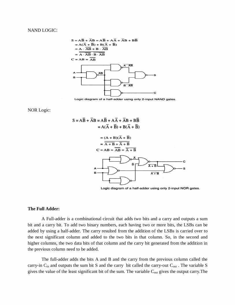
NAND LOGIC:
NOR Logic:
The Full Adder:
A Full-adder is a combinational circuit that adds two bits and a carry and outputs a sum
bit and a carry bit. To add two binary numbers, each having two or more bits, the LSBs can be
added by using a half-adder. The carry resulted from the addition of the LSBs is carried over to
the next significant column and added to the two bits in that column. So, in the second and
higher columns, the two data bits of that column and the carry bit generated from the addition in
the previous column need to be added.
The full-adder adds the bits A and B and the carry from the previous column called the
carry-in Cin and outputs the sum bit S and the carry bit called the carry-out Cout . The variable S
gives the value of the least significant bit of the sum. The variable Cout gives the output carry.The
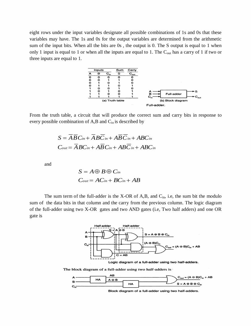
eight rows under the input variables designate all possible combinations of 1s and 0s that these
variables may have. The 1s and 0s for the output variables are determined from the arithmetic
sum of the input bits. When all the bits are 0s , the output is 0. The S output is equal to 1 when
only 1 input is equal to 1 or when all the inputs are equal to 1. The Cout has a carry of 1 if two or
three inputs are equal to 1.
From the truth table, a circuit that will produce the correct sum and carry bits in response to
every possible combination of A,B and Cin is described by
and
The sum term of the full-adder is the X-OR of A,B, and Cin, i.e, the sum bit the modulo
sum of the data bits in that column and the carry from the previous column. The logic diagram
of the full-adder using two X-OR gates and two AND gates (i.e, Two half adders) and one OR
gate is
ABBCACC
CBAS
ininout
in
ininininout
inininin
ABCCABCBABCAC
ABCCBACBACBAS
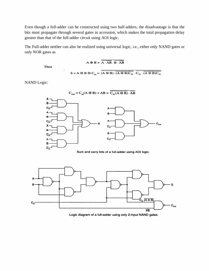
Even though a full-adder can be constructed using two half-adders, the disadvantage is that the
bits must propagate through several gates in accession, which makes the total propagation delay
greater than that of the full-adder circuit using AOI logic.
The Full-adder neither can also be realized using universal logic, i.e., either only NAND gates or
only NOR gates as
NAND Logic:
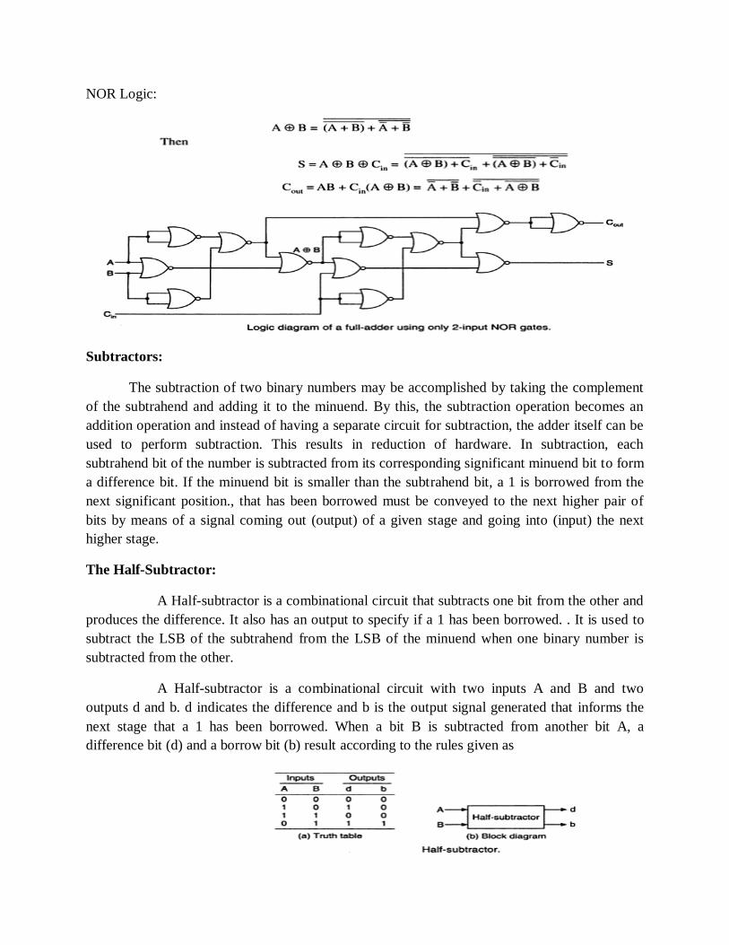
NOR Logic:
Subtractors:
The subtraction of two binary numbers may be accomplished by taking the complement
of the subtrahend and adding it to the minuend. By this, the subtraction operation becomes an
addition operation and instead of having a separate circuit for subtraction, the adder itself can be
used to perform subtraction. This results in reduction of hardware. In subtraction, each
subtrahend bit of the number is subtracted from its corresponding significant minuend bit to form
a difference bit. If the minuend bit is smaller than the subtrahend bit, a 1 is borrowed from the
next significant position., that has been borrowed must be conveyed to the next higher pair of
bits by means of a signal coming out (output) of a given stage and going into (input) the next
higher stage.
The Half-Subtractor:
A Half-subtractor is a combinational circuit that subtracts one bit from the other and
produces the difference. It also has an output to specify if a 1 has been borrowed. . It is used to
subtract the LSB of the subtrahend from the LSB of the minuend when one binary number is
subtracted from the other.
A Half-subtractor is a combinational circuit with two inputs A and B and two
outputs d and b. d indicates the difference and b is the output signal generated that informs the
next stage that a 1 has been borrowed. When a bit B is subtracted from another bit A, a
difference bit (d) and a borrow bit (b) result according to the rules given as
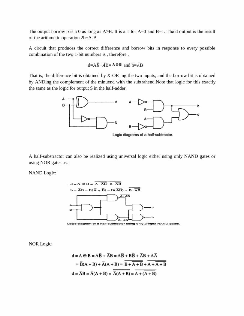
The output borrow b is a 0 as long as A≥B. It is a 1 for A=0 and B=1. The d output is the result
of the arithmetic operation 2b+A-B.
A circuit that produces the correct difference and borrow bits in response to every possible
combination of the two 1-bit numbers is , therefore ,
d=A𝐵 +𝐴 B= and b=𝐴 B
That is, the difference bit is obtained by X-OR ing the two inputs, and the borrow bit is obtained
by ANDing the complement of the minuend with the subtrahend.Note that logic for this exactly
the same as the logic for output S in the half-adder.
A half-substractor can also be realized using universal logic either using only NAND gates or
using NOR gates as:
NAND Logic:
NOR Logic:
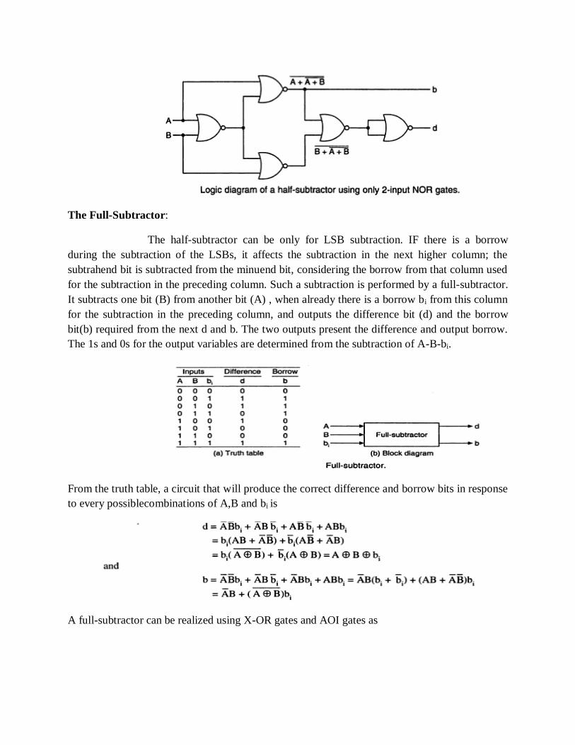
The Full-Subtractor:
The half-subtractor can be only for LSB subtraction. IF there is a borrow
during the subtraction of the LSBs, it affects the subtraction in the next higher column; the
subtrahend bit is subtracted from the minuend bit, considering the borrow from that column used
for the subtraction in the preceding column. Such a subtraction is performed by a full-subtractor.
It subtracts one bit (B) from another bit (A) , when already there is a borrow bi from this column
for the subtraction in the preceding column, and outputs the difference bit (d) and the borrow
bit(b) required from the next d and b. The two outputs present the difference and output borrow.
The 1s and 0s for the output variables are determined from the subtraction of A-B-bi.
From the truth table, a circuit that will produce the correct difference and borrow bits in response
to every possiblecombinations of A,B and bi is
A full-subtractor can be realized using X-OR gates and AOI gates as
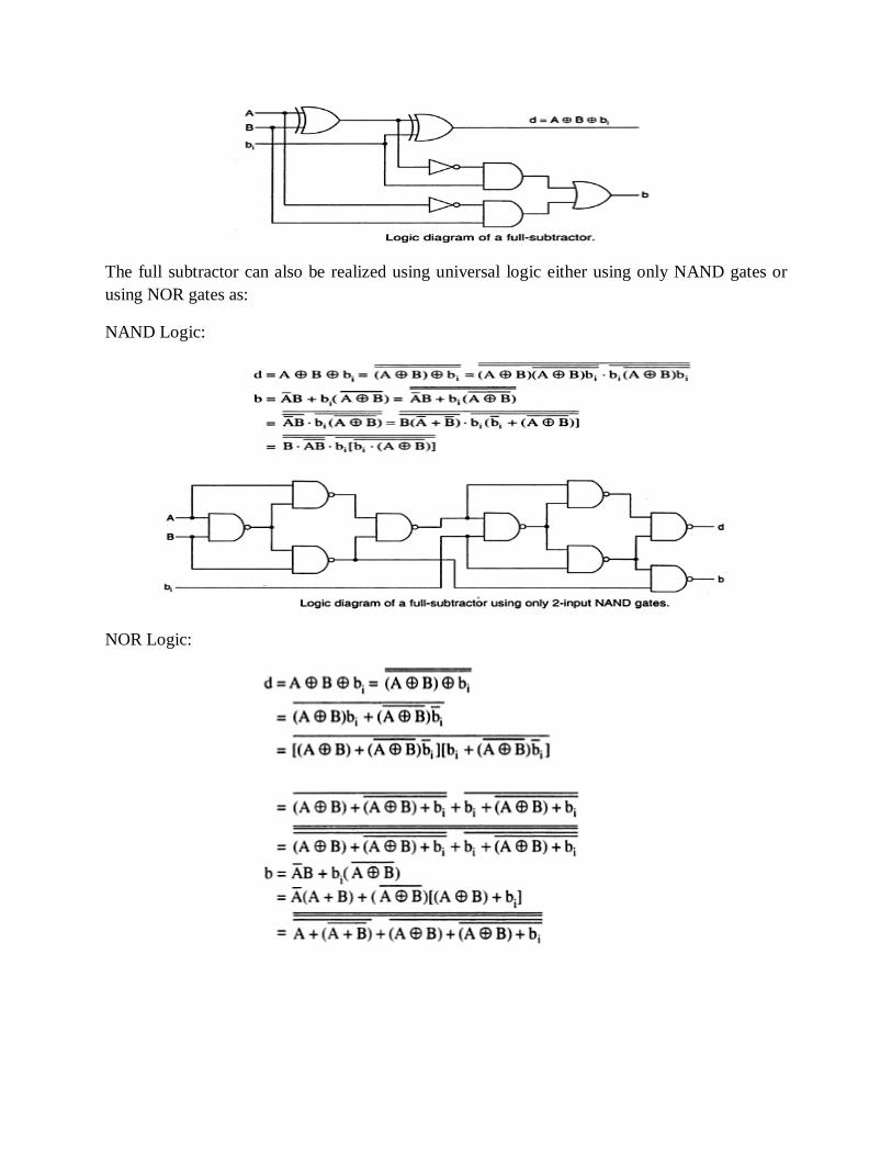
The full subtractor can also be realized using universal logic either using only NAND gates or
using NOR gates as:
NAND Logic:
NOR Logic:
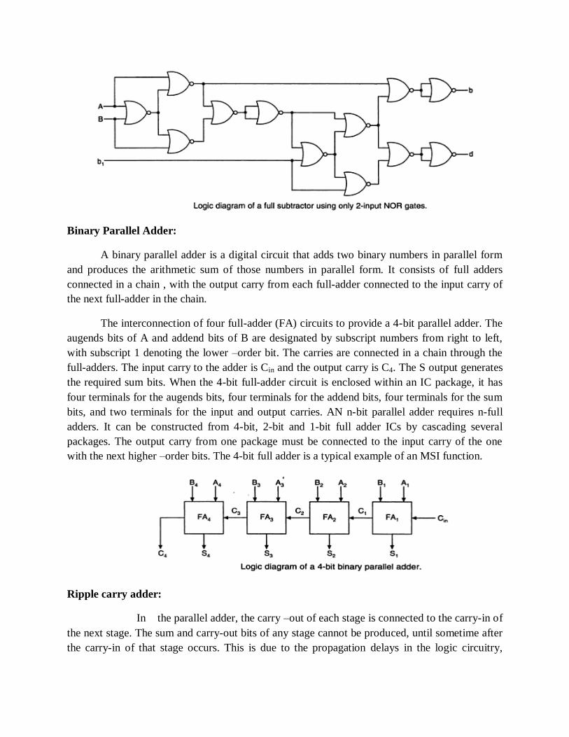
Binary Parallel Adder:
A binary parallel adder is a digital circuit that adds two binary numbers in parallel form
and produces the arithmetic sum of those numbers in parallel form. It consists of full adders
connected in a chain , with the output carry from each full-adder connected to the input carry of
the next full-adder in the chain.
The interconnection of four full-adder (FA) circuits to provide a 4-bit parallel adder. The
augends bits of A and addend bits of B are designated by subscript numbers from right to left,
with subscript 1 denoting the lower –order bit. The carries are connected in a chain through the
full-adders. The input carry to the adder is Cin and the output carry is C4. The S output generates
the required sum bits. When the 4-bit full-adder circuit is enclosed within an IC package, it has
four terminals for the augends bits, four terminals for the addend bits, four terminals for the sum
bits, and two terminals for the input and output carries. AN n-bit parallel adder requires n-full
adders. It can be constructed from 4-bit, 2-bit and 1-bit full adder ICs by cascading several
packages. The output carry from one package must be connected to the input carry of the one
with the next higher –order bits. The 4-bit full adder is a typical example of an MSI function.
Ripple carry adder:
In the parallel adder, the carry –out of each stage is connected to the carry-in of
the next stage. The sum and carry-out bits of any stage cannot be produced, until sometime after
the carry-in of that stage occurs. This is due to the propagation delays in the logic circuitry,
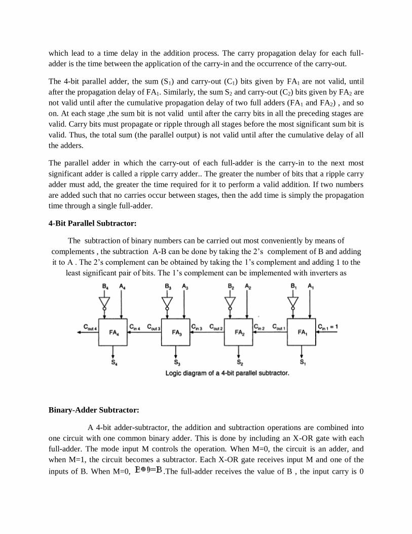
which lead to a time delay in the addition process. The carry propagation delay for each full-
adder is the time between the application of the carry-in and the occurrence of the carry-out.
The 4-bit parallel adder, the sum (S1) and carry-out (C1) bits given by FA1 are not valid, until
after the propagation delay of FA1. Similarly, the sum S2 and carry-out (C2) bits given by FA2 are
not valid until after the cumulative propagation delay of two full adders (FA1 and FA2) , and so
on. At each stage ,the sum bit is not valid until after the carry bits in all the preceding stages are
valid. Carry bits must propagate or ripple through all stages before the most significant sum bit is
valid. Thus, the total sum (the parallel output) is not valid until after the cumulative delay of all
the adders.
The parallel adder in which the carry-out of each full-adder is the carry-in to the next most
significant adder is called a ripple carry adder.. The greater the number of bits that a ripple carry
adder must add, the greater the time required for it to perform a valid addition. If two numbers
are added such that no carries occur between stages, then the add time is simply the propagation
time through a single full-adder.
4-Bit Parallel Subtractor:
The subtraction of binary numbers can be carried out most conveniently by means of
complements , the subtraction A-B can be done by taking the 2‘s complement of B and adding
it to A . The 2‘s complement can be obtained by taking the 1‘s complement and adding 1 to the
least significant pair of bits. The 1‘s complement can be implemented with inverters as
Binary-Adder Subtractor:
A 4-bit adder-subtractor, the addition and subtraction operations are combined into
one circuit with one common binary adder. This is done by including an X-OR gate with each
full-adder. The mode input M controls the operation. When M=0, the circuit is an adder, and
when M=1, the circuit becomes a subtractor. Each X-OR gate receives input M and one of the
inputs of B. When M=0, .The full-adder receives the value of B , the input carry is 0
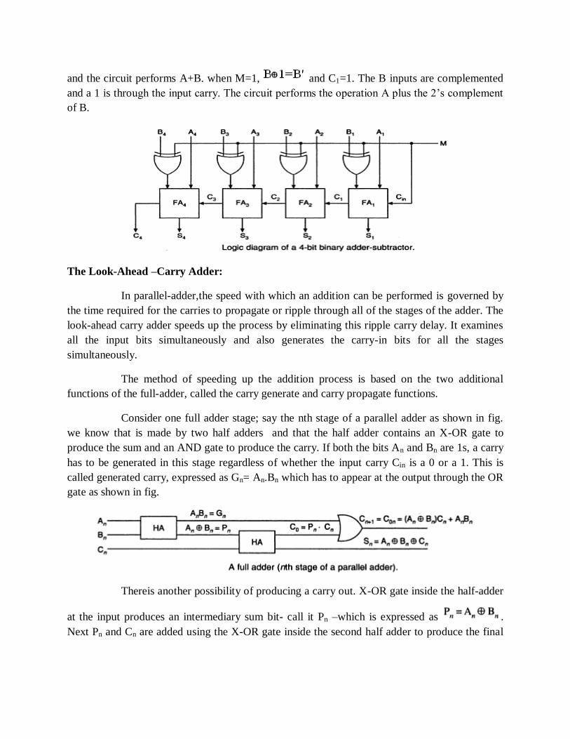
and the circuit performs A+B. when M=1, and C1=1. The B inputs are complemented
and a 1 is through the input carry. The circuit performs the operation A plus the 2‘s complement
of B.
The Look-Ahead –Carry Adder:
In parallel-adder,the speed with which an addition can be performed is governed by
the time required for the carries to propagate or ripple through all of the stages of the adder. The
look-ahead carry adder speeds up the process by eliminating this ripple carry delay. It examines
all the input bits simultaneously and also generates the carry-in bits for all the stages
simultaneously.
The method of speeding up the addition process is based on the two additional
functions of the full-adder, called the carry generate and carry propagate functions.
Consider one full adder stage; say the nth stage of a parallel adder as shown in fig.
we know that is made by two half adders and that the half adder contains an X-OR gate to
produce the sum and an AND gate to produce the carry. If both the bits An and Bn are 1s, a carry
has to be generated in this stage regardless of whether the input carry Cin is a 0 or a 1. This is
called generated carry, expressed as Gn= An.Bn which has to appear at the output through the OR
gate as shown in fig.
Thereis another possibility of producing a carry out. X-OR gate inside the half-adder
at the input produces an intermediary sum bit- call it Pn –which is expressed as .
Next Pn and Cn are added using the X-OR gate inside the second half adder to produce the final
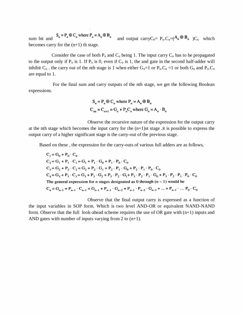
sum bit and and output carryC0= Pn.Cn=( )Cn which
becomes carry for the (n+1) th stage.
Consider the case of both Pn and Cn being 1. The input carry Cn has to be propagated
to the output only if Pn is 1. If Pn is 0, even if Cn is 1, the and gate in the second half-adder will
inhibit Cn . the carry out of the nth stage is 1 when either Gn=1 or Pn.Cn =1 or both Gn and Pn.Cn
are equal to 1.
For the final sum and carry outputs of the nth stage, we get the following Boolean
expressions.
Observe the recursive nature of the expression for the output carry
at the nth stage which becomes the input carry for the (n+1)st stage .it is possible to express the
output carry of a higher significant stage is the carry-out of the previous stage.
Based on these , the expression for the carry-outs of various full adders are as follows,
Observe that the final output carry is expressed as a function of
the input variables in SOP form. Which is two level AND-OR or equivalent NAND-NAND
form. Observe that the full look-ahead scheme requires the use of OR gate with (n+1) inputs and
AND gates with number of inputs varying from 2 to (n+1).
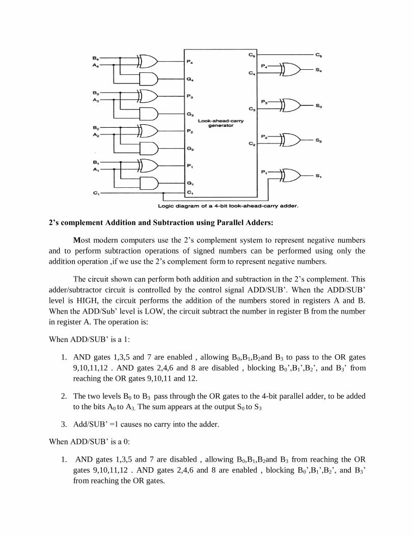
2’s complement Addition and Subtraction using Parallel Adders:
Most modern computers use the 2‘s complement system to represent negative numbers
and to perform subtraction operations of signed numbers can be performed using only the
addition operation ,if we use the 2‘s complement form to represent negative numbers.
The circuit shown can perform both addition and subtraction in the 2‘s complement. This
adder/subtractor circuit is controlled by the control signal ADD/SUB‘. When the ADD/SUB‘
level is HIGH, the circuit performs the addition of the numbers stored in registers A and B.
When the ADD/Sub‘ level is LOW, the circuit subtract the number in register B from the number
in register A. The operation is:
When ADD/SUB‘ is a 1:
1. AND gates 1,3,5 and 7 are enabled , allowing B0,B1,B2and B3 to pass to the OR gates
9,10,11,12 . AND gates 2,4,6 and 8 are disabled , blocking B0‘,B1‘,B2‘, and B3‘ from
reaching the OR gates 9,10,11 and 12.
2. The two levels B0 to B3 pass through the OR gates to the 4-bit parallel adder, to be added
to the bits A0 to A3. The sum appears at the output S0 to S3
3. Add/SUB‘ =1 causes no carry into the adder.
When ADD/SUB‘ is a 0:
1. AND gates 1,3,5 and 7 are disabled , allowing B0,B1,B2and B3 from reaching the OR
gates 9,10,11,12 . AND gates 2,4,6 and 8 are enabled , blocking B0‘,B1‘,B2‘, and B3‘
from reaching the OR gates.
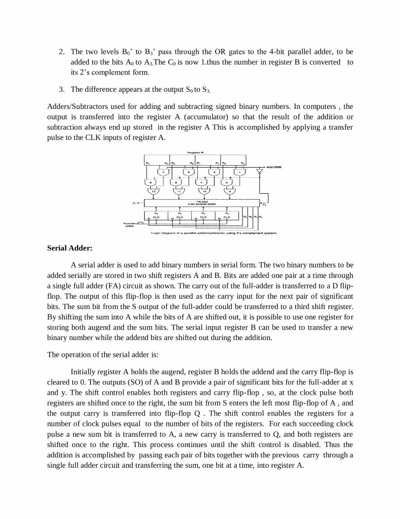
2. The two levels B0‘ to B3‘ pass through the OR gates to the 4-bit parallel adder, to be
added to the bits A0 to A3.The C0 is now 1.thus the number in register B is converted to
its 2‘s complement form.
3. The difference appears at the output S0 to S3.
Adders/Subtractors used for adding and subtracting signed binary numbers. In computers , the
output is transferred into the register A (accumulator) so that the result of the addition or
subtraction always end up stored in the register A This is accomplished by applying a transfer
pulse to the CLK inputs of register A.
Serial Adder:
A serial adder is used to add binary numbers in serial form. The two binary numbers to be
added serially are stored in two shift registers A and B. Bits are added one pair at a time through
a single full adder (FA) circuit as shown. The carry out of the full-adder is transferred to a D flip-
flop. The output of this flip-flop is then used as the carry input for the next pair of significant
bits. The sum bit from the S output of the full-adder could be transferred to a third shift register.
By shifting the sum into A while the bits of A are shifted out, it is possible to use one register for
storing both augend and the sum bits. The serial input register B can be used to transfer a new
binary number while the addend bits are shifted out during the addition.
The operation of the serial adder is:
Initially register A holds the augend, register B holds the addend and the carry flip-flop is
cleared to 0. The outputs (SO) of A and B provide a pair of significant bits for the full-adder at x
and y. The shift control enables both registers and carry flip-flop , so, at the clock pulse both
registers are shifted once to the right, the sum bit from S enters the left most flip-flop of A , and
the output carry is transferred into flip-flop Q . The shift control enables the registers for a
number of clock pulses equal to the number of bits of the registers. For each succeeding clock
pulse a new sum bit is transferred to A, a new carry is transferred to Q, and both registers are
shifted once to the right. This process continues until the shift control is disabled. Thus the
addition is accomplished by passing each pair of bits together with the previous carry through a
single full adder circuit and transferring the sum, one bit at a time, into register A.
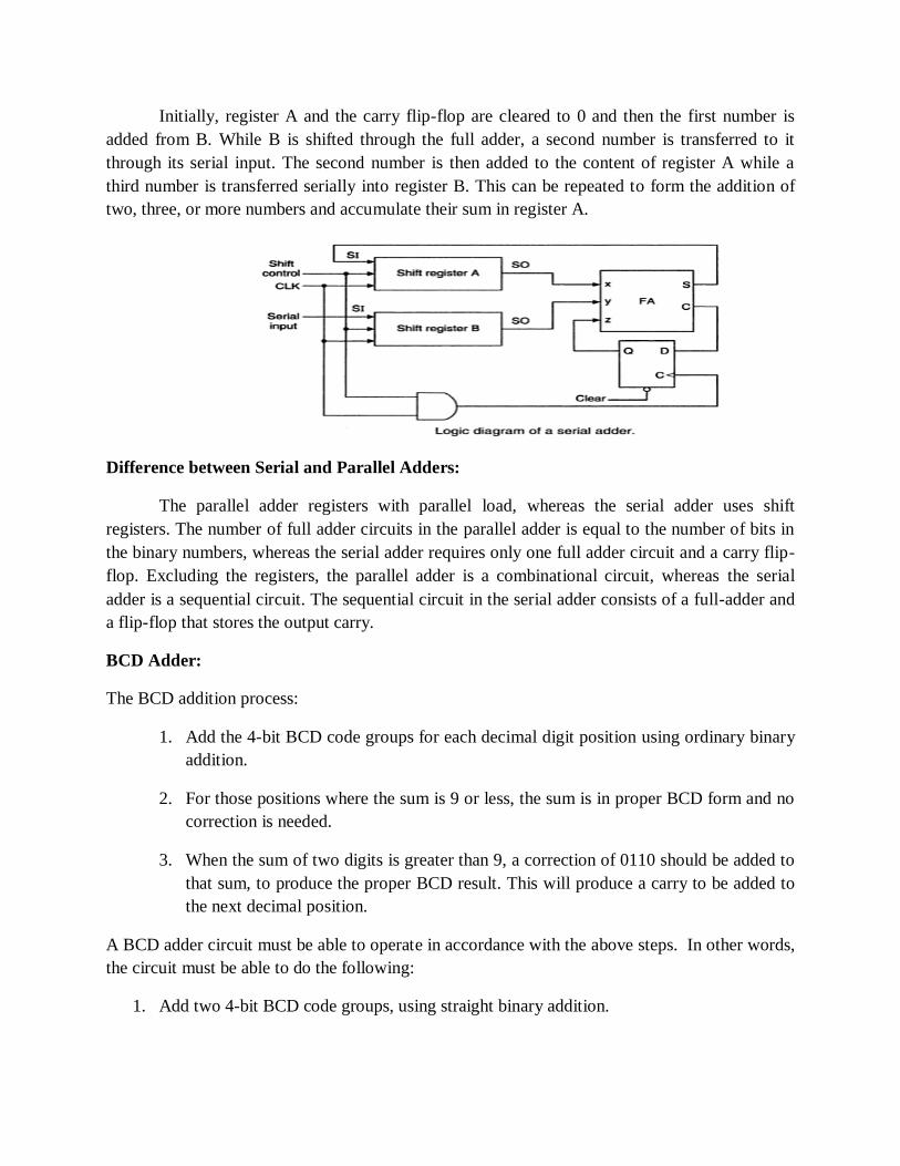
Initially, register A and the carry flip-flop are cleared to 0 and then the first number is
added from B. While B is shifted through the full adder, a second number is transferred to it
through its serial input. The second number is then added to the content of register A while a
third number is transferred serially into register B. This can be repeated to form the addition of
two, three, or more numbers and accumulate their sum in register A.
Difference between Serial and Parallel Adders:
The parallel adder registers with parallel load, whereas the serial adder uses shift
registers. The number of full adder circuits in the parallel adder is equal to the number of bits in
the binary numbers, whereas the serial adder requires only one full adder circuit and a carry flip-
flop. Excluding the registers, the parallel adder is a combinational circuit, whereas the serial
adder is a sequential circuit. The sequential circuit in the serial adder consists of a full-adder and
a flip-flop that stores the output carry.
BCD Adder:
The BCD addition process:
1. Add the 4-bit BCD code groups for each decimal digit position using ordinary binary
addition.
2. For those positions where the sum is 9 or less, the sum is in proper BCD form and no
correction is needed.
3. When the sum of two digits is greater than 9, a correction of 0110 should be added to
that sum, to produce the proper BCD result. This will produce a carry to be added to
the next decimal position.
A BCD adder circuit must be able to operate in accordance with the above steps. In other words,
the circuit must be able to do the following:
1. Add two 4-bit BCD code groups, using straight binary addition.
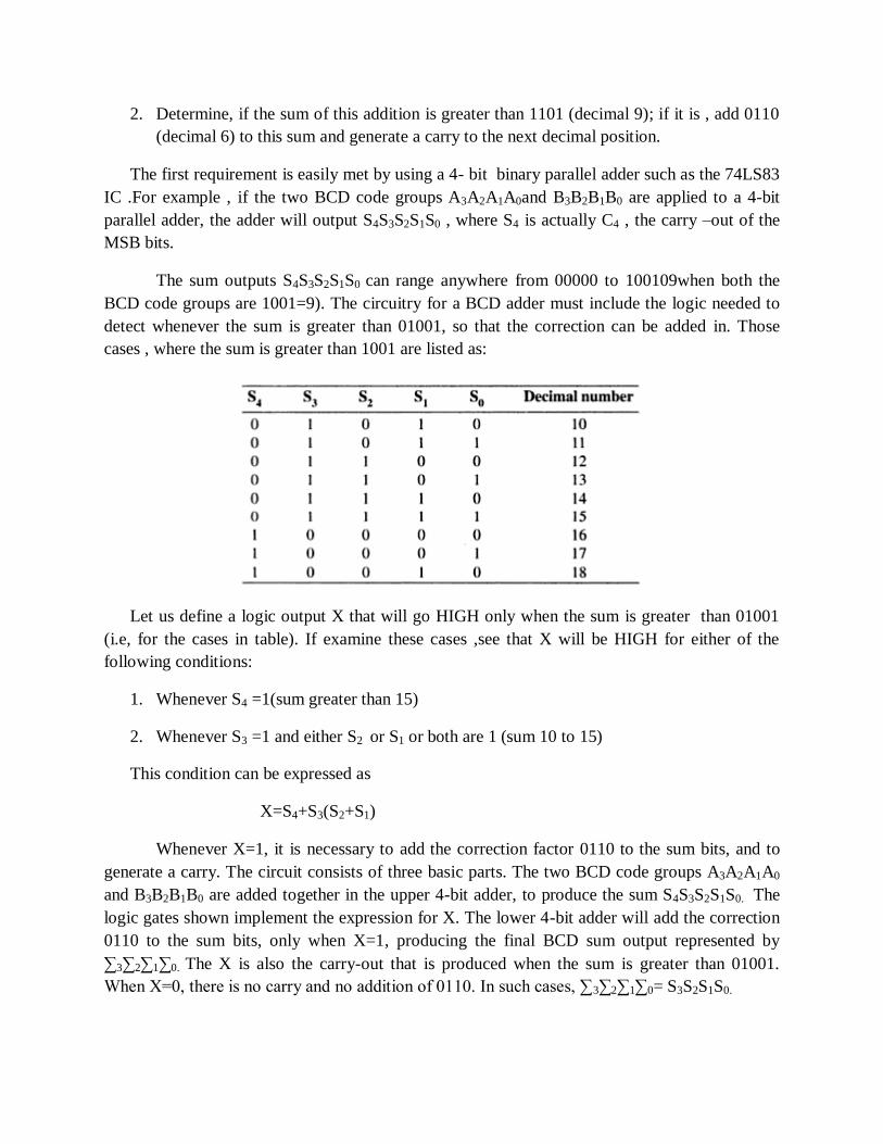
2. Determine, if the sum of this addition is greater than 1101 (decimal 9); if it is , add 0110
(decimal 6) to this sum and generate a carry to the next decimal position.
The first requirement is easily met by using a 4- bit binary parallel adder such as the 74LS83
IC .For example , if the two BCD code groups A3A2A1A0and B3B2B1B0 are applied to a 4-bit
parallel adder, the adder will output S4S3S2S1S0 , where S4 is actually C4 , the carry –out of the
MSB bits.
The sum outputs S4S3S2S1S0 can range anywhere from 00000 to 100109when both the
BCD code groups are 1001=9). The circuitry for a BCD adder must include the logic needed to
detect whenever the sum is greater than 01001, so that the correction can be added in. Those
cases , where the sum is greater than 1001 are listed as:
Let us define a logic output X that will go HIGH only when the sum is greater than 01001
(i.e, for the cases in table). If examine these cases ,see that X will be HIGH for either of the
following conditions:
1. Whenever S4 =1(sum greater than 15)
2. Whenever S3 =1 and either S2 or S1 or both are 1 (sum 10 to 15)
This condition can be expressed as
X=S4+S3(S2+S1)
Whenever X=1, it is necessary to add the correction factor 0110 to the sum bits, and to
generate a carry. The circuit consists of three basic parts. The two BCD code groups A3A2A1A0
and B3B2B1B0 are added together in the upper 4-bit adder, to produce the sum S4S3S2S1S0. The
logic gates shown implement the expression for X. The lower 4-bit adder will add the correction
0110 to the sum bits, only when X=1, producing the final BCD sum output represented by
∑3∑2∑1∑0. The X is also the carry-out that is produced when the sum is greater than 01001.
When X=0, there is no carry and no addition of 0110. In such cases, ∑3∑2∑1∑0= S3S2S1S0.
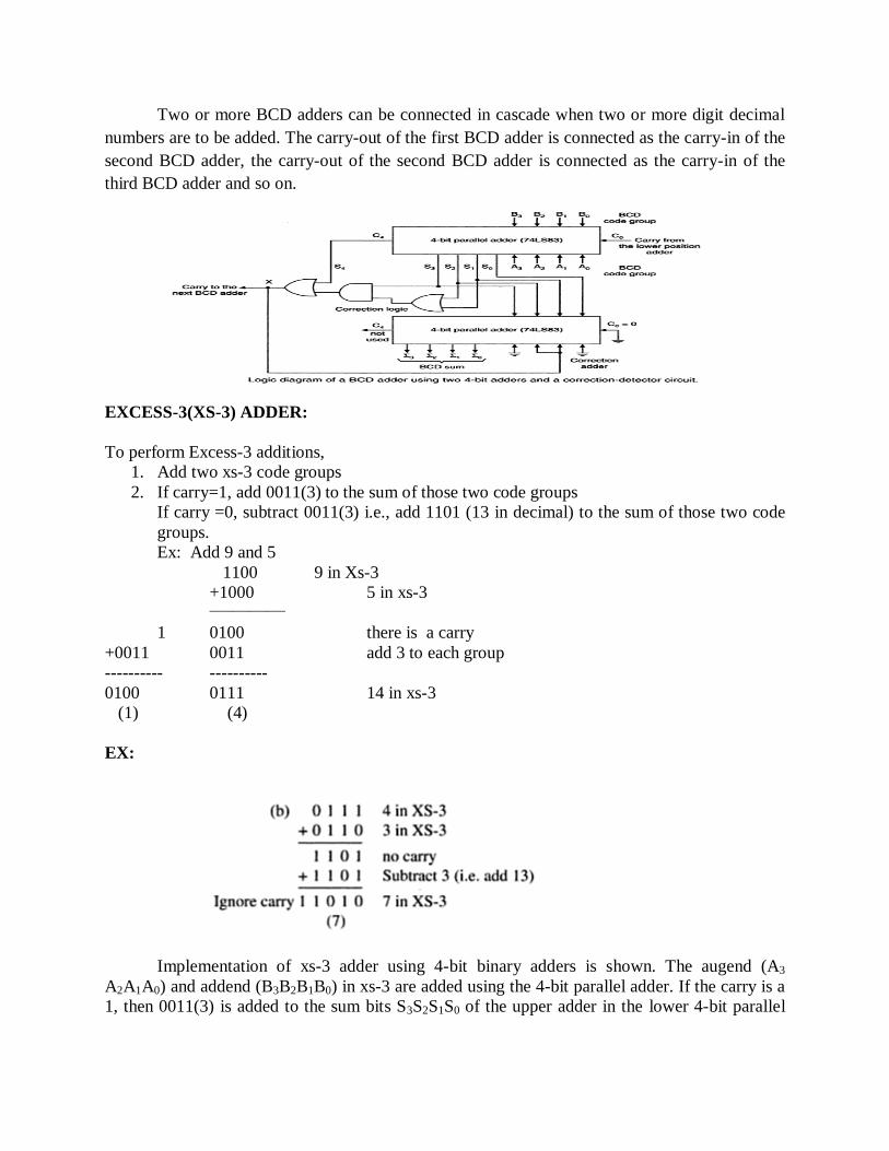
Two or more BCD adders can be connected in cascade when two or more digit decimal
numbers are to be added. The carry-out of the first BCD adder is connected as the carry-in of the
second BCD adder, the carry-out of the second BCD adder is connected as the carry-in of the
third BCD adder and so on.
EXCESS-3(XS-3) ADDER:
To perform Excess-3 additions,
1. Add two xs-3 code groups
2. If carry=1, add 0011(3) to the sum of those two code groups
If carry =0, subtract 0011(3) i.e., add 1101 (13 in decimal) to the sum of those two code
groups.
Ex: Add 9 and 5
1100 9 in Xs-3
+1000 5 in xs-3 _____________
1 0100 there is a carry
+0011 0011 add 3 to each group
---------- ----------
0100 0111 14 in xs-3
(1) (4)
EX:
Implementation of xs-3 adder using 4-bit binary adders is shown. The augend (A3
A2A1A0) and addend (B3B2B1B0) in xs-3 are added using the 4-bit parallel adder. If the carry is a
1, then 0011(3) is added to the sum bits S3S2S1S0 of the upper adder in the lower 4-bit parallel
adder. If the carry is a 0, then 1101(3) is added to the sum bits (This is equivalent to subtracting
0011(3) from the sum bits. The correct sum in xs-3 is obtained
Excess-3 (XS-3) Subtractor:
To perform Excess-3 subtraction,
1. Complement the subtrahend
2. Add the complemented subtrahend to the minuend.
3. If carry =1, result is positive. Add 3 and end around carry to the result . If carry=0, the
result is negative. Subtract 3, i.e, and take the 1‘s complement of the result.
Ex: Perform 9-4
1100 9 in xs-3
+1000 Complement of 4 n Xs-3
--------
(1) 0100 There is a carry
+0011 Add 0011(3)
------------
0111
1 End around carry
------------
1000 5 in xs-3
The minuend and the 1‘s complement of the subtrahend in xs-3 are added in the upper 4-
bit parallel adder. If the carry-out from the upper adder is a 0, then 1101 is added to the sum bits
of the upper adder in the lower adder and the sum bits of the lower adder are complemented to
get the result. If the carry-out from the upper adder is a 1, then 3=0011 is added to the sum bits
of the lower adder and the sum bits of the lower adder give the result.
Binary Multipliers:
In binary multiplication by the paper and pencil method, is modified somewhat in digital
machines because a binary adder can add only two binary numbers at a time.
In a binary multiplier, instead of adding all the partial products at the end, they are added two at
a time and their sum accumulated in a register (the accumulator register). In addition, when the
multiplier bit is a 0,0s are not written down and added because it does not affect the final result.
Instead, the multiplicand is shifted left by one bit.
The multiplication of 1110 by 1001 using this process is
Multiplicand 1110
Multiplier 1001
1110 The LSB of the multiplier is a 1; write down the
multiplicand; shift the multiplicand one position to the left
(1 1 1 0 0 )
1110 The second multiplier bit is a 0; write down the previous
result 1110; shift the multiplicand to the left again (1 1 1 0
0 0)
+1110000 The fourth multiplier bit is a 1 write down the new
multiplicand add it to the first partial product to obtain the
final product.
1111110
This multiplication process can be performed by the serial multiplier circuit , which
multiplies two 4-bit numbers to produce an 8-bit product. The circuit consists of following
elements
X register: A 4-bit shift register that stores the multiplier --- it will shift right on the falling edge
of the clock. Note that 0s are shifted in from the left.
B register: An 8-bit register that stores the multiplicand; it will shift left on the falling edge of
the clock. Note that 0s are shifted in from the right.
A register: An 8-bit register, i.e, the accumulator that accumulates the partial products.
Adder:An 8-bit parallel adder that produces the sum of A and B registers. The adder outputs S7
through S0 are connected to the D inputs of the accumulator so that the sum can be transferred to
the accumulator only when a clock pulse gets through the AND gate.
The circuit operation can be described by going through each step in the multiplication of 1110
by 1001. The complete process requires 4 clock cycles.
1. Before the first clock pulse: Prior to the occurrence of the first clock pulse, the register A is
loaded with 00000000, the register B with the multiplicand 00001110, and the register X with
the multiplier 1001. Assume that each of these registers is loaded using its asynchronous
inputs(i.e., PRESET and CLEAR). The output of the adder will be the sum of A and B,i.e.,
00001110.
2. First Clock pulse:Since the LSB of the multiplier (X0) is a 1, the first clock pulse gets
through the AND gate and its positive going transition transfers the sum outputs into the
accumulator. The subsequent negative going transition causes the X and B registers to shift right
and left, respectively. This produces a new sum of A and B.
3. Second Clock Pulse: The second bit of the original multiplier is now in X0 . Since this bit is a
0, the second clock pulse is inhibited from reaching the accumulator. Thus, the sum outputs are
not transferred into the accumulator and the number in the accumulator does not change. The
negative going transition of the clock pulse will again shift the X and B registers. Again a new
sum is produced.
4. Third Clock Pulse:The third bit of the original multiplier is now in X0;since this bit is a 0, the
third clock pulse is inhibited from reaching the accumulator. Thus, the sum outputs are not
transferred into the accumulator and the number in the accumulator does not change. The
negative going transition of the clock pulse will again shift the X and B registers. Again a new
sum is produced.
5.Fourth Clock Pulse: The last bit of the original multiplier is now in X0 , and since it is a 1, the
positive going transition of the fourth pulse transfers the sum into the accumulator. The
accumulator now holds the final product. The negative going transition of the clock pulse shifts
X and B again. Note that, X is now 0000, since all the multiplier bits have been shifted out.
Code converters:
The availability of a large variety of codes for the same discrete elements of
information results in the use of different codes by different digital systems. It is sometimes
necessary to use the output of one system as the input to another. A conversion circuit must be
inserted between the two systems if each uses different codes for the same information. Thus a
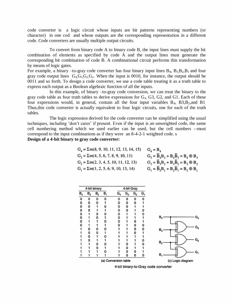
code converter is a logic circuit whose inputs are bit patterns representing numbers (or
character) in one cod and whose outputs are the corresponding representation in a different
code. Code converters are usually multiple output circuits.
To convert from binary code A to binary code B, the input lines must supply the bit
combination of elements as specified by code A and the output lines must generate the
corresponding bit combination of code B. A combinational circuit performs this transformation
by means of logic gates.
For example, a binary –to-gray code converter has four binary input lines B4, B3,B2,B1 and four
gray code output lines G4,G3,G2,G1. When the input is 0010, for instance, the output should be
0011 and so forth. To design a code converter, we use a code table treating it as a truth table to
express each output as a Boolean algebraic function of all the inputs.
In this example, of binary –to-gray code conversion, we can treat the binary to the
gray code table as four truth tables to derive expressions for G4, G3, G2, and G1. Each of these
four expressions would, in general, contain all the four input variables B4, B3,B2,and B1.
Thus,this code converter is actually equivalent to four logic circuits, one for each of the truth
tables.
The logic expression derived for the code converter can be simplified using the usual
techniques, including ‗don‘t cares‘ if present. Even if the input is an unweighted code, the same
cell numbering method which we used earlier can be used, but the cell numbers --must
correspond to the input combinations as if they were an 8-4-2-1 weighted code. s
Design of a 4-bit binary to gray code converter:
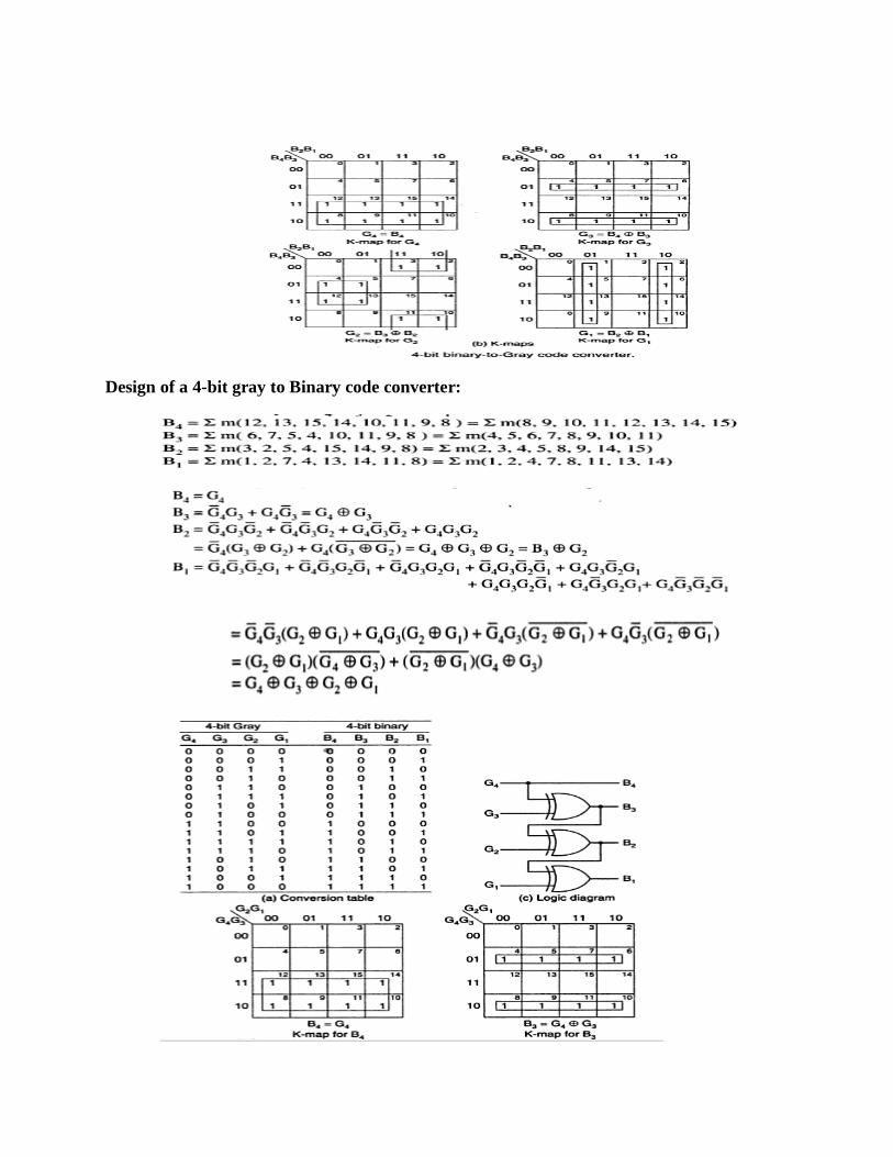
Design of a 4-bit gray to Binary code converter:
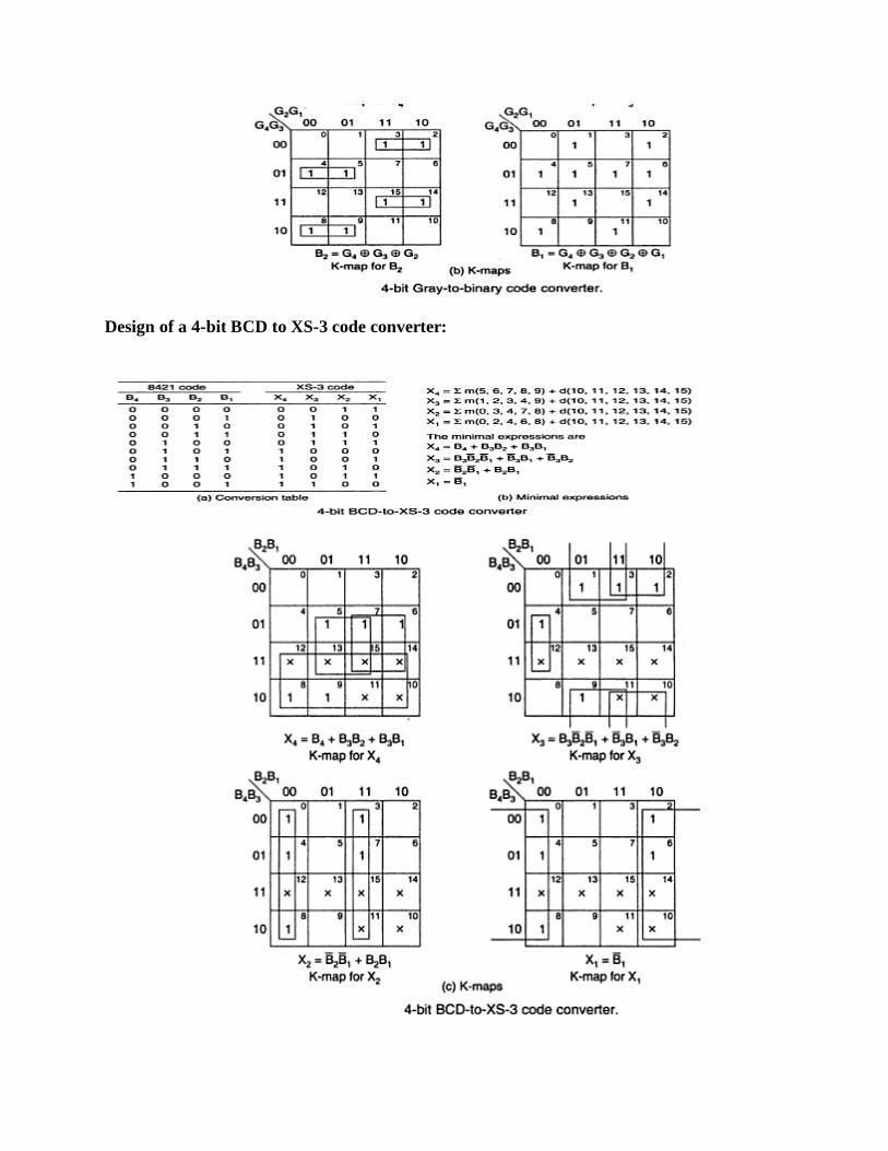
Design of a 4-bit BCD to XS-3 code converter:
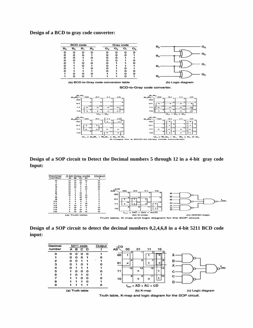
Design of a BCD to gray code converter:
Design of a SOP circuit to Detect the Decimal numbers 5 through 12 in a 4-bit gray code
Input:
Design of a SOP circuit to detect the decimal numbers 0,2,4,6,8 in a 4-bit 5211 BCD code
input:
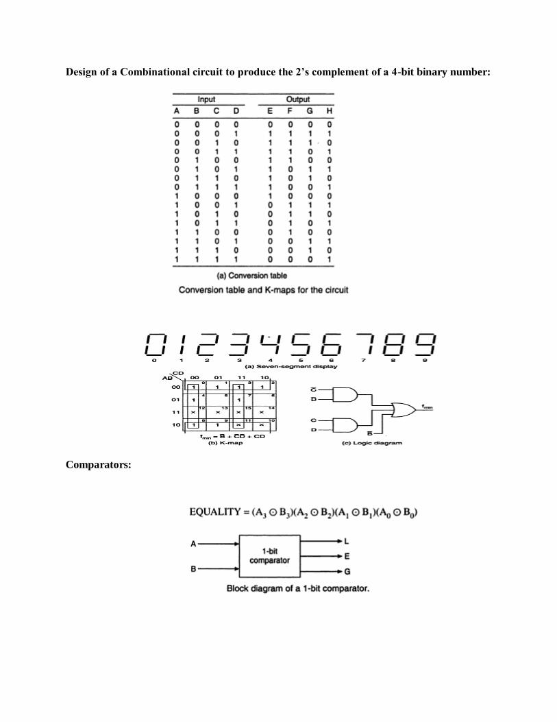
Design of a Combinational circuit to produce the 2’s complement of a 4-bit binary number:
Comparators:
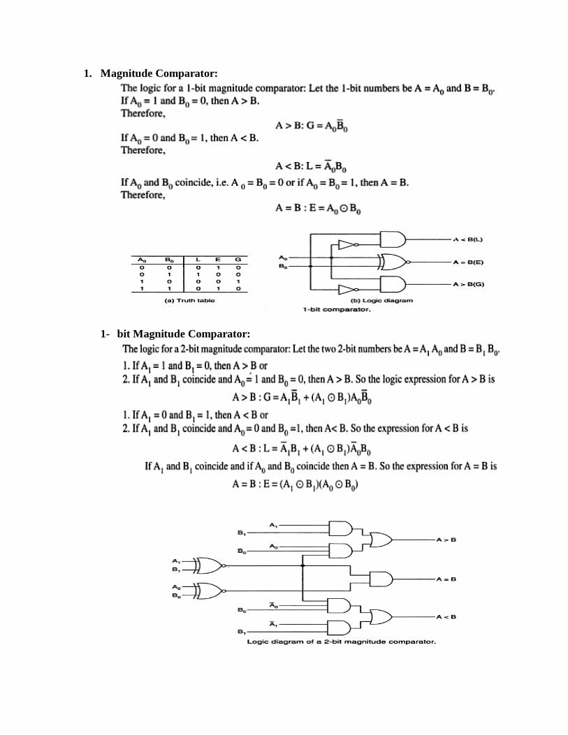
1. Magnitude Comparator:
1- bit Magnitude Comparator:
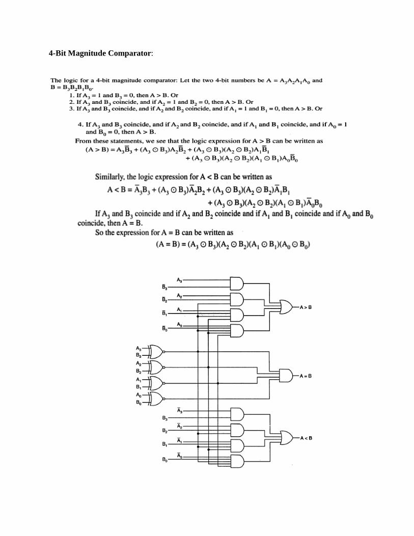
4-Bit Magnitude Comparator:
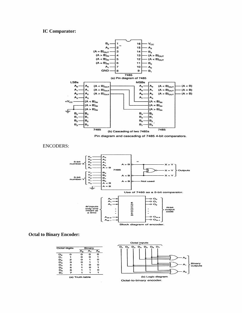
IC Comparator:
ENCODERS:
Octal to Binary Encoder:
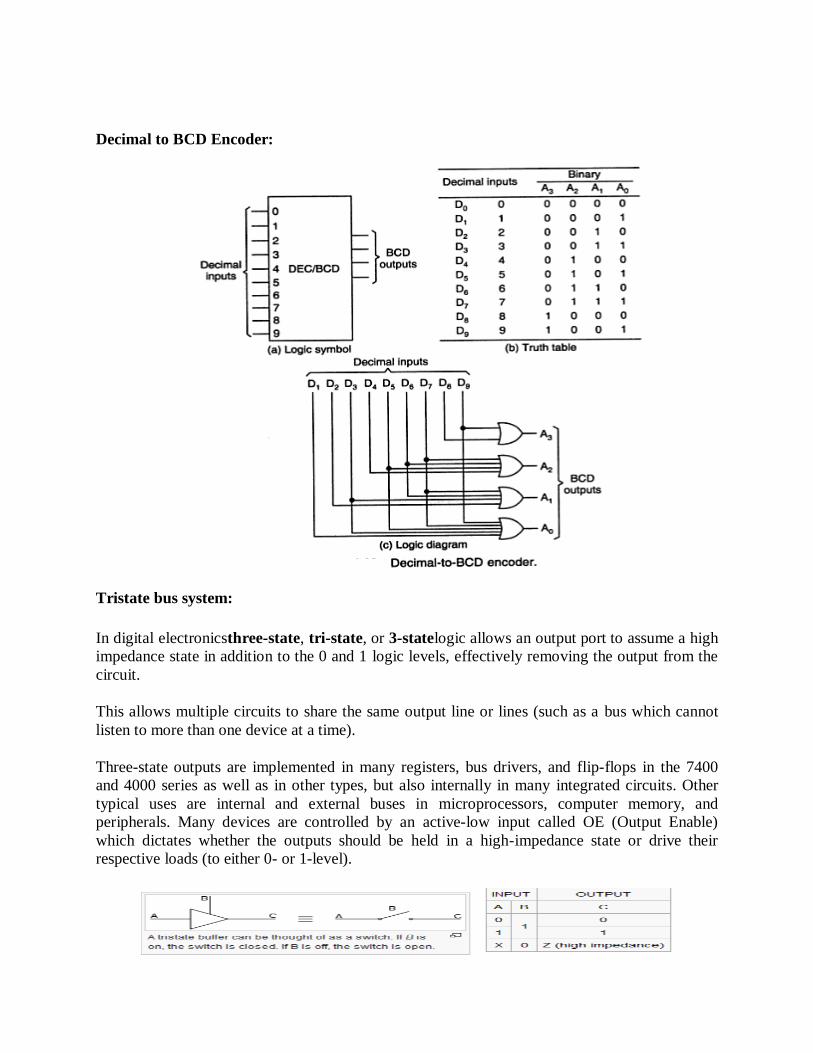
Decimal to BCD Encoder:
Tristate bus system:
In digital electronicsthree-state, tri-state, or 3-statelogic allows an output port to assume a high
impedance state in addition to the 0 and 1 logic levels, effectively removing the output from the
circuit.
This allows multiple circuits to share the same output line or lines (such as a bus which cannot
listen to more than one device at a time).
Three-state outputs are implemented in many registers, bus drivers, and flip-flops in the 7400
and 4000 series as well as in other types, but also internally in many integrated circuits. Other
typical uses are internal and external buses in microprocessors, computer memory, and
peripherals. Many devices are controlled by an active-low input called OE (Output Enable)
which dictates whether the outputs should be held in a high-impedance state or drive their
respective loads (to either 0- or 1-level).
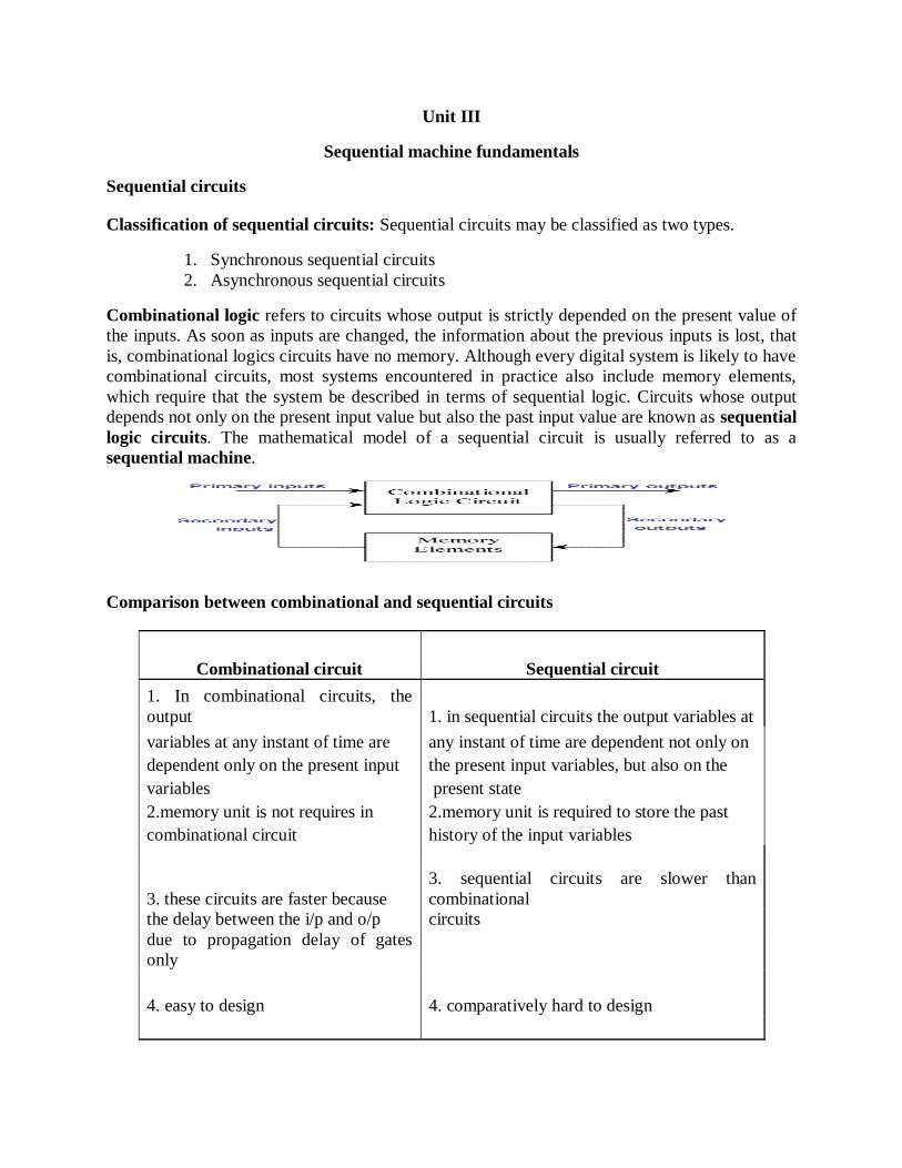
Unit III
Sequential machine fundamentals
Sequential circuits
Classification of sequential circuits: Sequential circuits may be classified as two types.
1. Synchronous sequential circuits
2. Asynchronous sequential circuits
Combinational logic refers to circuits whose output is strictly depended on the present value of
the inputs. As soon as inputs are changed, the information about the previous inputs is lost, that
is, combinational logics circuits have no memory. Although every digital system is likely to have
combinational circuits, most systems encountered in practice also include memory elements,
which require that the system be described in terms of sequential logic. Circuits whose output
depends not only on the present input value but also the past input value are known as sequential
logic circuits. The mathematical model of a sequential circuit is usually referred to as a
sequential machine.
Comparison between combinational and sequential circuits
Combinational circuit Sequential circuit
1. In combinational circuits, the
output 1. in sequential circuits the output variables at
variables at any instant of time are any instant of time are dependent not only on
dependent only on the present input the present input variables, but also on the
variables present state
2.memory unit is not requires in 2.memory unit is required to store the past
combinational circuit history of the input variables
3. these circuits are faster because
3. sequential circuits are slower than
combinational
the delay between the i/p and o/p circuits
due to propagation delay of gates
only
4. easy to design 4. comparatively hard to design
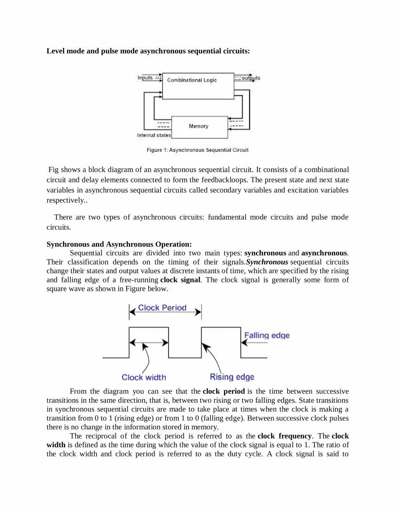
Level mode and pulse mode asynchronous sequential circuits:
Fig shows a block diagram of an asynchronous sequential circuit. It consists of a combinational
circuit and delay elements connected to form the feedbackloops. The present state and next state
variables in asynchronous sequential circuits called secondary variables and excitation variables
respectively..
There are two types of asynchronous circuits: fundamental mode circuits and pulse mode
circuits.
Synchronous and Asynchronous Operation: Sequential circuits are divided into two main types: synchronous and asynchronous.
Their classification depends on the timing of their signals.Synchronous sequential circuits
change their states and output values at discrete instants of time, which are specified by the rising
and falling edge of a free-running clock signal. The clock signal is generally some form of
square wave as shown in Figure below.
From the diagram you can see that the clock period is the time between successive
transitions in the same direction, that is, between two rising or two falling edges. State transitions
in synchronous sequential circuits are made to take place at times when the clock is making a
transition from 0 to 1 (rising edge) or from 1 to 0 (falling edge). Between successive clock pulses
there is no change in the information stored in memory.
The reciprocal of the clock period is referred to as the clock frequency. The clock
width is defined as the time during which the value of the clock signal is equal to 1. The ratio of
the clock width and clock period is referred to as the duty cycle. A clock signal is said to
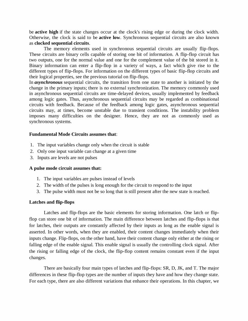
be active high if the state changes occur at the clock's rising edge or during the clock width.
Otherwise, the clock is said to be active low. Synchronous sequential circuits are also known
as clocked sequential circuits.
The memory elements used in synchronous sequential circuits are usually flip-flops.
These circuits are binary cells capable of storing one bit of information. A flip-flop circuit has
two outputs, one for the normal value and one for the complement value of the bit stored in it.
Binary information can enter a flip-flop in a variety of ways, a fact which give rise to the
different types of flip-flops. For information on the different types of basic flip-flop circuits and
their logical properties, see the previous tutorial on flip-flops.
In asynchronous sequential circuits, the transition from one state to another is initiated by the
change in the primary inputs; there is no external synchronization. The memory commonly used
in asynchronous sequential circuits are time-delayed devices, usually implemented by feedback
among logic gates. Thus, asynchronous sequential circuits may be regarded as combinational
circuits with feedback. Because of the feedback among logic gates, asynchronous sequential
circuits may, at times, become unstable due to transient conditions. The instability problem
imposes many difficulties on the designer. Hence, they are not as commonly used as
synchronous systems.
Fundamental Mode Circuits assumes that:
1. The input variables change only when the circuit is stable
2. Only one input variable can change at a given time
3. Inputs are levels are not pulses
A pulse mode circuit assumes that:
1. The input variables are pulses instead of levels
2. The width of the pulses is long enough for the circuit to respond to the input
3. The pulse width must not be so long that is still present after the new state is reached.
Latches and flip-flops
Latches and flip-flops are the basic elements for storing information. One latch or flip-
flop can store one bit of information. The main difference between latches and flip-flops is that
for latches, their outputs are constantly affected by their inputs as long as the enable signal is
asserted. In other words, when they are enabled, their content changes immediately when their
inputs change. Flip-flops, on the other hand, have their content change only either at the rising or
falling edge of the enable signal. This enable signal is usually the controlling clock signal. After
the rising or falling edge of the clock, the flip-flop content remains constant even if the input
changes.
There are basically four main types of latches and flip-flops: SR, D, JK, and T. The major
differences in these flip-flop types are the number of inputs they have and how they change state.
For each type, there are also different variations that enhance their operations. In this chapter, we
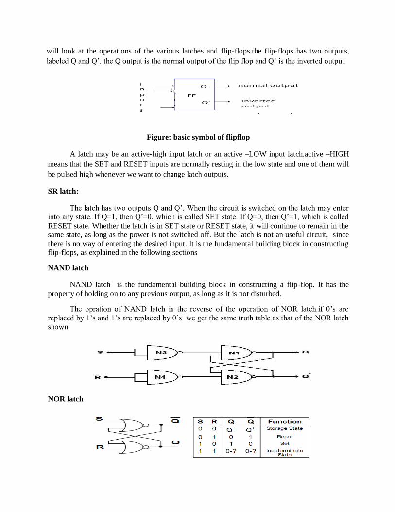
will look at the operations of the various latches and flip-flops.the flip-flops has two outputs,
labeled Q and Q‘. the Q output is the normal output of the flip flop and Q‘ is the inverted output.
Figure: basic symbol of flipflop
A latch may be an active-high input latch or an active –LOW input latch.active –HIGH
means that the SET and RESET inputs are normally resting in the low state and one of them will
be pulsed high whenever we want to change latch outputs.
SR latch:
The latch has two outputs Q and Q‘. When the circuit is switched on the latch may enter
into any state. If Q=1, then Q‘=0, which is called SET state. If Q=0, then Q‘=1, which is called
RESET state. Whether the latch is in SET state or RESET state, it will continue to remain in the
same state, as long as the power is not switched off. But the latch is not an useful circuit, since
there is no way of entering the desired input. It is the fundamental building block in constructing
flip-flops, as explained in the following sections
NAND latch
NAND latch is the fundamental building block in constructing a flip-flop. It has the
property of holding on to any previous output, as long as it is not disturbed.
The opration of NAND latch is the reverse of the operation of NOR latch.if 0‘s are
replaced by 1‘s and 1‘s are replaced by 0‘s we get the same truth table as that of the NOR latch
shown
NOR latch
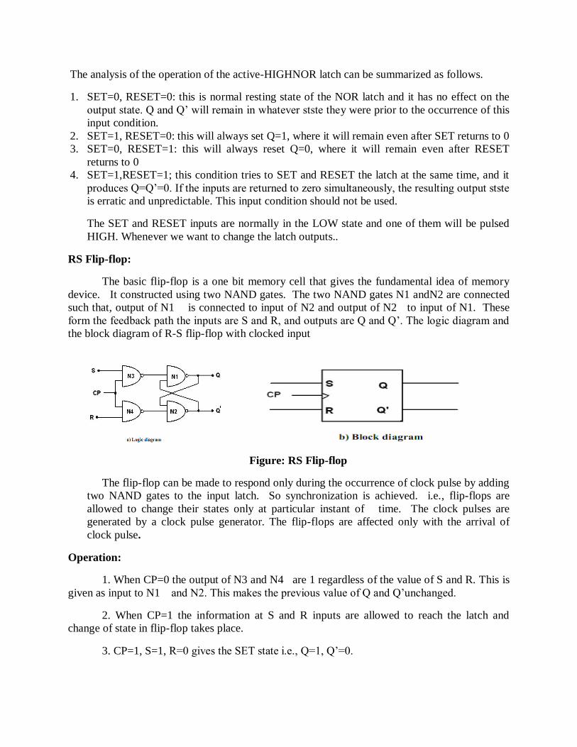
The analysis of the operation of the active-HIGHNOR latch can be summarized as follows.
1. SET=0, RESET=0: this is normal resting state of the NOR latch and it has no effect on the
output state. Q and Q‘ will remain in whatever stste they were prior to the occurrence of this
input condition.
2. SET=1, RESET=0: this will always set Q=1, where it will remain even after SET returns to 0
3. SET=0, RESET=1: this will always reset Q=0, where it will remain even after RESET
returns to 0
4. SET=1,RESET=1; this condition tries to SET and RESET the latch at the same time, and it
produces Q=Q‘=0. If the inputs are returned to zero simultaneously, the resulting output stste
is erratic and unpredictable. This input condition should not be used.
The SET and RESET inputs are normally in the LOW state and one of them will be pulsed
HIGH. Whenever we want to change the latch outputs..
RS Flip-flop:
The basic flip-flop is a one bit memory cell that gives the fundamental idea of memory
device. It constructed using two NAND gates. The two NAND gates N1 andN2 are connected
such that, output of N1 is connected to input of N2 and output of N2 to input of N1. These
form the feedback path the inputs are S and R, and outputs are Q and Q‘. The logic diagram and
the block diagram of R-S flip-flop with clocked input
Figure: RS Flip-flop
The flip-flop can be made to respond only during the occurrence of clock pulse by adding
two NAND gates to the input latch. So synchronization is achieved. i.e., flip-flops are
allowed to change their states only at particular instant of time. The clock pulses are
generated by a clock pulse generator. The flip-flops are affected only with the arrival of
clock pulse.
Operation:
1. When CP=0 the output of N3 and N4 are 1 regardless of the value of S and R. This is
given as input to N1 and N2. This makes the previous value of Q and Q‘unchanged.
2. When CP=1 the information at S and R inputs are allowed to reach the latch and
change of state in flip-flop takes place.
3. CP=1, S=1, R=0 gives the SET state i.e., Q=1, Q‘=0.
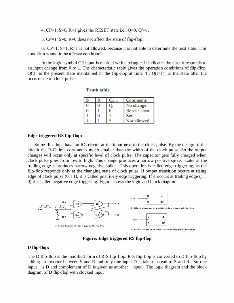
4. CP=1, S=0, R=1 gives the RESET state i.e., Q=0, Q‘=1.
5. CP=1, S=0, R=0 does not affect the state of flip-flop.
6. CP=1, S=1, R=1 is not allowed, because it is not able to determine the next state. This
condition is said to be a ―race condition‖.
In the logic symbol CP input is marked with a triangle. It indicates the circuit responds to
an input change from 0 to 1. The characteristic table gives the operation conditions of flip-flop.
Q(t) is the present state maintained in the flip-flop at time ‗t‘. Q(t+1) is the state after the
occurrence of clock pulse.
Edge triggered RS flip-flop:
Some flip-flops have an RC circuit at the input next to the clock pulse. By the design of the
circuit the R-C time constant is much smaller than the width of the clock pulse. So the output
changes will occur only at specific level of clock pulse. The capacitor gets fully charged when
clock pulse goes from low to high. This change produces a narrow positive spike. Later at the
trailing edge it produces narrow negative spike. This operation is called edge triggering, as the
flip-flop responds only at the changing state of clock pulse. If output transition occurs at rising
edge of clock pulse (01), it is called positively edge triggering. If it occurs at trailing edge (1
0) it is called negative edge triggering. Figure shows the logic and block diagram.
Figure: Edge triggered RS flip-flop
D flip-flop:
The D flip-flop is the modified form of R-S flip-flop. R-S flip-flop is converted to D flip-flop by
adding an inverter between S and R and only one input D is taken instead of S and R. So one
input is D and complement of D is given as another input. The logic diagram and the block
diagram of D flip-flop with clocked input
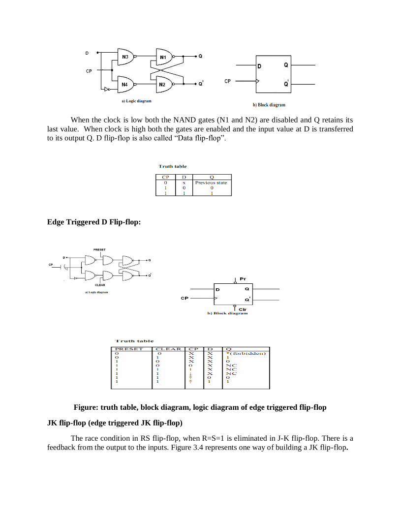
When the clock is low both the NAND gates (N1 and N2) are disabled and Q retains its
last value. When clock is high both the gates are enabled and the input value at D is transferred
to its output Q. D flip-flop is also called ―Data flip-flop‖.
Edge Triggered D Flip-flop:
Figure: truth table, block diagram, logic diagram of edge triggered flip-flop
JK flip-flop (edge triggered JK flip-flop)
The race condition in RS flip-flop, when R=S=1 is eliminated in J-K flip-flop. There is a
feedback from the output to the inputs. Figure 3.4 represents one way of building a JK flip-flop.
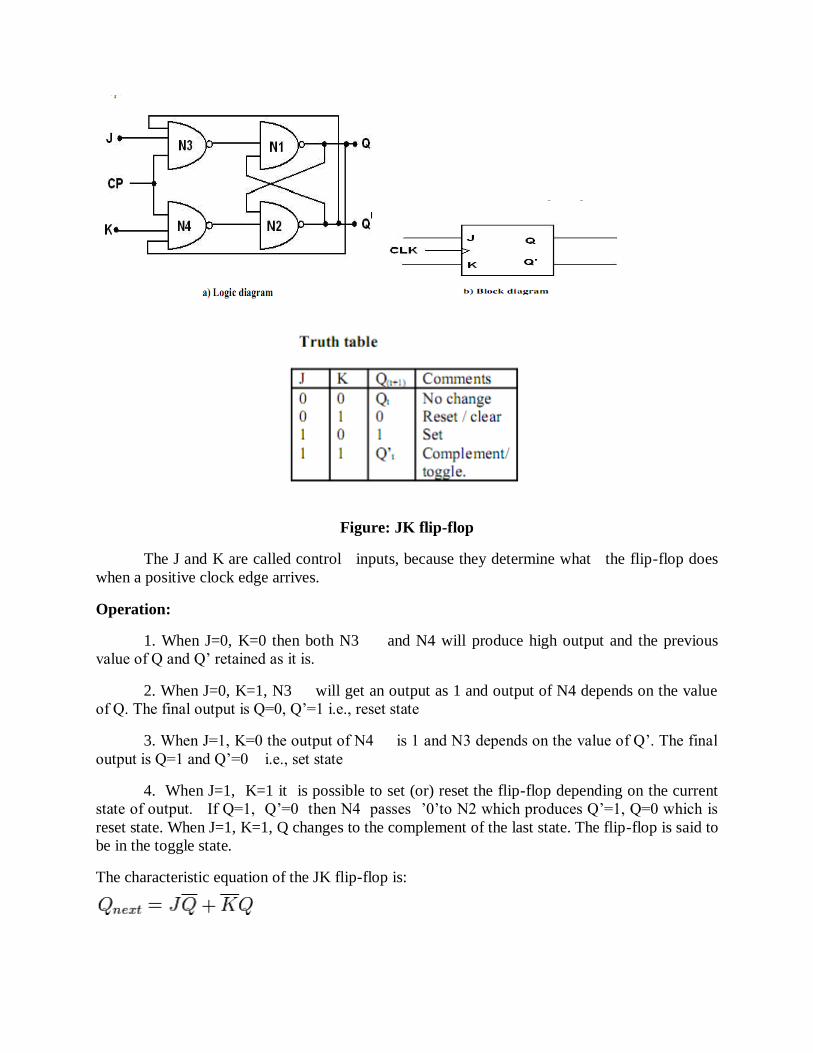
Figure: JK flip-flop
The J and K are called control inputs, because they determine what the flip-flop does
when a positive clock edge arrives.
Operation:
1. When J=0, K=0 then both N3 and N4 will produce high output and the previous
value of Q and Q‘ retained as it is.
2. When J=0, K=1, N3 will get an output as 1 and output of N4 depends on the value
of Q. The final output is Q=0, Q‘=1 i.e., reset state
3. When J=1, K=0 the output of N4 is 1 and N3 depends on the value of Q‘. The final
output is Q=1 and Q‘=0 i.e., set state
4. When J=1, K=1 it is possible to set (or) reset the flip-flop depending on the current
state of output. If Q=1, Q‘=0 then N4 passes ‘0‘to N2 which produces Q‘=1, Q=0 which is
reset state. When J=1, K=1, Q changes to the complement of the last state. The flip-flop is said to
be in the toggle state.
The characteristic equation of the JK flip-flop is:
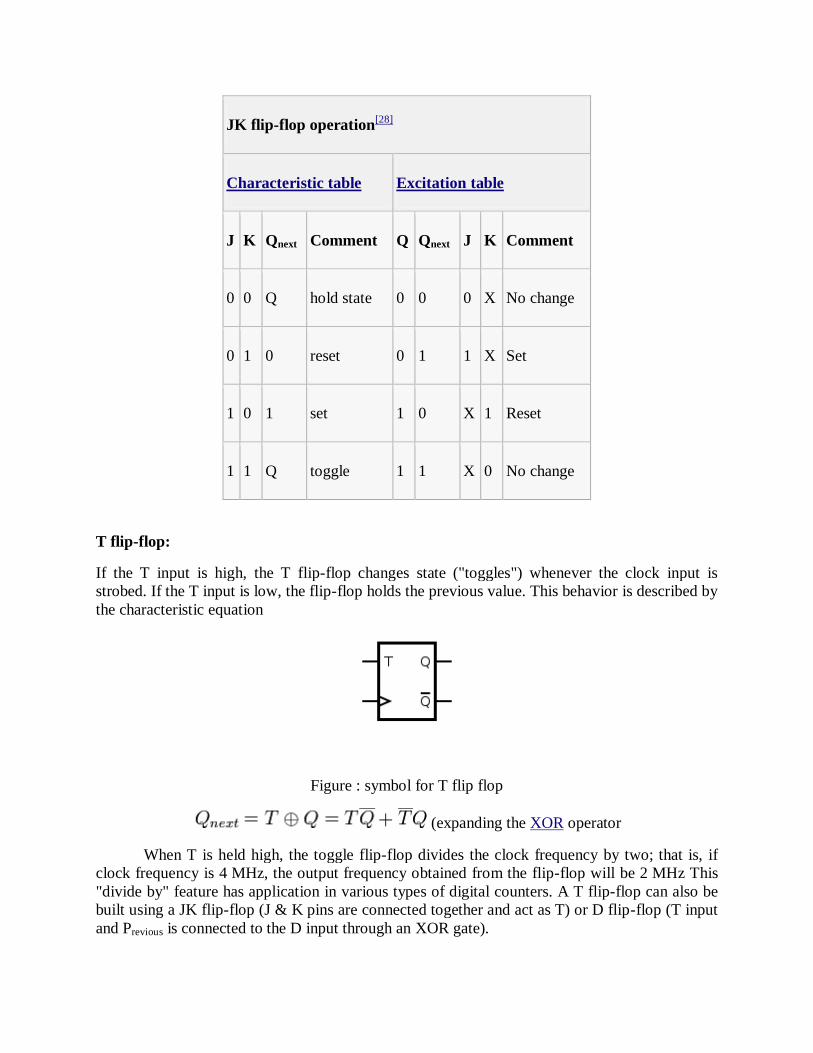
JK flip-flop operation[28]
Characteristic table Excitation table
J K Qnext Comment Q Qnext J K Comment
0 0 Q hold state 0 0 0 X No change
0 1 0 reset 0 1 1 X Set
1 0 1 set 1 0 X 1 Reset
1 1 Q toggle 1 1 X 0 No change
T flip-flop:
If the T input is high, the T flip-flop changes state ("toggles") whenever the clock input is
strobed. If the T input is low, the flip-flop holds the previous value. This behavior is described by
the characteristic equation
Figure : symbol for T flip flop
(expanding the XOR operator
When T is held high, the toggle flip-flop divides the clock frequency by two; that is, if
clock frequency is 4 MHz, the output frequency obtained from the flip-flop will be 2 MHz This
"divide by" feature has application in various types of digital counters. A T flip-flop can also be
built using a JK flip-flop (J & K pins are connected together and act as T) or D flip-flop (T input
and Previous is connected to the D input through an XOR gate).
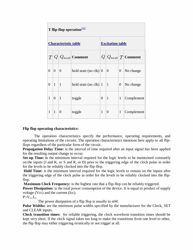
T flip-flop operation[28]
Characteristic table Excitation table
Comment
Comment
0 0 0 hold state (no clk) 0 0 0 No change
0 1 1 hold state (no clk) 1 1 0 No change
1 0 1 toggle 0 1 1 Complement
1 1 0 toggle 1 0 1 Complement
Flip flop operating characteristics:
The operation characteristics specify the performance, operating requirements, and
operating limitations of the circuits. The operation characteristics mentions here apply to all flip-
flops regardless of the particular form of the circuit.
Propagation Delay Time: is the interval of time required after an input signal has been applied
for the resulting output change to occur.
Set-up Time: is the minimum interval required for the logic levels to be maintained constantly
on the inputs (J and K, or S and R, or D) prior to the triggering edge of the clock pulse in order
for the levels to be reliably clocked into the flip-flop.
Hold Time: is the minimum interval required for the logic levels to remain on the inputs after
the triggering edge of the clock pulse in order for the levels to be reliably clocked into the flip-
flop.
Maximum Clock Frequency: is the highest rate that a flip-flop can be reliably triggered.
Power Dissipation: is the total power consumption of the device. It is equal to product of supply
voltage (Vcc) and the current (Icc).
P=Vcc.Icc
The power dissipation of a flip flop is usually in mW.
Pulse Widths: are the minimum pulse widths specified by the manufacturer for the Clock, SET
and CLEAR inputs.
Clock transition times: for reliable triggering, the clock waveform transition times should be
kept very short. If the clock signal takes too long to make the transitions from one level to other,
the flip flop may either triggering erratically or not trigger at all.
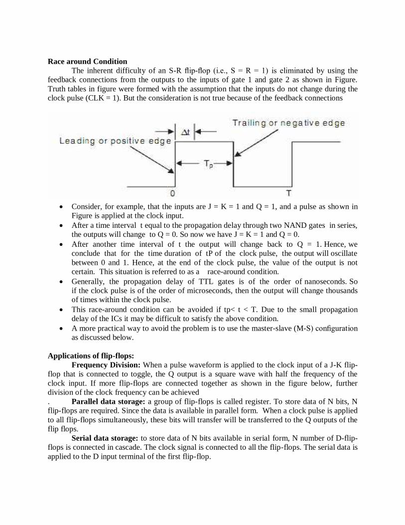
Race around Condition
The inherent difficulty of an S-R flip-flop (i.e., S = R = 1) is eliminated by using the
feedback connections from the outputs to the inputs of gate 1 and gate 2 as shown in Figure.
Truth tables in figure were formed with the assumption that the inputs do not change during the
clock pulse (CLK = 1). But the consideration is not true because of the feedback connections
Consider, for example, that the inputs are J = K = 1 and Q = 1, and a pulse as shown in
Figure is applied at the clock input.
After a time interval t equal to the propagation delay through two NAND gates in series,
the outputs will change to Q = 0. So now we have J = K = 1 and Q = 0.
After another time interval of t the output will change back to Q = 1. Hence, we
conclude that for the time duration of tP of the clock pulse, the output will oscillate
between 0 and 1. Hence, at the end of the clock pulse, the value of the output is not
certain. This situation is referred to as a race-around condition.
Generally, the propagation delay of TTL gates is of the order of nanoseconds. So
if the clock pulse is of the order of microseconds, then the output will change thousands
of times within the clock pulse.
This race-around condition can be avoided if tp< t < T. Due to the small propagation
delay of the ICs it may be difficult to satisfy the above condition.
A more practical way to avoid the problem is to use the master-slave (M-S) configuration
as discussed below.
Applications of flip-flops:
Frequency Division: When a pulse waveform is applied to the clock input of a J-K flip-
flop that is connected to toggle, the Q output is a square wave with half the frequency of the
clock input. If more flip-flops are connected together as shown in the figure below, further
division of the clock frequency can be achieved
. Parallel data storage: a group of flip-flops is called register. To store data of N bits, N
flip-flops are required. Since the data is available in parallel form. When a clock pulse is applied
to all flip-flops simultaneously, these bits will transfer will be transferred to the Q outputs of the
flip flops.
Serial data storage: to store data of N bits available in serial form, N number of D-flip-
flops is connected in cascade. The clock signal is connected to all the flip-flops. The serial data is
applied to the D input terminal of the first flip-flop.
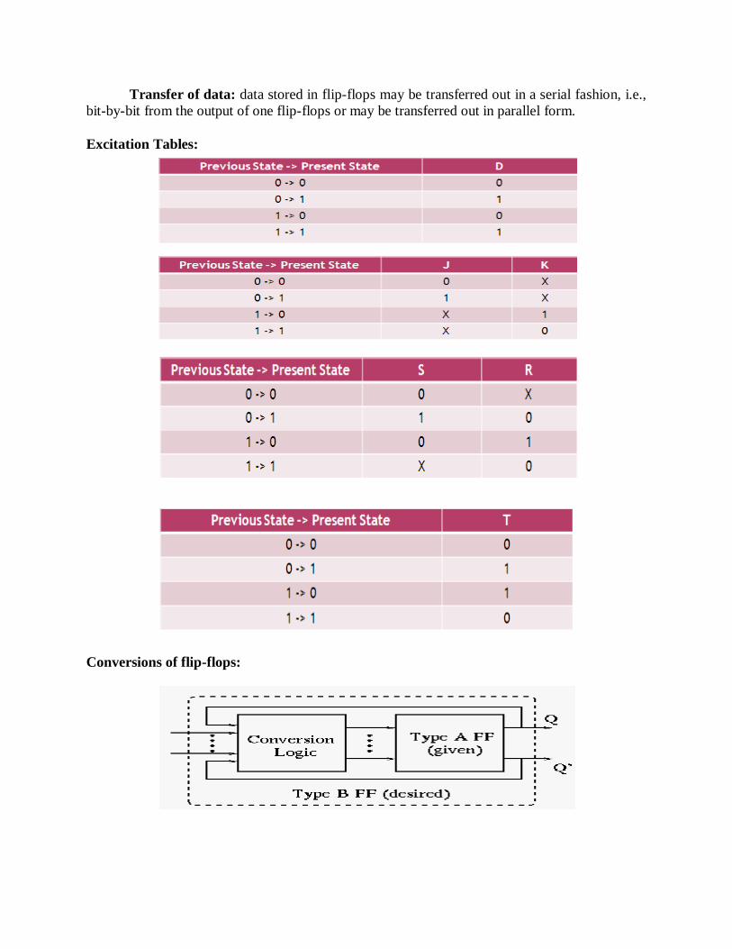
Transfer of data: data stored in flip-flops may be transferred out in a serial fashion, i.e.,
bit-by-bit from the output of one flip-flops or may be transferred out in parallel form.
Excitation Tables:
Conversions of flip-flops:
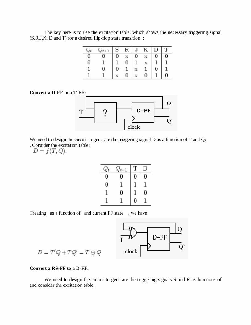
The key here is to use the excitation table, which shows the necessary triggering signal
(S,R,J,K, D and T) for a desired flip-flop state transition :
Convert a D-FF to a T-FF:
We need to design the circuit to generate the triggering signal D as a function of T and Q:
. Consider the excitation table:
Treating as a function of and current FF state , we have
Convert a RS-FF to a D-FF:
We need to design the circuit to generate the triggering signals S and R as functions of
and consider the excitation table:
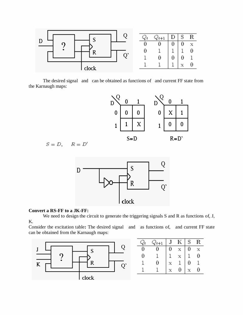
The desired signal and can be obtained as functions of and current FF state from
the Karnaugh maps:
Convert a RS-FF to a JK-FF:
We need to design the circuit to generate the triggering signals S and R as functions of, J,
K.
Consider the excitation table: The desired signal and as functions of, and current FF state
can be obtained from the Karnaugh maps:
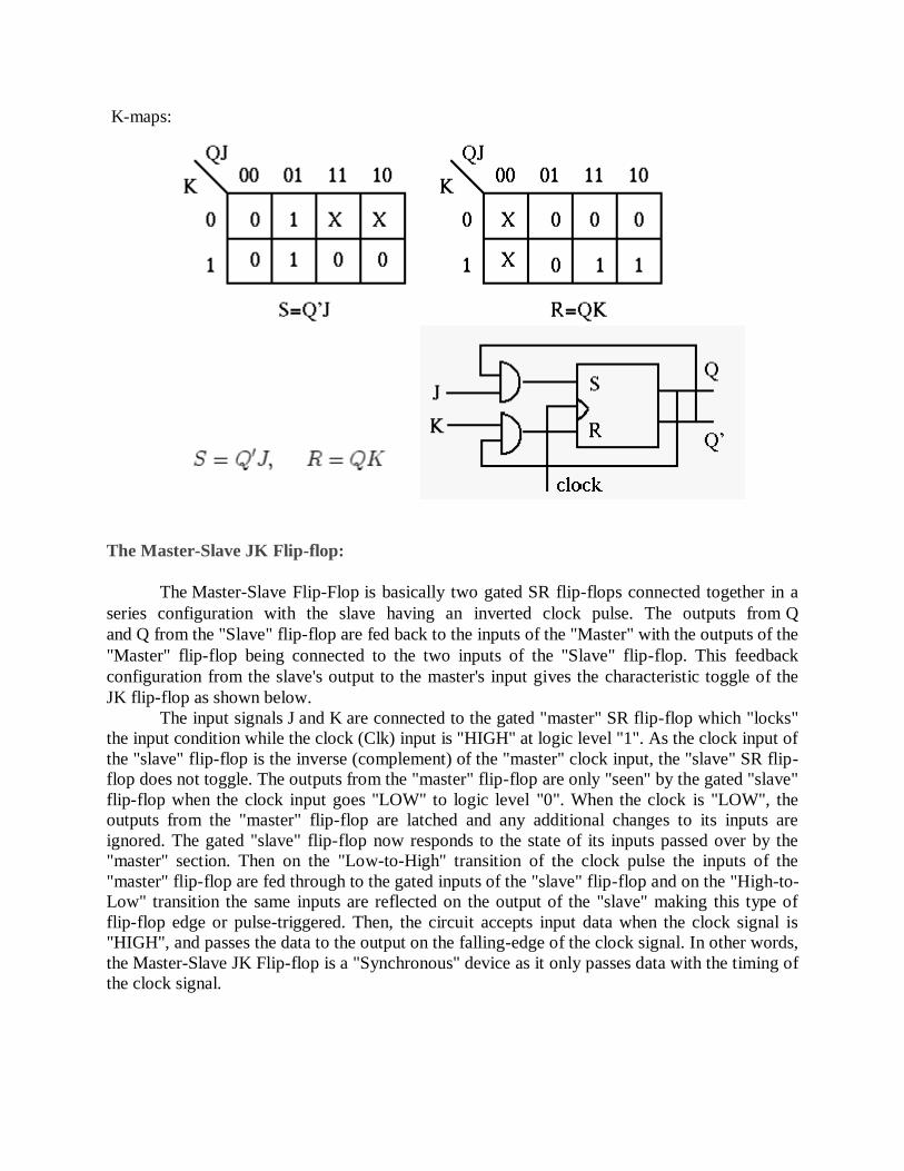
K-maps:
The Master-Slave JK Flip-flop:
The Master-Slave Flip-Flop is basically two gated SR flip-flops connected together in a
series configuration with the slave having an inverted clock pulse. The outputs from Q
and Q from the "Slave" flip-flop are fed back to the inputs of the "Master" with the outputs of the
"Master" flip-flop being connected to the two inputs of the "Slave" flip-flop. This feedback
configuration from the slave's output to the master's input gives the characteristic toggle of the
JK flip-flop as shown below.
The input signals J and K are connected to the gated "master" SR flip-flop which "locks"
the input condition while the clock (Clk) input is "HIGH" at logic level "1". As the clock input of
the "slave" flip-flop is the inverse (complement) of the "master" clock input, the "slave" SR flip-
flop does not toggle. The outputs from the "master" flip-flop are only "seen" by the gated "slave"
flip-flop when the clock input goes "LOW" to logic level "0". When the clock is "LOW", the
outputs from the "master" flip-flop are latched and any additional changes to its inputs are
ignored. The gated "slave" flip-flop now responds to the state of its inputs passed over by the
"master" section. Then on the "Low-to-High" transition of the clock pulse the inputs of the
"master" flip-flop are fed through to the gated inputs of the "slave" flip-flop and on the "High-to-
Low" transition the same inputs are reflected on the output of the "slave" making this type of
flip-flop edge or pulse-triggered. Then, the circuit accepts input data when the clock signal is
"HIGH", and passes the data to the output on the falling-edge of the clock signal. In other words,
the Master-Slave JK Flip-flop is a "Synchronous" device as it only passes data with the timing of
the clock signal.

UNIT 4
Sequential circuit design and analysis
Sequential Circuit Design
Steps in the design process for sequential circuits
State Diagrams and State Tables
Examples
Steps in Design of a Sequential Circuit
1. Specification – A description of the sequential circuit. Should include a detailing of the
inputs, the outputs, and the operation. Possibly assumes that you have knowledge of digital
system basics.
2. Formulation: Generate a state diagram and/or a state table from the statement of the problem.
3. State Assignment: From a state table assign binary codes to the states.
4. Flip-flop Input Equation Generation: Select the type of flip-flop for the circuit and generate
the needed input for the required state transitions
5. Output Equation Generation: Derive output logic equations for generation of the output from
the inputs and current state.
6. Optimization: Optimize the input and output equations. Today, CAD systems are typically
used for this in real systems.
7. Technology Mapping: Generate a logic diagram of the circuit using ANDs, ORs, Inverters,
and F/Fs.
8. Verification: Use a HDL to verify the design.
Mealy and Moore
Sequential machines are typically classified as either a Mealy machine or a Moore
machine implementation.
Moore machine: The outputs of the circuit depend only upon the current state of the
circuit.
Mealy machine: The outputs of the circuit depend upon both the current state of the
circuit and the inputs.
An example to go through the steps
The specification: The circuit will have one input, X, and one output, Z. The output Z will be 0
except when the input sequence 1101 are the last 4 inputs received on X. In that case it will be a
1
Generation of a state diagram
Create states and meaning for them.
State A – the last input was a 0 and previous inputs unknown. Can also be the reset state.
State B – the last input was a 1 and the previous input was a 0. The start of a new sequence
possibly.
Capture this in a state diagram
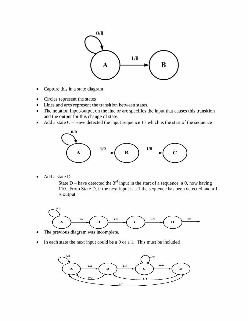
Capture this in a state diagram
Circles represent the states
Lines and arcs represent the transition between states.
The notation Input/output on the line or arc specifies the input that causes this transition
and the output for this change of state.
Add a state C – Have detected the input sequence 11 which is the start of the sequence
Add a state D
State D – have detected the 3rd
input in the start of a sequence, a 0, now having
110. From State D, if the next input is a 1 the sequence has been detected and a 1
is output.
The previous diagram was incomplete.
In each state the next input could be a 0 or a 1. This must be included
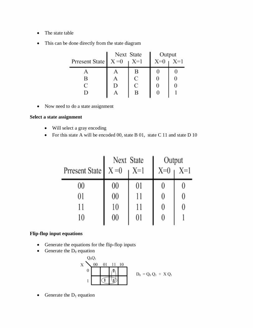
The state table
This can be done directly from the state diagram
Now need to do a state assignment
Select a state assignment
Will select a gray encoding
For this state A will be encoded 00, state B 01, state C 11 and state D 10
Flip-flop input equations
Generate the equations for the flip-flop inputs
Generate the D0 equation
Generate the D1 equation
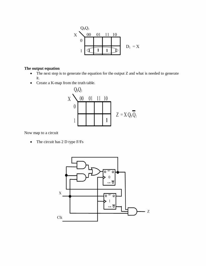
The output equation
The next step is to generate the equation for the output Z and what is needed to generate
it.
Create a K-map from the truth table.
Now map to a circuit
The circuit has 2 D type F/Fs
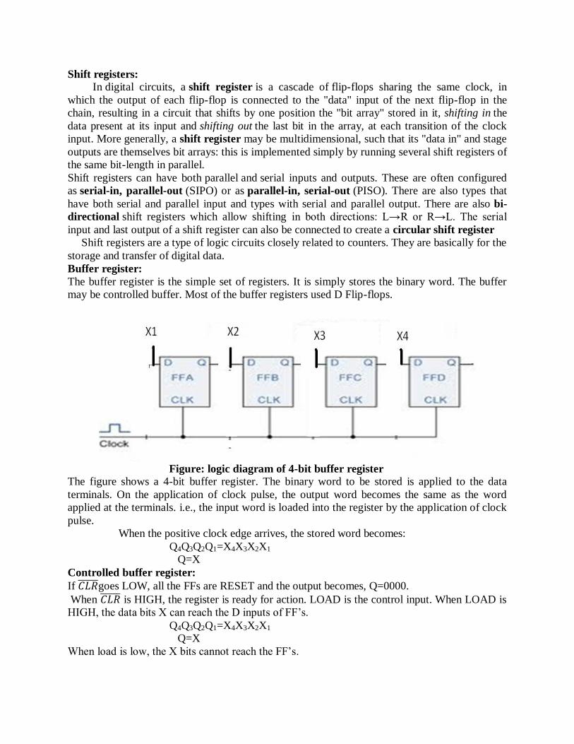
Shift registers:
In digital circuits, a shift register is a cascade of flip-flops sharing the same clock, in
which the output of each flip-flop is connected to the "data" input of the next flip-flop in the
chain, resulting in a circuit that shifts by one position the "bit array" stored in it, shifting in the
data present at its input and shifting out the last bit in the array, at each transition of the clock
input. More generally, a shift register may be multidimensional, such that its "data in" and stage
outputs are themselves bit arrays: this is implemented simply by running several shift registers of
the same bit-length in parallel.
Shift registers can have both parallel and serial inputs and outputs. These are often configured
as serial-in, parallel-out (SIPO) or as parallel-in, serial-out (PISO). There are also types that
have both serial and parallel input and types with serial and parallel output. There are also bi-
directional shift registers which allow shifting in both directions: L→R or R→L. The serial
input and last output of a shift register can also be connected to create a circular shift register
Shift registers are a type of logic circuits closely related to counters. They are basically for the
storage and transfer of digital data.
Buffer register:
The buffer register is the simple set of registers. It is simply stores the binary word. The buffer
may be controlled buffer. Most of the buffer registers used D Flip-flops.
Figure: logic diagram of 4-bit buffer register
The figure shows a 4-bit buffer register. The binary word to be stored is applied to the data
terminals. On the application of clock pulse, the output word becomes the same as the word
applied at the terminals. i.e., the input word is loaded into the register by the application of clock
pulse.
When the positive clock edge arrives, the stored word becomes:
Q4Q3Q2Q1=X4X3X2X1
Q=X
Controlled buffer register:
If 𝐶𝐿𝑅 goes LOW, all the FFs are RESET and the output becomes, Q=0000.
When 𝐶𝐿𝑅 is HIGH, the register is ready for action. LOAD is the control input. When LOAD is
HIGH, the data bits X can reach the D inputs of FF‘s.
Q4Q3Q2Q1=X4X3X2X1
Q=X
When load is low, the X bits cannot reach the FF‘s.
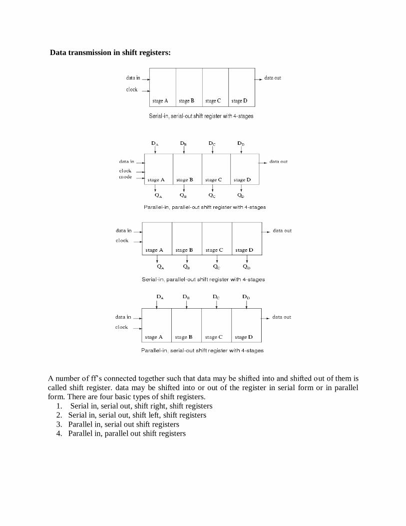
Data transmission in shift registers:
A number of ff‘s connected together such that data may be shifted into and shifted out of them is
called shift register. data may be shifted into or out of the register in serial form or in parallel
form. There are four basic types of shift registers.
1. Serial in, serial out, shift right, shift registers
2. Serial in, serial out, shift left, shift registers
3. Parallel in, serial out shift registers
4. Parallel in, parallel out shift registers
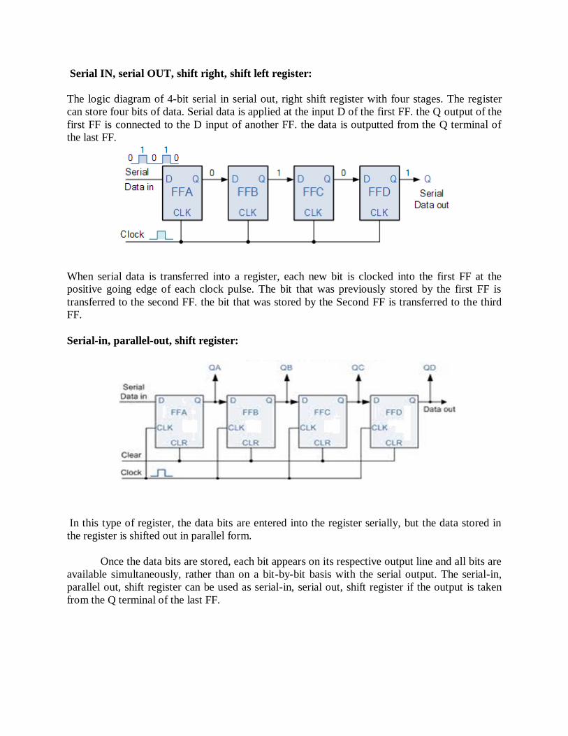
Serial IN, serial OUT, shift right, shift left register:
The logic diagram of 4-bit serial in serial out, right shift register with four stages. The register
can store four bits of data. Serial data is applied at the input D of the first FF. the Q output of the
first FF is connected to the D input of another FF. the data is outputted from the Q terminal of
the last FF.
When serial data is transferred into a register, each new bit is clocked into the first FF at the
positive going edge of each clock pulse. The bit that was previously stored by the first FF is
transferred to the second FF. the bit that was stored by the Second FF is transferred to the third
FF.
Serial-in, parallel-out, shift register:
In this type of register, the data bits are entered into the register serially, but the data stored in
the register is shifted out in parallel form.
Once the data bits are stored, each bit appears on its respective output line and all bits are
available simultaneously, rather than on a bit-by-bit basis with the serial output. The serial-in,
parallel out, shift register can be used as serial-in, serial out, shift register if the output is taken
from the Q terminal of the last FF.
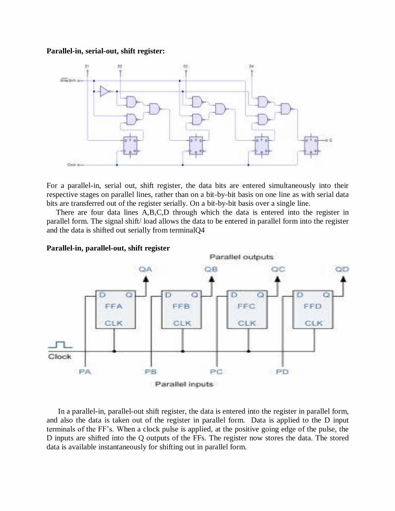
Parallel-in, serial-out, shift register:
For a parallel-in, serial out, shift register, the data bits are entered simultaneously into their
respective stages on parallel lines, rather than on a bit-by-bit basis on one line as with serial data
bits are transferred out of the register serially. On a bit-by-bit basis over a single line.
There are four data lines A,B,C,D through which the data is entered into the register in
parallel form. The signal shift/ load allows the data to be entered in parallel form into the register
and the data is shifted out serially from terminalQ4
Parallel-in, parallel-out, shift register
In a parallel-in, parallel-out shift register, the data is entered into the register in parallel form,
and also the data is taken out of the register in parallel form. Data is applied to the D input
terminals of the FF‘s. When a clock pulse is applied, at the positive going edge of the pulse, the
D inputs are shifted into the Q outputs of the FFs. The register now stores the data. The stored
data is available instantaneously for shifting out in parallel form.
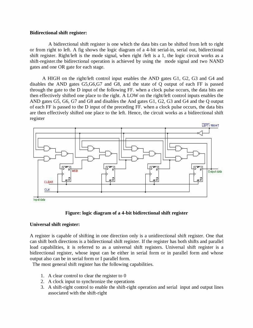
Bidirectional shift register:
A bidirectional shift register is one which the data bits can be shifted from left to right
or from right to left. A fig shows the logic diagram of a 4-bit serial-in, serial out, bidirectional
shift register. Right/left is the mode signal, when right /left is a 1, the logic circuit works as a
shift-register.the bidirectional operation is achieved by using the mode signal and two NAND
gates and one OR gate for each stage.
A HIGH on the right/left control input enables the AND gates G1, G2, G3 and G4 and
disables the AND gates G5,G6,G7 and G8, and the state of Q output of each FF is passed
through the gate to the D input of the following FF. when a clock pulse occurs, the data bits are
then effectively shifted one place to the right. A LOW on the right/left control inputs enables the
AND gates G5, G6, G7 and G8 and disables the And gates G1, G2, G3 and G4 and the Q output
of each FF is passed to the D input of the preceding FF. when a clock pulse occurs, the data bits
are then effectively shifted one place to the left. Hence, the circuit works as a bidirectional shift
register
Figure: logic diagram of a 4-bit bidirectional shift register
Universal shift register:
A register is capable of shifting in one direction only is a unidirectional shift register. One that
can shift both directions is a bidirectional shift register. If the register has both shifts and parallel
load capabilities, it is referred to as a universal shift registers. Universal shift register is a
bidirectional register, whose input can be either in serial form or in parallel form and whose
output also can be in serial form or I parallel form.
The most general shift register has the following capabilities.
1. A clear control to clear the register to 0
2. A clock input to synchronize the operations
3. A shift-right control to enable the shift-right operation and serial input and output lines
associated with the shift-right
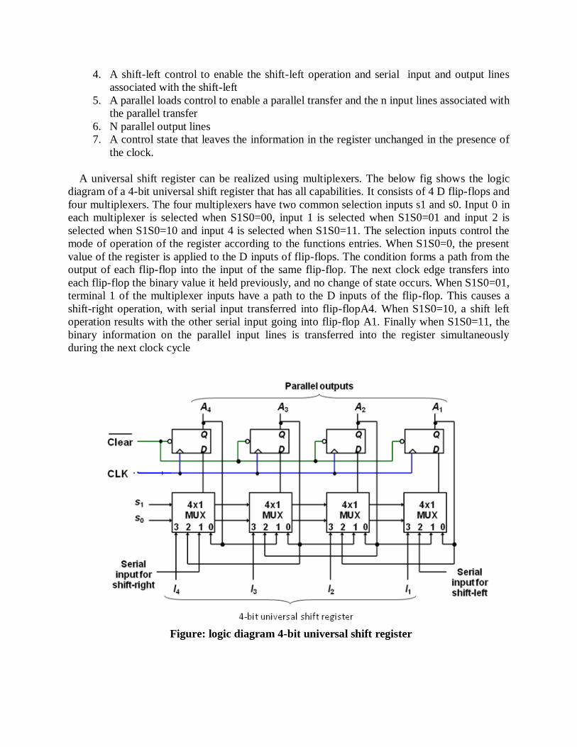
4. A shift-left control to enable the shift-left operation and serial input and output lines
associated with the shift-left
5. A parallel loads control to enable a parallel transfer and the n input lines associated with
the parallel transfer
6. N parallel output lines
7. A control state that leaves the information in the register unchanged in the presence of
the clock.
A universal shift register can be realized using multiplexers. The below fig shows the logic
diagram of a 4-bit universal shift register that has all capabilities. It consists of 4 D flip-flops and
four multiplexers. The four multiplexers have two common selection inputs s1 and s0. Input 0 in
each multiplexer is selected when S1S0=00, input 1 is selected when S1S0=01 and input 2 is
selected when S1S0=10 and input 4 is selected when S1S0=11. The selection inputs control the
mode of operation of the register according to the functions entries. When S1S0=0, the present
value of the register is applied to the D inputs of flip-flops. The condition forms a path from the
output of each flip-flop into the input of the same flip-flop. The next clock edge transfers into
each flip-flop the binary value it held previously, and no change of state occurs. When S1S0=01,
terminal 1 of the multiplexer inputs have a path to the D inputs of the flip-flop. This causes a
shift-right operation, with serial input transferred into flip-flopA4. When S1S0=10, a shift left
operation results with the other serial input going into flip-flop A1. Finally when S1S0=11, the
binary information on the parallel input lines is transferred into the register simultaneously
during the next clock cycle
Figure: logic diagram 4-bit universal shift register

Function table for theregister
mode control
S0 S1 register operation
0 0 No change
0 1 Shift Right
1 0 Shift left
1 1 Parallel load
Counters:
Counter is a device which stores (and sometimes displays) the number of times
particular event or process has occurred, often in relationship to a clock signal. A Digital counter
is a set of flip flops whose state change in response to pulses applied at the input to the counter.
Counters may be asynchronous counters or synchronous counters. Asynchronous counters are
also called ripple counters
In electronics counters can be implemented quite easily using register-type circuits such as
the flip-flops and a wide variety of classifications exist:
Asynchronous (ripple) counter – changing state bits are used as clocks to subsequent state
flip-flops
Synchronous counter – all state bits change under control of a single clock
Decade counter – counts through ten states per stage
Up/down counter – counts both up and down, under command of a control input
Ring counter – formed by a shift register with feedback connection in a ring
Johnson counter – a twisted ring counter
Cascaded counter
Modulus counter.
Each is useful for different applications. Usually, counter circuits are digital in nature, and count
in natural binary Many types of counter circuits are available as digital building blocks, for
example a number of chips in the 4000 series implement different counters.
Occasionally there are advantages to using a counting sequence other than the natural binary
sequence such as the binary coded decimal counter, a linear feed-back shift register counter, or
a gray-code counter.
Counters are useful for digital clocks and timers, and in oven timers, VCR clocks, etc.
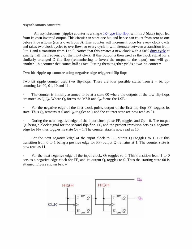
Asynchronous counters:
An asynchronous (ripple) counter is a single JK-type flip-flop, with its J (data) input fed
from its own inverted output. This circuit can store one bit, and hence can count from zero to one
before it overflows (starts over from 0). This counter will increment once for every clock cycle
and takes two clock cycles to overflow, so every cycle it will alternate between a transition from
0 to 1 and a transition from 1 to 0. Notice that this creates a new clock with a 50% duty cycle at
exactly half the frequency of the input clock. If this output is then used as the clock signal for a
similarly arranged D flip-flop (remembering to invert the output to the input), one will get
another 1 bit counter that counts half as fast. Putting them together yields a two-bit counter:
Two-bit ripple up-counter using negative edge triggered flip flop:
Two bit ripple counter used two flip-flops. There are four possible states from 2 – bit up-
counting I.e. 00, 01, 10 and 11.
· The counter is initially assumed to be at a state 00 where the outputs of the tow flip-flops
are noted as Q1Q0. Where Q1 forms the MSB and Q0 forms the LSB.
· For the negative edge of the first clock pulse, output of the first flip-flop FF1 toggles its
state. Thus Q1 remains at 0 and Q0 toggles to 1 and the counter state are now read as 01.
· During the next negative edge of the input clock pulse FF1 toggles and Q0 = 0. The output
Q0 being a clock signal for the second flip-flop FF2 and the present transition acts as a negative
edge for FF2 thus toggles its state Q1 = 1. The counter state is now read as 10.
· For the next negative edge of the input clock to FF1 output Q0 toggles to 1. But this
transition from 0 to 1 being a positive edge for FF2 output Q1 remains at 1. The counter state is
now read as 11.
· For the next negative edge of the input clock, Q0 toggles to 0. This transition from 1 to 0
acts as a negative edge clock for FF2 and its output Q1 toggles to 0. Thus the starting state 00 is
attained. Figure shown below
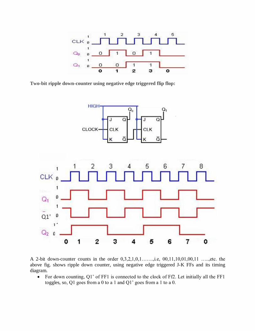
Two-bit ripple down-counter using negative edge triggered flip flop:
A 2-bit down-counter counts in the order 0,3,2,1,0,1…….,i.e, 00,11,10,01,00,11 …..,etc. the
above fig. shows ripple down counter, using negative edge triggered J-K FFs and its timing
diagram.
For down counting, Q1‘ of FF1 is connected to the clock of Ff2. Let initially all the FF1
toggles, so, Q1 goes from a 0 to a 1 and Q1‘ goes from a 1 to a 0.
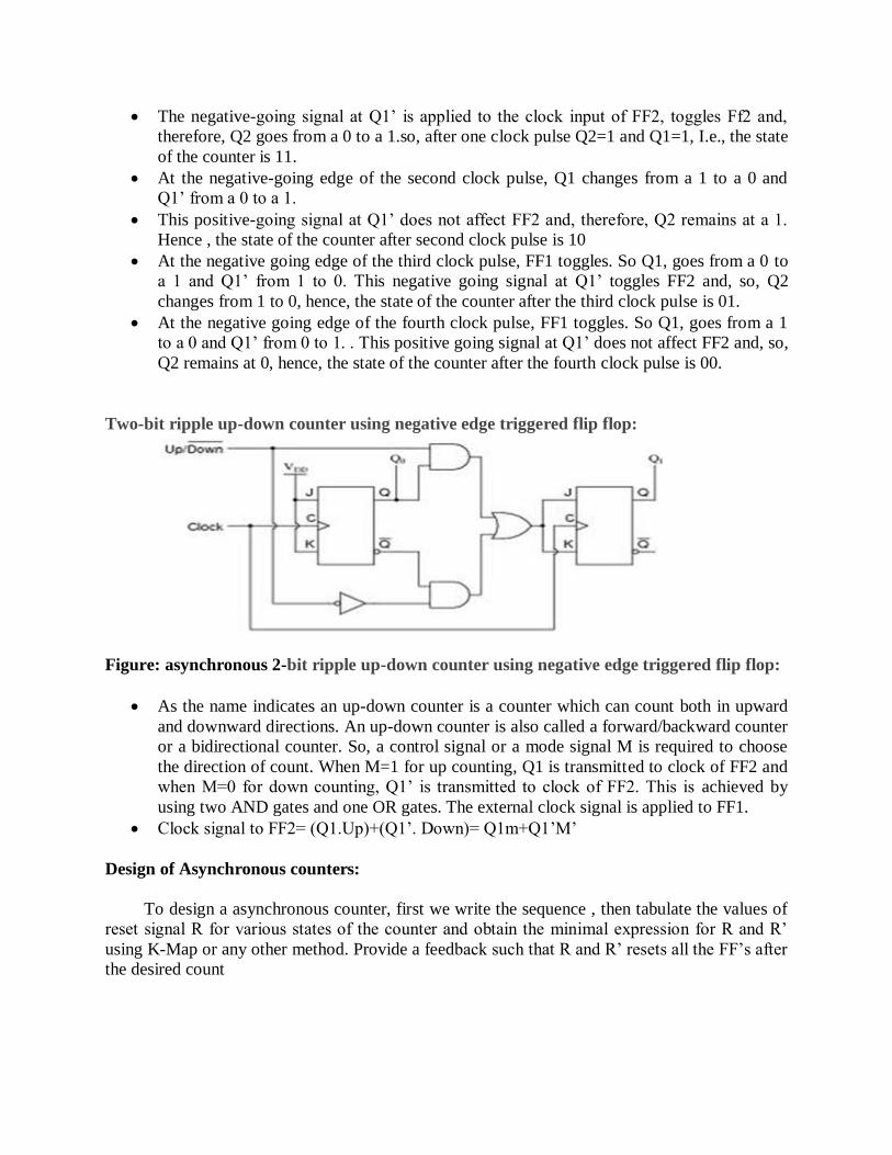
The negative-going signal at Q1‘ is applied to the clock input of FF2, toggles Ff2 and,
therefore, Q2 goes from a 0 to a 1.so, after one clock pulse Q2=1 and Q1=1, I.e., the state
of the counter is 11.
At the negative-going edge of the second clock pulse, Q1 changes from a 1 to a 0 and
Q1‘ from a 0 to a 1.
This positive-going signal at Q1‘ does not affect FF2 and, therefore, Q2 remains at a 1.
Hence , the state of the counter after second clock pulse is 10
At the negative going edge of the third clock pulse, FF1 toggles. So Q1, goes from a 0 to
a 1 and Q1‘ from 1 to 0. This negative going signal at Q1‘ toggles FF2 and, so, Q2
changes from 1 to 0, hence, the state of the counter after the third clock pulse is 01.
At the negative going edge of the fourth clock pulse, FF1 toggles. So Q1, goes from a 1
to a 0 and Q1‘ from 0 to 1. . This positive going signal at Q1‘ does not affect FF2 and, so,
Q2 remains at 0, hence, the state of the counter after the fourth clock pulse is 00.
Two-bit ripple up-down counter using negative edge triggered flip flop:
Figure: asynchronous 2-bit ripple up-down counter using negative edge triggered flip flop:
As the name indicates an up-down counter is a counter which can count both in upward
and downward directions. An up-down counter is also called a forward/backward counter
or a bidirectional counter. So, a control signal or a mode signal M is required to choose
the direction of count. When M=1 for up counting, Q1 is transmitted to clock of FF2 and
when M=0 for down counting, Q1‘ is transmitted to clock of FF2. This is achieved by
using two AND gates and one OR gates. The external clock signal is applied to FF1.
Clock signal to FF2= (Q1.Up)+(Q1‘. Down)= Q1m+Q1‘M‘
Design of Asynchronous counters:
To design a asynchronous counter, first we write the sequence , then tabulate the values of
reset signal R for various states of the counter and obtain the minimal expression for R and R‘
using K-Map or any other method. Provide a feedback such that R and R‘ resets all the FF‘s after
the desired count
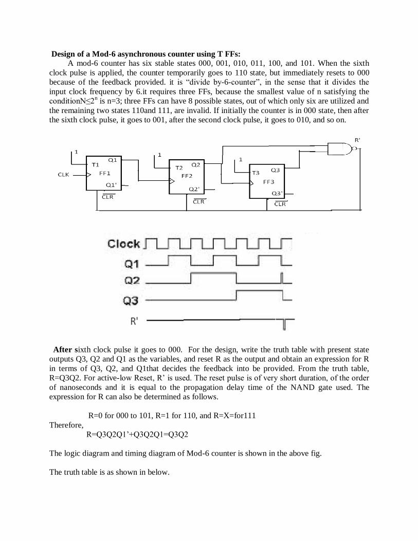
Design of a Mod-6 asynchronous counter using T FFs:
A mod-6 counter has six stable states 000, 001, 010, 011, 100, and 101. When the sixth
clock pulse is applied, the counter temporarily goes to 110 state, but immediately resets to 000
because of the feedback provided. it is ―divide by-6-counter‖, in the sense that it divides the
input clock frequency by 6.it requires three FFs, because the smallest value of n satisfying the
conditionN≤2n is n=3; three FFs can have 8 possible states, out of which only six are utilized and
the remaining two states 110and 111, are invalid. If initially the counter is in 000 state, then after
the sixth clock pulse, it goes to 001, after the second clock pulse, it goes to 010, and so on.
After sixth clock pulse it goes to 000. For the design, write the truth table with present state
outputs Q3, Q2 and Q1 as the variables, and reset R as the output and obtain an expression for R
in terms of Q3, Q2, and Q1that decides the feedback into be provided. From the truth table,
R=Q3Q2. For active-low Reset, R‘ is used. The reset pulse is of very short duration, of the order
of nanoseconds and it is equal to the propagation delay time of the NAND gate used. The
expression for R can also be determined as follows.
R=0 for 000 to 101, R=1 for 110, and R=X=for111
Therefore,
R=Q3Q2Q1‘+Q3Q2Q1=Q3Q2
The logic diagram and timing diagram of Mod-6 counter is shown in the above fig.
The truth table is as shown in below.
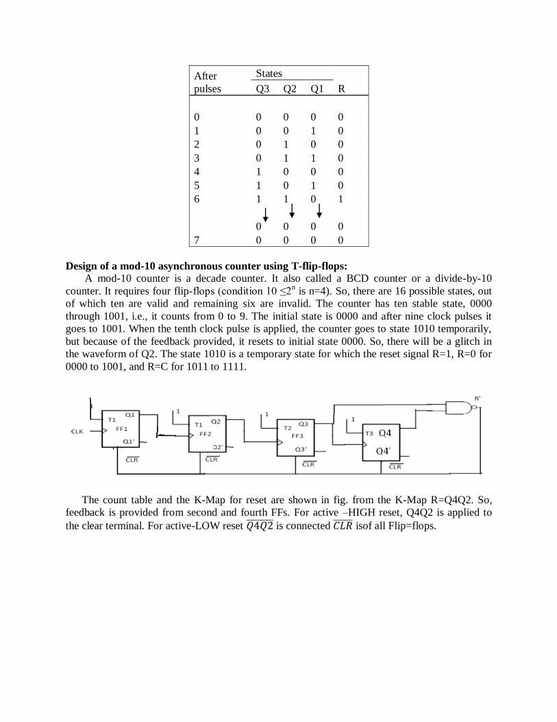
After
pulses
States
R Q3 Q2 Q1
0 0 0 0 0
1 0 0 1 0
2 0 1 0 0
3 0 1 1 0
4 1 0 0 0
5 1 0 1 0
6 1 1 0 1
0 0 0 0
7 0 0 0 0
Design of a mod-10 asynchronous counter using T-flip-flops:
A mod-10 counter is a decade counter. It also called a BCD counter or a divide-by-10
counter. It requires four flip-flops (condition 10 ≤2n is n=4). So, there are 16 possible states, out
of which ten are valid and remaining six are invalid. The counter has ten stable state, 0000
through 1001, i.e., it counts from 0 to 9. The initial state is 0000 and after nine clock pulses it
goes to 1001. When the tenth clock pulse is applied, the counter goes to state 1010 temporarily,
but because of the feedback provided, it resets to initial state 0000. So, there will be a glitch in
the waveform of Q2. The state 1010 is a temporary state for which the reset signal R=1, R=0 for
0000 to 1001, and R=C for 1011 to 1111.
The count table and the K-Map for reset are shown in fig. from the K-Map R=Q4Q2. So,
feedback is provided from second and fourth FFs. For active –HIGH reset, Q4Q2 is applied to
the clear terminal. For active-LOW reset 𝑄4𝑄2 is connected 𝐶𝐿𝑅 isof all Flip=flops.
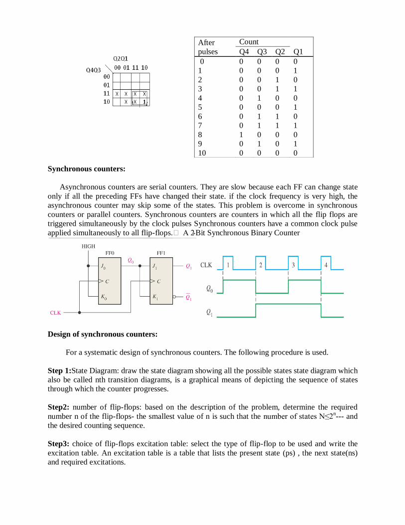
Synchronous counters:
Asynchronous counters are serial counters. They are slow because each FF can change state
only if all the preceding FFs have changed their state. if the clock frequency is very high, the
asynchronous counter may skip some of the states. This problem is overcome in synchronous
counters or parallel counters. Synchronous counters are counters in which all the flip flops are
triggered simultaneously by the clock pulses Synchronous counters have a common clock pulse
applied simultaneously to all flip-flops. A 2-Bit Synchronous Binary Counter
Design of synchronous counters:
For a systematic design of synchronous counters. The following procedure is used.
Step 1:State Diagram: draw the state diagram showing all the possible states state diagram which
also be called nth transition diagrams, is a graphical means of depicting the sequence of states
through which the counter progresses.
Step2: number of flip-flops: based on the description of the problem, determine the required
number n of the flip-flops- the smallest value of n is such that the number of states N≤2n--- and
the desired counting sequence.
Step3: choice of flip-flops excitation table: select the type of flip-flop to be used and write the
excitation table. An excitation table is a table that lists the present state (ps) , the next state(ns)
and required excitations.
After
pulses
Count
Q1 Q4 Q3 Q2
0 0 0 0 0
1 0 0 0 1
2 0 0 1 0
3 0 0 1 1
4 0 1 0 0
5 0 0 0 1
6 0 1 1 0
7 0 1 1 1
8 1 0 0 0
9 0 1 0 1
10 0 0 0 0
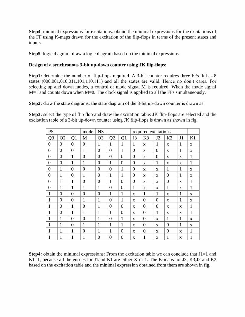
Step4: minimal expressions for excitations: obtain the minimal expressions for the excitations of
the FF using K-maps drawn for the excitation of the flip-flops in terms of the present states and
inputs.
Step5: logic diagram: draw a logic diagram based on the minimal expressions
Design of a synchronous 3-bit up-down counter using JK flip-flops:
Step1: determine the number of flip-flops required. A 3-bit counter requires three FFs. It has 8
states (000,001,010,011,101,110,111) and all the states are valid. Hence no don‘t cares. For
selecting up and down modes, a control or mode signal M is required. When the mode signal
M=1 and counts down when M=0. The clock signal is applied to all the FFs simultaneously.
Step2: draw the state diagrams: the state diagram of the 3-bit up-down counter is drawn as
Step3: select the type of flip flop and draw the excitation table: JK flip-flops are selected and the
excitation table of a 3-bit up-down counter using JK flip-flops is drawn as shown in fig.
PS mode NS required excitations
Q3 Q2 Q1 M Q3 Q2 Q1 J3 K3 J2 K2 J1 K1
0 0 0 0 1 1 1 1 x 1 x 1 x
0 0 0 1 0 0 1 0 x 0 x 1 x
0 0 1 0 0 0 0 0 x 0 x x 1
0 0 1 1 0 1 0 0 x 1 x x 1
0 1 0 0 0 0 1 0 x x 1 1 x
0 1 0 1 0 1 1 0 x x 0 1 x
0 1 1 0 0 1 0 0 x x 0 x 1
0 1 1 1 1 0 0 1 x x 1 x 1
1 0 0 0 0 1 1 x 1 1 x 1 x
1 0 0 1 1 0 1 x 0 0 x 1 x
1 0 1 0 1 0 0 x 0 0 x x 1
1 0 1 1 1 1 0 x 0 1 x x 1
1 1 0 0 1 0 1 x 0 x 1 1 x
1 1 0 1 1 1 1 x 0 x 0 1 x
1 1 1 0 1 1 0 x 0 x 0 x 1
1 1 1 1 0 0 0 x 1 x 1 x 1
Step4: obtain the minimal expressions: From the excitation table we can conclude that J1=1 and
K1=1, because all the entries for J1and K1 are either X or 1. The K-maps for J3, K3,J2 and K2
based on the excitation table and the minimal expression obtained from them are shown in fig.
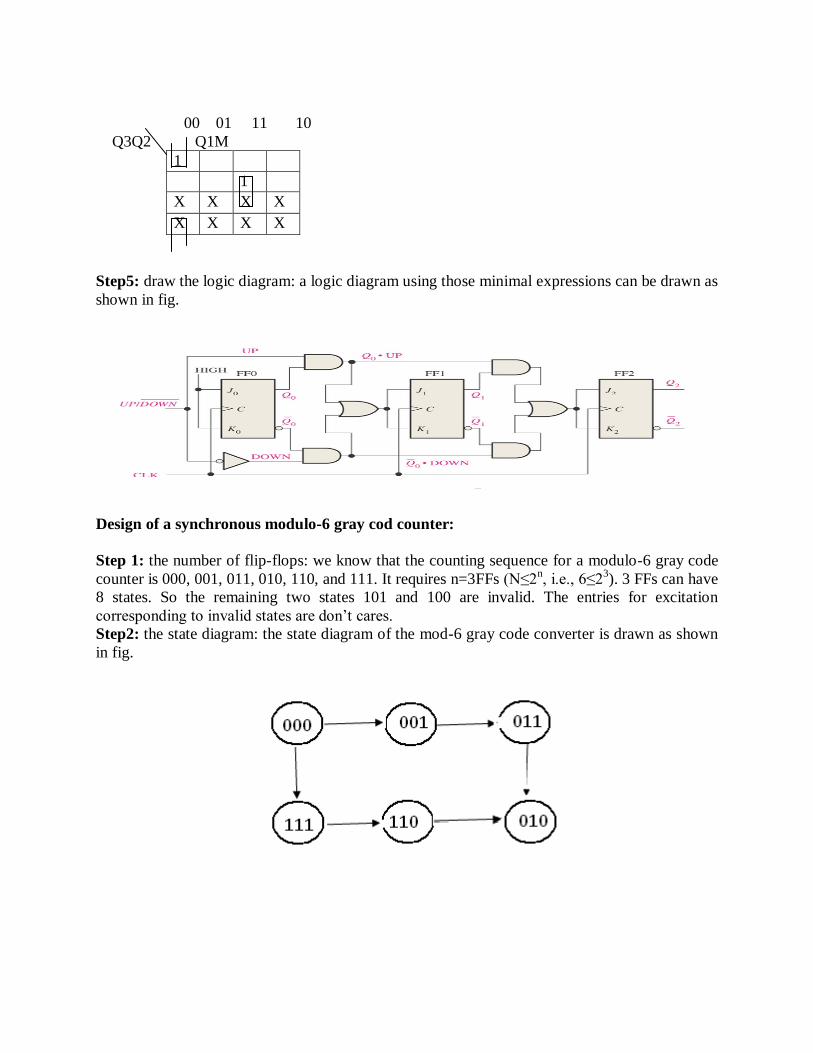
00 01 11 10
Q3Q2 Q1M
1
1
X X X X
X X X X
Step5: draw the logic diagram: a logic diagram using those minimal expressions can be drawn as
shown in fig.
Design of a synchronous modulo-6 gray cod counter:
Step 1: the number of flip-flops: we know that the counting sequence for a modulo-6 gray code
counter is 000, 001, 011, 010, 110, and 111. It requires n=3FFs (N≤2n, i.e., 6≤2
3). 3 FFs can have
8 states. So the remaining two states 101 and 100 are invalid. The entries for excitation
corresponding to invalid states are don‘t cares.
Step2: the state diagram: the state diagram of the mod-6 gray code converter is drawn as shown
in fig.
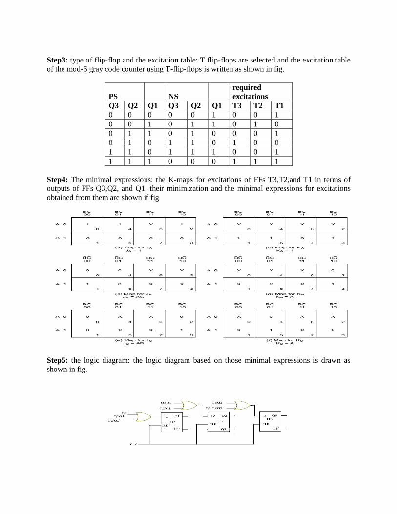
Step3: type of flip-flop and the excitation table: T flip-flops are selected and the excitation table
of the mod-6 gray code counter using T-flip-flops is written as shown in fig.
PS NS
required
excitations
Q3 Q2 Q1 Q3 Q2 Q1 T3 T2 T1
0 0 0 0 0 1 0 0 1
0 0 1 0 1 1 0 1 0
0 1 1 0 1 0 0 0 1
0 1 0 1 1 0 1 0 0
1 1 0 1 1 1 0 0 1
1 1 1 0 0 0 1 1 1
Step4: The minimal expressions: the K-maps for excitations of FFs T3,T2,and T1 in terms of
outputs of FFs Q3,Q2, and Q1, their minimization and the minimal expressions for excitations
obtained from them are shown if fig
Step5: the logic diagram: the logic diagram based on those minimal expressions is drawn as
shown in fig.
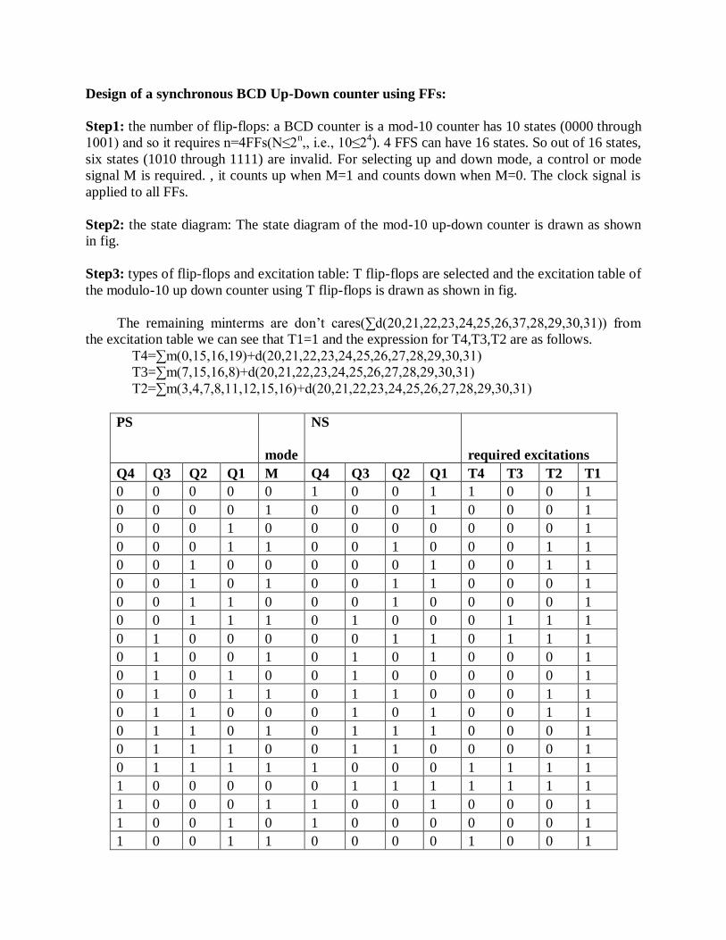
Design of a synchronous BCD Up-Down counter using FFs:
Step1: the number of flip-flops: a BCD counter is a mod-10 counter has 10 states (0000 through
1001) and so it requires n=4FFs(N≤2n,, i.e., 10≤2
4). 4 FFS can have 16 states. So out of 16 states,
six states (1010 through 1111) are invalid. For selecting up and down mode, a control or mode
signal M is required. , it counts up when M=1 and counts down when M=0. The clock signal is
applied to all FFs.
Step2: the state diagram: The state diagram of the mod-10 up-down counter is drawn as shown
in fig.
Step3: types of flip-flops and excitation table: T flip-flops are selected and the excitation table of
the modulo-10 up down counter using T flip-flops is drawn as shown in fig.
The remaining minterms are don‘t cares(∑d(20,21,22,23,24,25,26,37,28,29,30,31)) from
the excitation table we can see that T1=1 and the expression for T4,T3,T2 are as follows.
T4=∑m(0,15,16,19)+d(20,21,22,23,24,25,26,27,28,29,30,31)
T3=∑m(7,15,16,8)+d(20,21,22,23,24,25,26,27,28,29,30,31)
T2=∑m(3,4,7,8,11,12,15,16)+d(20,21,22,23,24,25,26,27,28,29,30,31)
PS
mode
NS
required excitations
Q4 Q3 Q2 Q1 M Q4 Q3 Q2 Q1 T4 T3 T2 T1
0 0 0 0 0 1 0 0 1 1 0 0 1
0 0 0 0 1 0 0 0 1 0 0 0 1
0 0 0 1 0 0 0 0 0 0 0 0 1
0 0 0 1 1 0 0 1 0 0 0 1 1
0 0 1 0 0 0 0 0 1 0 0 1 1
0 0 1 0 1 0 0 1 1 0 0 0 1
0 0 1 1 0 0 0 1 0 0 0 0 1
0 0 1 1 1 0 1 0 0 0 1 1 1
0 1 0 0 0 0 0 1 1 0 1 1 1
0 1 0 0 1 0 1 0 1 0 0 0 1
0 1 0 1 0 0 1 0 0 0 0 0 1
0 1 0 1 1 0 1 1 0 0 0 1 1
0 1 1 0 0 0 1 0 1 0 0 1 1
0 1 1 0 1 0 1 1 1 0 0 0 1
0 1 1 1 0 0 1 1 0 0 0 0 1
0 1 1 1 1 1 0 0 0 1 1 1 1
1 0 0 0 0 0 1 1 1 1 1 1 1
1 0 0 0 1 1 0 0 1 0 0 0 1
1 0 0 1 0 1 0 0 0 0 0 0 1
1 0 0 1 1 0 0 0 0 1 0 0 1
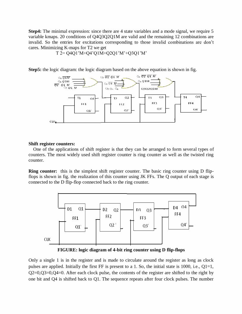
Step4: The minimal expression: since there are 4 state variables and a mode signal, we require 5
variable kmaps. 20 conditions of Q4Q3Q2Q1M are valid and the remaining 12 combinations are
invalid. So the entries for excitations corresponding to those invalid combinations are don‘t
cares. Minimizing K-maps for T2 we get
T 2= Q4Q1‘M+Q4‘Q1M+Q2Q1‘M‘+Q3Q1‘M‘
Step5: the logic diagram: the logic diagram based on the above equation is shown in fig.
Shift register counters:
One of the applications of shift register is that they can be arranged to form several types of
counters. The most widely used shift register counter is ring counter as well as the twisted ring
counter.
Ring counter: this is the simplest shift register counter. The basic ring counter using D flip-
flops is shown in fig. the realization of this counter using JK FFs. The Q output of each stage is
connected to the D flip-flop connected back to the ring counter.
FIGURE: logic diagram of 4-bit ring counter using D flip-flops
Only a single 1 is in the register and is made to circulate around the register as long as clock
pulses are applied. Initially the first FF is present to a 1. So, the initial state is 1000, i.e., Q1=1,
Q2=0,Q3=0,Q4=0. After each clock pulse, the contents of the register are shifted to the right by
one bit and Q4 is shifted back to Q1. The sequence repeats after four clock pulses. The number
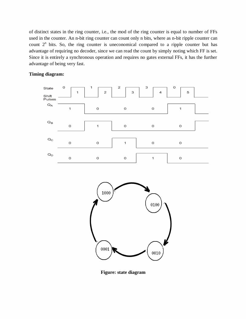
of distinct states in the ring counter, i.e., the mod of the ring counter is equal to number of FFs
used in the counter. An n-bit ring counter can count only n bits, where as n-bit ripple counter can
count 2n bits. So, the ring counter is uneconomical compared to a ripple counter but has
advantage of requiring no decoder, since we can read the count by simply noting which FF is set.
Since it is entirely a synchronous operation and requires no gates external FFs, it has the further
advantage of being very fast.
Timing diagram:
Figure: state diagram
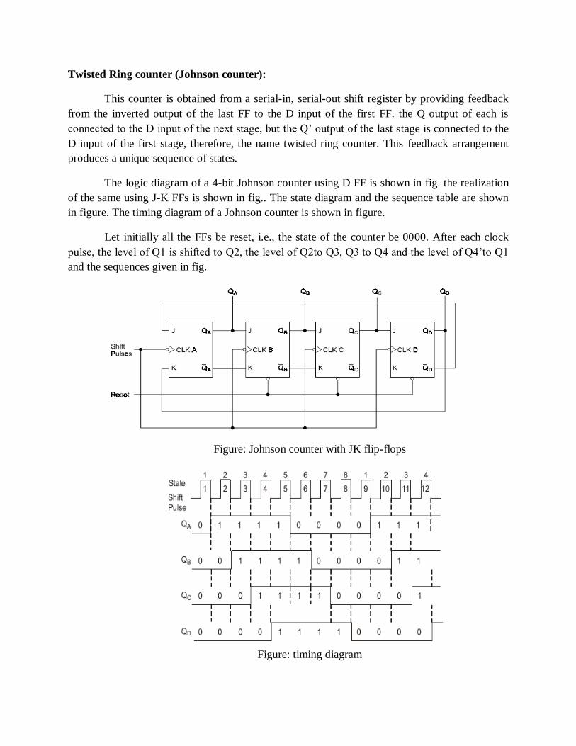
Twisted Ring counter (Johnson counter):
This counter is obtained from a serial-in, serial-out shift register by providing feedback
from the inverted output of the last FF to the D input of the first FF. the Q output of each is
connected to the D input of the next stage, but the Q‘ output of the last stage is connected to the
D input of the first stage, therefore, the name twisted ring counter. This feedback arrangement
produces a unique sequence of states.
The logic diagram of a 4-bit Johnson counter using D FF is shown in fig. the realization
of the same using J-K FFs is shown in fig.. The state diagram and the sequence table are shown
in figure. The timing diagram of a Johnson counter is shown in figure.
Let initially all the FFs be reset, i.e., the state of the counter be 0000. After each clock
pulse, the level of Q1 is shifted to Q2, the level of Q2to Q3, Q3 to Q4 and the level of Q4‘to Q1
and the sequences given in fig.
Figure: Johnson counter with JK flip-flops
Figure: timing diagram
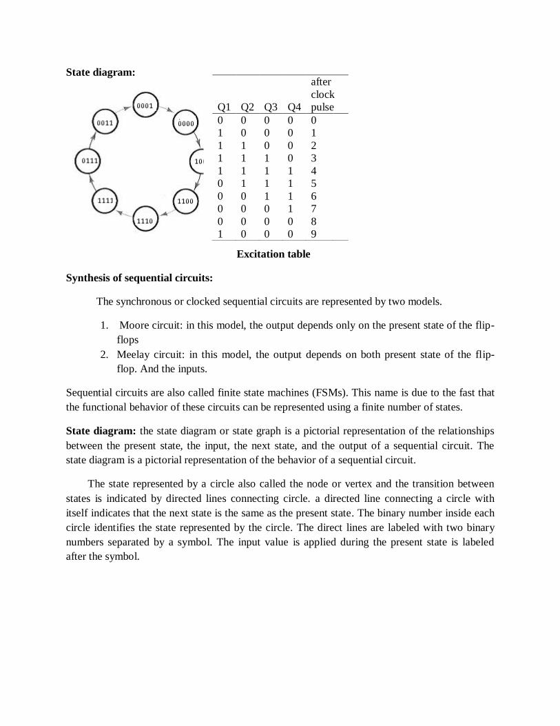
State diagram:
Excitation table
Synthesis of sequential circuits:
The synchronous or clocked sequential circuits are represented by two models.
1. Moore circuit: in this model, the output depends only on the present state of the flip-
flops
2. Meelay circuit: in this model, the output depends on both present state of the flip-
flop. And the inputs.
Sequential circuits are also called finite state machines (FSMs). This name is due to the fast that
the functional behavior of these circuits can be represented using a finite number of states.
State diagram: the state diagram or state graph is a pictorial representation of the relationships
between the present state, the input, the next state, and the output of a sequential circuit. The
state diagram is a pictorial representation of the behavior of a sequential circuit.
The state represented by a circle also called the node or vertex and the transition between
states is indicated by directed lines connecting circle. a directed line connecting a circle with
itself indicates that the next state is the same as the present state. The binary number inside each
circle identifies the state represented by the circle. The direct lines are labeled with two binary
numbers separated by a symbol. The input value is applied during the present state is labeled
after the symbol.
Q1 Q2 Q3 Q4
after
clock
pulse
0 0 0 0 0
1 0 0 0 1
1 1 0 0 2
1 1 1 0 3
1 1 1 1 4
0 1 1 1 5
0 0 1 1 6
0 0 0 1 7
0 0 0 0 8
1 0 0 0 9
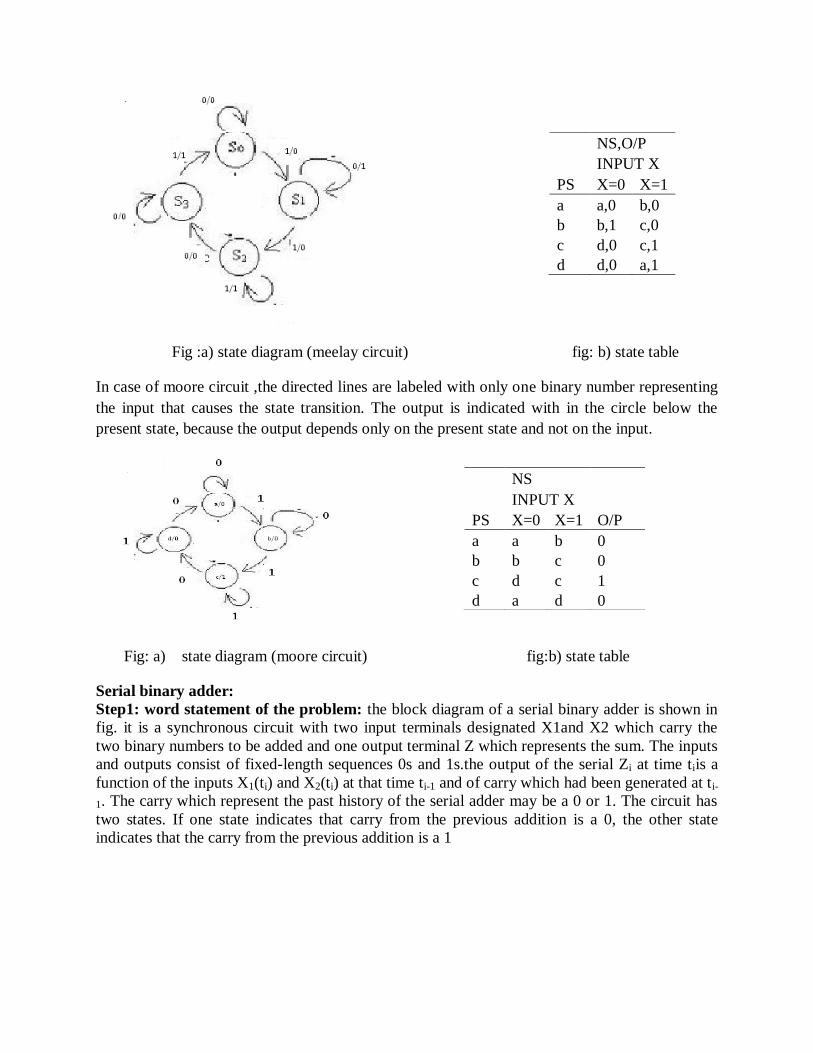
Fig :a) state diagram (meelay circuit) fig: b) state table
In case of moore circuit ,the directed lines are labeled with only one binary number representing
the input that causes the state transition. The output is indicated with in the circle below the
present state, because the output depends only on the present state and not on the input.
Fig: a) state diagram (moore circuit) fig:b) state table
Serial binary adder:
Step1: word statement of the problem: the block diagram of a serial binary adder is shown in
fig. it is a synchronous circuit with two input terminals designated X1and X2 which carry the
two binary numbers to be added and one output terminal Z which represents the sum. The inputs
and outputs consist of fixed-length sequences 0s and 1s.the output of the serial Zi at time tiis a
function of the inputs X1(ti) and X2(ti) at that time ti-1 and of carry which had been generated at ti-
1. The carry which represent the past history of the serial adder may be a 0 or 1. The circuit has
two states. If one state indicates that carry from the previous addition is a 0, the other state
indicates that the carry from the previous addition is a 1
PS
NS,O/P
INPUT X
X=0 X=1
a a,0 b,0
b b,1 c,0
c d,0 c,1
d d,0 a,1
PS
NS
O/P
INPUT X
X=0 X=1
a a b 0
b b c 0
c d c 1
d a d 0
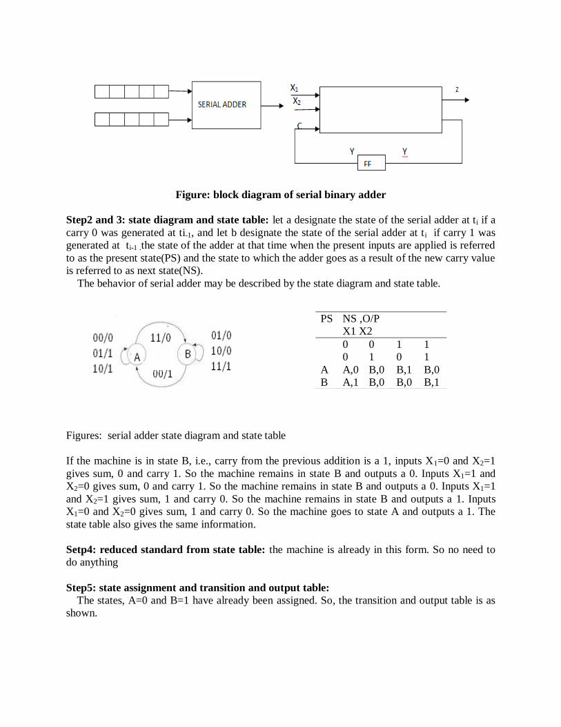
Figure: block diagram of serial binary adder
Step2 and 3: state diagram and state table: let a designate the state of the serial adder at ti if a
carry 0 was generated at ti-1, and let b designate the state of the serial adder at t i if carry 1 was
generated at ti-1 .the state of the adder at that time when the present inputs are applied is referred
to as the present state(PS) and the state to which the adder goes as a result of the new carry value
is referred to as next state(NS).
The behavior of serial adder may be described by the state diagram and state table.
Figures: serial adder state diagram and state table
If the machine is in state B, i.e., carry from the previous addition is a 1, inputs X1=0 and X2=1
gives sum, 0 and carry 1. So the machine remains in state B and outputs a 0. Inputs X1=1 and
X2=0 gives sum, 0 and carry 1. So the machine remains in state B and outputs a 0. Inputs X1=1
and X2=1 gives sum, 1 and carry 0. So the machine remains in state B and outputs a 1. Inputs
X1=0 and X2=0 gives sum, 1 and carry 0. So the machine goes to state A and outputs a 1. The
state table also gives the same information.
Setp4: reduced standard from state table: the machine is already in this form. So no need to
do anything
Step5: state assignment and transition and output table:
The states, A=0 and B=1 have already been assigned. So, the transition and output table is as
shown.
PS NS ,O/P
X1 X2
0
0
0
1
1
0
1
1
A A,0 B,0 B,1 B,0
B A,1 B,0 B,0 B,1
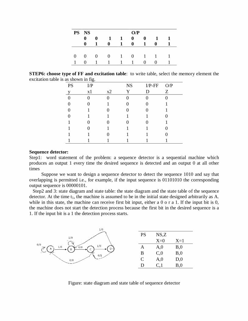
PS NS O/P
0
0
0
1
1
0
1
1
0
0
0
1
1
0
1
1
0 0 0 0 1 0 1 1 1
1 0 1 1 1 1 0 0 1
STEP6: choose type of FF and excitation table: to write table, select the memory element the
excitation table is as shown in fig.
PS I/P NS I/P-FF O/P
y x1 x2 Y D Z
0 0 0 0 0 0
0 0 1 0 0 1
0 1 0 0 0 1
0 1 1 1 1 0
1 0 0 0 0 1
1 0 1 1 1 0
1 1 0 1 1 0
1 1 1 1 1 1
Sequence detector:
Step1: word statement of the problem: a sequence detector is a sequential machine which
produces an output 1 every time the desired sequence is detected and an output 0 at all other
times
Suppose we want to design a sequence detector to detect the sequence 1010 and say that
overlapping is permitted i.e., for example, if the input sequence is 01101010 the corresponding
output sequence is 00000101.
Step2 and 3: state diagram and state table: the state diagram and the state table of the sequence
detector. At the time t1, the machine is assumed to be in the initial state designed arbitrarily as A.
while in this state, the machine can receive first bit input, either a 0 o r a 1. If the input bit is 0,
the machine does not start the detection process because the first bit in the desired sequence is a
1. If the input bit is a 1 the detection process starts.
Figure: state diagram and state table of sequence detector
PS NS,Z
X=0 X=1
A A,0 B,0
B C,0 B,0
C A,0 D,0
D C,1 B,0
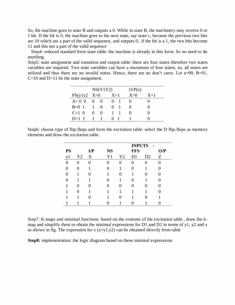
So, the machine goes to state B and outputs a 0. While in state B, the machinery may receive 0 or
1 bit. If the bit is 0, the machine goes to the next state, say state c, because the previous two bits
are 10 which are a part of the valid sequence, and outputs 0.. if the bit is a 1, the two bits become
11 and this not a part of the valid sequence
Step4: reduced standard form state table: the machine is already in this form. So no need to do
anything.
Step5: state assignment and transition and output table: there are four states therefore two states
variables are required. Two state variables can have a maximum of four states, so, all states are
utilized and thus there are no invalid states. Hence, there are no don‘t cares. Let a=00, B=01,
C=10 and D=11 be the state assignment.
NS(Y1Y2) O/P(z)
PS(y1y2 X=0 X=1 X=0 X=1
A= 0 0 0 0 0 1 0 0
B=0 1 1 0 0 1 0 0
C=1 0 0 0 1 1 0 0
D=1 1 1 1 0 1 1 0
Step6: choose type of flip-flops and form the excitation table: select the D flip-flops as memory
elements and draw the excitation table.
PS I/P NS
INPUTS -
FFS O/P
y1 Y2 X Y1 Y2 D1 D2 Z
0 0 0 0 0 0 0 0
0 0 1 0 1 0 1 0
0 1 0 1 0 1 0 0
0 1 1 0 1 0 1 0
1 0 0 0 0 0 0 0
1 0 1 1 1 1 1 0
1 1 0 1 0 1 0 1
1 1 1 0 1 0 1 0
Step7: K-maps and minimal functions: based on the contents of the excitation table , draw the k-
map and simplify them to obtain the minimal expressions for D1 and D2 in terms of y1, y2 and x
as shown in fig. The expression for z (z=y1,y2) can be obtained directly from table
Step8: implementation: the logic diagram based on these minimal expressions
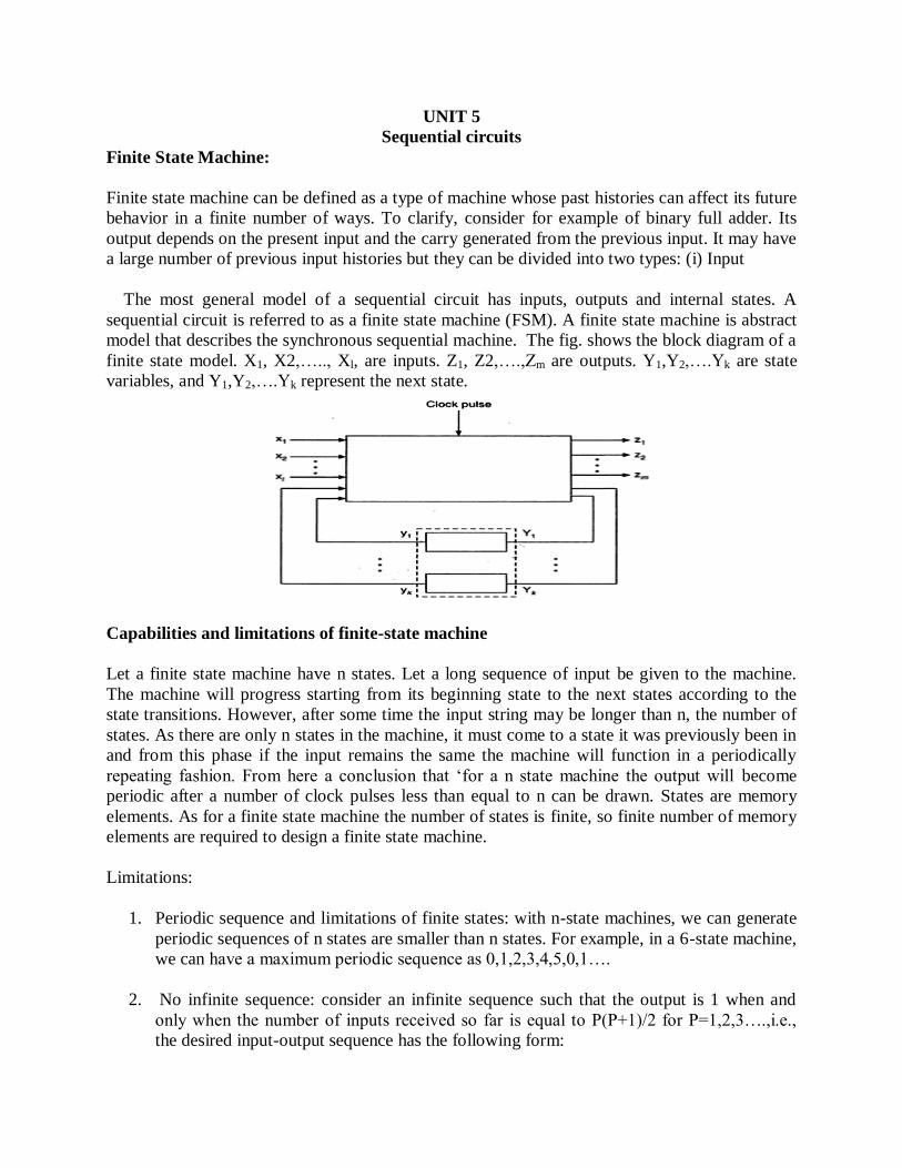
UNIT 5
Sequential circuits
Finite State Machine:
Finite state machine can be defined as a type of machine whose past histories can affect its future
behavior in a finite number of ways. To clarify, consider for example of binary full adder. Its
output depends on the present input and the carry generated from the previous input. It may have
a large number of previous input histories but they can be divided into two types: (i) Input
The most general model of a sequential circuit has inputs, outputs and internal states. A
sequential circuit is referred to as a finite state machine (FSM). A finite state machine is abstract
model that describes the synchronous sequential machine. The fig. shows the block diagram of a
finite state model. X1, X2,….., Xl, are inputs. Z1, Z2,….,Zm are outputs. Y1,Y2,….Yk are state
variables, and Y1,Y2,….Yk represent the next state.
Capabilities and limitations of finite-state machine
Let a finite state machine have n states. Let a long sequence of input be given to the machine.
The machine will progress starting from its beginning state to the next states according to the
state transitions. However, after some time the input string may be longer than n, the number of
states. As there are only n states in the machine, it must come to a state it was previously been in
and from this phase if the input remains the same the machine will function in a periodically
repeating fashion. From here a conclusion that ‗for a n state machine the output will become
periodic after a number of clock pulses less than equal to n can be drawn. States are memory
elements. As for a finite state machine the number of states is finite, so finite number of memory
elements are required to design a finite state machine.
Limitations:
1. Periodic sequence and limitations of finite states: with n-state machines, we can generate
periodic sequences of n states are smaller than n states. For example, in a 6-state machine,
we can have a maximum periodic sequence as 0,1,2,3,4,5,0,1….
2. No infinite sequence: consider an infinite sequence such that the output is 1 when and
only when the number of inputs received so far is equal to P(P+1)/2 for P=1,2,3….,i.e.,
the desired input-output sequence has the following form:
Input: x x x x x x x x x x x x x x x x x x x x x x
Output: 1 0 1 0 0 1 0 0 0 0 1 0 0 0 0 1 0 0 0 0 0 1
Such an infinite sequence cannot be produced by a finite state machine.
3. Limited memory: the finite state machine has a limited memory and due to limited
memory it cannot produce certain outputs. Consider a binary multiplier circuit for
multiplying two arbitrarily large binary numbers. The memory is not sufficient to store
arbitrarily large partial products resulted during multiplication.
Finite state machines are two types. They differ in the way the output is generate they are:
1. Mealy type model: in this model, the output is a function of the present state and the
present input.
2. Moore type model: in this model, the output is a function of the present state only.
Mathematical representation of synchronous sequential machine:
The relation between the present state S(t), present input X(t), and next state s(t+1) can be
given as
S(t+1)= f{S(t),X(t)}
The value of output Z(t) can be given as
Z(t)= g{S(t),X(t)} for mealy model
Z(t)= G{S(t)} for Moore model
Because, in a mealy machine, the output depends on the present state and input, where as in a
Moore machine, the output depends only on the present state.
Comparison between the Moore machine and mealy machine:
Moore machine mealy machine
1. its output is a function of present
state only Z(t)= g{S(t)}
1. its output is a function of present state
as well as present input Z(t)=g{S(t),X(t)}
2. input changes do not affect the
output
2. input changes may affect the output of
the circuit
3. it requires more number of states
for implementing same function
3. it requires less number of states for
implementing same function
Mealy model:
When the output of the sequential circuit depends on the both the present state of the flip-flops
and on the inputs, the sequential circuit is referred to as mealy circuit or mealy machine.
The fig. shows the logic diagram of the mealy model. Notice that the output depends up on the
present state as well as the present inputs. We can easily realize that changes in the input during
the clock pulse cannot affect the state of the flip-flop. They can affect the output of the circuit. If
the input variations are not synchronized with a clock, he derived output will also not be
synchronized with the clock and we get false output. The false outputs can be eliminated by
allowing input to change only at the active transition of the clock.
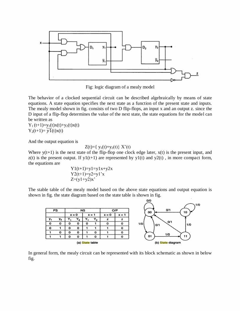
Fig: logic diagram of a mealy model
The behavior of a clocked sequential circuit can be described algebraically by means of state
equations. A state equation specifies the next state as a function of the present state and inputs.
The mealy model shown in fig. consists of two D flip-flops, an input x and an output z. since the
D input of a flip-flop determines the value of the next state, the state equations for the model can
be written as
Y1 (t+1)=y1(t)x(t)+y2(t)x(t)
Y2(t+1)= 𝑦1 (t)x(t)
And the output equation is
Z(t)={ y1(t)+y2(t)} X‘(t)
Where y(t+1) is the next state of the flip-flop one clock edge later, x(t) is the present input, and
z(t) is the present output. If y1(t+1) are represented by y1(t) and y2(t) , in more compact form,
the equations are
Y1(t+1)=y1=y1x+y2x
Y2(t+1)=y2=y1‘x Z=(y1+y2)x‘
The stable table of the mealy model based on the above state equations and output equation is
shown in fig. the state diagram based on the state table is shown in fig.
In general form, the mealy circuit can be represented with its block schematic as shown in below
fig.
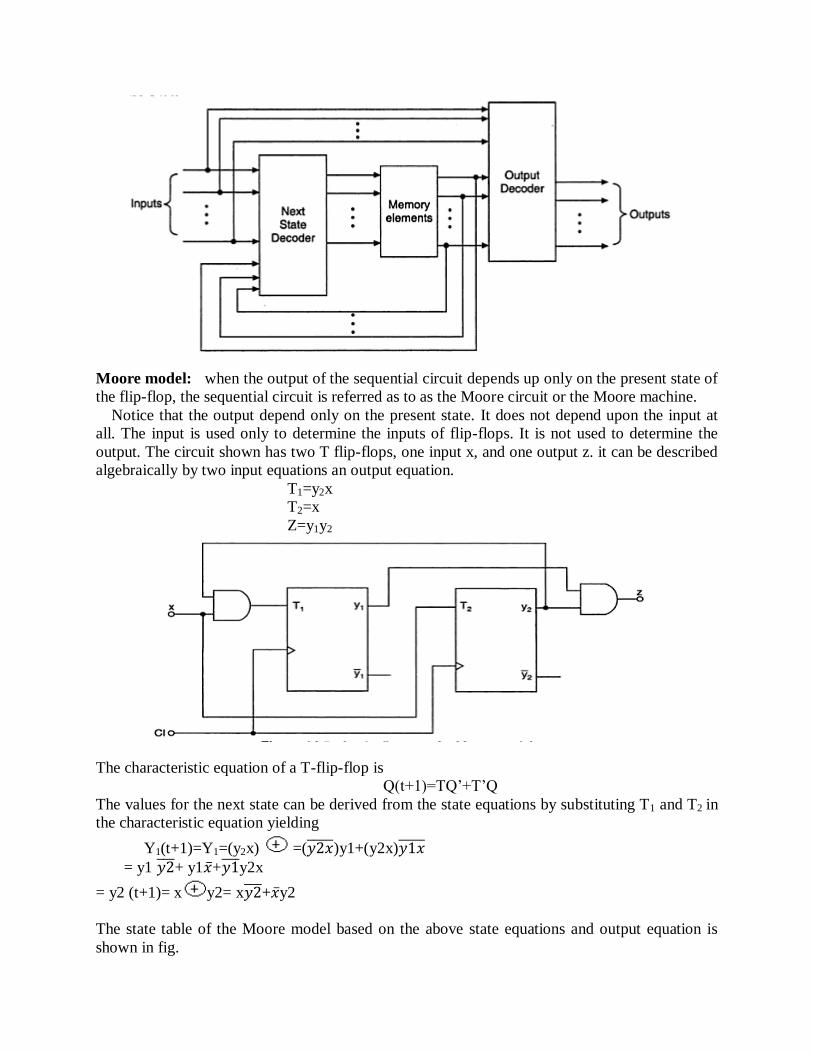
Moore model: when the output of the sequential circuit depends up only on the present state of
the flip-flop, the sequential circuit is referred as to as the Moore circuit or the Moore machine.
Notice that the output depend only on the present state. It does not depend upon the input at
all. The input is used only to determine the inputs of flip-flops. It is not used to determine the
output. The circuit shown has two T flip-flops, one input x, and one output z. it can be described
algebraically by two input equations an output equation.
T1=y2x
T2=x
Z=y1y2
The characteristic equation of a T-flip-flop is
Q(t+1)=TQ‘+T‘Q
The values for the next state can be derived from the state equations by substituting T1 and T2 in
the characteristic equation yielding
Y1(t+1)=Y1=(y2x) =(𝑦2𝑥 )y1+(y2x)𝑦1𝑥
= y1 𝑦2 + y1𝑥 +𝑦1 y2x
= y2 (t+1)= x y2= x𝑦2 +𝑥 y2
The state table of the Moore model based on the above state equations and output equation is
shown in fig.
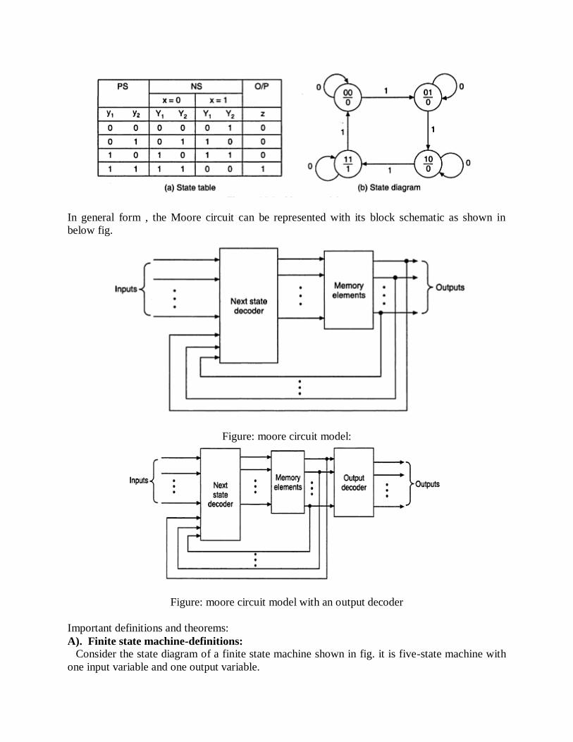
In general form , the Moore circuit can be represented with its block schematic as shown in
below fig.
Figure: moore circuit model:
Figure: moore circuit model with an output decoder
Important definitions and theorems:
A). Finite state machine-definitions:
Consider the state diagram of a finite state machine shown in fig. it is five-state machine with
one input variable and one output variable.
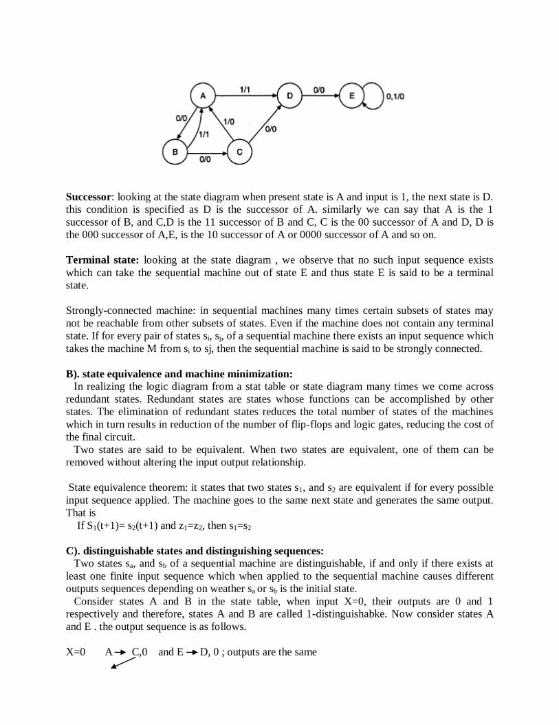
Successor: looking at the state diagram when present state is A and input is 1, the next state is D.
this condition is specified as D is the successor of A. similarly we can say that A is the 1
successor of B, and C,D is the 11 successor of B and C, C is the 00 successor of A and D, D is
the 000 successor of A,E, is the 10 successor of A or 0000 successor of A and so on.
Terminal state: looking at the state diagram , we observe that no such input sequence exists
which can take the sequential machine out of state E and thus state E is said to be a terminal
state.
Strongly-connected machine: in sequential machines many times certain subsets of states may
not be reachable from other subsets of states. Even if the machine does not contain any terminal
state. If for every pair of states si, sj, of a sequential machine there exists an input sequence which
takes the machine M from si to sj, then the sequential machine is said to be strongly connected.
B). state equivalence and machine minimization:
In realizing the logic diagram from a stat table or state diagram many times we come across
redundant states. Redundant states are states whose functions can be accomplished by other
states. The elimination of redundant states reduces the total number of states of the machines
which in turn results in reduction of the number of flip-flops and logic gates, reducing the cost of
the final circuit.
Two states are said to be equivalent. When two states are equivalent, one of them can be
removed without altering the input output relationship.
State equivalence theorem: it states that two states s1, and s2 are equivalent if for every possible
input sequence applied. The machine goes to the same next state and generates the same output.
That is
If S1(t+1)= s2(t+1) and z1=z2, then s1=s2
C). distinguishable states and distinguishing sequences:
Two states sa, and sb of a sequential machine are distinguishable, if and only if there exists at
least one finite input sequence which when applied to the sequential machine causes different
outputs sequences depending on weather sa or sb is the initial state.
Consider states A and B in the state table, when input X=0, their outputs are 0 and 1
respectively and therefore, states A and B are called 1-distinguishabke. Now consider states A
and E . the output sequence is as follows.
X=0 A C,0 and E D, 0 ; outputs are the same
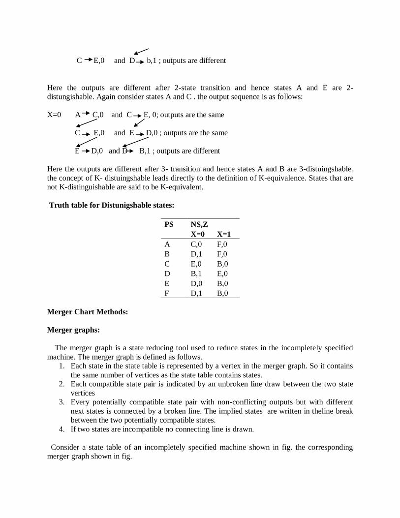
C E,0 and D b,1 ; outputs are different
Here the outputs are different after 2-state transition and hence states A and E are 2-
distungishable. Again consider states A and C . the output sequence is as follows:
X=0 A C,0 and C E, 0; outputs are the same
C E,0 and E D,0 ; outputs are the same
E D,0 and D B,1 ; outputs are different
Here the outputs are different after 3- transition and hence states A and B are 3-distuingshable.
the concept of K- distuingshable leads directly to the definition of K-equivalence. States that are
not K-distinguishable are said to be K-equivalent.
Truth table for Distunigshable states:
PS NS,Z
X=0 X=1
A C,0 F,0
B D,1 F,0
C E,0 B,0
D B,1 E,0
E D,0 B,0
F D,1 B,0
Merger Chart Methods:
Merger graphs:
The merger graph is a state reducing tool used to reduce states in the incompletely specified
machine. The merger graph is defined as follows.
1. Each state in the state table is represented by a vertex in the merger graph. So it contains
the same number of vertices as the state table contains states.
2. Each compatible state pair is indicated by an unbroken line draw between the two state
vertices
3. Every potentially compatible state pair with non-conflicting outputs but with different
next states is connected by a broken line. The implied states are written in theline break
between the two potentially compatible states.
4. If two states are incompatible no connecting line is drawn.
Consider a state table of an incompletely specified machine shown in fig. the corresponding
merger graph shown in fig.
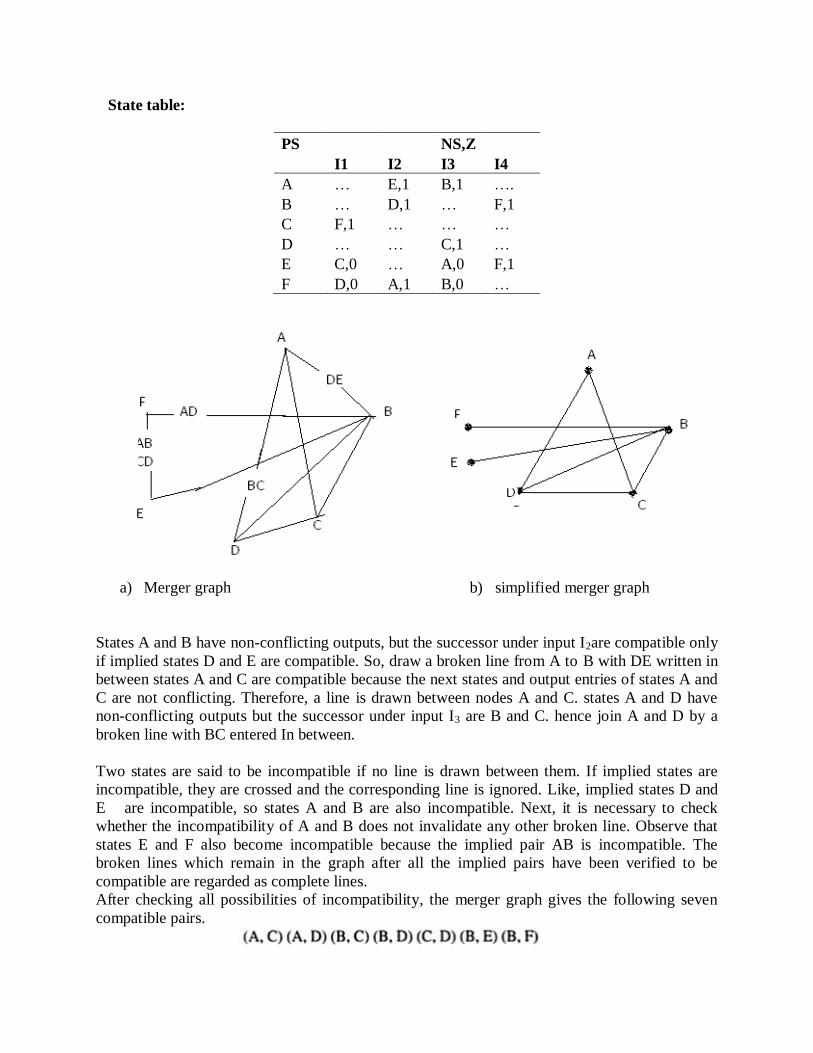
State table:
PS NS,Z
I1 I2 I3 I4
A … E,1 B,1 ….
B … D,1 … F,1
C F,1 … … …
D … … C,1 …
E C,0 … A,0 F,1
F D,0 A,1 B,0 …
a) Merger graph b) simplified merger graph
States A and B have non-conflicting outputs, but the successor under input I2are compatible only
if implied states D and E are compatible. So, draw a broken line from A to B with DE written in
between states A and C are compatible because the next states and output entries of states A and
C are not conflicting. Therefore, a line is drawn between nodes A and C. states A and D have
non-conflicting outputs but the successor under input I3 are B and C. hence join A and D by a
broken line with BC entered In between.
Two states are said to be incompatible if no line is drawn between them. If implied states are
incompatible, they are crossed and the corresponding line is ignored. Like, implied states D and
E are incompatible, so states A and B are also incompatible. Next, it is necessary to check
whether the incompatibility of A and B does not invalidate any other broken line. Observe that
states E and F also become incompatible because the implied pair AB is incompatible. The
broken lines which remain in the graph after all the implied pairs have been verified to be
compatible are regarded as complete lines.
After checking all possibilities of incompatibility, the merger graph gives the following seven
compatible pairs.
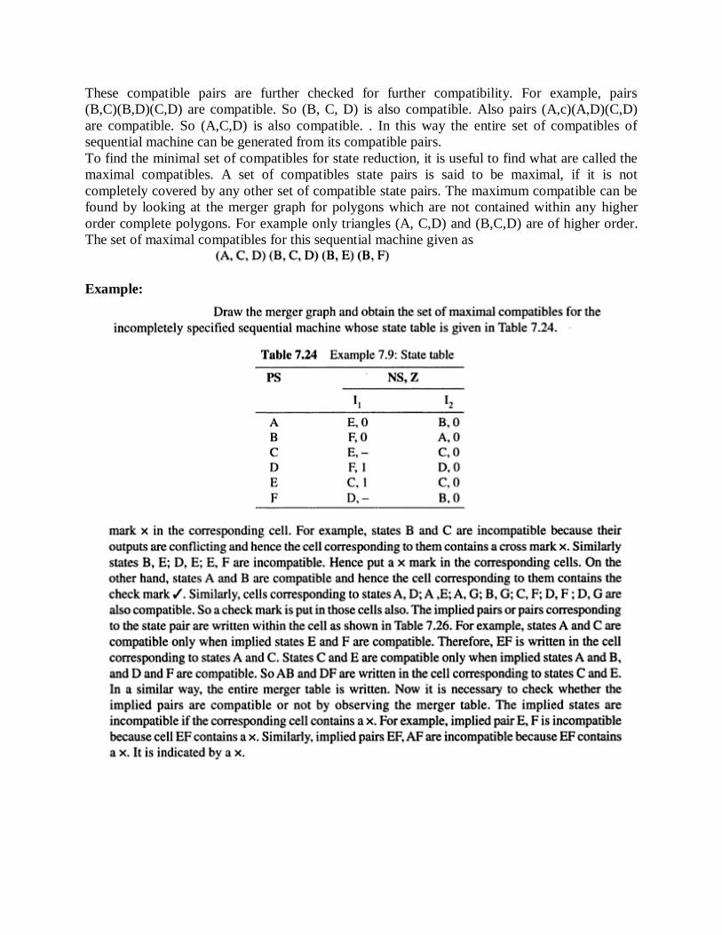
These compatible pairs are further checked for further compatibility. For example, pairs
(B,C)(B,D)(C,D) are compatible. So (B, C, D) is also compatible. Also pairs (A,c)(A,D)(C,D)
are compatible. So (A,C,D) is also compatible. . In this way the entire set of compatibles of
sequential machine can be generated from its compatible pairs.
To find the minimal set of compatibles for state reduction, it is useful to find what are called the
maximal compatibles. A set of compatibles state pairs is said to be maximal, if it is not
completely covered by any other set of compatible state pairs. The maximum compatible can be
found by looking at the merger graph for polygons which are not contained within any higher
order complete polygons. For example only triangles (A, C,D) and (B,C,D) are of higher order.
The set of maximal compatibles for this sequential machine given as
Example:
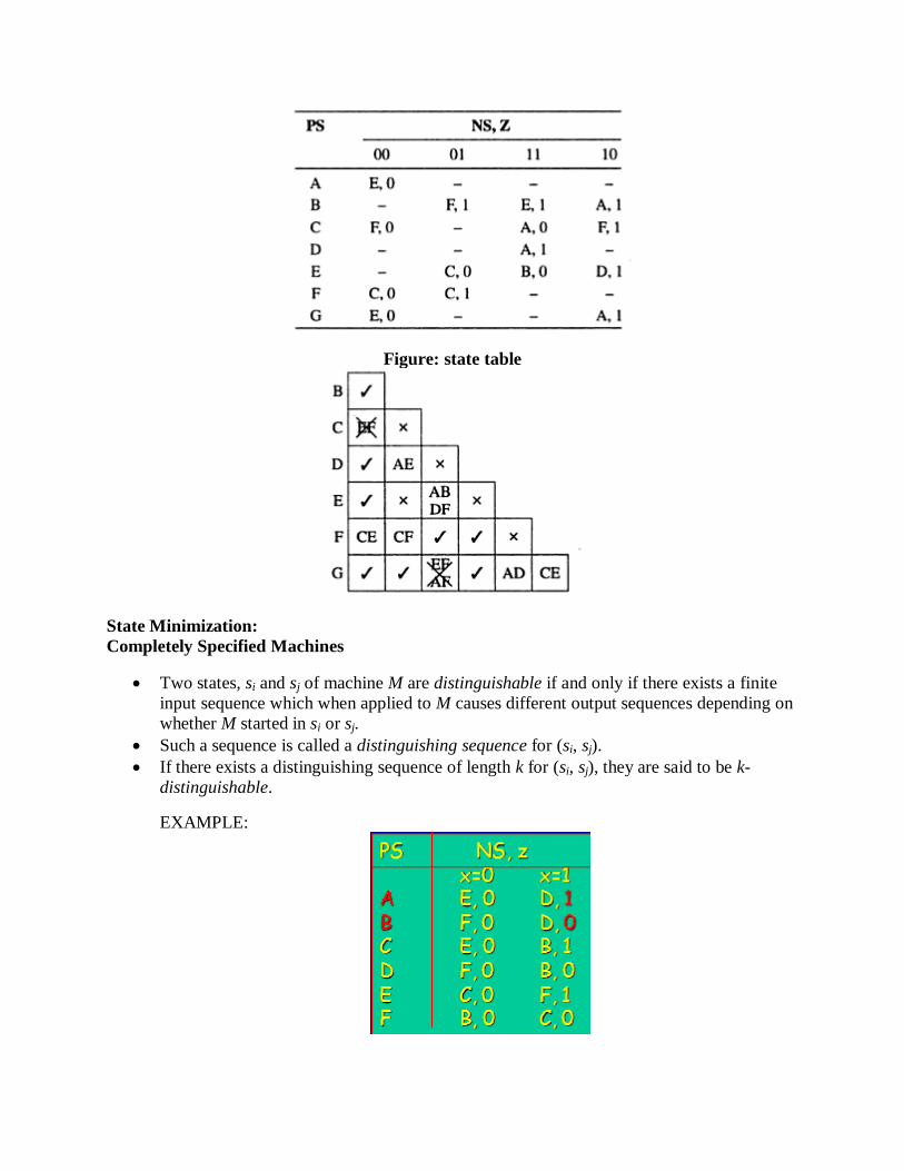
Figure: state table
State Minimization:
Completely Specified Machines
Two states, si and sj of machine M are distinguishable if and only if there exists a finite
input sequence which when applied to M causes different output sequences depending on
whether M started in si or sj.
Such a sequence is called a distinguishing sequence for (si, sj).
If there exists a distinguishing sequence of length k for (si, sj), they are said to be k-
distinguishable.
EXAMPLE:
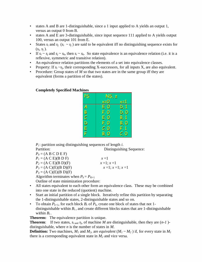
• states A and B are 1-distinguishable, since a 1 input applied to A yields an output 1,
versus an output 0 from B.
• states A and E are 3-distinguishable, since input sequence 111 applied to A yields output
100, versus an output 101 from E.
• States si and sj (si ~ sj ) are said to be equivalent iff no distinguishing sequence exists for
(si, sj ).
• If si ~ sj and sj ~ sk, then si ~ sk. So state equivalence is an equivalence relation (i.e. it is a
reflexive, symmetric and transitive relation).
• An equivalence relation partitions the elements of a set into equivalence classes.
• Property: If si ~sj, their corresponding X-successors, for all inputs X, are also equivalent.
• Procedure: Group states of M so that two states are in the same group iff they are
equivalent (forms a partition of the states).
Completely Specified Machines
Pi : partition using distinguishing sequences of length i.
Partition: Distinguishing Sequence:
P0 = (A B C D E F)
P1 = (A C E)(B D F) x =1
P2 = (A C E)(B D)(F) x =1; x =1
P3 = (A C)(E)(B D)(F) x =1; x =1; x =1
P4 = (A C)(E)(B D)(F)
Algorithm terminates when Pk = PK+1
Outline of state minimization procedure:
• All states equivalent to each other form an equivalence class. These may be combined
into one state in the reduced (quotient) machine.
• Start an initial partition of a single block. Iteratively refine this partition by separating
the 1-distinguishable states, 2-distinguishable states and so on.
• To obtain Pk+1, for each block Bi of Pk, create one block of states that not 1-
distinguishable within Bi , and create different blocks states that are 1-distinguishable
within Bi .
Theorem: The equivalence partition is unique.
Theorem: If two states, si and sj, of machine M are distinguishable, then they are (n-1 )-
distinguishable, where n is the number of states in M.
Definition: Two machines, M1 and M2, are equivalent (M1 ~ M2 ) if, for every state in M1
there is a corresponding equivalent state in M2 and vice versa.
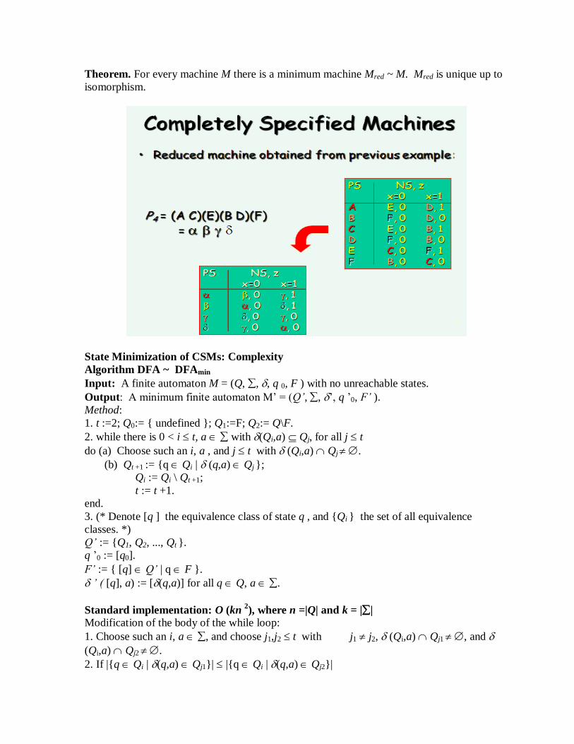
Theorem. For every machine M there is a minimum machine Mred ~ M. Mred is unique up to
isomorphism.
State Minimization of CSMs: Complexity
Algorithm DFA ~ DFAmin
Input: A finite automaton M = (Q, , , q 0, F ) with no unreachable states.
Output: A minimum finite automaton M‘ = (Q’, , ‘, q ‘0, F’ ).
Method:
1. t :=2; Q0:= { undefined }; Q1:=F; Q2:= Q\F.
2. while there is 0 < i t, a with (Qi,a) Qj, for all j t
do (a) Choose such an i, a , and j t with (Qi,a) Qj .
(b) Qt +1 := {q Qi | (q,a) Qj };
Qi := Qi \ Qt +1;
t := t +1.
end.
3. (* Denote [q ] the equivalence class of state q , and {Qi } the set of all equivalence
classes. *)
Q’ := {Q1, Q2, ..., Qt }.
q ‘0 := [q0].
F’ := { [q] Q’ | q F }.
’ ( [q], a) := [(q,a)] for all q Q, a .
Standard implementation: O (kn 2), where n =|Q| and k = ||
Modification of the body of the while loop:
1. Choose such an i, a , and choose j1,j2 t with j1 j2, (Qi,a) Qj1 , and
(Qi,a) Qj2 .
2. If |{q Qi | (q,a) Qj1}| |{q Qi | (q,a) Qj2}|
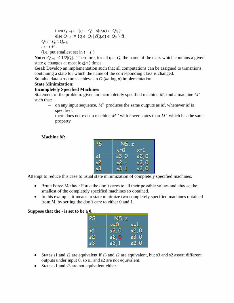
then Qt +1 := {q Qi | (q,a) Qj1 }
else Qt +1 := {q Qi | (q,a) Qj2 } fI;
Qi := Qi \ Qt+1;
t := t +1.
(i.e. put smallest set in t +1 )
Note: |Qt +1| 1/2|Qi|. Therefore, for all q Q, the name of the class which contains a given
state q changes at most log(n ) times.
Goal: Develop an implementation such that all computations can be assigned to transitions
containing a state for which the name of the corresponding class is changed.
Suitable data structures achieve an O (kn log n) implementation.
State Minimization:
Incompletely Specified Machines
Statement of the problem: given an incompletely specified machine M, find a machine M’
such that:
– on any input sequence, M’ produces the same outputs as M, whenever M is
specified.
– there does not exist a machine M’’ with fewer states than M’ which has the same
property
Machine M:
Attempt to reduce this case to usual state minimization of completely specified machines.
Brute Force Method: Force the don‘t cares to all their possible values and choose the
smallest of the completely specified machines so obtained.
In this example, it means to state minimize two completely specified machines obtained
from M, by setting the don‘t care to either 0 and 1.
Suppose that the - is set to be a 0.
States s1 and s2 are equivalent if s3 and s2 are equivalent, but s3 and s2 assert different
outputs under input 0, so s1 and s2 are not equivalent.
States s1 and s3 are not equivalent either.
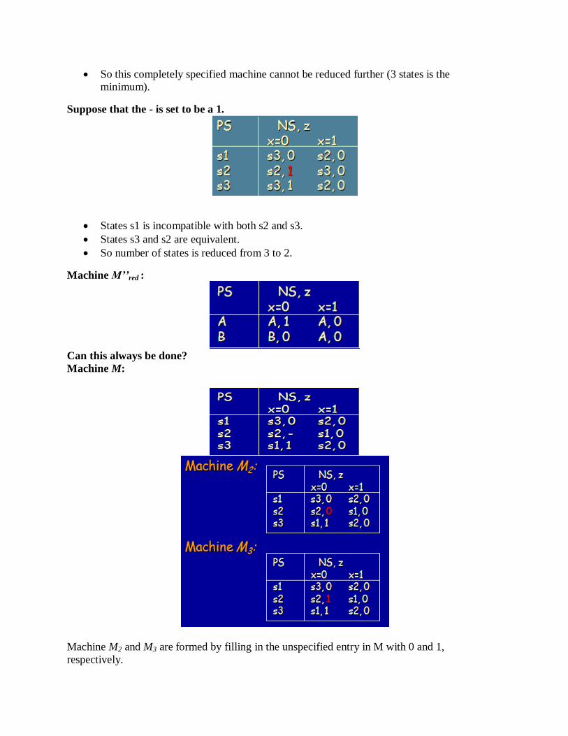
So this completely specified machine cannot be reduced further (3 states is the
minimum).
Suppose that the - is set to be a 1.
States s1 is incompatible with both s2 and s3.
States s3 and s2 are equivalent.
So number of states is reduced from 3 to 2.
Machine M’’red :
Can this always be done?
Machine M:
Machine M2 and M3 are formed by filling in the unspecified entry in M with 0 and 1,
respectively.
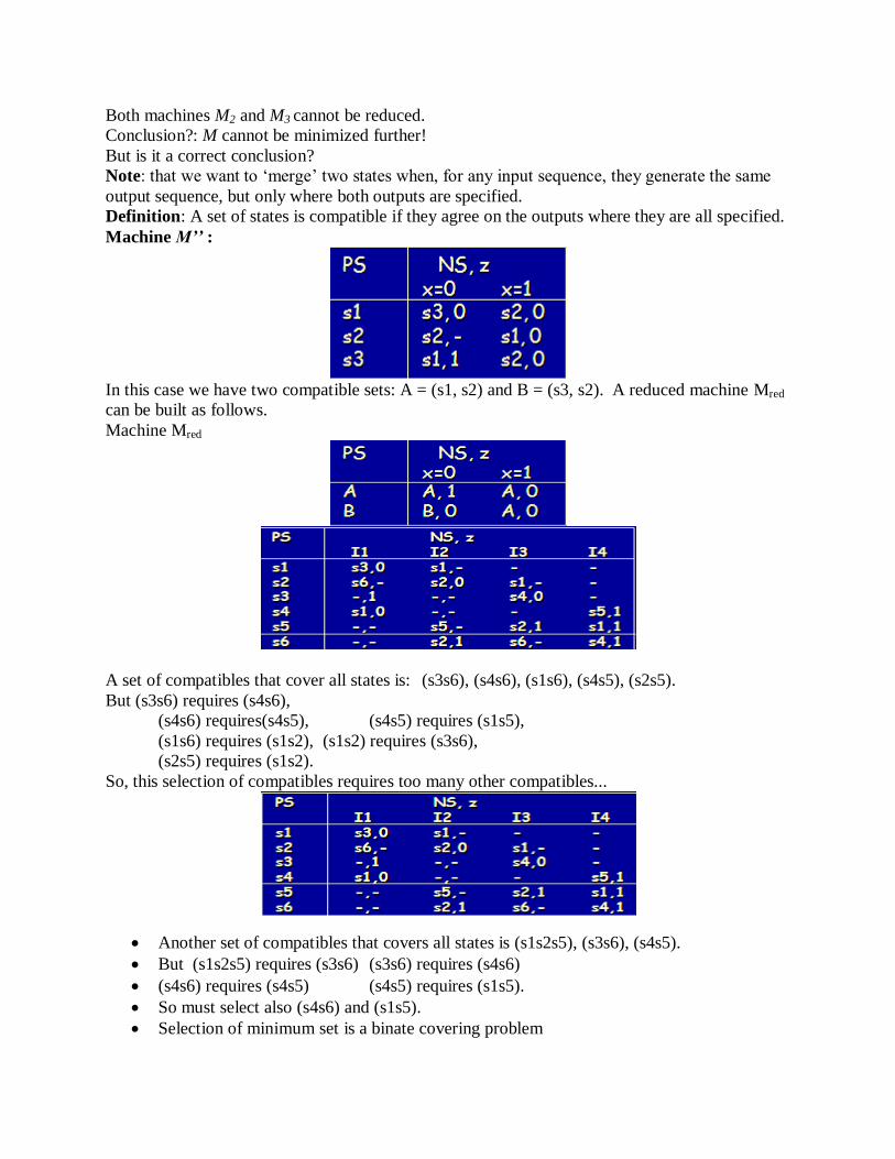
Both machines M2 and M3 cannot be reduced.
Conclusion?: M cannot be minimized further!
But is it a correct conclusion?
Note: that we want to ‗merge‘ two states when, for any input sequence, they generate the same
output sequence, but only where both outputs are specified.
Definition: A set of states is compatible if they agree on the outputs where they are all specified.
Machine M’’ :
In this case we have two compatible sets: A = (s1, s2) and B = (s3, s2). A reduced machine Mred
can be built as follows.
Machine Mred
A set of compatibles that cover all states is: (s3s6), (s4s6), (s1s6), (s4s5), (s2s5).
But (s3s6) requires (s4s6),
(s4s6) requires(s4s5), (s4s5) requires (s1s5),
(s1s6) requires (s1s2), (s1s2) requires (s3s6),
(s2s5) requires (s1s2).
So, this selection of compatibles requires too many other compatibles...
Another set of compatibles that covers all states is (s1s2s5), (s3s6), (s4s5).
But (s1s2s5) requires (s3s6) (s3s6) requires (s4s6)
(s4s6) requires (s4s5) (s4s5) requires (s1s5).
So must select also (s4s6) and (s1s5).
Selection of minimum set is a binate covering problem
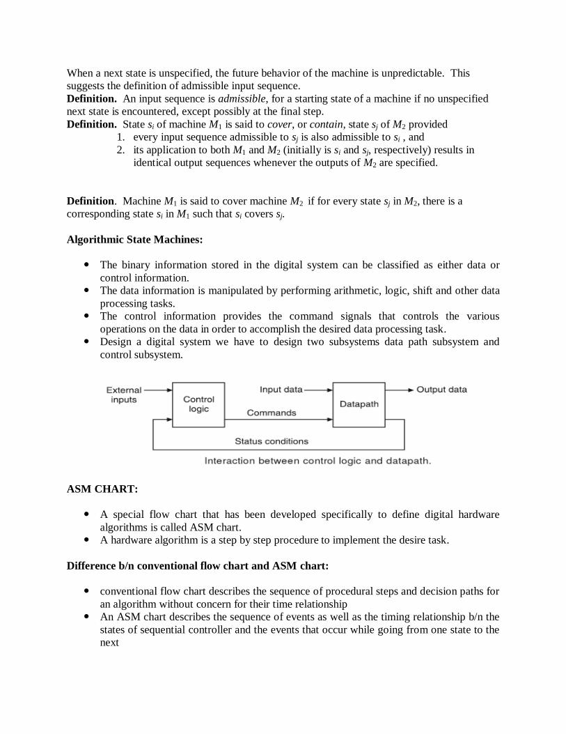
When a next state is unspecified, the future behavior of the machine is unpredictable. This
suggests the definition of admissible input sequence.
Definition. An input sequence is admissible, for a starting state of a machine if no unspecified
next state is encountered, except possibly at the final step.
Definition. State si of machine M1 is said to cover, or contain, state sj of M2 provided
1. every input sequence admissible to sj is also admissible to si , and
2. its application to both M1 and M2 (initially is si and sj, respectively) results in
identical output sequences whenever the outputs of M2 are specified.
Definition. Machine M1 is said to cover machine M2 if for every state sj in M2, there is a
corresponding state si in M1 such that si covers sj.
Algorithmic State Machines:
The binary information stored in the digital system can be classified as either data or
control information.
The data information is manipulated by performing arithmetic, logic, shift and other data
processing tasks.
The control information provides the command signals that controls the various
operations on the data in order to accomplish the desired data processing task.
Design a digital system we have to design two subsystems data path subsystem and
control subsystem.
ASM CHART:
A special flow chart that has been developed specifically to define digital hardware
algorithms is called ASM chart.
A hardware algorithm is a step by step procedure to implement the desire task.
Difference b/n conventional flow chart and ASM chart:
conventional flow chart describes the sequence of procedural steps and decision paths for
an algorithm without concern for their time relationship
An ASM chart describes the sequence of events as well as the timing relationship b/n the
states of sequential controller and the events that occur while going from one state to the
next
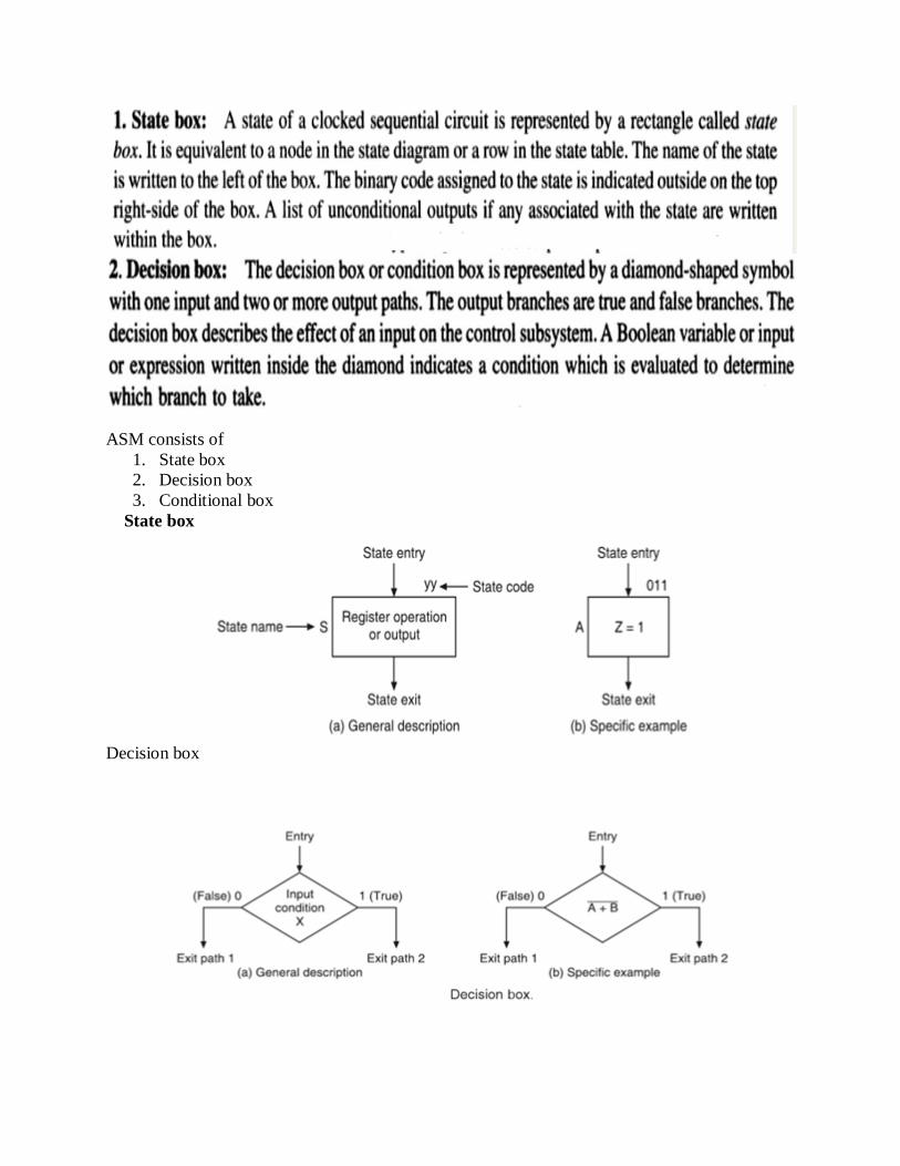
ASM consists of
1. State box
2. Decision box
3. Conditional box
State box
Decision box
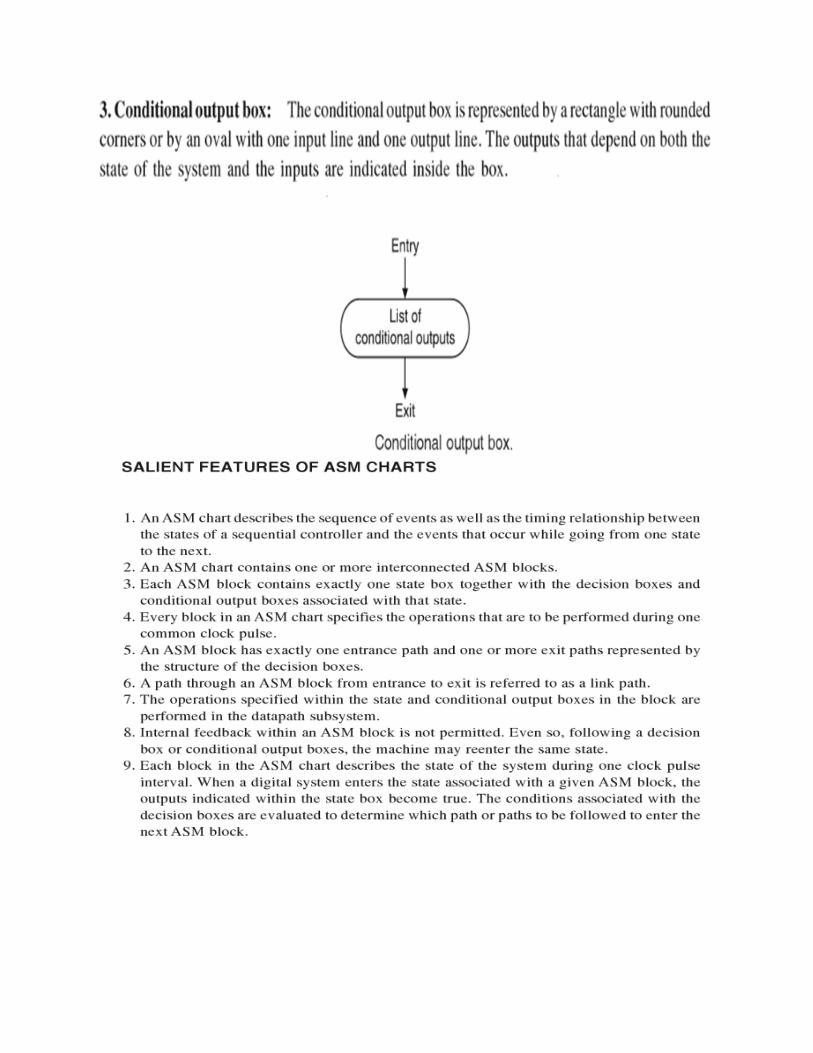
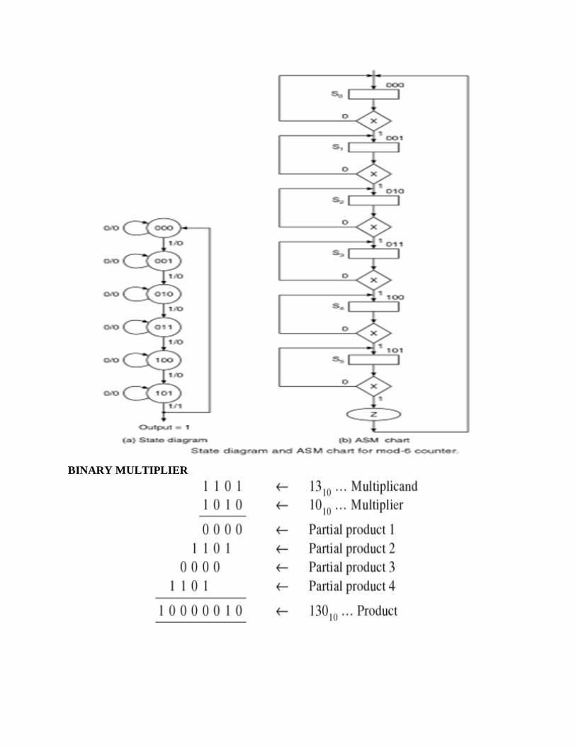
BINARY MULTIPLIER
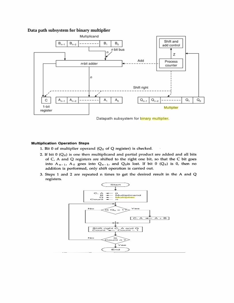
Data path subsystem for binary multiplier