surface and thin film analysis with electron and …surface and thin film analysis with electron and...
TRANSCRIPT

Surface and Thin Film Analysis with Electron and Mass Spectrometric Techniques
A. Wucher
Fachbereich Physik, Universität Kaiserslautern
D-67653 Kaiserslautern
Abstract
We give a short overview of recent analytical techniques for compositional surface analysis and the determination of concentration depth profiles. More specifically, the principle, the instrumentation and the performance of the routinely used electron spectroscopic and mass spectrometric methods, namely Photo- and Auger Electron Spectroscopy PES and AES, resp. Secondary Ion and Secondary Neutral Mass Spectrometry SIMS and SNMS, are described. The application of these techniques to the analysis of thin film structures is demonstrated by corresponding practical examples. The potentialities of the different techniques are specifically addressed with regard to the quantitation of the measured data, detection limits for trace analysis as well as the spatial resolution both in directions parallel and perpendicular to the sample surface.
1. General overview
With decreasing dimensions and increasing sophistication of the architecture of thin films and multilayer structures the traditional techniques for the chemical characterization of materials have to be substituted by such techniques which combine quantitative chemical analysis with high spatial, i. e. lateral and depth resolution. Moreover, the precise characterization of the substrate surface on which a layer structure is deposited is a necessary prerequisite for guaranteeing the desired qualities - as, for instance, the adhesion - of a coating,. In particular, detailed knowledge about the interfaces to the substrate and within a layered structure is decisive in order to ensure the functional properties of a thin film structure.
The respective information can be supplied by analytical techniques which have evolved from the field of surface physics. Such methods are based on the excitation of surface

sensitive analytical signals through the interaction of photons, electrons or ions with the outermost atomic layers of a sample. We distinguish, in particular, between two main groups, namely
- electron spectroscopic techniques such as photoelectron or Auger electron spectroscopy PES or AES, in which the analytical information is derived from the kinetic energy distribution of electrons released from surface atoms or surface near electronic bands, and
- mass spectrometric methods such as secondary ion or secondary neutral mass spectrometry SIMS or SNMS characterizing charged or neutral atoms and molecules released from the sample surface.
Besides these methods a wealth of other techniques for the chemical and structural characterization of solid surfaces have been developed (see, for example, refs. 1-6). For instance, the spectral characterization of photons emitted during the ion bombardment of a surface can deliver useful information about the surface near composition (Bombardment induced Light Emission BLE /7/). Backscattering methods derive the mass of surface particles from the loss of kinetic energy which impinging and subsequently backscattered particles experience during their interaction with the surface (Rutherford Backscattering Spectroscopy RBS /8/). Detailed chemical information about the short range atomic order or even the atomic neighborhood conditions in a solid are delivered by a careful inspection of the fine structure of X-ray absorption edges (Extended X-ray Absorption Fine Structure EXAFS /9/). In addition, the fluorescence induced by X-ray absorption can be used to identify atomic species within the sample, and by utilizing the total reflection of the incoming radiation this technique can be made quite surface sensitive (Total Reflection X-Ray Fluorescence TXRF /10/). Recent scanning probe techniques such as Scanning Tunneling Microscopy STM or Atomic Force Microscopy AFM do not only supply information about the nanostructural or even the atomic order of surfaces, but deliver to some extent also local chemical information when being operated in a spectroscopic mode /11/. In this paper, however, we will concentrate on such techniques for chemical surface analysis which are now widely used and therefore have become the workhorses of modern thin film analysis..
In principle, the analytical techniques mentioned above can be used with high lateral resolution, i. e. resolution in the direction parallel to the surface, by tightly focusing the excitation beam and raster scanning it over the investigated surface. With this so-called microprobe technique, chemical maps of the surface composition can be obtained with

sub-micron lateral resolution. In addition, some methods can be used in the so-called microscope mode, where the excitation beam is defocused and the analytical signal itself is used to produce a stigmatic image of the surface.
The complete three-dimensional analysis of thin films becomes possible when such methods are combined with an appropriate microsectioning technique /12/. Besides mechanical bevelling methods such as, for instance, a well defined grinding with a rotating sphere, the controlled sputter removal of the surface by low energy ion bombardment has become the most widely applied method in that context. Under careful operation, sputter erosion enables compositional depth profile analysis almost along an atomic scale.
When ion sputtering is employed either for depth profiling or to remove contamination layers from the surface to be analyzed, an important difference between the above mentioned groups of analytical techniques has to be mentioned: While the electron spectroscopic techniques detect what is left at the surface after it has been attacked by the ion bombardment, the signals obtained with the mass spectrometric techniques refer to those particles which are removed from the surface. The analytical information obtained with either of these techniques may therefore differ considerably, since a preferential removal of certain species from the surface by the ion bombardment may sometimes cause drastic deviations from the original surface composition. In that respect, a mass spectrometric method collecting the removed surface particles with specific, but well defined detection probabilities may be more beneficial.
As another general aspect, the large differences between the detection power of the individual techniques have to be considered: Electron spectroscopic methods as AES or PES are in general restricted to a detection power of at best several tenths of an atomic percent, i.e. a concentration between 10-2 and 10-3 of the desired element at the surface. In contrast, mass spectrometric surface analytical techniques usually provide detection powers in the ppm range; sophisticated SIMS or SNMS instruments are even capable to detect trace element concentrations down to the ppb regime.
In all analytical techniques being dealt with here an electrical charge is either brought to or removed from the sample surface via the probing or the detected species. Therefore, special additional measures have to be implemented for the analysis of an electrically non- or poorly conducting substrate, or when the investigated coating consists entirely or in part of dielectric material. In order to make surface analytical techniques, especially in conjunction with sputter depth profiling, applicable to such sample structures, emphasis

must be paid on how to compensate any surface charging which would deteriorate either the characteristic electron energies in Auger or Photoelectron spectroscopy or prevent any controlled sputter removal by decelerating the bombarding ions.
In the following sections, the physical background as well as the experimental setup and measurement procedure of the different analytical techniques will be described, particularly with regard to their application to thin film structures. In some cases, recent methodical progress which is not yet included in available textbooks or reviews on surface and thin film analysis will be addressed. In addition, the surface sensitive character of the electron and mass spectrometric techniques will be discussed as well as the possibilities for lateral imaging and high resolution sputter depth profiling.
2. Electron spectroscopic methods for surface analysis
2.1 Photoelectron Spectroscopy PES
2.1.1 Physical background and instrumentation
The basic mechanisms for electron emission stimulated by photon or electron irradiation are schematically shown in Fig. 1. The PES signals result from the photoionization process in a certain energy level in the atomic core, a valence band or the conduction band. An ionization in a core level is generally followed by a re-arrangement of the electronic structure which may lead to the emission of an Auger electron in a radiationless process. Therefore, in electron energy spectra resulting from the irradiation with photons of sufficient energy (soft X-rays) Auger electron peaks do always appear besides the photoelectron peaks. Since Auger electron emission is independent of the kind of the primary ionization event, photoelectron peaks can be readily discriminated against the Auger peaks by a variation of the energy of the irradiating photons.

Depending on the energy of the incident photons and, hence, the regime of the electron binding energy which is probed, we distinguish between Ultraviolet Photoelectron Spectroscopy UPS and X-ray induced Photoelectron Spectroscopy XPS. While UPS, employing photon energies of 10 - 40 eV, has become an important tool for the determination of electronic band structures and the characterization of adsorbate systems, XPS using in general the excitation with the Mg-Kα 1,2-line (1253.6 eV) or the Al-Kα 1,2-line (1486 eV) probes element specific electronic core levels (and was hence originally denoted as Electron Spectroscopy for Chemical Analysis ESCA). As an important condition for the identification of specific electron binding energies Eb the line width is sufficiently small in both cases (0.7 and 0.85 eV, respectively).
Fig. 2 shows the principal setup of an XPS apparatus. Besides the photon source - a low energy, sometimes monochromated X-ray tube - an electrostatic energy analyzer with an electron counting system is the other essential component of a PES-apparatus. Most frequently a hemispherical analyzer is used. According to Fig. 3 the electron energy at the entrance of the analyzer system is given by
Ek = hν - EbF - Φ sp , (1)
where EbF is the respective electron binding energy related to the Fermi level of the
sample material, and Φsp the (fictive) spectrometer work function being a constant of the PES apparatus. For a fixed photon energy hν and after the determination of Φ sp via a standard sample (mostly Au with Eb
F = 83.98 eV for the 4f7/2 electron energy level) the element specific electron binding energies Eb
F can be determined from the measured Ek-values, both varying inversely to each other.
The hemispherical energy analyzer of a PES-apparatus is in general preceded by an electron optical deceleration system by which the electrons are pre-retarded before

entering the analyzer. The complete system can be operated in two modes:
a) In the so-called fixed retardation ratio mode (FRR) the electrons are retarded to the pass energy E0 of the analyzer such that Ek/E0 = const. In this mode the energy resolution ∆ E/E is a constant which can be improved by increasing the retardation ratio Ek/E0. The absolute value of the energy transmission window ∆E and, hence, the analyzer transmission T is proportional to E0 and, hence, to Ek in this case.
b) In the fixed analyzer transmission mode (FAT-mode) the electrons are always decelerated to a fixed pass energy E0 . Quite obviously, this results in a constant absolute energy transmission window ∆E which is determined by the value of E0. Due to the changing deceleration ratio, however, the sample area and solid angle accepted by the secondary electron optics depends on the transmitted energy Ek, and the overall spectrometer transmission T is proportional to E0
2/Ek.
The electron intensity (current) arriving at the counting element (secondary electron multiplier or micro channel plate) is given by Ic∼T ⋅N(E), where N(E) is the height of the electron energy distribution around an energy E. Then, the XPS-signals are proportional to N(Ek) ⋅Ek in the FRR-mode, but to N(Ek)/Ek in the FAT-mode, if the electron deceleration is assumed not to change the original energy distribution.
2.1.2 Quantification of PES
Fig. 4 displays the XPS-spectrum of a contaminated glass surface. The respective measurement was performed in the FAT-mode with a fixed analyzer path energy of 117.4 eV. The Ek-axis has already been transferred into that for the electron binding energy Eb
F according to equ. (1). Apart from the photoelectron peaks (for instance the O1s- or the Na1s-peaks) the spectrum contains Auger electron peaks (O KVV or C KLL) as expected.
The photoelectron signal from a sample that is homogeneous in the analysis volume can be written in a simplified form as

(2)
where T is the analyzer transmission combined with a geometry and efficiency factor of the individual PES instrument, Jp is the incident photon flux density (in general 1012 photons/cm2s), σx the photoionization cross section for the considered orbital of x, λ x the mean escape depth (inelastic mean free path, cf. section 4.1) of the respective photoelectrons and nx the number density of atoms of element x within the sample. In eq. (2), it is assumed that the entire sample surface is illuminated by the photon beam, whereas the analyzed surface area contributing to the measured signal (included in the factor T) is exclusively determined by the electron optical acceptance of the spectrometer. When the factors being characteristic for the excitation of a certain photoelectron peak and the individual apparatus are combined, equ. (2) can be re-written as
nx = IPESx/Sx . (3)
Finally, from the individual ni for all different elements in the analysis volume the concentration of X is obtained as
. (4)

For the quantitation according to equ. (4) Ix (or Ii) has to be taken as the total count rate of the considered photoelectron peak, i.e. the area of the peak after subtracting the background signal in an appropriate way, most simply by a linear interpolation between the two footpoints of the peak. A corresponding evaluation of the XPS-spectrum in Fig. 4 yields, e.g., an oxygen concentration of 30 at% and a carbon concentration of 50 at% at the contaminated surface.
An important aspect of the XPS-method is the possibility to obtain information about the chemical state of an atomic species by a chemical shift of the individual photoelectron peaks. This effect results from the relaxation of the energetic structure of the electron system resulting from the charge transfer to the valence shell of the atom during the formation of a chemical bond. It is this possibility which makes XPS, in particular, useful not only for the compositional characterization but also for the detection of the binding conditions at a sample surface. In a dynamic mode, surface reactions as, e.g. the oxidation process can be monitored. An example is given in Fig. 5 for a variation of the Ta(4f)-peaks when the Ta atoms are bound in different oxide configurations. It is seen that the chemical shift is roughly proportional to the oxidation number of the atoms. Depending on the energy resolution of the electron spectrometer even the individual binding states of C in different hydrocarbons can be detected (see ref. for example).
The application of PES to non-conducting samples does in general not cause serious problems when the photoelectron flux from the sample remains relatively small. Even for a slight charging of the surface XPS-spectra remain evaluable, as the whole spectral structure is just shifted uniformly along the energy axis. In such cases, the chemical characterization of an insulating surface or coating can still be performed in a reliable manner when the energetic differences of the individual photoelectron peaks are used for their identification making use of corresponding tables or handbooks as ref. 13.
2. 2 Auger Electron Spectroscopy

2.2.1 Instrumentation and experimental procedure
According to Fig. 1 three different atomic energy levels (U, V and W) are involved in the formation of an Auger electron, the underlying Auger transition is therefore characterized as UVW. Hence, Auger Electron Spectroscopy AES can identify elements with an atomic number Z≥ 3 (i.e. starting with Li). Recent AES-instruments are mostly based on a so-called cylindrical mirror analyzer CMA (see Fig. 6). Since a CMA accepts the ejected electrons in a 2π -geometry within a cone mantle with a half opening angle of 42.3° , it yields relatively high signal intensities. Other types of electrostatic analyzers are also employed, particularly when AES is combined with in-situ Photoelectron Spectroscopy. Retarding field analyzers can be employed as well, in order to combine chemical analysis with structural surface information from Low Energy Electron Diffraction LEED (cf., e.g. ref. ).
In CMA-based instruments the primary electron gun is generally located inside the inner cylinder of the analyzer, and the exciting electron beam is traveling along the axis of the cylindrical arrangement. Then, the sample can be readily positioned at such a distance from the analyzer entrance for which the optimum entrance conditions for the electron trajectories through the analyzer are achieved. Auger signals are recorded both in a direct mode displaying the electron energy distributions N(E) for the individual peaks, or as differentiated spectra which increase in general the detection sensitivity and enable a simple separation of the background from the "true" secondary electrons by lock-in techniques. CMA-systems are mostly operated without any pre-retardation system, i.e. with ∆E/E = const. Therefore, the Auger intensities measured in the direct mode are proportional to E⋅ N(E) (see also section 2.1).
2.2.2 Quantification of AES
The quantitation of AES follows the same routes as outlined in the preceding section for PES. The signal measured for a species X is given by
, (5)
where Ip now denotes the primary electron current, σi is the cross section for electron impact ionization producing the core hole, and is the probability that this hole is filled by an Auger transition. The factor (1+r) in eq. (5) accounts for the contribution of primary electrons which are elastically backscattered from deeper layers and, hence, cross the surface near region from which Auger electrons can be detected (cf. section 4.1) more than once.
As in the case of X-ray induced photoelectron spectroscopy, the individual Auger electron peaks are identified by a comparison with tabulated values from standard handbook spectra (see ref. 14, for instance). For the determination of the concentration of an element X from a respective characteristic Auger peak equ. (4) can be applied again. Mostly, the sensitivity factors Si which now refer to a certain Auger transition are conveniently replaced by relative sensitivity factors referring all S-values
to that for one reference Auger peak. Thus the individual experimental parameters or their variation during the analysis need not be taken into account separately. As for PES, the areas under the Auger electron peaks have to be determined when the Auger electron spectra are recorded in the direct mode. For the differentiated Auger spectra the peak-to-peak (ptp)-amplitudes are taken as the Auger intensities IX entering equ. (4), since for a fixed shape of the Auger peak these are directly proportional to the areas under the undifferentiated peaks.
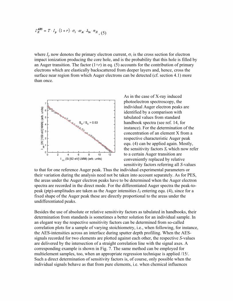
Besides the use of absolute or relative sensitivity factors as tabulated in handbooks, their determination from standards is sometimes a better solution for an individual sample. In an elegant way the respective sensitivity factors can be determined from so-called correlation plots for a sample of varying stoichiometry, i.e., when following, for instance, the AES-intensities across an interface during sputter depth profiling. When the AES-signals recorded for two elements are plotted against each other, the respective S-values are delivered by the intersection of a straight correlation line with the signal axes. A corresponding example is shown in Fig. 7. The same method can be employed for multielement samples, too, when an appropriate regression technique is applied /15/. Such a direct determination of sensitivity factors is, of course, only possible when the individual signals behave as that from pure elements, i.e. when chemical influences

changing peak positions and intensities can be disregarded.
2.2.3 AES-analysis of dielectric samples
While charging effects have been mentioned to be less detrimental in X-ray induced Photoelectron Spectroscopy (section 2.1), they can completely deteriorate the Auger spectra because of the low energies of the signal carrying electrons in this case. AES is, therefore, often considered to be not applicable to electrically non-conducting sample structures. Such difficulties have been shown to be successfully surmounted in the following way /16/:
Quite obviously, no net charging of a dielectric sample occurs when the electron currents to and from the surface compensate each other precisely. Hence, such primary beam parameters have to be selected for which the total secondary electron yield γ, which is known to vary with the energy Ep as shown schematically in Fig. 8, becomes unity. As seen in Fig. 8, a first necessary prerequisite to fulfill this condition is that γ max must be above 1. Secondly, to arrive at stable conditions, the primary beam parameters have to be chosen such that the yield curve γ (Ep) crosses unity with a negative slope, i.e. after having passed through its maximum. If Ep is chosen slightly above the respective value denoted by EII in Fig. 8, the dielectric sample will charge up negatively and thus decelerate the primary electrons back to Ep = EII in a self stabilizing manner. When, on the other side, the primary electron energy Ep is slightly below EII, the positive charge developing at the surface will retain slow secondary electrons and, hence, bring the effective secondary electron yield back to 1 again. It should be noted, that such stable conditions will not establish at EI where the secondary electron yield curve crosses unity
with a positive slope.
Fig. 9 displays the relevant section of an Auger spectrum obtained by this procedure from an α -alumina surface as an example for an almost perfect electrical insulator. The peak positions and the complete appearance of the spectrum is of the same quality as obtained for electrically conducting

samples. In the present example, an Ep-value of 3 keV and an electron incidence angle of 50° against the surface normal had to be selected in order to establish the charge compensating conditions mentioned above.
2.3 Sputter Depth Profiling
If the electron spectrometric methods described in the previous sections are combined with an ion induced sputter erosion of the sample surface, the variation of the sample composition with depth z below the original surface can be determined. The most widely used technique in that respect is AES depth profiling by combining the AES setup with a rare gas ion gun delivering, for instance, Ar+ ions of energies between 1 and 5 keV.
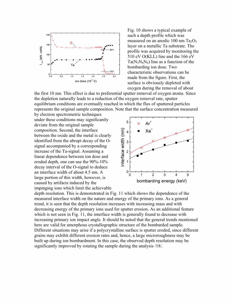
Fig. 10 shows a typical example of such a depth profile which was measured on an anodic 100 nm Ta2O5 layer on a metallic Ta substrate. The profile was acquired by monitoring the 510 eV O(KLL) line and the 166 eV Ta(N5N6N6) line as a function of the bombarding ion dose. Two characteristic observations can be made from the figure. First, the surface is obviously depleted with oxygen during the removal of about
the first 10 nm. This effect is due to preferential sputter removal of oxygen atoms. Since the depletion naturally leads to a reduction of the oxygen removal rate, sputter equilibrium conditions are eventually reached in which the flux of sputtered particles represents the original sample composition. Note that the surface concentration measured by electron spectrometric techniques under these conditions may significantly deviate from the original sample composition. Second, the interface between the oxide and the metal is clearly identified from the abrupt decay of the O- signal accompanied by a corresponding increase of the Ta-signal. Assuming a linear dependence between ion dose and eroded depth, one can use the 90%-10% decay interval of the O-signal to deduce an interface width of about 4.5 nm. A large portion of this width, however, is caused by artifacts induced by the impinging ions which limit the achievable depth resolution. This is demonstrated in Fig. 11 which shows the dependence of the measured interface width on the nature and energy of the primary ions. As a general trend, it is seen that the depth resolution increases with increasing mass and with decreasing energy of the primary ions used for sputter erosion. As an additional feature which is not seen in Fig. 11, the interface width is generally found to decrease with increasing primary ion impact angle. It should be noted that the general trends mentioned here are valid for amorphous crystallographic structure of the bombarded sample. Different situations may arise if a polycrystalline surface is sputter eroded, since different grains may exhibit different erosion rates and, hence, a large microroughness may be built up during ion bombardment. In this case, the observed depth resolution may be significantly improved by rotating the sample during the analysis /18/.

3. Mass spectrometric analysis of surfaces and thin film structures
Quite generally, the surface analytical techniques discussed in the following section are based on the mass spectrometric analysis of particles removed from the surface under investigation. In all practical realizations of this method, the particles are released from the surface by ion sputtering. An important quantity describing the sputtering process is the total sputtering yield Ytot, which is defined as the average number of atoms ejected from the surface by one impinging primary ion. In order to establish a composition analysis of surfaces consisting of more than one atomic species, it is necessary to define the partial sputtering yield Yx which is characteristic of a certain sputtered species X. Under conditions where the sputtered material consists almost exclusively of atoms, the sum of all YX must naturally equal Ytot. If the surface is bombarded with an ion dose sufficient to establish sputter equilibrium conditions, the surface material must be removed stoichoimetrically, i. e. the contribution of YX to Ytot must represent the atomic concentration of the element X in the sample. It is therefore the goal of the techniques described in the following subsections to determine YX from a mass spectrum of the sputtered particles. For this purpose, however, the sputtered species must be ionized in order to render them accessible to mass spectrometric detection. It is basically the way in which ionization is achieved in which the two techniques discussed in the following subsections differ.
3.1 Secondary Ion Mass Spectrometry SIMS
In SIMS, one takes advantage of the fact that a certain, in most cases relatively small fraction of the sputtered particles are emitted in a charged state. The mass resolved detection of these so-called secondary ions form the basis of the SIMS technique.
3.1.1 Instrumentation and Experimental Procedure
The standard components of a SIMS apparatus are shown in Fig. 12. They consist of an ion gun delivering the primary ions, a mass spectrometer for mass-to-charge separation and an ion detector (secondary electron

multiplier, channeltron or microchannel plate) designed for single ion detection. The primary ion gun is either operated with rare gas ions or with chemically reactive ions like O2
+ or Cs+ in order to enhance the secondary ion formation probability (cf. section 3.1.2), typical bombarding energies range from 1 keV to about 20 keV. In general, three different types of mass spectrometers are used: The quadrupole mass spectrometer provides a low cost instrument and can be routinely operated at about unit mass resolution. Its major drawback is the relatively low transmission which, in addition, may be significantly mass dependent. The double focusing mass spectrometer combining an electrostatic deflector with a magnetic sector provides a much higher mass resolution and transmission, and is therefore used in today's state-of-the-art SIMS microprobe instrumentation. A third variant, which has become commercially available only recently, employs a pulsed primary ion beam in combination with time-of-flight mass spectrometry of the secondary ions (TOF-SIMS). The main advantage of the latter technique is given by the parallel detection of all masses as well as the in principle unlimited mass range. In combination with high brightness liquid metal ion guns, the SIMS technique can be used for mass spectrometric surface characterization with sub-micron lateral resolution. As an example of such an analysis, Fig. 13 shows TOF-SIMS images of a copper grid which was placed on an aluminum substrate. Besides the signals characteristic for specific atomic secondary ions representing either the matrix material (Cu+, Al+) or trace impurities in the grid material (Na+, S+), the figure also shows an image which is obtained by registrating the electrons released from the surface by ion bombardment. From the cross section of this image, which represents the ion induced counterpart to the scanning electron microscope technique, the sub-micron lateral
resolution is clearly demonstrated.
The application of Secondary Ion Mass Spectrometry SIMS to non-conducting samples becomes difficult for twofold reasons: Firstly, considerable charge is
transferred to the sample by the primary ion beam, and secondly the kinetic energy of the analyzed positive or negative secondary ions are strongly influenced by any sample charging. This may considerably affect the secondary ion signals, e.g. via energy dependent effects on the transmission of the mass spectrometer. Recent SIMS instruments contain, therefore, an additional low energy electron gun, from which charge compensating electrons are conducted to the analyzed surface area. Thus, SIMS can be applied to non-conducting samples, too.

3.1.2 Quantification of SIMS
The SIMS signal measured for a specific sputtered species X, i. e. the number of X+ or X- secondary ions registrated per unit time, is given by
. (6)
Ip stands for the bombarding ion current and ηx for the detection efficiency of an emitted secondary ion X+,-. As mentioned above, the important quantity carrying the analytical information is the partial sputtering yield YX which for atomic sputtering under steady state conditions can be expressed as
. (7)

The major problem of SIMS quantitation is induced by the secondary ion formation
probability , i. e. the probability that a sputtered particle X leaves the surface in either a positively or negatively charged state. Due to the fact that the ionization process occurs at the surface and is therefore directly coupled to the sputtering process, this quantity strongly depends on the chemical environment the particle is ejected from. In
many cases, this may lead to large variations of for the same species X+,- even by orders of magnitude, depending on the composition of the surface. A particularly
common example is displayed in Fig. 14, which shows that a coverage of a clean metallic sample by electronegative atoms like oxygen may drastically increase the formation probability of positive secondary ions, similar enhancements are observed for the negative ions if the surface is partly covered with electropositive species
like Cs. It is evident that such matrix effects are detrimental to a quantitative determination of the surface composition itself. Therefore, in many cases SIMS must be considered to deliver only qualitative information about the true composition of the sample surface. It is, however, an extremely powerful tool to determine the trace concentration of elements in non-varying matrices, for instance in the analysis of dopant profiles in semiconductors, with detection powers down to the ppb level. Fig. 15 shows such an analysis for a Boron profile in Si which was generated by implantation of B+ ions
into a silicon substrate. During the analysis the sample was bombarded with 8 keV O2
+ ions and the signal of B+ secondary ions was monitored.
3.2 Surface analysis by MCs+-ions
When a Cs+-ion beam is applied to a surface to be analyzed, MCs+ ions are

detected in the particle flux from the sample besides atomic and other molecular ions. Quite recently, the formation of MCs+ ions, where M stands for an elemental constituent of the sample, has been shown to be controlled by a combination process between a backscattered or re-ejected Cs+-ion and a simultaneously sputtered neutral atom, i.e. by
. (8)
Evidence for this process results clearly from a strong correlation between the MCs+-intensities and the atomic polarizability of M0 for a large number of elements /20/. The Cs+-ion polarizes a simultaneously ejected neutral surface atom and the respective MCs+-ion is formed by an ion-dipole interaction. The still very close surface may act as a third partner which accepts a part of the excess energy from the respective combination process.
Since the flux of sputtered neutral surface atoms is known to be insensitive to the matrix effects in secondary ion emission, the formation mechanism described by equ. (8) is expected to be less sensitive to the actual chemical surface conditions. Hence, the MCs+-signals should provide a much better quantifiability than ordinary atomic SIMS-signals. Such a behavior has indeed been confirmed by a number of recent applications of the MCs+-method. An example is given in Fig. 16, where the intensities of atomic (M+) and molecular (MCs+) secondary ions measured on an InP sample are monitored as a function of the oxygen coverage of the surface /21/. It is seen that the oxygen matrix effect which is very pronounced for In+ is practically absent for InCs+. Instead, the InCs+ signal decreases at high oxygen coverages due to the decreasing surface concentration of In. Residual effects are essentially due to the influence of the actual surface conditions onto the formation of the Cs+-ions controlling the combination process according to equ. (8). Hence, quantitative surface analysis with the MCs+-method becomes possible with a relatively good reliability.
3.3 Secondary Neutral Mass Spectrometry SNMS
It is well established that in most cases, even for ionic target materials such as metal oxides, secondary ions contribute only by a fraction up to some 10-2 to the particle flux

released under ion bombardment. Hence, the vast majority of sputter removed particles consists of neutral atoms and molecules. The flux of sputter ejected secondary neutrals, therefore, reflects the true surface composition, even when the secondary ion signals vary by orders of magnitude with changing chemical conditions at the sample surface. However, in order to allow their mass spectrometric identification, the ejected neutrals must be postionized subsequent to their sputter removal from the surface. In contrast to SIMS, where particle ejection and ionization occur in the same event, in SNMS this postionization is performed far away from the surface and, hence, completely decoupled from both the sputtering process and the surface conditions. As a consequence, the particle-specific postionization probability in SNMS is mainly a constant of the analytical apparatus, a fact which makes quantification of the SNMS signals, i.e. their correlation to the actual surface concentrations, straightforward and simple.
The acronym SNMS was at first introduced to denote a surface analytical technique in which postionization of the sputter removed neutral surface particles is performed by electron impact ionization in a dense and "hot" electron gas /2,5,36,,/. In the respective SNMS-instruments, such an electron gas with electron temperatures Te corresponding to about 10 eV is provided by the electron component of a low pressure r.f. plasma maintained mainly in Argon by a specific electrodynamic resonance effect. The postionization probability for a neutral sputtered particle entering the postionization region with energies in the order of a few eV is as high as several 10-2, i.e. by a few orders of magnitude above that achieved with electron beam arrangements used for the same purposes.
More recently, when high power lasers with sufficiently high photon energies became available, photoionization based on resonant or non-resonant multiphoton absorption schemes is employed as another effective postionization technique. In respective instruments the postionizing laser pulse is simultaneously used as the starting signal for a bunch of postionized particles entering a time-of-flight mass spectrometer. Because of the "parallel" particle detection which becomes thus possible, the consumption of sample material is largely reduced as one of the main advantages of "Laser"-SNMS /22/. However, in view of the complexity of photoionization processes, the quantification of photoion signals appears to be less straightforward as in the case of electron impact ionization. Hence, photoionization studies of sputtered neutral atoms or molecules are still a subject of fundamental research, and Laser-SNMS is not yet employed as a routine technique in practical surface analysis.

3.3.1 Instrumentation and experimental procedure of SNMS
The general scheme of an SNMS-instrument is outlined in Fig. 17. Different technical realizations of the technique differ mainly in the postionization process employed and the type of mass spectrometer used.
3.3.1.1 Electron gas SNMS
The most essential component of an SNMS instrument based on electron gas postionization is the r.f.-plasma with an electron density in the order of 1011 cm-3 at pressures slightly below or above 10-3 mbar when operated in Argon. The high electron density results from space charge compensation by the background of the positive plasma ions (Ar+), which, on the other hand, provide an ion reservoir for the bombardment of the sample surface, too. In the respective direct bombardment mode (DBM), plasma ions are accelerated onto the sample surface by a simple ion optics mounted on top of the sample holder. Sample bombardment becomes then possible with extremely high lateral homogeneity at ion energies down to the 102 eV regime and current densities of the order of 1-2 mA cm-2. For the analysis of electrically insulating samples, the high frequency operation mode (HFM) can be used in which a square-wave high frequency voltage is applied to the sample instead of a constant dc voltage as in DBM /23/. Such an r.f. voltage can be basically looked at as a dc voltage providing constant ion optical conditions for homogeneous ion bombardment which is switched off periodically to admit short pulses of plasma electrons onto the surface for compensating the positive charge from the preceding ion bombardment interval. The frequency and duty cycle of the applied square wave r.f. voltage have to be chosen such that the variation of the surface potential due to charging up during the ion bombardment interval remains negligibly small.
As mentioned above, the low bombarding energy achievable with the DBM and HFM modes of SNMS are particularly important when ultrahigh depth resolution during sputter depth profiling is required. As an example, Fig. 18 shows a

HFM depth profile across a W-Si sandwich multilayer structure with a double layer thickness of only 36 Å deposited onto a silicon substrate of poor conductivity which, in addition, has been mounted to an electrically insulating ceramic sample holder. It is seen that the individual W and Si layers are clearly resolved across the whole stack of 69 double layers. In view of the fact that the thickness of an individual W layer corresponds to only 9 Å (the overall stoichiometry of the system was designed to correspond to WSi3), this finding demonstrates a depth resolution on the atomic scale.
As an alternative to DBM, the sample can be bombarded with a separate ion gun, the beam of which is either directed onto the sample surface through the postionizing plasma (separate bombardment mode SBM, cf. ref. 24) or to a sample positioned outside the postionization plasma chamber (external bombardment mode EBM /5,24,/). The SBM technique can be readily employed for the analysis of dielectric surfaces, since the ion charge transported to the sample surface by the external ion beam is instantaneously compensated by a corresponding local variation of the electron retardation current from the SNMS plasma. Special care, however, has to be taken in order to avoid a possible superposition of secondary ions to the SNMS signals in this case. In EBM, sputter released neutral surface particles enter the postionizing chamber through an electrical "diaphragm", which can be opened for an electron flow out of the SNMS-plasma for compensating surface charging during the analysis of an insulating sample.
Finally, a new type of e-gas SNMS-instrument should be mentioned which uses a high transmission magnetic sector spectrometer instead of a quadrupole mass spectrometer /25/. With this SNMS instrument, which can be operated in a microprobe mode with a liquid metal ion source as well, SNMS signals up to 109 cps are achieved at a background of only 5 ⋅ 10-2 cps. Such numbers result in detection powers around 1 ppb, i.e. only of 1013 atoms/cm3 with the full quantifiability of the SNMS technique.
3.3.1.2 Electron beam SNMS
The typical experimental arrangement for electron beam postionization SNMS consists of an ion gun - usually operated with rare gas ions to avoid chemical modifications of the investigated surface - and a quadrupole mass spectrometer equipped with a cross beam ion source. Since the mass spectrometer is thus practically identical to conventional residual gas analyzers, special care must be taken to ion

optically suppress the background which stems from residual gas ions. In this respect, one can take advantage of a characteristic energy difference: while the kinetic energy of residual gas ions is basically determined by their starting potential within the ion formation chamber, sputtered neutral particles posses a broad kinetic energy distribution which has a maximum at about half the surface binding energy of the sputtered particles. Therefore, the residual gas background can be significantly reduced by simple addition of an energy dispersive element to the ion optics in front of the mass spectrometer (for details see ref. /26/). As an example for the analytical performance of such an instrument, Fig. 19 shows a depth profile across a GaAs/GaAlAs superlattice structure /27/.
3.3.1.3 Laser-SNMS
The typical arrangement used for laser postionization SNMS is sketched in Fig. 20. The plume of sputtered neutral particles is intersected by a pulsed laser, and the photo-ions generated this way are detected by an energy refocusing TOF-spectrometer. In principle, both resonant and non resonant single and multiphoton absorption schemes can be employed for photoionization. Naturally, resonant schemes are extremely element specific and require only moderate laser intensities, and are therefore ideally suited for ultratrace analysis with detection limits down to the sub-ppb level /28/.
For the analysis of samples with unknown composition, however, non resonant schemes must be employed to avoid element specificity of the ionization process. Non resonant multiphoton ionization requires very high laser power densities (> 109 W/cm2) in order to be efficient, but modern high power lasers fulfill this need and may even drive the photoionization process into saturation if tightly focused. Single photon postionization, on the other hand, requires a photon energy in excess of the ionization potential of the

elements to be analyzed. A laser which fulfills this requirement for many elements is the F2 laser with a photon energy of about 8 eV. Due to the single photon nature of the absorption, the photoionization process can in this case be saturated already at moderate laser intensities. As an example, Fig. 21 shows the SNMS signals acquired on a metallic standard material using this technique /29/. It is easily seen that at laser power densities larger than 107 W/cm2 practically all sputtered neutral particles which are intersected by the laser are ionized.
One of the major advantages of the Laser-SNMS technique is given by the fact that due to the pulsed nature of the postionization process
also the primary ion bombardment can be operated in a pulsed mode without any reduction in signal, thus ensuring that very efficient use is made of the sputtered material. As a quantitative measure, one can introduce the useful yield Yu as that fraction of the sputtered neutral particles which is actually detected as postionized ions. While electron gas and -beam postionization are typically characterized by Yu values ranging from 10-9 (quadrupole instruments) to 10-7 (magnetic sector instrument), this value may be as large as 10-3 even for non resonant laser postionization. As a consequence, Laser-SNMS may be employed in the so-called static mode, where only a negligible fraction of a monolayer is removed from the surface during acquisition of a mass spectrum, and the surface is therefore not deteriorated by the analysis. In connection with the fact that all masses are detected in parallel, i. e. with the same laser shot, his makes the technique ideally suited for imaging applications. When liquid metal primary ion guns are used, images with sub-micron lateral resolution can be obtained even under static surface conditions. As an example, Fig. 22 shows images obtained on a test structure consisting of a nickel grid on a silver substrate /30/. As an important feature of the technique, all images displayed in the figure have been acquired in parallel with only a single laser shot per pixel. This way

the total acquisition time, which is mainly limited by the repetition frequency of the ionizing laser, is kept below 2 minutes. From the 64Ni image, it is seen that under these conditions a detection limit below 1 atomic percent can be reached.
3.3.2 Quantification of SNMS
The simple quantifiability of SNMS which is expected from the separation between particle ejection and ionization has been demonstrated by many examples. In analogy to eq. (6), the basic relation for the SNMS signal I(X0) of a postionized neutral species being sputter removed is given by
. (9)
The quantity stands for the postionization probability of the sputtered neutral particles X, ηx has the same meaning as in eq. (6) but is measured in slightly different units for electron impact and laser postionization.
In equ. (9) the SNMS-signal I(X0) is corrected with regard to those particles contributing to YX as positive or negative secondary ions. As mentioned above, the secondary ion contributions to the sputtered particle flux and, hence, the respective ionization coefficients αx
+,- entering equ. (9) are in the majority of all cases much smaller than unity. Hence, the term in parenthesis in equ. (9) can be neglected without any appreciable loss in accuracy.
When combining the postionization probability αx0 and η x for a specific sputtered
particle X to one apparatus constant DX which is the detection coefficient for X in the particular SNMS system, equ. (8) can be simplified to
I(X0) = Ip ⋅ cX ⋅ DX ⋅ Ytot. (10)

Extracting cX from equ. (10) and taking into account that Σ cX = 1 the relation
(11)
is easily obtained for the concentrations of an atomic constituent X in the sample.
The quantities Direl are again relative sensitivity factors (RSF), which refer all individual
DX to the D-value of one identical reference element.
Fig. 23 shows raw electron gas SNMS signals measured on a number of standard reference materials. It is seen that electron impact SNMS signals are proportional to the respective element concentrations within an often satisfactory degree of accuracy, i.e. without applying any quantitation procedure according to equ. (11). The results in Fig. 23 demonstrate that the relative SNMS-sensitivity factors for almost all elements across the periodic table agree within a factor of only 5. The situation is more complex if laser postionization is employed, where due to the saturation effects the RSF strongly depend on the laser intensity. Fig. 24 shows the respective values which have been obtained from the data depicted in Fig. 21. While at low laser intensities the RSF basically reflect the single photon ionization cross sections of the different species, at high laser intensities all ionization processes are saturated and, hence, the RSF approach each other. The data depicted at the ordinate value of 2⋅ 108 W/cm2 correspond to an extrapolation to complete saturation, where the influence of different photoionization cross sections is eliminated. It is seen that in this case values close to

unity are found.
3.3.3 Standard free depth scaling with SNMS
As an important feature of the SNMS method, depth profile analysis with SNMS also provides the possibility to determine the absolute depth scale quantitatively from the variation of the SNMS-signals themselves /31/. The respective evaluation procedure is based on the characteristic property of SNMS that all sputter removed particles are collected with individual but constant detection factors.
The time-dependent sputter-eroded depth z is given by
, (12)
where jp is the bombarding ion current density and n is the time (or depth)-dependent total number density of atoms in the sample. The time-dependent total sputtering yield Ytot can be readily determined by adding together all partial sputtering yields of X derived from the respective SNMS signals at a certain time. The time-dependent sample density can to first order be approximated by
, (13)
where the cx(t) are derived from the SNMS signals according to equ. (11). For nx the respective bulk densities of the elemental materials are used as the only approximation entering this depth calibration procedure. By inserting Ytot(t) and n(t) into equ. (12) the eroded depth for a certain sputtering time t is exclusively obtained from the time-dependent SNMS signals. An example is given in Fig. 25 again for a Ta-Si multilayer
system. In that figure the course of the procedure for the determination of the depth scale is elucidated by the sequence of the different panels.
4. Conditions for surface sensitive chemical analysis and high resolution depth profiling
4.1 Surface sensitivity
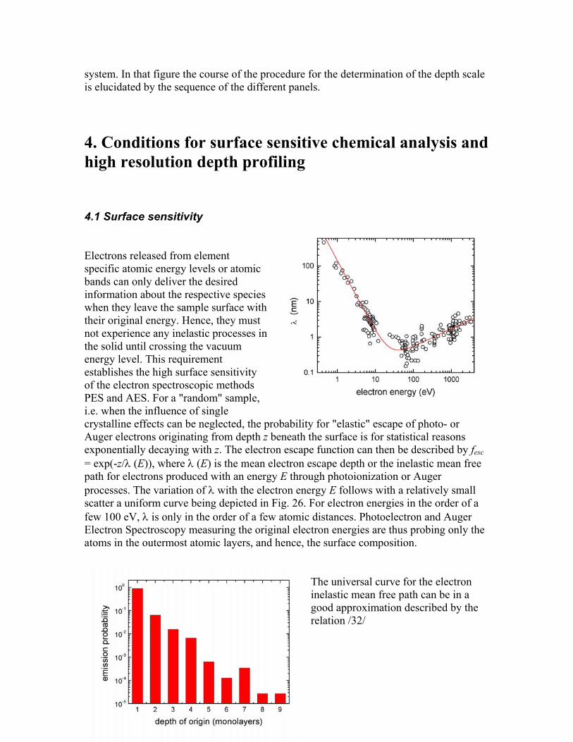
Electrons released from element specific atomic energy levels or atomic bands can only deliver the desired information about the respective species when they leave the sample surface with their original energy. Hence, they must not experience any inelastic processes in the solid until crossing the vacuum energy level. This requirement establishes the high surface sensitivity of the electron spectroscopic methods PES and AES. For a "random" sample, i.e. when the influence of single crystalline effects can be neglected, the probability for "elastic" escape of photo- or Auger electrons originating from depth z beneath the surface is for statistical reasons exponentially decaying with z. The electron escape function can then be described by fesc = exp(-z/λ (E)), where λ (E) is the mean electron escape depth or the inelastic mean free path for electrons produced with an energy E through photoionization or Auger processes. The variation of λ with the electron energy E follows with a relatively small scatter a uniform curve being depicted in Fig. 26. For electron energies in the order of a few 100 eV, λ is only in the order of a few atomic distances. Photoelectron and Auger Electron Spectroscopy measuring the original electron energies are thus probing only the atoms in the outermost atomic layers, and hence, the surface composition.
The universal curve for the electron inelastic mean free path can be in a good approximation described by the relation /32/

λ (E) = AE -2 + B (E)0.5 (14)
λ (E) is obtained in terms of nanometers when the electron energy E is given in eV. The coefficients A and B amount to 143 and 0.054 for elements or to 641 and 0.0.096 for inorganic compounds (cf. ref. , p. 209).
The information depth of the mass spectrometric techniques SNMS and SIMS is comparable with λ (E) or even more shallow. This can be demonstrated by computer simulations of the interaction of energetic particles with solid surfaces //. An example is given in Fig. 27, which shows the distribution of the depth of origin which was calculated for Ag atoms sputtered from a single crystalline (111) silver surface by impact of normally incident 5-keV Ar+ ions. The data were obtained from a so-called Molecular Dynamics Simulation, in which the classical equations of motion are solved numerically for all atoms of a model crystal consisting of 2300 atoms. It is seen that more than 90 % of the sputtered atoms originate from the uppermost atomic layer, the mean information depth calculated by fitting an exponential decay to the distribution amounts to approximately 0.5 atomic layers.
4.2 Experimental techniques for high resolution depth profiling
For relatively thick layer structures bevelling or tapered section techniques can be applied in order to obtain depth dependent chemical information across the layer thickness. Tapering can be achieved by appropriate machining as, for instance, the formation of a flat bowl with a rotating ball. Extremely flat bevelling angles down to 10-4 - 10-
5 degrees can also be realized by sputter erosion with an ion beam of slight divergence, i.e. a minute lateral variation of the ion current density.
The depth resolution achieved across a tapered section can be estimated from Fig. 28. When an ideally sharp interface between 2 sublayers or between a coating and the substrate is probed by an analyzing electron or ion beam of diameter db, the (absolute) depth resolution ∆z is given by /12/

∆ z = db sinα + δ l cosα , (15)
where α is the bevelling angle and δl is the information depth of the analytical technique (see sect. 4.1). ∆z becomes smallest when the influence of the larger of the two quantities db or δl is minimized via the choice of the bevelling angle α . Since in most cases the information depth δl is below the beam diameter db, a depth resolution ∆z close to the information depth is obtained for α→ 0. Therefore, bevelling angles well below 1° should be used when mechanically cutting through a thick layer structure.
It can be readily seen from equ. (15) that for small δ l a sample removal parallel to the film plane, i.e. with α = 0, is most favorable. In that case ion sputtering is the most appropriate microsectioning technique. However, special precautions are mandatory to eliminate deteriorating influences from so-called crater effects, i.e. from a curved bottom of the sputtering crater, or from signal contributions from the crater walls. Lateral inhomogeneities of the bombarding ion current density within the analyzed spot on the surface have, therefore, to be strictly avoided. This can be achieved by rastering a (high energy) ion beam across the analyzed area or by establishment of an extremely plane extraction geometry in the case of low energy ion bombardment from a low pressure plasma /34/. The latter method is used in the DBM-mode of electron gas SNMS (see section 3.2). The example shown in Fig. 27 has been obtained with this technique.
Signal contributions from the crater walls can be suppressed for AES when the narrow probing electron beam is directed preferentially to the center of the ion beam raster area, or for SIMS and SNMS when an appropriate gating technique ensures that signal recording is only performed when the raster-scanned ion beam hits the center of the sputter crater. In the direct bombardment mode of SNMS contributions from the crater walls are suppressed when the diameter of the bombarded area becomes large enough so that again only its central part is "seen" by the entrance aperture of the detection system.
Depth resolution in sputter profiling can further be deteriorated by a number of effects as the development of a bombardment induced surface micro-topography due to structural or chemical inhomogeneities of the sample /35/, by collisional atomic mixing effects which may smear out sharp interfaces in the analyzed film structure, and a delayed or preferred sputter removal of different sample constituents. The latter effect does not only result in a delayed signal decay when profiling across an interface, but is even more

important in view of the resulting variations of the surface composition due to preferential sputtering effects. As already mentioned in section 1, this may lead to strong differences in the analytical information obtained with electron spectroscopic techniques on one side and mass spectrometric methods on the other.
Optimum depth resolution is quite obviously achieved when atomic mixing effects are avoided, i.e. when energy deposition through the ion bombardment is confined to the information depth of the respective analytical method. Hence, a low energy and/or a high mass of the bombarding ions resulting in a very limited range of the impinging ions in the solid is most preferable. By SNMS depth profiling with normally incident Ar+-ions of only 200 eV, the experimental interface width between 2 sublayers in a Si/Ta-multilayer structure has been found to be in the order of only 1.5 nm /36/. This agrees well with the extrapolated values in Fig. 11 and, hence, the physical limit given by the atomic roughness arising from the statistics of the removal of surface atoms during the sputter process. From corresponding simulations such an atomic roughness is found to be in the order of 4 - 5 atomic distances which agrees well with the best interface widths obtained in sputter depth profiling.
References
1 D. Briggs, M.P. Seah, Practical Surface Analysis, Vol. 1: Auger and X-Ray Photoelectron Spectroscopy, 2nd Ed. (Chichester, New York: Wiley; Aarau, Frankfurt: Salle und Sauerländer 1990)
2 D. Briggs, M.P. Seah, Practical Surface Analysis, Vol. 2: Ion and Neutral Spectroscopy (Chichester, New York: Wiley; Aarau, Frankfurt: Salle und Sauerländer 1992)
3 H. Oechsner, Verfahren zur Untersuchung von Festkörperoberflächen, in Kohlrausch Praktische Physik, 24. Aufl. Bd. 2, p. 717-738 (Teubner, Stuttgart 1996)
4 L.C. Feldman, J.W. Mayer, Fundamentals of Surface and Thin Film Analysis (Elsevier, New York 1986)
5 H. Oechsner (ed.), Thin Film and Depth Profile Analysis (Topics in Current Physics Vol. 37, Springer, Berlin Heidelberg 1984)
6 J. Bartella, H. Hoffmann, K.H. Müller, G. Reiss, Moderne Verfahren der Oberflächen- und Dünnschichtanalyse, in G. Kienel (Hrsg.), Vakuumbeschichtung Bd 3 (VDI-Verlag, Düsseldorf 1994) p. 248-335
7 H. Bach, F.G.K. Baucke, Investgation of Glasses Using Surface Profiling by Spectrochemical Analysis of Sputter-Induced Radiation, J. Amer. Ceram. Soc. 65 (1982), 527-539
8 W.K. Chu, J.W. Mayer, M.A. Nicolet, Backscattering Spectrometry (Academic Press, New York, San Francisco, London 1978)

9 B.K. Teo, D.C. Joy (eds.), EXAFS Spectroscopy (Plenum Press, London 1981)
10 H. Aiginger, Historical Development and Principles of Total Reflection X-ray Fluorescence Analysis (TXRF), Spectrochimica Acta 46B (1991), 1313 and references therein
11 H.J. Güntherodt, R. Wiesendanger (eds.), Scanning Tunneling Microscopy I and II (Springer Ser. Surface Sci. Vol. 20 and Vol. 28, Springer Berlin 1992)
12 H. Oechsner, Recent Progress in High Resolution Depth Profiling and Interface Analysis of Thin Films, Vacuum 37 (1987), 763-768
13 Handbook of X-ray Photoelectron Spectroscopy, J. Chastain, ed. (Physical Electronics, Eden Prairie 1992)
14 Handbook of Auger Electron Spectroscopy, 3rd Ed., C.L. Hedberg, ed. (Physical Electronics, Eden Prairie 1995)
15 H. Oechsner, Scanning Auger Microscopy, Le Vide, les Couches Minces 271 (1994), 141-150
16 H. Oechsner, Surface and Depth Profile Analysis of Insulator Materials, Proc. 5th SURTEC, Berlin 1989 (Hanser Verlag München), 485-492
17 H. Schoof, Untersuchung an anodischen Tantal- und Nioboxidschichten mit AES und SNMS, PhD Dissertation, TU Clausthal 1981
18 A. Zalar, Improved Depth Resolution by Sample Rotation during Auger Electron Spectroscopy Depth Profiling, Thin Solid Films 124 (1985), 223-230
19 A. Wucher, Energieverteilungen und spektrale Ionisierungswahrscheinlichkeiten bei der beschußinduzierten Teilchenemission aus oxidierten Metalloberflächen, PhD Thesis, University of Kaiserslautern, 1996
20 H. Gnaser, H. Oechsner, The Influence of Polarizability on the Emission of Sputtered Molecular Ions, Surf. Sci. Lett. 302 (1994), L289-L292
21 H. Gnaser, Improved quantification in secondary-ion mass spectrometry detecting MCs+ molecular ions, J. Vac. Sci. Technol. A12 (1994), 452-456
22 A. Wucher, Microanalysis of Solid Surfaces by Secondary Neutral Mass Spectrometry, Fresenius J. Anal. Chem. 346 (1993), 3-10
23 H. Oechsner, Secondary Neutral Mass Spectrometry (SNMS) - Recent Methodical Progress and Applications to Fundamental Studies in Particle/Surface Interaction, Int. J. Mass. Spectrom. Ion Processes 143 (1995), 271-282
24 H. Oechsner, Analysis of Insulator Samples by Secondary Neutral Mass Spectrometry, Scanning Microscopy 3 (1989), 411-418
25 W. Bieck, H. Gnaser, H. Oechsner, Analytical Performance of a Secondary-Neutral Microprobe with Electron-gas Postionization and Magnetic-Sector Mass Spectrometer, J Vac. Sci. Technol. A12 (1994), 2537-2543

26 D. Lipinsky, R. Jede, H. Tümpner, O. Ganschow, A. Benninghoven, High Sensitivity Quasisimultaneous Secondary Neutral, Secondary Ion and Residual Gas Mass Spectrometry by a new Electron Impact Postionizer, J. Vac. Sci. Technol. A3 (1985), 2035-
27 U. Breuer, H. Holzbrecher, M. Gastel, J.S. Becker, H.-J. Dietze, Comparative Studies of MCs+-SIMS and e--beam SNMS for Quantitative Analysis of Bulk Materials and Layered Structures, Fres. J. Anal. Chem. 353 (1995), 372-377
28 C.S. Hansen, W.F. Calaway, M.J. Pellin, R.C. Wiens, D.S. Burnett, Three-Color Resonance Ionization spectroscopy of Zr in Si, Resonance Ionization Spectroscopy 1996, ed. N. Winograd, J.E. Parks, AIP Conference Proceedings 388 (AIP Press, Woodbury, 1997), p. 215-218
29 M. Wulff, A. Wucher, Quantitation of Single Photon Ionization Laser-SNMS, Secondary Ion Mass Spectrometry SIMS XI, ed. G. Gillen, R. Lareau, J. Bennet, F. Stevie (Whiley, New York 1998), 665-668
30 W. Berthold, A. Wucher, Laterally Resolved Chemical Analysis of Solid Surfaces by Laser-SNMS, Surf. Interf. Anal. 23 (1995), 393-398
31 A. Wucher and H. Oechsner, Depth Scale Calibration during Sputter Removal of Multilayer Systems by SNMS, Fresenius Z. Anal. Chem. 333 (1989), 470-473
32 M.P. Seah, W.A. Dench, Quantitative Electron Spectroscopy of Surfaces: Standard Data Base for Electron Inelastic Mean Free Path in Solids, Surf. Interf. Anal. 1 (1979), 2-11
33 A. Wucher, B.J. Garrison, Cluster Formation in Sputtering: A Molecular Dynamics Study using the MD/MC-Corrected Effective Medium Potential, J. Chem. Phys. 105 (1996), 5999-6007
34 E. Stumpe, H. Oechsner, H. Schoof, High Resolution Sputter Depth Profiling with a Low Pressure HF-Plasma, Appl. Phys. 20 (1979), 55-60
35 D. Grunenberg, D. Sommer, K.H. Koch, Examinations Regarding the Correctness of Quantitative Surface Analysis Using SNMS, Fresenius J. Anal. Chem. 346 (1993), 147-150
36 H. Oechsner, Recent Applications of Secondary Neutral Mass Spectrometry for Quantitative Analysis of Homogeneous and Structured Samples, Nucl. Inst. & Meth. in Phys. Res. B33 (1988), 918-925