scanning electron microscopic characterization of copper ... · scanning electron microscopic...
TRANSCRIPT
Scanning Electron Microscopic Characterization of Copper (II) Phthalocyanine Nanocrystallites Thin Films Deposited on Technologically Important Substrates
Biswanath Mallik* and Santanu Karan Department of Spectroscopy, Indian Association for the Cultivation of Science, 2A & 2B, Raja S. C.
Mullick Road, Jadavpur, Kolkata-700 032, India. Field Emission Scanning Electron Microscopy (FESEM) demonstrates spectacular changes in the morphology of thin films of copper (II) phthalocyanine (CuPc) deposited on gold coated quartz substrates at different substrate temperatures, and on indium tin oxide (ITO) substrates at room temperature followed by post deposition annealing at various temperatures under normal atmosphere. The nature of substrates, the film deposition as well as annealing temperature play an important role in the molecular organization of CuPc molecules on the substrates resulting in nanoparticles, nanoflowers, nanocabbages, nanoribbons, nanorods etc. The single crystalline nature of the CuPc nanoribbon has been indicated from the SAED pattern obtained from Transmission Electron Microscope (TEM). The long nanoribbons of β-phase CuPc grow along the stacking axis of the CuPc molecules. Using the FESEM images, the fractal dimension of the assembly of nanostructures in the films has been estimated. The effects of substrates, substrate temperature, and annealing temperature on the surface morphology and fractal dimension have been discussed.
Keywords Copper (II) phthalocyanine, Gold and ITO substrates, Thin films, Nanostructures, Morphology, Fractal dimension.
1. Introduction
Metal phthalocyanines (MPcs) are very well known dye pigments having similarity in structure with biological molecules chlorophyll and hemoglobin. They exist as a range of derivatives, where the polyaromatic ring (abbreviated Pc for the phthalocyanato anion C32 H16N8
2- ) is most commonly bound to a transition metal (MPc) or hydrogen (H2Pc) [1]. These materials have shown many interesting properties, e.g., these are organic semiconductors [2,3], chemically and thermally very stable [4,5], most of these can easily form ordered thin films and exhibit photoconductivity [6,7]; show catalytic activity [8] etc. A great deal of attention has been paid for a wide variety of applications of MPcs, such as dyes [9], light emitting diodes (LEDs)[10], solar cells [6,7] and field-effect transistors [11]. Attempts have been made to use MPc films as molecular components in a number of electronic and optoelectronic devices [6,7,12]. It has been reported that the structure, morphology, electronic and optical properties of the films are crucial for their technological applications [13] and the ordering and orientation of the molecules are very important factor for the device efficiency [13]. An understanding of the molecular orientation, electronic structure and morphology of thin film systems is a prerequisite for being able to tune their electronic as well as optoelectronic properties. The molecular orientation and electronic structure of MPcs have been investigated experimentally, in various forms and on different substrates such as conducting polymer [14], silicon [15], gold [16-18] etc., as well as theoretically [19-21]. Such studies have indicated that the orientation of the grains depends on the nature of the substrate, the deposition technique, heat-treatment temperatures and conditions of the substrates during film deposition.
* Corresponding author: e-mail: [email protected], Phone: +91-33-2473-4971; Fax: + 91-33-2473-2805
Modern Research and Educational Topics in Microscopy. A. Méndez-Vilas and J. Díaz (Eds.) ©FORMATEX 2007
671
_______________________________________________________________________________________________
As an example, copper (II) phthalocyanine (CuPc) was reported to lie flat on the Au (100) surface, but to stand upright on the polycrystalline surface [22,23] while deposited under identical conditions. Tong et al [24] have grown nanoribbons and nanowires of different MPcs by the method of organic vapour-phase deposition. Tang et al [25] using vapour deposition technique reported the sub micrometer size ribbon of copper phthalocyanine on porous aluminium oxide substrate. Among a number of different MPcs, CuPc has been most extensively studied [7,22,23,25-32]. Such studies include the use of CuPc as solar cells [7], color sensor [26], electroluninescent device [27], interfacial properties [22,29-31] etc. Many electronic and optoelectronic devices rely on the growth of molecular thin films structures on metal electrodes. In our laboratory, attempts were made to study the interactions of CuPc with various technologically important electrode materials like gold and indium tin oxide (ITO). Recently we have reported the surface morphology of CuPc molecules deposited at room temperature (30 oC) on polycrystalline gold substrates and the formation of CuPc nanoparticles and nanoflowers [33]. Film deposition on suitable gold substrates at higher substrate temperatures has shown CuPc structures like nanocabbages, nanoribbons etc [34]. Such studies have indicated that the morphology of the CuPc films depends on the substrate, heat-treatment temperatures and condition of substrates during film deposition. CuPc films deposited on ITO at room temperature under post-deposition annealing have shown significant changes in film morphology. The fractal dimension of the assembly of nanostructures in the films was estimated from the FESEM images. The effects of substrates and substrate temperature on the surface morphology and the fractal dimension were studied extensively. These aspects are discussed in this chapter and these are based on the results reported elsewhere [33,34].
2. Experimental Section
Gold single crystal with (111) surface orientation was used as a target. Clean gold surfaces were prepared on the surface of clean quartz plates by D.C. sputtering (7 KV, 10 mA) for 4 min followed by annealing for 1h at 500 and 750 0C under vacuum. The substrates annealed at 500 0C and 750 0C are referred as Au-500 and Au-750, respectively. Clean ITO coated glass plates were also used as substrates. The CuPc source powder (in β form, dye content ~97%, obtained from Aldrich, U.S.A.; molecular structure is shown in figure 1) contained in a molybdenum boat was resistively heated in the high vacuum chamber. The source CuPc powder was used after repeated degassing of the source prior to deposition.
Deposition was noted to occur when the chamber pressure could no longer reduce to the base pressure and the current through the boat was kept constant. All CuPc films were deposited at a chamber pressure of ~10-6 Torr. The thickness of the deposited CuPc films and the rate of deposition were maintained at 100 nm and 0.6 Ǻ/sec, respectively using a quartz crystal microbalance (Hitech, model DTM-101). The temperature of the substrates during deposition of CuPc on quartz plate, Au-500 and Au-750 was adjusted in the range of 30 to 280 oC using a high precision temperature controller (Eurotherm 2404,
Fig. 1 Molecular structure of CuPc
©FORMATEX 2007Modern Research and Educational Topics in Microscopy. A. Méndez-Vilas and J. Díaz (Eds.)
672
_______________________________________________________________________________________________
UK). The CuPc films on ITO were deposited at a substrate temperature of 30 oC (room temperature). After deposition of CuPc film on ITO, the films were annealed for 1 h at different temperatures ranging from 30 to 310 oC under normal atmosphere (similar technique as used by Jungyoon et. al [35]). The thin films were characterized by optical absorption (not shown), X-ray diffraction (XRD), Field Emission Scanning Electron Microscopy (FESEM) and Transmission Electron Microscopy (TEM). XRD study of the CuPc films deposited at different substrate temperatures were recorded at a scan rate of 0.05o per sec by using a Seifert XRD 3000P Difractrometer with Cu-Kα radiation (0.15418 nm). UV-Vis. Scanning Spectrophotometer (UV-2401 PC, Shimadzu, Japan) was used to record the electronic absorption spectra of the films at room temperature. FESEM (Model: JSM-6700F, JEOL, Japan) was used to record the scanning electron micrograph images of the CuPc thin films. The collected sample from a thin film was dispersed in water and cast on carbon coated copper grid and dried in vacuum for overnight. The images were then taken by a Transmission Electron Microscope (TEM) (Model: JEM-2010, JEOL, Japan). To estimate the surface roughness of the thin films, the contact mode Atomic Force Microscopy (AFM) images were taken using NT-MDT (Solver PRO-M), Moscow, Russia.
3. Results and discussion
3.1. Preparation of gold template
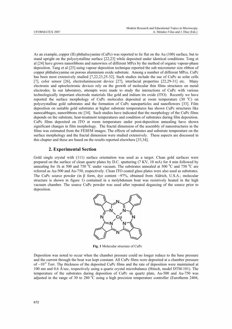
The FESEM images of the gold thin films are shown in figure 2(a) and (b). The FESEM image in figure 2(a) shows the morphology of the annealed (at 500 0C) gold thin film (Au-500). Clearly there are some islands (300-500 nm) of gold nanoparticles and some pores (150-200 nm), which are distributed in random order, but the distribution of the islands and pores are almost same throughout the whole film. Inset of Figure 2 (a) shows the FESEM image of as prepared gold nanoparticles on quartz.
(a) (b)
(c) (d)
Fig. 2 FESEM images of sputtered gold nanoparticles: (a) thin film morphology of Au-500 showing island and pores, inset shows the pattern for as deposited gold on quartz; (b) spherical and elliptical clusters of different sizes of gold in Au-750, inset shows one large spherical gold cluster. Panels (c) and (d) show the contact mode 3-D AFM image of gold substrates Au-500 and Au-750, respectively.
Modern Research and Educational Topics in Microscopy. A. Méndez-Vilas and J. Díaz (Eds.) ©FORMATEX 2007
673
_______________________________________________________________________________________________
The gold nanoparticles are almost spherical in shape and the average size is around 30 nm. The FESEM image in figure 2(b) shows the morphology of the gold thin film annealed at 750 0C (Au-750). Here, bigger particles of some spherical and elliptical shapes and with different sizes ranging from 100 nm to 500 nm are seen. The inset of figure 2(b) represents one such spherical nanoparticle of size nearly 320 nm surrounded by nano-sized particles with sizes from 10 to 20 nm at higher magnification. Panels c and d represent the contact mode three dimensional (3-D) AFM images for Au-500 and Au-750 surfaces, respectively. The calculated rms roughness of Au-500 is 2.1 nm and that of Au-750 is 85.0 nm which indicates that roughness of Au-750 is significantly higher than that of Au-500 substrate.
3.2. CuPc thin films deposited on various substrates at different temperatures and FESEM images
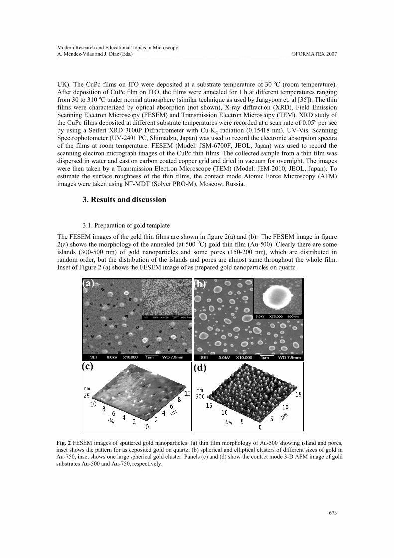
Figure 3 shows the FESEM images of CuPc thin films deposited on various substrates at room temperature (30 0C). The image of CuPc thin film deposited on bare quartz is shown in figure 3(a), which shows clearly almost uniform distribution of some nano-sized particles of size around 25 to 30 nm. From figure 3(b), dense and aggregated packing of CuPc nanoparticles are found to be deposited on Au-500 substrate at room temperature with average particle size estimated to be nearly 40 to 60 nm. FESEM image of CuPc deposited on substrate Au-750 at room temperature, as demonstrated in figure 3(c), shows some flower like structures with different shapes and sizes ranging from 200 nm to 1 µm. The residual position on the film has been found to be uniformly covered by the nanoparticles. Figure 3(d)
shows one such nanoflower of size (diameter) around 900 nm in a magnified scale. The flower consists of some nanorods of CuPc of diameter nearly 25 nm and of length varying from few nanometers to higher values. The structures of such nanoflowers arise due to the interaction of CuPc molecules with annealed gold template (Au-750) having spherical and elliptical particles of various sizes ranging from few nanometer to micrometer. The initial nucleation of CuPc molecules occurs at room substrate temperature on the gold template and form flower like structure through the process of self-organization. FESEM images of CuPc thin films deposited at 85 0C substrate temperature are shown in figure 4. The
(c)
(b) (a)
(d) (d) (c)
(a) (b)
Fig. 4 FESEM images of vacuum deposited CuPc thin films at 85 0C: (a) CuPc nanoribbons deposited on quartz; (b) aggregated CuPc nanoparticles deposited on Au-500; (c) CuPc nanocabbages deposited on Au-750 and (f) CuPc nanocabbage at higher magnification.
Fig. 3 FESEM images of vacuum deposited CuPc thin films at room temperature: (a) CuPc nanoparticles deposited on quartz; (b) dense and aggregated CuPc nanoparticles deposited on Au-500; (c) spherical and elliptical CuPc nanoflowers deposited on Au-750 and (d) CuPc nanoflower at higher magnification.
©FORMATEX 2007Modern Research and Educational Topics in Microscopy. A. Méndez-Vilas and J. Díaz (Eds.)
674
_______________________________________________________________________________________________
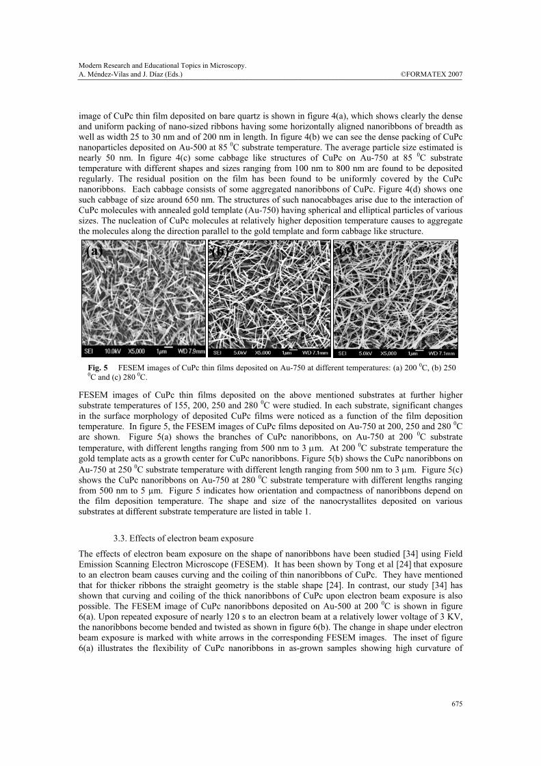
image of CuPc thin film deposited on bare quartz is shown in figure 4(a), which shows clearly the dense and uniform packing of nano-sized ribbons having some horizontally aligned nanoribbons of breadth as well as width 25 to 30 nm and of 200 nm in length. In figure 4(b) we can see the dense packing of CuPc nanoparticles deposited on Au-500 at 85 0C substrate temperature. The average particle size estimated is nearly 50 nm. In figure 4(c) some cabbage like structures of CuPc on Au-750 at 85 0C substrate temperature with different shapes and sizes ranging from 100 nm to 800 nm are found to be deposited regularly. The residual position on the film has been found to be uniformly covered by the CuPc nanoribbons. Each cabbage consists of some aggregated nanoribbons of CuPc. Figure 4(d) shows one such cabbage of size around 650 nm. The structures of such nanocabbages arise due to the interaction of CuPc molecules with annealed gold template (Au-750) having spherical and elliptical particles of various sizes. The nucleation of CuPc molecules at relatively higher deposition temperature causes to aggregate the molecules along the direction parallel to the gold template and form cabbage like structure.
FESEM images of CuPc thin films deposited on the above mentioned substrates at further higher substrate temperatures of 155, 200, 250 and 280 0C were studied. In each substrate, significant changes in the surface morphology of deposited CuPc films were noticed as a function of the film deposition temperature. In figure 5, the FESEM images of CuPc films deposited on Au-750 at 200, 250 and 280 0C are shown. Figure 5(a) shows the branches of CuPc nanoribbons, on Au-750 at 200 0C substrate temperature, with different lengths ranging from 500 nm to 3 µm. At 200 0C substrate temperature the gold template acts as a growth center for CuPc nanoribbons. Figure 5(b) shows the CuPc nanoribbons on Au-750 at 250 0C substrate temperature with different length ranging from 500 nm to 3 µm. Figure 5(c) shows the CuPc nanoribbons on Au-750 at 280 0C substrate temperature with different lengths ranging from 500 nm to 5 µm. Figure 5 indicates how orientation and compactness of nanoribbons depend on the film deposition temperature. The shape and size of the nanocrystallites deposited on various substrates at different substrate temperature are listed in table 1.
3.3. Effects of electron beam exposure
The effects of electron beam exposure on the shape of nanoribbons have been studied [34] using Field Emission Scanning Electron Microscope (FESEM). It has been shown by Tong et al [24] that exposure to an electron beam causes curving and the coiling of thin nanoribbons of CuPc. They have mentioned that for thicker ribbons the straight geometry is the stable shape [24]. In contrast, our study [34] has shown that curving and coiling of the thick nanoribbons of CuPc upon electron beam exposure is also possible. The FESEM image of CuPc nanoribbons deposited on Au-500 at 200 0C is shown in figure 6(a). Upon repeated exposure of nearly 120 s to an electron beam at a relatively lower voltage of 3 KV, the nanoribbons become bended and twisted as shown in figure 6(b). The change in shape under electron beam exposure is marked with white arrows in the corresponding FESEM images. The inset of figure 6(a) illustrates the flexibility of CuPc nanoribbons in as-grown samples showing high curvature of
Fig. 5 FESEM images of CuPc thin films deposited on Au-750 at different temperatures: (a) 200 0C, (b) 250 0C and (c) 280 0C.
(a) (b) (c)
Modern Research and Educational Topics in Microscopy. A. Méndez-Vilas and J. Díaz (Eds.) ©FORMATEX 2007
675
_______________________________________________________________________________________________
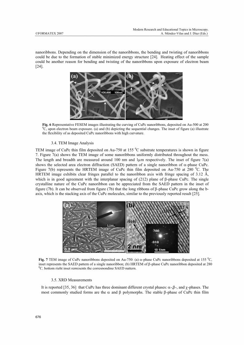
nanoribbons. Depending on the dimension of the nanoribbons, the bending and twisting of nanoribbons could be due to the formation of stable minimized energy structure [24]. Heating effect of the sample could be another reason for bending and twisting of the nanoribbons upon exposure of electron beam [24].
3.4. TEM Image Analysis
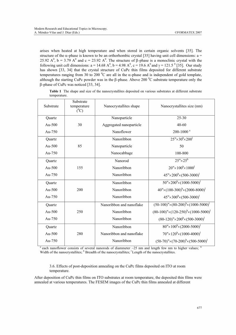
TEM image of CuPc thin film deposited on Au-750 at 155 0C substrate temperatures is shown in figure 7. Figure 7(a) shows the TEM image of some nanoribbons uniformly distributed throughout the mess. The length and breadth are measured around 100 nm and 1µm respectively. The inset of figure 7(a) shows the selected area electron diffraction (SAED) pattern of a single nanoribbon of α-phase CuPc. Figure 7(b) represents the HRTEM image of CuPc thin film deposited on Au-750 at 280 0C. The HRTEM image exhibits clear fringes parallel to the nanoribbon axis with fringe spacing of 3.12 Ǻ, which is in good agreement with the interplanar spacing of (212) plane of β-phase CuPc. The single crystalline nature of the CuPc nanoribbon can be appreciated from the SAED pattern in the inset of figure (7b). It can be observed from figure (7b) that the long ribbons of β-phase CuPc grow along the b-axis, which is the stacking axis of the CuPc molecules, similar to the previously reported result [25].
3.5. XRD Measurements
It is reported [35, 36] that CuPc has three dominant different crystal phases: α-,β-, and χ-phases. The most commonly studied forms are the α and β polymorphs. The stable β-phase of CuPc thin film
(a)
200
010
3.12 Ǻ (212)
(010)
(b)
Fig. 7 TEM image of CuPc nanoribbons deposited on Au-750: (a) α-phase CuPc nanoribbons deposited at 155 0C, inset represents the SAED pattern of a single nanoribbon; (b) HRTEM of β-phase CuPc nanoribbon deposited at 280 0C, bottom right inset represents the corresponding SAED pattern.
(b)(a)
Fig. 6 Representative FESEM images illustrating the curving of CuPc nanoribbons, deposited on Au-500 at 200 0C, upon electron beam exposure. (a) and (b) depicting the sequential changes. The inset of figure (a) illustrate the flexibility of as deposited CuPc nanoribbons with high curvature.
©FORMATEX 2007Modern Research and Educational Topics in Microscopy. A. Méndez-Vilas and J. Díaz (Eds.)
676
_______________________________________________________________________________________________
arises when heated at high temperature and when stored in certain organic solvents [35]. The structure of the α-phase is known to be an orthorhombic crystal [35] having unit cell dimensions: a = 25.92 A0, b = 3.79 A0 and c = 23.92 A0. The structure of β-phase is a monoclinic crystal with the following unit cell dimensions: a = 14.68 A0, b = 4.98 A0, c = 19.6 A0 and γ = 121.5 0 [35]. Our study has shown [33, 34] that the crystal structure of CuPc thin films deposited for different substrate temperatures ranging from 30 to 200 0C are all in the α-phase and is independent of gold template, although the starting CuPc powder was in the β-phase. Above 200 0C substrate temperature only the β-phase of CuPc was noticed [33, 34].
Table 1 The shape and size of the nanocrystallites deposited on various substrates at different substrate temperature.
Substrate Substrate
temperature (0C)
Nanocrystallites shape Nanocrystallites size (nm)
Quartz
Au-500
Au-750
30
Nanoparticle
Aggregated nanoparticle
Nanoflower
25-30
40-60
200-1000 a
Quartz
Au-500
Au-750
85
Nanoribbon
Nanoparticle
Nanocabbage
25w×30b×200l
50
100-800
Quartz
Au-500
Au-750
155
Nanorod
Nanoribbon
Nanoribbon
25w×25b
20w×100b×1000l
45w×200b×(500-3000)l
Quartz
Au-500
Au-750
200
Nanoribbon
Nanoribbon
Nanoribbon
50w×200b×(1000-5000)l
40w×(100-300)b×(2000-8000)l
45w×300b×(500-3000)l
Quartz
Au-500
Au-750
250
Nanoribbon and nanoflake
Nanoribbon
Nanoribbon
(50-100)w×(80-200)b×(1000-5000)l
(80-100)w×(120-250)b×(1000-5000)l
(80-120)w×200b×(500-3000)l
Quartz
Au-500
Au-750
280
Nanoribbon
Nanoribbon and nanoflake
Nanoribbon
80w×100b×(2000-5000)l
70w×120b×(1000-4000)l
(50-70)w×(70-200)b×(500-5000)l a each nanoflower consists of several nanorods of diammeter ~25 nm and length few nm to higher values; w Width of the nanocrystallites; b Breadth of the nanocrystallites; l Length of the nanocrystallites.
3.6. Effects of post-deposition annealing on the CuPc films deposited on ITO at room temperature.
After deposition of CuPc thin films on ITO substrates at room temperature, the deposited thin films were annealed at various temperatures. The FESEM images of the CuPc thin films annealed at different
Modern Research and Educational Topics in Microscopy. A. Méndez-Vilas and J. Díaz (Eds.) ©FORMATEX 2007
677
_______________________________________________________________________________________________
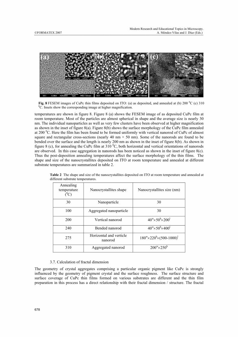
temperatures are shown in figure 8. Figure 8 (a) shows the FESEM image of as deposited CuPc film at room temperature. Most of the particles are almost spherical in shape and the average size is nearly 30 nm. The individual nanoparticles as well as very few clusters have been observed at higher magnification as shown in the inset of figure 8(a). Figure 8(b) shows the surface morphology of the CuPc film annealed at 200 0C. Here the film has been found to be formed uniformly with vertical nanorod of CuPc of almost square and rectangular cross-sections (nearly 40 nm × 50 nm). Some of the nanorods are found to be bended over the surface and the length is nearly 200 nm as shown in the inset of figure 8(b). As shown in figure 8 (c), for annealing the CuPc film at 310 0C, both horizontal and vertical orientations of nanorods are observed. In this case aggregation in nanorods has been noticed as shown in the inset of figure 8(c). Thus the post-deposition annealing temperatures affect the surface morphology of the thin films. The shape and size of the nanocrystallites deposited on ITO at room temperature and annealed at different substrate temperatures are summarized in table 2.
Table 2 The shape and size of the nanocrystallites deposited on ITO at room temperature and annealed at different substrate temperatures.
Annealing temperature
(0C) Nanocrystallites shape Nanocrystallites size (nm)
30 Nanoparticle 30
100 Aggregated nanoparticle 30
200 Vertical nanorod 40w×50b×200l
240 Bended nanorod 40w×50b×400l
275 Horizontal and verticle nanorod 180w×220b×(500-1000)l
310 Aggregated nanorod 200w×250b
3.7. Calculation of fractal dimension
The geometry of crystal aggregates comprising a particular organic pigment like CuPc is strongly influenced by the geometry of pigment crystal and the surface roughness. The surface structure and surface coverage of CuPc thin films formed on various substrates are different and the thin film preparation in this process has a direct relationship with their fractal dimension / structure. The fractal
(a)
(b)
(c)
Fig. 8 FESEM images of CuPc thin films deposited on ITO: (a) as deposited, and annealed at (b) 200 0C (c) 310 0C. Insets show the corresponding image at higher magnification.
©FORMATEX 2007Modern Research and Educational Topics in Microscopy. A. Méndez-Vilas and J. Díaz (Eds.)
678
_______________________________________________________________________________________________
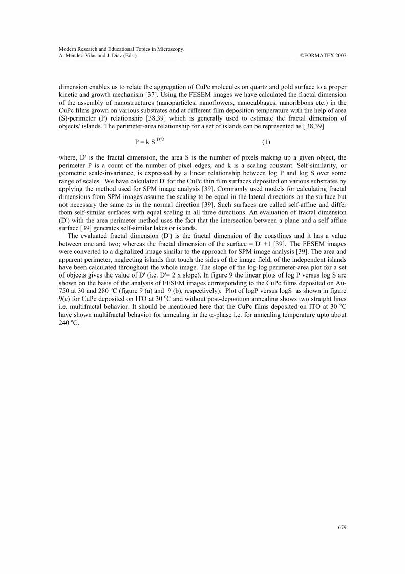
dimension enables us to relate the aggregation of CuPc molecules on quartz and gold surface to a proper kinetic and growth mechanism [37]. Using the FESEM images we have calculated the fractal dimension of the assembly of nanostructures (nanoparticles, nanoflowers, nanocabbages, nanoribbons etc.) in the CuPc films grown on various substrates and at different film deposition temperature with the help of area (S)-perimeter (P) relationship [38,39] which is generally used to estimate the fractal dimension of objects/ islands. The perimeter-area relationship for a set of islands can be represented as [ 38,39]
P = k S D'/2 (1) where, D' is the fractal dimension, the area S is the number of pixels making up a given object, the perimeter P is a count of the number of pixel edges, and k is a scaling constant. Self-similarity, or geometric scale-invariance, is expressed by a linear relationship between log P and log S over some range of scales. We have calculated D' for the CuPc thin film surfaces deposited on various substrates by applying the method used for SPM image analysis [39]. Commonly used models for calculating fractal dimensions from SPM images assume the scaling to be equal in the lateral directions on the surface but not necessary the same as in the normal direction [39]. Such surfaces are called self-affine and differ from self-similar surfaces with equal scaling in all three directions. An evaluation of fractal dimension (D') with the area perimeter method uses the fact that the intersection between a plane and a self-affine surface [39] generates self-similar lakes or islands. The evaluated fractal dimension (D') is the fractal dimension of the coastlines and it has a value between one and two; whereas the fractal dimension of the surface = D' +1 [39]. The FESEM images were converted to a digitalized image similar to the approach for SPM image analysis [39]. The area and apparent perimeter, neglecting islands that touch the sides of the image field, of the independent islands have been calculated throughout the whole image. The slope of the log-log perimeter-area plot for a set of objects gives the value of D' (i.e. D'= 2 x slope). In figure 9 the linear plots of log P versus log S are shown on the basis of the analysis of FESEM images corresponding to the CuPc films deposited on Au-750 at 30 and 280 oC (figure 9 (a) and 9 (b), respectively). Plot of logP versus logS as shown in figure 9(c) for CuPc deposited on ITO at 30 oC and without post-deposition annealing shows two straight lines i.e. multifractal behavior. It should be mentioned here that the CuPc films deposited on ITO at 30 oC have shown multifractal behavior for annealing in the α-phase i.e. for annealing temperature upto about 240 oC.
Modern Research and Educational Topics in Microscopy. A. Méndez-Vilas and J. Díaz (Eds.) ©FORMATEX 2007
679
_______________________________________________________________________________________________
Two values of fractal dimension indicate the presence of two distinct types of nanoparticles or nanorods or both in relation to their shape, size, orientation etc. However, at annealing temperatures 275 and 310 oC CuPc has shown β-phase and in this phase only one fractal dimension has been noticed as demonstrated in figure 9(d)) for a CuPc film on ITO annealed at 310 oC. The values of D' estimated in
Fig. 9 Variation of Log(P) with Log(S) derived from FESEM images for CuPc thin films deposited: on Au-750 at (a) 30 0C and (b) 280 0C; on ITO at 30 0C and without annealing (c) as well as annealed at 310 0C (d).
-14 -12 -10 -8 -6 -4-16
-14
-12
-10
-8
-6
D'=1.93
Log
(P)
Log (S)-14 -12 -10 -8 -6 -4
-16
-14
-12
-10
-8
-6
D'=1.63
D'=1.94
Log
(P)
Log (S)
-14 -12 -10 -8 -6 -4 -2-16
-14
-12
-10
-8
-6
-4
D'=1.76
Log
(P)
Log (S)-14 -12 -10 -8 -6 -4 -2
-16
-14
-12
-10
-8
-6
-4
D'=1.83
Log (S)
Log
(P)
(a) (b)
(c) (d)
Fig. 10 Variation of (a) fractal dimension and (b) Devydov splitting with substrate temperature for the CuPc thin films deposited on quartz, Au-500 and Au-750 respectively. (c) Variation of Devydov splitting (curve-1) and direct energy gap (curve-2) with the annealing temperature for the CuPc thin films deposited on ITO.
35 70 105 140 175 210 245 280
1.76
1.80
1.84
1.88
1.92
1.96
1
2
3
Frac
tal d
imen
sion
(D')
Substrate temperature ( 0C)
3 Au7502 Au5001 Quartz
50 100 150 200 250 3001.60
1.65
1.70
1.75
1.80
1.85
1.90
1.95
2.00
2
1
Frac
tal d
imen
sion
(D')
Annealing temperature ( 0C)
(a) (b)
©FORMATEX 2007Modern Research and Educational Topics in Microscopy. A. Méndez-Vilas and J. Díaz (Eds.)
680
_______________________________________________________________________________________________
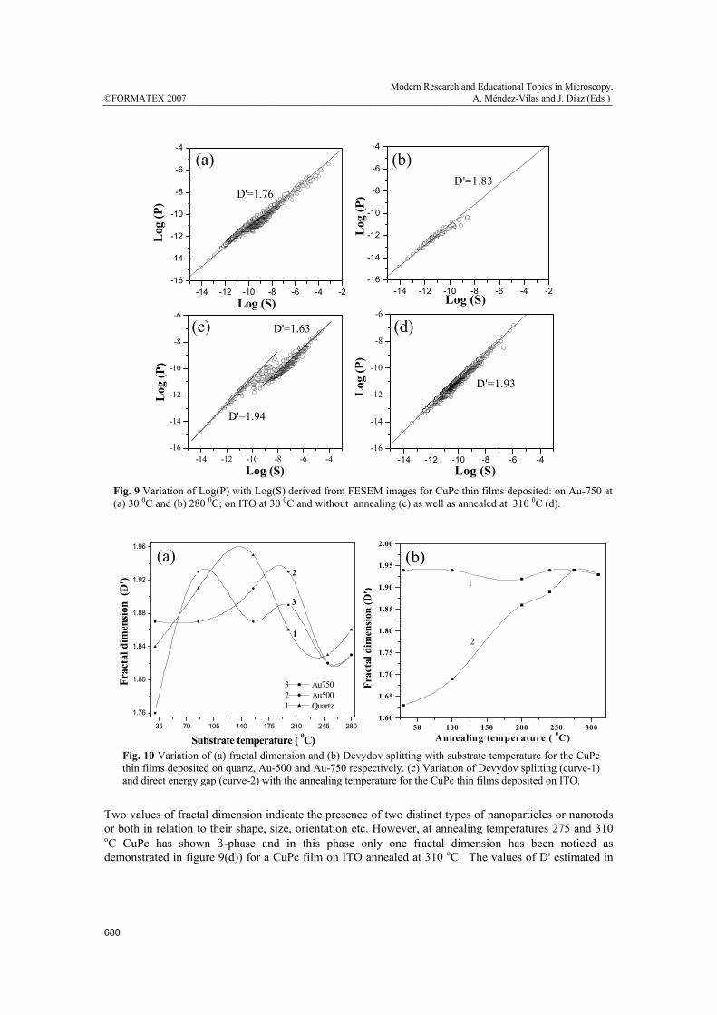
the present experiment agree with the fractal dimension estimated by Mather [40] for aggregated β-copper phthalocyanine pigment crystal (less than 2). Present study indicates that crystal aggregation depends on the nature of substrate, surface roughness, film deposition temperature as well as post-deposition annealing temperature. The variation of fractal dimension (D') with temperature of film deposition on quartz, Au-500 and Au-750 is shown in figure 10 (a). The fractal dimension (D') for all the substrates increases initially with the increase of film deposition temperature and at higher temperatures (α-phase to β-phase transition) it decreases and shows fluctuations/oscillations. In the present experiment, a fluctuation in fractal dimension noted at various temperatures for the thin films deposited on different substrates is possibly related to the phenomenon of phase transition [41-43]. Also the calculated fractal dimension is strongly dependent on the surface morphology of the films. Figure 10 (b) shows the variation of fractal dimension with annealing temperature in the case of ITO substrate. At lower temperature two values of fractal dimension are noticed and the difference between these values decreases with increase of post-deposition annealing temperature. At the β-phase of CuPc the two values of fractal dimension become equal i.e. one value is obtained.
4. Conclusions
For the growth of CuPc layer by vacuum evaporation, the surface morphology of the thin film is influenced very strongly by the nature of the gold template and the substrate temperature during film deposition. The crystal structures in all cases are independent of the growth conditions used to deposit the CuPc layer. The fractal dimension depends on the nature of substrate used and the film deposition temperature. Also for the growth of CuPc films on ITO by vacuum evaporation, the fractal dimension and surface morphology of the thin films are influenced very strongly on the post-deposition annealing temperature. In the α-phase, the CuPc films deposited on ITO have shown two values of fractal dimension i.e. multifractal behaviour but in the β-phase CuPc films have shown single fractal dimension in all the substrates used. The templating effects and the results regarding effects of annealing temperature on CuPc films deposited on ITO can be extended to structures involving the growth of multilayer heterostructures. The gold template as well as ITO can be useful as electrodes in optoelectronic devices. Excellent flexibility and easy bending and twisting of CuPc nanoribbons upon electron beam exposure indicates that these nanostructures may represent a low-cost low-temperature alternative to inorganic nanostructures for application purposes.
References [1] N.B. Mc Keown, Phthalocyamine Materials, Cambridge University Press, Cambridge 1998. [2] J. Kaufhold and K. Hauffe, Ber. Bunsenges. Phys. Chem. 69,168 (1965). [3] M. Hanack and M. Lang, Adv. Mat. 6, 819 (1994). [4] B. J. Prince, B. E. Williamson and R. J. Reeves, J. Lumin. 93, 293 (2001). [5] A. O. Ribeiro, J. C. Biazzotto and O. A. Serra, J. Non-Cryst. Solids 273,198 (2000). [6] C. C. Leznoff and A. B. P. Lever, Phthalocyanines, Properties and applications, vol.3, VCH, New York, 1993. [7] F. Young, M. Shtein and S. R. Forrest, Nature Mater. 4, 37 (2005). [8] S. Seelan, A. K. Sinha, D. Srinivas and S. Sivasanker, J. Molecular Catalysis A: Chem. 157,163 (2000). [9] T. Caronna, C. Colleoni, S. Dotti, F. Fontana and G. Rosace, Journal of photochemistry and Photobiology A:
184, 135 (2006). [10] J. Blochwitz, M. Pfeiffer, T. Fritz and K. Leo, Appl. Phys. Lett. 73, 729 (1998). [11] Wang, D. X.; Tanaka, Y.; Iizuka, M.; Kuniyoshi, S.; Kudo, S.; Tanaka, K. Jpn. J. Appl. Phys. 1999, 18, 256. [12] W. Kowalsky, T. Benstem, A. Böhler, S. Dirr, H. H. Johannes, D. Metzdorf, H. Neuner, J. Schöbel and P.
Urbach, Phys. Chem. Chem. Phys. 1, 1719 (1999). [13] J. R. Ostrick, A. Dodabalapur, L.Torsi, A. J. Lovinger, E. W. Kwock, T. M. Miller, M. Galvin, M. Berggren
and H. E. Katz, J. Appl. Phys. 81, 6804 (1997). [14] H. Peisert, X. Liu, D. Olligs, A. Petr, L. Dunsch, T. Schmidt, T. Chasse and M. Knupfer, J. Appl. Phys. 96,
4009 (2004).
Modern Research and Educational Topics in Microscopy. A. Méndez-Vilas and J. Díaz (Eds.) ©FORMATEX 2007
681
_______________________________________________________________________________________________
[15] R. Hiesgen, M. Raebisch, H. Boettcher and D. Meissner, Solar Energy Materials & Solar Cells 61, 73 (2000). [16] H. Peisert, I. Biswas, L. Zhang, M. Knupfer, M. Hanack, D. Dini, M. J. Cook, I. Chambrier, T. Schmidt, D.
Batchelor and T. Chasse, Chem. Phys. Lett. 403, 1 (2005). [17] T. Chasse, C. I. Wu, I. G. Hill and A. Kahn, J. Appl. Phys. 85, 6589 (1999). [18] T. Fritz, M. Hara, W. Knoll and H. Sasabe, Mol. Cryst. Liq. Cryst. 253, 269 (1994). [19] A. Rosa and E. Baerends, J. Inorg. Chem. 33, 584 (1994). [20] L. Guo, D. E. Ellis, K. C. Mundim and B. M. Hoffman, J. Porphyrins Phthalocyanines 3, 196 (1999). [21] M. S. Liao and S. Scheiner, J. Chem. Phys. 114, 9780 (2001). [22] H. Peisert, T. Schwieger, J. M. Auerhammer, M. Knupfer, M. S. Golden, J. Fink, P. R. Bressler and M. Mast, J.
Appl. Phys. 90, 466 (2001). [23] B. N. Mbenkum, E. Barrena, E. X. Zhang, M. Kelsch and H. Dosch, Nano Lett. 6, 2852 (2006). [24] W. Y. Tong, A. B. Djurisic, M. H. Xie, A. C. M. Ng, K. Y. Cheung, W. K. Chan, Y. H. Leung, H. W. Lin and
S. Gwo, J. Phys. Chem. B 110, 17406 (2006). [25] Q. Tang, H. Li, M. He, W. Hu, C. Liu, K. Chen, C. Wang, Y. Liu and D. Zhu, Adv. Mater. 18, 65 (2006). [26] K. Kudo, K. Shimada, K. Marugami, M. Iizuka, S. Kuniyoshi and K. Tanaka, Synth. Met. 102, 900 (1999). [27] S. A.Van Slyke, C. H. Chen, and C. W. Tang, Appl. Phys. Lett. 69, 2160 (1996). [28] T. Okuda, S. Shintoh, and N. Terada, J. Appl. Phys. 96, 3586 (2004). [29] H. Peisert, M. Knupfer, T. Schwieger, J. M. Auerhammer, M. S. Golden and J. Fink, J. Appl. Phys. 91, 4872
(2002). [30] T. Schwieger, H. Peisert, M. S. Golden, M. Knupfer and J. Fink, Phys. Rev. B 66, 155207 (2002). [31] J. M. Auerhammer, M. Knupfer, H. Peisert and J. Fink, Surf. Sci. 506, 333 (2002). [32] I. Chizhov, G. Scoles and A. Kahn, Langmuir 16, 4358 (2000). [33] S. Karan, D. Basak and B. Mallik, Chem. Phys. Lett. 434, 265 (2007). [34] S. Karan and B. Mallik, J. Phys. Chem. C 111, 7352 (2007). [35] E. Jungyoon, S. Kim, E. Lim, K. Lee, D. Cha and B. Friedman, Applied Surface Science 205, 274 (2003). [36] M. K. Debe and K. K. Kam, Thin Solid Films 186, 289 (1990). [37] J. S. Ahn, P .T. Hammond, M. F. Rubner and I. Lee, Colloids and Surfaces A: 259, 45 (2005). [38] U. Paniveni, V. Krishan, J. Singh and R. Srikanth, Solar Physics 231, 1 (2005). [39] N. Almqvist, Surface Science 355, 221 (1996). [40] R. R. Mather, Dyes and Pigments 42, 103 (1999). [41] A. G. Naumovets, Contemp. Phys. 30,187 (1989). [42] Als-Nielsen, J., in Phase Transitions and Critical Phenomena (Edited by C. Domb and M.S. Green), Vol. 5A,
Academic Press, London, New York, San Francisco, 1976, pp. 143 and 145. [43] B. Mallik and A. K. Chakraborty, J. Chem. Soc., Faraday Trans. 93, 3677 (1997).
©FORMATEX 2007Modern Research and Educational Topics in Microscopy. A. Méndez-Vilas and J. Díaz (Eds.)
682
_______________________________________________________________________________________________