supporting information · · 2015-06-16exhibit the same lateral distribution of ferroelectric...
TRANSCRIPT

1
Electronic Supplementary Information (ESI) for Nanoscale. This journal is © The Royal Society of Chemistry
Supporting Information
Visualization of polar nanoregions in lead-free relaxors via
piezoresponse force microscopy in torsional dual AC resonance
tracking mode
Na Liu,a,b Robert Dittmer,c Robert W. Stark*a,b and Christian Dietz*a,b
aInstitute of Materials Science, Physics of Surfaces, Alarich-Weiss-Str. 2, 64287 Darmstadt, Germany
bCenter of Smart Interfaces, Technische Universität Darmstadt, Alarich-Weiss-Str. 10, 64287 Darmstadt,
Germany
cInstitute of Materials Science, Nichtmetallische-Anorganische Werkstoffe, Technische Universität Darmstadt,
Alarich-Weiss-Str. 2, 64287 Darmstadt, Germany
Electronic Supplementary Material (ESI) for Nanoscale.This journal is © The Royal Society of Chemistry 2015

2
Resonance tune in torsional dual AC resonance tracking mode.
Fig. S1 Estimation of the amplitude resolution. To estimate the amplitude resolution the drive
amplitude was stepped between two values. The output of the lock-in amplifier (measured
amplitude) is shown as a histogram. The histogram shows a bimodal distribution around both
driving amplitude values. The full width at half maximum of the peaks (∼ 60 µV) is mainly
determined by noise, digitalization and the transient response of the circuitry. It thus provides
a rough estimate for the minimum detectable amplitude difference (the bandwidth filter was
set to 5 kHz).

3
Fig. S2 Amplitude (blue, left axis) and phase (red, right axis) versus excitation frequency of
the torsional vibration of an ASYELEC-02 (Asylum Research, Santa Barbara, USA)
cantilever on a 3BMT sample surface applying an AC voltage 3 V to the tip. The frequency
range for the frequency feedback loop is indicated by the arrows. Point 1 marks the detection
point for the amplitude at f1. The inverse slope (S1-1 = df1/dA1 ≈ 2890 Hz/mV) is marked by
the gray dashed line determining the minimum detectable frequency shift. The maximum
slope (minimum inverse slope) of the resonance curve can be found at point 2 (S2-1 = df2/dA2
≈ 465 Hz/mV)
4
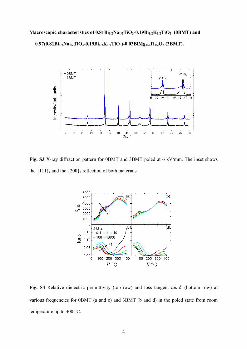
Macroscopic characteristics of 0.81Bi1/2Na1/2TiO3-0.19Bi1/2K1/2TiO3 (0BMT) and
0.97(0.81Bi1/2Na1/2TiO3-0.19Bi1/2K1/2TiO3)-0.03BiMg1/2Ti1/2O3 (3BMT).
Fig. S3 X-ray diffraction pattern for 0BMT and 3BMT poled at 6 kV/mm. The inset shows
the {111}c and the {200}c reflection of both materials.
Fig. S4 Relative dielectric permittivity (top row) and loss tangent tanδ (bottom row) at
various frequencies for 0BMT (a and c) and 3BMT (b and d) in the poled state from room
temperature up to 400 °C.

5
Increased reliability of the image and reduced topographical crosstalk of dual AC
resonance tracking in the cantilever's torsional vibration mode.
The Fig. S5 shows the phase response of the same area measured by SF- (a) and TDART-(b)
PFM, as well as the respective cross-sectional profiles (c). Both images feature two dominant
phase values that can be attributed to the two possible domain orientations in the particular
direction of the observation. A bright dot (encircled by the blue circle) directly below the
central domain is visible in the SF-PFM image. Highlighted by the blue ellipse and the arrows
in the cross-section, the phase profile measured by SF-PFM clearly deviates from the profile
obtained by TDART with a bump/hollow combination rather than a flat area at the same
position. The associated topography image (see inset of Fig. S5(c)) exhibits a hole
approximately 500 pm in depth at this exact position. For clarity, we added the topographical
profile into the cross-section, which indicates the correlation between the height and phase. In
the case of the SF-PFM technique, this artifact was caused by topographical crosstalk induced
by the feedback loop keeping the mean deflection signal constant during scanning. At the
falling edge, the deflection of the cantilever changes to lower values, forcing the z-piezo to
move the tip towards the sample surface to trace the topography. A sloped topography,
however, can only be tracked with residual error. As a consequence, the contact resonance
shifts to lower frequencies and hence the phase shifts to larger values compared to the contact
resonance corresponding to the given deflection set point (note that the phase data shown in
Fig S5 corresponds to the retrace curve, i.e., the scan direction was from right to left). At the
rising edge, the topography error has the opposite sign; thus, the contact resonant frequency
shifts to higher values and smaller phase shifts. These variations lead to a wave-like shape of
the phase shift profile in SF-PFM as shown in Fig. S5(a). In TDART mode, however, this
artifact is corrected by the additional feedback loop tracking the instantaneous contact
resonance. In addition, the slope derived from the phase profile obtained by TDART (red) is
higher than that measured by the SF technique at the right domain wall between the central
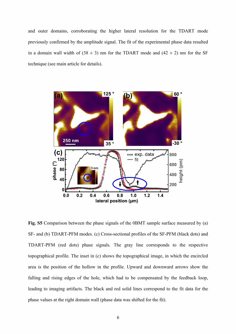
6
and outer domains, corroborating the higher lateral resolution for the TDART mode
previously confirmed by the amplitude signal. The fit of the experimental phase data resulted
in a domain wall width of (38 ± 3) nm for the TDART mode and (42 ± 2) nm for the SF
technique (see main article for details).
Fig. S5 Comparison between the phase signals of the 0BMT sample surface measured by (a)
SF- and (b) TDART-PFM modes. (c) Cross-sectional profiles of the SF-PFM (black dots) and
TDART-PFM (red dots) phase signals. The gray line corresponds to the respective
topographical profile. The inset in (c) shows the topographical image, in which the encircled
area is the position of the hollow in the profile. Upward and downward arrows show the
falling and rising edges of the hole, which had to be compensated by the feedback loop,
leading to imaging artifacts. The black and red solid lines correspond to the fit data for the
phase values at the right domain wall (phase data was shifted for the fit).
7
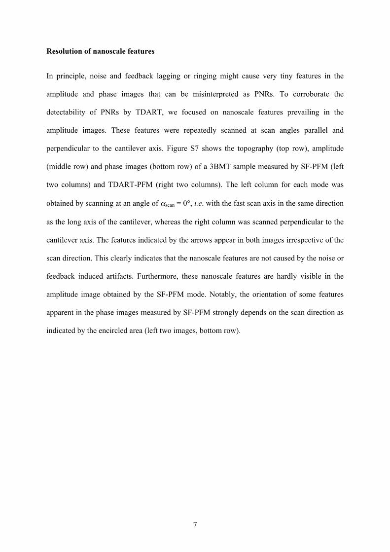
Resolution of nanoscale features
In principle, noise and feedback lagging or ringing might cause very tiny features in the
amplitude and phase images that can be misinterpreted as PNRs. To corroborate the
detectability of PNRs by TDART, we focused on nanoscale features prevailing in the
amplitude images. These features were repeatedly scanned at scan angles parallel and
perpendicular to the cantilever axis. Figure S7 shows the topography (top row), amplitude
(middle row) and phase images (bottom row) of a 3BMT sample measured by SF-PFM (left
two columns) and TDART-PFM (right two columns). The left column for each mode was
obtained by scanning at an angle of αscan = 0°, i.e. with the fast scan axis in the same direction
as the long axis of the cantilever, whereas the right column was scanned perpendicular to the
cantilever axis. The features indicated by the arrows appear in both images irrespective of the
scan direction. This clearly indicates that the nanoscale features are not caused by the noise or
feedback induced artifacts. Furthermore, these nanoscale features are hardly visible in the
amplitude image obtained by the SF-PFM mode. Notably, the orientation of some features
apparent in the phase images measured by SF-PFM strongly depends on the scan direction as
indicated by the encircled area (left two images, bottom row).

8
Fig. S6. Comparison between the SF-PFM (left column) and the TDART techniques (right
column). Shown are the topography (top row), amplitude (middle row) and phase (bottom
row) images obtained on piezoelectric standard material PIC 151 (lead-zirconate-titanate,
PZT). The TDART amplitude image clearly reveals a riffled structure that could not be
resolved by SF-PFM (see locations indicated by the arrows). The corresponding phase images
exhibit the same lateral distribution of ferroelectric in-plane domains.

9
Fig. S7 Comparison between the SF-PFM mode (left two columns) and the TDART
technique (right two colums). Topography (top row), amplitude (middle) and phase (bottom)
images of a 3BMT sample. The images were measured in different scan directions as noted at
the bottom. Arrows indicate similar features that are independent of the scan direction with
respect to the sample, whereas the encircled areas highlight a region showing a domain
orientation that indeed depends on the scan direction. Color bars: topography 0–8 nm,
amplitude arbitrary, phase -19–58 °, -16–54 °, 53–233 °, 48–228 ° (from left to right).