supplementary materials for - mit.edumingdao/papers/2018_science_diamond_ultralarge... · sequences...
TRANSCRIPT
www.sciencemag.org/content/360/6386/300/suppl/DC1
Supplementary Materials for
Ultralarge elastic deformation of nanoscale diamond
Amit Banerjee,* Daniel Bernoulli,* Hongti Zhang,* Muk-Fung Yuen, Jiabin Liu, Jichen Dong, Feng Ding, Jian Lu, Ming Dao,† Wenjun Zhang,† Yang Lu,† Subra Suresh†
*These authors contributed equally to this work.
†Corresponding author. Email: [email protected] (M.D.); [email protected] (W.Z.); [email protected] (Y.L.); [email protected] (S.S.)
Published 20 April 2018, Science 360, 300 (2018)
DOI: 10.1126/science.aar4165
This PDF file includes:
Materials and Methods Supplementary Text Figs. S1 to S10 Table S1 Captions for Movies S1 to S6 References
Other Supplementary Material for this manuscript includes the following: (available at www.sciencemag.org/content/360/6386/300/suppl/DC1)
Movies S1 to S6

Materials and Methods
Sample Fabrication and Materials Characterization Nanoscale diamond needles used in the present study were fabricated by bias-assisted
reactive ion etching (RIE) of diamond thin films deposited on Si substrates through plasma-enhanced chemical vapor deposition (CVD) (5). A gas mixture of CH4 (0.5-10%)/H2 was used for generating microwave plasma at a pressure of 30 Torr (or ~ 4 kPa). The Si substrates were pre-scratched with diamond powder (~250 nm) paste to enhance nucleation. The growth rate and quality of the film, e.g., grain-size and crystallinity, are highly sensitive to growth parameters adopted during the deposition process. For example, high CH4 concentration led to the deposition of nanodiamond films, whereas low CH4 concentration generated polycrystalline films with micrometer size grains. Following the CVD process, a bias-assisted RIE was carried out by subjecting the diamond thin films in microwave plasma (2 × 10⁻³ Torr or ~ 0.27 Pa) formed with gas mixture of Ar, He, and N2 under a negative substrate bias, in which both ion-induced sputtering and reactive etching led to the formation of diamond surface nanostructures, e.g., nanoneedles. The shape and density of diamond nanoneedles could be controlled by appropriately modulating the RIE parameters, e.g., gas composition, pressure, and bias voltage. Further details of the deposition and RIE processes can be found elsewhere (5, 26). Lastly, the samples were further treated in hydrogen plasma for 1 h at a pressure of 30 Torr and substrate temperature of 800 oC to remove the amorphous carbon formed during RIE process.
The shape, size, crystallinity, and density of the nanoneedles were controlled by appropriate choice of growth and etching parameters. The single-crystalline diamond nanoneedles (Fig. S1) were etched from a polycrystalline diamond film with enriched <111> planes exposed. We ascertained the crystallinity (Fig. S1A) of the nanoneedles by recourse to electron diffraction experiments, and verified their sp3 hybridized C-C bond structure (Fig. S1B) by using micro-Raman spectroscopy. We also performed additional HRTEM characterization for another typical <111>-oriented diamond nanoneedle (see Fig. S2), and verified that the amorphous/graphitic layer over the diamond nanoneedle surface was indeed very thin (averaging ~2 nm thick or less, versus the 160-230 nm diameter of diamond nanoneedles at the maximum strain location), while the crystalline structure was rather clean with very few defects. Negligible impact (within 0.2% strain difference) towards the maximum tensile strain estimation due to the very thin and elastically softer amorphous layer is estimated from FEM simulations. Together with the SAED pattern, the above mutually consistent results verify that our nanoneedles are indeed single crystalline diamond.
The polycrystalline nanoneedles were constructed from nanodiamond films using the same bias-assisted RIE method, and they comprised randomly oriented crystallites with an average grain size of approximately 10 nm.
Experimental Method
The diamond nanoneedles on the Si substrate were mounted inside a SEM nanoindenter system (Fig. 1A) for quantitative in-situ nanomechanical characterization. Fig. 1B shows a close up view of the alignment of the ‘cube-corner’ diamond tip of the nanoindenter and a free-standing diamond nanoneedle, which was achieved to a precision of about 7 nm through in- and out-of-plane translation of the nanoneedles by controlling the piezoelectric sample stage. When one side of the indenter tip, i.e., the cube-corner with an included angle of 90 deg, establishes contact with the diamond nanoneedle, the downward motion of the tip generates a sideward displacement from the inclined indenter tip surface, thereby bending the nanoneedle (a schematic

representation of the process is presented in Fig. 1C). Fig. 1D shows an image obtained in a high-resolution transmission electron microscope (HRTEM) showing its smooth surface and the pristine single-crystalline diamond structure along the <111> growth orientation aligned with the nanoneedle axis. When the bending of the nanoneedle by the indenter tip was carried all the way to final failure, the ensuing fracture mode was brittle, as anticipated for diamond (Fig. 1E).
A quantitative picoindentor Hysitron PI85 nanoindenter system (Hysitron, Eden Prairie, MN, U.S.A.) was mounted inside a scanning electron microscope (SEM, FEITM Quanta FEG 450, Hillsboro, OR, U.S.A.). The indenter system was attached to the SEM stage so that its position could be controlled by moving the SEM stage through 3-axis translation, rotation, and tilt. The operations with the PI85 system, such as the movement of the sample stage or the cube-corner indentation tip was controlled externally through electrical communication via feed-through channels going into the SEM chamber without affecting the vacuum condition. The Si substrate containing the diamond nanoneedles was mounted onto the PI85 stage and brought into the field of view by precisely controlling the position of the stage. The piezoelectric stage of the PI85 system can be moved in x, y, and z directions (within a spatial precision of ~ 7 nm) until a diamond nanoneedle chosen for mechanical experiment is brought underneath the cube-corner tip of the indenter. The bending experiments were subsequently carried out under the control of the TriboScanTM software incorporated into the PI85 system.
FEM computation, which simulated elastic deformation for the actual indenter tip and nanoneedle geometries used in our experiment, invoked analyses of nonlinear elasticity, elastic anisotropy (Fig. S3), as well as frictional contact conditions between the indenter tip and nanoneedle. Here, geometric nonlinearity induced by large bending deformation and rotation was fully accounted for. From these simulations, we extracted the strain distribution and the maximum strain achievable in the diamond nanoneedles prior to final fracture from bending. The exact geometry of each individual diamond needle, determined from our experimental observations, was modeled in the numerical simulations. Given the axisymmetric shape of the diamond needle, the indentation displacement after the initial contact between the indenter tip and the nanoneedle correlates with the extent of sideward bending of the needle. The mechanics of such deformation is analyzed and quantified here from the data on indentation force as a function of the vertical indenter tip displacement from the experiments and the FEM simulation. In order to account for the effect of friction between the indenter tip and the diamond nanoneedle on the maximum tensile or compressive strain of the latter during bending, the simulations were carried out using friction coefficients, f, between 0.1 and 1.0 (Fig. S4). These values were chosen based on observation (19) that the friction coefficient for diamond on diamond in low-pressure environments, such as the one existing inside the electron microscope, can be significantly larger than that measured in ambient air (21). Further details of the FEM simulation can be found below. Finite element method (FEM) simulations for evaluating the experimental elastic strains
FEM was used to simulate flexural deformation and to determine the strain and stress distribution of the nanoneedles during bending, based on the nanoneedle bending experiments data. The simulations were carried out using the commercially available AutoCAD (Autodesk, Inc., San Rafael, CA, U.S.A.) and ABAQUS (Dassault Systèmes Simulia Corp., Providence, RI, U.S.A.) software packages. The analyses invoked displacement-control conditions for each individual nanoneedle shape and geometry characterized experimentally. Both the diamond indenter tip and the diamond nanoneedles were treated as elastically deformable, with frictional

contact between them incorporated in the analyses. Since cubic elasticity anisotropy does not influence the elastic deformation of <111>-oriented nanoneedles (see results in Fig. S3 using anisotropic elasticity data taken from (27)), isotropic elasticity parameters were taken for the diamond nanoneedles. To take into account the nonlinear elastic deformation beyond about 2%, the Neo-Hookean nonlinear elasticity model, instead of linear elasticity model, was used in the simulations, with the Neo-Hookean material parameters C10=257 GPa and D1=5.45x10⁻³ GPa-1 (28). The equivalent small strain linear elasticity parameters are: Young’s modulus E = 1100 GPa and Poisson’s ratio ν = 0.07 (10). The strain distribution, as well as the extracted maximum elastic strain, of a deformed diamond nanoneedle is primarily determined by the indentation displacement (and the corresponding flexural deformation); our results show that they are not sensitive to variations in elastic modulus (Table S1) and friction coefficient (Fig. S4).
We had managed to conduct a few measurements by direct compression using a flat-punch indenter tip on top-flatted nanoneedles, and extracted Young’s modulus value upon unloading to be 1010 ± 55 GPa, quite close to the commonly reported values between 1000-1100GPa (10).
In addition, we also evaluated the stress state at and near the maximum principal strain sites (on the surface and within 10% diameter below surface) for each single-crystalline nanoneedle case we presented in Fig. 4 – they are all practically purely tensile (i.e. the magnitudes of the medium and minimum principal stresses are all less than 0.2% of the maximum principal stress). Therefore the extracted maximum principal (tensile) elastic strain from FEM simulations is equivalent to maximum elastic tensile strain within the nanoneedles.
Additional Experiments on Single Crystalline Diamond Nanoneedles (lateral pushing and buckling cases)
We have performed five additional experiments pushing nanoneedles purely sideward where a cube-corner diamond tip in a pure lateral motion pushes the vertical needles, and still produced the comparable amount of bending as that produced by the downward pushing using indenter side surface. The results are summarized in Fig. S6, again showing very large maximum elastic tensile strains. With f = 0.1, the extracted maximum tensile strains from FEM simulations are evaluated to be 4.73%, 4.48% and 3.76% for three reversible runs, and 4.63% and 4.69% for the fracture runs, respectively.
We also performed additional experiments trying to push the indenter tip directly “punching a nanoneedle”. However, when we did that, the nanoneedle would experience the buckling behavior due to the long aspect-ratio. The unpredictable buckling bulging direction makes it very difficult to evaluate precisely the exact geometrical changes, and consequently the exact maximum strain of the nanoneedle. Therefore this loading mode was deemed not worth further pursuing for the purpose of this study. Experiments on Polycrystalline Diamond Nanoneedle Specimens
We also performed in-situ bending experiments on polycrystalline diamond nanoneedle specimens similar to those on single-crystalline specimens. An electron diffraction pattern showing the polycrystalline structure of the nanoneedle is shown in Fig. S7A. Fig. 3A-C show sequences of images of a typical polycrystalline nanoneedle undergoing flexural deformation. Unlike the single-crystalline nanoneedles, fracture surfaces in polycrystalline nanoneedles were observed to be nearly parallel to the substrate (Fig. 3C). The maximum deflection of the polycrystalline diamond nanoneedle just prior to fracture is seen to be about 267 nm (~ 21% of the needle’s length) in Fig. 3B, and the fractured nanoneedle is shown in Fig. 3C. Fig. S7B

shows the corresponding variation of imposed load versus displacement for the polycrystalline nanoneedle. The local (tensile) maximum principal strain estimated from FEM simulation is between 3.51% (with f = 1.0) and 3.54% (with f = 0.1, see also Fig. S7C) for the polycrystalline needle, which is approximately one half that for the single-crystalline nanoneedle. The predicted maximum horizontal deflection before fracture from FEM simulation is 272 nm (with f = 1.0) and 275 nm (with f = 0.1), as compared to 267 nm measured experimentally. Fig. S8 reveals a sequence of images from initial loading to final fracture of another typical polycrystalline diamond nanoneedle, with deformation characteristics similar to those observed in Fig. 3 and Fig. S7. Four fracture experiments were successfully carried out on four different polycrystalline diamond nanoneedles, with appreciable maximum tensile elastic strains achieved in each case. Density Functional Theory - Molecular Dynamics (DFT-MD) simulations for evaluating the theoretical tensile strain of diamond
The DFT–MD simulations, implemented using the Vienna ab initio simulation Package (VASP) (29, 30), were carried out to investigate the theoretical tensile properties of single crystalline diamond. The local density approximation (LDA) was adopted for the exchange–correlation functional (31). The K-point mesh was sampled by 1×1×1. During the simulations, the temperature was fixed at 300 K and the time step was 0.5 fs. The diamond nanowire was stretched along its axial direction (along a <111>-orientation) by 1% for every 500 MD steps. During each relaxation stage, the canonical ensemble (also called the NVT ensemble, which is a statistical ensemble wherein the number of atoms, N, the volume, V, and the temperature, T, are kept constant during the simulation) was used.
Density functional theory (DFT) calculations (32) have suggested an ideal strength of ~ 100 GPa for diamond, which corresponds to an elastic strain of about 10% at the elastic limit. These calculations were performed by recourse to static structural relaxation, and neglected the thermal fluctuation effect at finite temperature and the resultant defect activation processes (33). Furthermore, owing to the limited accuracy of the force field models, classical molecular dynamics (MD) simulations of the fracture of diamond nanowires that involves the breaking of C–C covalent bonds do not adequately capture experimental trends of mechanical deformation (34). In order to overcome these limitations of classical approaches, we conducted DFT–MD simulations (Fig. S9A-B) which allowed us to include the temperature effect to explore the critical strain of diamond nanowire along the <111> direction more precisely. The simulation results showed that the tensile stress reached its maximum at the critical strain of ~ 13% and C–C bond fracture occurred beyond this critical strain (Fig. S9B). The DFT–MD model predicted that the true stress versus true strain curve is roughly linear with a small reduction in slope beyond ~ 7% strain before the maximum stress reached ~ 13%. Note that in the FEM simulation, nonlinear Neo-Hookean elasticity was used, which matches reasonably well with (while slightly stiffer than) the response predicted by DFT–MD.
Maximum Compressive Elastic Strains Extracted The same procedure was used to extract the maximum elastic compressive strains (Fig. S10) from each experiment as for the maximum elastic tensile strains, except that the local maximum elastic compressive strain values were extracted from the minimum principal strain ( ) distribution plots obtained from the corresponding FEM simulations.

Supplementary Text Discussion on the Bending, Tension and Compression Experiments
For bulk brittle materials, the flexural strength of a brittle material is on the same order of magnitude as the tensile strength, while the tensile strength is generally one order of magnitude lower than the compressive strength (see Table 8.2 in (35)). A bending experiment involves both tensile and compressive stresses. For a brittle nano-sized material, we still expect to see significantly lower tensile strength than compressive strength, and consequently failure in a bending test initiates at the tensile side of the deflected sample. Thus for a brittle material the bending experiment is considered to be a good alternative test for a tensile experiment, especially given the complexity of performing such experiments for nano-scale specimens inside a microscope.
An earlier study in the literature (22) reported high compressive engineering strength of nano-sized diamond to be up to 250 GPa for <111> oriented samples, and the corresponding maximum engineering strain is ~17%. The authors gave caution to their strain data, since “true strain could not be determined with perfect accuracy” (22). These compressive stress and strain values are on the same order of magnitude as we observed on the compression side (Fig. S10). Since the failure initiates on the tensile side for the nanoneedles, what we observed in Fig. S10 are conservative estimates of the achievable compressive strains. Our bending experiments, however, provide more precise estimates of both the maximum tensile and compressive strains achieved in the sample, since these strains can be quite accurately extracted from the in-situ observations of the flexural deformation.
The bending tests do reveal that ultra-large elastic tensile strains (up to 9%) can be actually achieved in diamond. Possible Origins of Ultrahigh Elasticity: Paucity of Internal Defects and Smooth Surfaces
The experimentally observed ultrahigh elasticity of the diamond nanoneedles can be ascribed to two factors. The first is the nanoscale size of the diamond needles. The concept of “ultra-strength” materials (13, 36, 37), defined as materials that can be engineered to sustain one-tenth or a greater proportion of the theoretical strength (obtained at 0 K for a 100% perfect crystal) for an extended period of time (13, 36, 37), has been realized in a number of crystalline materials at the nanoscale (38-42). In nanometer sized samples, owing to their small dimensions, the concentration of defects and pre-existing faults (e.g. cracks) is far less than in micro-scale specimens and dislocation nucleation is far more restricted (43), making them “ultra-strong”. Due to their extremely small volumes, the number of potential dislocation sources in the pristine single-crystalline diamond nanoneedles is also severely limited. Even with a few initial dislocations present, dislocations in diamond nanoneedles can only travel very short distances, because of very small specimen dimensions, before being eliminated at the free surfaces, thereby further reducing the overall dislocation multiplication rate and dislocation density. These effects significantly increase the elastic limit, and delay the onset of plasticity and fracture. Such processes can lead to a dislocation-starved state, thereby requiring very high stresses to nucleate new mobile dislocations, leading to “ultra-strength” (13). In our experiments, the high quality CVD fabrication method provides the single-crystalline nanoneedles with a pristine, defect-scarce state (Fig. 1D).
Secondly, brittle fracture, typically seen in diamond, inevitably requires crack initiation at some local weak point or a heterogeneous surface imperfection, without any contribution from

dislocations (44), as the precursor to catastrophic failure. However, the nanoscale smooth surface (see Fig. 1D and Figs. S1-S2) of the diamond nanoneedle makes it harder to initiate such a crack by homogeneous nucleation through the breaking of atomic bonds. Possible factors of the observed scatter in maximum tensile strains of diamond nanoneedles Brittle materials usually are associated with a scatter in their failure stress / strain, and it is normally originated in a manner that is strongly dependent on statistics of the internal or surface defect distribution. In our case, inherent variations in sample microstructure, surface roughness, shapes and needle dimensions could give rise to the observed scatter in the data. In addition, it may also relate to the particular distribution of the thin amorphous layer in each nanoneedle (Fig. S2). We note that Weibull scatter for an average failure strain of 0.2-0.36% observed in bulk diamond in the literature (10-12, 21) simply cannot explain the observed 4-9% maximum elastic tensile strains observed in single crystalline diamond nanoneedles. Even the lower values of elastic tensile strains of about 4% obtained in this study are still one order of magnitude higher than the commonly observed bulk diamond elastic limit, estimated to be ~ 0.36% (21).

Fig. S1. Selected Area Electron Diffraction (SAED) and Raman spectroscopy characterization of single-crystalline diamond nanoneedles. (A) Bright field TEM showing the conical shape of a diamond nanoneedle sample. Inserted electron diffraction pattern shows the <111>-oriented diamond crystal structure for the corresponding nanoneedle in the main image. (B) micro-Raman spectra of the diamond film and the diamond nanoneedles. The overlap of the characteristic peak at 1332 cm-1 confirms the sp3 diamond phase of the samples (45)
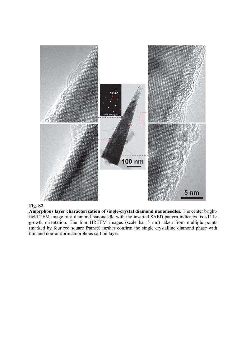
Fig. S2 Amorphous layer characterization of single-crystal diamond nanoneedles. The center bright-field TEM image of a diamond nanoneedle with the inserted SAED pattern indicates its <111> growth orientation. The four HRTEM images (scale bar 5 nm) taken from multiple points (marked by four red square frames) further confirm the single crystalline diamond phase with thin and non-uniform amorphous carbon layer.

Fig. S3 Effect of elasticity anisotropy toward estimated local maximum elastic tensile strain achieved within a single-crystalline sample (the nanoneedle shown in Fig. 2). The isotropic FEM simulations were carried out assuming Young’s modulus E = 1100 GPa and Poisson’s ratio ν = 0.07, with diamond-diamond friction coefficient f = 0.1. For the anisotropic FEM simulations, the exact cubic elasticity anisotropy was used with the [111]-orientation as the nanoneedle axis and 5 different rotational positions (0, 22.5. 45, 67.5, 90 degrees) with respect to the [111] axis. It was observed that the extracted maximum elastic strains are virtually identical (within ± 0.1%). Note that these results are expected, since for transversely isotropic elastic materials, there should be no orientation dependence of the elastic deformation when the sample is rotated with respect to the [111] axis.

Fig. S4 Effect of friction coefficient toward estimated maximum local elastic tensile strain achieved within a single crystalline diamond nanoneedle. FEM simulations were performed to simulate the bending deformation in a diamond nanoneedle and extract the local maximum elastic tensile strain, assuming different friction coefficient values between 0.1 and 1.0. Only small differences (less than 1%) were found.

Fig. S5 Bending of a single crystalline diamond nanoneedle with the lowest maximum local elastic tensile strain among single crystal samples loaded to fracture. (A) Initial contact of the diamond indenter tip and the nanoneedle. (B-D) Sequential SEM images showing the maximum bending state before the fracture, the initiation of the fracture of the diamond nanoneedle, and the video frame immediately after the fracture, respectively. (E) The corresponding indenter tip load versus vertical displacement curve. (F) FEM simulation showing the nanoneedle at the maximum bending deformation right before fracture, with the highest maximum local elastic tensile strain estimated to be 3.87%. Friction coefficient was taken as f = 0.1.

Fig. S6 Summary of the results extracted from pure lateral pushing experiments, where the bending of nanoneedles were produced by a horizontal movement of the indenter tip. (A) Schematic drawing of the experimental configuration. (B) SEM images from a reversible run by lateral pushing of the nanoneedle. (C) FEM simulation showing the nanoneedle at the maximum bending deformation, corresponding the middle image shown in (B), with the maximum local elastic tensile strain shown to be 4.73%. (D) Summary of extracted maximum elastic tensile strain values from the five lateral pushing experiments, using FEM simulations assuming friction coefficient as f = 0.1 or 1.0.
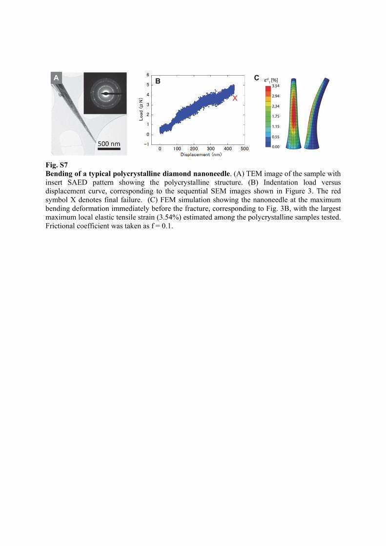
Fig. S7 Bending of a typical polycrystalline diamond nanoneedle. (A) TEM image of the sample with insert SAED pattern showing the polycrystalline structure. (B) Indentation load versus displacement curve, corresponding to the sequential SEM images shown in Figure 3. The red symbol X denotes final failure. (C) FEM simulation showing the nanoneedle at the maximum bending deformation immediately before the fracture, corresponding to Fig. 3B, with the largest maximum local elastic tensile strain (3.54%) estimated among the polycrystalline samples tested. Frictional coefficient was taken as f = 0.1.
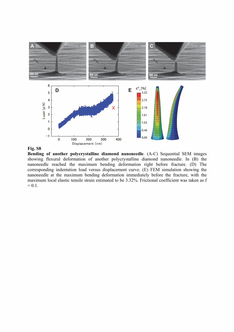
Fig. S8 Bending of another polycrystalline diamond nanoneedle. (A-C) Sequential SEM images showing flexural deformation of another polycrystalline diamond nanoneedle. In (B) the nanoneedle reached the maximum bending deformation right before fracture. (D) The corresponding indentation load versus displacement curve. (E) FEM simulation showing the nanoneedle at the maximum bending deformation immediately before the fracture, with the maximum local elastic tensile strain estimated to be 3.32%. Frictional coefficient was taken as f = 0.1.
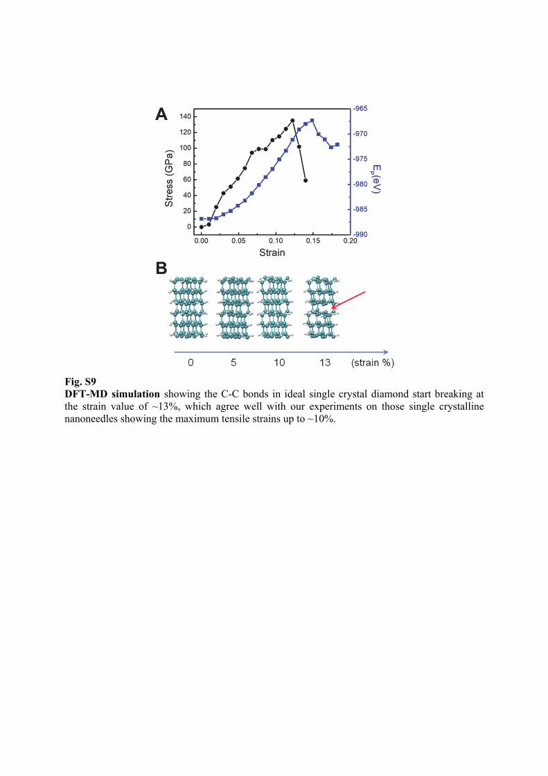
Fig. S9 DFT-MD simulation showing the C-C bonds in ideal single crystal diamond start breaking at the strain value of ~13%, which agree well with our experiments on those single crystalline nanoneedles showing the maximum tensile strains up to ~10%.

Fig. S10 Summary of the maximum elastic compressive strains. The results were extracted by FEM analysis on the basis of nanoneedle bending experiments, assuming friction coefficient f = 1.0 or 0.1. The data from eight experiments with five different single-crystalline samples (final fracture and fully reversible runs shown by red and brown data points, respectively) and four experiments with four different polycrystalline samples (shown by green circles) are presented.

E<111> (GPa) εmax (%) Δεmax vs 8.88% σmax (GPa)
900 8.918 0.038% 80 1000 8.903 0.023% 89 1100 8.880 0.000% 98 1200 8.877 ‐0.003% 107
Table S1 Dependence on the nanoneedle’s Young’s modlus taken in FEM simulations, for the extracted maxmum tensile strain and maximum stress values. The parametric FEM simulations were done using different values of elastic modulus along <111> (E<111>) for the diamond nanoneedle final fracture run shown in Fig. 2B, and the corresponding maximum elastic tensile strains (εmax) and maximum tensile (σmax) are shown. The difference in εmax versus the value extracted assuming E<111> = 1100 GPa was also listed, showing virtually no changes in maximum strains obtained when assuming different modulus values. The maximum stresses, however, do vary proportionally with the modulus values. By default, E<111> = 1100 GPa was assumed for all FEM simulations in the present study, unless specified otherwise.
Supplementary Movie Captions: Movie S1 Bending of a single crystalline diamond nanoneedle inside SEM, with fully recoverable flexural deformation (shown in Fig. 2A (A1 – A4)); video speed at 10 times the speed of experiment. Movie S2 Bending of a single crystalline diamond nanoneedle inside SEM, with final fracture (shown in Fig. 2B (B1 – B4)); video speed at 15 times the speed of experiment. The extracted maximum local (tensile) elastic strain is the highest (~9%) among all tested samples. Movie S3 Bending of another single crystalline diamond nanoneedle inside SEM, with final fracture (shown in Fig. S5A–D); video speed at 16 times the speed of experiment. Movie S4 Bending of a single crystalline diamond nanoneedle inside SEM pushed by a lateral sideward movement of the indenter tip, with fully recoverable flexural deformation (shown in Fig. S6); video speed at 8 times the speed of experiment. Movie S5 Bending of a polycrystalline diamond nanoneedle inside SEM, with final fracture (shown in Fig. 3A–C) and S7); video speed at 11 times the speed of experiment. Movie S6 Bending of another polycrystalline diamond nanoneedle inside SEM, with final fracture (shown in Fig. S8A–C); video speed at 11 times the speed of experiment.

References and Notes 1. A. L. Robinson, Is diamond the new wonder material? Science 234, 1074–1076 (1986).
doi:10.1126/science.234.4780.1074 Medline
2. W. Zhu, G. P. Kochanski, S. Jin, Low-field electron emission from undoped nanostructured diamond. Science 282, 1471–1473 (1998). doi:10.1126/science.282.5393.1471 Medline
3. I. Aharonovich, A. D. Greentree, S. Prawer, Diamond photonics. Nat. Photonics 5, 397–405 (2011). doi:10.1038/nphoton.2011.54
4. V. N. Mochalin, O. Shenderova, D. Ho, Y. Gogotsi, The properties and applications of nanodiamonds. Nat. Nanotechnol. 7, 11–23 (2011). doi:10.1038/nnano.2011.209 Medline
5. X. Zhu, M. F. Yuen, L. Yan, Z. Zhang, F. Ai, Y. Yang, P. K. N. Yu, G. Zhu, W. Zhang, X. Chen, Diamond-nanoneedle-array-facilitated intracellular delivery and the potential influence on cell physiology. Adv. Healthc. Mater. 5, 1157–1168 (2016). doi:10.1002/adhm.201500990 Medline
6. Y. Wang, Y. Yang, L. Yan, S. Y. Kwok, W. Li, Z. Wang, X. Zhu, G. Zhu, W. Zhang, X. Chen, P. Shi, Poking cells for efficient vector-free intracellular delivery. Nat. Commun. 5, 4466 (2014). Medline
7. X. Chen, W. Zhang, Diamond nanostructures for drug delivery, bioimaging, and biosensing. Chem. Soc. Rev. 46, 734–760 (2017). doi:10.1039/C6CS00109B Medline
8. K. Tanigaki, H. Ogi, H. Sumiya, K. Kusakabe, N. Nakamura, M. Hirao, H. Ledbetter, Observation of higher stiffness in nanopolycrystal diamond than monocrystal diamond. Nat. Commun. 4, 2343 (2013). doi:10.1038/ncomms3343 Medline
9. Q. Huang, D. Yu, B. Xu, W. Hu, Y. Ma, Y. Wang, Z. Zhao, B. Wen, J. He, Z. Liu, Y. Tian, Nanotwinned diamond with unprecedented hardness and stability. Nature 510, 250–253 (2014). doi:10.1038/nature13381 Medline
10. J. E. Field, The Properties of Natural and Synthetic Diamond (Academic Press, 1992).
11. M. Seal, Graphitization and plastic deformation of diamond. Nature 182, 1264–1267 (1958). doi:10.1038/1821264a0
12. R. J. Hemley, H. Mao, G. Shen, J. Badro, P. Gillet, M. Hanfland, D. Häusermann, X-ray imaging of stress and strain of diamond, iron, and tungsten at megabar pressures. Science 276, 1242–1245 (1997). doi:10.1126/science.276.5316.1242
13. T. Zhu, J. Li, Ultra-strength materials. Prog. Mater. Sci. 55, 710–757 (2010). doi:10.1016/j.pmatsci.2010.04.001
14. J. Li, Z. Shan, E. Ma, Elastic strain engineering for unprecedented materials properties. MRS Bull. 39, 108–114 (2014). doi:10.1557/mrs.2014.3
15. D. Yu, J. Feng, J. Hone, Elastically strained nanowires and atomic sheets. MRS Bull. 39, 157–162 (2014). doi:10.1557/mrs.2014.6
16. V. M. Pereira, A. H. Castro Neto, Strain engineering of graphene’s electronic structure. Phys. Rev. Lett. 103, 046801 (2009). doi:10.1103/PhysRevLett.103.046801 Medline

17. H. Watanabe, C. E. Nebel, S. Shikata, Isotopic homojunction band engineering from diamond. Science 324, 1425–1428 (2009). doi:10.1126/science.1172419 Medline
18. Materials and methods are available as supplementary materials.
19. Z. Feng, Y. Tzeng, J. E. Field, Friction of diamond on diamond in ultra-high vacuum and low-pressure environments. J. Phys. D Appl. Phys. 25, 1418–1424 (1992). doi:10.1088/0022-3727/25/10/006
20. R. H. Telling, C. J. Pickard, M. C. Payne, J. E. Field, Theoretical strength and cleavage of diamond. Phys. Rev. Lett. 84, 5160–5163 (2000). doi:10.1103/PhysRevLett.84.5160 Medline
21. J. E. Field, The mechanical and strength properties of diamond. Rep. Prog. Phys. 75, 126505 (2012). doi:10.1088/0034-4885/75/12/126505 Medline
22. J. M. Wheeler, R. Raghavan, J. Wehrs, Y. Zhang, R. Erni, J. Michler, Approaching the limits of strength: measuring the uniaxial compressive strength of diamond at small scales. Nano Lett. 16, 812–816 (2016). doi:10.1021/acs.nanolett.5b04989 Medline
23. P. Ovartchaiyapong, K. W. Lee, B. A. Myers, A. C. B. Jayich, Dynamic strain-mediated coupling of a single diamond spin to a mechanical resonator. Nat. Commun. 5, 4429 (2014). doi:10.1038/ncomms5429 Medline
24. S. Dhomkar, J. Henshaw, H. Jayakumar, C. A. Meriles, Long-term data storage in diamond. Sci. Adv. 2, e1600911 (2016). doi:10.1126/sciadv.1600911 Medline
25. B. Khanaliloo, H. Jayakumar, A. C. Hryciw, D. P. Lake, H. Kaviani, P. E. Barclay, Single-crystal diamond nanobeam waveguide optomechanics. Phys. Rev. X 5, 041051 (2015). doi:10.1103/PhysRevX.5.041051
26. B. He, Y. Yang, M. F. Yuen, X. F. Chen, C. S. Lee, W. J. Zhang, Vertical nanostructure arrays by plasma etching for applications in biology, energy, and electronics. Nano Today 8, 265–289 (2013). doi:10.1016/j.nantod.2013.04.008
27. G. Simmons, H. Wang, Single Crystal Elastic Constants and Calculated Aggregate Properties: A Handbook (The MIT Press, 1971).
28. Dassault Systèmes Simulia, ABAQUS 6.14 Theory Guide, Section 4.6.1, Hyperelastic Material Behavior (Dassault Systèmes, 2014); http://abaqus.software.polimi.it/v6.14/books/stm/ch04s06ath123.html.
29. G. Kresse, J. Hafner, Ab initio molecular dynamics for open-shell transition metals. Phys. Rev. B 48, 13115–13118 (1993). doi:10.1103/PhysRevB.48.13115 Medline
30. G. Kresse, J. Furthmüller, Efficiency of ab-initio total energy calculations for metals and semiconductors using a plane-wave basis set. Comput. Mater. Sci. 6, 15–50 (1996). doi:10.1016/0927-0256(96)00008-0
31. J. P. Perdew, A. Zunger, Self-interaction correction to density-functional approximations for many-electron systems. Phys. Rev. B 23, 5048–5079 (1981). doi:10.1103/PhysRevB.23.5048
32. D. Roundy, M. L. Cohen, Ideal strength of diamond, Si, and Ge. Phys. Rev. B 64, 212103 (2001). doi:10.1103/PhysRevB.64.212103

33. J. Li, The mechanics and physics of defect nucleation. MRS Bull. 32, 151–159 (2007). doi:10.1557/mrs2007.48
34. L. Pastewka, S. Moser, M. Moseler, Atomistic insights into the running-in, lubrication, and failure of hydrogenated diamond-like carbon coatings. Tribol. Lett. 39, 49–61 (2010). doi:10.1007/s11249-009-9566-8
35. M. A. Meyers, K. K. Chawla, Mechanical Behavior of Materials (Cambridge Univ. Press, ed. 2, 2009).
36. S. Suresh, J. Li, Materials science: Deformation of the ultra-strong. Nature 456, 716–717 (2008). doi:10.1038/456716a Medline
37. T. Zhu, J. Li, S. Ogata, S. Yip, Mechanics of ultra-strength materials. MRS Bull. 34, 167–172 (2009). doi:10.1557/mrs2009.47
38. L. Tian, Y.-Q. Cheng, Z.-W. Shan, J. Li, C.-C. Wang, X.-D. Han, J. Sun, E. Ma, Approaching the ideal elastic limit of metallic glasses. Nat. Commun. 3, 609 (2012). doi:10.1038/ncomms1619 Medline
39. Y. Yue, P. Liu, Z. Zhang, X. Han, E. Ma, Approaching the theoretical elastic strain limit in copper nanowires. Nano Lett. 11, 3151–3155 (2011). doi:10.1021/nl201233u Medline
40. S. Hoffmann, I. Utke, B. Moser, J. Michler, S. H. Christiansen, V. Schmidt, S. Senz, P. Werner, U. Gösele, C. Ballif, Measurement of the bending strength of vapor-liquid-solid grown silicon nanowires. Nano Lett. 6, 622–625 (2006). doi:10.1021/nl052223z Medline
41. G. Stan, S. Krylyuk, A. V. Davydov, I. Levin, R. F. Cook, Ultimate bending strength of Si nanowires. Nano Lett. 12, 2599–2604 (2012). doi:10.1021/nl300957a Medline
42. H. Zhang, J. Tersoff, S. Xu, H. Chen, Q. Zhang, K. Zhang, Y. Yang, C.-S. Lee, K.-N. Tu, J. Li, Y. Lu, Approaching the ideal elastic strain limit in silicon nanowires. Sci. Adv. 2, e1501382 (2016). doi:10.1126/sciadv.1501382 Medline
43. C. J. Shih, M. A. Meyers, V. F. Nesterenko, S. J. Chen, Damage evolution in dynamic deformation of silicon carbide. Acta Mater. 48, 2399–2420 (2000). doi:10.1016/S1359-6454(99)00409-7
44. L. D. Landau, E. M. Lifshitz, Theory of Elasticity (Oxford Univ. Press, ed. 3, 1986).
45. D. S. Knight, W. B. White, Characterization of diamond films by Raman spectroscopy. J. Mater. Res. 4, 385–393 (1989). doi:10.1557/JMR.1989.0385