supplementary information · supplementary information. doi: 10.1038/nmat4150. nature materials | ...
TRANSCRIPT
SUPPLEMENTARY INFORMATIONDOI: 10.1038/NMAT4150
NATURE MATERIALS | www.nature.com/naturematerials 1
1
Supplementary Information
Giant Switchable Photovoltaic Effect in Organometal Trihalide Perovskite Devices
Zhengguo Xiao1,2†, Yongbo Yuan1,2†, Yuchuan Shao 1,2†, Qi Wang,1,2 Qingfeng
Dong,1,2 Cheng Bi1,2, Pankaj Sharma2,3, Alexei Gruverman2,3 and Jinsong Huang1,2 *
1Department of Mechanical and Materials Engineering, University of Nebraska-Lincoln,
Lincoln, Nebraska 68588-0656, USA. 2Nebraska Center for Materials, Nanoscience,
University of Nebraska-Lincoln, Lincoln, Nebraska 68588-0298, USA. 3Department of Physics
and Astronomy, University of Nebraska-Lincoln, Lincoln, Nebraska 68588-0299, USA
*Correspondence to: [email protected]
0.00 0.05 0.10 0.15-10
-8
-6
-4
-2
0
Cur
rent
den
sity
(mA
/cm
2 )
Voltage (V)
© 2014 Macmillan Publishers Limited. All rights reserved.

2 NATURE MATERIALS | www.nature.com/naturematerials
SUPPLEMENTARY INFORMATION DOI: 10.1038/NMAT4150
2
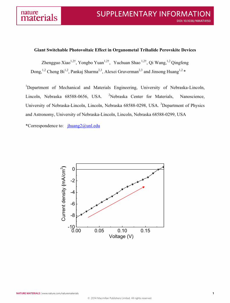
Figure S1. J-V characteristics of the as-prepared vertical structure devices with the structure of
(ITO)/poly(3,4-ethylenedioxythiophene):poly(4-styrenesulfonate) (PEDOT:PSS) /Perovskite (300
nm) /Au. Scanning rate was 0.14 V/s and the scanning direction was labeled in the figure.
Fig. S1 shows current density (J)-voltage (V) characteristics of the as-prepared device with
300 nm perovskite layers. The arrow in the figure depicts the scanning direction. Here, the
scanning direction for J-V characteristics was from zero to positive voltage to rule out the
possibility for a high JSC caused by the un-intentional poling process during device test. It’s
impressive that the device with gold electrode, which usually serves as a contact for hole-only
device, has a high short current density (JSC) of 8.2 mA/cm2. The result indicates the junction has
been partially formed before poling. The reason for junction formation before poling should be
related to different interface structures between perovskite/PEDOT:PSS and perovskite/Au
contacts, because the JSC from the as-fabricated device using gold as both anode and cathode is
much smaller.
3
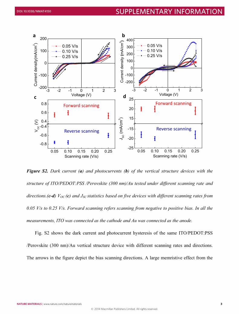
Figure S2. Dark current (a) and photocurrents (b) of the vertical structure devices with the
structure of ITO/PEDOT:PSS /Perovskite (300 nm)/Au tested under different scanning rate and
directions.(c-d) VOC (c) and JSC statistics based on five devices with different scanning rates from
0.05 V/s to 0.25 V/s. Forward scanning refers scanning from negative to positive bias. In all the
measurements, ITO was connected as the cathode and Au was connected as the anode.
Fig. S2 shows the dark current and photocurrent hysteresis of the same ITO/PEDOT:PSS
/Perovskite (300 nm)/Au vertical structure device with different scanning rates and directions.
The arrows in the figure depict the bias scanning directions. A large memristive effect from the
-3 -2 -1 0 1 2 3
-200
-100
0
100
200
300
400 0.05 V/s 0.10 V/s 0.25 V/s
Cur
rent
den
sity
(mA/
cm2 )
Voltage (V)-3 -2 -1 0 1 2 3
-200
-100
0
100
200
C
urre
nt d
ensi
ty(m
A/cm
2 )
Voltage (V)
0.05 V/s 0.10 V/s 0.25 V/s
a b
0.05 0.10 0.15 0.20 0.25
-0.8
-0.6
-0.40.4
0.6
0.8
V OC (V
)
Scanning rate (V/s)0.05 0.10 0.15 0.20 0.25
-25
-20
-15
15
20
25
J SC (m
A/cm
2 )
Scanning rate (V/s)
c d
Forward scanning
Reverse scanning
Forward scanning
Reverse scanning
© 2014 Macmillan Publishers Limited. All rights reserved.
NATURE MATERIALS | www.nature.com/naturematerials 3
SUPPLEMENTARY INFORMATIONDOI: 10.1038/NMAT4150
2
Figure S1. J-V characteristics of the as-prepared vertical structure devices with the structure of
(ITO)/poly(3,4-ethylenedioxythiophene):poly(4-styrenesulfonate) (PEDOT:PSS) /Perovskite (300
nm) /Au. Scanning rate was 0.14 V/s and the scanning direction was labeled in the figure.
Fig. S1 shows current density (J)-voltage (V) characteristics of the as-prepared device with
300 nm perovskite layers. The arrow in the figure depicts the scanning direction. Here, the
scanning direction for J-V characteristics was from zero to positive voltage to rule out the
possibility for a high JSC caused by the un-intentional poling process during device test. It’s
impressive that the device with gold electrode, which usually serves as a contact for hole-only
device, has a high short current density (JSC) of 8.2 mA/cm2. The result indicates the junction has
been partially formed before poling. The reason for junction formation before poling should be
related to different interface structures between perovskite/PEDOT:PSS and perovskite/Au
contacts, because the JSC from the as-fabricated device using gold as both anode and cathode is
much smaller.
3
Figure S2. Dark current (a) and photocurrents (b) of the vertical structure devices with the
structure of ITO/PEDOT:PSS /Perovskite (300 nm)/Au tested under different scanning rate and
directions.(c-d) VOC (c) and JSC statistics based on five devices with different scanning rates from
0.05 V/s to 0.25 V/s. Forward scanning refers scanning from negative to positive bias. In all the
measurements, ITO was connected as the cathode and Au was connected as the anode.
Fig. S2 shows the dark current and photocurrent hysteresis of the same ITO/PEDOT:PSS
/Perovskite (300 nm)/Au vertical structure device with different scanning rates and directions.
The arrows in the figure depict the bias scanning directions. A large memristive effect from the
-3 -2 -1 0 1 2 3
-200
-100
0
100
200
300
400 0.05 V/s 0.10 V/s 0.25 V/s
Cur
rent
den
sity
(mA/
cm2 )
Voltage (V)-3 -2 -1 0 1 2 3
-200
-100
0
100
200
Cur
rent
den
sity
(mA/
cm2 )
Voltage (V)
0.05 V/s 0.10 V/s 0.25 V/s
a b
0.05 0.10 0.15 0.20 0.25
-0.8
-0.6
-0.40.4
0.6
0.8
V OC (V
)
Scanning rate (V/s)0.05 0.10 0.15 0.20 0.25
-25
-20
-15
15
20
25
J SC (m
A/cm
2 )
Scanning rate (V/s)
c d
Forward scanning
Reverse scanning
Forward scanning
Reverse scanning
© 2014 Macmillan Publishers Limited. All rights reserved.
4 NATURE MATERIALS | www.nature.com/naturematerials
SUPPLEMENTARY INFORMATION DOI: 10.1038/NMAT4150
4
devices was observed because the dark- and photocurrent curves have a strong dependence on
the scanning history.
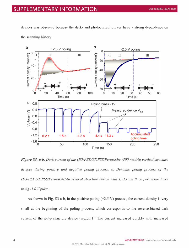
Figure S3. a-b, Dark current of the ITO/PEDOT:PSS/Perovskite (300 nm)/Au vertical structure
devices during positive and negative poling process, c, Dynamic poling process of the
ITO/PEDOT:PSS/Perovskite/Au vertical structure device with 1,015 nm thick perovskite layer
using -1.0 V pulse.
As shown in Fig. S3 a-b, in the positive poling (+2.5 V) process, the current density is very
small at the beginning of the poling process, which corresponds to the reverse-biased dark
current of the n-i-p structure device (region I). The current increased quickly with increased
0 50 100 150 200 250-1.6
-1.2
-0.8
-0.4
0.0
0.4
0.8
Measured device VOC
11.3 s8.4 s4.2 s1.5 s0.2 s
Vol
tage
(V)
Time (s)
Accumulated poling time
Poling bias= -1V
0 20 40 60 80 1000
20
40
60
+2.5 V poling
Cur
rent
den
sity
(mA/
cm2 )
Time (s)0 10 20 30 40 50 60
-80
-60
-40
-20
0
-2.5 V poling
Cur
rent
den
sity
(mA/
cm2 )
Time (s)
a b
- +- + + - + -
c
5
poling time, and a current peak showed up, which should be due to the ion motion in the
perovskite under reverse bias (region II). The current begun to reduce after tens of seconds
poling due to the depletion of easily mobile ions, and the current came to a plateau (region III)
with high current density, indicating the perovskite film was switched to p-i-n structure and the
device worked at forward bias with a large injection current. The negative poling showed a short
poling time than positive poling, indicating the non-symmetrical composition/morphology
profile along the vertical direction.
Fig. S3c shows the dynamic poling process of the device with 1,015 nm thick perovskite
layer. Here a train of -1.0 V pulses with different width were applied on the device, after which
the VOC of the device was measured. The accumulated poling time, poling bias and measured
device VOC were also marked in the figure. As shown in the figure, the device was switched after
11.3 s accumulated poling.
10 100 1000
-1.0
-0.5
0.0
0.5
1.0
JSC (After negative poling) JSC (After positive poling)
Nor
mal
ized
JS
C (a
.u.)
Time (h)
© 2014 Macmillan Publishers Limited. All rights reserved.
NATURE MATERIALS | www.nature.com/naturematerials 5
SUPPLEMENTARY INFORMATIONDOI: 10.1038/NMAT4150
4
devices was observed because the dark- and photocurrent curves have a strong dependence on
the scanning history.
Figure S3. a-b, Dark current of the ITO/PEDOT:PSS/Perovskite (300 nm)/Au vertical structure
devices during positive and negative poling process, c, Dynamic poling process of the
ITO/PEDOT:PSS/Perovskite/Au vertical structure device with 1,015 nm thick perovskite layer
using -1.0 V pulse.
As shown in Fig. S3 a-b, in the positive poling (+2.5 V) process, the current density is very
small at the beginning of the poling process, which corresponds to the reverse-biased dark
current of the n-i-p structure device (region I). The current increased quickly with increased
0 50 100 150 200 250-1.6
-1.2
-0.8
-0.4
0.0
0.4
0.8
Measured device VOC
11.3 s8.4 s4.2 s1.5 s0.2 s
Vol
tage
(V)
Time (s)
Accumulated poling time
Poling bias= -1V
0 20 40 60 80 1000
20
40
60
+2.5 V poling
Cur
rent
den
sity
(mA/
cm2 )
Time (s)0 10 20 30 40 50 60
-80
-60
-40
-20
0
-2.5 V poling
Cur
rent
den
sity
(mA/
cm2 )
Time (s)
a b
- +- + + - + -
c
5
poling time, and a current peak showed up, which should be due to the ion motion in the
perovskite under reverse bias (region II). The current begun to reduce after tens of seconds
poling due to the depletion of easily mobile ions, and the current came to a plateau (region III)
with high current density, indicating the perovskite film was switched to p-i-n structure and the
device worked at forward bias with a large injection current. The negative poling showed a short
poling time than positive poling, indicating the non-symmetrical composition/morphology
profile along the vertical direction.
Fig. S3c shows the dynamic poling process of the device with 1,015 nm thick perovskite
layer. Here a train of -1.0 V pulses with different width were applied on the device, after which
the VOC of the device was measured. The accumulated poling time, poling bias and measured
device VOC were also marked in the figure. As shown in the figure, the device was switched after
11.3 s accumulated poling.
10 100 1000
-1.0
-0.5
0.0
0.5
1.0
JSC (After negative poling) JSC (After positive poling)
Nor
mal
ized
JS
C (a
.u.)
Time (h)
© 2014 Macmillan Publishers Limited. All rights reserved.
6 NATURE MATERIALS | www.nature.com/naturematerials
SUPPLEMENTARY INFORMATION DOI: 10.1038/NMAT4150
6
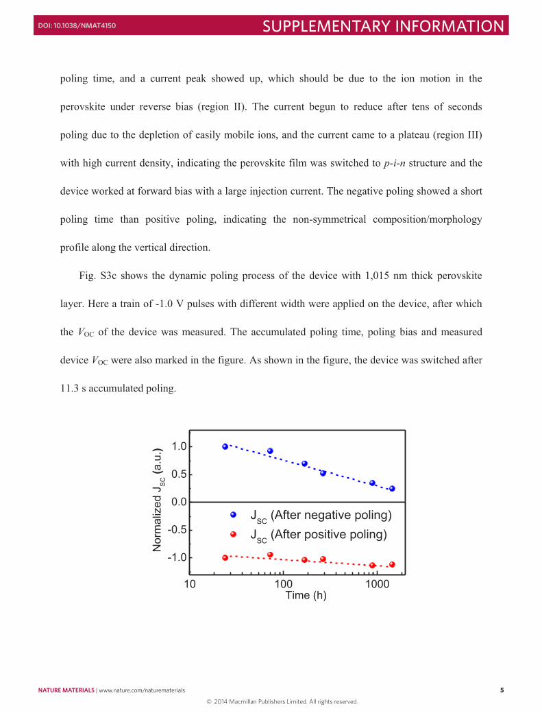
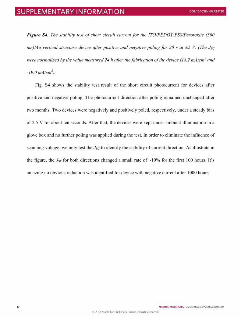
Figure S4. The stability test of short circuit current for the ITO/PEDOT:PSS/Perovskite (300
nm)/Au vertical structure device after positive and negative poling for 20 s at ±2 V. (The JSC
were normalized by the value measured 24 h after the fabrication of the device (18.2 mA/cm2 and
-19.0 mA/cm2).
Fig. S4 shows the stability test result of the short circuit photocurrent for devices after
positive and negative poling. The photocurrent direction after poling remained unchanged after
two months. Two devices were negatively and positively poled, respectively, under a steady bias
of 2.5 V for about ten seconds. After that, the devices were kept under ambient illumination in a
glove box and no further poling was applied during the test. In order to eliminate the influence of
scanning voltage, we only test the JSC to identify the stability of current direction. As illustrate in
the figure, the JSC for both directions changed a small rate of ~10% for the first 100 hours. It’s
amazing no obvious reduction was identified for device with negative current after 1000 hours.
7
Figure S5. Performance variation of the ITO/PEDOT:PSS/Perovskite (300 nm)/Au vertical
structure devices. Scanning rate was 0.14 V/s. Photovoltaic performance statistics of the vertical
structure devices. The vertical structure devices were poled at 6 V/µm for 20 s. The
photocurrents were measured under 1 sun illumination at a sweep rate of 0.14 V/s, b,
Distribution of the photovoltaic performance of vertical structure devices in the JSC-VOC
coordinate. c, VOC distribution of the poled vertical structure devices; d, JSC distribution of the
poled vertical structure device;
It is found that there is a large variation for the performances of the ITO/PEDOT:PSS
/Perovskite (300 nm)/Au vertical structure devices. Some devices showed larger photocurrent
-1.0 -0.5 0.0 0.5 1.0-9
-6
-3
0
3
6
9
12
Positive polingCur
rent
den
sity
(mA
/cm
2 )
Voltage (V)
Negative poling
-1.0 -0.5 0.0 0.5 1.0-20-15-10-505
101520
Positive poling
Negative poling
J SC (
mA
/cm
2 )
VOC (V)
20 10 0 -10 -2001234567
Positive poling
Cou
nt
Negative poling
JSC (mA/cm2)-1.0 -0.5 0.0 0.5 1.002468
1012 Negative poling
C
ount
Positive poling
VOC (V)
a b
dc
© 2014 Macmillan Publishers Limited. All rights reserved.
NATURE MATERIALS | www.nature.com/naturematerials 7
SUPPLEMENTARY INFORMATIONDOI: 10.1038/NMAT4150
6
Figure S4. The stability test of short circuit current for the ITO/PEDOT:PSS/Perovskite (300
nm)/Au vertical structure device after positive and negative poling for 20 s at ±2 V. (The JSC
were normalized by the value measured 24 h after the fabrication of the device (18.2 mA/cm2 and
-19.0 mA/cm2).
Fig. S4 shows the stability test result of the short circuit photocurrent for devices after
positive and negative poling. The photocurrent direction after poling remained unchanged after
two months. Two devices were negatively and positively poled, respectively, under a steady bias
of 2.5 V for about ten seconds. After that, the devices were kept under ambient illumination in a
glove box and no further poling was applied during the test. In order to eliminate the influence of
scanning voltage, we only test the JSC to identify the stability of current direction. As illustrate in
the figure, the JSC for both directions changed a small rate of ~10% for the first 100 hours. It’s
amazing no obvious reduction was identified for device with negative current after 1000 hours.
7
Figure S5. Performance variation of the ITO/PEDOT:PSS/Perovskite (300 nm)/Au vertical
structure devices. Scanning rate was 0.14 V/s. Photovoltaic performance statistics of the vertical
structure devices. The vertical structure devices were poled at 6 V/µm for 20 s. The
photocurrents were measured under 1 sun illumination at a sweep rate of 0.14 V/s, b,
Distribution of the photovoltaic performance of vertical structure devices in the JSC-VOC
coordinate. c, VOC distribution of the poled vertical structure devices; d, JSC distribution of the
poled vertical structure device;
It is found that there is a large variation for the performances of the ITO/PEDOT:PSS
/Perovskite (300 nm)/Au vertical structure devices. Some devices showed larger photocurrent
-1.0 -0.5 0.0 0.5 1.0-9
-6
-3
0
3
6
9
12
Positive polingCur
rent
den
sity
(mA
/cm
2 )
Voltage (V)
Negative poling
-1.0 -0.5 0.0 0.5 1.0-20-15-10-505
101520
Positive poling
Negative poling
J SC (
mA
/cm
2 )
VOC (V)
20 10 0 -10 -2001234567
Positive poling
Cou
nt
Negative poling
JSC (mA/cm2)-1.0 -0.5 0.0 0.5 1.002468
1012 Negative poling
C
ount
Positive poling
VOC (V)
a b
dc
© 2014 Macmillan Publishers Limited. All rights reserved.
8 NATURE MATERIALS | www.nature.com/naturematerials
SUPPLEMENTARY INFORMATION DOI: 10.1038/NMAT4150
8
while some others showed larger VOC. Fig. S5 shows one device with large switchable
photovoltage between 0.87 V and -0.75 V.
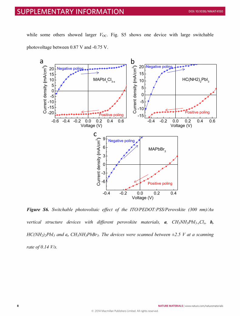
Figure S6. Switchable photovoltaic effect of the ITO/PEDOT:PSS/Perovskite (300 nm)/Au
vertical structure devices with different perovskite materials, a, CH3NH3PbI3-xClx, b,
HC(NH2)2PbI3 and c, CH3NH3PbBr3. The devices were scanned between ±2.5 V at a scanning
rate of 0.14 V/s.
-0.6 -0.4 -0.2 0.0 0.2 0.4 0.6
-20-15-10-505
101520
Positive poling
Negative poling
MAPbIxCl3-x
Cur
rent
den
sity
(mA/
cm2 )
Voltage (V) -0.4 -0.2 0.0 0.2 0.4 0.6
-15-10-505
101520
Positive poling
Negative poling
HC(NH2)2PbI3
Cur
rent
den
sity
(mA/
cm2 )
Voltage (V)
-0.4 -0.2 0.0 0.2 0.4
-6
-3
0
3
6
9
MAPbBr3
Positive poling
Negative poling
Cur
rent
den
sity
(mA/
cm2 )
Voltage (V)
a
c
b
9
In order to confirm the ion drift induced photovoltaic switching mechanism, we examined other
three organolead trihalide perovksite materials, CH3NH3PbI3-xClx, HC(NH2)2PbI3 and
CH3NH3PbBr3 (Fig. S6). It is found all the devices with these materials as active layers showed
field switchable photovoltaic behavior.
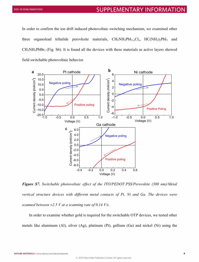
Figure S7. Switchable photovoltaic effect of the ITO/PEDOT:PSS/Perovskite (300 nm)/Metal
vertical structure devices with different metal contacts of Pt, Ni and Ga. The devices were
scanned between ±2.5 V at a scanning rate of 0.14 V/s.
In order to examine whether gold is required for the switchable OTP devices, we tested other
metals like aluminum (Al), silver (Ag), platinum (Pt), gallium (Ga) and nickel (Ni) using the
-1.0 -0.5 0.0 0.5 1.0-20.0-15.0-10.0-5.00.05.0
10.015.020.0
Negative poling
Pt cathode
Positive poling
Cur
rent
den
sity
(mA
/cm
2 )
Voltage (V)-1.0 -0.5 0.0 0.5 1.0
-6
-4
-2
0
2
4
6
Negative poling
Positive Poling
Cur
rent
den
sity
(mA/
cm2 )
Voltage (V)
Ni cathode
-0.4 -0.2 0.0 0.2 0.4 0.6-8.0-6.0-4.0-2.00.02.04.06.0
Negative poling
Ga cathode
Positive poling
Cur
rent
den
sity
(mA
/cm
2 )
Voltage (V)
a b
c
© 2014 Macmillan Publishers Limited. All rights reserved.
NATURE MATERIALS | www.nature.com/naturematerials 9
SUPPLEMENTARY INFORMATIONDOI: 10.1038/NMAT4150
8
while some others showed larger VOC. Fig. S5 shows one device with large switchable
photovoltage between 0.87 V and -0.75 V.
Figure S6. Switchable photovoltaic effect of the ITO/PEDOT:PSS/Perovskite (300 nm)/Au
vertical structure devices with different perovskite materials, a, CH3NH3PbI3-xClx, b,
HC(NH2)2PbI3 and c, CH3NH3PbBr3. The devices were scanned between ±2.5 V at a scanning
rate of 0.14 V/s.
-0.6 -0.4 -0.2 0.0 0.2 0.4 0.6
-20-15-10-505
101520
Positive poling
Negative poling
MAPbIxCl3-x
Cur
rent
den
sity
(mA/
cm2 )
Voltage (V) -0.4 -0.2 0.0 0.2 0.4 0.6
-15-10-505
101520
Positive poling
Negative poling
HC(NH2)2PbI3
Cur
rent
den
sity
(mA/
cm2 )
Voltage (V)
-0.4 -0.2 0.0 0.2 0.4
-6
-3
0
3
6
9
MAPbBr3
Positive poling
Negative poling
Cur
rent
den
sity
(mA/
cm2 )
Voltage (V)
a
c
b
9
In order to confirm the ion drift induced photovoltaic switching mechanism, we examined other
three organolead trihalide perovksite materials, CH3NH3PbI3-xClx, HC(NH2)2PbI3 and
CH3NH3PbBr3 (Fig. S6). It is found all the devices with these materials as active layers showed
field switchable photovoltaic behavior.
Figure S7. Switchable photovoltaic effect of the ITO/PEDOT:PSS/Perovskite (300 nm)/Metal
vertical structure devices with different metal contacts of Pt, Ni and Ga. The devices were
scanned between ±2.5 V at a scanning rate of 0.14 V/s.
In order to examine whether gold is required for the switchable OTP devices, we tested other
metals like aluminum (Al), silver (Ag), platinum (Pt), gallium (Ga) and nickel (Ni) using the
-1.0 -0.5 0.0 0.5 1.0-20.0-15.0-10.0-5.00.05.0
10.015.020.0
Negative poling
Pt cathode
Positive poling
Cur
rent
den
sity
(mA
/cm
2 )
Voltage (V)-1.0 -0.5 0.0 0.5 1.0
-6
-4
-2
0
2
4
6
Negative poling
Positive PolingC
urre
nt d
ensi
ty (m
A/cm
2 )
Voltage (V)
Ni cathode
-0.4 -0.2 0.0 0.2 0.4 0.6-8.0-6.0-4.0-2.00.02.04.06.0
Negative poling
Ga cathode
Positive poling
Cur
rent
den
sity
(mA
/cm
2 )
Voltage (V)
a b
c
© 2014 Macmillan Publishers Limited. All rights reserved.
10 NATURE MATERIALS | www.nature.com/naturematerials
SUPPLEMENTARY INFORMATION DOI: 10.1038/NMAT4150
10
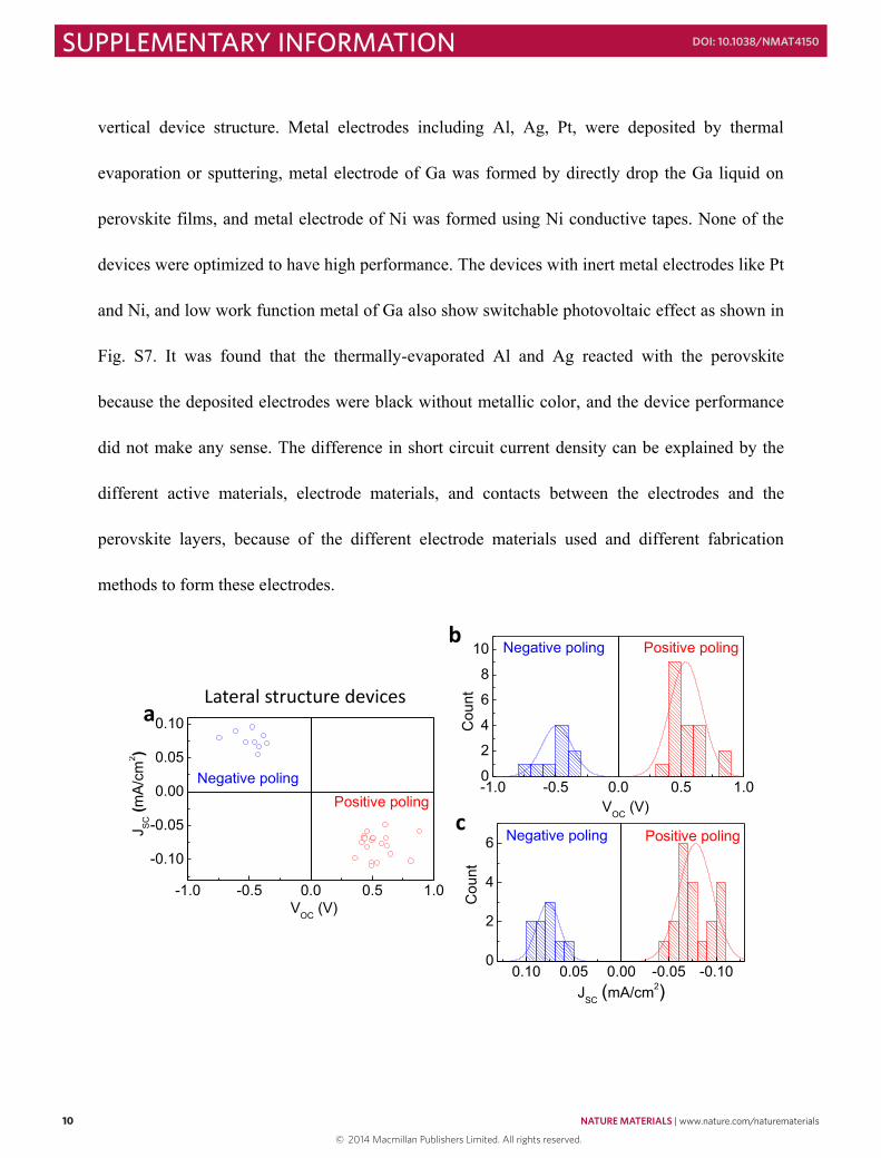
vertical device structure. Metal electrodes including Al, Ag, Pt, were deposited by thermal
evaporation or sputtering, metal electrode of Ga was formed by directly drop the Ga liquid on
perovskite films, and metal electrode of Ni was formed using Ni conductive tapes. None of the
devices were optimized to have high performance. The devices with inert metal electrodes like Pt
and Ni, and low work function metal of Ga also show switchable photovoltaic effect as shown in
Fig. S7. It was found that the thermally-evaporated Al and Ag reacted with the perovskite
because the deposited electrodes were black without metallic color, and the device performance
did not make any sense. The difference in short circuit current density can be explained by the
different active materials, electrode materials, and contacts between the electrodes and the
perovskite layers, because of the different electrode materials used and different fabrication
methods to form these electrodes.
-1.0 -0.5 0.0 0.5 1.0
-0.10
-0.05
0.00
0.05
0.10
Positive polingNegative poling
J SC (m
A/c
m2 )
VOC (V)
0.10 0.05 0.00 -0.05 -0.100
2
4
6 Positive poling
Cou
nt
Negative poling
JSC (mA/cm2)
-1.0 -0.5 0.0 0.5 1.00
2
4
6
8
10 Negative poling
C
ount
Positive poling
VOC (V)
Lateral structure devicesa
b
c
11
Figure S8. Photovoltaic performance statistics of the lateral structure devices. The lateral
structure devices were poled under 1.2 V/µm for 100 s, and photocurrent were measured under a
quarter sun illumination with a sweep rate of 0.05 V/s. a, distribution of the photovoltaic
performance of lateral structure devices in the JSC-VOC coordinate. b, VOC distribution of the
poled lateral structure devices; c, JSC distribution of the poled lateral structure devices.
Figure S9. J-V characteristics of the Au/perovskite (300 nm)/Au lateral structure devices with
different electrode spacing. The devices were poled under 1.2 V/µm for 100 s, and photocurrent
were measured under a quarter sun illumination with a sweep rate of 0.05 V/s.
Fig. S9 shows the normalized photocurrent curves with respect to the electrode spacing in
the Au/perovskite/Au lateral structure devices. In contrast to ferroelectric photovoltaic devices
10-410-310-210-1100
d=8 m
10-2
10-1
100
d=50 m
Nor
mal
ized
J(a
.u.)
-1.0 -0.5 0.0 0.5 1.0 1.5 2.010-2
10-1
100
d=100 m
Voltage (V)
© 2014 Macmillan Publishers Limited. All rights reserved.

NATURE MATERIALS | www.nature.com/naturematerials 11
SUPPLEMENTARY INFORMATIONDOI: 10.1038/NMAT4150
10
vertical device structure. Metal electrodes including Al, Ag, Pt, were deposited by thermal
evaporation or sputtering, metal electrode of Ga was formed by directly drop the Ga liquid on
perovskite films, and metal electrode of Ni was formed using Ni conductive tapes. None of the
devices were optimized to have high performance. The devices with inert metal electrodes like Pt
and Ni, and low work function metal of Ga also show switchable photovoltaic effect as shown in
Fig. S7. It was found that the thermally-evaporated Al and Ag reacted with the perovskite
because the deposited electrodes were black without metallic color, and the device performance
did not make any sense. The difference in short circuit current density can be explained by the
different active materials, electrode materials, and contacts between the electrodes and the
perovskite layers, because of the different electrode materials used and different fabrication
methods to form these electrodes.
-1.0 -0.5 0.0 0.5 1.0
-0.10
-0.05
0.00
0.05
0.10
Positive polingNegative poling
J SC (m
A/c
m2 )
VOC (V)
0.10 0.05 0.00 -0.05 -0.100
2
4
6 Positive poling
Cou
nt
Negative poling
JSC (mA/cm2)
-1.0 -0.5 0.0 0.5 1.00
2
4
6
8
10 Negative poling
C
ount
Positive poling
VOC (V)
Lateral structure devicesa
b
c
11
Figure S8. Photovoltaic performance statistics of the lateral structure devices. The lateral
structure devices were poled under 1.2 V/µm for 100 s, and photocurrent were measured under a
quarter sun illumination with a sweep rate of 0.05 V/s. a, distribution of the photovoltaic
performance of lateral structure devices in the JSC-VOC coordinate. b, VOC distribution of the
poled lateral structure devices; c, JSC distribution of the poled lateral structure devices.
Figure S9. J-V characteristics of the Au/perovskite (300 nm)/Au lateral structure devices with
different electrode spacing. The devices were poled under 1.2 V/µm for 100 s, and photocurrent
were measured under a quarter sun illumination with a sweep rate of 0.05 V/s.
Fig. S9 shows the normalized photocurrent curves with respect to the electrode spacing in
the Au/perovskite/Au lateral structure devices. In contrast to ferroelectric photovoltaic devices
10-410-310-210-1100
d=8 m
10-2
10-1
100
d=50 m
Nor
mal
ized
J(a
.u.)
-1.0 -0.5 0.0 0.5 1.0 1.5 2.010-2
10-1
100
d=100 m
Voltage (V)
© 2014 Macmillan Publishers Limited. All rights reserved.
12 NATURE MATERIALS | www.nature.com/naturematerials
SUPPLEMENTARY INFORMATION DOI: 10.1038/NMAT4150
12
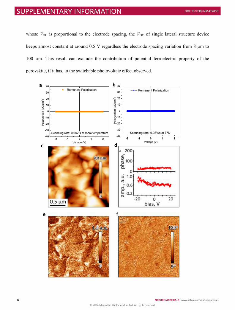
whose VOC is proportional to the electrode spacing, the VOC of single lateral structure device
keeps almost constant at around 0.5 V regardless the electrode spacing variation from 8 µm to
100 µm. This result can exclude the contribution of potential ferroelectric property of the
perovskite, if it has, to the switchable photovoltaic effect observed.
-2 -1 0 1 2-40
-30
-20
-10
0
10
20
30
40
Remanent Polarization
Scanning rate: 0.08V/s at room temperature
Pol
ariz
atio
n (
C/c
m2 )
Voltage (V)-2 -1 0 1 2
-40
-30
-20
-10
0
10
20
30
40
Remanent Polarization
Scanning rate: 0.08V/s at 77K
Pol
ariz
atio
n (
C/c
m2 )
Voltage (V)
a b
c d
e f
13
Figure S10. Ferroelectric polarization loops measured at room temperature (a) and at 77 K (b)
scanned at the same frequency of photovoltaic switch process. c, Piezoresponse force
microscopy (PFM) topology (c), amplitude (e) and phase (f) images of the perovskite (300 nm). d,
Representative PFM hysteresis loops (phase and amplitude) signal for any location on the film
surface.
Theoretical calculation predicted ferroelectric property of MAPbI3 with spontaneous
polarization of 38 µC/cm2 (1). We measured the ferroelectric hysteresis using the Precision
Premier Ⅱ from the Radiant technologies, Inc.. However we did not find any ferroelectric
polarization within the measurement range of the equipment from these devices both at room
temperature and at 77 K and using the same frequency of photovoltaic switch process. This
results further exclude the contribution of potential ferroelectric property of the perovskite, if it
has, to the switchable photovoltaic effect observed.
© 2014 Macmillan Publishers Limited. All rights reserved.

NATURE MATERIALS | www.nature.com/naturematerials 13
SUPPLEMENTARY INFORMATIONDOI: 10.1038/NMAT4150
12
whose VOC is proportional to the electrode spacing, the VOC of single lateral structure device
keeps almost constant at around 0.5 V regardless the electrode spacing variation from 8 µm to
100 µm. This result can exclude the contribution of potential ferroelectric property of the
perovskite, if it has, to the switchable photovoltaic effect observed.
-2 -1 0 1 2-40
-30
-20
-10
0
10
20
30
40
Remanent Polarization
Scanning rate: 0.08V/s at room temperature
Pol
ariz
atio
n (
C/c
m2 )
Voltage (V)-2 -1 0 1 2
-40
-30
-20
-10
0
10
20
30
40
Remanent Polarization
Scanning rate: 0.08V/s at 77K
Pol
ariz
atio
n (
C/c
m2 )
Voltage (V)
a b
c d
e f
13
Figure S10. Ferroelectric polarization loops measured at room temperature (a) and at 77 K (b)
scanned at the same frequency of photovoltaic switch process. c, Piezoresponse force
microscopy (PFM) topology (c), amplitude (e) and phase (f) images of the perovskite (300 nm). d,
Representative PFM hysteresis loops (phase and amplitude) signal for any location on the film
surface.
Theoretical calculation predicted ferroelectric property of MAPbI3 with spontaneous
polarization of 38 µC/cm2 (1). We measured the ferroelectric hysteresis using the Precision
Premier Ⅱ from the Radiant technologies, Inc.. However we did not find any ferroelectric
polarization within the measurement range of the equipment from these devices both at room
temperature and at 77 K and using the same frequency of photovoltaic switch process. This
results further exclude the contribution of potential ferroelectric property of the perovskite, if it
has, to the switchable photovoltaic effect observed.
© 2014 Macmillan Publishers Limited. All rights reserved.
14 NATURE MATERIALS | www.nature.com/naturematerials
SUPPLEMENTARY INFORMATION DOI: 10.1038/NMAT4150
14
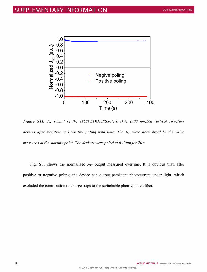
Figure S11. JSC output of the ITO/PEDOT:PSS/Perovskite (300 nm)/Au vertical structure
devices after negative and positive poling with time. The JSC were normalized by the value
measured at the starting point. The devices were poled at 6 V/µm for 20 s.
Fig. S11 shows the normalized JSC output measured overtime. It is obvious that, after
positive or negative poling, the device can output persistent photocurrent under light, which
excluded the contribution of charge traps to the switchable photovoltaic effect.
0 100 200 300 400-1.0-0.8-0.6-0.4-0.20.00.20.40.60.81.0
Negive poling Positive poling
Nor
mal
ized
JS
C (a
.u.)
Time (s)
15
Figure S12. AFM topography image (a), surface potential image (c) and adhesion image (d) of
the perovskite film after positive poling. AFM topography image of another film after negative
poling (b).
The Au electrode in topography image shown in Fig. S12 is not clear because the thickness of
the Au electrode is only about 50 nm, much smaller than the roughness (~150 nm) of the
perovskite thin films formed on glass. Nevertheless, we observed a clear difference of Au region
and perovskite region as well as the separation line between these two regions by examining the
adhesion mapping recorded during AFM scanning. The adhesion mapping of the exact same area
of Fig. 3e is shown in Fig. S12d. Adhesion is defined as the minimum tension (“pull-off”) forces
134.6 nm
-111.6 nm
102.1 nm
-95.4 nm
+ polingperovskite
Au
- polingperovskite
Au
a b
c d+ polingperovskite
+ polingperovskite
© 2014 Macmillan Publishers Limited. All rights reserved.

NATURE MATERIALS | www.nature.com/naturematerials 15
SUPPLEMENTARY INFORMATIONDOI: 10.1038/NMAT4150
14
Figure S11. JSC output of the ITO/PEDOT:PSS/Perovskite (300 nm)/Au vertical structure
devices after negative and positive poling with time. The JSC were normalized by the value
measured at the starting point. The devices were poled at 6 V/µm for 20 s.
Fig. S11 shows the normalized JSC output measured overtime. It is obvious that, after
positive or negative poling, the device can output persistent photocurrent under light, which
excluded the contribution of charge traps to the switchable photovoltaic effect.
0 100 200 300 400-1.0-0.8-0.6-0.4-0.20.00.20.40.60.81.0
Negive poling Positive poling
Nor
mal
ized
JS
C (a
.u.)
Time (s)
15
Figure S12. AFM topography image (a), surface potential image (c) and adhesion image (d) of
the perovskite film after positive poling. AFM topography image of another film after negative
poling (b).
The Au electrode in topography image shown in Fig. S12 is not clear because the thickness of
the Au electrode is only about 50 nm, much smaller than the roughness (~150 nm) of the
perovskite thin films formed on glass. Nevertheless, we observed a clear difference of Au region
and perovskite region as well as the separation line between these two regions by examining the
adhesion mapping recorded during AFM scanning. The adhesion mapping of the exact same area
of Fig. 3e is shown in Fig. S12d. Adhesion is defined as the minimum tension (“pull-off”) forces
134.6 nm
-111.6 nm
102.1 nm
-95.4 nm
+ polingperovskite
Au
- polingperovskite
Au
a b
c d+ polingperovskite
+ polingperovskite
© 2014 Macmillan Publishers Limited. All rights reserved.

16 NATURE MATERIALS | www.nature.com/naturematerials
SUPPLEMENTARY INFORMATION DOI: 10.1038/NMAT4150
16
required for retracting the AFM tip from the sample surface. Many different types of interaction
forces, mainly van der Waals and/or electrostatic force, attribute to adhesion. Because the
interaction between tips with different materials have different adhesion, which constitutes the
contrast, this technology has been applied to a wide variety of materials to investigate the surface
heterogeneity or material distributions. As shown in Fig. 3e and Fig. S12d, the adhesion mapping
agrees well with the KPFM mapping.
Figure S13. A SEM image of a Au/perovskite/Au lateral structure device after poling
It shows the morphology change of perovskite after poling near the anode area. Compared
to the area far away from the anode, the area close to the Au electrode showed a lot of pin-holes
formed.
17
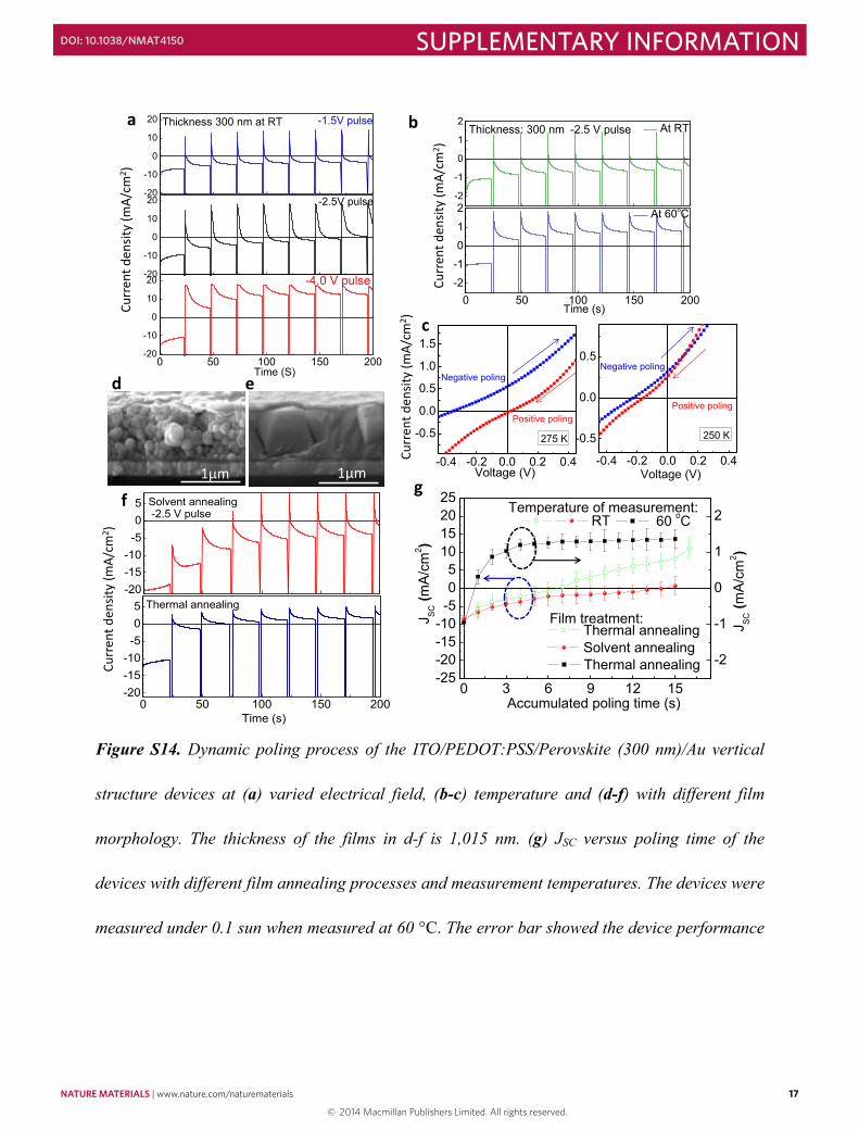
Figure S14. Dynamic poling process of the ITO/PEDOT:PSS/Perovskite (300 nm)/Au vertical
structure devices at (a) varied electrical field, (b-c) temperature and (d-f) with different film
morphology. The thickness of the films in d-f is 1,015 nm. (g) JSC versus poling time of the
devices with different film annealing processes and measurement temperatures. The devices were
measured under 0.1 sun when measured at 60 °C. The error bar showed the device performance
0 3 6 9 12 15-25-20-15-10-505
10152025
Temperature of measurement:
Film treatment:
RT
Thermal annealing Solvent annealing
J SC (m
A/cm
2 )
J SC (m
A/cm
2 )
Accumulated poling time (s)
-2
-1
0
1
2 60 oC
Thermal annealing
-20
-10
0
10
20 -1.5V pulseThickness 300 nm at RT
0 50 100 150 200-20
-10
0
10
20 -4.0 V pulse
Time (S)
-20
-10
0
10
20 -2.5V pulse
Curr
ent d
ensit
y (m
A/cm
2 )
-2
-1
0
1
2-2.5 V pulse At RT Thickness: 300 nm
0 50 100 150 200-2-1012 At 60oC
Time (s)
Curr
ent d
ensit
y (m
A/cm
2 )
a b
0 50 100 150 200-20-15-10
-505 Thermal annealing
Time (s)
-20-15-10
-505
-2.5 V pulseSolvent annealing
d e
1µm 1µm
f
Curr
ent d
ensit
y (m
A/cm
2 )
c
Curr
ent d
ensit
y (m
A/cm
2 )
-0.4 -0.2 0.0 0.2 0.4
-0.5
0.0
0.5
1.0
1.5
Voltage (V)
Positive poling
275 K
Negative poling
-0.4 -0.2 0.0 0.2 0.4
-0.5
0.0
0.5
Positive poling
250 K
Voltage (V)
Negative poling
g
© 2014 Macmillan Publishers Limited. All rights reserved.
NATURE MATERIALS | www.nature.com/naturematerials 17
SUPPLEMENTARY INFORMATIONDOI: 10.1038/NMAT4150
16
required for retracting the AFM tip from the sample surface. Many different types of interaction
forces, mainly van der Waals and/or electrostatic force, attribute to adhesion. Because the
interaction between tips with different materials have different adhesion, which constitutes the
contrast, this technology has been applied to a wide variety of materials to investigate the surface
heterogeneity or material distributions. As shown in Fig. 3e and Fig. S12d, the adhesion mapping
agrees well with the KPFM mapping.
Figure S13. A SEM image of a Au/perovskite/Au lateral structure device after poling
It shows the morphology change of perovskite after poling near the anode area. Compared
to the area far away from the anode, the area close to the Au electrode showed a lot of pin-holes
formed.
17
Figure S14. Dynamic poling process of the ITO/PEDOT:PSS/Perovskite (300 nm)/Au vertical
structure devices at (a) varied electrical field, (b-c) temperature and (d-f) with different film
morphology. The thickness of the films in d-f is 1,015 nm. (g) JSC versus poling time of the
devices with different film annealing processes and measurement temperatures. The devices were
measured under 0.1 sun when measured at 60 °C. The error bar showed the device performance
0 3 6 9 12 15-25-20-15-10-505
10152025
Temperature of measurement:
Film treatment:
RT
Thermal annealing Solvent annealing
J SC (m
A/cm
2 )
J SC (m
A/cm
2 )
Accumulated poling time (s)
-2
-1
0
1
2 60 oC
Thermal annealing
-20
-10
0
10
20 -1.5V pulseThickness 300 nm at RT
0 50 100 150 200-20
-10
0
10
20 -4.0 V pulse
Time (S)
-20
-10
0
10
20 -2.5V pulse
Curr
ent d
ensit
y (m
A/cm
2 )
-2
-1
0
1
2-2.5 V pulse At RT Thickness: 300 nm
0 50 100 150 200-2-1012 At 60oC
Time (s)
Curr
ent d
ensit
y (m
A/cm
2 )
a b
0 50 100 150 200-20-15-10
-505 Thermal annealing
Time (s)
-20-15-10
-505
-2.5 V pulseSolvent annealing
d e
1µm 1µm
f
Curr
ent d
ensit
y (m
A/cm
2 )
c
Curr
ent d
ensit
y (m
A/cm
2 )
-0.4 -0.2 0.0 0.2 0.4
-0.5
0.0
0.5
1.0
1.5
Voltage (V)
Positive poling
275 K
Negative poling
-0.4 -0.2 0.0 0.2 0.4
-0.5
0.0
0.5
Positive poling
250 K
Voltage (V)
Negative poling
g
© 2014 Macmillan Publishers Limited. All rights reserved.
18 NATURE MATERIALS | www.nature.com/naturematerials
SUPPLEMENTARY INFORMATION DOI: 10.1038/NMAT4150
18
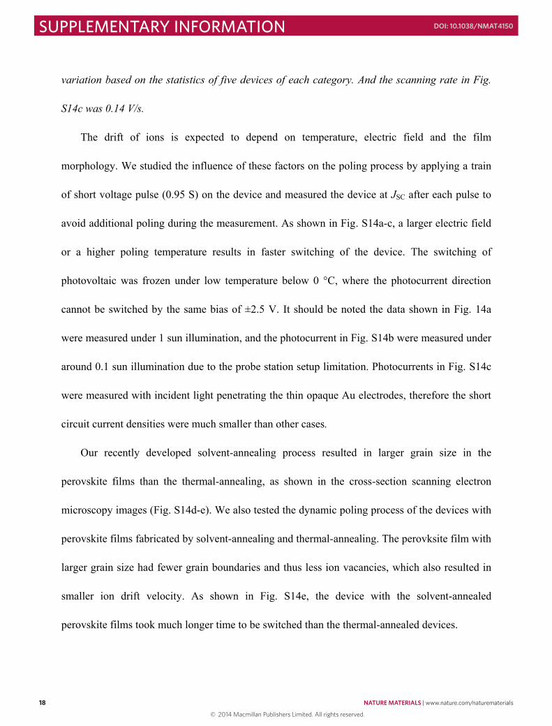
variation based on the statistics of five devices of each category. And the scanning rate in Fig.
S14c was 0.14 V/s.
The drift of ions is expected to depend on temperature, electric field and the film
morphology. We studied the influence of these factors on the poling process by applying a train
of short voltage pulse (0.95 S) on the device and measured the device at JSC after each pulse to
avoid additional poling during the measurement. As shown in Fig. S14a-c, a larger electric field
or a higher poling temperature results in faster switching of the device. The switching of
photovoltaic was frozen under low temperature below 0 °C, where the photocurrent direction
cannot be switched by the same bias of ±2.5 V. It should be noted the data shown in Fig. 14a
were measured under 1 sun illumination, and the photocurrent in Fig. S14b were measured under
around 0.1 sun illumination due to the probe station setup limitation. Photocurrents in Fig. S14c
were measured with incident light penetrating the thin opaque Au electrodes, therefore the short
circuit current densities were much smaller than other cases.
Our recently developed solvent-annealing process resulted in larger grain size in the
perovskite films than the thermal-annealing, as shown in the cross-section scanning electron
microscopy images (Fig. S14d-e). We also tested the dynamic poling process of the devices with
perovskite films fabricated by solvent-annealing and thermal-annealing. The perovksite film with
larger grain size had fewer grain boundaries and thus less ion vacancies, which also resulted in
smaller ion drift velocity. As shown in Fig. S14e, the device with the solvent-annealed
perovskite films took much longer time to be switched than the thermal-annealed devices.
© 2014 Macmillan Publishers Limited. All rights reserved.