supplementary information - nature · the second thiol-dosed data set of fig 1 (right) minus the...
TRANSCRIPT
Differential stress induced by thiol adsorption on facetted nanocrystals (Supplementary Information)
Moyu Watari, Rachel McKendry, Manuel Vögtli, Gabriel Aeppli, Yeong-Ah Soh, Xiaowen Shi, Gang Xiong, Xiaojing Huang, Ross Harder and
Ian Robinson London Centre for Nanotechnology
I Sensitivity of Difference Fourier Map to Origin of Data
An obvious approach to analysing the structural changes due to thiol adsorption would be to invert the diffraction patterns of both the bare and dosed crystals, then compare the differences. However, the direct comparison between such images is made very difficult because of symmetries in the Fourier transform: even with a tight support and limited real-space phase range, the solution is insensitive to arbitrary rigid-body translations and phase offsets. In practice, the image emerges roughly at the centre of the support box and phase range, but the exact choice is very sensitive to noise in the data, and can vary with the different random starting phases used to seed the phasing algorithm [15]. So we have used the difference Fourier map (DFM) method instead, as described in the main paper. The widespread use of the DFM method in crystallography is justified in ref [19] and other papers. The intuitive arguments are independent of resolution, so apply to Coherent Diffraction Imaging as well. The DFM applies to the situation where the structural changes are localised in real space, meaning confined to a small fraction of the sample volume, which is certainly appropriate here. The consequence in reciprocal space is a widely distributed small change in all structure factors; the average amount of change is approximately the fraction of the real-space volume that is modified, less than 1% here. In Fig 1, it can be seen that the intensity changes are widely distributed, even though they are small. A small change in the real and imaginary parts of a structure factor shows up mainly in the magnitude of the structure factor and only slightly in its phase. So the error in the structure associated with keeping the original phase is the cosine of this small change, which is only second order. The data in Fig 1 were normalized to the value of the highest intensity pixel. Any error in normalisation would show up as a background ghost image of the nanoparticle itself in the DFM, which is real. As explained in the main text, the differences due to strain show up in the imaginary part of the image and so are orthogonal and quite easy to distinguish. The definition of q presents the problem that the point chosen to be the 3D centre of the diffraction pattern, for example in Fig 1, needs to be chosen very carefully. Even a single pixel error in the choice of G will lead to an artificial structure difference in Δρ(r). It is straightforward to show that the resulting image will be the spatial derivative of the crystal density, ρ(r), along the direction of the error. Despite our considerable efforts to minimise the variations in alignment from one scan to the next, the outcome was typically only stable to about one pixel of the CCD and occasionally worse, believed to come from tiny angular sample motions and instrument instability. The dataset shown in Fig 1 and used for the subsequent analysis was a particularly stable example. The highest intensity pixel, taken to be the point where Q = G, was the same for all three datasets shown. The effect of single-pixel variations in the choice of
SUPPLEMENTARY INFORMATIONDOI: 10.1038/NMAT3124
NATURE MATERIALS | www.nature.com/naturematerials 1
© 2011 Macmillan Publishers Limited. All rights reserved.
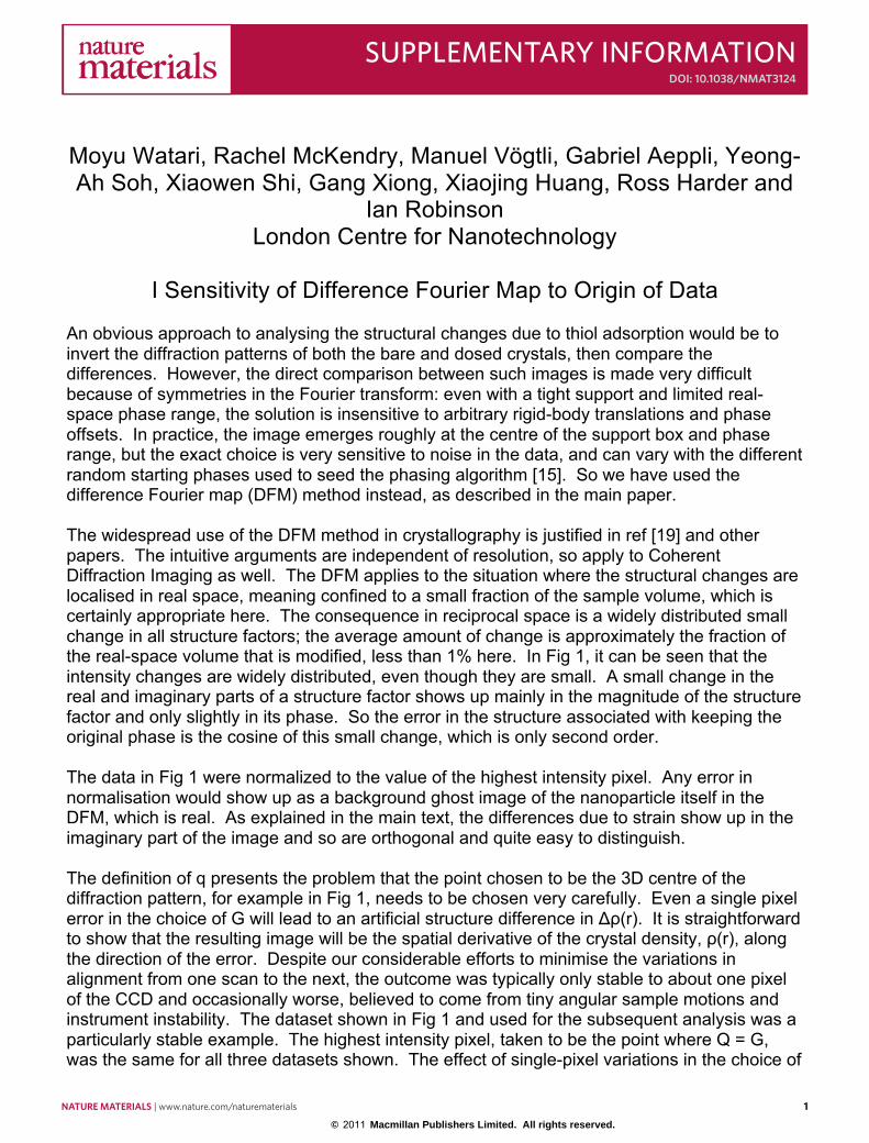
centering is shown in Fig S1. All panels show 50% isosurface images of Δρ(r) for data shifts in various directions. The correct centering of the middle panel leads to a (smaller) rounded difference peak, which follows the direction of the G-vector, whereas all misalignments lead to dumbbell-shaped peaks following the direction of the axis used.
Figure S1. Effect of data-centering errors in evaluation of the difference Fourier map for the second thiol-dosed data set of Fig 1 (right) minus the undosed Fig 1 (left). The effect of single-pixel errors along the x-axis (horizontal detector direction) and z-axis (diffraction angle) are shown.
We are interested in the very small phase changes caused by strain difference before and after thiol absorption. It is also well-known that if the centers of diffraction patterns are misaligned with each other, a relative phase ramp will be introduced in obtained real space images. These two phase differences will combine together in the output of the difference Fourier calculation. To eliminate the effect from misalignment of diffraction patterns, we used a sub-pixel registration method [S1] to align diffraction centers with an accuracy of 0.01 pixel. Considering a pair of 2D (Nx, Ny) arrays, the sub-pixel registration process was processed in two steps. In the first step, both arrays were upscaled by a factor of 2, and the cross correlation peak indicates the misalignment value with 0.5 pixel accuracy. To achieve 1/k pixel alignment accuracy, the arrays have to be upscaled by k-fold in each dimension, which becomes inefficient when approaching higher precisions. Instead, in the second step, only a small region (1.5x1.5 pixel) surrounding the peak found in the first step is upscaled to a factor of k using matrix-multiple Discrete Fourier Transform (DFT) approach [S2]. The cross-correlation peak of the obtained arrays gives refined shifting value with an accuracy of 1/k pixel.
2 NATURE MATERIALS | www.nature.com/naturematerials
SUPPLEMENTARY INFORMATION DOI: 10.1038/NMAT3124
© 2011 Macmillan Publishers Limited. All rights reserved.

To extend this method to align 3D diffraction patterns, we took the 2D central slices in (X, Y), (X, Z) and (Y, Z) planes. These planes correspond to the 2D projection images in real space. By aligning each plane pair with the same accuracy, two shifted values were obtained in each direction, which were averaged to give the final shifting value. To correct the misalignment, one of the diffraction patterns was inverse Fourier transformed, multiplied by a linear phase ramp determined by the shifted pixel number, and then Fourier transformed back to real space. The sub-pixel registration and alignment processes were repeated until no more correction is needed. This method was applied to the data sets of Fig 1 and the sub-pixel corrected difference density was found not to be significantly changed from the nearest-integer (unbinned) pixel alignment shown in Fig S1.
II Self Assembled Monolayers (SAMs) on polycrystal Au
Within the ‘staple’ structures seen in the crystallographic structure [2] the sulphur atoms are embedded within a mixed Au-S layer, while their organic ligands are retained. These can form a sound anchoring mechanism for the SAM, but the required disruption to the gold substrate, expelling an adatom, would tend to disfavour SAM formation on classical close-packed low-index surfaces [10]. In the case of a polycrystalline film on a cantilever, there is also the long-range averaging, not only over the grain morphologies and any facets that might present themselves, but also over the contacts between grains that are assumed not to change when the thiol SAM is formed [23]. The question of thiol penetration of the grain boundaries and even undercutting the film is similarly not discussed; here we see a comparable strain on the (11-1) and (-1-11) directions suggesting that the SAM wraps fully around the particle. Propagation of stress from one grain to another within the macroscopic film and extending over the variations in morphology has been discussed by some of the authors of the cantilever work [23] and is certainly important to the mechanical transmission process. A strong grain size effect was found, with more than an order of magnitude increase of cantilever stress with size [24]. The boundaries between the grains of the polycrystalline films are likely to be significantly influenced by the growth temperature and evaporation rate of the films (as used to adjust the grain size) as well as the subsequent treatment. Therefore the relevance of microscopic strain reported here, measured on individual, isolated Au nanocrystals, has to be modelled carefully in the description of the resulting macroscopic behaviour of a polycrystalline film. The exact distribution and morphology of a SAM upon a percolating network of contacted grains, and how this contributes to stress generation, is a challenging research question waiting to be tackled.
III Equilibrium Crystal Shapes As formed by dewetting a film from a silicon wafer substrate (see detailed methods below), the shape of our nanocrystals is found to be spherical with {111} facets, as expected from the theory of Equilibrium Crystal Shapes (ECS) [17]. Especially on a nanocrystal, where the surface region is a significant fraction of the entire sample, the flat facets of the crystal become differentially contracted relative to its spherical regions owing to a different level of surface stress present. This is seen in Fig S2 as a residual strain in the as-formed nanocrystals, which
NATURE MATERIALS | www.nature.com/naturematerials 3
SUPPLEMENTARY INFORMATIONDOI: 10.1038/NMAT3124
© 2011 Macmillan Publishers Limited. All rights reserved.

is found to be slightly different for every one. Since the thiol dosing measurements are fully quantitative, we are still able to obtain reliable numbers for the strain changes caused by the adsorption, even in the presence of these initial strains.
Figure S2. Phase-coloured isosurface of one of the Au nanocrystals, as prepared by dewtting from an evaporated film. The range of phases shown is from -1 radian (blue) to +1 radian (red), corresponding to ±0.04nm displacement along (11-1) from the average crystal lattice. Residual strains can be clearly seen. This, along with the fact that the aspect ratio is still flattened, shows the limited extent to which the ECS has been reached by our preparation procedure. All eight {111} facet directions are indicated with arrows.
Although CXD sees the full 3D bulk of the sample, it is still sensitive to surface strains. This was seen in a Pb nanocrystal close to its melting point [14]. In that work, a {111} facet of the ECS was found to have a smaller component of inward lattice displacement than the neighbouring curved regions of the crystal surface. Even with the limited spatial resolution of CXD, the surface strain can be visualised when it is associated with a sufficiently extended object, such as a crystal facet; the strain, obeying a Poisson relationship, decays on a length scale comparable in extent with the size of the object. According to theory [17], the curved (approximately spherical) regions of an ECS are thermodynamically rough with a dynamic equilibrium of microscopic surface steps in continual motion [S3], while the facets are static structures following low-index crystallographic directions, {111} in this case. So for Au at ambient temperature, the slow kinetics seen may be related to the involvement of step diffusion in the formation of Au-thiol complexes.
IV Sign Conventions The definition and sign of surface stress is explained in the reviews by Haiss [26] and Ibach [27]. The definition of surface stress, , is given by the Shuttleworth equation as a strain derivative of the surface energy with an additional offset contribution from the surface energy (which defines the zero),
4 NATURE MATERIALS | www.nature.com/naturematerials
SUPPLEMENTARY INFORMATION DOI: 10.1038/NMAT3124
© 2011 Macmillan Publishers Limited. All rights reserved.

Here is the surface energy, is the strain and is the Kronecker delta symbol. When , the surface energy, is lowered for negative strain values, (ie when the surface spacings are allowed to shrink) then the change in surface stress is positive. This is the situation for most clean metal surfaces where the interatomic attractions are greater between neighbours than in the bulk [26]. Such surfaces have positive stress and tend to undergo inwards relaxation in their structures. The Shuttleworth equation defines the sign of the surface stress, . In the situation above, the positive stress is called ‘tensile’. If the surface tends to expand to lower the energy, the corresponding stress change has a negative sign and is called ‘compressive’. Suppose a cantilever has a gold coating on its upper surface, which is subsequently exposed to a thiol SAM. If the cantilever bends upwards upon exposure, bending towards the thiol, the gold atoms of its surface are contracting by moving together. This indicates a positive, tensile change of surface stress in the gold film. Conversely, a downward deflection away from the coated side, indicates a negative, compressive change of stress in the surface of the gold film. The widely-cited thiol cantilever Science paper of Berger et al [23], reported an unexpected bending away from the thiol-coated side of the cantilever. It was correctly stated that this implies a compressive stress, however, the stress change measurements were given with positive signs, not following the convention above. The sign convention was also not followed in the measured stress curves of the Langmuir paper of Godin et al [24], but the stresses were correctly indicated with a negative sign in their later Nanotechnology paper [25]. In this paper we have corrected the signs to quote all stresses as belonging to the surface of the metal substrate, following the convention of the Shuttleworth equation, whereby mechanical expansions in the surface of the metal film follow from compressive stress with a negative change of , denoted .
V Cantilever Measurements Because cantilever bending results for propane thiol (C3H7SH) had not been reported before and because of uncertainties in the literature about the chain-length dependence of the stress caused by thiol binding on gold films, we made our own cantilever measurements for propane thiol (C3H7SH) and dodecane thiol (C12H25SH) binding. When a drop of 5 mM propane thiol (C3H7SH) solution in ethanol was introduced (see methods), the gold-coated cantilevers began bending upwards, reaching a tensile surface stress of 150 mN/m, as shown in the time course of Fig. S3. After the addition of a drop of pure propane thiol, the stress increased to 240 mN/m. The higher deflection for pure thiol can be explained by a higher vapour concentration of the thiol. Reference uncoated silicon cantilevers did not reveal any significant bending, suggesting that the response is entirely due to thiol binding specifically to the gold substrate.
NATURE MATERIALS | www.nature.com/naturematerials 5
SUPPLEMENTARY INFORMATIONDOI: 10.1038/NMAT3124
© 2011 Macmillan Publishers Limited. All rights reserved.
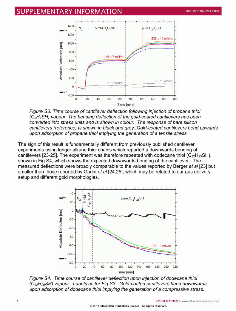
Figure S3: Time course of cantilever deflection following injection of propane thiol (C3H7SH) vapour. The bending deflection of the gold-coated cantilevers has been converted into stress units and is shown in colour. The response of bare silicon cantilevers (reference) is shown in black and grey. Gold-coated cantilevers bend upwards upon adsorption of propane thiol implying the generation of a tensile stress.
The sign of this result is fundamentally different from previously published cantilever experiments using longer alkane thiol chains which reported a downwards bending of cantilevers [23-25]. The experiment was therefore repeated with dodecane thiol (C12H25SH), shown in Fig S4, which shows the expected downwards bending of the cantilever. The measured deflections were broadly comparable to the values reported by Berger et al [23] but smaller than those reported by Godin et al [24,25], which may be related to our gas delivery setup and different gold morphologies.
Figure S4. Time course of cantilever deflection upon injection of dodecane thiol (C12H25SH) vapour. Labels as for Fig S3. Gold-coated cantilevers bend downwards upon adsorption of dodecane thiol implying the generation of a compressive stress.
6 NATURE MATERIALS | www.nature.com/naturematerials
SUPPLEMENTARY INFORMATION DOI: 10.1038/NMAT3124
© 2011 Macmillan Publishers Limited. All rights reserved.
VI Binning Corrections
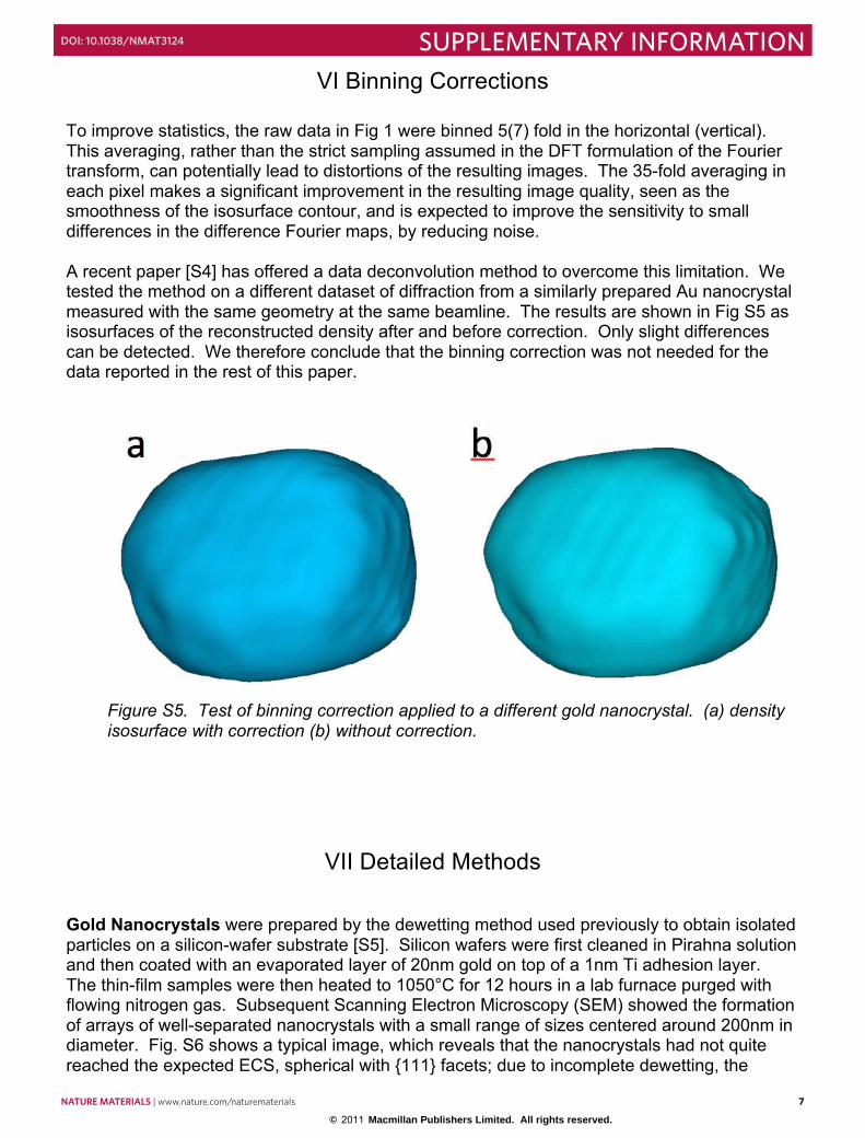
To improve statistics, the raw data in Fig 1 were binned 5(7) fold in the horizontal (vertical). This averaging, rather than the strict sampling assumed in the DFT formulation of the Fourier transform, can potentially lead to distortions of the resulting images. The 35-fold averaging in each pixel makes a significant improvement in the resulting image quality, seen as the smoothness of the isosurface contour, and is expected to improve the sensitivity to small differences in the difference Fourier maps, by reducing noise. A recent paper [S4] has offered a data deconvolution method to overcome this limitation. We tested the method on a different dataset of diffraction from a similarly prepared Au nanocrystal measured with the same geometry at the same beamline. The results are shown in Fig S5 as isosurfaces of the reconstructed density after and before correction. Only slight differences can be detected. We therefore conclude that the binning correction was not needed for the data reported in the rest of this paper.
Figure S5. Test of binning correction applied to a different gold nanocrystal. (a) density isosurface with correction (b) without correction.
VII Detailed Methods Gold Nanocrystals were prepared by the dewetting method used previously to obtain isolated particles on a silicon-wafer substrate [S5]. Silicon wafers were first cleaned in Pirahna solution and then coated with an evaporated layer of 20nm gold on top of a 1nm Ti adhesion layer. The thin-film samples were then heated to 1050°C for 12 hours in a lab furnace purged with flowing nitrogen gas. Subsequent Scanning Electron Microscopy (SEM) showed the formation of arrays of well-separated nanocrystals with a small range of sizes centered around 200nm in diameter. Fig. S6 shows a typical image, which reveals that the nanocrystals had not quite reached the expected ECS, spherical with {111} facets; due to incomplete dewetting, the
NATURE MATERIALS | www.nature.com/naturematerials 7
SUPPLEMENTARY INFORMATIONDOI: 10.1038/NMAT3124
© 2011 Macmillan Publishers Limited. All rights reserved.
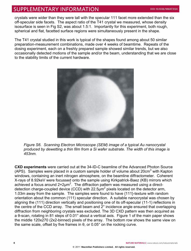
crystals were wider than they were tall with the specular 111 facet more extended than the six off-specular side facets. The aspect ratio of the T41 crystal we measured, whose density isosurface is seen in Fig S2, was about 1.5:1. Importantly for this experiment, both rough, spherical and flat, facetted surface regions were simultaneously present in the shape. The T41 crystal studied in this work is typical of the shapes found among about 50 similar preparation-measurement combinations, made over 4 weeks of beamtime. Repeats of the dosing experiment, each on a freshly prepared sample showed similar trends, but we also occasionally detected motions of the sample and/or the beam, understanding that we are close to the stability limits of the current hardware.
Figure S6. Scanning Electron Microscope (SEM) image of a typical Au nanocrystal produced by dewetting a thin film from a Si wafer substrate. The width of this image is 453nm.
CXD experiments were carried out at the 34-ID-C beamline of the Advanced Photon Source (APS). Samples were placed in a custom sample holder of volume about 20cm3 with Kapton windows, containing an inert nitrogen atmosphere, on the beamline diffractometer. Coherent X-rays of 8.92keV were focussed onto the sample using Kirkpatrick-Baez (KB) mirrors which achieved a focus around 2×2µm2. The diffraction pattern was measured using a direct-detection charge-coupled device (CCD) with 22.5µm2 pixels located on the detector arm, 1.03m away from the sample. The samples were found to have {111}-texture with random orientation about the common (111) specular direction. A suitable nanocrystal was chosen by aligning the (111) direction vertically and positioning one of its off-specular (11-1) reflections in the centre of the CCD array. The small beam and 2° incidence angle ensured that overlapping diffraction from neighboring crystals was excluded. The 3D CXD pattern was then acquired as a θ-scan, rotating in 81 steps of 0.01° about a vertical axis. Figure 1 of the main paper shows the middle 120x270 (2x2-binned) pixels of the array. The bottom row shows the same view on the same scale, offset by five frames in θ, or 0.05° on the rocking curve.
8 NATURE MATERIALS | www.nature.com/naturematerials
SUPPLEMENTARY INFORMATION DOI: 10.1038/NMAT3124
© 2011 Macmillan Publishers Limited. All rights reserved.
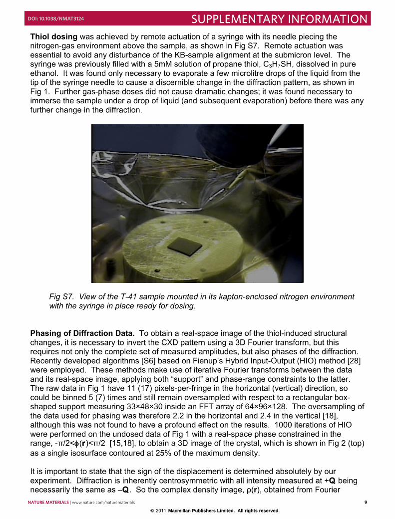
Thiol dosing was achieved by remote actuation of a syringe with its needle piecing the nitrogen-gas environment above the sample, as shown in Fig S7. Remote actuation was essential to avoid any disturbance of the KB-sample alignment at the submicron level. The syringe was previously filled with a 5mM solution of propane thiol, C3H7SH, dissolved in pure ethanol. It was found only necessary to evaporate a few microlitre drops of the liquid from the tip of the syringe needle to cause a discernible change in the diffraction pattern, as shown in Fig 1. Further gas-phase doses did not cause dramatic changes; it was found necessary to immerse the sample under a drop of liquid (and subsequent evaporation) before there was any further change in the diffraction.
Fig S7. View of the T-41 sample mounted in its kapton-enclosed nitrogen environment with the syringe in place ready for dosing.
Phasing of Diffraction Data. To obtain a real-space image of the thiol-induced structural changes, it is necessary to invert the CXD pattern using a 3D Fourier transform, but this requires not only the complete set of measured amplitudes, but also phases of the diffraction. Recently developed algorithms [S6] based on Fienup’s Hybrid Input-Output (HIO) method [28] were employed. These methods make use of iterative Fourier transforms between the data and its real-space image, applying both “support” and phase-range constraints to the latter. The raw data in Fig 1 have 11 (17) pixels-per-fringe in the horizontal (vertical) direction, so could be binned 5 (7) times and still remain oversampled with respect to a rectangular box-shaped support measuring 33×48×30 inside an FFT array of 64×96×128. The oversampling of the data used for phasing was therefore 2.2 in the horizontal and 2.4 in the vertical [18], although this was not found to have a profound effect on the results. 1000 iterations of HIO were performed on the undosed data of Fig 1 with a real-space phase constrained in the range, -π/2<φ(r)<π/2 [15,18], to obtain a 3D image of the crystal, which is shown in Fig 2 (top) as a single isosurface contoured at 25% of the maximum density. It is important to state that the sign of the displacement is determined absolutely by our experiment. Diffraction is inherently centrosymmetric with all intensity measured at +Q being necessarily the same as –Q. So the complex density image, ρ(r), obtained from Fourier
NATURE MATERIALS | www.nature.com/naturematerials 9
SUPPLEMENTARY INFORMATIONDOI: 10.1038/NMAT3124
© 2011 Macmillan Publishers Limited. All rights reserved.
inversion of the measurement is indistinguishable from ρ*(-r). The phasing algorithm used arbitrarily picks one of these two solutions and the shape of the crystal appears as the ‘twin’ about half the time (from different random starting points). We do not know whether the image of the crystal density in Fig 2 is the twin or not. It happens that the crystals made by the dewetting method are fairly symmetric but, based on comparison with SEM, tend to be slightly tapered away from the substrate. We used that observation to assign the ‘top’ and ‘bottom’ (adjacent to the substrate) of the image at the top of Fig 2. However, the parity of the phase function is different since the phase φ(r) is the same for functions ρ(r) and ρ*(-r). It is imperative therefore not to lose track of the directions of the axes, the definition of the direction of Q=k f-ki and the polarity of the Fourier transform throughout all the steps of the data analysis. When Q points away from the sample in the (11-1) direction, the phase of Δρ = ρ(dosed) – ρ(bare) is -π/2 on that side of the crystal, along the negative imaginary axis, so the displacement is inwards: the crystal facet contracts upon dosing with thiol. Finite-element analysis (FEA) using continuum elasticity calculations were used to connect the pattern of strains to the surface stress. The COMSOL FEA package [S7] was used to simulate the strain pattern introduced in a facetted gold sphere of 300nm diameter by a differential surface stress. Four circular flat facets, each subtending 40º, were placed in contact with a thin skin of the same material of thickness h=5nm containing one value of the bulk isotropic stress of σx= σy= σz=σB (in Pa units) over the facets and another value over the spherical surface regions. The surface stress, equal to the “mechanical surface tension”, is then given by σS= σB h in units of N/m or J/m2. This skin serves to model the SAM itself but the strains that form within it are disregarded. The maximum displacement component parallel to the facet seen in Fig 3 is less than the perpendicular value and confined to a tiny corner region. The definition of stress used by the FEA code [S7] agrees with the convention used above. When tensile (positive) stress is applied to the facets, they contract inwards. The FEA calculation shows there is also an inward lateral contraction of the edges of each facet, but this is relatively small compared with the perpendicular strain found to be the largest change seen in the experiment. A large strain is found in the ‘skin’ used to generate the stress, especially near the corners, but this is expected from the artificial cusp introduced in the model of the crystal shape. Cantilever measurements. The experimental setup for these measurements is schematically illustrated in Figure S8. A cantilever array, fabricated from silicon, was coated with 20nm of gold. This was placed into a gas cell with a volume of 300 µl. Reference cantilevers were left uncoated by applying a mask during the gold deposition process. The gas cell was connected to a syringe pump via PTFE (Teflon) tubing and a T-junction. The syringe was pumping nitrogen gas through the system at a constant rate of 0.3 ml/min. A drop of the thiol solution was introduced into the T-junction using a syringe piercing through a rubber cap. Thiol vapour was carried to the gas cell via the nitrogen stream. The resulting cantilever deflection was recorded by optical deflection of a laser beam on a split photodiode [S8].
10 NATURE MATERIALS | www.nature.com/naturematerials
SUPPLEMENTARY INFORMATION DOI: 10.1038/NMAT3124
© 2011 Macmillan Publishers Limited. All rights reserved.
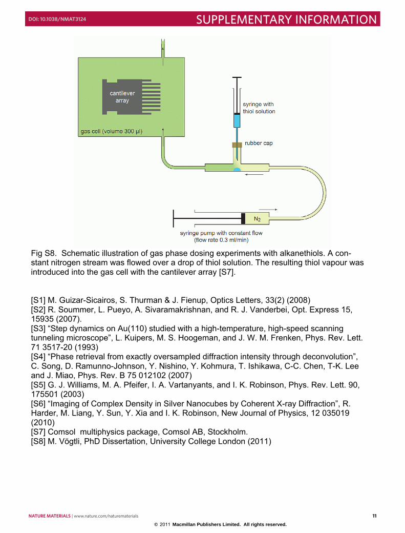
Fig S8. Schematic illustration of gas phase dosing experiments with alkanethiols. A con- stant nitrogen stream was flowed over a drop of thiol solution. The resulting thiol vapour was introduced into the gas cell with the cantilever array [S7]. [S1] M. Guizar-Sicairos, S. Thurman & J. Fienup, Optics Letters, 33(2) (2008) [S2] R. Soummer, L. Pueyo, A. Sivaramakrishnan, and R. J. Vanderbei, Opt. Express 15, 15935 (2007). [S3] “Step dynamics on Au(110) studied with a high-temperature, high-speed scanning tunneling microscope”, L. Kuipers, M. S. Hoogeman, and J. W. M. Frenken, Phys. Rev. Lett. 71 3517-20 (1993) [S4] “Phase retrieval from exactly oversampled diffraction intensity through deconvolution”, C. Song, D. Ramunno-Johnson, Y. Nishino, Y. Kohmura, T. Ishikawa, C-C. Chen, T-K. Lee and J. Miao, Phys. Rev. B 75 012102 (2007) [S5] G. J. Williams, M. A. Pfeifer, I. A. Vartanyants, and I. K. Robinson, Phys. Rev. Lett. 90, 175501 (2003) [S6] “Imaging of Complex Density in Silver Nanocubes by Coherent X-ray Diffraction”, R. Harder, M. Liang, Y. Sun, Y. Xia and I. K. Robinson, New Journal of Physics, 12 035019 (2010) [S7] Comsol multiphysics package, Comsol AB, Stockholm. [S8] M. Vögtli, PhD Dissertation, University College London (2011)
NATURE MATERIALS | www.nature.com/naturematerials 11
SUPPLEMENTARY INFORMATIONDOI: 10.1038/NMAT3124
© 2011 Macmillan Publishers Limited. All rights reserved.