sub 300 nm wavelength iii-nitride tunnel-injected ... 300 nm wavelength iii-nitride tunnel-injected...
TRANSCRIPT

[email protected]; [email protected] Sub 300 nm Wavelength III-Nitride Tunnel-Injected UV LEDs
Sub 300 nm Wavelength III-Nitride Tunnel-Injected Ultraviolet LEDs
Yuewei Zhang, Sriram Krishnamoorthy, Fatih Akyol, Sadia Monika Siddharth Rajan
ECE, The Ohio State University
Andrew Allerman, Michael Moseley, Andrew Armstrong Sandia National Labs
Jared Johnson, Jinwoo Hwang MSE, The Ohio State University
Funding: NSF EECS-1408416

[email protected]; [email protected] Sub 300 nm Wavelength III-Nitride Tunnel-Injected UV LEDs 2
Outline: Tunneling injected UV LED
• Motivation
• Polarization engineered III-Nitride tunnel junctions
• Tunneling junction for hole injection into UV LEDs.
• Electrical characteristics
• Optical characteristics
• Sub-300 nm emission
• Summary

[email protected]; [email protected] Sub 300 nm Wavelength III-Nitride Tunnel-Injected UV LEDs 3
Outline: Tunneling injected UV LED
• Motivation
• Polarization engineered III-Nitride tunnel junctions
• Tunneling junction for hole injection into UV LEDs.
• Electrical characteristics
• Optical characteristics
• Sub-300 nm emission
• Summary

[email protected]; [email protected] Sub 300 nm Wavelength III-Nitride Tunnel-Injected UV LEDs 4
Motivation
UV C UV B UV A 400 nm 315 nm 280 nm 100 nm
UV curing
Printing
Sensing
Phototherapy
Medical imaging
Protein analysis
Drug discovery Sterilization
Sensing
Disinfection
DNA sequencing

[email protected]; [email protected] Sub 300 nm Wavelength III-Nitride Tunnel-Injected UV LEDs 5
Motivation
• UV lighting market is increasing.
• UV LEDs are replacing the traditional UV lamps.
Y. Muramoto, Semicond. Sci. Technol. 29 (2014) 084004.
UV C UV B UV A 400 nm 315 nm 280 nm 100 nm
UV curing
Printing
Sensing
Phototherapy
Medical imaging
Protein analysis
Drug discovery Sterilization
Sensing
Disinfection
DNA sequencing
[email protected]; [email protected] Sub 300 nm Wavelength III-Nitride Tunnel-Injected UV LEDs 6
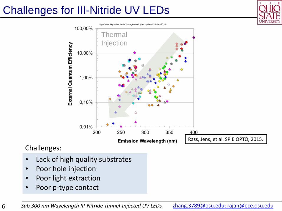
Challenges for III-Nitride UV LEDs
Thermal Injection
Rass, Jens, et al. SPIE OPTO, 2015.
• Lack of high quality substrates • Poor hole injection • Poor light extraction • Poor p-type contact
Challenges:

[email protected]; [email protected] Sub 300 nm Wavelength III-Nitride Tunnel-Injected UV LEDs 7
Challenges for III-Nitride UV LEDs
Thermal Injection
Rass, Jens, et al. SPIE OPTO, 2015.
• Lack of high quality substrates • Poor hole injection • Poor light extraction • Poor p-type contact
Solved by growth optimization Challenges:

[email protected]; [email protected] Sub 300 nm Wavelength III-Nitride Tunnel-Injected UV LEDs 8
Challenges for III-Nitride UV LEDs
• Lack of high quality substrates • Poor hole injection • Poor light extraction • Poor p-type contact
Thermal Injection
Rass, Jens, et al. SPIE OPTO, 2015.
Solved by growth optimization
Caused by high acceptor activation energy in (Al)GaN
Challenges:

[email protected]; [email protected] Sub 300 nm Wavelength III-Nitride Tunnel-Injected UV LEDs 9
Challenges for III-Nitride UV LEDs
• Lack of high quality substrates • Poor hole injection • Poor light extraction • Poor p-type contact
Thermal Injection
Rass, Jens, et al. SPIE OPTO, 2015.
Solved by growth optimization
Caused by high acceptor activation energy in (Al)GaN
Challenges:
Na=1 x 1019 cm-3 GaN: 140 meV, Na-=7 x 1017 cm-3 AlN: 630 meV, Na-=6 x 1013 cm-3

[email protected]; [email protected] Sub 300 nm Wavelength III-Nitride Tunnel-Injected UV LEDs 10
P-contact and light extraction
Trade-off between ƞinjection & ƞLEE
Current designs
p AlGaN
p GaN
MQW
n AlGaN
LED
p AlGaN
p AlGaN/AlGaN SL
MQW
n AlGaN
LED
Absorption loss
Electrical loss
Increased absorption losses
Increased voltage drop

[email protected]; [email protected] Sub 300 nm Wavelength III-Nitride Tunnel-Injected UV LEDs 11
P-contact and light extraction
Current designs Thin p AlGaN
Tunnel Junction
MQW
n AlGaN
n AlGaN
LED
p AlGaN
p GaN
MQW
n AlGaN
LED
p AlGaN
p AlGaN/AlGaN SL
MQW
n AlGaN
LED
Absorption loss
Electrical loss
TJ-UV LED
Tunneling injection

[email protected]; [email protected] Sub 300 nm Wavelength III-Nitride Tunnel-Injected UV LEDs 12
Non-equilibrium injection
Current designs Thin p AlGaN
Tunnel Junction
MQW
n AlGaN
n AlGaN
LED
p AlGaN
p GaN
MQW
n AlGaN
LED
p AlGaN
p AlGaN/AlGaN SL
MQW
n AlGaN
LED
Absorption loss
Electrical loss
TJ-UV LED
VLED e-
h+
e- Ec
Ev
• Replace p-type contact using tunneling contact.
• Non-equilibrium injection.
• Reduced light absorption loss • Better contacts.
Tunneling injection

[email protected]; [email protected] Sub 300 nm Wavelength III-Nitride Tunnel-Injected UV LEDs 13
0 20 40 60 80 100
1E15
1E16
1E17
1E18
Electrons Holes
Carri
er Co
ncen
tratio
n (cm
-3)
Depth (nm)
Electron and hole injection imbalance
Ea=0 meV
Ƞinj = Electrons injected into active region Total electrons
= Holes injected into active regionTotal electrons
~ 𝐽𝐽p
𝐽𝐽n
Va
N- Al0.3Ga0.7N P-Al0.3Ga0.7N
• For ideal junction, equal amount of e/ h are supplied to active region.
• Ƞinj = 1
Jp
Jn

[email protected]; [email protected] Sub 300 nm Wavelength III-Nitride Tunnel-Injected UV LEDs 14
Electron and hole injection imbalance
• For PN junction, hole current is much lower than electron current.
• Low injection efficiency.
Va
N- Al0.3Ga0.7N P-Al0.3Ga0.7N
Ea=0 meV
Real case: 𝐽𝐽n < 𝐽𝐽p ⇒ Ƞinj << 1
Jp
Jn
Electron blocking layer is used to increase Ƞinj
Ƞinj = Electrons injected into active region Total electrons
= Holes injected into active regionTotal electrons
~ 𝐽𝐽p
𝐽𝐽n
0 20 40 60 80 100
1E15
1E16
1E17
1E18
Electrons Holes
Carri
er Co
ncen
tratio
n (cm
-3)
Depth (nm)
Ea=0.22 meV
[email protected]; [email protected] Sub 300 nm Wavelength III-Nitride Tunnel-Injected UV LEDs 15
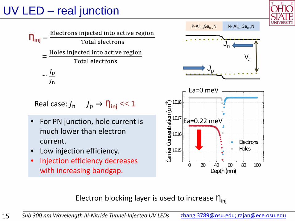
UV LED – real junction
0 20 40 60 80 100
1E15
1E16
1E17
1E18
Electrons Holes
Carri
er Co
ncen
tratio
n (cm
-3)
Depth (nm)
Ea=0.22 meV • For PN junction, hole current is much lower than electron current.
• Low injection efficiency. • Injection efficiency decreases
with increasing bandgap.
Va
N- Al0.3Ga0.7N P-Al0.3Ga0.7N
Ea=0 meV
Real case: 𝐽𝐽n < 𝐽𝐽p ⇒ Ƞinj << 1
Jp
Jn
Electron blocking layer is used to increase Ƞinj
Ƞinj = Electrons injected into active region Total electrons
= Holes injected into active regionTotal electrons
~ 𝐽𝐽p
𝐽𝐽n

[email protected]; [email protected] Sub 300 nm Wavelength III-Nitride Tunnel-Injected UV LEDs 16
Tunneling injection into UV LEDs
Ƞinj ~ 𝐽𝐽p
𝐽𝐽n ~ 𝐽𝐽tunnel
𝐽𝐽n
Jp = Jtunnel
Jn
Va
Thin p AlGaN
Tunnel Junction
MQW
n AlGaN
n AlGaN
LED
TJ-UV LED
e-
h+
e-
• Tunneling injection enables high hole current.
• Increased injection efficiency. • Injection efficiency not sensitive
to the increasing bandgap.

[email protected]; [email protected] Sub 300 nm Wavelength III-Nitride Tunnel-Injected UV LEDs 17
Tunneling injection into UV LEDs
• Tunneling injection enables high hole current.
• Increased injection efficiency. • Injection efficiency not sensitive
to the increasing bandgap.
Ƞinj ~ 𝐽𝐽p
𝐽𝐽n ~ 𝐽𝐽tunnel
𝐽𝐽n
Jp = Jtunnel
Jn
Va
Thin p AlGaN
Tunnel Junction
MQW
n AlGaN
n AlGaN
LED
TJ-UV LED
e-
h+
e-
Required TJ characteristics Voltage drop across TJ should be low On-resistance should be minimal Optical absorption should be minimal
[email protected]; [email protected] Sub 300 nm Wavelength III-Nitride Tunnel-Injected UV LEDs 18
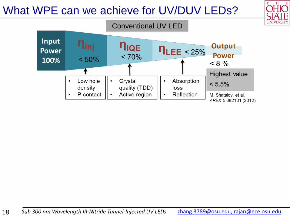
What WPE can we achieve for UV/DUV LEDs? Conventional UV LED

[email protected]; [email protected] Sub 300 nm Wavelength III-Nitride Tunnel-Injected UV LEDs 19
What WPE can we achieve for UV/DUV LEDs? Conventional UV LED
Tunneling injected UV LED
[email protected]; [email protected] Sub 300 nm Wavelength III-Nitride Tunnel-Injected UV LEDs 20
Outline: Tunneling injected UV LED
• Motivation
• Polarization engineered III-Nitride tunnel junctions
• Tunneling junction for hole injection into UV LEDs.
• Electrical characteristics
• Optical characteristics
• Sub-300 nm emission
• Summary

[email protected]; [email protected] Sub 300 nm Wavelength III-Nitride Tunnel-Injected UV LEDs 21
Polarization engineering for tunnel junctions
Standard p+/n+ TJ
• Large Eg wide depletion region • Doping limitations • Large energy barrier for tunneling
Low tunneling current density

[email protected]; [email protected] Sub 300 nm Wavelength III-Nitride Tunnel-Injected UV LEDs 22
Polarization engineering for tunnel junctions
n+ (Al)GaN p+ (Al)GaN
+σ
-σ
InG
aN
Standard p+/n+ TJ
• Large Eg wide depletion region • Doping limitations • Large energy barrier for tunneling
Low tunneling current density
Polarization TJ
• High density polarization sheet charge
depletion width greatly reduced. • Tunnel barrier reduced due to InGaN.
AlN barrier TJ: Previous Work M. J. Grundmann, PhD Dissertation (UCSB) J. Simon et.al., PRL 103, 026801 (2009) (Notre Dame)

[email protected]; [email protected] Sub 300 nm Wavelength III-Nitride Tunnel-Injected UV LEDs 23
Overview of the tunnel junction technology
1 2 3 4 510-8
10-6
10-4
10-2
100
102
GaAs
GaSb
/InAs
InP
GaN
AlGa
As/In
AlGa
P
TJ
resis
tance
(Ω cm
2 )
Bandgap (eV)
GaN/AlN GaN/AlN
GdN/GaN
InGaN/GaN
Nano Lett., 13, 2570 (2013)
APL 102, 113503 (2013)
Resistance down to 10-4 Ohm cm2 achieved for GaN tunnel junctions.

[email protected]; [email protected] Sub 300 nm Wavelength III-Nitride Tunnel-Injected UV LEDs 24
Overview of the tunnel junction technology
1 2 3 4 510-8
10-6
10-4
10-2
100
102
GaAs
GaSb
/InAs
InP
GaN
AlGa
As/In
AlGa
P
TJ
resis
tance
(Ω cm
2 )
Bandgap (eV)
GaN/AlN GaN/AlN
?
GdN/GaN
InGaN/GaN
Resistance down to 10-4 Ohm cm2 achieved for GaN tunnel junctions.
What would happen when we go to wider bandgap (AlGaN)?
Nano Lett., 13, 2570 (2013)
APL 102, 113503 (2013)

[email protected]; [email protected] Sub 300 nm Wavelength III-Nitride Tunnel-Injected UV LEDs 25
Modeling: tunneling current
• Self-consistent Schrodinger Poisson solution • WKB approximation for tunneling probability
calculation.
( )n p n nT p n z wkbJ q f f v T dEρ ρ= −∫∫
N- Al0.55Ga0.45N P-Al0.55Ga0.45N
In0.
2Ga 0.
8N
-4
-2
0
2
4
Ener
gy (e
V)
Depth (nm)
φn
φp

[email protected]; [email protected] Sub 300 nm Wavelength III-Nitride Tunnel-Injected UV LEDs 26
-4
-2
0
2
4
Ener
gy (e
V)
Depth (nm)
φn
φp
Modeling: tunneling current
1 10 100 10001E-4
1E-3
0.01
Resis
tanc
e (Oh
m cm
2 )
Current Density (A/cm2)
0 1 2 30
1k
2k
Curre
nt D
ensit
y (A/
cm2 )
Voltage (V)
• Resistance reaches 7E-4 Ohm cm2. • High current density could be achieved
with low voltage drop.
N- Al0.55Ga0.45N P-Al0.55Ga0.45N
In0.
2Ga 0.
8N
• Self-consistent Schrodinger Poisson solution • WKB approximation for tunneling probability
calculation.
( )n p n nT p n z wkbJ q f f v T dEρ ρ= −∫∫

[email protected]; [email protected] Sub 300 nm Wavelength III-Nitride Tunnel-Injected UV LEDs 27
0.2 0.4 0.6 0.8
10-6
10-5
10-4
10-3
TJ
Res
istan
ce (Ω
cm
2 )
InGaN composition
MODEL
Beyond the GaN bandgap: Design of AlGaN TJs
• Low resistance TJ could be created for high composition AlGaN.
• Hole injection could be achieved through high bandgap AlGaN TJs.
1 2 3 4 510-8
10-6
10-4
10-2
100
102
GaAs
GaSb
/InAs
InP
GaN
AlGa
As/In
AlGa
P
TJ
resis
tance
(Ω cm
2 )
Bandgap (eV)
GaN/AlN GaN/AlN
GdN/GaN
InGaN/GaN
70%
50%
30%
20%
10%
AlxGa1-xN ?

[email protected]; [email protected] Sub 300 nm Wavelength III-Nitride Tunnel-Injected UV LEDs 28
Outline: Tunneling injected UV LED
• Motivation
• Polarization engineered III-Nitride tunnel junctions
• Tunneling junction for hole injection into UV LEDs.
• Electrical characteristics
• Optical characteristics
• Sub-300 nm emission
• Summary

[email protected]; [email protected] Sub 300 nm Wavelength III-Nitride Tunnel-Injected UV LEDs 29
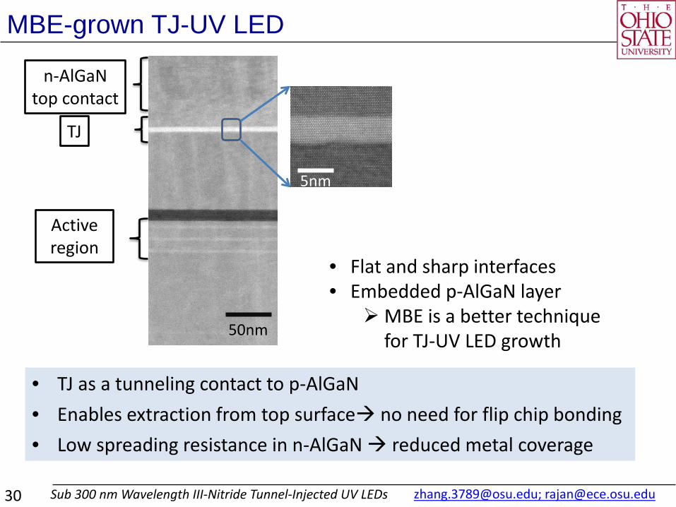
MBE-grown TJ-UV LED
TJ
n-AlGaN top contact
Active region
• TJ as a tunneling contact to p-AlGaN • Enables extraction from top surface no need for flip chip bonding • Low spreading resistance in n-AlGaN reduced metal coverage
+c
QWs
TJ
-4 -2 0 2 4
150
100
50
0
Dept
h (nm
)
Energy (eV)N-Al0.3Ga0.7N on
Sapphire
50 nm n-Al0.3Ga0.7N [Si] =3 X 1018 cm-3
4 nm In0.25Ga0.75N
50 nm p-Al0.3Ga0.7N [Mg] = 2X 1019 cm-3
100 nm n-Al0.3Ga0.7N [Si] = 5 X 1019 cm-3
300 nm n-Al0.3Ga0.7N [Si] =1.2 X 1019 cm-3
12 nm p type Al0.46Ga0.54N
15 nm p+ -Al0.3Ga0.7N [Mg] = 5 X 1019 cm-3
15 nm n+ AlGaN [Si] = 1 X 1020 cm-3
QWs
50nm
[email protected]; [email protected] Sub 300 nm Wavelength III-Nitride Tunnel-Injected UV LEDs 30
MBE-grown TJ-UV LED
TJ
n-AlGaN top contact
• TJ as a tunneling contact to p-AlGaN • Enables extraction from top surface no need for flip chip bonding • Low spreading resistance in n-AlGaN reduced metal coverage
50nm
5nm
• Flat and sharp interfaces • Embedded p-AlGaN layer MBE is a better technique
for TJ-UV LED growth
Active region

[email protected]; [email protected] Sub 300 nm Wavelength III-Nitride Tunnel-Injected UV LEDs 31
TJ-UV LED – optical characteristics
280 300 320 340 360 380 400 4200
1x10⁴
2x10⁴
3x10⁴
4x10⁴
5x10⁴In
tens
ity (a
.u.)
Wavelength (nm)
RT, CW 0.1mA to 20mA
50µm device
0 5 10 15 200.0
0.1
0.2
0.3
0.4
0.5
0.6
Powe
r (m
W)
Current (mA)
0 5 10 15 200.2
0.4
0.6
0.8
1.0
1.2
1.4
1.6W
PE (%
)
EQE (
%)
Current (mA)0.2
0.4
0.6
0.8
1.0
1.2
1.4 • Single peak emission at 327 nm • Peak EQE and WPE are 1.5% and
1.08%, respectively. • At 120 A/cm2, voltage is 5.9 V,
power is 6 W/cm2. • Proof of efficient hole injection
through tunneling.
Y. Zhang, Appl. Phys. Lett. 106, 141103 (2015)
On-wafer measurement

[email protected]; [email protected] Sub 300 nm Wavelength III-Nitride Tunnel-Injected UV LEDs 32
TJ-UV LED – electrical characteristics
-6 -4 -2 0 2 4 60
1k
2k Full metal coverage L shape metal
Curre
nt D
ensit
y (A/
cm2 )
Voltage (V)
-6 -4 -2 0 2 4 61n100n10µ1m
100m101k
Curre
nt D
ensit
y (A/
cm2 )
Voltage (V)1 10 100 100010-4
10-3
10-2
10-1
100
Experiment Simulation
Resis
tanc
e (Ω
cm2 )
Current Density (A/cm2)
• Lowest TJ resistance of 5.6 x 10⁻⁴ Ohm cm2 is obtained for Al0.3Ga0.7N TJ
Forward Resistance = Rseries + RTJ + Rc
Voltage @ J=20 A/cm2
Voltage @ J=2 kA/cm2
R @ 2 kA/cm2
(50um*50um)
4.8 V 7.47 V 7.5E-04 Ohm cm2
1.9E-04 ~ 1E-06 Ohm cm2

[email protected]; [email protected] Sub 300 nm Wavelength III-Nitride Tunnel-Injected UV LEDs 33
TJ-UV LED – electrical characteristics
-6 -4 -2 0 2 4 60
1k
2k Full metal coverage L shape metal
Curre
nt D
ensit
y (A/
cm2 )
Voltage (V)
-6 -4 -2 0 2 4 61n100n10µ1m
100m101k
Curre
nt D
ensit
y (A/
cm2 )
Voltage (V)1 10 100 100010-4
10-3
10-2
10-1
100
Experiment Simulation
Resis
tanc
e (Ω
cm2 )
Current Density (A/cm2)
• Lowest TJ resistance of 5.6 x 10⁻⁴ Ohm cm2 is obtained for Al0.3Ga0.7N TJ
• Polarization engineered TJ enables orders of magnitude lower resistance.

[email protected]; [email protected] Sub 300 nm Wavelength III-Nitride Tunnel-Injected UV LEDs 34
TJ-UV LED – Sub-300 nm emission
+c
QWs
TJ
Al0.78Ga0.22N on Sapphire
50 nm n-Al0.55Ga0.45N [Si] =3 X 1018 cm-3
4 nm In0.2Ga0.8N
20 nm p-Al0.55Ga0.45N [Mg] = 2X 1019 cm-3
300 nm n-Al0.55Ga0.45N [Si] = 5 X 1019 cm-3
600 nm graded to n-Al0.55Ga0.45N
[Si] =1.2 X 1019 cm-3
8 nm p type Al0.72Ga0.28N
15 nm p+ -AlGaN [Mg] = 5 X 1019 cm-3
15 nm n+ AlGaN [Si] = 1 X 1020 cm-3
QWs
030
6090
120
-4 -2 0 2 4
Energy (eV) Depth (nm
)
-6 -4 -2 0 2 4 6 8 10 120
200
400
600
800
1000
1200
Curre
nt D
ensit
y (A/
cm2 )
Voltage (V)
-6 -4 -2 0 2 4 6 8 10 121E-3
0.01
0.1
1
10
100
1000
Curre
nt D
ensit
y (A
/cm
2 )
Voltage (V)
1 10 100 10001E-4
1E-3
0.01
0.1
1
Resis
tanc
e (Oh
m cm
2 )
Current Density (A/cm2)
• Voltage @ 20A/cm2 is 7.1 V. • Resistance @ 1kA/cm2 is
1.6E-3 Ohm cm2

[email protected]; [email protected] Sub 300 nm Wavelength III-Nitride Tunnel-Injected UV LEDs 35
TJ-UV LED – Sub-300 nm emission
+c
QWs
TJ
Al0.78Ga0.22N on Sapphire
50 nm n-Al0.55Ga0.45N [Si] =3 X 1018 cm-3
4 nm In0.2Ga0.8N
20 nm p-Al0.55Ga0.45N [Mg] = 2X 1019 cm-3
300 nm n-Al0.55Ga0.45N [Si] = 5 X 1019 cm-3
600 nm graded to n-Al0.55Ga0.45N
[Si] =1.2 X 1019 cm-3
8 nm p type Al0.72Ga0.28N
15 nm p+ -AlGaN [Mg] = 5 X 1019 cm-3
15 nm n+ AlGaN [Si] = 1 X 1020 cm-3
QWs
030
6090
120
-4 -2 0 2 4
Energy (eV) Depth (nm
)
-6 -4 -2 0 2 4 6 8 10 120
200
400
600
800
1000
1200
Curre
nt D
ensit
y (A/
cm2 )
Voltage (V)
-6 -4 -2 0 2 4 6 8 10 121E-3
0.01
0.1
1
10
100
1000
Curre
nt D
ensit
y (A
/cm
2 )
Voltage (V)
• Voltage @ 20A/cm2 is 7.1 V. • Resistance @ 1kA/cm2 is
1.6E-3 Ohm cm2 1 2 3 4 510-8
10-6
10-4
10-2
100
102
Al0.
55Ga
0.45
N
Al0.
3Ga 0.
7N
GaAs
GaSb
/InAs
InP
GaN
AlGa
As/In
AlGa
P
TJ re
sistan
ce (Ω
cm2 )
Bandgap (eV)
This work
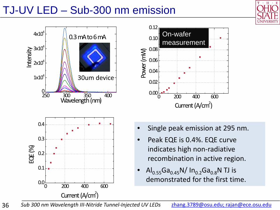
[email protected]; [email protected] Sub 300 nm Wavelength III-Nitride Tunnel-Injected UV LEDs 36
0 200 400 6000.0
0.1
0.2
0.3
0.4
EQE (
%)
Current (A/cm2)
0 200 400 6000.00
0.02
0.04
0.06
0.08
0.10
0.12
Powe
r (m
W)
Current (A/cm2)
TJ-UV LED – Sub-300 nm emission
• Single peak emission at 295 nm. • Peak EQE is 0.4%. EQE curve
indicates high non-radiative recombination in active region.
• Al0.55Ga0.45N/ In0.2Ga0.8N TJ is demonstrated for the first time.
250 300 350 4000
1x10⁴
2x10⁴
3x10⁴
4x10⁴In
tens
ity
Wavelength (nm)
0.3 mA to 6 mA
30um device
On-wafer measurement

[email protected]; [email protected] Sub 300 nm Wavelength III-Nitride Tunnel-Injected UV LEDs 37
Outline: Tunneling injected UV LED
• Motivation
• Polarization engineered III-Nitride tunnel junctions
• Tunneling junction for hole injection into UV LEDs.
• Electrical characteristics
• Optical characteristics
• Sub-300 nm emission
• Summary

[email protected]; [email protected] Sub 300 nm Wavelength III-Nitride Tunnel-Injected UV LEDs 38
Summary
First report of tunneling hole injection through wide band gap Al0.55Ga0.45N
tunnel Junctions with Eg ~ 4.7 eV.
• Single peak emission at 295 nm
• Tunneling injection gives EQE of 0.4% (on-wafer)
• Lowest TJ resistance of 1.6E-3 Ohm cm2
Tunnel Junctions are promising for high efficiency UV/ DUV LEDs
1 2 3 4 510-8
10-6
10-4
10-2
100
102
Al0.
55Ga
0.45
N
Al0.
3Ga 0.
7N
GaAs
GaSb
/InAs
InP
GaN
AlGa
As/In
AlGa
P
TJ re
sistan
ce (Ω
cm2 )
Bandgap (eV)
This work
250 300 350 4000.0
5.0x1031.0x1041.5x1042.0x1042.5x1043.0x1043.5x1044.0x1044.5x104
Inte
nsity
Wavelength (nm)
0.3 mA to 6 mA
30um device
-6 -4 -2 0 2 4 6 8 10 120
200
400
600
800
1000
1200
Curre
nt D
ensit
y (A/
cm2 )
Voltage (V)
-6 -4 -2 0 2 4 6 8 10 121E-3
0.01
0.1
1
10
100
1000
Curre
nt D
ensit
y (A
/cm
2 )
Voltage (V)

[email protected]; [email protected] Sub 300 nm Wavelength III-Nitride Tunnel-Injected UV LEDs
UV Tunnel Junction LEDs
Backup slides

[email protected]; [email protected] Sub 300 nm Wavelength III-Nitride Tunnel-Injected UV LEDs 40 40
Absorption losses due to TJ
n AlGaN
p AlGaN
Hole injected back into the active region “recycled” Absorbed/injected back/ emitted recursively
𝐼𝐼𝐼𝐼=𝐼𝐼0exp (−𝛼𝛼t)
1−Loss= T + T(1-T)R + T(1-T)2R2+ T(1-T)3R3 + … + T(1-T)NRN
Absorption loss = 2% ,assuming IQE – 50%
• absorption coefficient (α) of 1×105 cm-1 • 3.9% photons absorbed in one pass • 0.039*IQE is emitted again, and absorbed

[email protected]; [email protected] Sub 300 nm Wavelength III-Nitride Tunnel-Injected UV LEDs 41
Tunable wavelength
41
260 280 300 320 340 360 380 400 420
Inte
nsity
Wavelength (nm)
20% AlGaN QW
10% AlGaN QW
0 2 4 6 8 1012.012.513.013.514.014.515.015.516.0
10% AlGaN QW 20% AlGaN QW
FWHM
Current (mA)

[email protected]; [email protected] Sub 300 nm Wavelength III-Nitride Tunnel-Injected UV LEDs 42
Output power with time
42
-1 0 1 2 3 4 5 6 7 8 945
46
47
48
49
50
51
52
Powe
r (uW
atts)
Time (hr)0 1 2 3 4 5 6 7 8
96
97
98
99
100
101
102
103
Powe
r (uW
atts)
Time (hr)
1 mA 40A/cm2
2 mA 80A/cm2
• Power increases by about 6% and 4% with time for 1mA and 2mA, respectively. Power decreases by 4% for 4mA.
0 1 2 3 4 5 6 7 8 9141142143144145146147148149150151
Powe
r (uW
atts)
Time (hr)
4 mA 160A/cm2

[email protected]; [email protected] Sub 300 nm Wavelength III-Nitride Tunnel-Injected UV LEDs 43
What WPE can we achieve for UV/DUV LEDs?
Input Power 100%
Output Power
ƞinj ƞIQE
Non-equilibrium injection
• Crystal quality (TDD)
• Active region
Minimal absorption (similar to visible LEDs)
< 80% < 70% ~ 45%
ƞLEE < 80% Thin p AlGaN
Tunnel Junction
MQW n AlGaN
n AlGaN
LED
TJ-UV LED
p AlGaN
p GaN
MQW
n AlGaN
LED
p AlGaN
p AlGaN/AlGaN SL
MQW
n AlGaN
LED
Absorption loss
Electrical loss
Input Power 100%
Output Power
ƞinj ƞIQE ƞLEE
• Low hole density
• P-contact
• Crystal quality (TDD)
• Active region
• Absorption loss
• Reflection
< 50% < 70% < 25%
< 8 %
M. Shatalov, et al. APEX 5 082101 (201
Highest value < 5.5%

[email protected]; [email protected] Sub 300 nm Wavelength III-Nitride Tunnel-Injected UV LEDs 44 44
• First report of Al0.3Ga0.7 N interband Tunnel Junctions (TJ) for hole injection in UV LEDs
• Low TJ resistance of 5.6 x 10⁻⁴ ohm cm2
• 327 nm LEDs with 0.58 mW at 20 mA (on-wafer)
• Peak EQE – 1.5%, Peak WPE – 1.08%
• Stable output power of 6 W/cm2 @ 120 A/cm2 @ 5.9 V
Key Results

[email protected]; [email protected] Sub 300 nm Wavelength III-Nitride Tunnel-Injected UV LEDs 45 45
Backup slides
• Absorption losses.. • Calculation details… • Exact quantum well design.. • Tunable wavelength.. • Stability/ reliability of output power! • All previous tunnel junction work! • Latest MOCVD Work!