study and realization of a data conversion chain for very
TRANSCRIPT

HAL Id: tel-03155662https://tel.archives-ouvertes.fr/tel-03155662
Submitted on 2 Mar 2021
HAL is a multi-disciplinary open accessarchive for the deposit and dissemination of sci-entific research documents, whether they are pub-lished or not. The documents may come fromteaching and research institutions in France orabroad, or from public or private research centers.
L’archive ouverte pluridisciplinaire HAL, estdestinée au dépôt et à la diffusion de documentsscientifiques de niveau recherche, publiés ou non,émanant des établissements d’enseignement et derecherche français ou étrangers, des laboratoirespublics ou privés.
Study and realization of a data conversion chain for veryhigh speed digital links
David Cordova
To cite this version:David Cordova. Study and realization of a data conversion chain for very high speed digital links.Electronics. Université de Bordeaux, 2020. English. NNT : 2020BORD0269. tel-03155662

THÈSE PRÉSENTÉE
POUR OBTENIR LE GRADE DE
DOCTEUR DEL’UNIVERSITÉ DE BORDEAUX
École Doctorale des Sciences de l’Ingénieur
Spécialité : Électronique
Présentée et soutenue par
David CORDOVA
Étude et réalisation d’une chaîne de
conversion de données pour liaisons
numériques à très haut débit
Thèse dirigée par Yann DEVAL
Préparée à MACOM Sophia Antipolis
et au Laboratoire IMS
soutenue le: 9 Décembre 2020
Devant la commission d’examen formée de :
Didier BELOT Ingénieur HDR CEA-LETI RapporteurPatricia DESGREYS Professeur Telecom Paris RapporteurJean-Baptiste BEGUERET Professeur Université de Bordeaux ExaminateurWim COPS Ingénieur MACOM InvitéYann DEVAL Professeur Bordeaux INP DirecteurHervé LAPUYADE Maitre de Conférences Université de Bordeaux Co-encadrantYohan PICCIN Ingénieur MACOM ExaminateurNicolas NODENOT Ingénieur MACOM ExaminateurFrançois RIVET Maitre de Conférences HDR Bordeaux INP Co-encadrant

Thèse réalisée au Laboratoire de l’Intégration du Matériau au Système (IMS)
de Bordeaux, au sein de l’équipe CAS du groupe Conception.
Laboratoire IMS – Bâtiment A31
351 Cours de la Libération
33405 Talence Cedex
Thèse CIFRE réalisée dans l’entreprise MACOM,
au sein de l’équipe High-Performance-Analog Design.
MACOM TECHNOLOGIES SOLUTIONS SAS
DRAKKAR Bâtiment C – 1er ETAGE
2405 Route Des Dolines – BP 161
06903 Sophia Antipolis Cedex

Étude et réalisation d’une chaîne de conversion de donnéespour liaisons numériques à très haut debit.
Résumé: La demande croissante de débits de données plus élevés dans les centres
de données a conduit à de nouveaux protocoles émergents (100 - 400G Ethernet et
autres) dans les communications filaires. Ces protocoles favoriseront des encodages
plus sophistiqués utilisant moins de bande passante de fréquence. Les exigences
de vitesse devenant plus strictes, les architectures analogiques pures ne peuvent y
répondre. Ainsi, un virage naturel vers des architectures à signaux mixtes est attendu.
Cette thèse propose la conception d’une architecture de récepteur basée sur un
Convertisseur Analogique-Numérique (CAN). Il utilise une méthodologie de conception
pour définir et valider les exigences et les spécifications des récepteurs filaires à base de
silicium qui sont conformes à un fonctionnement supérieur à >100Gb/s sur des canaux
de transmission avec des pertes élevées (>20dB). Un prototype en technologie 22nm
CMOS FDSOI est proposé comme preuve de concept.
Mot clés: Centre de données, 100 Gigabit Ethernet, PAM4, Convertisseur
Analogique-Numérique, Récepteur, Égalisation

Study and Realization of a Data Conversion Chain for VeryHigh Speed Digital Links.
Abstract: The increasing demand of higher data rates in datacenters has led to new
emerging standards (100 - 400G Ethernet and others) in wireline communications.
These standards will favor more sophisticated encodings that use less frequency
bandwidth. As speed requirements become more stringent, pure analog architectures
can not meet them. So, a natural shift towards mixed-signal architectures is expected.
This thesis proposes the design of an ADC-based receiver architecture. It uses
a design methodology to define and validate the requirements and specifications
for silicon-based wireline receivers that comply with >100Gb/s operation over
transmission channels with high losses (>20dB). A prototype in 22nm CMOS FDSOI
technology is proposed as proof of concept.
Keywords: Datacenters, 100 Gigabit Ethernet, PAM4, Analog-to-Digital Converter,
Receiver, Equalization

Acknowledgments
I have been fortunate to interact with so many wonderful people during the course of
my Ph.D. I want to take this opportunity to thank those who played a big role in the
completion of this work.
First of all, I would like to thank the members of the defense committee for the
interest they took in this work. Thank you Dr. Didier Belor and Professor Patricia
Desgreys for being on my reading committee and for providing me with valuable
comments and also Professor Jean-Baptiste Begueret for chairing my defense.
I would like to express my sincerest thanks and deepest gratitude to my thesis
supervisors. Thanks Yann and And Hervé, for providing me with the opportunity to
study in France and providing expert guidance along the way. François, thank you for
being a humorous and optimistic figure who constantly provides the positive energy
any student needs during the up and downs of a Ph.D.
Special thanks to my industry mentors from MACOM: Wim Cops, Nicolas Nodenot
and Yohan Piccin. I am thankful for the sheer amount of wisdom and learning
experience they have shared with me. Their guidance have greatly improved the
quality of this thesis.
Thank you to all my colleagues at the IMS laboratory and at MACOM for
contributing to the excellent working atmosphere. I especially thank the members
of the CAS team, past and present.
I also need to express my gratitude towards my family for the support they provided
me through my entire life without whose love, encouragement, I would not have finished
this dissertation.
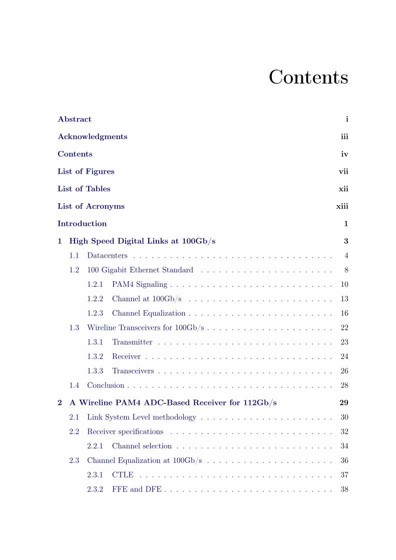
Contents
Abstract i
Acknowledgments iii
Contents iv
List of Figures vii
List of Tables xii
List of Acronyms xiii
Introduction 1
1 High Speed Digital Links at 100Gb/s 3
1.1 Datacenters . . . . . . . . . . . . . . . . . . . . . . . . . . . . . . . . . 4
1.2 100 Gigabit Ethernet Standard . . . . . . . . . . . . . . . . . . . . . . 8
1.2.1 PAM4 Signaling . . . . . . . . . . . . . . . . . . . . . . . . . . . 10
1.2.2 Channel at 100Gb/s . . . . . . . . . . . . . . . . . . . . . . . . 13
1.2.3 Channel Equalization . . . . . . . . . . . . . . . . . . . . . . . . 16
1.3 Wireline Transceivers for 100Gb/s . . . . . . . . . . . . . . . . . . . . . 22
1.3.1 Transmitter . . . . . . . . . . . . . . . . . . . . . . . . . . . . . 23
1.3.2 Receiver . . . . . . . . . . . . . . . . . . . . . . . . . . . . . . . 24
1.3.3 Transceivers . . . . . . . . . . . . . . . . . . . . . . . . . . . . . 26
1.4 Conclusion . . . . . . . . . . . . . . . . . . . . . . . . . . . . . . . . . . 28
2 A Wireline PAM4 ADC-Based Receiver for 112Gb/s 29
2.1 Link System Level methodology . . . . . . . . . . . . . . . . . . . . . . 30
2.2 Receiver specifications . . . . . . . . . . . . . . . . . . . . . . . . . . . 32
2.2.1 Channel selection . . . . . . . . . . . . . . . . . . . . . . . . . . 34
2.3 Channel Equalization at 100Gb/s . . . . . . . . . . . . . . . . . . . . . 36
2.3.1 CTLE . . . . . . . . . . . . . . . . . . . . . . . . . . . . . . . . 37
2.3.2 FFE and DFE . . . . . . . . . . . . . . . . . . . . . . . . . . . . 38

Contents v
2.4 Link System Simulation . . . . . . . . . . . . . . . . . . . . . . . . . . 40
2.4.1 Link Description . . . . . . . . . . . . . . . . . . . . . . . . . . 40
2.4.2 PAM4 BER calculation based on PDF estimation . . . . . . . . 42
2.4.3 Simulation results . . . . . . . . . . . . . . . . . . . . . . . . . . 45
2.5 Conclusion . . . . . . . . . . . . . . . . . . . . . . . . . . . . . . . . . . 50
3 7b 56GS/s Hierarchical Time-Interleaved SAR ADC 51
3.1 Design Flow . . . . . . . . . . . . . . . . . . . . . . . . . . . . . . . . . 52
3.2 Time-Interleaved ADCs . . . . . . . . . . . . . . . . . . . . . . . . . . . 52
3.2.1 Fundamentals of Time-Interleaved ADCs . . . . . . . . . . . . . 52
3.2.2 Signal-to-Noise . . . . . . . . . . . . . . . . . . . . . . . . . . . 57
3.2.3 ADC resolution estimation . . . . . . . . . . . . . . . . . . . . . 58
3.3 Hierarchical TI-ADC . . . . . . . . . . . . . . . . . . . . . . . . . . . . 60
3.3.1 Sampling capacitor estimation . . . . . . . . . . . . . . . . . . . 60
3.3.2 Direct and Inline Demux Sampling . . . . . . . . . . . . . . . . 61
3.3.3 3-Rank Hierarchical TI-ADC . . . . . . . . . . . . . . . . . . . . 65
3.4 Clock generation and distribution . . . . . . . . . . . . . . . . . . . . . 74
3.5 Sub-ADC implementation . . . . . . . . . . . . . . . . . . . . . . . . . 78
3.5.1 Architecture Selection . . . . . . . . . . . . . . . . . . . . . . . 78
3.5.2 Circuit Description . . . . . . . . . . . . . . . . . . . . . . . . . 80
3.5.3 Capacitive DAC . . . . . . . . . . . . . . . . . . . . . . . . . . . 82
3.5.4 Comparator . . . . . . . . . . . . . . . . . . . . . . . . . . . . . 84
3.5.5 SAR Logic . . . . . . . . . . . . . . . . . . . . . . . . . . . . . . 86
3.6 Simulation Results . . . . . . . . . . . . . . . . . . . . . . . . . . . . . 87
3.6.1 Sub-ADC . . . . . . . . . . . . . . . . . . . . . . . . . . . . . . 87
3.6.2 TI-ADC . . . . . . . . . . . . . . . . . . . . . . . . . . . . . . . 92
3.7 Conclusion . . . . . . . . . . . . . . . . . . . . . . . . . . . . . . . . . . 97
4 ADC-RX prototype and prospects 98
4.1 ADC-RX prototype . . . . . . . . . . . . . . . . . . . . . . . . . . . . . 99
4.1.1 Top-level diagram . . . . . . . . . . . . . . . . . . . . . . . . . . 99
vi Contents
4.1.2 Chip layout . . . . . . . . . . . . . . . . . . . . . . . . . . . . . 108
4.2 Prospects . . . . . . . . . . . . . . . . . . . . . . . . . . . . . . . . . . 114
4.2.1 Chip Tapeout . . . . . . . . . . . . . . . . . . . . . . . . . . . . 114
4.2.2 Speed augmentation and improvements . . . . . . . . . . . . . . 115
4.3 Conclusion . . . . . . . . . . . . . . . . . . . . . . . . . . . . . . . . . . 119
Conclusion 120
Publications 122
Appendices 123
A PDK Extraction and Characterization 124
A.1 PDK Extraction . . . . . . . . . . . . . . . . . . . . . . . . . . . . . . . 124
A.2 Switch design . . . . . . . . . . . . . . . . . . . . . . . . . . . . . . . . 127
B Back Gate Biasing Calibration Methodology 130
B.1 Comparator Test Bench . . . . . . . . . . . . . . . . . . . . . . . . . . 130
B.1.1 Offset Extraction . . . . . . . . . . . . . . . . . . . . . . . . . . 131
B.1.2 Comparator . . . . . . . . . . . . . . . . . . . . . . . . . . . . . 132
B.1.3 Back gate biasing DAC . . . . . . . . . . . . . . . . . . . . . . . 133
B.1.4 Offset Calibration . . . . . . . . . . . . . . . . . . . . . . . . . . 135
B.2 Simulation Results . . . . . . . . . . . . . . . . . . . . . . . . . . . . . 135
Bibliography 138

List of Figures
1.1 TierPoint datacenters. . . . . . . . . . . . . . . . . . . . . . . . . . . . 4
1.2 Global IP Traffic Growth [1] . . . . . . . . . . . . . . . . . . . . . . . . 5
1.3 Ethernet Applications. . . . . . . . . . . . . . . . . . . . . . . . . . . . 6
1.4 Ethernet Roadmap: Path to 100GbE single lane. . . . . . . . . . . . . . 7
1.5 Simple link model. . . . . . . . . . . . . . . . . . . . . . . . . . . . . . 8
1.6 OIF’s Common Electrical I/O (CEI) 112G reach projects. . . . . . . . 9
1.7 Data rate vs Parallelization for different modulation schemes. . . . . . . 9
1.8 NRZ and PAM4 modulation schemes. . . . . . . . . . . . . . . . . . . . 11
1.9 NRZ vs. PAM4 eye diagrams and symbols transition. . . . . . . . . . . 11
1.10 Simplified system employing FEC. . . . . . . . . . . . . . . . . . . . . . 12
1.11 A typical high-speed serial link. . . . . . . . . . . . . . . . . . . . . . . 13
1.12 Insertion Loss (IL) for a channel intended for CEI-112G-LR. . . . . . . 15
1.13 Channel Pulse Response. ATX = 1Vpp, IL=30dB. . . . . . . . . . . . . 17
1.14 Channel Equalization in Frequency domain. . . . . . . . . . . . . . . . 17
1.15 Active continuous time linear equalizer (CTLE). . . . . . . . . . . . . . 19
1.16 Feedforward equalizer (FFE) . . . . . . . . . . . . . . . . . . . . . . . . 20
1.17 Decision feedback equalizer (DFE) . . . . . . . . . . . . . . . . . . . . 22
1.18 Conventional ADC-based high-speed serial link. . . . . . . . . . . . . . 22
2.1 Flow chart for link system simulation. . . . . . . . . . . . . . . . . . . . 31
2.2 Typical Backplane Channel Diagram for 100GbE. . . . . . . . . . . . . 33
2.3 Cabled Backplane Channel Set-up. . . . . . . . . . . . . . . . . . . . . 33
2.4 Package model. . . . . . . . . . . . . . . . . . . . . . . . . . . . . . . . 35
2.5 Insertion Loss for 3 different configuration channels. . . . . . . . . . . . 35
2.6 Typical equalization scheme for mixed-signal links. . . . . . . . . . . . 36
2.7 CTLE peaking gain at Nyquist: Design space. . . . . . . . . . . . . . . 37
2.8 CTLE transfer function and Channel Pulse Response+CTLE. . . . . . 38
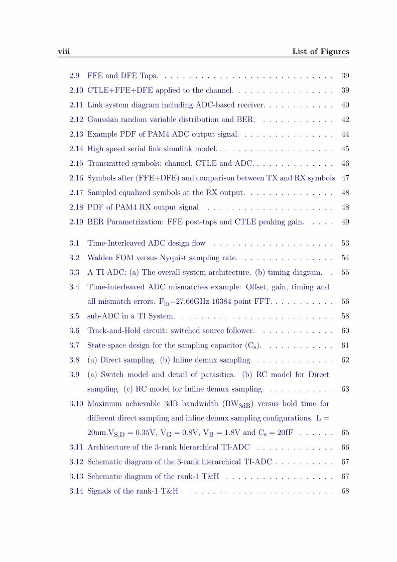
viii List of Figures
2.9 FFE and DFE Taps. . . . . . . . . . . . . . . . . . . . . . . . . . . . . 39
2.10 CTLE+FFE+DFE applied to the channel. . . . . . . . . . . . . . . . . 39
2.11 Link system diagram including ADC-based receiver. . . . . . . . . . . . 40
2.12 Gaussian random variable distribution and BER. . . . . . . . . . . . . 42
2.13 Example PDF of PAM4 ADC output signal. . . . . . . . . . . . . . . . 44
2.14 High speed serial link simulink model. . . . . . . . . . . . . . . . . . . . 45
2.15 Transmitted symbols: channel, CTLE and ADC. . . . . . . . . . . . . . 46
2.16 Symbols after (FFE+DFE) and comparison between TX and RX symbols. 47
2.17 Sampled equalized symbols at the RX output. . . . . . . . . . . . . . . 48
2.18 PDF of PAM4 RX output signal. . . . . . . . . . . . . . . . . . . . . . 48
2.19 BER Parametrization: FFE post-taps and CTLE peaking gain. . . . . 49
3.1 Time-Interleaved ADC design flow . . . . . . . . . . . . . . . . . . . . 53
3.2 Walden FOM versus Nyquist sampling rate. . . . . . . . . . . . . . . . 54
3.3 A TI-ADC: (a) The overall system architecture. (b) timing diagram. . 55
3.4 Time-interleaved ADC mismatches example: Offset, gain, timing and
all mismatch errors. Fin=27.66GHz 16384 point FFT. . . . . . . . . . . 56
3.5 sub-ADC in a TI System. . . . . . . . . . . . . . . . . . . . . . . . . . 58
3.6 Track-and-Hold circuit: switched source follower. . . . . . . . . . . . . 60
3.7 State-space design for the sampling capacitor (Cs). . . . . . . . . . . . 61
3.8 (a) Direct sampling. (b) Inline demux sampling. . . . . . . . . . . . . . 62
3.9 (a) Switch model and detail of parasitics. (b) RC model for Direct
sampling. (c) RC model for Inline demux sampling. . . . . . . . . . . . 63
3.10 Maximum achievable 3dB bandwidth (BW3dB) versus hold time for
different direct sampling and inline demux sampling configurations. L =
20nm,VS,D = 0.35V, VG = 0.8V, VB = 1.8V and Cs = 20fF . . . . . . 65
3.11 Architecture of the 3-rank hierarchical TI-ADC . . . . . . . . . . . . . 66
3.12 Schematic diagram of the 3-rank hierarchical TI-ADC . . . . . . . . . . 67
3.13 Schematic diagram of the rank-1 T&H . . . . . . . . . . . . . . . . . . 67
3.14 Signals of the rank-1 T&H . . . . . . . . . . . . . . . . . . . . . . . . . 68

List of Figures ix
3.15 (a) Rank-1 buffer: Source Follower. (b) Rank-2 buffer: Gain-boosted
Flipped Voltage Follower (FVF) . . . . . . . . . . . . . . . . . . . . . . 69
3.16 Signals of the rank-2 T&H . . . . . . . . . . . . . . . . . . . . . . . . . 70
3.17 (a) Diagram of the rank-3 gain stage. (b) Fully differential two-stage
OpAmp with gain enhancement. . . . . . . . . . . . . . . . . . . . . . . 71
3.18 Signals of the rank-3 T&H . . . . . . . . . . . . . . . . . . . . . . . . . 71
3.19 Normalized output variation between stages . . . . . . . . . . . . . . . 72
3.20 Hierarchical TH gain for nominal, slow and fast corners . . . . . . . . . 73
3.21 Diagram of the TI-ADC Clock generator . . . . . . . . . . . . . . . . . 74
3.22 (a) Input stage. (b) Buffer with DCD and delay calibration. . . . . . . 75
3.23 (a) FD8 with 12.5%DC. (b) FD4 with 25%DC. . . . . . . . . . . . . . . 76
3.24 Clock generator waveforms . . . . . . . . . . . . . . . . . . . . . . . . . 77
3.25 (a) Flash ADC. (b) SAR ADC with binary-weighted capacitive DAC. . 78
3.26 Energy comparison between SAR and Flash ADCs as a function of
resolution . . . . . . . . . . . . . . . . . . . . . . . . . . . . . . . . . . 80
3.27 (a) Architecture of the proposed single-channel 7-bit SAR ADC. (b)
LSB Capacitor Variation: LSB1 (red) and LSB2 (blue). (c) Layout. . . 81
3.28 LSB equivalent circuit with parasitics: (a) LSB1, (b) LSB2. (c) CPAR2
grid for a,b values . . . . . . . . . . . . . . . . . . . . . . . . . . . . . . 83
3.29 Strong ARM Comparator: (a) Schematic; (b) Layout . . . . . . . . . . 84
3.30 Histogram Strong ARM VOS: Uncalibrated; Calibrated for 100 MC runs 85
3.31 SAR Logic and timing . . . . . . . . . . . . . . . . . . . . . . . . . . . 87
3.32 sub-ADC power consumption breakdown. . . . . . . . . . . . . . . . . . 88
3.33 Histogram of ADC Output: Uncalibrated, Calibrated for 1000 MC runs 88
3.34 DNL and INL. LSB1 (red) and LSB2 (blue) . . . . . . . . . . . . . . . 89
3.35 Output Spectrum with 0 dBFS signal applied at 428.96 MHz, sampling
frequency is 875 MHz. LSB1 (red) and LSB2 (blue) . . . . . . . . . . . 90
3.36 Comparison with state-of-the-art single-channel SAR based on [2] . . . 91
3.37 Output Spectrum for the SAR-ADC model in simulink. . . . . . . . . . 94

x List of Figures
3.38 Output Spectrum for the TI-ADC model with mismatches. . . . . . . . 95
3.39 TI-ADC ENOB vs Non-linearity errors . . . . . . . . . . . . . . . . . . 96
3.40 TI-ADC power consumption breakdown. . . . . . . . . . . . . . . . . . 96
4.1 Diagram of 112 Gb/s PAM4 ADC-based receiver. . . . . . . . . . . . . 100
4.2 CTLE top diagram. . . . . . . . . . . . . . . . . . . . . . . . . . . . . 100
4.3 (a) 50Ω termination circuit. (b) Schematic diagram. . . . . . . . . . . . 101
4.4 CTLE transfer function for nominal, slow and fast corners . . . . . . . 103
4.5 Programmability of the peaking gain . . . . . . . . . . . . . . . . . . . 104
4.6 Programmability of the peaking frequency . . . . . . . . . . . . . . . . 104
4.7 (a) Direct retiming. (b) Indirect retiming for clock phase [3] . . . . . . 106
4.8 Retimer clock tree for 32x sub-ADCs. . . . . . . . . . . . . . . . . . . . 106
4.9 Timing Diagram of the Retimer. . . . . . . . . . . . . . . . . . . . . . . 107
4.10 CTLE layout. . . . . . . . . . . . . . . . . . . . . . . . . . . . . . . . . 108
4.11 TI-ADC Floorplanning. . . . . . . . . . . . . . . . . . . . . . . . . . . . 109
4.12 7-bit 56GS/s 64-Way TI-ADC layout. . . . . . . . . . . . . . . . . . . . 110
4.13 (a) Clock generator layout. (b) ADCs clock routing detail . . . . . . . 111
4.14 Chip layout. . . . . . . . . . . . . . . . . . . . . . . . . . . . . . . . . . 113
4.15 Prototype measurement set-up. . . . . . . . . . . . . . . . . . . . . . . 115
4.16 Modification of rank-1 to extend the design to 112GS/s . . . . . . . . . 116
4.17 A two-stage OpAmp with indirect feedback compensation using
split-length load devices. . . . . . . . . . . . . . . . . . . . . . . . . . . 117
4.18 Inverter configurations for different analog blocks. . . . . . . . . . . . . 118
4.19 Inverter-based single ended CTLE schematic. . . . . . . . . . . . . . . . 118
A.1 (a) Transconductance efficiency and (b) Current density (ID/W) for
the SLVT transistor. Wtotal = 10μm, L = 20nm, VDS = 0.4V and
VBS = 0.8V . . . . . . . . . . . . . . . . . . . . . . . . . . . . . . . . . 125
A.2 FOM vs gm/ID for the SLVT transistor. Wtotal = 10μm, L = 20nm,
VDS = 0.4V and VBS = 0.8V . . . . . . . . . . . . . . . . . . . . . . . 126
List of Figures xi
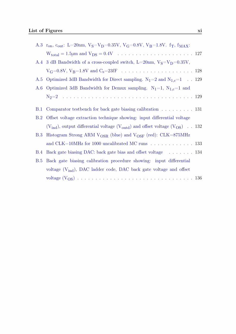
A.3 ron, cout: L=20nm, VS=VD=0.35V, VG=0.8V, VB=1.8V. fT, fMAX:
Wtotal = 1.5μm and VDS = 0.4V . . . . . . . . . . . . . . . . . . . . . 127
A.4 3 dB Bandwidth of a cross-coupled switch, L=20nm, VS=VD=0.35V,
VG=0.8V, VB=1.8V and Cs=23fF . . . . . . . . . . . . . . . . . . . . 128
A.5 Optimized 3dB Bandwidth for Direct sampling. N1=2 and N1,c=1 . . 129
A.6 Optimized 3dB Bandwidth for Demux sampling. N1=1, N1,c=1 and
N2=2 . . . . . . . . . . . . . . . . . . . . . . . . . . . . . . . . . . . . 129
B.1 Comparator testbench for back gate biasing calibration . . . . . . . . . 131
B.2 Offset voltage extraction technique showing: input differential voltage
(Vind), output differential voltage (Voutd) and offset voltage (VOS) . . 132
B.3 Histogram Strong ARM VOSR (blue) and VOSF (red): CLK=875MHz
and CLK=10MHz for 1000 uncalibrated MC runs . . . . . . . . . . . . 133
B.4 Back gate biasing DAC: back gate bias and offset voltage . . . . . . . 134
B.5 Back gate biasing calibration procedure showing: input differential
voltage (Vind), DAC ladder code, DAC back gate voltage and offset
voltage (VOS) . . . . . . . . . . . . . . . . . . . . . . . . . . . . . . . . 136
List of Tables
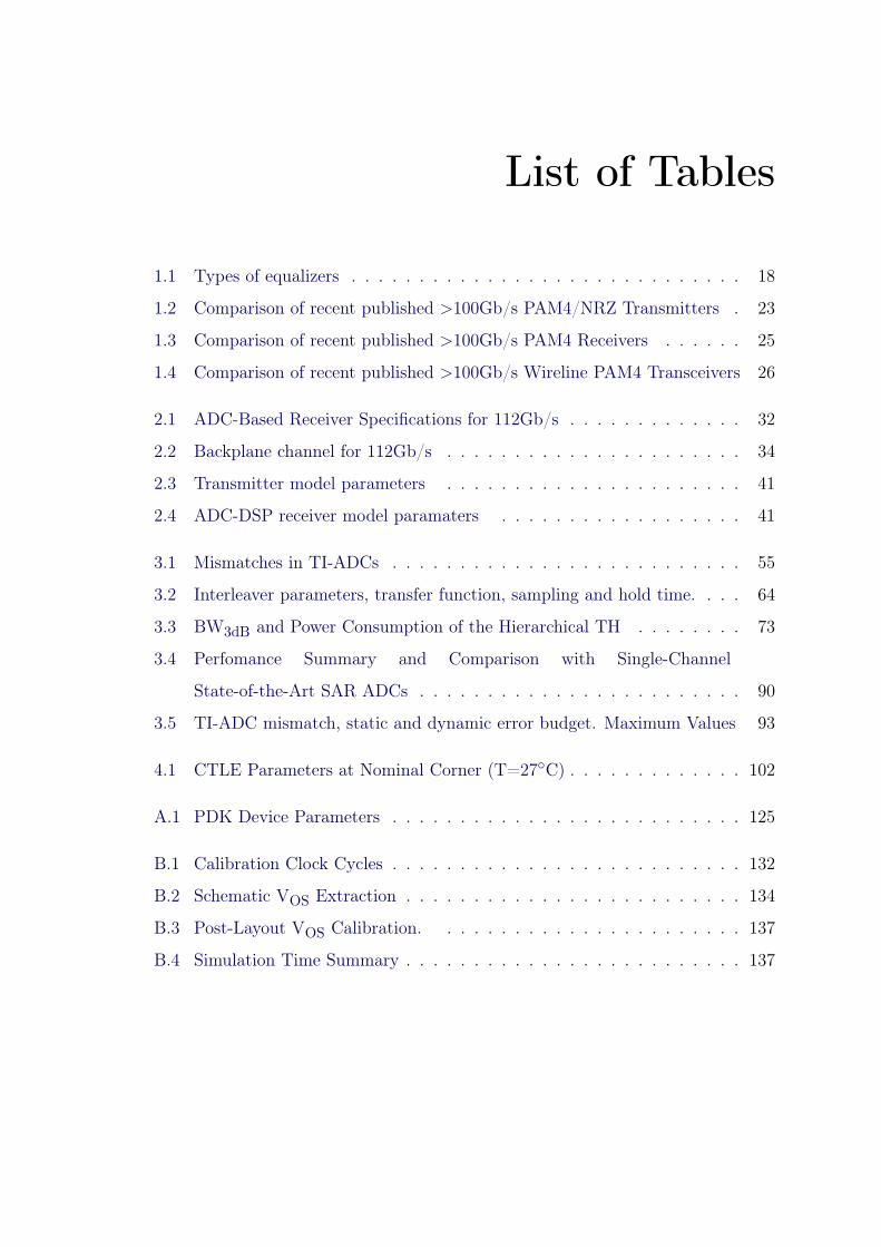
1.1 Types of equalizers . . . . . . . . . . . . . . . . . . . . . . . . . . . . . 18
1.2 Comparison of recent published >100Gb/s PAM4/NRZ Transmitters . 23
1.3 Comparison of recent published >100Gb/s PAM4 Receivers . . . . . . 25
1.4 Comparison of recent published >100Gb/s Wireline PAM4 Transceivers 26
2.1 ADC-Based Receiver Specifications for 112Gb/s . . . . . . . . . . . . . 32
2.2 Backplane channel for 112Gb/s . . . . . . . . . . . . . . . . . . . . . . 34
2.3 Transmitter model parameters . . . . . . . . . . . . . . . . . . . . . . 41
2.4 ADC-DSP receiver model paramaters . . . . . . . . . . . . . . . . . . 41
3.1 Mismatches in TI-ADCs . . . . . . . . . . . . . . . . . . . . . . . . . . 55
3.2 Interleaver parameters, transfer function, sampling and hold time. . . . 64
3.3 BW3dB and Power Consumption of the Hierarchical TH . . . . . . . . 73
3.4 Perfomance Summary and Comparison with Single-Channel
State-of-the-Art SAR ADCs . . . . . . . . . . . . . . . . . . . . . . . . 90
3.5 TI-ADC mismatch, static and dynamic error budget. Maximum Values 93
4.1 CTLE Parameters at Nominal Corner (T=27C) . . . . . . . . . . . . . 102
A.1 PDK Device Parameters . . . . . . . . . . . . . . . . . . . . . . . . . . 125
B.1 Calibration Clock Cycles . . . . . . . . . . . . . . . . . . . . . . . . . . 132
B.2 Schematic VOS Extraction . . . . . . . . . . . . . . . . . . . . . . . . . 134
B.3 Post-Layout VOS Calibration. . . . . . . . . . . . . . . . . . . . . . . 137
B.4 Simulation Time Summary . . . . . . . . . . . . . . . . . . . . . . . . . 137

List of Acronyms
ADC Analog-to-Digital Converter . . . . . . . . . . . . . . . . . . . . . . . . . 22
AFE Analog Front-End . . . . . . . . . . . . . . . . . . . . . . . . . . . . . . . 23
AGC Automatic Gain Control . . . . . . . . . . . . . . . . . . . . . . . . . . . 19
AI Artificial Intelligence . . . . . . . . . . . . . . . . . . . . . . . . . . . . . . 6
APMOM alternate-polarity metal-finger capacitors . . . . . . . . . . . . . . . 82
ATP Analog Test Point . . . . . . . . . . . . . . . . . . . . . . . . . . . . . . . 109
BER Bit Error Rate . . . . . . . . . . . . . . . . . . . . . . . . . . . . . . . . . 10
CAGR Compound Annual Growth Rate . . . . . . . . . . . . . . . . . . . . . 5
CDAC capacitive DAC . . . . . . . . . . . . . . . . . . . . . . . . . . . . . . . 80
CDR Clock Data Recovery . . . . . . . . . . . . . . . . . . . . . . . . . . . . . 14
CDF Cumulative Distribution Function . . . . . . . . . . . . . . . . . . . . . . 42
CMFB Common Mode Feedback . . . . . . . . . . . . . . . . . . . . . . . . . . 70
CML Current Mode Logic . . . . . . . . . . . . . . . . . . . . . . . . . . . . . 24
CPR Channel Pulse Response . . . . . . . . . . . . . . . . . . . . . . . . . . . 16
CTLE Continuous Time Linear Equalizer . . . . . . . . . . . . . . . . . . . . . 17
DAC Digital-to-Analog Converter . . . . . . . . . . . . . . . . . . . . . . . . . 23
DC Duty-Cycle . . . . . . . . . . . . . . . . . . . . . . . . . . . . . . . . . . . . 74
DCD Duty Cycle Distortion . . . . . . . . . . . . . . . . . . . . . . . . . . . . 74
DFE Decision Feedback Equalizer . . . . . . . . . . . . . . . . . . . . . . . . . 18

xiv List of Tables
DNL Differential Non-Linearity . . . . . . . . . . . . . . . . . . . . . . . . . . . 89
DSP Digital Signal Processing . . . . . . . . . . . . . . . . . . . . . . . . . . . 23
ENOB Effective Number Of Bits . . . . . . . . . . . . . . . . . . . . . . . . . . 58
EPON Ethernet Passive Optical Network . . . . . . . . . . . . . . . . . . . . . 6
FEC Forward Error Correction . . . . . . . . . . . . . . . . . . . . . . . . . . . 12
FFD Flip-Flop D . . . . . . . . . . . . . . . . . . . . . . . . . . . . . . . . . . . 76
FD4 Frequency Dividers by 4 . . . . . . . . . . . . . . . . . . . . . . . . . . . . 74
FD8 Frequency Divider by 8 . . . . . . . . . . . . . . . . . . . . . . . . . . . . 74
FFE FeedForward Equalizer . . . . . . . . . . . . . . . . . . . . . . . . . . . . . 17
FIR Finite-Impulse-Response . . . . . . . . . . . . . . . . . . . . . . . . . . . . 20
FOM Figure-Of-Merit . . . . . . . . . . . . . . . . . . . . . . . . . . . . . . . . 52
INL Integral Non-Linearity . . . . . . . . . . . . . . . . . . . . . . . . . . . . . 89
ISI InterSymbol Interference . . . . . . . . . . . . . . . . . . . . . . . . . . . . 7
ISR Interleaved Sampling Ratio . . . . . . . . . . . . . . . . . . . . . . . . . . 61
IL Insertion Loss . . . . . . . . . . . . . . . . . . . . . . . . . . . . . . . . . . . 14
LR Long Reach . . . . . . . . . . . . . . . . . . . . . . . . . . . . . . . . . . . . 15
LSB Least Significant Bit . . . . . . . . . . . . . . . . . . . . . . . . . . . . . . 80
MOM Metal-Oxide-Metal . . . . . . . . . . . . . . . . . . . . . . . . . . . . . . 75
NRZ Non-Return to Zero . . . . . . . . . . . . . . . . . . . . . . . . . . . . . . 7
PAM Pulse Amplitude Modulation . . . . . . . . . . . . . . . . . . . . . . . . . 7

List of Tables xv
PAM4 4-level Pulse Amplitude Modulation . . . . . . . . . . . . . . . . . . . . 10
PDF Probability Density Function . . . . . . . . . . . . . . . . . . . . . . . . . 42
PGA Programmable Gain Amplifier . . . . . . . . . . . . . . . . . . . . . . . . 27
PCB Printed Circuit Board . . . . . . . . . . . . . . . . . . . . . . . . . . . . . 7
PLL Phase-Locked Loop . . . . . . . . . . . . . . . . . . . . . . . . . . . . . . 13
POR Power-on-Reset . . . . . . . . . . . . . . . . . . . . . . . . . . . . . . . . 112
PRQS Pseudo Random Quaternary Sequence . . . . . . . . . . . . . . . . . . . 40
PVT Process Voltage Temperature . . . . . . . . . . . . . . . . . . . . . . . . . 61
RX Receiver . . . . . . . . . . . . . . . . . . . . . . . . . . . . . . . . . . . . . 7
RL Return Loss . . . . . . . . . . . . . . . . . . . . . . . . . . . . . . . . . . . 14
TX Transmitter . . . . . . . . . . . . . . . . . . . . . . . . . . . . . . . . . . . 7
SAR Successive Approximation Register . . . . . . . . . . . . . . . . . . . . . . 80
SER Symbol Error Rate . . . . . . . . . . . . . . . . . . . . . . . . . . . . . . . 43
SFDR Spurious Free Dynamic Range . . . . . . . . . . . . . . . . . . . . . . . 55
SNDR Signal-to-Noise-and-Distortion Ratio . . . . . . . . . . . . . . . . . . . . 55
SNR Signal-to-Noise Ratio . . . . . . . . . . . . . . . . . . . . . . . . . . . . . 10
SR-SAR Smart Resettable SAR . . . . . . . . . . . . . . . . . . . . . . . . . . 85
SST Source-Series Resistance . . . . . . . . . . . . . . . . . . . . . . . . . . . . 24
TG Transmission Gate . . . . . . . . . . . . . . . . . . . . . . . . . . . . . . . . 75
TH Track-and-Hold . . . . . . . . . . . . . . . . . . . . . . . . . . . . . . . . . 52

xvi List of Tables
TI Time-Interleaved . . . . . . . . . . . . . . . . . . . . . . . . . . . . . . . . . 52
TI-ADC Time-Interleaved ADC . . . . . . . . . . . . . . . . . . . . . . . . . . 25
VGA Variable Gain Amplifier . . . . . . . . . . . . . . . . . . . . . . . . . . . 26
UI Unit Interval . . . . . . . . . . . . . . . . . . . . . . . . . . . . . . . . . . . 16

Introduction
The increasing demand of higher data rates in datacenters has led to new
emerging standards (200 - 400G Ethernet and others) in wireline communications.
These standards will favored more sophisticated encoding schemes that require less
bandwidth such as the case of PAM4. PAM4 indicates pulse-amplitude modulation
with the "4" indicating four levels of pulse modulation. Its encoding uses 4 levels
and reduces the bandwidth by a factor of 2. But at the price to be harder to be
supported by purely analog solutions. So, a natural shift towards multi-level signaling
and mixed-signal architectures is expected.
ADC-based solutions give more opportunities for speed increase. They present
more robust solutions over channels with high losses (>20dB), because they can take
advantage of technology scaling and most of the equalization can be implemented in
the digital domain. Such ADCs are implemented using time-interleaving: identical
sub-ADCs multiplexed in time, operating in parallel to achieve a higher sampling rate.
Thus, research in this area is crucial for the next-generation of wireline
communication systems. Therefore, this thesis proposes the design of a PAM4
ADC-based receiver implementation with 112Gb/s data rate in 22nm CMOS FDSOI.
This manuscript is composed of four chapters and organized as follows.
Chapter 1 introduces the context of high-speed digital links operating at 100Gb/s.
Different aspects of wireline communications are revised such as 100 Gigabit Ethernet
Standard, signal modulation, channel and equalization techniques at 100Gb/s. Then,
a state-of-the-art analysis of wireline transmitters, receivers and transceivers is
performed in order to identify the architectural trends and performance metrics.
Finally, a set of requirements for silicon-based wireline receivers operating at 100Gb/s
are defined.
Chapter 2 proposes the system analysis of an ADC-based receiver. It begins with
listing the main specifications for 112Gb/s operation and choosing the appropriate
channel for Long Reach applications. Then, several of the previously equalization

techniques are performed using the impulse response of the channel to evaluate them.
Finally, an ADC-based receiver model is proposed and evaluated through system
simulation in MATLAB Simulink.
Chapter 3 describes the design of a of 56GSample/s Time-Interleaved ADC
(TI-ADC) for ADC-based wireline receivers. The first part describes the concept of
TI-ADCs, the state of the art and the design considerations. The second part covers
the design, clock generation and the simulation results.
Chapter 4 presents the physical implementation of an ADC-based receiver
prototype in 22nm CMOS FDSOI technology. It includes the TI-ADC developed
in chapter 3 and other blocks that complete the design. A testbench to perform
characterization of the receiver and several aspects to improve the current design are
discussed.

Chapter 1
High Speed Digital Links at100Gb/s
Contents1.1 Datacenters . . . . . . . . . . . . . . . . . . . . . . . . . . . . . . 4
1.2 100 Gigabit Ethernet Standard . . . . . . . . . . . . . . . . . . 8
1.2.1 PAM4 Signaling . . . . . . . . . . . . . . . . . . . . . . . . . . . 10
1.2.2 Channel at 100Gb/s . . . . . . . . . . . . . . . . . . . . . . . . . 13
1.2.3 Channel Equalization . . . . . . . . . . . . . . . . . . . . . . . . 16
1.3 Wireline Transceivers for 100Gb/s . . . . . . . . . . . . . . . . 22
1.3.1 Transmitter . . . . . . . . . . . . . . . . . . . . . . . . . . . . . . 23
1.3.2 Receiver . . . . . . . . . . . . . . . . . . . . . . . . . . . . . . . . 24
1.3.3 Transceivers . . . . . . . . . . . . . . . . . . . . . . . . . . . . . . 26
1.4 Conclusion . . . . . . . . . . . . . . . . . . . . . . . . . . . . . . . 28

4 Chapter 1. High Speed Digital Links at 100Gb/s
In this chapter, we introduced the context of high speed digital links operating at
100Gb/s. Different aspects of wireline communications are revised such as 100 Gigabit
Ethernet Standard, signal modulation, channel and equalization techniques at 100Gb/s.
Then, a state-of-the-art analysis of wireline transmitters, receivers and transceivers
is performed in order to identify the architectural trends and performance metrics.
Finally, a set of requirements for silicon-based wireline receivers operating at 100Gb/s
are defined.
1.1 Datacenters
Data centers are the backbone of today’s Internet and cloud-based services and
unprecedented quantity of data delivered in/between data-centers.
A data center is a collection of computing resources grouped together using
communication networks to host applications and store data (see an example in Figure
1.1). A typical data-center is modeled as a multi-layer hierarchical network with
thousands of low-cost commodity servers and switches as network nodes.
Figure 1.1: TierPoint datacenters.

1.1. Datacenters 5
Figure 1.2: Global IP Traffic Growth [1]
The increasing complexity and sophistication of datacenter applications demands
new features in the datacenter bandwidth and network. To further understand the
impact that different services and applications are having on bandwidth growth, it
is necessary to look at forecasted bandwidth growth. Figure 1.2 shows a forecast of
Global IP Traffic Growth for the 2017 to 2022 time period, which illustrates growth
from 122EB per month to 396EB1 per month for a 26% Compound Annual Growth
Rate (CAGR).
These requirements have led to considerable activity in the design and use of
low-latency specialized data center fabrics such as PCI-Express based backplane
interconnects, InfiniBand (IBA) [3], data center Ethernet [4].
Ethernet is a family of standards for communication over a physical media in
computer networks. It is the most common technology in local area networks (LAN)
and the working group IEEE 802.3 have released many standards since the first one
11EB = 1exabyte = 1018bytes

6 Chapter 1. High Speed Digital Links at 100Gb/s
Source: http://ethernetalliance.org/technology/2020-roadmap/
Figure 1.3: Ethernet Applications.
which was released in 1982.
The Ethernet Alliance roadmap traces Ethernet’s path from 10Mb/s through
present-day speeds of 1 to 400 gigabit Ethernet (GbE) and looks ahead to future
speeds achieving up to 1.6 terabits Ethernet (TbE) and beyond (Figure 1.3). Figure
1.4 shows the evolution of the Ethernet speeds and possible future speeds. The
forward-looking map also provides guidance into key underlying technologies current
and future interfaces and the numerous application spaces where Ethernet plays a
fundamental role [5].
Service providers have driven higher speed Ethernet solutions for decades. Router
connections, Ethernet Passive Optical Network (EPON), client side optics for optical
transport network (OTN) equipment and wired and wireless backhaul. In particular,
the 5G mobile deployment is driving dramatic increases in both fronthaul and backhaul
applications and continues to push Ethernet to higher rates and longer distances. The
global demand by consumers for video shows no signs of changing.
Cloud providers were the first to adopt 10GbE servers on a large scale in 2010
for hyperscale data centers. With voracious appetites for applications like Artificial

1.1. Datacenters 7
Source: http://ethernetalliance.org/technology/2020-roadmap/
Figure 1.4: Ethernet Roadmap: Path to 100GbE single lane.
Intelligence (AI) and Machine Learning, hyperscale servers have moved to 25GbE and
are transitioning to 50GbE and beyond. Unique networking architectures within these
warehouse scale data centers have driven multiple multimode and single-mode fiber
solutions at 100, 200 and 400GbE. The bandwidth demands of hyperscale data centers
and service providers continue to grow exponentially, in a similar direction that blurs
the lines between the two.
The ethernet standard as any wireline link over a typical communication channel
can be modeled as a system shown in Figure 1.5. The link consists of a Transmitter
(TX), a channel and a Receiver (RX). The data is sent by a transmitter through
the channel, which consists of the Printed Circuit Board (PCB) trace, connectors and
is recovered at the receiver. The data is conventionally encoded in pulse amplitudes
which is referred to as Pulse Amplitude Modulation (PAM). Encoding 1 bit per symbol
requires two amplitude levels and is referred to as Non-Return to Zero (NRZ) or PAM2.
For higher-rate transmissions, each pulse is substantially dispersed by the channel
and InterSymbol Interference (ISI) occurs. An example of this is shown in Figure 1.5.
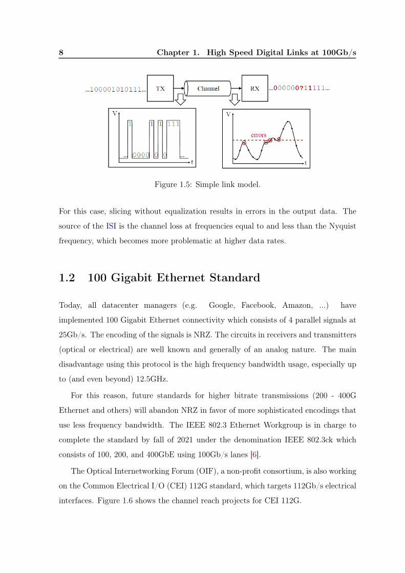
8 Chapter 1. High Speed Digital Links at 100Gb/s
Figure 1.5: Simple link model.
For this case, slicing without equalization results in errors in the output data. The
source of the ISI is the channel loss at frequencies equal to and less than the Nyquist
frequency, which becomes more problematic at higher data rates.
1.2 100 Gigabit Ethernet Standard
Today, all datacenter managers (e.g. Google, Facebook, Amazon, ...) have
implemented 100 Gigabit Ethernet connectivity which consists of 4 parallel signals at
25Gb/s. The encoding of the signals is NRZ. The circuits in receivers and transmitters
(optical or electrical) are well known and generally of an analog nature. The main
disadvantage using this protocol is the high frequency bandwidth usage, especially up
to (and even beyond) 12.5GHz.
For this reason, future standards for higher bitrate transmissions (200 - 400G
Ethernet and others) will abandon NRZ in favor of more sophisticated encodings that
use less frequency bandwidth. The IEEE 802.3 Ethernet Workgroup is in charge to
complete the standard by fall of 2021 under the denomination IEEE 802.3ck which
consists of 100, 200, and 400GbE using 100Gb/s lanes [6].
The Optical Internetworking Forum (OIF), a non-profit consortium, is also working
on the Common Electrical I/O (CEI) 112G standard, which targets 112Gb/s electrical
interfaces. Figure 1.6 shows the channel reach projects for CEI 112G.

1.2. 100 Gigabit Ethernet Standard 9
Source: https://www.oiforum.com/technical-work/current-work/
Figure 1.6: OIF’s Common Electrical I/O (CEI) 112G reach projects.
PolarizationModeDispersion(PMD)
Source: http://ethernetalliance.org/technology/2020-roadmap/
Figure 1.7: Data rate vs Parallelization for different modulation schemes.

10 Chapter 1. High Speed Digital Links at 100Gb/s
1.2.1 PAM4 Signaling
As data rate continues to increase, 112Gb/s over single lane is on the horizon.
The feasibility certainly depends on the choice of signal modulation and channel
characteristics. In this section, we provide a brief introduction to 4-level Pulse
Amplitude Modulation (PAM4) signaling so that basic concepts and ideas are defined.
Multi-level PAM is an emerging network signaling technology aimed to increase
data traffic throughput by reducing the signaling speed. As can be seen in Figure
1.7, data rate above 100Gb/s can be implemented by means of parallelization and
multi-level modulation.
PAM4 is gaining more attention in recent years as an alternative coding scheme to
NRZ (binary modulation Non Return to Zero). In NRZ signaling, one bit is a symbol
and has two distinct amplitude levels of ’0’ or ’1’. Symbols are expressed in terms of
baud. NRZ bitrate is equal to its symbol rate where 1Gb/s is equal to 1Gbaud.
PAM4 signaling uses four different levels, where each level corresponds to one
symbol representing two bits. With two bits per symbol, the baud rate is half the
bitrate. For example, 56Gbaud PAM4 is equal to 112Gbaud NRZ (112Gb/s). As
such, PAM4 achieves twice as much throughput using half the bandwidth compared
to NRZ. One of the most common naming convention for PAM4 signal levels is 0, 1,
2, 3, as can be seen in Figure 1.8.
In standard linear PAM4 signaling, it is possible for two transitions to happen at
the same time. These transitions can cause two-bit errors per symbol. If standard
PAM4 signaling is converted to gray code, the Bit Error Rate (BER) is reduced to
one-bit per symbol and the overall bit error rate is cut in half. BER can be expressed
as a function of the Signal-to-Noise Ratio (SNR) at the decision point:
BERM,levels =
(M – 1
2M
)× erfc
(√3 · SNR2(M2 – 1)
)(1.1)
where M is the number of distinct symbols for a given PAM modulation and erfc is
the complementary error function, [7].
Compared to NRZ’s two levels, PAM4 has four levels that result in 12 distinct

1.2. 100 Gigabit Ethernet Standard 11
Source: http://ethernetalliance.org/technology/2020-roadmap/
Figure 1.8: NRZ and PAM4 modulation schemes.
Figure 1.9: NRZ vs. PAM4 eye diagrams and symbols transition.
signal transitions. These transitions can be turned into an eye diagram (a.k.a. eye
pattern) by cutting it up into segments that are two bit (or symbol) intervals long and
overlaying them. An important advantage of the eye diagram over the linear signal

12 Chapter 1. High Speed Digital Links at 100Gb/s
representation is that it shows all possible bit transitions in a compact way, as shown
in Figure 1.9. From the eye diagram, it can be seen three distinct eye openings. Each
eye height is 1/3 of an NRZ eye height, causing the PAM4 SNR to be degraded by over
9.5dB, which has an impact to the signal quality and introduces additional constraints
in high-speed signaling.
As described above, the use of PAM4 signaling bring many advantages to overcome
the bandwidth limitations of NRZ, but also bring new challenges in link-path analysis.
New methodologies for PAM4 signaling have been developed in recent years, along with
IEEE standard amendments and commercial tools, in response to increasing demand
for higher speeds and the use of multi-level modulation schemes.
1.2.1.1 Forward Error Correction (FEC)
Forward Error Correction (FEC) is a method to control errors in transmitted data
over communication channels [8, 9]. Figure 1.10 shows FEC implementation. The
transmitted data is transformed into a codeword (redundant data addition) by the
FEC encoder, before passing through the channel. The added redundancy allows
the receiver FEC decoder to detect and correct errors that may occur. The general
disadvantage of FEC is that the transmitter will send the code to the receiver no
matter the code is correct or not, so a long and powerful error correction code is
required which leads to an inefficient use of channel.
In practice, sophisticated codes such as the Reed–Solomon (RS) codes and the
Bose–Chaudhuri–Hocquenghem (BCH) codes are used. In a typical transmission
Figure 1.10: Simplified system employing FEC.
1.2. 100 Gigabit Ethernet Standard 13
system with FEC, an incoming BER of 1×10⁻⁴ (i.e., BER at the output of the
receiver2) can be boosted to 1×10–12 (output BER or BERpost,FEC) after error
correction. This boosting means that a lower SNR requirement for the receiver can be
tolerated, while maintaining the same output BER.
FEC becomes an important part of a PAM4 system solution to offset this SNR
penalty, since one of the major design challenges of PAM4 signaling is the SNR penalty
of PAM4 over NRZ, about 9.54dB (1/3 of the available signal).
1.2.2 Channel at 100Gb/s
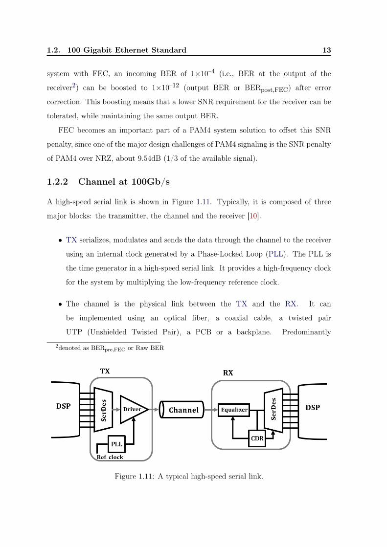
A high-speed serial link is shown in Figure 1.11. Typically, it is composed of three
major blocks: the transmitter, the channel and the receiver [10].
• TX serializes, modulates and sends the data through the channel to the receiver
using an internal clock generated by a Phase-Locked Loop (PLL). The PLL is
the time generator in a high-speed serial link. It provides a high-frequency clock
for the system by multiplying the low-frequency reference clock.
• The channel is the physical link between the TX and the RX. It can
be implemented using an optical fiber, a coaxial cable, a twisted pair
UTP (Unshielded Twisted Pair), a PCB or a backplane. Predominantly
2denoted as BERpre,FEC or Raw BER
Figure 1.11: A typical high-speed serial link.
14 Chapter 1. High Speed Digital Links at 100Gb/s
bandwidth-limited, the channel introduces loss, reflection and distortion in the
upcoming data.
• The RX recovers the upcoming data performing two operations: sampling the
input waveform with a clock synchronized with the data and deciding the digital
value of the sampled voltage. It is convenient to generate the clock inside the
receiver rather than transmit it from transmitter’s PLL on a separate channel.
The circuit that realizes this function is known as Clock Data Recovery (CDR).
A CDR circuit incorporates a PLL and some additional circuits needed to
synchronize the receiver with the incoming data stream. These timing blocks
are crucial parts in a high-speed system because they provide correct spacing
of transmitted data symbols and, on the receiver side, they have to sample the
received signal waveforms.
As data rates steadily rise, the signal integrity of the channel becomes critical in
high-speed serial link design. These signal integrity issues arise mostly due to the
channel-frequency-dependent characteristics. We can identify three major problems:
signal attenuation, reflection and crosstalk.
1. Signal attenuation occurs mostly due to conductor and dielectric losses. The
channel presents itself as low-pass, where the attenuation is proportional to
frequency. It can be characterized as the Insertion Loss (IL) of the channel.
2. The reflection is caused by impedance discontinuities or mismatches in the
channel and can significantly degrade the quality of the signal. Return Loss (RL)
is used to evaluate reflection.
3. Crosstalk occurs due to capacitive and inductive coupling between neighbouring
transmission channels. Depending on the crosstalk location and strength, it may
limit the signal transmission speed.
The combined effect of these problems creates attenuation and dispersion over the
high-frequency content of the transmitted symbols sent across the channel, resulting

1.2. 100 Gigabit Ethernet Standard 15
Figure 1.12: Insertion Loss (IL) for a channel intended for CEI-112G-LR.
in an attenuated received symbol energy that has been dispersed over several symbol
periods. When transmitting data across the channel, energy from individual symbols
will now interfere with adjacent ones and make them more difficult to detect. This ISI
increases with channel loss and can completely close the received data eye diagram.
As discussed above, operating at higher data rates makes the channel loss increasing
and the same channel technology may be unusable for higher throughput. Because
PAM4 has half the baud rate of a NRZ signal, the Nyquist frequency (FNYQ) in
PAM4 is half the FNYQ of NRZ for the same bitrate:
FNYQ,PAM4 = FNYQ,NRZ/2 = Fbitrate/4 (1.2)
The IL of a channel targeted for the CEI 112G Long Reach (LR) is shown in Figure
1.12. According to the specification the loss for 56GBaud PAM4 (112Gb/s) is between
28-30dB at Nyquist frequency of 28GHz. If NRZ were used instead of PAM4 for
the same speed, the loss would be more than 30dB making it unfeasible. This key

16 Chapter 1. High Speed Digital Links at 100Gb/s
advantage of PAM4 allows the use of existing channels and interconnects at higher
bitrates without the need for doubling the baud rate and increasing the channel
loss. Additionally, the impulse response can be obtained by taking the inverse Fourier
Transform of the insertion loss.
To evaluate signal integrity in serial link analysis, the single pulse response is often
used because:
• it gives a quick insight to the resulting eye diagram,
• it shows the effect of equalization,
• it gives insights to reflection and crosstalk,
• it helps characterize frequency-dependent loss of the channel.
Figure 1.13 shows the Channel Pulse Response (CPR). It is obtained by performing
the convolution of the impulse response with a pulse of width equal to the symbol
period. As can be seen the pulse energy is spread over several symbols Unit Interval
(UI)s. Typically the strongest response value is assigned as the cursor (UI=0 or current
UI), all the values before the cursor (UI<0) are called pre-cursors and the values
after (UI>0) post-cursors. The CPR is asymmetrical over time with a long tail and
dominated by post-cursors. This long tail is directly related to the low-frequency loss
typical of conductor losses.
The presence of ISI is detrimental to the reception of transmitted symbols, since it
tends to reduce the effective received SNR. Several ways to cancel or mitigate ISI will
be addressed in the following subsection.
1.2.3 Channel Equalization
In order to compensate the losses and distortion induced by the channel, a process
called equalization is employed [10, 11]. The purpose of the equalizer is to cancel
ISI and extend a given channel’s maximum data rate by making the cascade of the
channel and the equalizer have a flat frequency response, as shown in Figure 1.14. The

1.2. 100 Gigabit Ethernet Standard 17
Figure 1.13: Channel Pulse Response. ATX = 1Vpp, IL=30dB.
Figure 1.14: Channel Equalization in Frequency domain.
equalizer transfer function is the inverse of channel transfer function, i.e., a high pass
transfer function.
Depending on the application and maximum bit rate, we can distinguish three
types of equalizers:
1. Continuous Time Linear Equalizer (CTLE),
18 Chapter 1. High Speed Digital Links at 100Gb/s
2. FeedForward Equalizer (FFE),
3. Decision Feedback Equalizer (DFE),
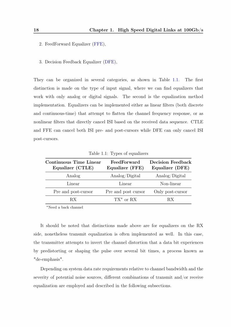
They can be organized in several categories, as shown in Table 1.1. The first
distinction is made on the type of input signal, where we can find equalizers that
work with only analog or digital signals. The second is the equalization method
implementation. Equalizers can be implemented either as linear filters (both discrete
and continuous-time) that attempt to flatten the channel frequency response, or as
nonlinear filters that directly cancel ISI based on the received data sequence. CTLE
and FFE can cancel both ISI pre- and post-cursors while DFE can only cancel ISI
post-cursors.
Table 1.1: Types of equalizers
Continuous Time Linear FeedForward Decision FeedbackEqualizer (CTLE) Equalizer (FFE) Equalizer (DFE)
Analog Analog/Digital Analog/Digital
Linear Linear Non-linear
Pre and post-cursor Pre and post cursor Only post-cursor
RX TX∗ or RX RX∗Need a back channel
It should be noted that distinctions made above are for equalizers on the RX
side, nonetheless transmit equalization is often implemented as well. In this case,
the transmitter attempts to invert the channel distortion that a data bit experiences
by predistorting or shaping the pulse over several bit times, a process known as
"de-emphasis".
Depending on system data rate requirements relative to channel bandwidth and the
severity of potential noise sources, different combinations of transmit and/or receive
equalization are employed and described in the following subsections.
1.2. 100 Gigabit Ethernet Standard 19
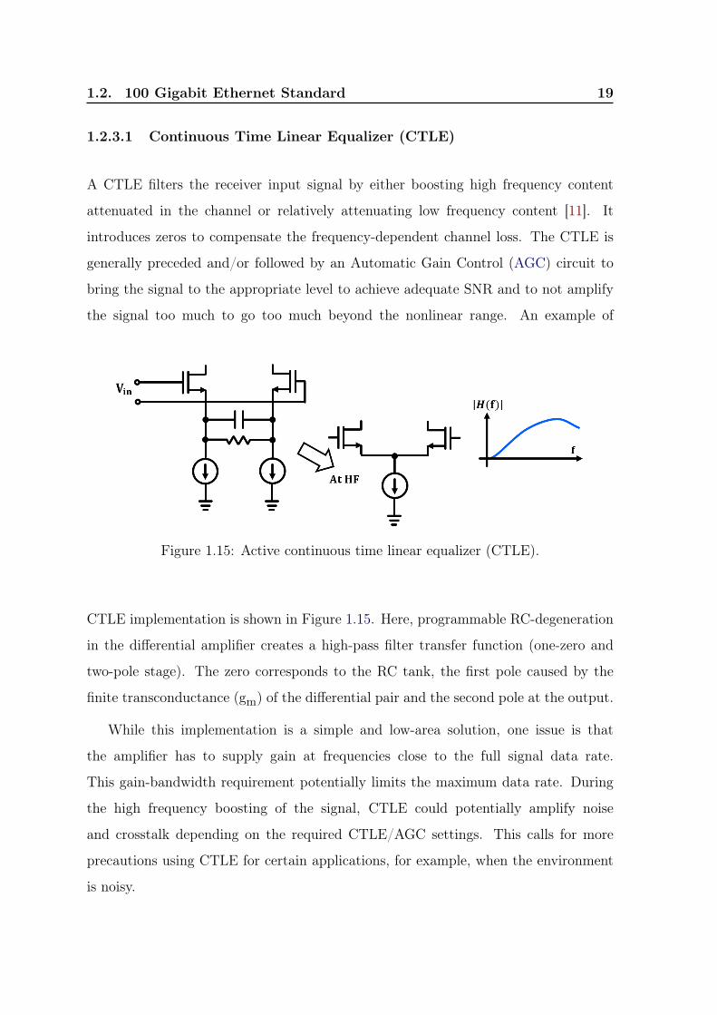
1.2.3.1 Continuous Time Linear Equalizer (CTLE)
A CTLE filters the receiver input signal by either boosting high frequency content
attenuated in the channel or relatively attenuating low frequency content [11]. It
introduces zeros to compensate the frequency-dependent channel loss. The CTLE is
generally preceded and/or followed by an Automatic Gain Control (AGC) circuit to
bring the signal to the appropriate level to achieve adequate SNR and to not amplify
the signal too much to go too much beyond the nonlinear range. An example of
Figure 1.15: Active continuous time linear equalizer (CTLE).
CTLE implementation is shown in Figure 1.15. Here, programmable RC-degeneration
in the differential amplifier creates a high-pass filter transfer function (one-zero and
two-pole stage). The zero corresponds to the RC tank, the first pole caused by the
finite transconductance (gm) of the differential pair and the second pole at the output.
While this implementation is a simple and low-area solution, one issue is that
the amplifier has to supply gain at frequencies close to the full signal data rate.
This gain-bandwidth requirement potentially limits the maximum data rate. During
the high frequency boosting of the signal, CTLE could potentially amplify noise
and crosstalk depending on the required CTLE/AGC settings. This calls for more
precautions using CTLE for certain applications, for example, when the environment
is noisy.

20 Chapter 1. High Speed Digital Links at 100Gb/s
1.2.3.2 FeedForward Equalizer (FFE)
The equalization capability required of time-domain equalizers in terms of number
of symbol-rate taps is directly proportional to the channel ISI delay spread and the
data rate. A FFE is implemented using a Finite-Impulse-Response (FIR) filter whose
function is to collect the energy from a set of ISI pre-cursors and post-cursors onto the
cursor [10, 11, 12].
(a) Implementation (b) 3-precursor/8-postcursor FFE
Figure 1.16: Feedforward equalizer (FFE)
A typical FFE implementation is shown in Figure 1.16. It consists of n multipliers
with a variable coefficient, n-1 delay cells and a summing node. A FIR can generate
large types of transfer function thanks to the different values of its coefficients. Usually,
since the signal input multipliers is taken along the delay line, the multipliers are called
"taps". The delays are interposed between the taps and each of them provides a delay
Td. In the time domain the input-output relation of the FIR is given as:
y(kT) =n∑
i=1
Wi(k + 1 – i)Td (1.3)
One method for determining the taps is to minimize the Mean Square Error (MSE) of
the equalizer output. We start calculating the error with respect to a desired output
E = HW – Ydes (1.4)

1.2. 100 Gigabit Ethernet Standard 21
where H represents the pulse response of the transmitted symbol and channel, W
corresponds to the FFE matrix taps and Ydes is the desired ISI free output. Then,
the error matrix norm2 is
‖E‖2 = WTHTHW – 2YTdesHW+YT
desYdes (1.5)
and differentiating with respect to the matrix taps, we find the taps which yield
minimum error norm2,
d
dW‖E‖2 = 2WTHTH – 2YT
desH
WTHTH = YTdesH
(1.6)
Finally solving for optimum FFE taps, leads to
Wopt = (HTH)–1HTYdes (1.7)
The matrix Wopt produces a value of "1" at the output cursor, so a normalization
by the sum of the absolute values of Wopt is needed:
Wopt,norm(n) =Wopt(n)∑n
i=1
∣∣Wopt(n)∣∣ (1.8)
A FFE may be programmed to mitigate ISI from all taps pre-cursor and
post-cursor. This can be achieved by implementing a FFE on the receiver-side and
adaptively tuning the filter taps to a specific channel. A disadvantage of the FFE
is the so-called noise enhancement [13]. For example, in trying to compensate for a
channel with a low-pass response, the equalizer adapts to a high-pass response, which
has the undesirable side effect of amplifying (or enhancing) high-frequency noise. The
result is a reduced SNR.
The problem of noise enhancement can be eliminated by using a DFE (Figure 1.17).
Unlike the aforementioned equalizers, DFE utilizes the previous decisions to estimate
and cancel the ISI introduced by the channel [10, 11, 12]. The feedback filter estimates
the ISI based on previous decisions and therefore, can only cancel post-cursor ISI. Since
the ISI cancellation is based on previous decisions, without high frequency boost, it
is inherently immune to noise enhancement. However, there is the potential for error
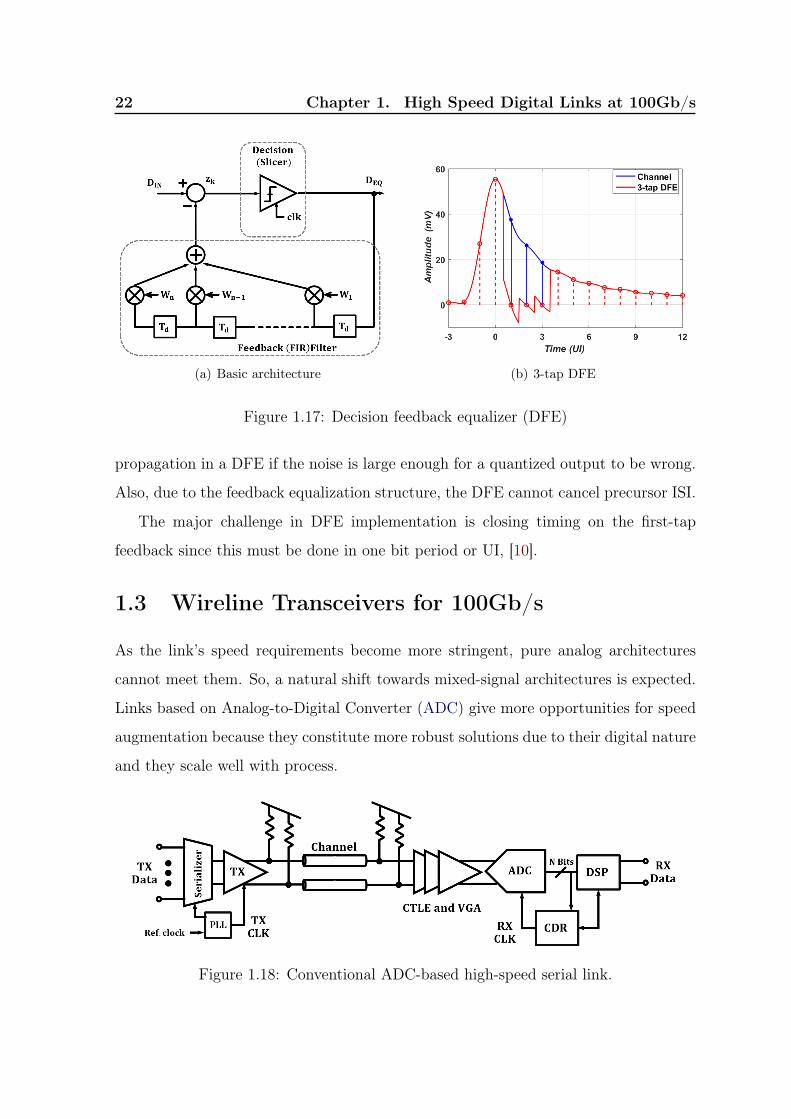
22 Chapter 1. High Speed Digital Links at 100Gb/s
(a) Basic architecture (b) 3-tap DFE
Figure 1.17: Decision feedback equalizer (DFE)
propagation in a DFE if the noise is large enough for a quantized output to be wrong.
Also, due to the feedback equalization structure, the DFE cannot cancel precursor ISI.
The major challenge in DFE implementation is closing timing on the first-tap
feedback since this must be done in one bit period or UI, [10].
1.3 Wireline Transceivers for 100Gb/s
As the link’s speed requirements become more stringent, pure analog architectures
cannot meet them. So, a natural shift towards mixed-signal architectures is expected.
Links based on Analog-to-Digital Converter (ADC) give more opportunities for speed
augmentation because they constitute more robust solutions due to their digital nature
and they scale well with process.
Figure 1.18: Conventional ADC-based high-speed serial link.

1.3. Wireline Transceivers for 100Gb/s 23
A typical ADC-based link is shown in Figure 1.18. Here, an Analog Front-End
(AFE) performs pre-equalization and signal conditioning for the input signal, then
ADC converts the pre-equalized signal into the digital domain. The Digital Signal
Processing (DSP) unit typically includes FFE and DFE. The CDR loop in the receiver
align the sampling clock with the received signal using a phase-tracking feedback loop.
In the following section, a review of the state-of-the-art of transmitters, receivers
and transceivers operating above 100Gb/s is presented.
1.3.1 Transmitter
Typically, three main categories of transmitters can be identify:
1. Analog or Digital-to-Analog Converter (DAC) based ones,
2. Architecture, the transmitter can be implemented full-rate or with serialization
(half-rate, quarter-rate),
Table 1.2: Comparison of recent published >100Gb/s PAM4/NRZ Transmitters
[14] [15] [16] [17] [18] [19] [20]
Conference VLSI ISSCC ISSCC ISSCC ISSCC ISSCC ISSCC2018 2018 2018 2019 2019 2020 2020
Architecture Quarter Quarter Quarter Quarter Quarter Half Quarterrate rate rate rate rate rate rate
Type Analog Analog DSP-DAC Analog Analog DSP-DAC DSP-DAC
Signaling PAM4 PAM4 PAM4 PAM4 PAM4 PAM4 NRZ/NRZ /NRZ /NRZ /NRZ
Technology 16nm 10nm 14nm 14nm 40nm 7nm 40nmFinFET CMOS CMOS FinFET CMOS FinFET CMOS
Data rate [Gb/s] 112 112 112 128 112 10-112 100
Clock On-chip On-chip External External On-chip On-chip ExternalSource PLL PLL PLL PLL
Driver SST CML SST CML SST Soft CMLTopology switching (tailless)
Output Swing 1Vpd 0.75Vpd 0.92Vpd 0.6Vpd 1Vpd 1.2Vpd 0.56Vpd
Tx FFE 4-tap FFE 3-tap 8-tap 3-tap FFE 4-tap 7-tap 8-tap
Efficiency [pJ/b]∗ 3.08 1.72 2.6 1 (112Gb/s) 3.62 1.05 6.19
Core Area [mm2] 0.38 0.0302 0.095 0.048 0.56 0.193 0.504∗Excluding PLL

24 Chapter 1. High Speed Digital Links at 100Gb/s
3. Output driver/combiner, it can be Current Mode Logic (CML) or Source-Series
Resistance (SST). For transmitters operating above 100Gb/s, a FFE of at
least 3-taps (pre-cursor, cursor and post-cursor) to compensate channel losses
is required.
Table 1.2 shows the state-of-the-art of 100Gb/s transmitters. A brief description
of these works pointing out their main characteristics follows.
Following the works in [14], [15], [17] and [18], we can find the classical or
analog-based Tx FFE structures. All analog implementations, with the exception
of [14], can support PAM4 and NRZ modulation. FFE tap reconfiguration is found
in [17] and [18]. In the latter, a two-step FFE consisting of coarse tuning and fine
tuning is adopted to overcome output bandwidth and power efficiency degradation.
DAC-based FFE structures are implemented in [16], [19], [20]. FFE is done in the
digital domain giving maximum flexibility and allowing a larger number of taps (> 7
taps).
All, with the exception of [19], employed quarter-rate architecture (clock frequency
≤ 16GHz) for power efficiency. For the driver topology, CML drivers are preferred for
DAC-based structures. In [19], a ‘soft-switching’ H-bridge output driver is introduced
to enable a 1.2V peak-to-peak differential output swing without exposing devices
beyond breakdown voltage.
Most of the transmitters have been implemented in technology node below 16nm.
The works presented in [18] and [20] aim to deliver PAM4 transmitters over 100Gb/s in
40nm CMOS to reduce costs. From this review, we can see that a trend for DAC-based
structures will be favored in the future, allowing more flexible designs.
1.3.2 Receiver
As mentioned earlier, the high logic density of lower process will allow receivers relying
heavily on digital signal processing (DSP), [21]. These digital receivers incorporate an
ADC to digitize the received signal and perform equalization in the digital domain.
The latest works for ADC-based receivers follow the same approach (see table 1.3).

1.3. Wireline Transceivers for 100Gb/s 25
Table 1.3: Comparison of recent published >100Gb/s PAM4 Receivers
[22] [23] [24]
Conference VLSI VLSI ISSCC2018 2019 2019
Architecture ADC-based ADC-based64-Way 64-Way Analog
7-bit SAR-ADC 6-bit SAR-ADC
Signaling PAM4 PAM4 PAM4/NRZ
Technology 16nm 10nm 14nmFinFET CMOS FinFET
Data rate [Gb/s] 112 112 100
Loss@Nyq. (dB) 20 (BERT) 35 (BERT) 19.2
Equalization CTLE CTLE 8-tap Tx FFE31-Tap FFE 16-Tap FFE CTLE1-tap DFE 1-tap DFE 1-tap DFE (1+0.5D)
Pre FEC BER 2×10⁻⁵ 1×10⁻⁶ < 1× 10–12
PRBS 31 31 15
CDR Baud rate Baud rate Baud rate (1+0.5D)
Efficiency [pJ/b]∗ 5.27 4.2 1.1
Core Area [mm2] 0.674 0.281 0.053∗Excluding DSP
An AFE, consisting of a CTLE and gain stage, provides a "pre-equalization" and
signal conditioning for a Time-Interleaved ADC (TI-ADC). The ADC samples are
retimed and sent to equalization, with DSP accounting a large number of FFE taps
and 1-tap DFE. In [22], a peaked source follower that uses programmable inductive
peaking compensates bandwidth losses before the ADC. The pre-DSP ADC outputs
are periodically stored in an on-chip 64Kb storage and read into an off-chip FPGA
that performs equalization adaptations and ADC offset/gain/skew calibrations. A
Q-shaping equalization in the CTLE is implemented in [23] for a tuning of 25dB gain
at peak frequency of 26GHz.
One important aspect to mention is the power consumption. Usually, these
ADC-based designs are power hungry reaching 500mW per lane without counting
the DSP power. A low-power alternative is presented [24], where the receiver uses a
CTLE combined with a 1-tap speculative DFE. Power optimization is obtained when
the number of slicing levels to resolve the 1-tap PAM4 DFE speculation is reduced

26 Chapter 1. High Speed Digital Links at 100Gb/s
Table 1.4: Comparison of recent published >100Gb/s Wireline PAM4 Transceivers
[25] [26] [27]
Conference ISSCC ISSCC ISSCC2019 2020 2020
Signaling PAM4/NRZ PAM4 PAM4
Technology 16nm 7nm 7nmFinFET FinFET FinFET
Data rate [Gb/s] 106 112 112
Loss@Nyq. (dB)/ BER DR4/FR4 optical 37.5@ BER=1× 10⁻⁸ 38.9@ BER< 5× 10⁻⁷
TX Arch. CML, 7-bit DAC CML, Analog SST, 7-bit DAC3-tap FIR 4-tap FIR 6-tap FIR
RX Arch. ADC-based ADC-based ADC-basedVGA CTLE/PGA CTLE/VGA
64-Way 36-Way 56-Way7-bit SAR-ADC 7-bit SAR-ADC 7-bit SAR-ADCDSP: 10 FFE DSP: 31 FFE/1-DFE DSP: 8-24 FFE/1-DFE
Power∗ [mW/lane] 900 602 460
Core Area [mm2] 1.54 0.403 0.385∗Excluding DSP
from 12 to 8 by shaping the channel to a 1+0.5D response (h0+0.5*h0) with CTLE
and Tx FFE. This receiver design can equalize a 19.2dB loss channel (with 8-tap TX
FFE) while consuming 111.4mW at 100Gb/s PAM4 signaling. It can be seen that for
channels with medium losses (<20dB), an analog solution presents itself as a good
alternative for power saving.
1.3.3 Transceivers
We have reviewed transmitters and receivers as standalone building blocks, but
ultimately both will interact with each other inside the link. Three designs operating
above 100Gb/s are described, one for optical interconnections and the other two for
electrical ones (Table 1.4). In terms of architecture, all receivers are ADC-based and
all transmitters are analog and DAC-based, both with FFE.
A transceiver for PAM4 optical interconnections is presented in [25]. The
transmitter is dual mode PAM4/NRZ DAC-based 3-tap FIR with half-rate
architecture. The pre-driver adopts a resistor feedback inverter topology for a sub-UI
equalizer to improve bandwidth and ISI. The receiver is composed of Variable Gain

1.3. Wireline Transceivers for 100Gb/s 27
Amplifier (VGA) followed by a 64-way 7-bit SAR-ADC. The ADC uses a 2-rank
hierarchical time-interleaved sampling architecture to reduce the VGA load and the
number of jitter-critical clock signals. It is fabricated in 16nm FinFET and consumes
900mW.
The transceivers for electrical connections share similar characteristics. Both are
designed for LR with channel losses >30dB with ADC-based architecture in the
receiver and DSP for FFE/DFE equalization. They are fabricated in 7nm FinFET.
A CML 4-tap FFE analog transmitter operating at quarter-rate is presented in
[26]. It implements duty cycle and I/Q mismatch calibration to enable the use of a
power-efficient CMOS 4:1 MUX. A distributed inductor peaking network is designed
to compensate for >200fF device and parasitic capacitance at the current summing
node. The AFE consists of a 2-stage CTLE and Programmable Gain Amplifier (PGA),
both using inverter-based amplifier stages comprised of a Gm cell and inverse-Gm load
(Gml). The ADC is a 36-way TI-ADC, operating 6-by-6 sub-ADC units in a two-rank
hierarchy. The DSP implements a 31-tap FFE and 1-tap DFE. This transceiver
achieves a BER lower than < 1× 10⁻⁸ for a channel loss of 37.59dB.
A SST 6-tap DAC-based transmitter is presented in [27]. A Gm-TIA-based
topology is used for the CTLE and VGA. The ADC is a 56-way TI-ADC with 8-way
T/H sampler to simplify clocking complexity, provide isolation between consecutive
T/H phases and reduces CTLE loading. The DSP implements a programmable 8-24
tap FFE with a 1-tap, loop-unrolled DFE equalizer. DSP also includes a 6-tap FIR
in the Tx side for de-emphasis. It is able to achieve a BER better than 5× 10⁻⁷ with
38.9dB channel loss while consuming 460mW (TX/RX w/o DSP), the lowest power
reported for 112Gb/s PAM4 LR applications.

28 Chapter 1. High Speed Digital Links at 100Gb/s
1.4 Conclusion
This chapter has introduced the context of high speed digital links, from the
current standard to equalization techniques for 100Gb/s applications. Following
the state-of-the-art analysis, it seems to guarantee single lane operation at 100Gb/s
and beyond. The link modules (transmitter and receiver) should meet the following
requirements:
• Multi-level signaling capabilities, to enable an efficient usage of bandwidth,
• Mixed signal architecture, to take advantage of technology scaling and
implement most of the equalization in the digital domain,
• Low-power operation, to cope with energy and power dissipation constraints.
DAC-based transmitters and ADC-based receivers appear as good candidates to
provide a 100Gb/s solution. The realization of a suitable receiver that meets the
requirements listed above will be conducted in the next chapter.
We propose to validate through a link system analysis, the specifications
of an ADC-based receiver compatible with 100Gb/s operation.

Chapter 2
A Wireline PAM4 ADC-BasedReceiver for 112Gb/s
Contents2.1 Link System Level methodology . . . . . . . . . . . . . . . . . . 30
2.2 Receiver specifications . . . . . . . . . . . . . . . . . . . . . . . 32
2.2.1 Channel selection . . . . . . . . . . . . . . . . . . . . . . . . . . . 34
2.3 Channel Equalization at 100Gb/s . . . . . . . . . . . . . . . . . 36
2.3.1 CTLE . . . . . . . . . . . . . . . . . . . . . . . . . . . . . . . . . 37
2.3.2 FFE and DFE . . . . . . . . . . . . . . . . . . . . . . . . . . . . 38
2.4 Link System Simulation . . . . . . . . . . . . . . . . . . . . . . . 40
2.4.1 Link Description . . . . . . . . . . . . . . . . . . . . . . . . . . . 40
2.4.2 PAM4 BER calculation based on PDF estimation . . . . . . . . . 42
2.4.3 Simulation results . . . . . . . . . . . . . . . . . . . . . . . . . . 45
2.5 Conclusion . . . . . . . . . . . . . . . . . . . . . . . . . . . . . . . 50

30 Chapter 2. A Wireline PAM4 ADC-Based Receiver for 112Gb/s
In this chapter, the system analysis of an ADC-based receiver is implemented. It
begins with listing the main specifications for 112Gb/s operation and choosing the
appropriate channel for Long Reach applications. Then, several of the previously
reviewed equalization techniques are performed using the impulse response of the
channel to evaluate them. Finally, an ADC-based receiver model is proposed and
evaluated through system simulations in MATLAB Simulink.
2.1 Link System Level methodology
A link system analysis is performed to evaluate the specifications of a wireline receiver
that complies with 112Gb/s operation for Long Reach applications. Figure 2.1 presents
the methodology used for the link system simulation. It is described as follows:
• An analysis of the 100GbE standard and state-of-art of wireline receivers is
carried out to define the specifications and architecture,
• The channel is selected according to the IL requirements for LR applications,
• The IL, ICN and CPR are extracted from the S-paramater files of the selected
channel,
• Equalization is applied to the CPR to obtain the CTLE transfer function and
FFE/DFE coefficients,
• The link is built in MATLAB Simulink using the IL, ICN and CPR equalization.
The model includes: transmitter, channel, receiver and crosstalk,
• Both transmitter (TX) and receiver (RX) are parameterized for more flexible
analysis,
• The link is simulated for a given set of Tx/Rx parameters and bit pattern. Then,
the BER is calculated from the received bit pattern,
• This simulation is repeated if there is a new set of parameters.
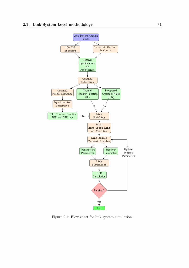
2.1. Link System Level methodology 31
Link System Analysisstarts
100 GbE
Standard
State-of-the-art
Analysis
ReceiverSpecifications
andArchitecture
Channel
Selection
ChannelTransfer Function
(IL)
IntegratedCrosstalk Noise
(ICN)
Channel
Pulse Response
Equalization
Tecniques
CTLE Transfer FunctionFFE and DFE taps
Link
Modeling
Built
High Speed Link
on Simulink
Link Module
Parametrization
TransmittersParameters
ReceiverParameters
Link
Simulation
BERCalculation
Finished?
End
yesyes
to to
to
no:UpdateModule
Parameters
Figure 2.1: Flow chart for link system simulation.

32 Chapter 2. A Wireline PAM4 ADC-Based Receiver for 112Gb/s
2.2 Receiver specifications
A set of specifications for an ADC-based receiver that complies with 112Gb/s operation
for Long Reach applications is proposed in Table 2.1. These specifications were based
on the 100GbE standard and the state-of-the-art wireline receivers.
Table 2.1: ADC-Based Receiver Specifications for112Gb/s
Specifications
Data rate [Gb/s] 112
Baud rate [Gbd] 56
Signaling PAM4
FNyquist [GHz] 28
IL [dB] ∼20dB to ∼30dB @ FNyquist
BER Raw: 1×10⁻⁴ to 1×10⁻⁵,Using FEC: 1×10–12
Power∗ [mW/lane] < 500∗Excluding DSP
The most important features for this receiver are:
1. The use of PAM4 modulation. PAM4 signaling presents a good alternative over
NRZ in terms of bandwidth efficiency,
2. The receiver is intended to compensate losses above 20dB to make it suitable for
Long Reach applications,
3. The use of PAM4 signaling. It requires the use of FEC-encoding in order to
relax the specifications of the receiver. A raw BER (no FEC) between [1×10⁻⁴
- 1×10⁻⁵] is set as a constraint. FEC-enconding will reduce BER to a more
suitable value of 1×10–12, expected for high-speed serial links,
4. The receiver is competitive with current state-of-the-art implementations. A
power target of 500mW is defined, which corresponds to the analog/mixed-signal
blocks of the receiver with the exception of DSP.
2.2. Receiver specifications 33
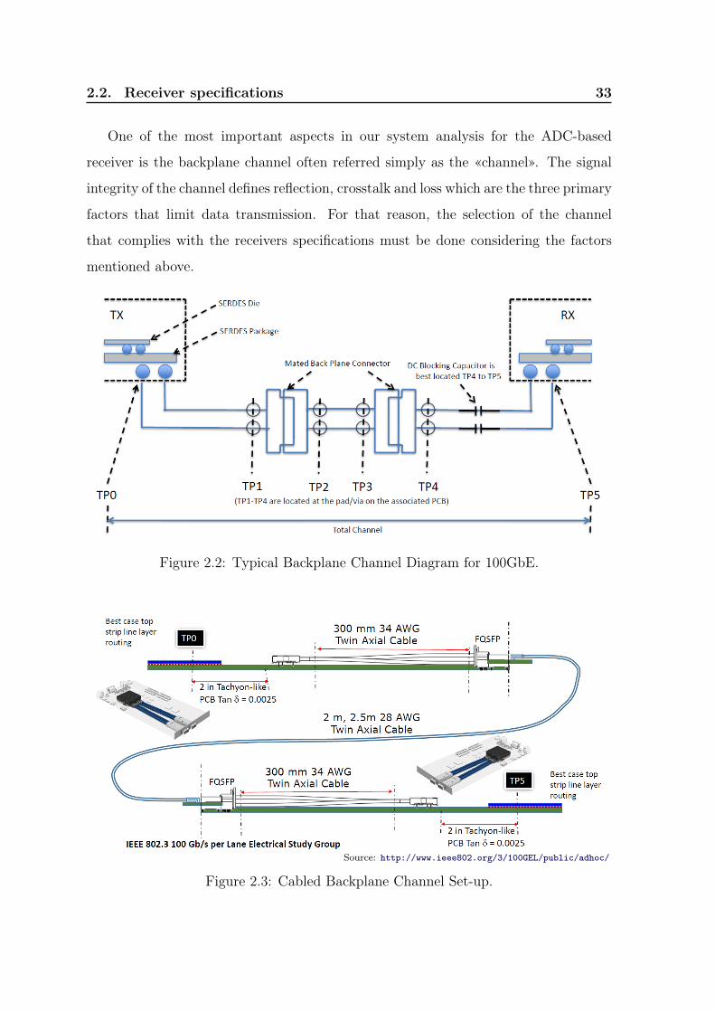
One of the most important aspects in our system analysis for the ADC-based
receiver is the backplane channel often referred simply as the «channel». The signal
integrity of the channel defines reflection, crosstalk and loss which are the three primary
factors that limit data transmission. For that reason, the selection of the channel
that complies with the receivers specifications must be done considering the factors
mentioned above.
Figure 2.2: Typical Backplane Channel Diagram for 100GbE.
Source: http://www.ieee802.org/3/100GEL/public/adhoc/
Figure 2.3: Cabled Backplane Channel Set-up.

34 Chapter 2. A Wireline PAM4 ADC-Based Receiver for 112Gb/s
Figure 2.2 shows a typical point-to-point channel topology with cable assembly.
The channel comprises the connection between the TX and RX packages (TP0 to
TP5). The test point (TP) is the reference point used for the IL budget breakdown.
All the losses between TP0 and TP5, due to connectors and cables, are taken into
account for the channel IL. A backplane channel configuration is presented in Figure
2.3. This configuration is known as «cabled backplane». It presents lower losses
compared to the traditional PCB backplane channel at high frequencies, making it
suitable for 112Gb/s operation.
2.2.1 Channel selection
Following the receiver specifications, a channel was chosen to meet the IL constraint
at the Nyquist Frequency. Three backplane channels proposed by the IEEE P802.3ck
Task Force [6] have been listed in Table 2.2. An orthogonal backplane channel has
been added for comparison between the cabled ones. The IL and ICN were calculated
using the S-parameters files for a 4-port model. This file is a cascaded form of the
different interconnections through the channel. The ICN represents the impact due to
both near-end (NEXT) and far-end (FEXT) crosstalk.
The package must be added to complete the backplane channel model. The
electrical parameters of the package must achieve stringent requirements in order
to support high-speed signals. For that reason, a flexible package model with LC
termination compensation has been proposed by the IEEE P802.3ck Task Force.
Table 2.2: Backplane channel for 112Gb/s
Channel Characteristics Configuration IL FEXT ICN@ FNyquist NEXT
1 (1.92mm) micro via TP0, TP5 Cabled 28.3dB 5/3 0.69mV92.5Ω 30AWG: 30mm, 1m
2 24" PCB Megtron-7N Orthogonal 30.7dB 5/3 0.38mVSTRADA Whisper Conn.
3 30AWG Flyover line: 30mm Cabled 29.5dB 3/4 1.55mV28AWG: 2m

2.2. Receiver specifications 35
DieRd=45
Cd=120fF
Ls=120pH
Cb=30fF
TP0
Cp=87fF
Zc=87.5Ω
Zp=12, 31/29mm
Zc1=92.5Ω
Zp1=1.8mm
Figure 2.4: Package model.
A single-sided model is presented in Figure 2.4 and will be cascaded with the
S-parameters file of the channel. To finalize, a “fitted curve” (up to half of bandwidth,
i.e. Nyquist rate) is introduced to approximate the IL as a linear transfer function that
will be used in MATLAB. Figure 2.5 shows the insertion loss for the three channels
including the fitted version and package. We have chosen the third configuration for
our system analysis, as it is the one that presents itself as the most challenging to
equalize.
Figure 2.5: Insertion Loss for 3 different configuration channels.

36 Chapter 2. A Wireline PAM4 ADC-Based Receiver for 112Gb/s
2.3 Channel Equalization at 100Gb/s
After selecting the channel and extracting the pulse response, equalization is evaluated
using the techniques described in subsection 1.2.3. Figure 2.6 shows conventional
mixed-signal equalization blocks on both the TX and RX. The main cursor in
a channel’s pulse response is the signal of interest. A FFE, which is typically
implemented on the TX side, normally cancels pre-cursors. The post-cursors are often
taken care of by the receiver with a CTLE and DFE. The CTLE acts as high-pass
filter to compensate for the channel’s low-pass action. Due to the high-pass nature of
CTLEs, any high frequency receiver input noise will be boosted similar to the actual
signal. To avoid excessive noise amplification, DFEs pass the noise-less recovered bits
through a FIR filter that matches the post-cursor portions of the channel to achieve ISI
cancellation. The TX FFE can also provide some coarse equalization for post-cursors.
As both the links’ speed and area requirements become more stringent,
mixed-signal architectures pose significant implementation challenges. Specifically,
the CTLE and the DFE’s summing node are the bottlenecks.
TX Channel RX
inz−1 . . . z−1
out
FFE
inCTLE −
FIR
out
CTLE+DFE
Main cursor
Pre-cursors Post-cursors
Figure 2.6: Typical equalization scheme for mixed-signal links.

2.3. Channel Equalization at 100Gb/s 37
2.3.1 CTLE
The first technique evaluated is the CTLE. Eq. 2.1 presents the transfer function of
the CTLE. It consists of a three-poles/two-zeros system.
HCTLE(s) = AAGC · prefactor ·(s + ωZ1)
(s + ωP1)(s + ωP2
)·(s + ωZLF)
(s + ωPLF)
prefactor =P1P2PLF
Z1ZLF
(2.1)
where AAGC is the gain for automatic gain control (AGC) stage, ωP1, ωP2
, ωZ1 are the
high frequency two-poles/one-zero that gives the characteristic boost in Nyquist, ωPLF
and ωZLF is the low frequency pole/zero pair and its function is to reduce long-tail
ISI. Figure 2.7 shows the peaking gain at the Nyquist frequency for the CTLE transfer
function. The poles and zeros were normalized to the baud frequency (bd=56GHz).The
AGC was set 0.6 (-4.43dB) to avoid saturation at the input of the ADC. For a CTLE
bandwidth≈ p2,norm= [0.5-0.6]*bd, a peaking gain between [11-21]dB can be achieved.
The CPR with CTLE and transfer function are shown in Figure 2.8. A peak gain
of 18.45dB was applied. From the equalized pulse, the suppression of the post-cursors
Figure 2.7: CTLE peaking gain at Nyquist: Design space.
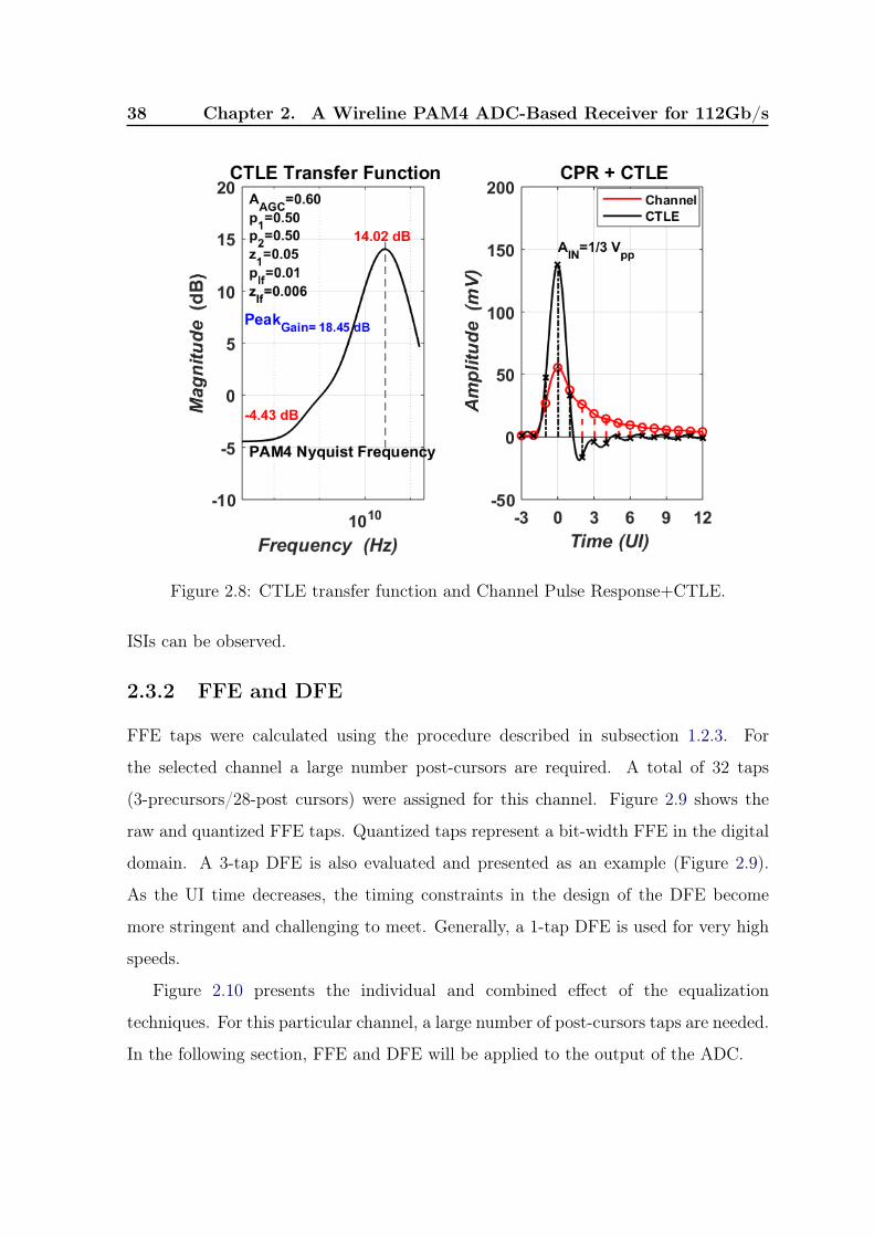
38 Chapter 2. A Wireline PAM4 ADC-Based Receiver for 112Gb/s
Figure 2.8: CTLE transfer function and Channel Pulse Response+CTLE.
ISIs can be observed.
2.3.2 FFE and DFE
FFE taps were calculated using the procedure described in subsection 1.2.3. For
the selected channel a large number post-cursors are required. A total of 32 taps
(3-precursors/28-post cursors) were assigned for this channel. Figure 2.9 shows the
raw and quantized FFE taps. Quantized taps represent a bit-width FFE in the digital
domain. A 3-tap DFE is also evaluated and presented as an example (Figure 2.9).
As the UI time decreases, the timing constraints in the design of the DFE become
more stringent and challenging to meet. Generally, a 1-tap DFE is used for very high
speeds.
Figure 2.10 presents the individual and combined effect of the equalization
techniques. For this particular channel, a large number of post-cursors taps are needed.
In the following section, FFE and DFE will be applied to the output of the ADC.

2.3. Channel Equalization at 100Gb/s 39
Figure 2.9: FFE and DFE Taps.
Figure 2.10: CTLE+FFE+DFE applied to the channel.

40 Chapter 2. A Wireline PAM4 ADC-Based Receiver for 112Gb/s
2.4 Link System Simulation
2.4.1 Link Description
Figure 2.11: Link system diagram including ADC-based receiver.
After defining the specifications for the receiver and selecting the backplane
channel, we proceeded to the link simulation in MATLAB Simulink. Figure 2.11
shows the link system diagram, which consists of the following:
• The transmitter (TX): in charge to generate the PAM4 symbols. A Pseudo
Random Quaternary Sequence (PRQS) generator using Gray coding was
implemented. Additionally, a 3-tap FIR filter was added for de-emphasis. Table
2.3 summarizes the TX parameters.
• The channel (CH): Represented as a rational function extracted from the
S-parameters file of channel 3 (Table 2.2) including package.
• Crosstalk (XT): A noise source (ICN) that represents the impact due to both
near-end and far-end crosstalk.
• The receiver (RX): A mixed-signal receiver. A CTLE and ADC represent the
analog part. Including the noise based on the one-sided spectral density η0
referred to the CTLE transfer function filter, quantization noise and jitter for
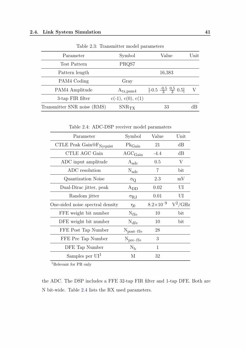
2.4. Link System Simulation 41
Table 2.3: Transmitter model parameters
Parameter Symbol Value Unit
Test Pattern PRQS7
Pattern length 16,383
PAM4 Coding Gray
PAM4 Amplitude Atx,pam4 [-0.5 –0.53
0.53 0.5] V
3-tap FIR filter c(-1), c(0), c(1)
Transmitter SNR noise (RMS) SNRTX 33 dB
Table 2.4: ADC-DSP receiver model paramaters
Parameter Symbol Value Unit
CTLE Peak Gain@FNyquist PkGain 21 dB
CTLE AGC Gain AGCGain -4.4 dB
ADC input amplitude Aadc 0.5 V
ADC resolution Nadc 7 bit
Quantization Noise σQ 2.3 mV
Dual-Dirac jitter, peak ADD 0.02 UI
Random jitter σRJ 0.01 UI
One-sided noise spectral density η0 8.2×10⁻⁹ V2/GHz
FFE weight bit number Nffe 10 bit
DFE weight bit number Ndfe 10 bit
FFE Post Tap Number Npost–ffe 28
FFE Pre Tap Number Npre–ffe 3
DFE Tap Number Nb 1
Samples per UI1 M 321Relevant for PR only
the ADC. The DSP includes a FFE 32-tap FIR filter and 1-tap DFE. Both are
N bit-wide. Table 2.4 lists the RX used parameters.

42 Chapter 2. A Wireline PAM4 ADC-Based Receiver for 112Gb/s
2.4.2 PAM4 BER calculation based on PDF estimation
The BER is used to evaluate the link’s performance. To calculate the BER, we start
with a Gaussian random variable (X) that has a Probability Density Function (PDF)
defined by
pX(x) =1
σ√2π
e–12 (
x–μσ
)2 (2.2)
where μ and σ are the mean offset and variance, respectively. X represents a detected
symbol (or bit) μ with a certain noise power σ. Figure 2.12 shows X distribution. A
is the lower threshold that gives the probability of a right symbol detection. The area
denoted by x≤A represents the probability error P(x≤A) or BER, to make a wrong
symbol detection.
P(x≤A) can be calculated using the Cumulative Distribution Function (CDF)
A x
f(x)
,
BER
Figure 2.12: Gaussian random variable distribution and BER.
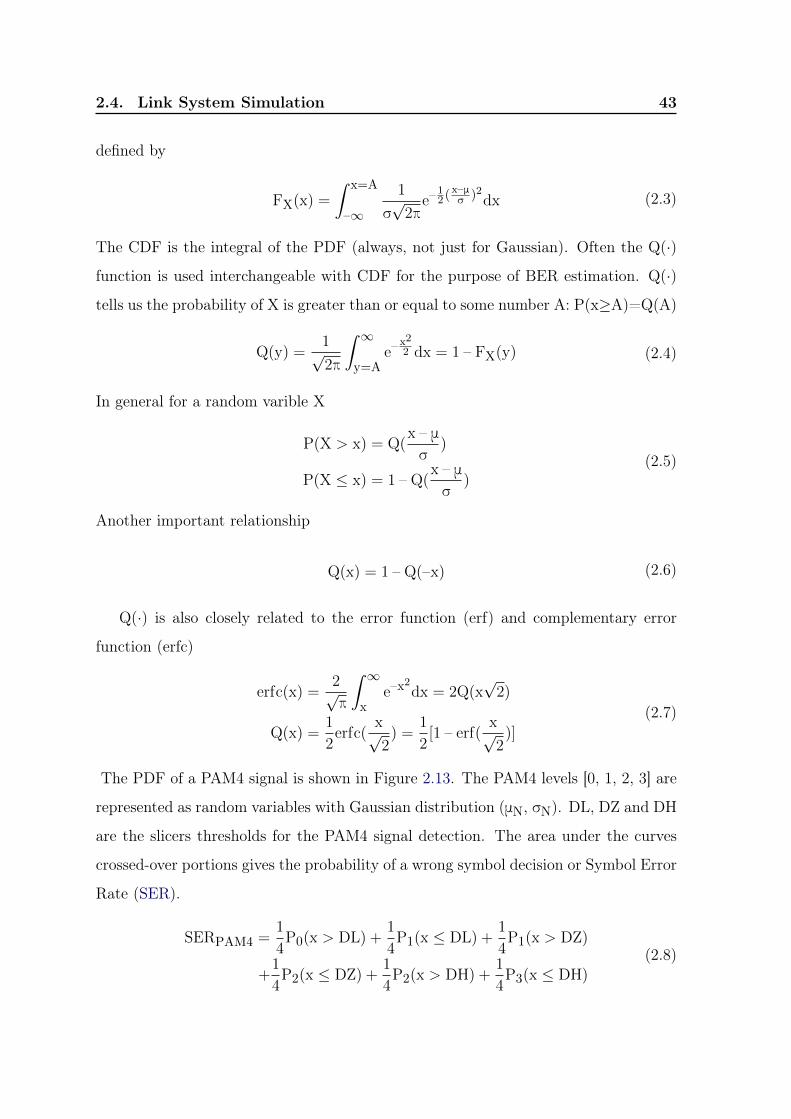
2.4. Link System Simulation 43
defined by
FX(x) =
∫ x=A
–∞1
σ√2π
e–12 (
x–μσ
)2dx (2.3)
The CDF is the integral of the PDF (always, not just for Gaussian). Often the Q(·)function is used interchangeable with CDF for the purpose of BER estimation. Q(·)tells us the probability of X is greater than or equal to some number A: P(x≥A)=Q(A)
Q(y) =1√2π
∫ ∞
y=Ae–
x2
2 dx = 1 – FX(y) (2.4)
In general for a random varible X
P(X > x) = Q(x – μ
σ)
P(X ≤ x) = 1 – Q(x – μ
σ)
(2.5)
Another important relationship
Q(x) = 1 – Q(–x) (2.6)
Q(·) is also closely related to the error function (erf) and complementary error
function (erfc)
erfc(x) =2√π
∫ ∞
xe–x
2dx = 2Q(x
√2)
Q(x) =1
2erfc(
x√2) =
1
2[1 – erf(
x√2)]
(2.7)
The PDF of a PAM4 signal is shown in Figure 2.13. The PAM4 levels [0, 1, 2, 3] are
represented as random variables with Gaussian distribution (μN, σN). DL, DZ and DH
are the slicers thresholds for the PAM4 signal detection. The area under the curves
crossed-over portions gives the probability of a wrong symbol decision or Symbol Error
Rate (SER).
SERPAM4 =1
4P0(x > DL) +
1
4P1(x ≤ DL) +
1
4P1(x > DZ)
+1
4P2(x ≤ DZ) +
1
4P2(x > DH) +
1
4P3(x ≤ DH)
(2.8)
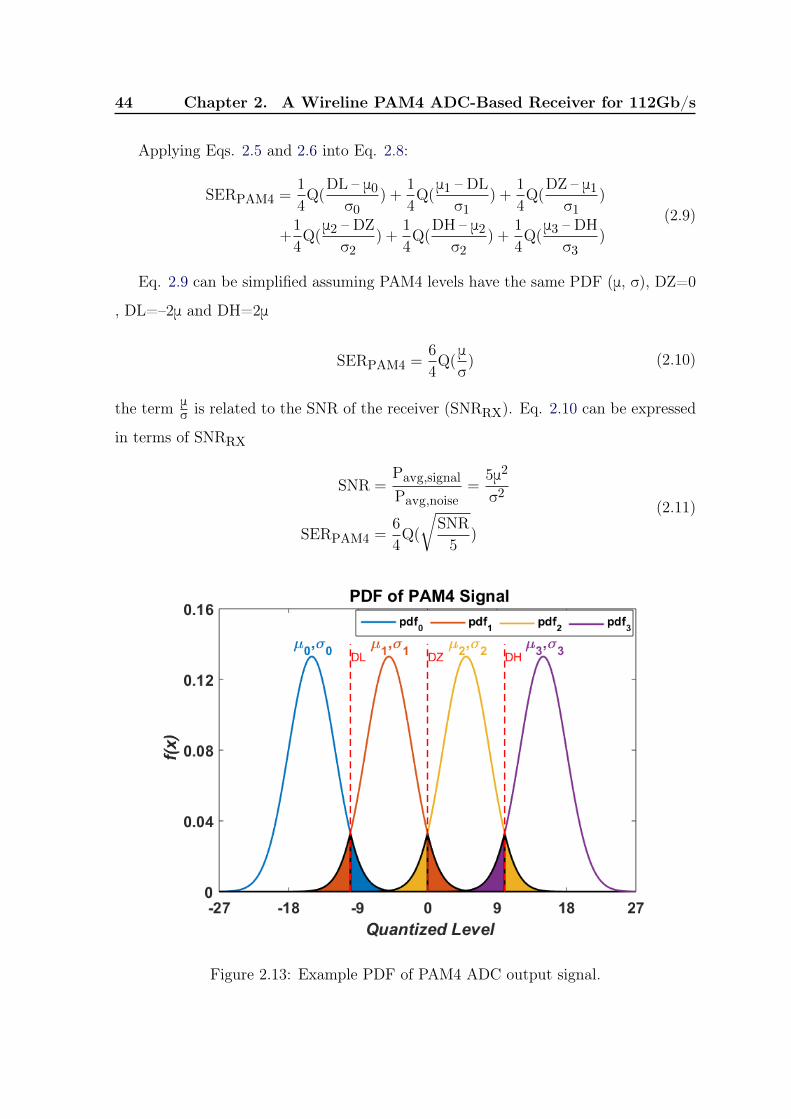
44 Chapter 2. A Wireline PAM4 ADC-Based Receiver for 112Gb/s
Applying Eqs. 2.5 and 2.6 into Eq. 2.8:
SERPAM4 =1
4Q(
DL – μ0σ0
) +1
4Q(μ1 – DL
σ1) +
1
4Q(
DZ – μ1σ1
)
+1
4Q(μ2 – DZ
σ2) +
1
4Q(
DH – μ2σ2
) +1
4Q(μ3 – DH
σ3)
(2.9)
Eq. 2.9 can be simplified assuming PAM4 levels have the same PDF (μ, σ), DZ=0
, DL=–2μ and DH=2μ
SERPAM4 =6
4Q(μ
σ) (2.10)
the term μ
σis related to the SNR of the receiver (SNRRX). Eq. 2.10 can be expressed
in terms of SNRRX
SNR =Pavg,signal
Pavg,noise=
5μ2
σ2
SERPAM4 =6
4Q(
√SNR
5)
(2.11)
Figure 2.13: Example PDF of PAM4 ADC output signal.

2.4. Link System Simulation 45
BER is related to SER, but is also related to the coding scheme. Using Gray coding
only one bit error per symbol is made for incorrect decisions. Thus, BER is half of
SER for PAM4 signaling adopting gray coding.
BERPAM4,gray–coding =SERPAM4
2=
3
4Q(
√SNR
5) (2.12)
This expression is the same as presented in Eq. 1.1, interchanging the function Q(·)for erfc. For simplicity, the system simulations refer only to BER.
2.4.3 Simulation results
Figure 2.14 depicts the simulink model to evaluate the receiver. As described in section
1.2.2, it includes a CDR: a PLL loop extracts the clock signal from the output of the
CTLE and sends it to the ADC and DSP.
The link was tested using 5×10⁵ symbols with a PRQS7 pattern and noise in the
transmitter. De-emphasis was not implemented because the large number of RX FFE
taps is dominant in the equalization. The histograms of the channel, CTLE and ADC
are shown in Figure 2.15. The CTLE performs two functions: giving a gain boosting
at Nyquist and controlling gain to avoid signal clipping. The ADC quantization helps
to restore some of the transmitted signal and also to define the slicers threshold (DL,
DZ, DH) in the DFE. The ADC output is equalized in the digital domain using FFE
and DFE. The equalized histogram is shown in Figure 2.16. FFE taps were calculated
Figure 2.14: High speed serial link simulink model.

46 Chapter 2. A Wireline PAM4 ADC-Based Receiver for 112Gb/s
Figure 2.15: Transmitted symbols: channel, CTLE and ADC.
using 10-bit-wide operations. The output of the receiver is decoded to its correspondent
PAM4 level and compared to the transmitted symbols.
The output of the receiver before decoding is presented in Figure 2.17. It can
be seen that the DFE output levels fall between four distinct groups, Level0,1,2,3,
that represent the PAM4 symbols. Level0,1,2,3 groups are created using the slicer’s
threshold as reference. In order to calculate the BER, each Level0,1,2,3 group is
represented as a RV (μ and σ) with a PDF extracted from the quantized values within
each group. Figure 2.18 shows the PDF for each Level0,1,2,3 with a BER calculated
using Eq. 2.9.
A BER parametrization has been evaluated under two conditions:
1. Fixed CTLE peak gain and FFE weight bit number. For this condition, the
impact of the number of FFE post-taps and DFE was evaluated,

2.4. Link System Simulation 47
Figure 2.16: Symbols after (FFE+DFE) and comparison between TX and RX symbols.
2. Fixed FFE 3pre-/28post-taps and 1 DFE tap. Varying the CTLE peak gain and
the FFE weight bit number.
The parametrization results are shown in Figure 2.19. For the first condition,
DFE has an impact of two orders of magnitude on the BER and it presents linear
decrements for higher number of FFE post-taps. Although FFE is enough to meet the
BER specification range (1×10⁻⁴ to 1×10⁻⁵), the receiver still will use DFE for more
stringent specifications. For the second, a minimum peak gain of 19dB is necessary to
comply with the BER specification range. For the FFE weight bit number, a resolution
higher than 5 bits should be enough to meet the BER.
The feasibility of an ADC-based receiver that meets Long Reach (LR) applications
for 112Gb/s through the selection of a physical backplane channel. A demonstration
is made by performing a link system simulation.

48 Chapter 2. A Wireline PAM4 ADC-Based Receiver for 112Gb/s
Figure 2.17: Sampled equalized symbols at the RX output.
Figure 2.18: PDF of PAM4 RX output signal.

2.4. Link System Simulation 49
Figure 2.19: BER Parametrization: FFE post-taps and CTLE peaking gain.

50 Chapter 2. A Wireline PAM4 ADC-Based Receiver for 112Gb/s
2.5 Conclusion
This chapter has presented a methodology to evaluate receiver’s specifications using
link system analysis. A complete high-speed serial link in MATLAB Simulink was
implemented for simulation. Through link simulation a wireline receiver with the
following characteristics has been validated:
• PAM4 modulation: multi-level signaling is needed to overcome bandwidth
limitation of NRZ modulation,
• ADC-based architecture: mixed-signals were most of the equalization is
implemented in the digital domain will be the norm for speed beyond 100Gb/s,
• CTLE: the AFE of the receiver will require an analog equalizer for gain boosting
and signal conditioning before the ADC,
• FFE + DFE: due to the high channel losses, a combination of long FFE taps
with one-tap DFE presents the best solution to cancel ISI,
• Long Reach applications: the receiver is capable to equalize input data with
channel losses close and up to 30dB,
• Raw BER: through a combination of CTLE, FFE and DFE applied to an
ADC-based architecture, the BER is within the specified range of 1×10⁻⁴ to
1×10×–5.
These characteristics are compatible with the latest CMOS technologies
which will allow a full-integrated solution. Chapter 3 presents the design of the
core of the receiver -the ADC- and the the clock generation circuit.

Chapter 3
7b 56GS/s HierarchicalTime-Interleaved SAR ADC
Contents3.1 Design Flow . . . . . . . . . . . . . . . . . . . . . . . . . . . . . . 52
3.2 Time-Interleaved ADCs . . . . . . . . . . . . . . . . . . . . . . . 52
3.2.1 Fundamentals of Time-Interleaved ADCs . . . . . . . . . . . . . . 52
3.2.2 Signal-to-Noise . . . . . . . . . . . . . . . . . . . . . . . . . . . . 57
3.2.3 ADC resolution estimation . . . . . . . . . . . . . . . . . . . . . 58
3.3 Hierarchical TI-ADC . . . . . . . . . . . . . . . . . . . . . . . . 60
3.3.1 Sampling capacitor estimation . . . . . . . . . . . . . . . . . . . . 60
3.3.2 Direct and Inline Demux Sampling . . . . . . . . . . . . . . . . . 61
3.3.3 3-Rank Hierarchical TI-ADC . . . . . . . . . . . . . . . . . . . . 65
3.4 Clock generation and distribution . . . . . . . . . . . . . . . . . 74
3.5 Sub-ADC implementation . . . . . . . . . . . . . . . . . . . . . 78
3.5.1 Architecture Selection . . . . . . . . . . . . . . . . . . . . . . . . 78
3.5.2 Circuit Description . . . . . . . . . . . . . . . . . . . . . . . . . . 80
3.5.3 Capacitive DAC . . . . . . . . . . . . . . . . . . . . . . . . . . . 82
3.5.4 Comparator . . . . . . . . . . . . . . . . . . . . . . . . . . . . . . 84
3.5.5 SAR Logic . . . . . . . . . . . . . . . . . . . . . . . . . . . . . . 86
3.6 Simulation Results . . . . . . . . . . . . . . . . . . . . . . . . . . 87
3.6.1 Sub-ADC . . . . . . . . . . . . . . . . . . . . . . . . . . . . . . . 87
3.6.2 TI-ADC . . . . . . . . . . . . . . . . . . . . . . . . . . . . . . . . 92
3.7 Conclusion . . . . . . . . . . . . . . . . . . . . . . . . . . . . . . . 97

52 Chapter 3. 7b 56GS/s Hierarchical Time-Interleaved SAR ADC
This chapter presents the design of a 56GSample/s Time-Interleaved ADC for
ADC-based wireline receivers. The first subsection describes the concept of TI-ADCs,
state-of-the-art and same design considerations. The following subsections cover
design, clock generation and simulation results.
3.1 Design Flow
Some guidelines for the design of a high-speed TI-ADC are defined. Figure 3.1 presents
the TI-ADC design flow. It is described as follows:
• A theoretical revision and state-of-the-art trends on TI-ADCs is conducted,
• the design procedure is divided in: hierarchical Track-and-Hold (TH), clock
generation and sub-ADC design,
• the number of TH ranks are chosen to minimize the amount of low-jitter sampling
clocks. Then, the TH stages are designed,
• the sampling clocks are designed accordingly to the hierarchical TH,
• the sub-ADC resolution is calculated based on the system level SNR. Then, the
architecture is chosen to complete the sub-ADC design,
• the TI-ADC is assembled and simulated. Specifications are verified to comply
with the design.
3.2 Time-Interleaved ADCs
3.2.1 Fundamentals of Time-Interleaved ADCs
High-speed data converters aiming for or above 1GS/s often use a Time-Interleaved
(TI) architecture [28] to achieve the highest sample rate. One method to compare the
performance of ADCs is by using a Figure-Of-Merit (FOM), which is applicable on

3.2. Time-Interleaved ADCs 53
TI-ADCDesign
Procedure
Revision:
Theory and State-of-the-art
ClockGeneration
HierarchicalTrack and Hold (TH)
sub-ADC resolutionBased on SNR
SAR ADC Design
# of Ranks:
Minimize
low-jitter clocks
TH Design:Buffer/Gain stages,
SwitchesTI-ADC
Simulation
Finish?
Done
yes
no:Verify:SNDR,Power
Figure 3.1: Time-Interleaved ADC design flow
all converter architectures and is used to show the ongoing trends in ADC designs. A
well-used FOM is the Walden FOM (FOMW), defined as
FOMW =P
2ENOB · FS(3.1)
where FS is the full sampling rate, ENOB is the effective number of bits and P is the
total power consumption of the converter.
Figure 3.2 shows the FOMW versus the Nyquist sampling rate (fs,nyq) for all ADCs
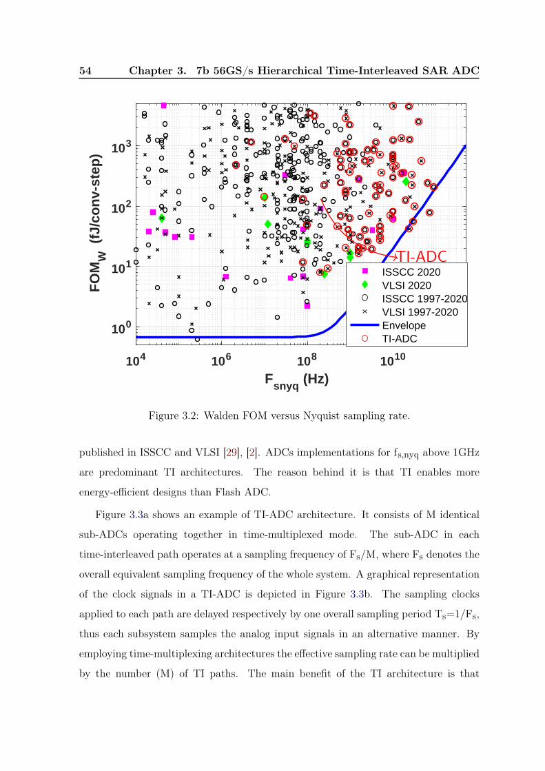
54 Chapter 3. 7b 56GS/s Hierarchical Time-Interleaved SAR ADC
104 106 108 1010
Fsnyq (Hz)
100
101
102
103
FO
MW
(fJ
/co
nv-
step
)
ISSCC 2020VLSI 2020ISSCC 1997-2020VLSI 1997-2020EnvelopeTI-ADC
TI-ADC
Figure 3.2: Walden FOM versus Nyquist sampling rate.
published in ISSCC and VLSI [29], [2]. ADCs implementations for fs,nyq above 1GHz
are predominant TI architectures. The reason behind it is that TI enables more
energy-efficient designs than Flash ADC.
Figure 3.3a shows an example of TI-ADC architecture. It consists of M identical
sub-ADCs operating together in time-multiplexed mode. The sub-ADC in each
time-interleaved path operates at a sampling frequency of Fs/M, where Fs denotes the
overall equivalent sampling frequency of the whole system. A graphical representation
of the clock signals in a TI-ADC is depicted in Figure 3.3b. The sampling clocks
applied to each path are delayed respectively by one overall sampling period Ts=1/Fs,
thus each subsystem samples the analog input signals in an alternative manner. By
employing time-multiplexing architectures the effective sampling rate can be multiplied
by the number (M) of TI paths. The main benefit of the TI architecture is that

3.2. Time-Interleaved ADCs 55
the overall sample-rate can be very high, while the sub-ADCs only need a moderate
sample-rate enabling a high power efficiency.
In principle, the operating speed of the TI-ADC can grow linearly by increasing
the number of parallel ADC channels. However, various types of mismatches among
different channels create modulation tones which degrade the performance of the
TI-ADC, like offset, gain, timing as well as bandwidth mismatches [30],[31]. The
timing-mismatch is the largest problem in high-speed TI-ADCs. All these limitations
occur in the frequency domain as spurious tones and therefore degrade the Spurious
Free Dynamic Range (SFDR) and the Signal-to-Noise-and-Distortion Ratio (SNDR)
of the TI-ADC.
Figure 3.3: A TI-ADC: (a) The overall system architecture. (b) timing diagram.
Table 3.1: Mismatches in TI-ADCs
Mismatches
Offset Gain Timing
Generates spurs
Location dependent Location dependent on numberon number of channels of channels and input frequency
Independent of Power of spurssignal amplitude dependent on signal amplitude
Independent of Power of spurs independent Power of spurs dependentinput frequency of input frequency on input frequency

56 Chapter 3. 7b 56GS/s Hierarchical Time-Interleaved SAR ADC
Figure 3.4: Time-interleaved ADC mismatches example: Offset, gain, timing and allmismatch errors. Fin=27.66GHz 16384 point FFT.
An overview of the spectral signatures of the mismatches in TI-ADCs is given in
Table 3.1. A simulation of the TI-ADC (coherent sampling of a sine wave at Nyquist
frequency) was performed with sampling rate Fs=56GS/s, M=64, 7-bit resolution and
sampling jitter, σjitter=0.1%Ts. Offset, gain and timing mismatch were modeled as a
random numbers within a pre-defined range.
The output spectrum for each individual error and combined mismatch errors is
shown in Figure 3.4. Timing mismatch is the dominant error source. For this reason,
special care must be taken in the clock routing and distribution.

3.2. Time-Interleaved ADCs 57
3.2.2 Signal-to-Noise
As the ADC rounds the signal to the closest level, a triangular shaped error signal
will arise. This saw-tooth signal is the fundamental quantization error and varies
linearly from +0.5ALSB and -0.5ALSB. The PDF is assumed constant and uniformly
distributed. The quantization error power (PQ) is determined by calculating the
estimation value for the variance and yields:
PQ =A2LSB
12=
(full – scale
2N√12
)2
(3.2)
where ALSB refers to the size of the least significant bit, “full-scale” is the analog range
of the conversion and N the resolution.
Often in analog-to-digital converters sinusoidal signals are used to characterize
the performance. The quantization error is related to the maximum sinusoidal signal
(Asin(ωt)) that the analog-to-digital converter can handle [32]. The quantization errors
of the analog-to-digital converter are considered uncorrelated. The resulting noisy
spectrum is modeled as a white noise spectrum, whose power is contained between
f=0 and f=fs/2 and mirrored around the multiples of the sample rate.
The SNR compares the noise power in a full sine wave as
SNR = 10 · log10(
Psignal
Noise power
)(3.3)
PQ can be used to calculate an equivalent SNR
Psignal =1
T
∫ t=T
t=0A2sin2(ωt) dt =
A2
2=
22NA2LSB
8
SNRmag =Psignal
PQ=
3
222N
SNRdB = 10 · log10(3
222N)
= 1.76 + N× 6.02dB
(3.4)
Eq. 3.4 is an approximation that is often used in ADC design. It defines the
maximum SNR represented by a digital word of N bits in a bandwidth of fs/2.
The SNDR stands for the ratio of the signal power to all the unwanted components:
quantization errors, thermal noise, distortion, timing mismatch[31].
SNDR = 10 · log10(
Power of 1st harmonic
Power of all unwanted components
)(3.5)

58 Chapter 3. 7b 56GS/s Hierarchical Time-Interleaved SAR ADC
The SFDR is the distance between the signal and the largest single unwanted
component, the spurious signal. In order to characterize the converter in a simple
manner, the Effective Number Of Bits (ENOB) is calculated by reversing Eq. 3.4:
ENOB =SNDR – 1.76
6.02(3.6)
The ENOB allows an easy comparison of the real performance of an ADC. Another
well-used FOM is the Schreier FOM (FOMS)
FOMS = SNDR+ 10 · log10(BW
P) (3.7)
which uses the SNDR, signal bandwidth (BW) and the total power consumption P.
3.2.3 ADC resolution estimation
Figure 3.5: sub-ADC in a TI System.
In the previous chapter, the ADC used in the system simulation had a pre-defined
resolution of 7 bits. The resolution of the TI-ADC will be calculated using the BER at
the output of the receiver (pre-FEC or raw BER). Figure 3.5 depicts the link budget
for an ADC-based receiver. In contrast to the model in chapter 2, the gain at Nyquist
3.2. Time-Interleaved ADCs 59
frequency have been distributed between TX and RX, which corresponds to a more
realistic implementation.
The TI-ADC is designed to meet the SNR requirements for 56GBaud PAM4
signaling. Forward Error Correction (FEC) will be used to improve link integrity and
counteract physical layer level errors introduced by reduced SNR in PAM4 signaling
[33].
In the previous chapter, a target pre-FEC BER range of [1×10⁻⁴ - 1×10⁻⁵] wasused. For this scenario, a BER=1 × 10⁻⁶ (adding additional margin) over 30dB loss
channel was employed. We start calculating the output SNR, which corresponds to a
post-FEC BER=1× 10–15, using Eq. 1.11, [7]:
BERpost,FEC = 1× 10–15 =
(3
8
)× erfc
(√SNR
10
)
SNR ≈ 25dB
(3.8)
For a FEC gain of 3.8dB, the pre-FEC BER is
25dB︸ ︷︷ ︸BERpost,FEC
– 3.8dB︸ ︷︷ ︸GainFEC
= 21.2dB︸ ︷︷ ︸BERpre,FEC<1×10⁻⁶
(3.9)
The DSP equalization boost is calculated as
30dB︸ ︷︷ ︸channel loss
– 8dB︸︷︷︸Txgain
– 8dB︸︷︷︸ = 14dB
Rxgain
(3.10)
Considering a SNR noise penalty of -0.5dB per dB of DSP boost and a margin of 6dB,
the SNR requirement at the input of the ADC yields:
SNRADC = 21.2dB︸ ︷︷ ︸BERpre,FEC<1×10⁻⁶
+ 14× 0.5 dB︸ ︷︷ ︸No,DSP
+ 6dB︸︷︷︸Margin
= 34.2dB (3.11)
Using Eq. 3.6, the ADC resolution yields to ≈ 5.4 bits. This is the minimum
resolution required to meet the target BER. Our design targets a resolution of 7 bits
as a trade-off of speed and power for a single-channel ADC.
1Eq. 2.11 can be used as well
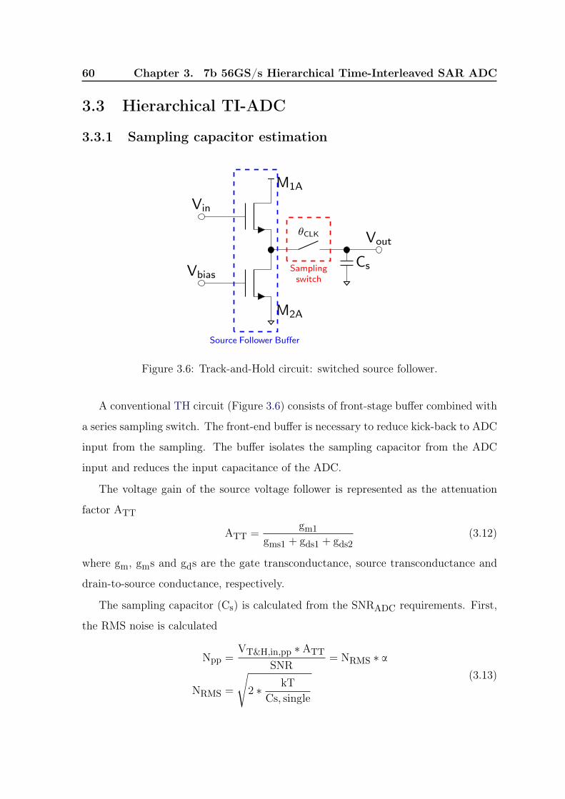
60 Chapter 3. 7b 56GS/s Hierarchical Time-Interleaved SAR ADC
3.3 Hierarchical TI-ADC
3.3.1 Sampling capacitor estimation
M1A
Vin
θCLK
Cs
Vout
M2A
Vbias
Source Follower Buffer
Samplingswitch
Figure 3.6: Track-and-Hold circuit: switched source follower.
A conventional TH circuit (Figure 3.6) consists of front-stage buffer combined with
a series sampling switch. The front-end buffer is necessary to reduce kick-back to ADC
input from the sampling. The buffer isolates the sampling capacitor from the ADC
input and reduces the input capacitance of the ADC.
The voltage gain of the source voltage follower is represented as the attenuation
factor ATT
ATT =gm1
gms1 + gds1 + gds2(3.12)
where gm, gms and gds are the gate transconductance, source transconductance and
drain-to-source conductance, respectively.
The sampling capacitor (Cs) is calculated from the SNRADC requirements. First,
the RMS noise is calculated
Npp =VT&H,in,pp ∗ ATT
SNR= NRMS ∗ α
NRMS =
√2 ∗ kT
Cs, single
(3.13)

3.3. Hierarchical TI-ADC 61
Figure 3.7: State-space design for the sampling capacitor (Cs).
where α=9.507 with a BER=1× 10⁻⁶. The design of the sampling capacitor is shown
in Figure 3.7 for an input of 400mVpp. Different values of ATT, representing Process
Voltage Temperature (PVT) variations, for the source voltage follower are considered.
A sampling capacitor of 19.54fF with an ATT=1.5dB2 yields an equivalent resolution
of 5.4 bits.
3.3.2 Direct and Inline Demux Sampling
Voltage-based TH can be categorized in direct and inline demux sampling [34], [35],
[36], [37]. Both designs implement subsampling to achieve a higher Interleaved
Sampling Ratio (ISR).
1. Direct sampling, shown in Figure 3.8(a), provides the shortest path from
the input to the sampling capacitor with minimum resistance. N1 denotes
interleaving ratio as well as the total amount of sampling switches. One or more
2Represents a typical Source Follower Voltage Gain of 0.85 in 22nm CMOS FDSOI

62 Chapter 3. 7b 56GS/s Hierarchical Time-Interleaved SAR ADC
Vin
Sampling
switches
1 : N1 interleavingN1,c switches on
Direct Sampling(a)
. . .
. . .
. . .
. . .
ϕ1
Cs,1
ϕ2
Cs,1
ϕ3
Cs,1
ϕ4
Cs,1
Vin
Sampling
switches
1 : N1 interleavingN1,c switches on
1 : N2 interleaving1 switches on
Inline Demux Sampling(b)
Inline Demuxswitches
ϕ1
ϕ2
. . .
ϕ3
ϕ4
. . .
Θ11
. . .Cs,1
Θ12
. . .Cs,1
Θ13
. . .Cs,1
Θ14
. . .Cs,1
Θ31
. . .Cs,1
Θ32
. . .Cs,1
Θ13
. . .Cs,1
Θ14
. . .Cs,1
Figure 3.8: (a) Direct sampling. (b) Inline demux sampling.
of the sampling switches are closed at the same time, N1,c. If only one switch is
closed at a time, the bandwidth is the largest but the shortest sampling pulses
are required. Direct sampling is very efficient for a small number of parallel
switches (usually ≤ 8), as too many switches will increase the input capacitance
at the input node. The sampled voltage is stored on the sampling capacitor Cs.
2. Inline demux sampling, shown in Figure 3.8(b), stacks two switches to reduce
the number of parallel switches at the input. N2 represents the total number of
inline demux switches and N1 × N2 is the interleaving ratio. The inline demux
switch closes before the sampling switch closes and opens after the sampling
switch opens. Thus, the sampling time depends only on the falling edge of the

3.3. Hierarchical TI-ADC 63
sampling switch clock. The use of inline demux switches significantly reduces
the number of timing critical clock signals.
At first glance, inline demux sampling allows higher ISR than direct sampling. To
gain more insight into the advantage of one method over the other, an interleaver
bandwidth analysis for the two methods was implemented. A simplified model for a
cross-coupled switch is applied, as shown in Figure 3.9a. Ron, Cin and Cout correspond
to a single switch transistor. A correction factor p is used to take into account the
parasitic capacitors and resistors. The sampling capacitor is determined by the kT/C
noise for the target SNDR.
Figure 3.9a, b present the RC model for the interleavers depicted in Figure 3.8.
The elements of the RC circuit can be expressed by the interleaver parameters N1,
N1,c, N2, the switch parameters Ron, Cin and Cout, the total sampling capacitor Cs
vs
θCLK
Cin
Ron
Cout
k = |gds
VDS=0V
gmVDS=VDD/2
|VGS=VDD−VIN
Cin = Csb + Cgs ≈ Cgg/2
Cout = Cdb + Cgd ≈ Cgg/2
Ron =1gds
= 1k·gm
⇒
(a)
vsReq
Ceq
ωeq = ωout · p = 1RonCout
· p
Vin
Rin
C1
R2
C2
Vdirect
(b)
Vin
Rin
C0
R1
C1
R2
C2
Vdemux
(c)
Cout
θCLK
VBBN
(WnL
)
RonVIN+
Cout′
GND
VBBN
(WnL
)
VIN−
Cs
Crosscoupledswitchdetail
Figure 3.9: (a) Switch model and detail of parasitics. (b) RC model for Directsampling. (c) RC model for Inline demux sampling.
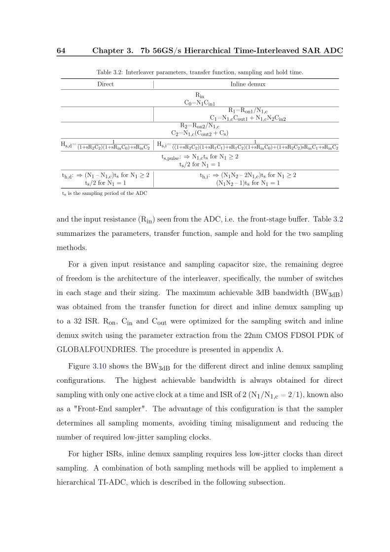
64 Chapter 3. 7b 56GS/s Hierarchical Time-Interleaved SAR ADC
Table 3.2: Interleaver parameters, transfer function, sampling and hold time.
Direct Inline demux
RinC0=N1Cin1
R1=Ron1/N1,cC1=N1,cCout1 +N1,cN2Cin2
R2=Ron2/N1,cC2=N1,c(Cout2 + Cs)
Hs,d= 1(1+sR2C2)(1+sRinC0)+sRinC2
Hs,i= 1((1+sR2C2)(1+sR1C1)+sR1C2)(1+sRinC0)+(1+sR2C2)sRinC1+sRinC2
ts,pulse: ⇒ N1,cts for N1 ≥ 2ts/2 for N1 = 1
th,d: ⇒ (N1 – N1,c)ts for N1 ≥ 2 th,i: ⇒ (N1N2 – 2N1,c)ts for N1 ≥ 2ts/2 for N1 = 1 (N1N2 – 1)ts for N1 = 1
ts is the sampling period of the ADC
and the input resistance (Rin) seen from the ADC, i.e. the front-stage buffer. Table 3.2
summarizes the parameters, transfer function, sample and hold for the two sampling
methods.
For a given input resistance and sampling capacitor size, the remaining degree
of freedom is the architecture of the interleaver, specifically, the number of switches
in each stage and their sizing. The maximum achievable 3dB bandwidth (BW3dB)
was obtained from the transfer function for direct and inline demux sampling up
to a 32 ISR. Ron, Cin and Cout were optimized for the sampling switch and inline
demux switch using the parameter extraction from the 22nm CMOS FDSOI PDK of
GLOBALFOUNDRIES. The procedure is presented in appendix A.
Figure 3.10 shows the BW3dB for the different direct and inline demux sampling
configurations. The highest achievable bandwidth is always obtained for direct
sampling with only one active clock at a time and ISR of 2 (N1/N1,c = 2/1), known also
as a "Front-End sampler". The advantage of this configuration is that the sampler
determines all sampling moments, avoiding timing misalignment and reducing the
number of required low-jitter sampling clocks.
For higher ISRs, inline demux sampling requires less low-jitter clocks than direct
sampling. A combination of both sampling methods will be applied to implement a
hierarchical TI-ADC, which is described in the following subsection.

3.3. Hierarchical TI-ADC 65
Figure 3.10: Maximum achievable 3dB bandwidth (BW3dB) versus hold time fordifferent direct sampling and inline demux sampling configurations. L = 20nm,VS,D =0.35V, VG = 0.8V, VB = 1.8V and Cs = 20fF
3.3.3 3-Rank Hierarchical TI-ADC
In order to reduce the number of required low-jitter clocks for sampling and to avoid
complicated delay calibration of multiple clock phases, a hierarchical architecture is
chosen for the TH circuit [36]. Figure 3.11 shows the architecture. It implements an
ISR of 64 distributed into three ranks of TH:
1. First rank is a 2-way TI TH stage at half rate (28GHz),
2. Second rank is a 8-way TI TH stage at 3.5GHz,
3. Third rank is a 4-way TI TH stage at 875MHz.
This architecture gives us the best trade-off in terms of bandwidth and number of
low-jitters clocks. By using the first rank as front-end sampler at half rate, it only
requires two low-jitter clocks at 28GHz or one differential. For the second and third

66 Chapter 3. 7b 56GS/s Hierarchical Time-Interleaved SAR ADC
BF1Vin
θ28G
θ28G
Cs1
Cs1
BF2
BF2
θ3.5G,[0]
Cs2
θ3.5G,[2]
Cs2
θ3.5G,[4]
Cs2
θ3.5G,[6]
Cs2
θ3.5G,[8]
Cs2
θ3.5G,[10]
Cs2
θ3.5G,[12]
Cs2
θ3.5G,[14]
Cs2
...
. . .
...
. . .
...
. . .
...
. . .
...
. . .
...
. . .
...
. . .
θ3.5G,[1]
Cs2
θ3.5G,[3]
Cs2
θ3.5G,[5]
Cs2
θ3.5G,[7]
Cs2
θ3.5G,[9]
Cs2
θ3.5G,[11]
Cs2
θ3.5G,[13]
Cs2
θ3.5G,[15]
Cs2
...
. . .
...
. . .
...
. . .
...
. . .
...
. . .
...
. . .
...
. . .
...
. . .
BF3
θ875M,[0]AD
θ875M,[16]AD
θ875M,[32]AD
θ875M,[48]AD1 : 2
Rank− 1
1 : 8
Rank− 2
1 : 4
Rank− 3
T28G︸︷︷︸35.71ps
[email protected]% = 285.71ps
T875M@25% = 1.14ns
28GHz [0]
3.5 GHz [0]
875MHz [0]
Figure 3.11: Architecture of the 3-rank hierarchical TI-ADC
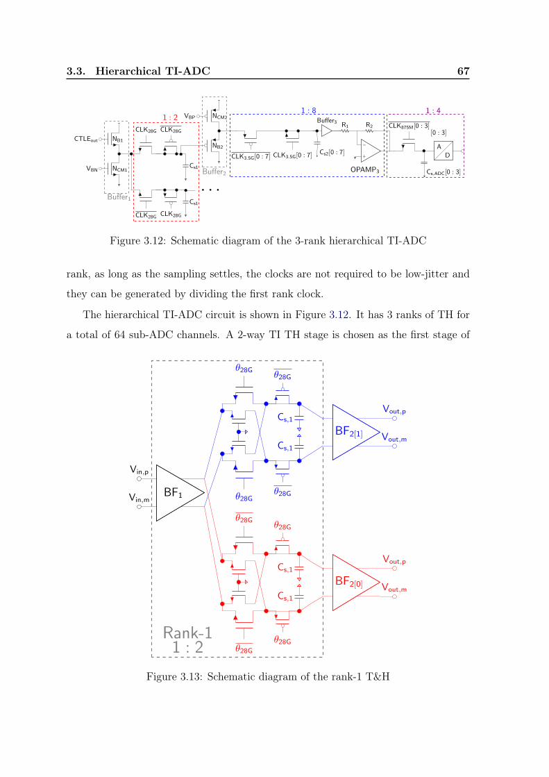
3.3. Hierarchical TI-ADC 67
CTLEout NB1
VBN NCM1
CLK28G CLK28G
Cs1
CLK28G CLK28G
Cs1
· · ·
1 : 2
NB2
VBP NCM2
Buffer1
Buffer2
CLK3.5G[0 : 7]Cs2[0 : 7]CLK3.5G[0 : 7]
1 : 8Buffer3
−
+
R1 R2
OPAMP3
CLK875M[0 : 3]
Cs,ADC[0 : 3]
AD
[0 : 3]
1 : 4
Figure 3.12: Schematic diagram of the 3-rank hierarchical TI-ADC
rank, as long as the sampling settles, the clocks are not required to be low-jitter and
they can be generated by dividing the first rank clock.
The hierarchical TI-ADC circuit is shown in Figure 3.12. It has 3 ranks of TH for
a total of 64 sub-ADC channels. A 2-way TI TH stage is chosen as the first stage of
Vin,p
Vin,mBF1
θ28Gθ28G
Cs,1
Vout,p
Vout,mBF2[1]
θ28Gθ28G
Cs,1
θ28Gθ28G
Cs,1
Vout,p
Vout,mBF2[0]
θ28Gθ28G
Cs,1
Rank-11 : 2
Figure 3.13: Schematic diagram of the rank-1 T&H

68 Chapter 3. 7b 56GS/s Hierarchical Time-Interleaved SAR ADC
Figure 3.14: Signals of the rank-1 T&H
the hierarchical TH. A source voltage follower with cross-coupled switches shows the
best trade-off between voltage headroom and linearity. As described before, rank-1
is 2-way TI TH circuit sampled at 28GHz. A passive gain is implemented using the
PMOS dummy switch varying its capacitance from track to hold operation [38]. This
technique allows to passively amplify the sampled signal and thus to improve the SNR.
The total sampling capacitance Cs1 consists of the parasitics of the switches and
the input capacitance of the voltage follower of rank-2. Figure 3.14 shows the track
and hold operation in rank-1. The input signal is sampled at 28GHz with a sample
transition in the middle of the tracking interval. The passive gain at the output of
the switch is shown during the hold interval. It will improve the SNR in the following
rank. The buffers used in rank-1 are source voltage followers, as shown in Figure 3.15a.
Rank-2 is an 8-way TI TH circuit sampled at 3.5GHz. The buffer used in
this stage (Buffer2) is a gain-boosted Flipped Voltage Follower (FVF) (as seen in
Figure 3.15) [39]. The Flipped Voltage Follower (FVF) technique delivers a smaller
output resistance compared to a conventional source follower. Thus, allowing a higher
bandwidth for the same power consumption. The gain is achieved by cross-coupling

3.3. Hierarchical TI-ADC 69
the NMOS transistors (M4A–4B) to form a pseudo-differential common source stage.
A back gate biasing control is implemented for PVT variations. The bandwidth is
extended by introducing a feedback capacitor C [40]. The DC bias of the top PMOS
transistors (M3A–3B) is set by VBP through large bias resistors.
Figure 3.12 shows the eight PMOS cross-coupled switches sampled by eight
non-overlapping clock signals. To improve the isolation between rank-2 and rank-3,
the output of each switch is passed through a buffer (Buffer3). These buffers are scaled
versions of the buffer in rank-1. The duty-cycle of the sampling clocks for rank-2 and
rank-3 are set so that only 1 interleaved switch following the inter-rank buffer is closed
at any given time.
Figure 3.16 shows the time diagram for the TH operation in rank-2. It starts with
tracking the Buffer2 output. Buffer3 reads the output of the PMOS switches (Switch2)
and transfers it to the input of the gain stage (OpAmp3) of rank-3.
The rank-3 is a 4-way TI TH circuit sampled at 875MHz. Figure 3.12 shows 4
NMOS switches, representing the TH stage of a sub-ADC unit. Each 4-way TI TH
VBB1
M1A
Vin,p
Vout,p
VBB2
M2A
VBN
(a)
VBB1
M1B
Vin,m
Vout,m
VBB2
M2B
VBN
M1AVin,p
R
M3A
Vout,p C
RB
M4A
VBB1
M1B Vin,m
R
M3B
Vout,mC
RB
VBP
M4B
VBB1
(b)
Figure 3.15: (a) Rank-1 buffer: Source Follower. (b) Rank-2 buffer: Gain-boostedFlipped Voltage Follower (FVF)

70 Chapter 3. 7b 56GS/s Hierarchical Time-Interleaved SAR ADC
Figure 3.16: Signals of the rank-2 T&H
path is driven by a gain stage.
In order to provide a full-scale input and the correct common mode, as required
by the ADC, a voltage gain stage is implemented using an OpAmp with feedback
resistors (as seen in Figure 3.17a). Since the input common mode coming from Buffer3
is not adequate for the input stage of the OpAmp, an input Common Mode Feedback
(CMFB) is used to fix it to a more suitable value (≈ 250mV). The combined gain
of the rank-1 and rank-2 is lower than 1 (≈ 0.87). Thus, a voltage gain of ≈2.3 is
needed to bring the signal to the full scale level of the ADC. A programmable gain
with +/-25% variation was implemented by adjusting the feedback resistor RFB.
The schematic of the OpAmp is presented in Figure 3.17b. It consists of a
low-voltage fully differential 2-stage amplifier with Miller compensation. It implements
an output common mode feedback circuit to bring the DC output level to VDD/2.
Gain boosting is added to the first stage and can be digitally turned on or off.
Calibration circuits for offset and output common mode are implemented using back

3.3. Hierarchical TI-ADC 71
−
+−+
Vout,p
RFB
RFF
Vin,m
Vout,m
RFB
RFF
Vin,p
Rcm,out
−
+
Rcm,out/2
Vref,out
VOCMFBRcm,in
−
+
Rcm,in/2
Vref,in
VICMFB
(a)
Ib
VG+
VG−
I − CMFB O − CMFB
M1AinpM1B
inm
VBP M5
MCCA
VBB1VBB1
VOCMFBM2A
MCCB
VBB1VBB1
VOCMFBM2B
VBB1CCen
MCCEN
M6A
outp
VBBP
CcRZ
VBPM7A
(b)M6B
outm
VBBP
CcRZ
VBP M7B
Figure 3.17: (a) Diagram of the rank-3 gain stage. (b) Fully differential two-stageOpAmp with gain enhancement.
Figure 3.18: Signals of the rank-3 T&H

72 Chapter 3. 7b 56GS/s Hierarchical Time-Interleaved SAR ADC
gate biasing. The output of the OpAmp needs to settle within the track time of the
ADC (ttrack,ADC=285.76ps). This requirement sets the bandwidth for the OpAmp.
Figure 3.18 shows the TH operation in rank-3. The output of the gain stage
(OpAmp3) is tracked by the ADC (Switch3). The tracked voltage settles within the
ttrack,ADC time.
In Figure 3.19 the non-linearity introduced by the buffers and gain stage is analyzed.
The circuits have been designed to meet an overall variation of 1% for the entire
hierarchical TH.
The BW3dB and power consumption of the hierarchical TH at nominal, slow and
fast corners are presented in Table 3.3. The nominal power consumption is 113.5mW,
where 70% corresponds to rank-3. The rank-1 TH was designed for maximum BW3dB.
Figure 3.20 depicts the voltage gain in the hierarchical TH. A total voltage gain of ≈2 brings the input signal to the full scale of the ADC.
Figure 3.19: Normalized output variation between stages

3.3. Hierarchical TI-ADC 73
Table 3.3: BW3dB and Power Consumption of the Hierarchical TH
Circuit Bandwidth IComp Supply Power(GHz) (mA) (V) (mW)
Buffer1/Switch1 73.21 59.2 46.92 22.31 22.4 22.72 0.8 17.81 17.9 18.22
Buffer2 x2 30.21 25.7 21.32 8.21 7.5 7.22 1 16.41 15 14.42
Switch2 27.21 22.3 17.62
Buffer3 x16 25.61 21.3 16.92 2.441 2.5 2.562 0.8 31.21 32 32.82
OpAmp33 x16 9.41 7.7 5.62 3.761 3.8 3.92 0.8 48.21 48.6 49.92
SwitchADC 8.61 6.4 3.82
Total 113.61 113.5 115.32
1Fast Corner at -40C, 2Slow Corner at 110C, 3At nominal gain
BF1 SW1 BF2 SW2 BF3 VG3 SWADC
Rank circuit
0.5
1
1.5
2
2.5
3
Gai
n (
V/V
)
Hierarchical TH gain
(0.826)
(1.158) (1.100) (1.120)
(0.760)
(2.320)
(0.996)(0.821)
(1.140) (1.120) (1.090)
(0.759)
(2.320)
(0.990)
(0.826)
(1.119) (1.070) (1.073)
(0.755)
(2.310)
(0.992)
(2.07)(1.99)(1.84)
NOMINALSLOW
@110°CFAST
@-40°C
CORNER
Figure 3.20: Hierarchical TH gain for nominal, slow and fast corners
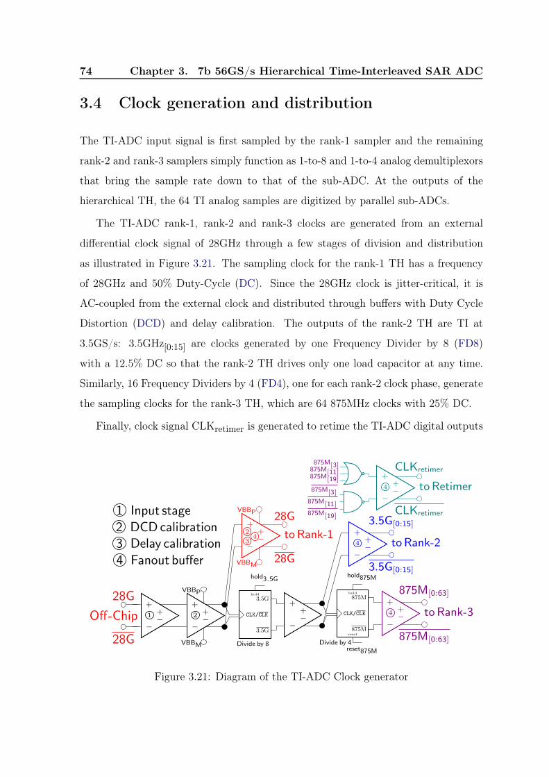
74 Chapter 3. 7b 56GS/s Hierarchical Time-Interleaved SAR ADC
3.4 Clock generation and distribution
The TI-ADC input signal is first sampled by the rank-1 sampler and the remaining
rank-2 and rank-3 samplers simply function as 1-to-8 and 1-to-4 analog demultiplexors
that bring the sample rate down to that of the sub-ADC. At the outputs of the
hierarchical TH, the 64 TI analog samples are digitized by parallel sub-ADCs.
The TI-ADC rank-1, rank-2 and rank-3 clocks are generated from an external
differential clock signal of 28GHz through a few stages of division and distribution
as illustrated in Figure 3.21. The sampling clock for the rank-1 TH has a frequency
of 28GHz and 50% Duty-Cycle (DC). Since the 28GHz clock is jitter-critical, it is
AC-coupled from the external clock and distributed through buffers with Duty Cycle
Distortion (DCD) and delay calibration. The outputs of the rank-2 TH are TI at
3.5GS/s: 3.5GHz[0:15] are clocks generated by one Frequency Divider by 8 (FD8)
with a 12.5% DC so that the rank-2 TH drives only one load capacitor at any time.
Similarly, 16 Frequency Dividers by 4 (FD4), one for each rank-2 clock phase, generate
the sampling clocks for the rank-3 TH, which are 64 875MHz clocks with 25% DC.
Finally, clock signal CLKretimer is generated to retime the TI-ADC digital outputs
1
28G
28G
Off-Chip 2
VBBP
VBBM
3.5G
CLK/CLK
3.5Ghold
Divide by 8
hold3.5G
VBBP
VBBM
2
34
28G
28G
toRank-1
875M
CLK/CLK
875Mhold
reset
hold875M
reset875M
Divide by 4
4
875M[0:63]
875M[0:63]
to Rank-3
4
3.5G[0:15]
3.5G[0:15]
to Rank-2
4
CLKretimer
CLKretimer
to Retimer
875M[3]875M[11]875M[19]
875M[3]
875M[11]
875M[19]1 Input stage2 DCD calibration3 Delay calibration4 Fanout buffer
+
−
+−
+
−
+−
+
−
+−
+
−
+−
+
−
+−
+
−
+−
+
−
+−
Figure 3.21: Diagram of the TI-ADC Clock generator

3.4. Clock generation and distribution 75
before sending them to the DSP unit. It is a 50% DC version of the 875M[3] phase.
This clock is also used by DSP.
The schematic of input stage is presented in Figure 3.22a. It has a 50Ω-input
matching network followed by a high-speed buffer. The latter consists of an
AC-coupling capacitor in series with a resistive feedback inverter for DCD suppression
[41]. The buffer high-pass cutoff frequency can be relatively high (1/10 of the input
frequency) allowing the use of a small Metal-Oxide-Metal (MOM) capacitor. A fan-out
buffer and Transmission Gate (TG) with reset for clock alignment complete the input
stage.
12x 16x 24x
RFBCdecap
50Ω
Vin,m
RFBCdecap
50Ω
Vin,p
32x
CLK/CLK
D Q
D Q
CLK/CLK
D Q
D Q rst
rst
hold28G
rst
rst
rst
Vout,p
Vout,m
+
−
+−
+
−
+−
+
−
+−
+
−
+−
+
−
+
−
(a)
16x
VB
BP
1.6
VV
BB
M1.6
V
C
DE
L[0]
C
DE
L[0]
16x
VB
BP
1.6
VV
BB
M1.6
V
C
DE
L[1]
C
DE
L[1]
16x
VB
BP
CL
KV
BB
PC
LK
C
DE
L[2]
C
DE
L[2]
RFB
RFB
Cdecap
Vin,p
Cdecap
Vin,m
24x
VB
BM
CL
KV
BB
MC
LK
40x
VB
BP
CL
KV
BB
PC
LK
64x
VB
BM
CL
KV
BB
MC
LK
Vout,p
Vout,m
30kΩCAL28G
30kΩ
CAL28G
(b)
+
−
+−
+
−
+−
+
−
+−
+
−
+−
+
−
+−
+
−
+−
Figure 3.22: (a) Input stage. (b) Buffer with DCD and delay calibration.
The schematic of the clock buffer going to rank-1 is shown in Figure 3.22b. It
consists of a high-speed buffer with DCD suppression in series with fan-out buffers.
The resistive feedback inverter chain adds capacitive loads to implement a variable
delay. A 3-bit control gives a total delay variation of 30%UI. The fan-out buffers have
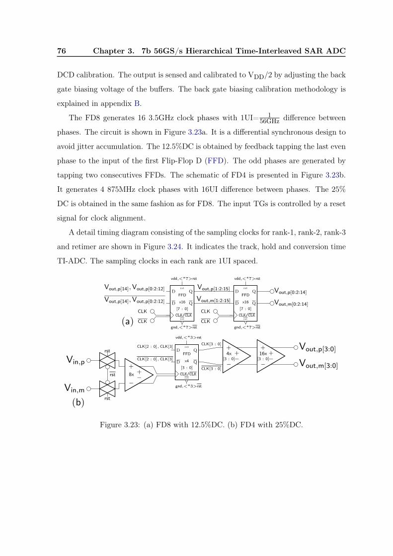
76 Chapter 3. 7b 56GS/s Hierarchical Time-Interleaved SAR ADC
DCD calibration. The output is sensed and calibrated to VDD/2 by adjusting the back
gate biasing voltage of the buffers. The back gate biasing calibration methodology is
explained in appendix B.
The FD8 generates 16 3.5GHz clock phases with 1UI= 156GHz difference between
phases. The circuit is shown in Figure 3.23a. It is a differential synchronous design to
avoid jitter accumulation. The 12.5%DC is obtained by feedback tapping the last even
phase to the input of the first Flip-Flop D (FFD). The odd phases are generated by
tapping two consecutives FFDs. The schematic of FD4 is presented in Figure 3.23b.
It generates 4 875MHz clock phases with 16UI difference between phases. The 25%
DC is obtained in the same fashion as for FD8. The input TGs is controlled by a reset
signal for clock alignment.
A detail timing diagram consisting of the sampling clocks for rank-1, rank-2, rank-3
and retimer are shown in Figure 3.24. It indicates the track, hold and conversion time
TI-ADC. The sampling clocks in each rank are 1UI spaced.
Vin,p
Vin,m
8x
rst
rst
rst CLK/CLK
D Q
D Qrst
rst
FFD
x4
[3 : 0]
vdd,<*3>rst
gnd,<*3>rst
CLK[2 : 0], CLK[3]
CLK[2 : 0], CLK[3]
CLK[3 : 0]
CLK[3 : 0]
4x[3 : 0]
16x[3 : 0]
Vout,p[3:0]
Vout,m[3:0]
(b)
+
−
+−
+
−
+−
+
−
+−
CLK/CLK
D Q
D Qrst
rst
CLK/CLK
D Q
D Qrst
rst
FFD
x16
[7 : 0]
FFD
x16
[7 : 0]
vdd,<*7>rst
gnd,<*7>rst
vdd,<*7>rst
gnd,<*7>rst
Vout,p[14],Vout,p[0:2:12]
Vout,p[14],Vout,p[0:2:12]
Vout,p[1:2:15]
Vout,m[1:2:15]
Vout,p[0:2:14]
Vout,m[0:2:14]
CLK
CLK
CLK
CLK(a)
Figure 3.23: (a) FD8 with 12.5%DC. (b) FD4 with 25%DC.
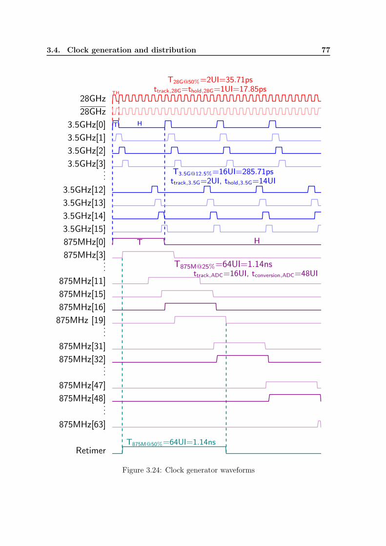
3.4. Clock generation and distribution 77
THttrack,28G=thold,28G=1UI=17.85ps
T28G@50%=2UI=35.71ps
T H
ttrack,3.5G=2UI, thold,[email protected]%=16UI=285.71ps
T875M@25%=64UI=1.14nsttrack,ADC=16UI, tconversion,ADC=48UI
T H
T875M@50%=64UI=1.14ns
28GHz
28GHz
3.5GHz[0]
3.5GHz[1]
3.5GHz[2]
3.5GHz[3]...
3.5GHz[12]
3.5GHz[13]
3.5GHz[14]
3.5GHz[15]
875MHz[0]
875MHz[3]...
875MHz[11]
875MHz[15]
875MHz[16]
875MHz [19]...
875MHz[31]
875MHz[32]...
875MHz[47]
875MHz[48]...
875MHz[63]
Retimer
Figure 3.24: Clock generator waveforms

78 Chapter 3. 7b 56GS/s Hierarchical Time-Interleaved SAR ADC
3.5 Sub-ADC implementation
TI-ADC is implemented using identical sub-ADCs multiplexed in time, operating in
parallel to achieve a higher sampling rate, [34]. Power consumption must be optimized
in the interleaved system.
3.5.1 Architecture Selection
A suitable sub-ADC architecture should not magnify the complexity and the achievable
speed and resolution. The architecture selection was chosen from the energy efficiency
comparison of two high-speed, medium-resolution converters: the flash ADC and SAR
ADC.
An N-bit flash ADC is composed of 2N-1 comparators, a reference resistor ladder
and a thermometer-to-binary encoder as shown in Figure 3.25(a). The reference
resistor ladder and thermometer-to-binary encoder energies scale roughly as 2N but are
usually less than the total comparator energy. For simplicity, the speed and structure of
the comparators used in Flash and SAR ADC are assumed to be the same. Therefore,
the energy per conversion for a flash ADC is
Ecomp = ClatchV2DD
Eflash = (2N – 1) · Ecomp,(3.14)
where Ecomp is the energy of a single comparator. Clatch and VDD represent the total
R
R
R
R
R
VREF
(a)
−
+
−
+
...−
+
VIN
Thermometer
to
Binary
Nbits
Φs
2N−1Cu 4Cu 2Cu Cu Cu
(b)
VIN
VREF
Binary Cap.DAC
−
+SAR
Logic
NbitsVX
Figure 3.25: (a) Flash ADC. (b) SAR ADC with binary-weighted capacitive DAC.

3.5. Sub-ADC implementation 79
switched capacitance in the comparator’s latch and supply voltage, respectively.
A basic SAR ADC structure is shown in Figure 3.25(b). It consists of a comparator,
a capacitive DAC and a SAR control logic. There are several switching schemes aiming
to improve the energy efficiency in SAR ADCs [42]. For simplicity, the conventional
switching scheme is used in this comparison. The energy per conversion of the
comparator can be calculated similar to a flash ADC.
The capacitive DAC using the conventional switching scheme presents a total array
energy for one conversion is
EDAC = 2η2(1+1/2ζ)N C′u2N′/2ζ
(VDDVFS), (3.15)
where C′u is the process-dependent unit capacitance required for matching to the N′-bit
level and is assumed to be 2.4fF in 22FDX. VFS is the ADC full scale, respectively.
The η3 and γ4 coefficients represent the DAC energy dependence on the input-signal
and capacitance mismatch, respectively. The total energy consumed by the switching
of the SAR logic over one conversion is
Elogic ≈ NCSW,eqV2DD, (3.16)
where CSW,eq is the total switched capacitance in the SAR logic normalized to 1-bit
level. Summing the energy of the SAR blocks, the total energy per sample conversion
yields
ESAR = EDAC + (N + 1) · Ecomp + Elogic (3.17)
The total energy consumption of flash and SAR ADCs are compared versus a
resolution range of 1 to 8 bits, as seen in Figure 3.26. At resolutions below 4 bits, a
flash ADC presents lower energy compared to a SAR ADC. However, as the resolution
increases the number of comparators in a flash ADC increases exponentially, while it
increases linearly for a SAR ADC. Above a resolution of 6 bits, the energy efficiency
of the SAR structure becomes more apparent. Based on this energy comparison, a
SAR ADC is the better choice for 7-bit resolution, which is the target range for the
proposed ADC-based receiver.3η=0.7 is a reasonable approximation [43]
4γ equals 3/4 or 1/2 if the mismatch is dominated by edge effects or oxide variation, respectively.

80 Chapter 3. 7b 56GS/s Hierarchical Time-Interleaved SAR ADC
Figure 3.26: Energy comparison between SAR and Flash ADCs as a function ofresolution
A very low-power 875 MS/s 7-bit Successive Approximation Register (SAR) ADC
that is suitable for integration into a TI-ADC is presented. The use of an integer-based
split capacitive DAC (CDAC) combined with an improvement for the Least Significant
Bit (LSB) capacitor allows a substantial improvement in the SNDR. A simple and
accurate calibration procedure for the ADC is presented thanks to back gate biasing.
3.5.2 Circuit Description
The proposed SAR ADC uses asynchronous design to improve the speed conversion,
an integer-based split CDAC and the monotonic switching principle.
Figure 3.27a illustrates the top-level ADC architecture. The front-end TH circuit
consists of a sampling bootstrapped switch with feed-through and charge-injection
compensation. The sampling clock (Φs,ADC), with a 25% DC, drives the TH and
triggers the asynchronous internal conversion logic, which is responsible for generating
the bit-cycle phases, controlling the comparator, storing its decisions and switching the
CDAC. The ADC comprises two identical 6-bit CDACs to accommodate differential

3.5. Sub-ADC implementation 81
inp
Φs,ADC
8C 4C 2C C C C
2C
DCDAC[5]
VD
D
DCDAC[4]
VD
D
DCDAC[3]
VD
D
DCDAC[2]
VD
D
DCDAC[1]
VD
D
DCDAC[0]
VD
D/
2
LS
B=
0.5
C
inm
Φs,ADC
8C 4C 2C C C C
2C
DCDAC[5]
VD
D
DCDAC[4]
VD
D
DCDAC[3]
VD
D
DCDAC[2]
VD
D
DCDAC[1]
VD
D
DCDAC[0]
VD
D/
2
LS
B=
0.5
C
Integer-Based Split CDAC
4bits︷ ︸︸ ︷Upper DAC
2bits︷ ︸︸ ︷Lower DAC
Integer-Based Split CDAC
−
+ Compout
Ready
Φco
mp
Φs,ADC
DetectClockLogic
SARAsync.Logic Dout[6 : 0]
DCDAC[5 : 0]
DCDAC[5 : 0]
(a)
C
DCDAC[0]
LSB1
VD
D/
2
(b)
CDACEquivalent Circut
CB
(2U − 1)C (2L − 1)0.5C
VLVU
VLSB = VDAC(2N−1)
2N−1
CPAR1 CPAR2
L=2bits︷ ︸︸ ︷Csum,L
U=4bits︷ ︸︸ ︷Csum,U
C
C
DCDAC[0]
LSB2
VD
D
(c) 10.9µm
67.8µm
1 Switches
2 Comparator
3 CDAC
4 Logic
2
1
4
3 3
Figure 3.27: (a) Architecture of the proposed single-channel 7-bit SAR ADC. (b) LSBCapacitor Variation: LSB1 (red) and LSB2 (blue). (c) Layout.
operation. Since the MSB decision is the sign bit, it can be decided without changing
the state of the CDAC. Thus, 6-bit CDAC - instead of 7-bit CDAC - is sufficient for
this 7-bit SAR ADC design [44].
The layout was required to have a narrow form factor in the horizontal axis because
of the large ISR of the TI-ADC, as seen in Figure 3.27c.

82 Chapter 3. 7b 56GS/s Hierarchical Time-Interleaved SAR ADC
3.5.3 Capacitive DAC
The 6-bit CDAC, depicted in Fig. 3.27a, is based on an integer-based split capacitive
DAC. The CDAC is divided in two sides: the lower side and the higher side of 2-bit and
4-bit, respectively. The split capacitor with a value 2C (C=unit capacitor) is placed
just after the smallest unit capacitor of the 4-bit array, thus avoiding the non-linearity
issues found in the common split capacitor array [45]. In the lower side, two variations
for the LSB capacitor were evaluated, as shown in Figure 3.27b. Instead of switching
a fraction of the unit capacitor (0.5C) during the LSB conversion by the full difference
of the reference voltage, VREF=VDD, a unit capacitor (1C) is switched by a fraction
of the reference voltage, VREF=VDD/2, which will be referred as LSB1, [46]. The
LSB2 is implemented switching two unit capacitors (1C) in series by VREF=VDD.
The unit capacitors of the CDAC are designed to achieve best area efficiency using
alternate-polarity metal-finger capacitors (APMOM) which offer high density, good
matching characteristics and low parasitics.
For this 7-bit SAR ADC, the total capacitance of this capacitor array is (27–3 +
3)C=19, [45]. A 70% area reduction compared to a conventional CDAC with
monotonic switching is obtained, thus reducing settling time between conversion cycles
and minimizing area and power consumption. The designed one-side total capacitance
is 45.6fF, which produces an equivalent kT/C thermal noise of 301.4μV. The LSB
value for a 7-bit ADC at a reference voltage of 0.8V is 6.25mV, so the thermal noise
introduced by this capacitor array is not a limiting factor.
Following the equivalent circuit shown in Fig. 3.27b, the CDAC voltage (VDAC)
and LSB voltage (VLSB) are
VDAC =CB(C
UVREF + CL
VREF) + CUVREFCsum,L
den· VREF
+CUVREFCPAR2
den· VREF (3.18)
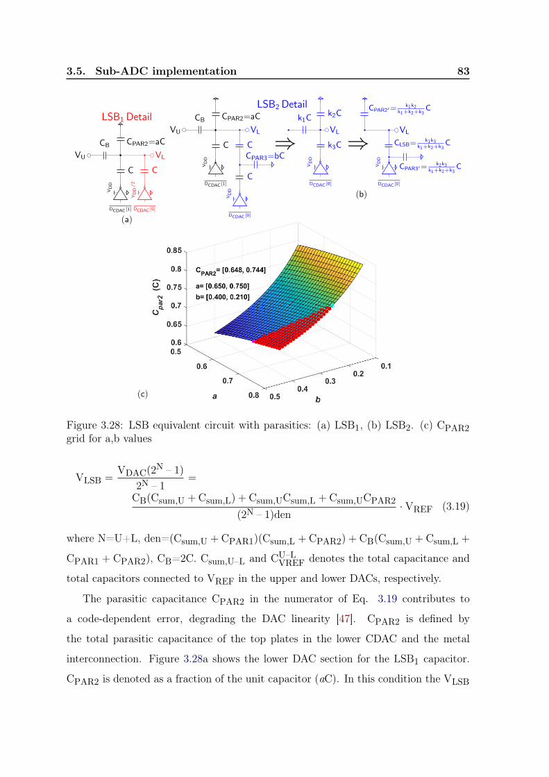
3.5. Sub-ADC implementation 83
(a)
CPAR2=aCCB
VU
C
DCDAC[1]
VDD
LSB1Detail
VL
C
DCDAC[0]
VDD/2
(b)
CPAR2=aCCB
⇒VU
C
DCDAC[1]
VDD
LSB2Detail
VL
CCPAR3=bC
C
DCDAC[0]
VDD
⇒VL
k1Ck2C
k3C
DCDAC[0]
VDD
CPAR2′=k1k2
k1+k2+k3C
VL
CLSB=k1k3
k1+k2+k3C
CPAR3′=k2k3
k1+k2+k3C
DCDAC[0]
VDD
(c)
Figure 3.28: LSB equivalent circuit with parasitics: (a) LSB1, (b) LSB2. (c) CPAR2grid for a,b values
VLSB =VDAC(2
N – 1)
2N – 1=
CB(Csum,U + Csum,L) + Csum,UCsum,L + Csum,UCPAR2
(2N – 1)den· VREF (3.19)
where N=U+L, den=(Csum,U + CPAR1)(Csum,L + CPAR2) + CB(Csum,U + Csum,L +
CPAR1 + CPAR2), CB=2C. Csum,U–L and CU–LVREF denotes the total capacitance and
total capacitors connected to VREF in the upper and lower DACs, respectively.
The parasitic capacitance CPAR2 in the numerator of Eq. 3.19 contributes to
a code-dependent error, degrading the DAC linearity [47]. CPAR2 is defined by
the total parasitic capacitance of the top plates in the lower CDAC and the metal
interconnection. Figure 3.28a shows the lower DAC section for the LSB1 capacitor.
CPAR2 is denoted as a fraction of the unit capacitor (aC). In this condition the VLSB
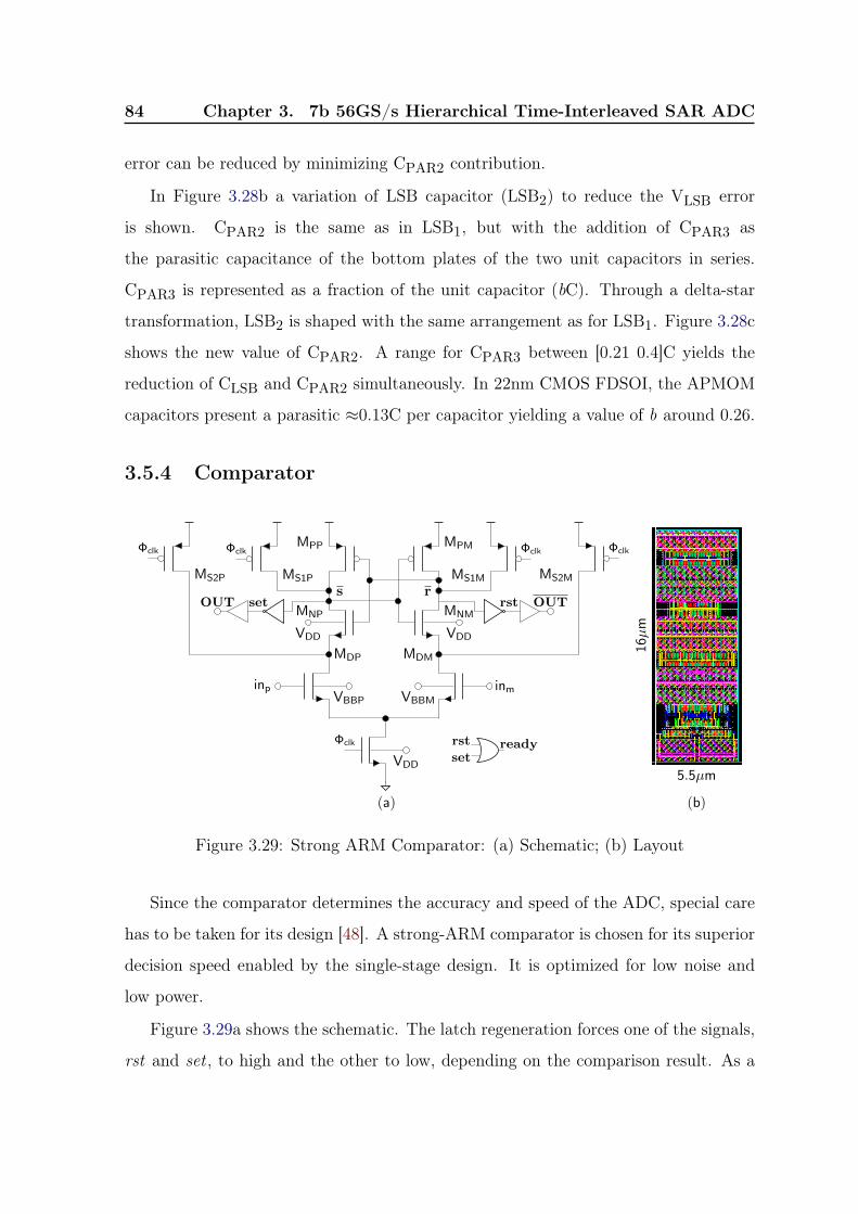
84 Chapter 3. 7b 56GS/s Hierarchical Time-Interleaved SAR ADC
error can be reduced by minimizing CPAR2 contribution.
In Figure 3.28b a variation of LSB capacitor (LSB2) to reduce the VLSB error
is shown. CPAR2 is the same as in LSB1, but with the addition of CPAR3 as
the parasitic capacitance of the bottom plates of the two unit capacitors in series.
CPAR3 is represented as a fraction of the unit capacitor (bC). Through a delta-star
transformation, LSB2 is shaped with the same arrangement as for LSB1. Figure 3.28c
shows the new value of CPAR2. A range for CPAR3 between [0.21 0.4]C yields the
reduction of CLSB and CPAR2 simultaneously. In 22nm CMOS FDSOI, the APMOM
capacitors present a parasitic ≈0.13C per capacitor yielding a value of b around 0.26.
3.5.4 Comparator
inpVBBP
MDP
MNP
VDD
s
MPP
MS1P
Φclk
MS2P
Φclk
VDD
Φclk
inmVBBM
MDM
MNM
VDD
r
MPM
MS1M
Φclk
MS2M
Φclk
5.5µm
(b)(a)
16µm
setOUT rst OUT
readyrst
set
Figure 3.29: Strong ARM Comparator: (a) Schematic; (b) Layout
Since the comparator determines the accuracy and speed of the ADC, special care
has to be taken for its design [48]. A strong-ARM comparator is chosen for its superior
decision speed enabled by the single-stage design. It is optimized for low noise and
low power.
Figure 3.29a shows the schematic. The latch regeneration forces one of the signals,
rst and set , to high and the other to low, depending on the comparison result. As a

3.5. Sub-ADC implementation 85
Figure 3.30: Histogram Strong ARM VOS: Uncalibrated; Calibrated for 100 MC runs
result, the output of the OR gate (ready) is pulled high to enable the asynchronous
control clock and to facilitate the progression to the next step in the SAR conversion.
The offset voltage VOS introduced by the input differential pair is calibrated using
a simple and accurate procedure (appendix B). The calibration operates in two phases:
VOS extraction and VOS calibration. The extraction is a fast loop operating at the
comparator’s clock frequency ΦCLK and follows the Smart Resettable SAR (SR-SAR)
technique presented in [49]. Here, the voltage offset is calculated.
The second phase is a slow loop (below 1MHz), due to the low frequency nature of
the transistor’s back gate. After extracting the VOS, the control block begins to adjust
the threshold voltages (VTH) of the differential pair through a back gate biasing DAC,
which consists of a resistor ladder controlled by a 5-bit digital word.
The nominal voltage supply for the comparator is 0.8V, the same for the back gate
bias at nominal operation. The ladder was designed using a resolution of 5 bits, with
the back gate voltage varying between 0.4 to 0.8V. An artificial offset voltage range of

86 Chapter 3. 7b 56GS/s Hierarchical Time-Interleaved SAR ADC
+/- 32mV ( ≈ 2.1mV steps) was created. For example, if a negative VOS is extracted,
the calibration controller will only choose from the positive range to counterbalance
the negative VOS generated by the differential pair.
Monte Carlo (MC) Post-Layout Simulations (PLS) were performed to calculate the
statistical distribution of VOS and the histograms were plotted in Figure 3.30. The
VOS mean was zeroed and the standard deviation was reduced by a factor of 12.
3.5.5 SAR Logic
Besides the advantage of faster bit-cycle conversion, an additional benefit of
asynchronous SAR logic is that it does not require an external high-frequency clock
and thus saves the power needed to generate and distribute it. This is extremely
important, since this ADC will be part of a time-interleaved system.
The logic of the SAR ADC can be divided into two parts: 1) the clock generation,
which provides the clock for the comparator and the bit-cycle phases and 2) the state
memory, in charge of controlling the CDAC based on the comparator decision in each
of the bit-cycle phases (Figure 3.31). The track duration is set at 25% of the 875MHz
clock period.
The clock generation combines the clock ΦADC, ready and stopcycle signals to
generate the comparator clock (ΦComp) and bit-cycle clocks (CLKp,n) with simple
combinational logic. At the same time, a sampling pulse is generated from ΦADC
and its delay. This pulse propagates sequentially, as controlled by the CLKp,n signals,
generating each of the bit-cycle phases (Figure 3.31). Additionally, the stop cycle
signal is used to indicate the end of the conversion cycle.
The state memory part connects directly to the differential output of the
comparator. A dynamic register is used as memory to optimize loop delay and enables
fast settling upon comparator decision. One cell is activated during every comparison
by its corresponding bitcycle[i] and provides DoutCDAC and DoutCDAC as control
signals for the CDAC. Finally, DoutCDAC is retimed by ΦADC to create the output
data.
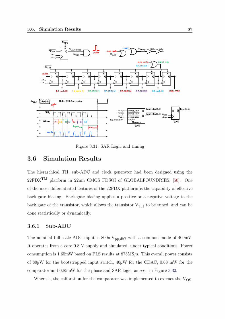
3.6. Simulation Results 87
Figure 3.31: SAR Logic and timing
3.6 Simulation Results
The hierarchical TH, sub-ADC and clock generator had been designed using the
22FDXTM platform in 22nm CMOS FDSOI of GLOBALFOUNDRIES, [50]. One
of the most differentiated features of the 22FDX platform is the capability of effective
back gate biasing. Back gate biasing applies a positive or a negative voltage to the
back gate of the transistor, which allows the transistor VTH to be tuned, and can be
done statistically or dynamically.
3.6.1 Sub-ADC
The nominal full-scale ADC input is 800mVpp,diff with a common mode of 400mV.
It operates from a core 0.8 V supply and simulated, under typical conditions. Power
consumption is 1.65mW based on PLS results at 875MS/s. This overall power consists
of 80μW for the bootstrapped input switch, 40μW for the CDAC, 0.68 mW for the
comparator and 0.85mW for the phase and SAR logic, as seen in Figure 3.32.
Whereas, the calibration for the comparator was implemented to extract the VOS,

88 Chapter 3. 7b 56GS/s Hierarchical Time-Interleaved SAR ADC
50.91%0.85mW
Logic
4.85%0.08mW
Switches
41.82%0.68mW
Comparator
2.42%0.04mW
CDAC
Total=1.65mW
Figure 3.32: sub-ADC power consumption breakdown.
Figure 3.33: Histogram of ADC Output: Uncalibrated, Calibrated for 1000 MC runs
it can also be used to calibrate the ADC. Figure 3.33 shows the MC simulation results.
The ADC was calibrated at the middle of the range (64 LSB) and a 4x reduction of
the output code σ was achieved. It is worth to mention that the limiting factor for the
ADC calibration is the resolution, LSB = 6.25mV (7 bits).
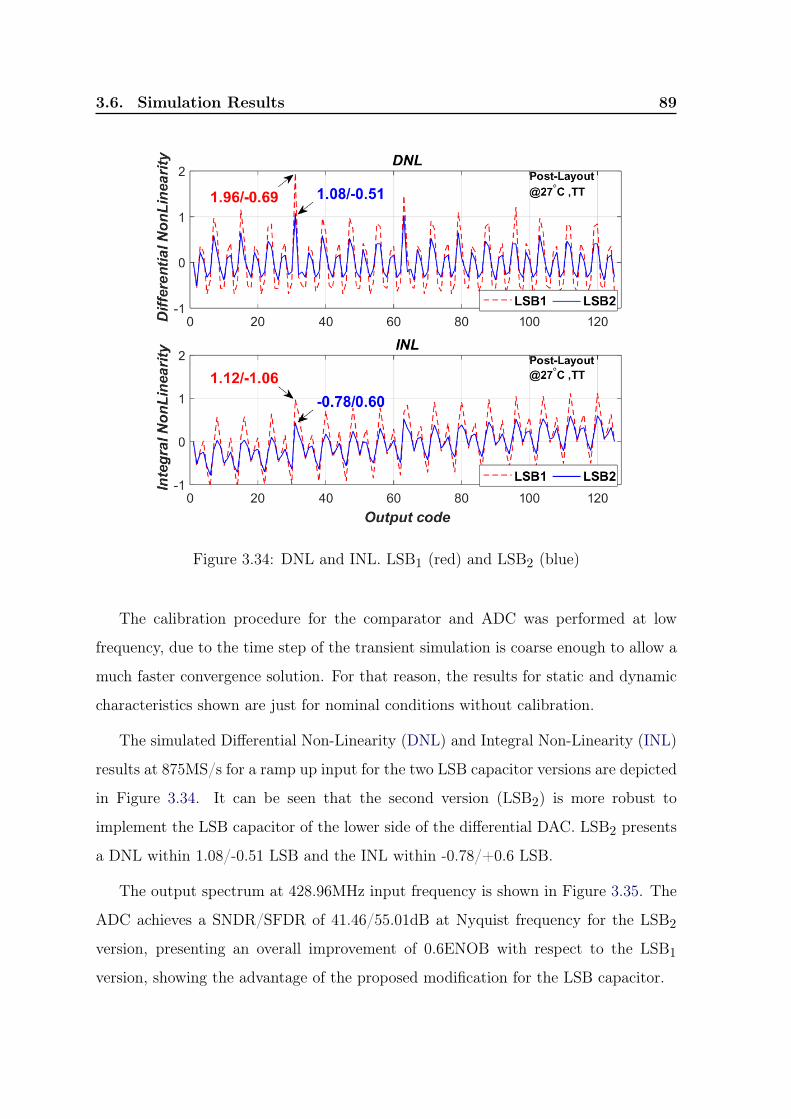
3.6. Simulation Results 89
Figure 3.34: DNL and INL. LSB1 (red) and LSB2 (blue)
The calibration procedure for the comparator and ADC was performed at low
frequency, due to the time step of the transient simulation is coarse enough to allow a
much faster convergence solution. For that reason, the results for static and dynamic
characteristics shown are just for nominal conditions without calibration.
The simulated Differential Non-Linearity (DNL) and Integral Non-Linearity (INL)
results at 875MS/s for a ramp up input for the two LSB capacitor versions are depicted
in Figure 3.34. It can be seen that the second version (LSB2) is more robust to
implement the LSB capacitor of the lower side of the differential DAC. LSB2 presents
a DNL within 1.08/-0.51 LSB and the INL within -0.78/+0.6 LSB.
The output spectrum at 428.96MHz input frequency is shown in Figure 3.35. The
ADC achieves a SNDR/SFDR of 41.46/55.01dB at Nyquist frequency for the LSB2
version, presenting an overall improvement of 0.6ENOB with respect to the LSB1
version, showing the advantage of the proposed modification for the LSB capacitor.
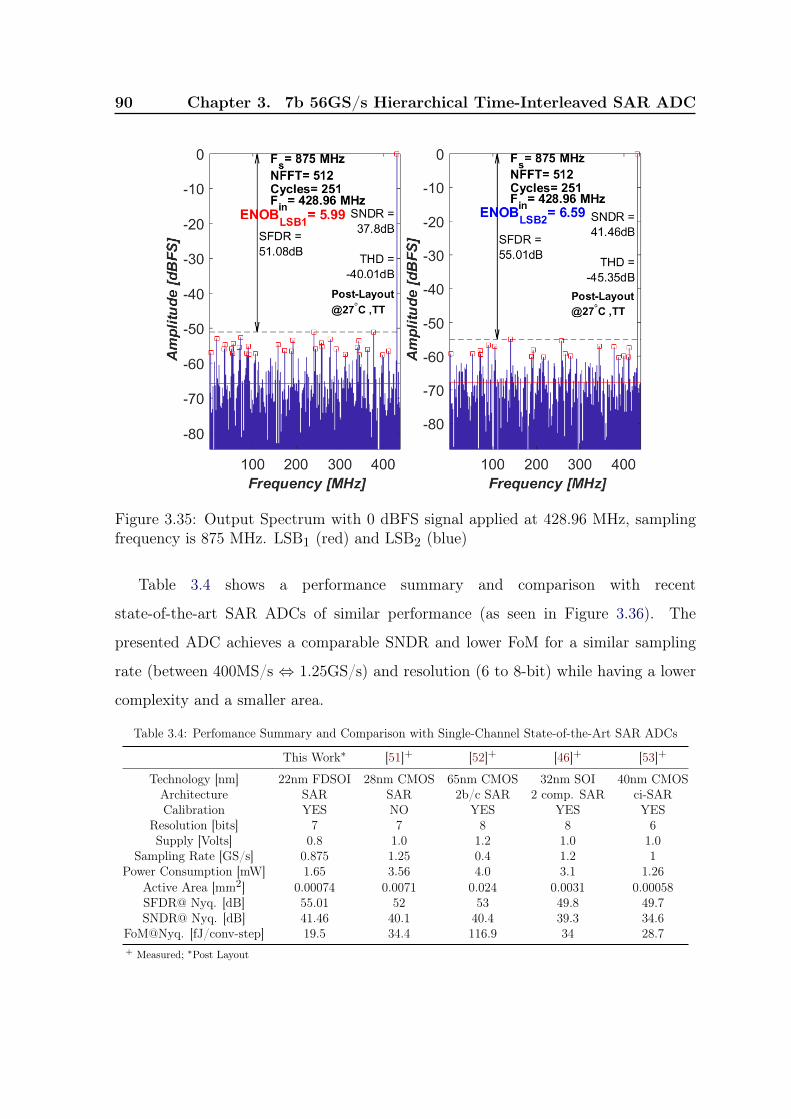
90 Chapter 3. 7b 56GS/s Hierarchical Time-Interleaved SAR ADC
Figure 3.35: Output Spectrum with 0 dBFS signal applied at 428.96 MHz, samplingfrequency is 875 MHz. LSB1 (red) and LSB2 (blue)
Table 3.4 shows a performance summary and comparison with recent
state-of-the-art SAR ADCs of similar performance (as seen in Figure 3.36). The
presented ADC achieves a comparable SNDR and lower FoM for a similar sampling
rate (between 400MS/s ⇔ 1.25GS/s) and resolution (6 to 8-bit) while having a lower
complexity and a smaller area.
Table 3.4: Perfomance Summary and Comparison with Single-Channel State-of-the-Art SAR ADCs
This Work∗ [51]+ [52]+ [46]+ [53]+
Technology [nm] 22nm FDSOI 28nm CMOS 65nm CMOS 32nm SOI 40nm CMOSArchitecture SAR SAR 2b/c SAR 2 comp. SAR ci-SARCalibration YES NO YES YES YES
Resolution [bits] 7 7 8 8 6Supply [Volts] 0.8 1.0 1.2 1.0 1.0
Sampling Rate [GS/s] 0.875 1.25 0.4 1.2 1Power Consumption [mW] 1.65 3.56 4.0 3.1 1.26
Active Area [mm2] 0.00074 0.0071 0.024 0.0031 0.00058SFDR@ Nyq. [dB] 55.01 52 53 49.8 49.7SNDR@ Nyq. [dB] 41.46 40.1 40.4 39.3 34.6
FoM@Nyq. [fJ/conv-step] 19.5 34.4 116.9 34 28.7+ Measured; ∗Post Layout
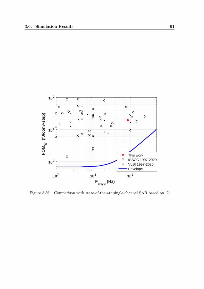
3.6. Simulation Results 91
107 108 109
Fsnyq (Hz)
100
101
102
FO
MW
(fJ
/co
nv-
step
)
This workISSCC 1997-2020VLSI 1997-2020Envelope
Figure 3.36: Comparison with state-of-the-art single-channel SAR based on [2]

92 Chapter 3. 7b 56GS/s Hierarchical Time-Interleaved SAR ADC
3.6.2 TI-ADC
One of the main challenges was to simulate the hierarchical TH and the sub-ADCs in
the same testbench. The sub-ADC has 1 clock domain of 875MHz. A sub-ADC
transient simulation requires a time step of tstep,sub–ADC < 0.02Fs,sub–ADC
≈1UI5 to
guarantee an error tolerance lower than 10–4. The hierarchical TH requires a time
step multiple of its 3 clock domains (28GHz, 3.5GHz and 875MHz). In this case, we
choose the lowest multiple time tstep,TH = 0.0228GHz = 0.01UI for the same accuracy.
Those time steps are valid for separated simulations.
A simulation to obtain the TI-ADC dynamic parameters (SNDR, SDFR, THD)
requires tstep,TH for a simulation time of tstop = ts,sub–ADC×NFFT6. For NFFT=512,
data points require a total time of ≈585ns with time steps of 178.5fs7.
This simulation could take a day or even several days depending of the desired
accuracy. Instead of simulating all the blocks involved in the TI-ADC (sub-ADCs,
hierarchical TH and clock generator) the following approach is taken:
• parameter extraction of the hierarchical TH, sub-ADC and clock generator
relevant to the TI-ADC (resolution, non-linearity and mismatches),
• a simulink model is elaborated using the information of Table 3.5,
• parametric simulations are performed to evaluate the TI-ADC.
Table 3.5 shows the TI-ADC mismatch, static and dynamic error budget. The
static (DNL and INL) and dynamic (SDFR, THD) are taken from the sub-ADC. The
offset, gain error are obtained from the hierarchical TH. The timing error is taken from
the clock generator. The random jitter and dual-dirac jitter are taken from a 28GHz
NRZ CDR clock in 22nm CMOS FDSOI as reference.
Figure 3.37 shows the output spectrum of the SAR-ADC model. The model
includes aperture jitter, DNL, INL, SFDR and THD. The model was implemented to51UI= 1
Fs=17.85ps used as reference time unit6NFFT: Number of data points in the sampling window or FFT7A PLS of the sub-ADC takes ≈4h for dynamic parameters and ≈9h for static parameters to
complete
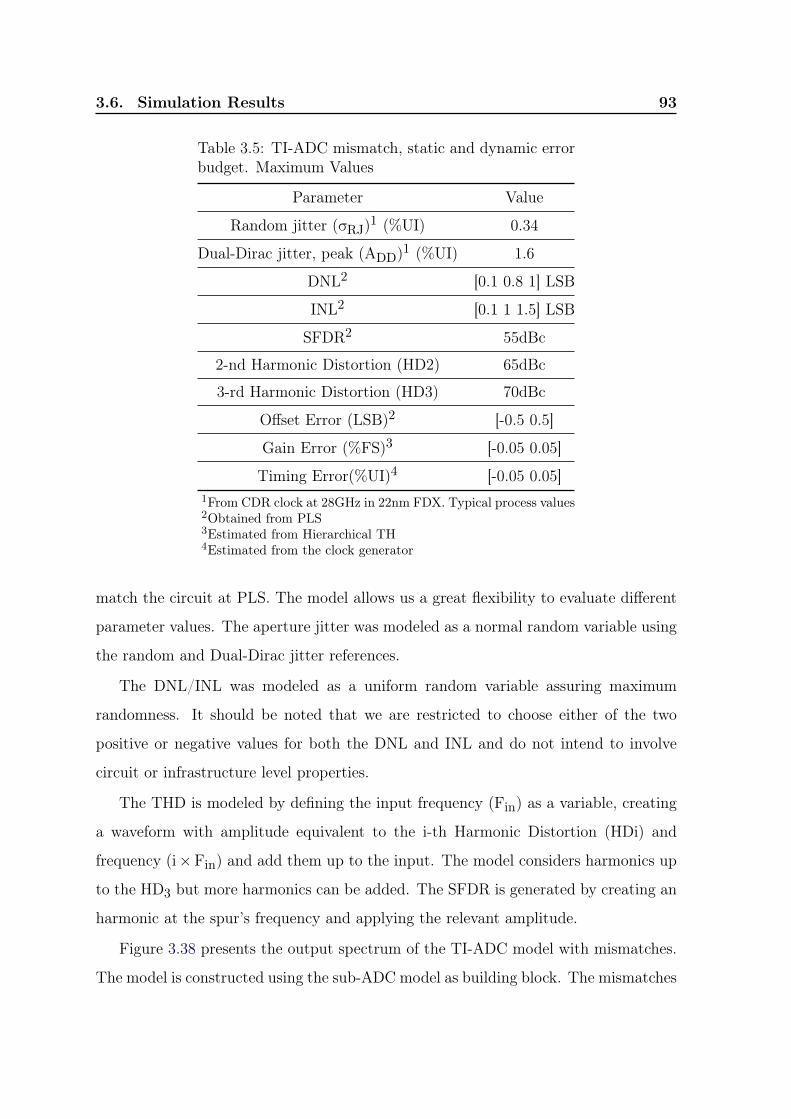
3.6. Simulation Results 93
Table 3.5: TI-ADC mismatch, static and dynamic errorbudget. Maximum Values
Parameter Value
Random jitter (σRJ)1 (%UI) 0.34
Dual-Dirac jitter, peak (ADD)1 (%UI) 1.6
DNL2 [0.1 0.8 1] LSB
INL2 [0.1 1 1.5] LSB
SFDR2 55dBc
2-nd Harmonic Distortion (HD2) 65dBc
3-rd Harmonic Distortion (HD3) 70dBc
Offset Error (LSB)2 [-0.5 0.5]
Gain Error (%FS)3 [-0.05 0.05]
Timing Error(%UI)4 [-0.05 0.05]1From CDR clock at 28GHz in 22nm FDX. Typical process values2Obtained from PLS3Estimated from Hierarchical TH4Estimated from the clock generator
match the circuit at PLS. The model allows us a great flexibility to evaluate different
parameter values. The aperture jitter was modeled as a normal random variable using
the random and Dual-Dirac jitter references.
The DNL/INL was modeled as a uniform random variable assuring maximum
randomness. It should be noted that we are restricted to choose either of the two
positive or negative values for both the DNL and INL and do not intend to involve
circuit or infrastructure level properties.
The THD is modeled by defining the input frequency (Fin) as a variable, creating
a waveform with amplitude equivalent to the i-th Harmonic Distortion (HDi) and
frequency (i×Fin) and add them up to the input. The model considers harmonics up
to the HD3 but more harmonics can be added. The SFDR is generated by creating an
harmonic at the spur’s frequency and applying the relevant amplitude.
Figure 3.38 presents the output spectrum of the TI-ADC model with mismatches.
The model is constructed using the sub-ADC model as building block. The mismatches

94 Chapter 3. 7b 56GS/s Hierarchical Time-Interleaved SAR ADC
Figure 3.37: Output Spectrum for the SAR-ADC model in simulink.
are modeled as uniform random variables. The offset is obtained from the sub-ADC
calibration results and represented in LSB.
The gain mismatches are estimated from hierarchical TH. The total gain variation
is considered as the contribution of the 3 ranks. A gain control of (+/- 25%) in the last
rank was implemented to avoid saturation at the input of the sub-ADC. The timing
mismatches were represented as a percentage of 1UI and estimated from the clock
generator.
The mismatch error values taken for this simulation were conservative. For that
reason, the obtained SNDR of 35dB (ENOB=5.5 bits) can be considered as a good
approximation of the complete TI-ADC behaviour.
A parametric simulation for the different mismatches were performed. Figure 3.40
summarizes the parametric simulation. It compares the ENOB vs DNL/INL for a

3.6. Simulation Results 95
Figure 3.38: Output Spectrum for the TI-ADC model with mismatches.
mismatch parameter set up. The TI-ADC with no mismatches and the default value
of DNL/INL represent the maximum achievable ENOB=5.86 bits. A more realistic
case is represented by the delimited box. The actual value of the ENOB will be found
in this region. Under this condition, a ENOB of 5 bits is expected for a conservative
set of parameters.
The TI-ADC power consumption breakdown is shown in Figure 3.40. It consists
of 113.5mW for the hierarchical TH, 105.6mW for the 64 sub-ADCs and 69.6mW for
the clock generator. The circuits were designed to optimize power and the power
constraint of 500mW was maintained.
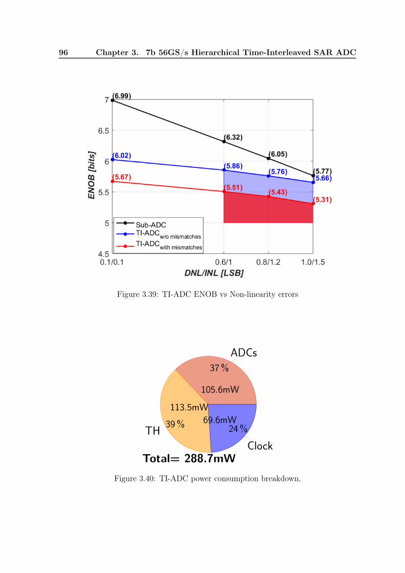
96 Chapter 3. 7b 56GS/s Hierarchical Time-Interleaved SAR ADC
Figure 3.39: TI-ADC ENOB vs Non-linearity errors
37%
105.6mW
ADCs
39%
113.5mW
TH 24%69.6mW
ClockTotal= 288.7mW
Figure 3.40: TI-ADC power consumption breakdown.

3.7. Conclusion 97
3.7 Conclusion
In this chapter, we have presented the design of a high speed TI-ADC. A design flow
was introduced to breakdown the principal aspects of the design:
1. The use of hierarchical sampling can optimize the number of low-jitter clock
signals and simplify the distribution of non-critical clocks,
2. The suppression and calibration of DCD have been implemented for the low-jitter
clocks,
3. The design using the 22FDXTM platform allows a power efficient design and
flexible design through back gate biasing,
4. The designed sub-ADC design has achieved,
• A power- and area-efficient 7-bit 875MS/s SAR ADC has been
demonstrated,
• An improvement for the CDAC LSB capacitor allows a substantial
improvement in the SNDR,
• A simple and accurate calibration procedure for the comparator and ADC
is presented.
5. The TI-ADC design has demonstrated that:
• A fast and accurate simulink model was developed to evaluate the design
and speed up the simulations,
• An ENOB above 5 bits can be expected using a conservative set of static,
dynamic and mismatches parameters.
These results demonstrated an optimized TI-ADC design with medium
resolution that supports 56GS/s operation.

Chapter 4
ADC-RX prototype andprospects
Contents4.1 ADC-RX prototype . . . . . . . . . . . . . . . . . . . . . . . . . 99
4.1.1 Top-level diagram . . . . . . . . . . . . . . . . . . . . . . . . . . 99
4.1.2 Chip layout . . . . . . . . . . . . . . . . . . . . . . . . . . . . . . 108
4.2 Prospects . . . . . . . . . . . . . . . . . . . . . . . . . . . . . . . 114
4.2.1 Chip Tapeout . . . . . . . . . . . . . . . . . . . . . . . . . . . . . 114
4.2.2 Speed augmentation and improvements . . . . . . . . . . . . . . 115
4.3 Conclusion . . . . . . . . . . . . . . . . . . . . . . . . . . . . . . . 119

4.1. ADC-RX prototype 99
Chapter 4 presents the physical implementation of an ADC-based receiver prototype
in 22nm CMOS FDSOI technology. It includes the TI-ADC developed in chapter 3
and other blocks that complete the design. A testbench to perform characterization of
the receiver and several aspects to improve the current design are discussed.
4.1 ADC-RX prototype
4.1.1 Top-level diagram
A chip prototype called ADC-RX is prepared. Figure 4.1 shows the top-level diagram
of the prototype. The design implements an ADC-based receiver consisting of:
• An AFE consisting of a CTLE for pre-equalization and gain boosting. It includes
a 50Ω matching, offset and gain calibration,
• A 56GS/s 64-way 7-bit SAR TI-ADC. It includes offset and gain calibration,
• A clock generator for the TI-ADC and digital controller. It generates all the
required clocks from an external signal clock of 28GHz,
• A retimer to resample the TI-ADC outputs into a single clock domain. Special
considerations are taken to keep aligned the samples in the correct order,
• A 64kbits SRAM memory to store 8192 samples (7-bit per sample). The memory
is made out of 16kbits from the IP provider INVECAS,
• A Digital Controller for calibration and memory control. It includes an array of
registers for calibration and the I2C protocol for off-chip interface.

100 Chapter 4. ADC-RX prototype and prospects
Figure 4.1: Diagram of 112 Gb/s PAM4 ADC-based receiver.
The top level diagram of AFE is shown is Figure 4.2. It is composed of 3 main
blocks: a 50Ω termination, a CTLE and a back gate biasing DAC.
−
+−+
Vin,p
Vinm
VREFCMinp
inm
VCM
Voutp
Voutm
CTLE50Ω
Termination
Ladenable
Ladcode[5:0]
VB
BP
VB
BN
BodyBiasing
DAC
CA
LRL[3
:0]
CA
LRS[3
:0]
CA
LTANK[4
:0]
Figure 4.2: CTLE top diagram.

4.1. ADC-RX prototype 101
The 50Ω termination is an input passive matching network to compensate the
parasitic capacitance from the PAD. It employs a custom built T-coil inductor for
high frequency peaking (as seen in Figure 4.3a).
A CML-based CTLE stage to provide pre-equalization and signal conditioning
to the input of the TI-ADC (as seen in Figure 4.3b). It uses a source degenerated
differential pair to achieve high frequency peaking. It has the following features:
• An input Common Mode Feedback (CMFB) circuit to control the common mode
voltage at the input,
• A programmable high-frequency peaking gain trough the load resistance RL and
source resistance (RS) using a 4-bit word control,
• A programmable peaking frequency (28GHz) using a 5-bit RC-tank (Rtank and
Ctank) and a custom built inductor load L,
• Offset mismatch calibration using back gate biasing through 5-bit resistor DAC
Vin,p
Wn
L
VBBP
L
RL
Vout,m
RS
Vin,m
Wn
L
VBBM
L
RL
Vout,m
RS
RCM RCMVCM
Ctank
Rtank
Ctank
Rtank
Vtank
Tank[4 : 0]
120Ω ± 20%︸ ︷︷ ︸RL[3:0]
75Ω ± 20%︸ ︷︷ ︸RS[3:0]
(b)
inp
50Ω
50Ω
inm
vcm
outp
outm
(a)
Tcoil
Tcoil
Figure 4.3: (a) 50Ω termination circuit. (b) Schematic diagram.

102 Chapter 4. ADC-RX prototype and prospects
(see Appendix B.1.3).
• A variable supply voltage with 1V of nominal value. The CTLE output defines
the input common mode of the rank-1 buffer.
The CTLE simulation parameters at nominal corner are summarized in Table 4.1.
The input common mode of 0.56V is controlled by the input CMFB circuit to fix a
voltage of 0.3V across the source resistors RS. The differential pair requires a minimum
VDS of 450mV to keep a good linearity. This generates an output common mode of
0.75V for the input transistors of the rank-1 buffer.
Due to the fact that the CTLE was designed after the hierarchical TH, a change
in the input transistors of the rank-1 buffer was required. The reason behind it was
to keep the same output common mode of 0.35V for the buffers while having an
increment of ≈120mV in the input common mode. The transistors were change to
the standard Vt (SVT) NMOS in order to keep the same transconductance efficiency
Table 4.1: CTLE Parameters atNominal Corner (T=27C)
Supply 1V
Input Common Mode1 0.56V
Output Common Mode2 0.75V
Load resistance (RL) 120Ω
Source resistance (RS) 75Ω
Resistor Code3 8
Tank Code3 31
DC gain -12dB
Peaking gain4 11.5dB
Peaking gain frequency5 33GHz
Power Consumption 11.5mW1Controled by the input CMFB2Required for linearity3Default values44-bit DAC calibration55-bit DAC calibration

4.1. ADC-RX prototype 103
(gm/ID). Thus, the buffer speed or power consumption were not altered.
The CTLE stage was designed to have a constant-DC gain (≈-12dB) and a
programmable peaking gain (up to 12.5dB) controlled by RL and RS. The peaking
gain frequency is programmable too (up ≈41GHz ) and is controlled by the RC-tank.
Compared with a constant peaking gain CTLE (with programmable DC gain), the
constant-DC gain CTLE can either reduce the required gain of the hierarchical TH at
high-loss channels and/or improve the linearity of rank-1 buffer at low-loss channels.
Figure 4.4 presents the CTLE transfer function for the nominal, slow and fast
corners for the resistor and RC tank default codes of 8 and 31, respectively. A CTLE
design with minimum parameters variation is demonstrated for the worst case corners
and temperature. The programmability of the peaking gain and frequency of the CTLE
is shown in Figures 4.5 and 4.6, respectively. A range variation of ≈2dB with linear
increment steps of 0.29dB is achieved for the peaking gain. The peaking frequency
starting in 33GHz can be programmed up to 41.67GHz with linear steps of 0.27GHz.
107 108 109 1010 1011
Frequency (Hz)
-14
-12
-10
-8
-6
-4
-2
0
2
Hs,
CT
LE (
dB
)
RES CODE =8
TANK CODE =31
DC Gain=[ -12.41 -11.85 ] dB
Peaking Frequency=[ 31.62 34.67 ] GHz
Peaking Gain=[ 10.27 12.56 ] dB
NOMINALSLOW
@125°CFAST
@-40°C
CORNER
Figure 4.4: CTLE transfer function for nominal, slow and fast corners

104 Chapter 4. ADC-RX prototype and prospects
107 108 109 1010 1011
Frequency (Hz)
-14
-12
-10
-8
-6
-4
-2
0
2 H
s,C
TL
E (
dB
) TANK CODE =31
DC Gain=[ -12.04] dB
Peaking Frequency= 33.11 GHz
Peaking Gain= 11.55 dB +/- 1dB
CODE=8CODE=0CODE15
RESISTOR CODE
Figure 4.5: Programmability of the peaking gain
107 108 109 1010 1011
Frequency (Hz)
-14
-12
-10
-8
-6
-4
-2
0
Hs,
CT
LE (
dB
)
RES CODE =8
DC Gain=[ -12.06] dB
Peaking Frequency=[ 33.11 41.69 ] GHz
Peaking Gain=[ 11.23 7.76 ] dB
CODE=31CODE=0CODE15
TANK CODE
Figure 4.6: Programmability of the peaking frequency

4.1. ADC-RX prototype 105
The retimer receives the outputs from the TI-ADC and aligns the multi-phased
sub-ADCs outputs into a single 875MHz clock domain. These retimed outputs are
stored in a 64kbits SRAM (8912 samples/7-bit per sample). An important aspect to
take in consideration is the selection of the clock phase. It will determine the order
of stored samples. The ADC clock domains are spread every UI (1UI=17.86ps) and
therefore cannot be resampled directly using a single clock phase. As a matter of fact,
if a setup of 2UI and a hold of 1UI need to be maintained for the resampling FFD, any
of the ADC clocks will violate this condition. Two cases for the retimer clock phase
were evaluated.
For instance, in the first case, if using the clock of ADC[0], sampling directly the
outputs of ADC 1 to 60 is possible but ADC 61, 62, 63 and 0 will be updating their
samples during the aperture time of the FF. In order to mitigate this timing violation,
an intermediate clock can be used to stretch the validity of these 4 ADC outputs by
inserting an extra FFD and hence guarantee steady outputs when finally resampling
using clock of ADC[0]. The intermediate clock domain could be anything between 2
and 60. The net result of this resampling scheme is that the sample order will become
61, 62, 63, 0, 1, . . . 60. The first case using ADC[0] clock is summarized as:
• Direct samples: 1 to 60 retimed with phase [0],
• Indirect samples: 61, 62, 63 and 0 retimed with phase [0] and intermediate clock
phase between [4:57],
• Retimer sample order: 61, 62, 63, 0, 1, 2 . . . 57, 58, 59 and 60.
Analyzing this reshuffling, it can be shown that by selecting ADC[3] to start with,
we can get the ADC samples in the right order:
• Direct samples: 4 to 63 retimed with phase [3],
• Indirect samples: 0, 1, 2 and 3 retimed with phase [3] and intermediate clock
phase between [7:62],
• Retimer sample order: 0, 1, 2, 3, 4, 5 . . . 60, 61, 62 and 63.
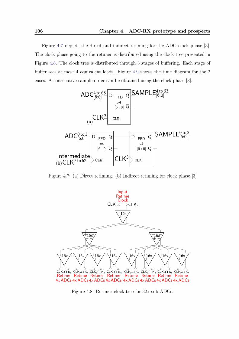
106 Chapter 4. ADC-RX prototype and prospects
Figure 4.7 depicts the direct and indirect retiming for the ADC clock phase [3].
The clock phase going to the retimer is distributed using the clock tree presented in
Figure 4.8. The clock tree is distributed through 3 stages of buffering. Each stage of
buffer sees at most 4 equivalent loads. Figure 4.9 shows the time diagram for the 2
cases. A consecutive sample order can be obtained using the clock phase [3].
CLK
Q
D QFFD
x4[6 : 0]
ADC4 to 63[6:0]
SAMPLE4 to 63[6:0]
CLK3
(a)
CLK
Q
D QFFD
x4[6 : 0]
CLK
Q
D QFFD
x4[6 : 0]
ADC0 to 3[6:0]
SAMPLE0 to 3[6:0]
IntermediateCLK7 to 62 CLK3
(b)
Figure 4.7: (a) Direct retiming. (b) Indirect retiming for clock phase [3]
16x
16x 16x
CLKnCLKp
InputRetimeClock
16x 16x 16x 16x 16x 16x 16x 16x
CLKpCLKn CLKpCLKn CLKpCLKn CLKpCLKn CLKpCLKn CLKpCLKn CLKpCLKn CLKpCLKn
Retime4xADCs
Retime4xADCs
Retime4xADCs
Retime4xADCs
Retime4xADCs
Retime4xADCs
Retime4xADCs
Retime4xADCs
−++ −
−++ −
−++ −
−++ −
−++ −
−++ −
−++ −
−++ −
−++ −
−++ −
−++ −
Figure 4.8: Retimer clock tree for 32x sub-ADCs.

4.1. ADC-RX prototype 107
sub-ADC
phase
DataTransition=17.86psor
1UI
FFDset-up=2UI
holdtime=
1UI
Directretime
↓Directretime
↓61,62,63and0
︷︸︸
︷IndirectRetim
e[4
:57]
↑Indirectretime
↑Indirectretime
Retim
ersample
order:61,62,63,0,
1,2,
3,...
sub-ADC
phase
Directretime
↓Directretime
↓0,1,2
and3
︷︸︸
︷IndirectRetim
e[7
:62]
↑Indirectretime
x Indirectretime
Retim
ersample
order:0,
1,2,
3,...60,
61,62
and63
875M
Hz [0]
5657
5859
6061
6263
01
23
45
67
89
1011
1213
1415
1617
1819
20
875M
Hz [3]
5657
5859
6061
6263
01
23
45
67
89
1011
1213
1415
1617
1819
20
Figure4.9:
Tim
ingDiagram
oftheRetim
er.

108 Chapter 4. ADC-RX prototype and prospects
4.1.2 Chip layout
In this subsection, we discuss the physical implementation of the internal blocks of the
ADC-RX chip. The AFE layout is depicted in Figure 4.2. The layout is implemented
to have a full symmetry on the vertical axis. It includes:
• The 50Ω termination, where the T-coil inductors occupied most of the area,
• The CTLE core includes the NMOS differential pair, RL, RS and the RC-tank.
Closely to the 50% of area is occupied by the programmable RC-tank,
• The decoders for RL, RS and RC-tank. They are composed by a static logic cells
which takes the input word control and enables the programmable peaking gain
and frequency.
Additionally, an empty space at the output of the CTLE is left for the buffer of
rank-1 to minimize interconnection routing. The complete layout occupies an active
area of 99μm× 143μm and is shown in Figure 4.10.
143µm
99µm
Space for therank-1 buffer
50ΩTermination
CTLECORE
RL
Decoder
RS
Decoder
RC-TANKDecoder
Figure 4.10: CTLE layout.

4.1. ADC-RX prototype 109
The floorplanning of the TI-ADC is presented in Figure 4.11. The layout was
implemented using the following guidelines:
• The samplers, gain stages and ADCs were placed according to the clock phase
in each TH rank,
• A symmetrical metal routing was implemented to guarantee the same delay
between consecutive ranks,
• The even and odd clock phases were formed in 2 groups per rank. In this way
the output interconnection between ranks was minimized,
• The ADCs were placed in 2 rows of 32 each in order to avoid a large metal
connection to the ADCs on the sides,
• A space between the ADCs rows was reserved to the retimer and clock signal
routing,
• The right side routing was reserved for high speed routing (clock signals) and
the left side for low frequency routing (biasing, calibration and ATP).
The TI-ADC layout is depicted in Figure 4.12. It shows each of the 3 ranks of the
hierarchical TH and the 2 rows of 32x ADCs. The calibration, current reference and
Analog Test Point (ATP) signals were routed on the left side while the clock signals
for each rank on the left.
The retimer and the complete TI-ADC occupy an active area of 40μm × 417μm
and 296μm× 425μm, respectively.
[0][1] Rank-1 CLOCKPHASES
[0][2][4][6][8][10][12][14][1][3][5][7][9][11][13][15] Rank-2 CLOCKPHASES
[0][2][4][6][8][10][12][14] [16][18][20][22][24][26][28][30][1][3][5][7][9][11][13][15] [17][19][21][23][25][27][29][31]
[32][34][36][38][40][42][44][46] [48][50][52][54][56][58][60][62][33][35][37][39][41][43][45][47] [49][51][53][55][57][59][61][63]
ADCs CLOCKPHASES
Figure 4.11: TI-ADC Floorplanning.

110 Chapter 4. ADC-RX prototype and prospects
425µm
296µ
m
1 rank-12 rank-2
417µm20µm
12
rank-3
32xADC
Clock treeRetimer
32xADC
RetimerClock tree
Figure 4.12: 7-bit 56GS/s 64-Way TI-ADC layout.
The clock generator layout is shown in Figure 4.13a. It occupies an active area
of 88μm × 331μm. The layout was placed on the lower right side of the TI-ADC. Its
position relative to the rank samplers was chosen to minimize the metal routing for
the rank-1 and rank-2. Thick metals layers were used to route the clock signals going
to the samplers and ADCs.
The layout floorplan was organized to leave room for routing and enable sufficient
space between adjacent clock signals for parasitic coupling capacitance reduction. The
clock buffers were designed to optimize delay. The parasitic capacitance load was

4.1. ADC-RX prototype 111
extracted from layout and modeled as a differential transmission line.
Figure 4.13b depicts the ADCs clock routing. The clock generator was placed to
the bottom right of the TI-ADC closer to rank-1 and rank-2. Its is shown the clock
distribution going to the 2 rows of 32x ADCs coming from rank-3. Special attention
was taken to match all the clock routing paths to have the same parasitic routing
capacitance. Thus, all paths present the same delay.
331µm
88µm
(a)
(b)
Inputto rank-1 Div4
to rank-2Divider by 8
to rank-3
Retimer
TI-ADC(32x ADCs)Retimer
TI-ADC
ClockGenerator
MatchedADCs
Clock Routing
Figure 4.13: (a) Clock generator layout. (b) ADCs clock routing detail

112 Chapter 4. ADC-RX prototype and prospects
The ADC-RX chip was implemented in 22nm CMOS FDSOI. It is composed by
the following structures and characteristics:
• It is a PAD limited design with a total of 44 PADs. The aspect ratio is 1 with 11
PADs per side. The top PAD row corresponds to the I2C interface with digital
IOs. The input signal and external clock are located in the bottom row. The
voltage supplies and ground are placed in the lateral pad rows,
• The biasing generates source and sink currents of 500μA, 250μA and 50μA from
a low TC (≤58-ppm/C) 10μA current source reference. The current reference is
generated using a sub-1V bandgap voltage reference. It occupies an active area
of 218μm× 429μm,
• The calibration ladders generate the back gate biasing control. It presents 4
modes of configuration using ground, 0.8V and 1.6V references. It occupies an
active area of 150μm× 175μm,
• The CTLE as pre-equalizer. It includes a common mode voltage reference VCM.
It occupies an active area of 118μm× 143μm,
• The TI-ADC and retimer for data conversion. They occupy an active area of
345μm× 425μm,
• The clock generator occupies an active area of 88μm× 331μm,
• A High Density Single-Port SRAM cell-based Register File Memory Compiler
from INVECAS. The size is 64kbits (7 bits x 8192 is the requirement = 57.3kbits)
made out of 4 units of 16kbits. It is implemented with a high density 0.11088μm2
bit cell,
• A programmable frequency ring oscillator and Power-on-Reset (POR) unit for
the digital controller. They occupy an active area of 7.5μm× 24μm and 29μm×159μm, respectively,
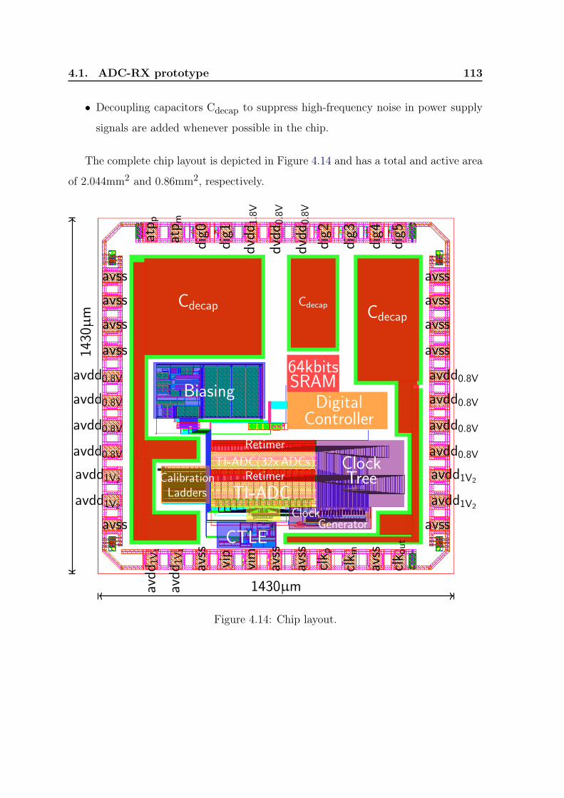
4.1. ADC-RX prototype 113
• Decoupling capacitors Cdecap to suppress high-frequency noise in power supply
signals are added whenever possible in the chip.
The complete chip layout is depicted in Figure 4.14 and has a total and active area
of 2.044mm2 and 0.86mm2, respectively.
1430µm
1430µm
Cdecap CdecapCdecap
64kbitsSRAM
DigitalController
Biasing
CalibrationLadders
CTLE
TI-ADC
TI-ADC(32xADCs)Retimer
Retimer
ClockGenerator
ClockTree
avss avss
avss avss
avss avss
avss avss
avdd0.8V avdd0.8V
avdd0.8V avdd0.8V
avdd0.8V avdd0.8V
avdd0.8V avdd0.8V
avdd1V2avdd1V2
avdd1V2avdd1V2
avss avss
avdd
1V1
atp p
avdd
1V1
atp m
avss
dig0
vip
dig1
vim
dvdd
1.8V
avss
dvdd
0.8V
avss
dvdd
0.8V
clk p
dig2
clk m
dig3
avss
dig4
clk o
ut
dig5
Figure 4.14: Chip layout.
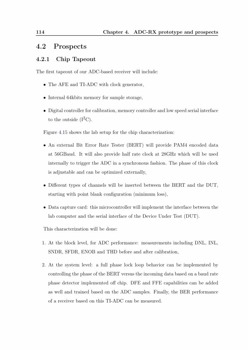
114 Chapter 4. ADC-RX prototype and prospects
4.2 Prospects
4.2.1 Chip Tapeout
The first tapeout of our ADC-based receiver will include:
• The AFE and TI-ADC with clock generator,
• Internal 64kbits memory for sample storage,
• Digital controller for calibration, memory controller and low speed serial interface
to the outside (I2C).
Figure 4.15 shows the lab setup for the chip characterization:
• An external Bit Error Rate Tester (BERT) will provide PAM4 encoded data
at 56GBaud. It will also provide half rate clock at 28GHz which will be used
internally to trigger the ADC in a synchronous fashion. The phase of this clock
is adjustable and can be optimized externally,
• Different types of channels will be inserted between the BERT and the DUT,
starting with point blank configuration (minimum loss),
• Data capture card: this microcontroller will implement the interface between the
lab computer and the serial interface of the Device Under Test (DUT).
This characterization will be done:
1. At the block level, for ADC performance: measurements including DNL, INL,
SNDR, SFDR, ENOB and THD before and after calibration,
2. At the system level: a full phase lock loop behavior can be implemented by
controlling the phase of the BERT versus the incoming data based on a baud rate
phase detector implemented off chip. DFE and FFE capabilities can be added
as well and trained based on the ADC samples. Finally, the BER performance
of a receiver based on this TI-ADC can be measured.
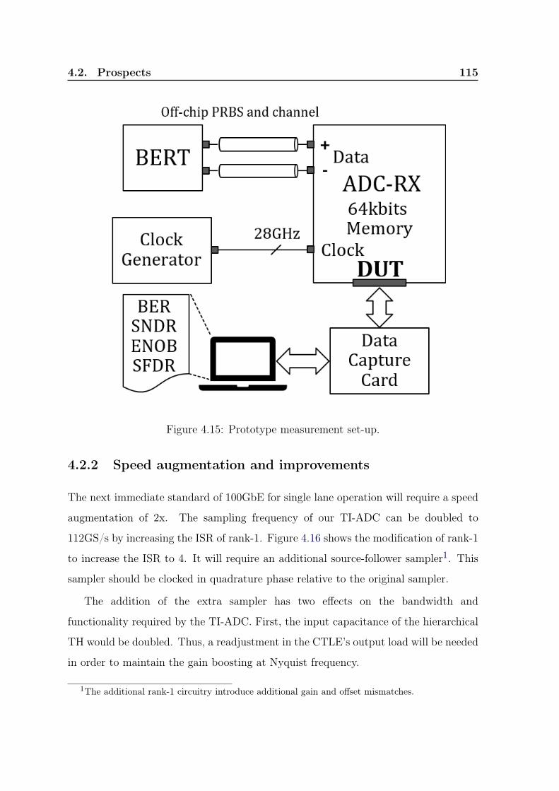
4.2. Prospects 115
Figure 4.15: Prototype measurement set-up.
4.2.2 Speed augmentation and improvements
The next immediate standard of 100GbE for single lane operation will require a speed
augmentation of 2x. The sampling frequency of our TI-ADC can be doubled to
112GS/s by increasing the ISR of rank-1. Figure 4.16 shows the modification of rank-1
to increase the ISR to 4. It will require an additional source-follower sampler1. This
sampler should be clocked in quadrature phase relative to the original sampler.
The addition of the extra sampler has two effects on the bandwidth and
functionality required by the TI-ADC. First, the input capacitance of the hierarchical
TH would be doubled. Thus, a readjustment in the CTLE’s output load will be needed
in order to maintain the gain boosting at Nyquist frequency.
1The additional rank-1 circuitry introduce additional gain and offset mismatches.

116 Chapter 4. ADC-RX prototype and prospects
The second effect is the group delay of the two source-followers samplers may no
longer match. This will require a timing correction of the quadrature clock fed to the
additional sampler. This correction can be implemented using a phase interpolator.
Vin
BF1
28GHz0
28GHz180
Cs1
Cs1
BF2
BF2
to rank-2. . .
to rank-2. . .
BF1
28GHz90
28GHz270
Cs1
Cs1
BF2
BF2
to rank-2. . .
to rank-2. . .
1 : 4
Rank− 1
28GHz 0
28GHz 90
28GHz 180
28GHz 270
Figure 4.16: Modification of rank-1 to extend the design to 112GS/s
Power savings in the current hierarchical TH can be implemented. The power
consumption of the OpAmps in the gain stage of rank-3 can be reduced by changing
the direct (or Miller) compensation method. OpAmps using indirect feedback
compensation technique have shown faster and low-power designs [54].
Figure 4.17 shows a new version for the OpAmp in rank-3. This topology uses
split-length load devices in the first stage. The compensation capacitor CC is connected
to the internal low impedance node-A to achieve indirect compensation.
Pole splitting can be obtained with a lower value of CC and gm6. This results in
a faster, more compact and lower power OpAmp when compared to the traditional
Miller compensation.

4.2. Prospects 117
M1AinpM1B
inm
VBP M5
VBB1
M2A
VBB1
VOCMFB
VBB1
M2B
VBB1
M6A
outp
VBBP
RZ Cc
VBPM7A
M6B
outm
VBBM
RZCc
VBP M7B
A A′
Figure 4.17: A two-stage OpAmp with indirect feedback compensation usingsplit-length load devices.
A new version of this chip envisioned a complete redesign of the circuits in the AFE
and hierarchical TH. Inverter-based circuits have shown potential for area reduction
while maintaining low power. These circuits take full advantage of technology scaling.
Inverters as analog transconductors have been studied in [55, 56]. Figure 4.18 shows
different inverter-based circuits. Inverter-based active inductors can be used to replace
the area-consuming passive inductors as well.
An inverter-based CTLE for PAM2 at 56Gb/s has been demonstrated in 16nm
FinFET CMOS [57]. Recently, a 112Gb/s PAM4 LR wireline transceiver in 7nm
FinFET CMOS has been published. It includes an inverter-based AFE in the receiver
[26].
An inverter-based CTLE circuit is shown in Figure 4.19. It consists of a low and
high gain paths and uses a feedforward coupling capacitor (Cz) to sum the currents
from both paths. The DC and peaking gain are determined by the transconductance
of the inverters and can be fully configurable. These circuit serves as an example for
a new class of area and power efficient circuits in newer technology nodes.

118 Chapter 4. ADC-RX prototype and prospects
VinGm Gm
Vout
Unity Gain Buffer
VinGm Gm
Vout
Pole Buffer
CL
VinαGm Gm
Vout
Programmable Gain
Vin,1Gm Gm
Vout
Vin,2Gm
Summing
Vin Vout
Inverter active Inductor
⇒R
⇒Gm
R
Cgs Gds
Vin Vout
⇒1/Gm
R/ωTVin Vout
Figure 4.18: Inverter configurations for different analog blocks.
gm2 gmL
Cz
Vin
gm1 gmL
Vout
DCgain= gm1
gmL
Peaking gain= gm1+gm2
2gmL
Figure 4.19: Inverter-based single ended CTLE schematic.

4.3. Conclusion 119
4.3 Conclusion
An ADC-based receiver prototype in 22nm CMOS FDSOI as proof-of-concept has
been presented. The prototype includes several features such as:
• A CML-based CTLE as pre-equalizer in the AFE with peaking gain and
frequency reconfiguration,
• A 56GS/s 7-bit SAR TI-ADC. It includes calibration for gain, offset and timing
mismatches,
• A 64kbits SRAM to store 8192 samples (7-bit per sample),
• A digital controller unit for memory control and calibration using I2C for off-chip
interface.
Additionally, several enhancements for the current architecture have been proposed.
These improvements aim to increase the total sampling frequency and reduce power
consumption.
This prototype will allow us to verify our ADC-based receiver design for
LR applications at 112Gb/s.
Conclusion
As mixed-signal architectures become more popular for the next-generation of
high-speed serial links with >100Gb/s data rate and multi-level modulation, a specific
design methodology is required. This methodology should define and validate the
requirements and specifications for silicon-based wireline receivers that comply with
>100Gb/s operation over transmission channels with high losses (>20dB).
A revision of the different aspects in wireline communications such as the
100 Gigabit Ethernet Standard, signal modulation, channel selection, equalization
techniques and the state-of-the-art in Chapter 1 allow the definition of specifications
for a PAM4 ADC-based receiver compatible with 100Gb/s operation.
Chapter 2 has presented the methodology to validate the proposed receiver’s
specifications using link system analysis. The transmitter, channel and receiver were
modeled in MATLAB Simulink to complete the high-speed serial link. The receiver
model includes an AFE, an ADC and a DSP unit for equalization. The link was tested
using a PRQS sequence as a test pattern for PAM4. The BER was calculated from
the output sequence of the receiver. It was demonstrated the feasibility of a PAM4
ADC-based receiver with 112Gb/s data rate and channel losses up to 30dB.
Chapter 3, the design of a 56GS/s TI-ADC in 22nm CMOS FDSOI for ADC-based
wireline receivers is presented. A design flow was introduced to breakdown the key
aspects of the design. The design procedure was divided in 3 parts: the hierarchical
TH, the clock generation and the sub-ADC design.
The number of TH stages were chosen to minimize the number of low-jitter
clocks. The circuit was designed following the transconductance efficiency (gm/ID)
methodology using pre-computed lookup tables in MATLAB. The TH sampling clocks
were designed from an external clock signal of 28GHz. A SAR ADC was chosen as
sub-ADC unit for its speed and power efficiency. An improvement for the CDAC
LSB capacitor implementation was described. A simple and accurate calibration
methodology was introduced for the comparator and the ADC. A fast and accurate

simulink model for the TI-ADC was developed to validate the design and to speed up
the simulation time. It is demonstrated a TI-ADC with 56GS/s data rate and ENOB
above 5 bits using a conservative set of static, dynamic and mismatches parameters.
Chapter 4 is dedicated to the ADC-based receiver prototype in 22nm CMOS FDSOI
technology. It includes a CML-based CTLE for pre-equalization, a 56GS/s 7-bit SAR
TI-ADC, a 64kbits SRAM for sample storage, a digital controller for memory control
and calibration using I2C for off-chip interface. A procedure for chip characterization
to evaluate the TI-ADC and BER performance is proposed. This prototype will allow
the verification of the proposed ADC-based receiver at 112Gb/s.
Additionally, several enhancements for the current architecture have been proposed.
These improvements aim to increase the total sampling frequency and reduce power
consumption.

Publications
International Conferences
[ C1 ] D. Cordova, W. Cops, Y. Deval, F. Rivet, H. Lapuyade, N. Nodenot
and Y. Piccin, “Design Methodology for 112Gb/s PAM4 Wireline ADC-Based
Receivers,” in Proc. IEEE Latin American Symposium on Circuits and Systems
(LASCAS), Arequipa, Peru, February 2021.
[ C2 ] D. Cordova, W. Cops, Y. Deval, F. Rivet, H. Lapuyade, N. Nodenot and
Y. Piccin, “Optimized body-biasing calibration methodology for high-speed
comparators in 22nm FDX,” in Proc. IEEE Latin American Symposium on
Circuits and Systems (LASCAS), Arequipa, Peru, February 2021.
[ C3 ] D. Cordova, W. Cops, Y. Deval, F. Rivet, H. Lapuyade, N. Nodenot and
Y. Piccin, “A 0.8V 875 MS/s 7b low-power SAR ADC for ADC-Based Wireline
Receivers in 22nm FDSOI,” in Proc. IEEE International Conference on Very
Large Scale Integration (VLSI-SoC), Salt Lake City, USA, October 2020.
[ C4 ] D. Cordova, W. Cops, Y. Deval, F. Rivet, H. Lapuyade, N. Nodenot and
Y. Piccin, “A Hierarchical Track and Hold Circuit for High Speed ADC-Based
Receivers in 22nm FDSOI,” in Proc. IEEE International Conference on Circuits
and Systems (ICECS), Genova, Italy, pp. 358–361, November 2019.
National Conferences
[ N1 ] D. Cordova, Y. Deval, F. Rivet, H. Lapuyade, W. Cops, N. Nodenot and
Y. Piccin, “Étude d’égalisation de canal pour liaisons numériques à 100 Gbps,”
in 21èmes Journées Nationales Microondes (JNM’19), Caen, France, May 14-17,
2019.

Appendices

Appendix A
PDK Extraction andCharacterization
A Process Design Kit (PDK) was implemented using the 22FDXTM platform in 22nm
CMOS FDSOI of GLOBALFOUNDRIES, [50]. Which provides a second generation
FD-SOI transistor, capable of providing lower power than 28nm and similar power
efficiency to FinFET technology. One of the most differentiated features of the 22FDX
platform is the capability of effective back gate biasing. Back gate biasing applies a
positive or a negative voltage to the back gate of the transistor, which allows the
transistor Vt to be tuned, and which can be done statically or dynamically.
A.1 PDK Extraction
The objective of the PDK extraction is to generate lookup tables containing all the
relevant device parameters of the transistors used in our project. These “lookup tables”
can then be used for systematic circuit design based on the transconductance efficiency
(gm/ID) in MATLAB, as described in [58].
The lookup table are created through four-dimensional (L, VGS, VDS, and VBS)
DC sweeps and noise analyses in Cadence Spectre. The obtained data is stored into
MATLAB file (.mat). The sweeps are repeated for the available core transistors:
the Super Low Vt (SLVT) NMOS and Extreme Low Vt (ELVT) PMOS. Table A.1
summarizes the device parameters for the 2 types of transistors.
In Figure A.1a depicts the gm/ID vs VGS for the SLVT transistor. It shows the
operation regions of the transistor for the nominal, slow and fast corners at -40C,
27C and 125C. Figure A.1b shows the current density (ID/W) used to size the
transistor according to the circuit design requirements.

A.1. PDK Extraction 125
Table A.1: PDK Device Parameters
Transistor SLVT ELVT
Corner Nominal, Slow and Fast
Temperature (C) -40, 27 and 125
Width per Finger (Wnf) [250 500 750]nm
Fingers (nf) [2:2:10]
Channel length (L) [0.02 0.06 0.1 0.15 0.2 0.5 1]μm
Gate-to-Source Voltage (VGS) [0:0.025:08]V
Drain-to-Source Voltage (VDS) [0:0.025:08]V
Bulk-to-Source Voltage (VBS) [0:0.025:08]V
0 0.2 0.4 0.6 VGS (V)
(a)
5
10
15
20
25
30
35
gm
/I D (
S/A
)
NOMINALSLOW
@125°CFAST
@-40°C
CORNER
0 0.2 0.4 0.6 VGS (V)
(b)
10-1
100
101
102
103
I D/W
(A
/m
)
NOMINALSLOW
@125°CFAST
@-40°C
CORNER
Figure A.1: (a) Transconductance efficiency and (b) Current density (ID/W) for theSLVT transistor. Wtotal = 10μm, L = 20nm, VDS = 0.4V and VBS = 0.8V

126 Appendix A. PDK Extraction and Characterization
Usually, a FOM is established as a trade-off between thermal noise,
Gain-Bandwidth product and supply current:
Gain · BandwidthInput – ReferredNoise Supply Current
=fTFO
4kTγn1gm· ID∝ fT ·
gmID
(A.1)
where fT is the unity gain frequency, the fan-out (FO) =CL/Cgg, k is the Boltzmann,
T is the absolute temperature in kelvins and γn is the thermal noise parameter.
Figure A.2 shows FOM vs gm/ID for different values of fan-out. The curves show
an optimum bias point in the moderate inversion region between gm/ID= [10-12] S/A.
The observed optimum can be used to minimize the power consumption in several
circuits in our design.
4 6 8 10 12 14 16 18 20gm/ID (S/A)
0
1
2
3
4
5
6
7
FO
M (
GH
z2 /mA
)
1010
FO = 4
FO =10
FO =100
Figure A.2: FOM vs gm/ID for the SLVT transistor. Wtotal = 10μm, L = 20nm,VDS = 0.4V and VBS = 0.8V

A.2. Switch design 127
A.2 Switch design
The design of the switches starts by characterizing a single NMOS SLVT transistor
in the triode region (track mode). Figure A.3a presents the parametrization of the
on-resistance ron, total output capacitance cout by the finger number (nf) and width
per finger (Wfinger). The unity gain frequency ft and maximum oscillation frequency
fmax are extracted to optimize Wfinger for maximum bandwidth. Figure A.3b shows
that a nominal value of 500 nm for Wfinger is a trade-off between ft and fmax.
ron ( ), cout (fF), Wtotal( m)
0.751.8
1.8
3.5
3.5
5
5
7
7
14
25
32
42
4295
95180
180390
1.4
1.42.6
2.66
6
8
810
5 10 15 20Finger (#s)
0.2
0.3
0.4
0.5
0.6
0.7
0.8
0.9
1
Wfi
ng
er (
m)
ron
cgg
Wtotal
6 10 14 18 22gm/ID (S/A)
120
180
240
300
360F
req
uen
cy (
GH
z) fT (GHz), fMAX(GHz)
Wfinger
=250 nm
Wfinger
=500 nm
Wfinger
=750 nm
fT
fMAX
Figure A.3: ron, cout: L=20nm, VS=VD=0.35V, VG=0.8V, VB=1.8V. fT, fMAX:Wtotal = 1.5μm and VDS = 0.4V
Cross-coupled switches are employed in the first 2 ranks of the hierarchical TH to
minimize the effects of crosstalk. Figure A.4 depicts the design space for the bandwidth
of a cross-coupled and simple switch sampling a Cs capacitor. A total transistor width
(Wtotal) of 5μm with Wfinger=500nm yields a bandwidth ≈ 56GHz.

128 Appendix A. PDK Extraction and Characterization
BW3dB (GHz)
12
20
35
35
3550
50
50
60
60
60
70
70
70
80
80
15
25
25
40
40
4050
50
50
60
60
60
70
70
80
2 4 6 8 10 12 14 16 18 20Finger (#s)
0.2
0.3
0.4
0.5
0.6
0.7
0.8
0.9
1
Wfi
ng
er (
m)
BW3dB,simple
BW3dB,crosscoupled
Figure A.4: 3 dB Bandwidth of a cross-coupled switch, L=20nm, VS=VD=0.35V,VG=0.8V, VB=1.8V and Cs=23fF
An optimization of the crosscoupled switch parameters (ron, Cin and Cout) was
performed to obtain the maximum achievable 3dB bandwidth (BW3dB,opt) shown in
subsection 3.3.2 for direct and demux sampling.
Figure A.5 presents the optimization for direct sampling for ISR=2 (N1=2 and
N1,c=1)1. It shows BW3dB vs the switch ron yielding a BW3dB,opt of 46.47GHz for a
ron=35Ω.
The optimization for demux sampling is shown in Figure A.6. For the case condition
of ISR=2 (N1=1, N1,c=1 and N2=2)2, a two-dimensional optimization is performed
for the switches N1 and N2. It can be seen, that for a small ron for N1 and a moderate
ron for N2 an optimum value of 25GHz is achieved.
1All N1 switches with the same size2All N1 and N2 switches with the same size
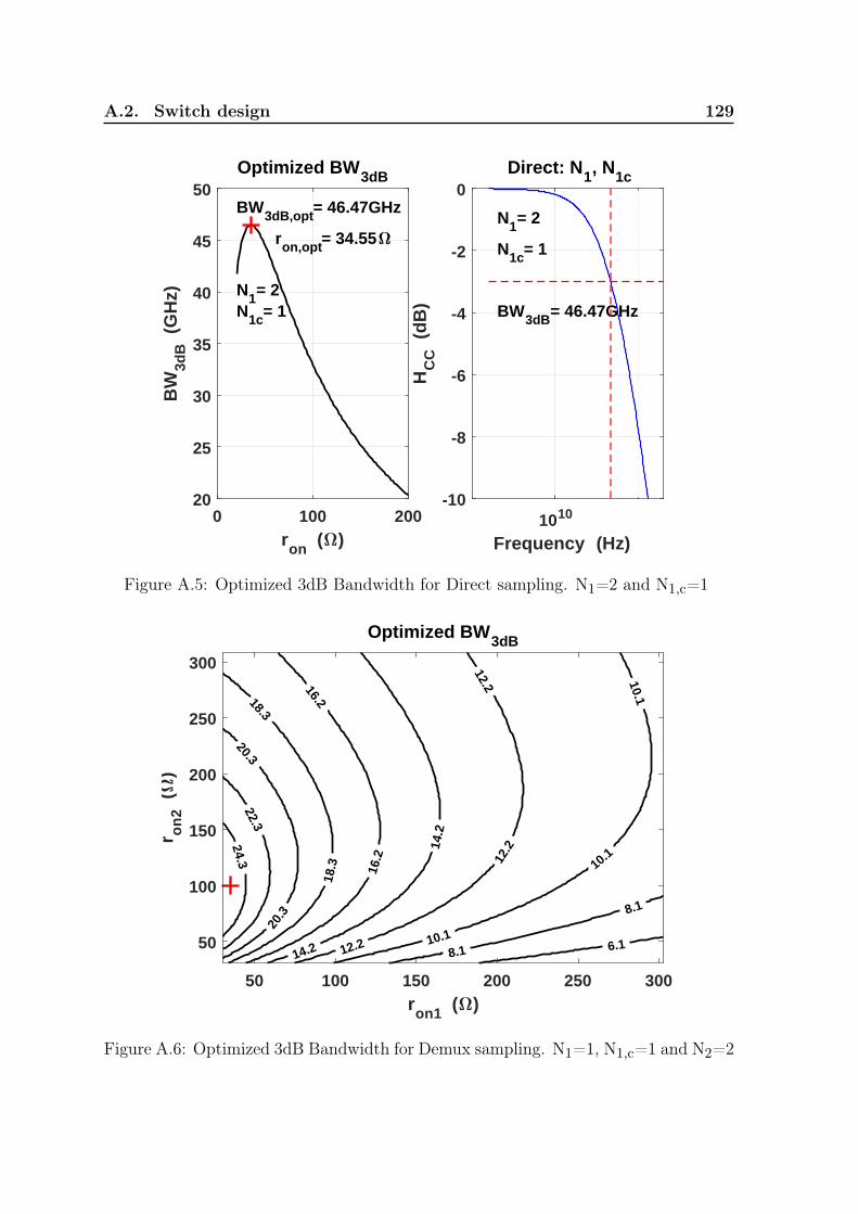
A.2. Switch design 129
0 100 200ron ( )
20
25
30
35
40
45
50B
W3d
B (
GH
z)Optimized BW3dB
N1= 2N1c= 1
BW3dB,opt= 46.47GHz
ron,opt= 34.55
1010
Frequency (Hz)
-10
-8
-6
-4
-2
0
HC
C (
dB
)
Direct: N1, N1c
N1= 2
N1c= 1
BW3dB= 46.47GHz
Figure A.5: Optimized 3dB Bandwidth for Direct sampling. N1=2 and N1,c=1
Optimized BW3dB
6.18.1
8.1
10.1
10.1
10.1
12.2
12.2
12.2
14.2
14.2
16.2
16.2
18.3
18.3
20.3
20.322.3
24.3
50 100 150 200 250 300ron1 ( )
50
100
150
200
250
300
r on
2 ()
Figure A.6: Optimized 3dB Bandwidth for Demux sampling. N1=1, N1,c=1 and N2=2

Appendix B
Back Gate Biasing CalibrationMethodology
An optimized calibration methodology for high-speed comparators is presented. The
key features of this methodology are the offset extraction technique and the back
gate biasing calibration. The offset extraction technique uses a fast and accurate
smart resettable successive approximation register (SR-SAR) algorithm to calculate
the offset voltage (VOS). The back gate biasing calibration is a simple iterative loop,
where the back gate bias of the comparator’s differential input pair is monotonically
increased or decreased to counter balance the extracted offset voltage at each iteration.
B.1 Comparator Test Bench
The proposed back gate biasing calibration methodology is implemented using the test
bench of Figure B.1. It consists of three blocks: the comparator, the back gate biasing
DAC and the VOS calibration control.
The control block is a Verilog-A model in charge of generating the inputs for the
comparator and resistor ladder, reading out the comparator’s output and adjusting the
back gate biasing DAC accordingly to the calculated offset. The calibration operates
in two phases: VOS extraction and VOS calibration. The extraction is a fast loop
operating at the comparator’s clock frequency ΦCLK and follows the smart resettable
SAR (SR-SAR) technique presented in [49]. Here, the voltage offset is calculated. The
second phase is a slow loop (below 1 MHz), due to the low frequency nature of the
transistor’s back gate. After extracting the VOS, the control block begins to change
the comparator’s back gate biasing until VOS ≈ 0 or a margin is reached.

B.1. Comparator Test Bench 131
−
+−+
Vin,p
Vinm Voutp
Voutm
ΦC
LK
Ladderenable
Ladder[5:0]
VOS,R
VOS,F
ΦCLK
Vin,p
Vin,M
VOSCalibration
Control
Ladenable
Ladcode[5:0]
VB
BP
VB
BN
Ladder
Resistive
Slow Loop : Ladder
Fast Loop : Offset
Figure B.1: Comparator testbench for back gate biasing calibration
B.1.1 Offset Extraction
The offset extraction technique SR-SAR in [49], is proposed as a fast and accurate
alternative to the conventional linear search technique, which is simple and accurate
but suffers from long simulation time. The SR-SAR uses a modified SAR algorithm
to determine the comparator offset voltage in a much shorter time. The input of
the comparator is modified to provide a quasi-monotonic stimulus. It allows a well
defined crossing from low-to-high and high-to-low transitions. It yields to an accurate
extraction of the rising offset (VOSR) and falling offset (VOSF) voltages.
Figure B.2 depicts the operation principle of the SR-SAR technique. Two search
cycles (rising and falling) are performed, one cycle starting at the minimum level of the
search range and the other at the maximum. In either cycle, the input goes to reset
state if the next SAR value dictates a threshold crossing in a direction opposite to the
one being tested. In this example, an ideal comparator with hysteresis was evaluated
showing that VOSR and VOSF can be accurately extracted.
The number of cycles for the linear, SAR and SR-SAR techniques are given by

132 Appendix B. Back Gate Biasing Calibration Methodology
Table B.1. NBIT is the number of bits employed in the binary search and NCLK,SAR
is the number of clock cycles using only SAR.
Figure B.2: Offset voltage extraction technique showing: input differential voltage(Vind), output differential voltage (Voutd) and offset voltage (VOS)
Table B.1: Calibration Clock Cycles
Linear SAR SR-SAR
SearchRangeSearchResolution · 2 2(NBIT + 1)
NCLK,SAR + (NBIT -1)3NBIT+1
B.1.2 Comparator
The evaluated comparator is the one described in subsection 3.5.4. The offset
introduced by the input differential pair will be compensated using our proposed
calibration technique. Offset voltage suppression is achieved by adjusting VTH in
the differential pair through forward back gate biasing, which is allowed in FDSOI
technology.

B.1. Comparator Test Bench 133
Figure B.3: Histogram Strong ARM VOSR (blue) and VOSF (red): CLK=875MHzand CLK=10MHz for 1000 uncalibrated MC runs
B.1.3 Back gate biasing DAC
The back gate biasing DAC consists of a resistor ladder controlled by a 5-bit digital
word. In order to choose the variation range of the ladder, we need to extract the VOS
range of the comparator. Using Monte-Carlo (MC) simulations from the schematic,
a VOS range (+/-3σ) of ≈ 45mV was obtained for the nominal clock frequency of
875MHz. Additionally, the VOS was extracted for a low frequency of 10MHz, as seen
in Figure B.3. The reason behind it, is to reduce even further the simulation time
during calibration. As can be seen, there is little contribution due to memory effect at
875MHz, allowing us to clock the comparator at a lower frequency without loosing too
much accuracy. Table B.2 summarizes the MC results. A search range of +/-50mV
with a resolution of 0.1mV was used.
The nominal voltage supply for the comparator is 0.8V, the same for the back gate
bias at nominal operation. Figure B.4 shows the back gate bias control. The ladder

134 Appendix B. Back Gate Biasing Calibration Methodology
Table B.2: Schematic VOSExtraction
Search range -50 to 50mV
Resolution 0.1mV (10 bits)
ΦCLK 875MHz 10MHz
Mean (VOS,R) 4.19μV -15.89μV
σ (VOS,R) 7.542mV 7.543mV
Mean (VOS,F) -9.46μV -15.79μV
σ (VOS,F) 7.544mV 7.543mV
was designed using a resolution of 5 bits, with the back gate voltage varying between
0.4V to 0.8V. An artificial offset voltage range of +/- 32mV (≈ 2.1mV steps) was
created. For example, if a negative VOS is extracted, the calibration controller will
only choose from the positive range to counterbalance the negative VOS generated by
the differential pair.
Figure B.4: Back gate biasing DAC: back gate bias and offset voltage
B.2. Simulation Results 135
B.1.4 Offset Calibration
VOS calibration for the comparator consists in two phases:
1. VOS extraction:
• It begins with initialization of the back gate biased DAC, ladder code=15
→ VBBP=VBBN=0.8V,
• After initialization VOSR and VOSF are extracted.
2. VOS calibration:
• VOSR and VOSF determine the iteration sequence for the ladder with
VOS,init=VOSR=VOSF,
• For VOS,init<0, the ladder adds a positive VOS,iter[code]>0, with the code
starting at 0. For VOS,init>0, the code starts at 16 (VOS,iter[code]<0),
• The back gate bias are switched to the current code value: VBBP[code],
VBBN[code] and VOS,iter[code] is extracted,
• The iteration sequence continues until VOS,iter[code]<tolerance, i.e. 1mV
or the code reachs its final value.
Figure B.5 shows the time diagram of the comparator’s VOS calibration sequence
for VOS,init<0. The code transitions has a time step of 2.5μs and the comparator is
clocked at 10MHz (T=100ns). By clocking the comparator at low frequency, the time
step of the transient simulation is coarse enough to allow a much faster convergence
solution.
B.2 Simulation Results
The stair-case input signal to detect the comparator’s output transitions is the
standard technique for comparator offset simulation. The drawback of this technique
is the fine voltage step to achieve adequate precision. This simulation requires a very
long simulation time for a single VOS extraction and must be repeated enough times

136 Appendix B. Back Gate Biasing Calibration Methodology
Figure B.5: Back gate biasing calibration procedure showing: input differential voltage(Vind), DAC ladder code, DAC back gate voltage and offset voltage (VOS)
to calculate the statistical distribution of VOS. Thus, the total simulation time can
take several hours or more.
To evaluate the proposed calibration methodology, MC Post-Layout Simulations
(PLS) were performed on the comparator using the same search range and resolution
forVOS extraction. Table B.3 shows results ofVOS for 100 MC runs for an uncalibrated
and calibrated comparator. It clearly stands out the VOS mean and standard deviation
reduction for the calibrated comparator. The VOS mean was almost zeroed and the
standard deviation was reduced by a factor of 12. Another aspect to point out is the
larger VOS of the uncalibrated version, but this did not present any issues since the
resistor ladder was designed with some margin.
The other important aspect of this methodology is the simulation time reduction.
Table B.4 presents the simulation time for the VOS extraction and calibration for the
schematic and post-layout views of the comparator. The time saving in the design
process can be seen. For a first design version (schematic) of the comparator, it can

B.2. Simulation Results 137
Table B.3: Post-Layout VOS Calibration.
Search range -50 to 50mV
Resolution 0.1mV (10 bits)
ΦCLK 10MHz
Uncalibrated Calibrated
Mean (VOS) -1.61mV 0.02mV
σ (VOS) 8.86mV 0.73mV
only take up to 40 minutes to estimate and calibrate the VOS and almost 4 hours to
validate the complete design with PLS results. The simulation time was reduced by a
factor of 64 compared to the linear calibration technique.
Table B.4: Simulation Time Summary
VOS Extraction (1000 MC runs) VOS Calibration (100 MC runs)
Schematic Post-Layout Schematic Post-Layout24min 1h50min 16min 1h56min

Bibliography
[1] M. Nowell. (2019) Cisco vni forecast update. [Online].
Available: https://www.ieee802.org/3/ad_hoc/bwa2/public/calls/19_0624/
nowell_bwa_01_190624.pdf (Cited on pages vii and 5.)
[2] B. Murmann. ADC Performance Survey 1997-2020. [Online]. Available: http:
//web.stanford.edu/~murmann/adcsurvey.html (Cited on pages ix, 54 and 91.)
[3] T. Shanley, InfiniBand Network Architecture. Mindshare Inc., 2002. (Cited on
page 5.)
[4] M. Wadekar, G. Hegde, N. Finn, H. Barrass, and J. Lynch. (2005) Proposal
for traffic differentiation in ethernet networks. [Online]. Available: https:
//www.ieee802.org/3/ar/public/0503/wadekar_1_0503.pdf (Cited on page 5.)
[5] Ethernet Alliance. The 2020 Ethernet Roadmap. [Online]. Available: https:
//ethernetalliance.org/technology/2020-roadmap/ (Cited on page 6.)
[6] IEEE P802.3ck, “100 Gb/s, 200 Gb/s, and 400 Gb/s Electrical Interfaces Task
Force,” 2019, http://www.ieee802.org/3/ck/. (Cited on pages 8 and 34.)
[7] M. Wu, “DesignCon 2017 112 Gbps Serial Transmission over Copper – PAM 4 vs
PAM 8 Signaling,” 2016. (Cited on pages 10 and 59.)
[8] M. N. Sakib and O. Liboiron-Ladouceur, “A study of error correction codes for
pam signals in data center applications,” IEEE Photonics Technology Letters,
vol. 25, no. 23, pp. 2274–2277, 2013. (Cited on page 12.)
[9] E. Sackinger, Analysis and Design of Transimpedance Amplifiers for Optical
Receivers. John Wiley & Sons, 2018. (Cited on page 12.)
[10] S. Palermo, “High-Speed Serial I/O Design for Channel-Limited and
Power-Constrained Systems,” in CMOS Nanoelectronics Analog and RF VLSI

Bibliography 139
Circuits, K. Iniewski, Ed. McGraw-Hill, 2011, ch. 9. (Cited on pages 13, 16, 20,
21 and 22.)
[11] C. Gimeno Gasca, S. Celma Pueyo, and C. Aldea Chagoyen, CMOS
Continuous-Time Adaptive Equalizers for High-Speed Serial Links. Springer
International Publishing, 2015. (Cited on pages 16, 19, 20 and 21.)
[12] J. D. Rockrohr, High Speed Serdes Devices and Applications. Boston, MA:
Springer US, 2009. (Cited on pages 20 and 21.)
[13] J. H. Winters and R. D. Gitlin, “Electrical signal processing techniques in
long-haul fiber-optic systems,” IEEE Transactions on Communications, vol. 38,
no. 9, pp. 1439–1453, 1990. (Cited on page 21.)
[14] K. Tan, P. Chiang, Y. Wang, H. Zhao, A. Roldan, H. Zhao, N. Narang, S. W. Lim,
D. Carey, S. L. Chaitanya Ambatipudi, P. Upadhyaya, Y. Frans, and K. Chang,
“A 112-Gb/s PAM4 Transmitter in 16nm FinFET,” in 2018 IEEE Symposium on
VLSI Circuits, 2018, pp. 45–46. (Cited on pages 23 and 24.)
[15] J. Kim, A. Balankutty, R. Dokania, A. Elshazly, H. S. Kim, S. Kundu, S. Weaver,
K. Yu, and F. O’Mahony, “A 112Gb/s PAM-4 transmitter with 3-Tap FFE in
10nm CMOS,” in 2018 IEEE International Solid - State Circuits Conference -
(ISSCC), 2018, pp. 102–104. (Cited on pages 23 and 24.)
[16] C. Menolfi, M. Braendli, P. A. Francese, T. Morf, A. Cevrero, M. Kossel, L. Kull,
D. Luu, I. Ozkaya, and T. Toifl, “A 112Gb/s 2.6pJ/b 8-Tap FFE PAM-4 SST TX
in 14nm CMOS,” in 2018 IEEE International Solid - State Circuits Conference -
(ISSCC), 2018, pp. 104–106. (Cited on pages 23 and 24.)
[17] Z. Toprak-Deniz, J. E. Proesel, J. F. Bulzacchelli, H. A. Ainspan, T. O. Dickson,
M. P. Beakes, and M. Meghelli, “6.6 A 128Gb/s 1.3pJ/b PAM-4 Transmitter with
Reconfigurable 3-Tap FFE in 14nm CMOS,” in 2019 IEEE International Solid-
State Circuits Conference - (ISSCC), 2019, pp. 122–124. (Cited on pages 23
and 24.)

140 Bibliography
[18] P. Peng, Y. Chen, S. Lai, C. Chen, H. Huang, and T. Shih, “6.7 A 112Gb/s
PAM-4 Voltage-Mode Transmitter with 4-Tap Two-Step FFE and Automatic
Phase Alignment Techniques in 40nm CMOS,” in 2019 IEEE International Solid-
State Circuits Conference - (ISSCC), 2019, pp. 124–126. (Cited on pages 23
and 24.)
[19] E. Groen, C. Boecker, M. Hossain, R. Vu, S. Vamvakos, H. Lin, S. Li, M. Van
Ierssel, P. Choudhary, N. Wang, M. Shibata, M. H. Taghavi, N. Nguyen, and
S. Desai, “6.3 A 10-to-112Gb/s DSP-DAC-Based Transmitter with 1.2Vppd
Output Swing in 7nm FinFET,” in 2020 IEEE International Solid- State Circuits
Conference - (ISSCC), 2020, pp. 120–122. (Cited on pages 23 and 24.)
[20] P. Peng, S. Lai, W. Wang, C. Lin, W. Huang, and T. Shih, “6.8 A 100Gb/s NRZ
Transmitter with 8-Tap FFE Using a 7b DAC in 40nm CMOS,” in 2020 IEEE
International Solid- State Circuits Conference - (ISSCC), 2020, pp. 130–132.
(Cited on pages 23 and 24.)
[21] E. Chen, R. Yousry, and C. K. Yang, “Power Optimized ADC-Based Serial Link
Receiver,” IEEE Journal of Solid-State Circuits, vol. 47, no. 4, pp. 938–951, 2012.
(Cited on page 24.)
[22] J. Hudner, D. Carey, R. Casey, K. Hearne, P. W. de Abreu Farias Neto,
I. Chlis, M. Erett, C. F. Poon, A. Laraba, H. Zhang, S. L. Chaitanya
Ambatipudi, D. Mahashin, P. Upadhyaya, Y. Frans, and K. Chang, “A 112GB/S
PAM4 Wireline Receiver Using a 64-Way Time-Interleaved SAR ADC in 16NM
FinFET,” in 2018 IEEE Symposium on VLSI Circuits, 2018, pp. 47–48. (Cited
on page 25.)
[23] Y. Krupnik, Y. Perelman, I. Levin, Y. Sanhedrai, R. Eitan, A. Khairi, Y. Landau,
U. Virobnik, N. Dolev, A. Meisler, and A. Cohen, “112 Gb/s PAM4 ADC Based
SERDES Receiver for Long-Reach Channels in 10nm Process,” in 2019 Symposium
on VLSI Circuits, 2019, pp. C266–C267. (Cited on page 25.)
Bibliography 141
[24] A. Cevrero, I. Ozkaya, P. A. Francese, M. Brandli, C. Menolfi, T. Morf, M. Kossel,
L. Kull, D. Luu, M. Dazzi, and T. Toifl, “6.1 A 100Gb/s 1.1pJ/b PAM-4 RX
with Dual-Mode 1-Tap PAM-4 / 3-Tap NRZ Speculative DFE in 14nm CMOS
FinFET,” in 2019 IEEE International Solid- State Circuits Conference - (ISSCC),
2019, pp. 112–114. (Cited on page 25.)
[25] C. Loi, A. Mellati, A. Tan, A. Farhoodfar, A. Tiruvur, B. Helal, B. Killips, F. Rad,
J. Riani, J. Pernillo, J. Sun, J. Wong, K. Abdelhalim, K. Gopalakrishnan, K. Kim,
L. Tse, M. Davoodi, M. Le, M. Zhang, M. Talegaonkar, P. Prabha, R. Mohanavelu,
S. Chong, S. Forey, S. Netto, S. Bhoja, W. Liew, Y. Duan, and Y. Liao, “6.5
A 400Gb/s Transceiver for PAM-4 Optical Direct-Detect Application in 16nm
FinFET,” in 2019 IEEE International Solid- State Circuits Conference - (ISSCC),
2019, pp. 120–122. (Cited on page 26.)
[26] J. Im, K. Zheng, A. Chou, L. Zhou, J. W. Kim, S. Chen, Y. Wang, H. Hung,
K. Tan, W. Lin, A. Roldan, D. Carey, I. Chlis, R. Casey, A. Bekele, Y. Cao,
D. Mahashin, H. Ahn, H. Zhang, Y. Frans, and K. Chang, “6.1 A 112Gb/s PAM-4
Long-Reach Wireline Transceiver Using a 36-Way Time-Interleaved SAR-ADC
and Inverter-Based RX Analog Front-End in 7nm FinFET,” in 2020 IEEE
International Solid- State Circuits Conference - (ISSCC), 2020, pp. 116–118.
(Cited on pages 26, 27 and 117.)
[27] T. Ali, E. Chen, H. Park, R. Yousry, Y. Ying, M. Abdullatif, M. Gandara, C. Liu,
P. Weng, H. Chen, M. Elbadry, Q. Nehal, K. Tsai, K. Tan, Y. Huang, C. Tsai,
Y. Chang, and Y. Tung, “6.2 A 460mW 112Gb/s DSP-Based Transceiver with
38dB Loss Compensation for Next-Generation Data Centers in 7nm FinFET
Technology,” in 2020 IEEE International Solid- State Circuits Conference -
(ISSCC), 2020, pp. 118–120. (Cited on pages 26 and 27.)
[28] W. C. Black and D. A. Hodges, “Time interleaved converter arrays,” IEEE Journal
of Solid-State Circuits, vol. 15, no. 6, pp. 1022–1029, 1980. (Cited on page 52.)

142 Bibliography
[29] R. H. Walden, “Analog-to-digital converter survey and analysis,” IEEE Journal
on Selected Areas in Communications, vol. 17, no. 4, pp. 539–550, 1999. (Cited
on page 54.)
[30] N. Kurosawa, H. Kobayashi, K. Maruyama, H. Sugawara, and K. Kobayashi,
“Explicit analysis of channel mismatch effects in time-interleaved ADC systems,”
IEEE Transactions on Circuits and Systems I: Fundamental Theory and
Applications, vol. 48, no. 3, pp. 261–271, 2001. (Cited on page 55.)
[31] B. Razavi, “Design considerations for interleaved adcs,” IEEE Journal of
Solid-State Circuits, vol. 48, no. 8, pp. 1806–1817, 2013. (Cited on pages 55
and 57.)
[32] M. Pelgrom, Quantization. Springer International Publishing, 2017, pp. 91–124.
(Cited on page 57.)
[33] D. Cordova, W. Cops, Y. Deval, F. Rivet, H. Lapuyade, N. Nodenot, and
Y. Piccin, “A Hierarchical Track and Hold Circuit for High Speed ADC-Based
Receivers in 22nm FDSOI,” in 2019 26th IEEE International Conference on
Electronics, Circuits and Systems (ICECS), 2019, pp. 358–361. (Cited on
page 59.)
[34] L. Kull, J. Pliva, T. Toifl, M. Schmatz, P. A. Francese, C. Menolfi, M. Brändli,
M. Kossel, T. Morf, T. M. Andersen, and Y. Leblebici, “Implementation of
Low-Power 6–8 b 30–90 GS/s Time-Interleaved ADCs with Optimized Input
Bandwidth in 32 nm CMOS,” IEEE Journal of Solid-State Circuits, vol. 51, no. 3,
pp. 636–648, 2016. (Cited on pages 61 and 78.)
[35] L. Kull, D. Luu, C. Menolfi, M. Brändli, P. A. Francese, T. Morf, M. Kossel,
A. Cevrero, I. Ozkaya, and T. Toifl, “A 24–72-GS/s 8-b Time-Interleaved SAR
ADCWith 2.0–3.3-pJ/Conversion and >30 dB SNDR at Nyquist in 14-nm CMOS
FinFET,” IEEE Journal of Solid-State Circuits, vol. 53, no. 12, pp. 3508–3516,
2018. (Cited on page 61.)
Bibliography 143
[36] Y. Duan and E. Alon, “A 12.8 GS/s Time-Interleaved ADCWith 25 GHz Effective
Resolution Bandwidth and 4.6 ENOB,” IEEE Journal of Solid-State Circuits,
vol. 49, no. 8, pp. 1725–1738, 2014. (Cited on pages 61 and 65.)
[37] S. Louwsma, E. van Tuijl, and B. Nauta, Time-interleaved Track and
Holds. Dordrecht: Springer Netherlands, 2011, pp. 5–38. [Online]. Available:
https://doi.org/10.1007/978-90-481-9716-3_2 (Cited on page 61.)
[38] K. Sun, G. Wang, Q. Zhang, S. Elahmadi, and P. Gui, “A 56-GS/s 8-bit
Time-Interleaved ADC With ENOB and BW enhancement Techniques in 28-nm
CMOS,” IEEE Journal of Solid-State Circuits, vol. 54, no. 3, pp. 821–833, March
2019. (Cited on page 68.)
[39] S. Kiran, S. Cai, Y. Luo, S. Hoyos, and S. Palermo, “A 52-Gb/s ADC-Based
PAM-4 Receiver With Comparator-Assisted 2-bit/stage SAR ADC and Partially
Unrolled DFE in 65-nm CMOS,” IEEE Journal of Solid-State Circuits, vol. 54,
no. 3, pp. 659–671, March 2019. (Cited on page 68.)
[40] J. Ramirez-Angulo, A. J. Lopez-Martin, R. G. Carvajal, A. Torralba, and
M. Jimenez, “Simple class-AB voltage follower with slew rate and bandwidth
enhancement and no extra static power or supply requirements,” Electronics
Letters, vol. 42, no. 14, pp. 784–785, 2006. (Cited on page 69.)
[41] W. Bae, “CMOS Inverter as Analog Circuit: An Overview,” Journal of Low Power
Electronics and Applications, vol. 9, no. 3, p. 26, Aug 2019. (Cited on page 75.)
[42] T. Rabuske and J. Fernandes, Review of SAR ADC Switching Schemes. Springer
International Publishing, 2017, pp. 25–67. (Cited on page 79.)
[43] B. P. Ginsburg and A. P. Chandrakasan, “Dual Time-Interleaved Successive
Approximation Register ADCs for an Ultra-Wideband Receiver,” IEEE Journal
of Solid-State Circuits, vol. 42, no. 2, pp. 247–257, 2007. (Cited on page 79.)

144 Bibliography
[44] C. Liu, S. Chang, G. Huang, and Y. Lin, “A 10-bit 50-MS/s SAR ADC With a
Monotonic Capacitor Switching Procedure,” IEEE Journal of Solid-State Circuits,
vol. 45, no. 4, pp. 731–740, April 2010. (Cited on page 81.)
[45] L. Deng, C. Yang, M. Zhao, Y. Liu, and X. Wu, “A 12-bit 200KS/s SAR ADC
with a Mixed Switching Scheme and Integer-Based Split Capacitor Array,” in 2013
IEEE 11th International New Circuits and Systems Conference (NEWCAS), June
2013, pp. 1–4. (Cited on page 82.)
[46] L. Kull, T. Toifl, M. Schmatz, P. A. Francese, C. Menolfi, M. Brändli,
M. Kossel, T. Morf, T. M. Andersen, and Y. Leblebici, “A 3.1 mW 8b 1.2
GS/s Single-Channel Asynchronous SAR ADC With Alternate Comparators for
Enhanced Speed in 32 nm Digital SOI CMOS,” IEEE Journal of Solid-State
Circuits, vol. 48, no. 12, pp. 3049–3058, Dec 2013. (Cited on pages 82 and 90.)
[47] Yan Zhu, U-Fat Chio, He-Gong Wei, Sai-Weng Sin, Seng-Pan U, and R. P.
Martins, “A power-efficient capacitor structure for high-speed charge recycling
SAR ADCs,” in 2008 15th IEEE International Conference on Electronics, Circuits
and Systems, 2008, pp. 642–645. (Cited on page 83.)
[48] H. Xu and A. A. Abidi, “Analysis and Design of Regenerative Comparators for
Low Offset and Noise,” IEEE Transactions on Circuits and Systems I: Regular
Papers, vol. 66, no. 8, pp. 2817–2830, Aug 2019. (Cited on page 84.)
[49] H. Omran, “Fast and accurate technique for comparator offset voltage simulation,”
Microelectronics Journal, vol. 89, pp. 91 – 97, 2019. (Cited on pages 85, 130
and 131.)
[50] R. Carter et al., “22nm FDSOI technology for emerging mobile,
Internet-of-Things, and RF applications,” in 2016 IEEE International Electron
Devices Meeting (IEDM), Dec 2016, pp. 2.2.1–2.2.4. (Cited on pages 87 and 124.)
[51] A. T. Ramkaj, M. Strackx, M. S. J. Steyaert, and F. Tavernier, “A 1.25-GS/s 7-b
SAR ADC With 36.4-dB SNDR at 5 GHz Using Switch-Bootstrapping, USPC
Bibliography 145
DAC and Triple-Tail Comparator in 28-nm CMOS,” IEEE Journal of Solid-State
Circuits, vol. 53, no. 7, pp. 1889–1901, July 2018. (Cited on page 90.)
[52] H. Wei, C. Chan, U. Chio, S. Sin, U. Seng-Pan, R. Martins, and F. Maloberti,
“A 0.024mm2 8b 400MS/s SAR ADC with 2b/cycle and resistive DAC in 65nm
CMOS,” in 2011 IEEE International Solid-State Circuits Conference, Feb 2011,
pp. 188–190. (Cited on page 90.)
[53] K. D. Choo, J. Bell, and M. P. Flynn, “27.3 Area-efficient 1GS/s 6b SAR ADC
with charge-injection-cell-based DAC,” in 2016 IEEE International Solid-State
Circuits Conference (ISSCC), Jan 2016, pp. 460–461. (Cited on page 90.)
[54] V. Saxena and R. J. Baker, “Indirect feedback compensation of CMOS op-amps,”
in 2006 IEEE Workshop on Microelectronics and Electron Devices, 2006. WMED
’06., 2006, pp. 2 pp.–4. (Cited on page 116.)
[55] B. Nauta, “A CMOS transconductance-C filter technique for very high
frequencies,” IEEE Journal of Solid-State Circuits, vol. 27, no. 2, pp. 142–153,
1992. (Cited on page 117.)
[56] K. Zheng, “System-driven circuit design for ADC-based wireline data links,” Ph.D.
dissertation, Stanford University, 2018. (Cited on page 117.)
[57] K. Zheng, Y. Frans, K. Chang, and B. Murmann, “A 56 Gb/s 6 mW 300 um2
inverter-based CTLE for short-reach PAM2 applications in 16 nm CMOS,” in
2018 IEEE Custom Integrated Circuits Conference (CICC), 2018, pp. 1–4. (Cited
on page 117.)
[58] P. G. A. Jespers and B. Murmann, Systematic Design of Analog CMOS
CircuitsUsing Pre-Computed Lookup Tables. Cambridge University Press, 2017.
(Cited on page 124.)