sthe technological institute - defense … institute i 1 contract now 62-0749-d memo no. 385 copy...
TRANSCRIPT

STHE
So TECHNOLOGICAL0• INSTITUTE
AERIALMEASUREMENTSLABORATORY
18i 1

TECHNOLOGICAL
INSTITUTE
I1
Contract NOw 62-0749-d Memo No. 385Copy No. /6s
SOL¶b1 STATE ANALOG-TO-DIGITAL CONVERTER
Fourth Quarterly Progress Report
February - March - April 1963
Paul G. Sedlewicz Robert E. Onley
I AERIAL
MEASUREMENTS
LABORATORY
I" NORTHWESTERN UNIVERSITY
1 Evanston, Illinois

iI
S1 CONTENTS
I Section Title Page
Ii Abstract ........................... ................... 1
I. Purpose ............................................... 2
j II. Discussion.
A. Introduction .................................... .. 3
B 1. Device tlandling ................................... 3
ITT. Investigation
A. Movement of Depletion Region ...................... 5
L . Cutoff Characteri.tic4 ............................ 21
IV. Summary and Results.................................... 31
V. Future Work ................................................ 32
I
IiI.

°1 -iii-
I ILLUSTRATIONS
I Figure Title Page
S1. Diffusion from a Concentration Step ............... 6
2. Acceptor and Donor Distributionof PN Wafer........................................ 9
3. Capacitance of Reverse Biased PN Wafer ............ 15
t 4. Movement of Depletion Layer on Bevel .............. 20
5. Forward and Reverse Characteristicsof Metal Probes ................................... 22
6. V-I Characteristics of tungsten Probeon Bevel .......................................... 25
7. Normalized Probe Current with IncreasingSDepletion Region .................................. 26
8. Normalized Probe Current with IncreasingChannel Depth ..................................... 27
9. Probe Cutoff Characteristics ...................... 30
Table Title Page
I I. Data on Diffusion( 6 ) .............. ............. ..... 7
II. Field and Potential Distributionsof ERFC Junction ................................... 13
II

I ABSTRACT
• lThis report presents equations for the movement of the
depletion region and for multiple probe cutoff. The movement
j of the depletion region along the bevel is related to an abrupt
junction movement times the amplification angle of the bevel.
An empirical equation relating the probe current to the reverse
1. bias of the PN bevel is given for the cutoff characteristics.
i
II
Ii
!111

j -2-
I,1l . Purpose
iIThe purpose of this contract is to conduct research and
development directed toward determining the feasibility of fabri-
I cating a solid-state analog-to-digital converter (or ADC). This
research is to be based on the movement of the depletion region
of a reverse biased PN crystal of silicon and the detection of
I this movement.
II_
IiIiI.I|

II. Discussion
• !A. Introduction
The cutoff characteristics of probes positioned on a beveled
IJ~ PN wafer and the movement of the depletion region are directly
related. The interaction of the probe current path (channel) with
I the depletion region causes the cutoff.
The original investigation( 1 )of the field and potential
distributions of our specific PN wafers was not adequate to develop
a theoretical cutoff equation. The movement of the depletion region
and the cutoff of the probes is complicated by the formation of the
Sjunction, beveling of the wafer, Current path. etc. During this
period the movenmnt and the cutoff were investigated for these
considerations and a theoretical model is presented.
j The cutoff of multiple probes can be investigated by using
a single probe. This single probe was used to obtain experimental
[i data on cutoff and. in conjunction with theoretical considerations.
an equation for the cutoff is presented. The limitations of this
equation. as to device configurations and characteristics were
1. considered and will be useful in describing device resolution.
The equation can be readily adapted to multiple probes, using basic
, parameters inherent within the device.
B. Device Handling
I Modification of an existing manipulator was carried
(1) lot Quarterly Progress Report, Solid State ADC, NOw 62-0749-d,Aerial Measurements Laboratory, Northwestern University,May-June-July, 1962.

out. This modification consisted of the introduction of a micro-
meter drive to the vertical movement of the adapted Wilder stage
and connection of terminals for the three leads from the wafer and
j probe. This change permits a more accurate positioning of the
probe on the beveled surface.
A dry box was obtained for test. It is a commercial plexi-
f glass box with a circulating system for passing the air through
desiccant tubes. The system works adequately and appears to pro-
duce a sufficiently dry atmosphere in which to work. Stages and
other equipment are presently being modified so that the position-
ing of multiple probes can be carried out conveniently in the dry
f. box.
I
Ii'

III. Investigation
I A. Movement of Depletion Region
The electrical properties of a reverse biased PN junction
are deduced directly from a solution of Poisson's equation in the
j space charge region. This equation is analytically integrable for
many charge distributions and a solution has been given for a
I diffused junction of the constant surface concentration type! 2 )
The type of charge distribution is presented and its application
to the one-dimensional solution of Poisson's equation is given.
J This derivation is then modified to represent the characteristic
of the beveled PN junction.
The formation of a P-type region within a single crystal of
N-type silicon by a diffusion process is represented by a solution
"of the diffusion equation! 3 )
F "--DVN (I)
DiThe diffusion coefficient D is the factor of proportionality relat-
•I ing the flow density F of diffusing atoms to the concentration
[gradient jN of the atoms.
The diffusion equation has been solved by Smits for the
constant surface concentration where only the initial conditions
have been considered.!(2) J. Cohen, Transition Region Properties of Reverse Biased
Diffused W4 Junt0ion, INT trans., ED-1 SeptemSer 1961,VIP 3=-3". i
(3) F.M. Suits, Foroation of Junction Structure by Solid StateI n i~ Proc. IRE Vol. 47, 115. 40, June IV"
1040-206
IIIO-0S

|~ x-
I
X 0
IWII
i Figure 1. Diffusion from a Concentration Step
S~The initial conditions can be specified by Figure 1.
•i N - 2No for X<O
]XI N- 0 for X>O
where No is the surface-concentration, constant for all time.
]i The diffusion from such initial conditions is described by
S~ the diffusion equation as:
0N•N erfc (X/2,AR) (2)
Thus the acceptor impurity distribution will be of the complementary
S~ error function type where
iir,,

I I--7
N a is the constant acceptor co centration0 at the surface (acceptor/cm)
X is the distance of diffusion from the
surface (cm)
ST is the time of diffusion (see)
f D is the diffusion constant of theacceptor (cma/sec)
erfc is the complementary error function(4)
I The diffusion constant (D), for silicon, has been worked out by
Fuller and Ditzenbergerf5)
The PN wafers used were of the constant surface concentration
type. Table I lists the diffusion data for these wafers.
Wafer Substrate P-type Dopant Surface Cone. (NO) Time 'rerqp.
B N type Si Boron 1020 atoms/em3 64 hrs 1260 0 C90*101 -cm
C N-type Si Boron 1018 atotls/cm3 4 irs 1264C
100o101i -cm -
Table I. Data on Diffusion( 6 "
(4) Table of the Error Function and its Derivative, U.F.Departmento - o" QrCe, I Mationa Bureau of Standards Applied with Series41, issued October 22, 1954,
(5) C. S. Fuller and J. A. Ditzenberger. Diffusion of Donor andI [ Acceptor Elements in Silicon, Journal •f pi-6P-lySicR,
Vol. 27, 1956, pp 544-553.
~ I(6) Thi wafers wore diffused by Htoffman Electronics Co.

II-
~ I Substituting values from Table I into Equation (2) a plot of the
j Iacceptor concentration can be obtained. Using the values for
wafer B, Equation (2) becomes;| 20
Na(X) = 10 erfc (X/21.4 x 10-4)
This equation is plotted in Figure 2 where the acceptor concentra-
tion as a function of distance from the surface is shown. Also
1. plotted in Figure 2 is the constant donor concentration Nd. The
donor concentration was obtained from the standard conductivity
equation (7), assuming all donors were ionized. This gives an Nd
of 5.3 x 10 donor atom- per cm 3 . The location of the junction
is obtained from the plot where
Nd - Na M 0
1 -3The location, 8.0 x 10 cm into the silicon, agrees within
I. experimental error with the location of the junction obtained by(8)
the preferential etching technique.
I. Solution of Poisson's equation for a .junction formed by constant
F surface concentration on a uniform concentration of donors has been
derived by Cohen.)
iI (7) R. D. Middleb~rook, An Introduction to Junction TransistorTheory, John Wiley and Sons, Inc., New York, 1957, Ch. 4I
(8) H. Bridges, J. Scoff, J. Shives, Transistor Technology,Vol. 1, 1958, Van Nostrand Co., N.Y.
I (9) See Reference (1)

I'�1I - -� F'
- - - - - - - - - - -- - - -- - - - - - -
- - - - - - - - - - -
I - - - -- - - - - --
- - - - -- - - - -
II
a.4
__ __ Vt
I Ii-- - - - -
a�III NF 0 IIIiI
II �aaI

I
~ I Poisson's Equation in this case is:
I~C P1+( x j[N erfc(-2) -N](3
where: E is the permittivity of silicon (f/cm)
j L 2,/•" is the diffusion length (cm)
Jl Transforming the equation so that it has a single parameter by the
following substitution:
SW •EV/q No L 2
N No /o
SEquation (3) reduces to:
d2W
ST erfc u-n (4)
where n - erfc uo aAd uo is the point of zero net charge. or the
junction.
j! The solutions of Equation (4) are in the form of second integrals
of the complementary error function and are difficult to manipulate,1)
but simple approximations can be made.
(10) L. Giacoletto, Junction Capacitance and Related Character-istics Using Graded Impurity Semiconductors, IRE, Trans.Vo [EDn-4, 1937. pp 207-215.

SI
I [ A graded junction is defined by (Nd - Na) - (a)(x-xo) where
(a) is a constant. Within the region of the junction a first order
Taylor expansion may be used.
I (Nd - Na) M[d(Nd -Na)/dXol (X-Xo) (5)
|. Shockley and others(n'12) have shown for a graded junction that
31-2q (Vv) (6)
I where
D - Il/(u2 - uI) is the normalized widthof the depletion region
V2 - VI is the potential dropacross the junction.I
The approximate field and potential distributions can now be
f obtained using Equations (4), (5). (6). The field distribution
becomes:
F a Fo + 1/2 (u - Uo) d erfc uo (7)
where F 4 EE/q NoL, the normalized field
F is the normalized field at u uo
F0(11) W, Shockley, The Theory of PN Junctions in Semiconductor
and PN Junction Transistors, Bell Systems Technical Journal,Vol. 28, 1949, pp 435-4Y9.
(12) D. Dewitt aad A. Roesoff, Transistor Electronics, WGraw-BillCom•any, N.Y., 1957, Ch. 2.
4;

I The potential distribution becomes:
I (W,-W 1) a d erfc uo/12D (8)
where d erfc u is the Gaussian function 2 exp (-u the
negative derivative of erfc u.
ii When the reverse potential across the diffused junction is
I" increased, it leaves the voltage region in which Equation (6) is
valid. Since Nd<<No the junction will enter the region where(13)
abrupt junction solution of Poisson's equation is valid. In the
abrupt region. the junction behaves very similarly to an infinite-
I step junction with a background doping of Nd. For such a junction,
Shockley( 14 ) has shown that:
2 L 4qq NdD 2# (V-VI) (9)
where the potential distribution is given as
(n 1 (10)
and the field distribution is given as
•I.F - Fo+n(U-uo) (11)
(17) L. B. Valdes, The Physical Theory of Transistors, McGraw-Hill Company, N.Y. 1961, Ch. 10
1 (14) goo Reference (11).
I
I

i I Thus Equations (7). (8), (10) and (11) characterize the potential
and field distributions of a diffused PN junction of the constant
surface concentration within the linear graded and abrupt regions.
I Table II gives these equations with the values resubstituted.
Graded Junction Region Abrupt Junction Region
Field qNo 2 qNdf Distribution E -E 0 +2-j(d erfc E -Eo÷ -- (xX-x)
(Potential qN0 X 3 X02"Distribution V - VI -i24-0 erfc )(XV-XI V2e1 -2- (Xa-X )
lITable II. Field and Potential Distributions of FRFC Junction
The voltage where the movement of the depletion region changes
from Equation (6) to Equation (9) is given by:
I. D (graded) - D (abrupt)
j and transition voltage Vc becomes2 318 q NL n21
ECd orfc u.0)
Substitution can be made into Equation (12) for the wafers used
and tabulated in Table I. Wafer B gives the transition voltage to
be
I Vc N 6.4 (volts)

Calculation on wafer C (Table I) gives a transition voltage of• VCA05 (volts)
j lThus, the potential distribution of the wafers over the major
portion of the depletion region is of the abrupt junction type and
the use of Equation (10) for the abrupt junction distribution is a
good approximation.
A capacitance versus reverse bias test was made on wafer C
and is shown in Figure 3. The transition from the initial slope
(for a linear graded junction movement) to the slope for an abrupt
junction movement occurs at approximately 7.5 volts. This shows
experimental verification of Equation (12) and further substantiates
the use of Equation (10) for the movement of the depletion layer
for the wafers.
The field and potential distributions of the constant surface
concentration diffusion within the depletion region can be approxi-
mated by the abrupt junction equation in the one-dimensional case.
This approximation can now be carried over to the beveled PN junction
where a two-dimensional field and potential distribution must be
considered.
The depletion reg6n of a beveled PN wafer is more complicated
than the one-dimensional case. The field and potential distri-
butions within the region of the bevel are now important and are
mathematically obtainable from a solution of Poisson's equation
in two dimensions. The discussion will be qualitative as to the
[ • field and potential distributions, using the laws of space charge
neutrality aad electrostatic tboory.

I I III
111
FIT
loo

°1i The depletion layer is maintained by the fixed ionized donors
and ionized acceptors on the N and P sides of the junction respec-
tively. This assumes a negligible number of mobile electrons and
holes within the depletion region. Since the donor and acceptor
concentrations are fixed throughout the crystal, a fixed field
[ and potential distribution must be established. This can be stated
as a space charge neutrality condition within the depletion region:
Na Vp - Nd Vn (13)
Equation (13) states that the total negative charge on the
P-side of the junction (ionized acceptor) must equal the total
positive charge on the N-side of the junction (ionized donor).
Beveling across the junction creates a larger volume on the P-side
f than on the N-side. This requires an increase in the depletion
region on the N-side close to the bevel, or a decrease on the
I P-side, or both. Gauss's Law can be stated so as to relate the
normal components of flux density along the bevel between the
depletion region and external media.(15)
Sd s.DS S -Di S=fiQ (14)S n n air (4
This equation states that the normal component of the flux density
I changes at the boundary by an amount equal to the surface charge
SI density. In the case where the surface charge density is zero,
(18) J. D. Kraus, Electromagnetics, McGraw-Hill Company, New York,193, Ch. I & 2.

I the normal components of D are equal. This requires the equi-
potential lines to meet the bevel surface perpendicularly, creat-
ing an increase in the depletion region on the N-side and a
I decrease on the P-side.
The ideal case (Q - 3. no surface states. etc.) would
I indicate an increase in the depletion region at the surface
greater than that predicted by the beveling of the PN junction.
Since the number of ionized donors at the surface is not zero,
Sand the number of surface states ( 1 6, 1 7 )can be substantial, the
increase will not be as great as predicted in the ideal case.
Through this qualitative argument it appears that the width of
the depletion region along the bevel will not be increased effec-
tively over that obtained by the amplification angle of the bevel.
This potential and field distribution of the beveled PN wafer
can now be related to the one-dimensional solutions discussed
I previously. Tt has been shown qualitatively that the decrease in
potential (or increase in movement) on the bevel can be related
to ,he ramp angle. This constant can be given as:
I (15)
(16) H. State, 0. DeMars, L. Davis, A. Adam, Surface States onSi and Ge Surfaces, Physical Review, Vol. 10, February
0 • 1959, pp 1272-1281.
(17) P. Handles, Electrical Properties of the Surface of Semi-|! conductors, The Surface Chemistry of Metals and Semiconductors,1. John Wiley and Sons. Inc,, New York, 1959, pp 54-71

where
SI is the angle of the bevel
f [The potential distribution along the bevel using Equation (10)
becomes:
2t2(V V (V2 - V (X 1 (16)
where
S(X2- XI) is the dimensional movement.
Equation (16) gives the potential distribution along the bevel as
a product of the abrupt junction potential distribution times the
geometric decrease due to the bevel. Assuming all the potential
is dropped across the junction:
( Iv - vI ) V Ra
and all the movement is into the N-material (since PpPn);
(X 2 - X1) - Xn
where Xn is the movement in the bulk.
Equation (16) can be rewritten as:
x (17a)
'I:U

and the width of the depletion region on the bevel is given by
2 (17b)
where X is the movement on the bevel (cm)
Equation (17b) has been verified experimentally by probing
for the depletion region with increasing reverse bias. Figure 4
J is the experimental curve and theoretical curve (Equation (17b)
for a B wafer with a bevel angle of 20 15'. The values obtained
from Table I are:
2 1 -35x10 (cm /volt)i
S1 256
The experimental curve is within experimental error of the
theoretical curve throughout the operating voltage range. Thus.
I the assumptions for the one dimensional solution of the erfc
junction and for the bevel region are within experimental tolerance.
1I
I

1 -20-
110
100
1 90
Iso
70
60
1 40
I 30
10
nw* a4W~ of 1~p*~sLw~Dvolt4m( 3e"r on O

1 -21-
I
B. Cutoff Characteristics
j The cutoff characteristics of the ADC can now be considered,
since equations for the movement were developed in the preceding
I section. The current path of the probe does not lend itself to
a rigorous mathematical solution, so an empirical approach will
Ii be used.
When a probe is positioned on the bevel and connected elec-
trically to the N-side, it can be characterized as a point contact
diode. The field through the N type silicon will be maximum along
the surface under the probe and decrease as a function of distance
below the probe. This distribution is complicated by the point
source appearance of the probe (probe appears as a point source
on an infinite sheet of silicon) and the coordinate positions of
the point contact with respect to the N-contact. The flow direc-
tion of current is not important in this analysis, but the current
density distribution below the probe, which interacts with the
movement of the depletion region, has an important relationship
to cutoff.
Contact to 4he high resistivity N-type material, by various
metal probes gave ohmic characteristics. The test of these probes
was made on a PN wafer which had its P-side lapped off. The
N-type surface was polished and etched in the same manner as the
beveled wafer, and the same pressure was applied to the probes as
for the beveled case. Figure 5 is a log-log plot of the V-I

-22-
I
10~ ~~~~~ w_____,- o~-
f 0' ' -1
. ...... .. .
A Ow
-i ..... Tu-...... -7I.... -- I-.-- -~-- -4 - -..-
I, , A
m 7 A-. " - -
3 4 ...... .. / .6 . to 5-4- 7 8o 3 I IA: I
S.... -H --.H -i
" -:--;--i, ---i:_ -_ • W- - - _ ••_,_,,•....'- -• _ .::."8- = '• .....- - - . ... .. _ • "
I .4 < ....
. - . , ,; , : i . _ -_ .I
Point Contact BiLas (volts)
Figure S. Forward and Reverse Characteritics~ of Iletal ]Probes

-23-
I
characteristics of various metal pressure contacts to the N-
substrate. The forward and reverse V-I characteristics of the
tungsten, zinc, and aluminuma probes are the same, and the slope
J in each case is approximately that of an ohmic contact. The!magnitude of the current calculated from Ohm's law was within
the right order of magnitude and the translation between the
three curves can be attiributed to the increase in contact area
for the various probes The gold probe appears to make rectifying
contact to the N-material where the forward current is shown to
be greater than the reverse current. This experiment was performed
immediately after the wafer was etched and several times within
the following few days with no change in any of the characteristics.
The tungsten probe has been used predominantly in testing.
The ohmic characteristics of the tungsten probe on the bevel can
be shown by plotting the forward and reverse resistances of the
contact as a function of distance down the wafer! 1 8 ) The resist-
ances are approximately equal.
An experiment was carried out to obtain an empirical equation
for the current density distribution below the probe. The tungsten
probe was placed at a floating potential of 80 volts, approximately
28 mils up the bevel from the junction. This position is well
above the junction, and should not influence the current path.
The V-I characteristics of the probe were taken with various
(18) 3rd Quarterly Progress Report, Solid State Analog-to-DigitalConverter, NOw 62-0749-d, Aerial Measurements Laboratory,Northwestern University, November-December 1962, January 1963.
I

-24-
!
reverse biases on the PN bevel and are plotted in Figure 6. This
technique, in effect. shows the decrease in probe current as the
depletion region moves toward the contact reducing the current
Schannel. Since the relationship between the reverse voltage (VR)
of the wafer and the movement of the depletion layer has been
previously determined, the various reverse voltages can be related
to decreases in the width of the channel below the probe.
Figure 7 is a plot of normalized probe current (at a constant
probe voltage) versus the width of the depletion region (along the
bevel and in the bulk). This is a plot taken from Figure 6 at a
constant voltage where the reverse voltage has been related to
movement by Equation (17a) of the last section. The width of the
channel below the probe as a function of normalized current density
can now be plotted since the position of the probe above the
junction is known. Figure 8 is a plot of channel depth versus
normalized probe current taken from Figure 7. This curve shows
the increase in current with increasing channel width. Al expo-
nential can be fitted to this curve where the best fit is:
I/Io 1 [1 - exponential -- (4.25 x 10 ) x'] (18)
where X is vertical distance below the probe in mils.
Equation (18) can be considered a general equation for the cutoff
characteristic by making a transformation of the origin from the
I

j -25-
j1001 2 3 4 67 9 4 5
7.,
1~ --
.3~ 3__ 8 ___1
'1. ,1 .
Prob VolagFigure~ ~ 6.V1Chrcersis1fT2:nPrb n ee

-26-
r4-
%0 N
__ __ ~~ '0
Pi v
'4~~~O M__
__ __
a%_ to_ %__ m e
Ov____ub ____rm ae~mo

-27-
p44
- _ _ A
N *
knomalue~o poi. 0(01/

-29-
I Equation (21) was obtained from empirical results and theo-
f. retical calculations. The current 10 must be calculated for
VR - 0 at each Vfo and the floating potential is given by the open
I circuit voltage of the particular probe. This equation gives a
good fit to the experimental results but only through further test
I can a best fit be obtained.
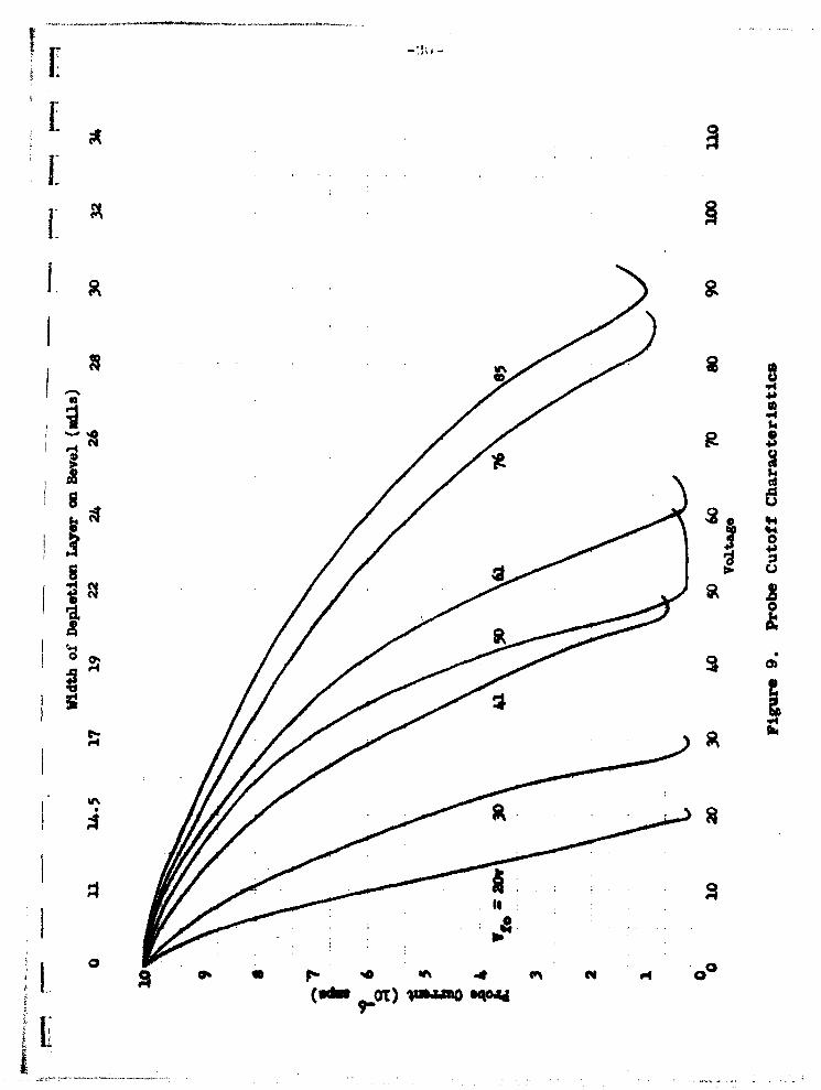
Figure 9 shows a series of cutoff characteristics obtained
with a single probe positioned at different floating potentials.
These curves are typical of a family of curves obtained from
multiple probes. There are discrepancies in these characteristics
which are not considered in the present derivation but which will
be compensated for through more experimental data.
I
I
L
r Ii -
Ii �iiIi �
2.
S1w .20
t�.
I'i g
44I
:1 (�
[k

I. IV. Summary and Results
[i The movement of the depletion region can be described by
the abrupt junction solution times the amplification angle for
j the beveled unit. The resistivity of the N-type silicon is
important in this solution and from all indications a more
I accurate check of resistivity is required. The abrupt junction
solution gives a good fit for these wafers but each new diffused
junction must be checked as to how well it follows the approxi-
mations used.
The cutoff characteristics can be described by the equations
given. These equations are empirical because of the nature of
the current path and through further studies a better fit can be
obtained. These equations will be useful in defining the reso-
lution of the device.
:1
i

ji, -32-
L V. Future Work
/ With the equipment presently being reworked, positioning of
multiple. probes will be carried out in the dry box. The posi-
tioning and attaching of probes to the beveled surface will be
attempted again but with more control of the ambient atmosphere
and the surface. Electrical characteristics of the multiple probe
cutoffs will be taken and compared to the cutoff equation presented
in this report.
I1.