step-up regulator and high-voltage step-up with ... · step-up regulator and high-voltage step-up...
TRANSCRIPT
_______________________________________________________________ Maxim Integrated Products 1
For pricing, delivery, and ordering information, please contact Maxim Direct at 1-888-629-4642, or visit Maxim’s website at www.maxim-ic.com.
Step-Up Regulator and High-Voltage Step-Up with Temperature Compensation
MA
X1
71
06
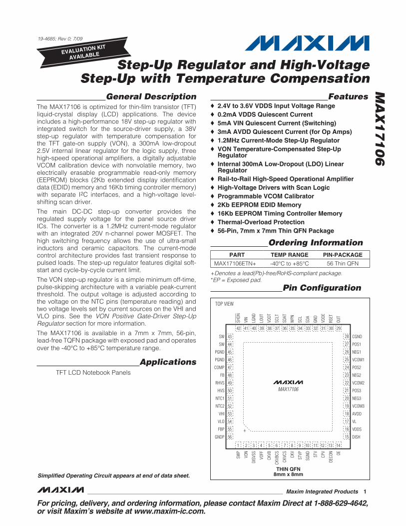
General DescriptionThe MAX17106 is optimized for thin-film transistor (TFT) liquid-crystal display (LCD) applications. The device includes a high-performance 18V step-up regulator with integrated switch for the source-driver supply, a 38V step-up regulator with temperature compensation for the TFT gate-on supply (VON), a 300mA low-dropout 2.5V internal linear regulator for the logic supply, three high-speed operational amplifiers, a digitally adjustable VCOM calibration device with nonvolatile memory, two electrically erasable programmable read-only memory (EEPROM) blocks (2Kb extended display identification data (EDID) memory and 16Kb timing controller memory) with separate I2C interfaces, and a high-voltage level-shifting scan driver.
The main DC-DC step-up converter provides the regulated supply voltage for the panel source driver ICs. The converter is a 1.2MHz current-mode regulator with an integrated 20V n-channel power MOSFET. The high switching frequency allows the use of ultra-small inductors and ceramic capacitors. The current-mode control architecture provides fast transient response to pulsed loads. The step-up regulator features digital soft-start and cycle-by-cycle current limit.
The VON step-up regulator is a simple minimum off-time, pulse-skipping architecture with a variable peak-current threshold. The output voltage is adjusted according to the voltage on the NTC pins (temperature reading) and two voltage levels set by current sources on the VHI and VLO pins. See the VON Positive Gate-Driver Step-Up Regulator section for more information.
The MAX17106 is available in a 7mm x 7mm, 56-pin, lead-free TQFN package with exposed pad and operates over the -40NC to +85NC temperature range.
ApplicationsTFT LCD Notebook Panels
FeaturesS 2.4V to 3.6V VDDS Input Voltage RangeS 0.2mA VDDS Quiescent CurrentS 5mA VIN Quiescent Current (Switching)S 3mA AVDD Quiescent Current (for Op Amps)S 1.2MHz Current-Mode Step-Up RegulatorS VON Temperature-Compensated Step-Up
RegulatorS Internal 300mA Low-Dropout (LDO) Linear
RegulatorS Rail-to-Rail High-Speed Operational AmplifierS High-Voltage Drivers with Scan LogicS Programmable VCOM CalibratorS 2Kb EEPROM EDID MemoryS 16Kb EEPROM Timing Controller MemoryS Thermal-Overload ProtectionS 56-Pin, 7mm x 7mm Thin QFN Package
19-4685; Rev 0; 7/09
Pin Configuration
Simplified Operating Circuit appears at end of data sheet.
Ordering Information
+Denotes a lead(Pb)-free/RoHS-compliant package.*EP = Exposed pad.
EVALUATION KIT
AVAILABLE
PART TEMP RANGE PIN-PACKAGE
MAX17106ETN+ -40NC to +85NC 56 Thin QFN
TOP VIEW
MAX17106
THIN QFN8mm x 8mm
15
17
16
18
19
20
21
22
23
24
25
26
27
28
DISH
VDDS
VL
AVDD
VCOM3
NEG3
POS3
VCOM2
NEG2
POS2
VCOM1
NEG1
POS1
CGND
GNDP
FBP
VLO
VHI
NTC2
NTC1
HVS
RHVS
FB
COMP
PGND
PGND
SW
SW
48
47
46
45
44
43
54
53
56
55
52
51
50
49
1 2 3 4 5 6 7 8 9 10 11 12 13 14
42 41 40 39 38 37 36 35 34 33 32 31 30 29CP
V
OECO
N OESTV
SGND
STVPCK
V
CKVC
S
CKVB
CS
CKVB
VOFF
DISV
SS
VON
SWP
VDDE
RSET
OUT
GND
SDA
SCL
WPN
SDAT
SCLT
VDDT
LOUT
LGND
VIN
SHDN
Step-Up Regulator and High-Voltage Step-Up with Temperature Compensation
MA
X1
71
06
2 ______________________________________________________________________________________
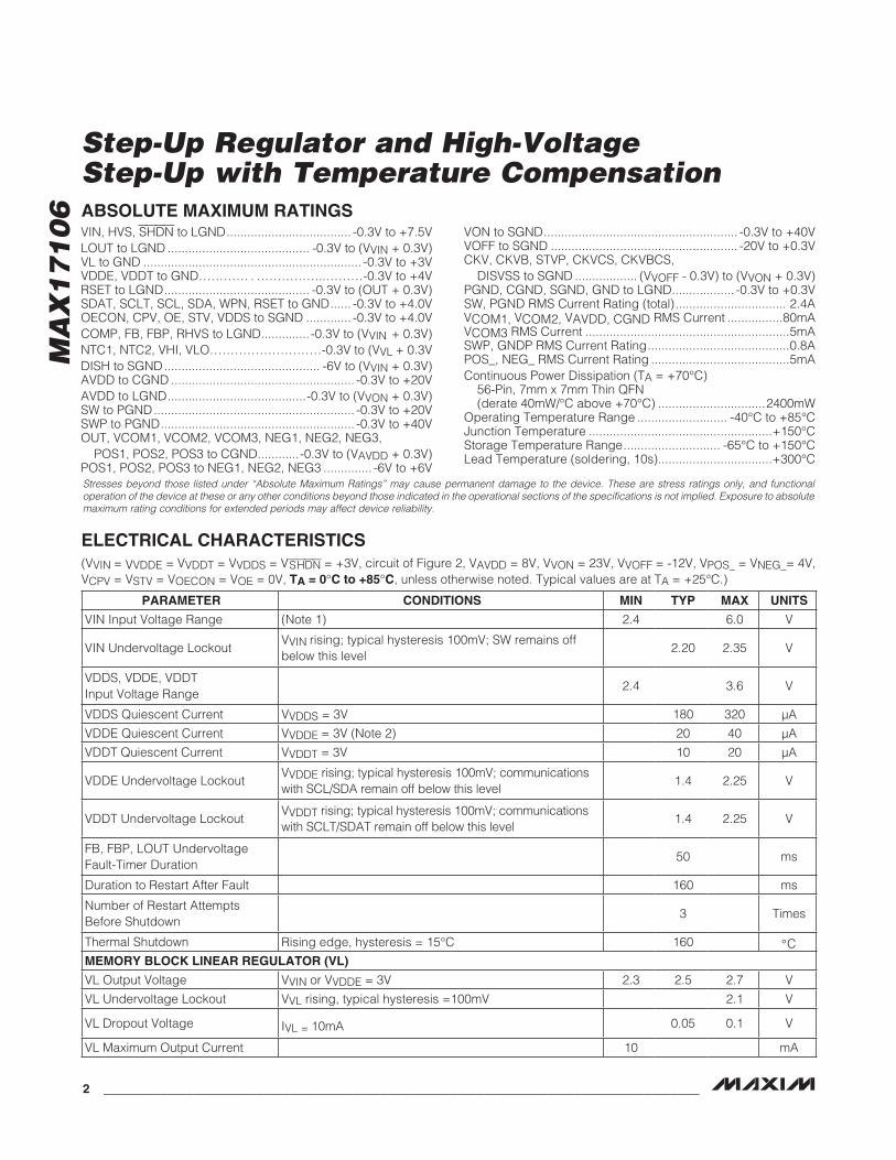
Stresses beyond those listed under “Absolute Maximum Ratings” may cause permanent damage to the device. These are stress ratings only, and functional operation of the device at these or any other conditions beyond those indicated in the operational sections of the specifications is not implied. Exposure to absolute maximum rating conditions for extended periods may affect device reliability.
VIN, HVS, SHDN to LGND .................................... -0.3V to +7.5VLOUT to LGND ......................................... -0.3V to (VVIN + 0.3V)VL to GND ............................................................... -0.3V to +3VVDDE, VDDT to GND………… . ……………..………-0.3V to +4VRSET to LGND .......................................... -0.3V to (OUT + 0.3V)SDAT, SCLT, SCL, SDA, WPN, RSET to GND ...... -0.3V to +4.0VOECON, CPV, OE, STV, VDDS to SGND ............. -0.3V to +4.0VCOMP, FB, FBP, RHVS to LGND .............. -0.3V to (VVIN + 0.3V)NTC1, NTC2, VHI, VLO………………………-0.3V to (VVL + 0.3VDISH to SGND ............................................. -6V to (VVIN + 0.3V)AVDD to CGND ..................................................... -0.3V to +20VAVDD to LGND ........................................-0.3V to (VVON + 0.3V)SW to PGND .......................................................... -0.3V to +20VSWP to PGND ........................................................ -0.3V to +40VOUT, VCOM1, VCOM2, VCOM3, NEG1, NEG2, NEG3,
POS1, POS2, POS3 to CGND ............-0.3V to (VAVDD + 0.3V)POS1, POS2, POS3 to NEG1, NEG2, NEG3 .............. -6V to +6V
VON to SGND ........................................................ -0.3V to +40VVOFF to SGND ...................................................... -20V to +0.3VCKV, CKVB, STVP, CKVCS, CKVBCS,
DISVSS to SGND .................. (VVOFF - 0.3V) to (VVON + 0.3V)PGND, CGND, SGND, GND to LGND .................. -0.3V to +0.3VSW, PGND RMS Current Rating (total) ................................ 2.4AVCOM1, VCOM2, VAVDD, CGND RMS Current ................80mAVCOM3 RMS Current ...........................................................5mASWP, GNDP RMS Current Rating .........................................0.8APOS_, NEG_ RMS Current Rating ........................................5mAContinuous Power Dissipation (TA = +70NC)
56-Pin, 7mm x 7mm Thin QFN (derate 40mW/NC above +70NC) ...............................2400mW
Operating Temperature Range .......................... -40NC to +85NCJunction Temperature .....................................................+150NCStorage Temperature Range ............................ -65NC to +150NCLead Temperature (soldering, 10s) .................................+300NC
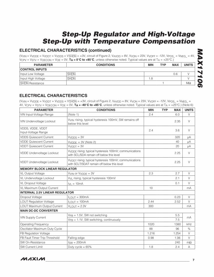
ELECTRICAL CHARACTERISTICS(VVIN = VVDDE = VVDDT = VVDDS = VSHDN = +3V, circuit of Figure 2, VAVDD = 8V, VVON = 23V, VVOFF = -12V, VPOS_ = VNEG_= 4V, VCPV = VSTV = VOECON = VOE = 0V, TA = 0NC to +85NC, unless otherwise noted. Typical values are at TA = +25NC.)
ABSOLUTE MAXIMUM RATINGS
PARAMETER CONDITIONS MIN TYP MAX UNITS
VIN Input Voltage Range (Note 1) 2.4 6.0 V
VIN Undervoltage LockoutVVIN rising; typical hysteresis 100mV; SW remains off below this level
2.20 2.35 V
VDDS, VDDE, VDDTInput Voltage Range
2.4 3.6 V
VDDS Quiescent Current VVDDS = 3V 180 320 FA
VDDE Quiescent Current VVDDE = 3V (Note 2) 20 40 FA
VDDT Quiescent Current VVDDT = 3V 10 20 FA
VDDE Undervoltage LockoutVVDDE rising; typical hysteresis 100mV; communications with SCL/SDA remain off below this level
1.4 2.25 V
VDDT Undervoltage LockoutVVDDT rising; typical hysteresis 100mV; communications with SCLT/SDAT remain off below this level
1.4 2.25 V
FB, FBP, LOUT Undervoltage Fault-Timer Duration
50 ms
Duration to Restart After Fault 160 ms
Number of Restart Attempts Before Shutdown
3 Times
Thermal Shutdown Rising edge, hysteresis = 15NC 160 °CMEMORY BLOCK LINEAR REGULATOR (VL)
VL Output Voltage VVIN or VVDDE = 3V 2.3 2.5 2.7 V
VL Undervoltage Lockout VVL rising, typical hysteresis =100mV 2.1 V
VL Dropout Voltage IVL = 10mA 0.05 0.1 V
VL Maximum Output Current 10 mA
Step-Up Regulator and High-Voltage Step-Up with Temperature Compensation
MA
X1
71
06
_______________________________________________________________________________________ 3
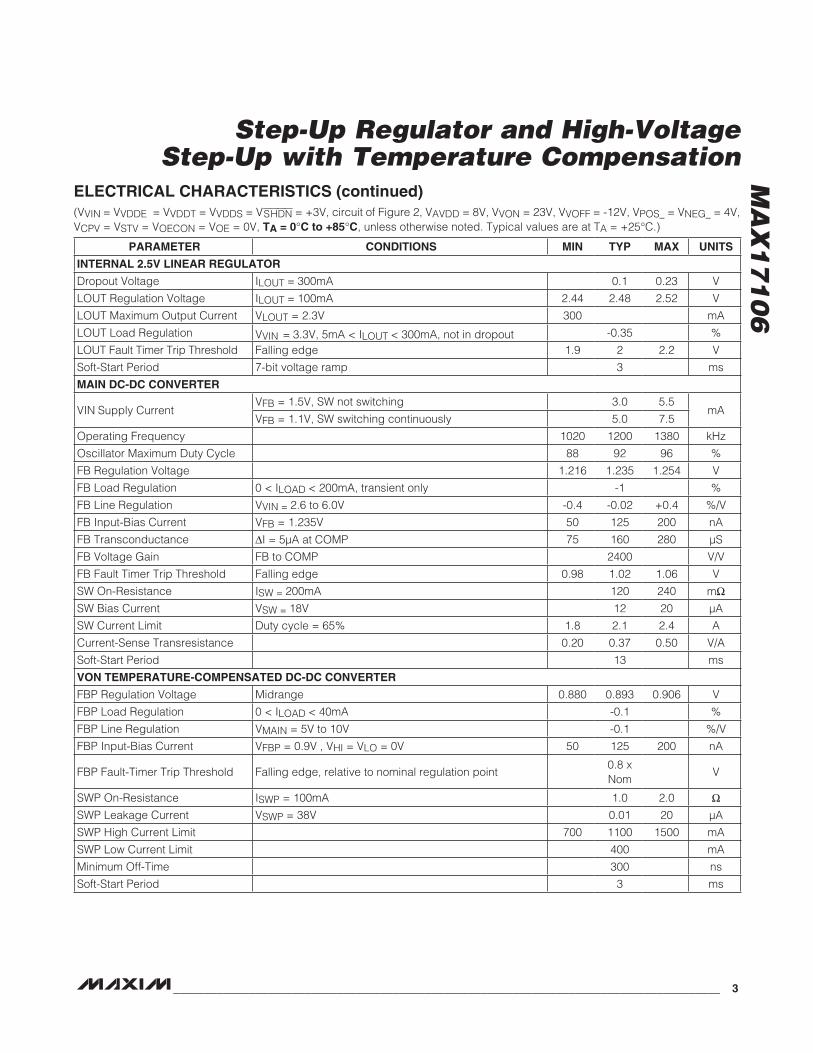
ELECTRICAL CHARACTERISTICS (continued)(VVIN = VVDDE = VVDDT = VVDDS = VSHDN = +3V, circuit of Figure 2, VAVDD = 8V, VVON = 23V, VVOFF = -12V, VPOS_ = VNEG_ = 4V, VCPV = VSTV = VOECON = VOE = 0V, TA = 0NC to +85NC, unless otherwise noted. Typical values are at TA = +25NC.)
PARAMETER CONDITIONS MIN TYP MAX UNITS
INTERNAL 2.5V LINEAR REGULATOR
Dropout Voltage ILOUT = 300mA 0.1 0.23 V
LOUT Regulation Voltage ILOUT = 100mA 2.44 2.48 2.52 V
LOUT Maximum Output Current VLOUT = 2.3V 300 mA
LOUT Load Regulation VVIN = 3.3V, 5mA < ILOUT < 300mA, not in dropout -0.35 %
LOUT Fault Timer Trip Threshold Falling edge 1.9 2 2.2 V
Soft-Start Period 7-bit voltage ramp 3 ms
MAIN DC-DC CONVERTER
VIN Supply CurrentVFB = 1.5V, SW not switching 3.0 5.5
mAVFB = 1.1V, SW switching continuously 5.0 7.5
Operating Frequency 1020 1200 1380 kHz
Oscillator Maximum Duty Cycle 88 92 96 %
FB Regulation Voltage 1.216 1.235 1.254 V
FB Load Regulation 0 < ILOAD < 200mA, transient only -1 %
FB Line Regulation VVIN = 2.6 to 6.0V -0.4 -0.02 +0.4 %/V
FB Input-Bias Current VFB = 1.235V 50 125 200 nA
FB Transconductance DI = 5FA at COMP 75 160 280 FS
FB Voltage Gain FB to COMP 2400 V/V
FB Fault Timer Trip Threshold Falling edge 0.98 1.02 1.06 V
SW On-Resistance ISW = 200mA 120 240 mI
SW Bias Current VSW = 18V 12 20 FA
SW Current Limit Duty cycle = 65% 1.8 2.1 2.4 A
Current-Sense Transresistance 0.20 0.37 0.50 V/A
Soft-Start Period 13 ms
VON TEMPERATURE-COMPENSATED DC-DC CONVERTER
FBP Regulation Voltage Midrange 0.880 0.893 0.906 V
FBP Load Regulation 0 < ILOAD < 40mA -0.1 %
FBP Line Regulation VMAIN = 5V to 10V -0.1 %/V
FBP Input-Bias Current VFBP = 0.9V , VHI = VLO = 0V 50 125 200 nA
FBP Fault-Timer Trip Threshold Falling edge, relative to nominal regulation point0.8 xNom
V
SWP On-Resistance ISWP = 100mA 1.0 2.0 I
SWP Leakage Current VSWP = 38V 0.01 20 FA
SWP High Current Limit 700 1100 1500 mA
SWP Low Current Limit 400 mA
Minimum Off-Time 300 ns
Soft-Start Period 3 ms
Step-Up Regulator and High-Voltage Step-Up with Temperature Compensation
MA
X1
71
06
4 ______________________________________________________________________________________
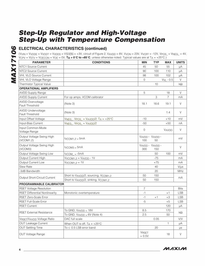
ELECTRICAL CHARACTERISTICS (continued)(VVIN = VVDDE = VVDDT = VVDDS = VSHDN = +3V, circuit of Figure 2, VAVDD = 8V, VVON = 23V, VVOFF = -12V, VPOS_ = VNEG_ = 4V, VCPV = VSTV = VOECON = VOE = 0V, TA = 0NC to +85NC, unless otherwise noted. Typical values are at TA = +25NC.)
PARAMETER CONDITIONS MIN TYP MAX UNITS
NTC1 Source Current 45 50 55 FA
NTC2 Source Current 90 100 110 FA
VHI, VLO Source Current 98 100 102 FA
VHI, VLO Voltage Range 0 VVL - 0.5 V
Thermistor Typical Value 10 kI
OPERATIONAL AMPLIFIERS
AVDD Supply Range 5 18 V
AVDD Supply Current For op amps, VCOM calibrator 3 7 mA
AVDD OvervoltageFault Threshold
(Note 3) 18.1 18.6 19.1 V
AVDD UndervoltageFault Threshold
(Note 3) 1.4 V
Input Offset Voltage VNEG_, VPOS_ = VAVDD/2, TA = +25NC -10 +10 mV
Input-Bias Current VNEG_, VPOS_ = VAVDD/2 -50 +50 nA
Input Common-ModeVoltage Range
0 VAVDD V
Output Voltage Swing High (VCOM1,2)
IVCOM1,2 = 5mAVAVDD -
100VAVDD -
50mV
Output Voltage Swing High (VCOM3)
IVCOM3 = 5mAVAVDD -
300VAVDD -
150V
Output Voltage Swing Low IVCOM_ = -5mA 50 100 mV
Output Current High VVCOM1,2 = VAVDD - 1V -75 mA
Output Current Low VVCOM1,2 = 1V +75 mA
Slew Rate 40 V/Fs
-3dB Bandwidth 20 MHz
Output Short-Circuit CurrentShort to VAVDD/2, sourcing, VCOM1,2 50 150
mAShort to VAVDD/2, sinking, VCOM1,2 50 150
PROGRAMMABLE CALIBRATOR
RSET Voltage Resolution 7 Bits
RSET Differential Nonlinearity Monotonic overtemperature -1 +1 LSB
RSET Zero-Scale Error -1 +1 +3 LSB
RSET Full-Scale Error -5 +5 LSB
RSET Current 120 FA
RSET External Resistance To GND, VAVDD = 18V 8.5 170
kITo GND, VAVDD = 6V (Note 4) 2.5 50
VRSET/VAVDD Voltage Ratio DAC full scale 0.05 V/V
OUT Leakage Current When OUT is off, TA = +25°C 1 FA
OUT Settling Time To P 0.5 LSB error band 20 Fs
OUT Voltage RangeVRSET+ 0.5V
18 V

Step-Up Regulator and High-Voltage Step-Up with Temperature Compensation
MA
X1
71
06
_______________________________________________________________________________________ 5
ELECTRICAL CHARACTERISTICS (continued)(VVIN = VVDDE = VVDDT = VVDDS = VSHDN = +3V, circuit of Figure 2, VAVDD = 8V, VVON = 23V, VVOFF = -12V, VPOS_ = VNEG_ = 4V, VCPV = VSTV = VOECON = VOE = 0V, TA = 0NC to +85NC, unless otherwise noted. Typical values are at TA = +25NC.)
PARAMETER CONDITIONS MIN TYP MAX UNITS
MEMORY BLOCKS
EEPROM Write Cycles (Note 5) 1000 Cycles
2Kb EDID EEPROM First-Byte Write Time
00xh location, 1-byte or 8-byte write 55 ms
2Kb EDID EEPROM Subsequent Write Time
All other locations 0.5 ms
16Kb TCON EEPROM PageInitial Byte Write Time
000xh or 200xh or 400xh or 600xh location 55 ms
16Kb TCON EEPROM Page Subsequent Write Time
All other locations 0.8 ms
Programmable Calibrator Nonvolatile Write Time
Data byte 8’bxxxxxxx0 55 ms
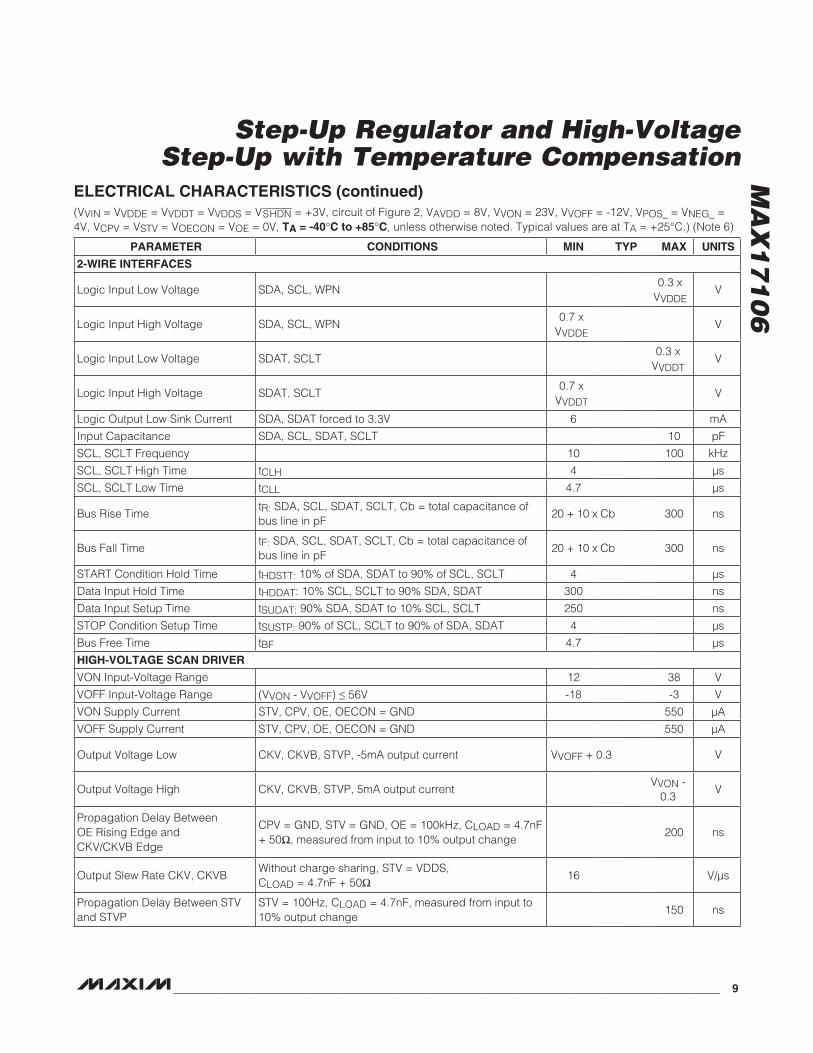
2-WIRE INTERFACES
Logic Input Low Voltage SDA, SCL, WPN0.3 x
VVDDEV
Logic Input High Voltage SDA, SCL, WPN0.7 x
VVDDEV
Logic Input Low Voltage SDAT, SCLT 0.3 x
VVDDTV
Logic Input High Voltage SDAT, SCLT 0.7 x
VVDDTV
Logic Output Low Sink Current SDA, SDAT forced to 3.3V 6 mA
Logic Input Current SDA, SCL, SDAT, SCLT to VIN or GND, TA = +25°C -1 +1 FA
WPN Input Current VWPN = 3.3V 14 35 FA
Input Capacitance SDA, SCL, SDAT, SCLT 5 10 pF
SCL, SCLT Frequency 10 100 kHz
SCL, SCLT High Time tCLH 4 Fs
SCL, SCLT Low Time tCLL 4.7 Fs
Bus Rise TimetR: SDA, SCL, SDAT, SCLT , Cb = total capacitance of bus line in pF
20 + 10 x Cb
300 ns
Bus Fall TimetF: SDA, SCL, SDAT, SCLT , Cb = total capacitance of bus line in pF
20 + 10 x Cb
300 ns
START Condition Hold Time tHDSTT: 10% of SDA, SDAT to 90% of SCL, SCLT 4 Fs
Data Input Hold Time tHDDAT: 10% SCL, SCLT to 90% SDA, SDAT 300 ns
Data Input Setup Time tSUDAT: 90% SDA, SDAT to 10% SCL, SCLT 250 ns
STOP Condition Setup Time tSUSTP: 90% of SCL, SCLT to 90% of SDA, SDAT 4 Fs
Bus Free Time tBF 4.7 Fs

Step-Up Regulator and High-Voltage Step-Up with Temperature Compensation
MA
X1
71
06
6 ______________________________________________________________________________________
ELECTRICAL CHARACTERISTICS (continued)(VVIN = VVDDE = VVDDT = VVDDS = VSHDN = +3V, circuit of Figure 2, VAVDD = 8V, VVON = 23V, VVOFF = -12V, VPOS_ = VNEG_ = 4V, VCPV = VSTV = VOECON = VOE = 0V, TA = 0NC to +85NC, unless otherwise noted. Typical values are at TA = +25NC.)
PARAMETER CONDITIONS MIN TYP MAX UNITS
Input Filter Spike Suppression SDA, SCL, SDAT, SCLT, not tested 700 ns
HIGH-VOLTAGE SCAN DRIVER
VON Input Voltage Range 12 38 V
VOFF Input Voltage Range (VON - VOFF) ≤ 56V -18 -3 V
VON Supply Current STV, CPV, OE, OECON = GND 300 550 FA
VOFF Supply Current STV, CPV, OE, OECON = GND 350 550 FA
Output Voltage Low CKV, CKVB, STVP, -5mA output currentVVOFF + 0.3
VVOFF + 0.1
V
Output Voltage High CKV, CKVB, STVP, 5mA output currentVVON- 0.1
VVON - 0.3
V
Propagation Delay BetweenOE Rising Edge andCKV/CKVB Edge
CPV = GND, STV = GND, OE = 100kHz, CLOAD = 4.7nF + 50I, measured from input to 10% output change
100 200 ns
Output Slew Rate CKV, CKVBWithout charge sharing, STV = VDDS,CLOAD = 4.7nF + 50I
16 25 V/Fs
Propagation Delay Between STV and STVP
STV = 100Hz, CLOAD = 4.7nF, measured from input to 10% output change
50 150 ns
Output Slew Rate STVP CLOAD = 4.7nF + 50I, R1 = R2 = 200I 18 30 V/Fs
Charge-Sharing Switch Resistance
CKV to CKVCS and CKVB to CKVBCS 50 100 I
DISH Turn-On Threshold -1 -0.6 V
DISH Switch ResistanceVOFF = -3V VDISH = -3V 500 I
VOFF to GND, DISH = VIN 1 MI
DISVSS Switch ResistanceDISVSS to VON, switch on 10 20 I
DISVSS to VON, switch off 0.1 MI
STV, CPV, OE, OECON Input Current
STV = VDDS or GND; CPV = VDDS or GND;OE = VDDS or GND; OECON = VDDS or GND; TA = +25°C
-1 +1 FA
STV, CPV, OE Input Low Voltage 0.7 V
STV, CPV, OE Input High Voltage 1.8 V
OECON Input Threshold(Rising Edge)
0.5 x VVDDS
0.58 x VVDDS
0.66 x VVDDS
OECON Sink Current OECON = STV = VDDS 0.4 0.8 mA
CKV, CKVB, CKVCS, CKVBCS, STVP Output Three-State Current
CKV, CKVB, STVP, CKVCS, CKVBCS at midrail, three-state, TA = +25°C
-1 +1 FA
HVS FUNCTION
HVS Input Low Voltage 0.8 V
HVS Input High Voltage 1.8 V
HVS Input Pulldown Resistance 5 25 50 kI
RHVS Output Switch Current VHVS = 3V, VRHVS = 0.4V 20 mA
Step-Up Regulator and High-Voltage Step-Up with Temperature Compensation
MA
X1
71
06
_______________________________________________________________________________________ 7
ELECTRICAL CHARACTERISTICS(VVIN = VVDDE = VVDDT = VVDDS = VSHDN = +3V, circuit of Figure 2, VAVDD = 8V, VVON = 23V, VVOFF = -12V, VPOS_ = VNEG_ = 4V, VCPV = VSTV = VOECON = VOE = 0V, TA = -40NC to +85NC, unless otherwise noted. Typical values are at TA = +25NC.) (Note 6)
ELECTRICAL CHARACTERISTICS (continued)(VVIN = VVDDE = VVDDT = VVDDS = VSHDN = +3V, circuit of Figure 2, VAVDD = 8V, VVON = 23V, VVOFF = -12V, VPOS_ = VNEG_ = 4V, VCPV = VSTV = VOECON = VOE = 0V, TA = 0NC to +85NC, unless otherwise noted. Typical values are at TA = +25NC.)
PARAMETER CONDITIONS MIN TYP MAX UNITS
VIN Input-Voltage Range (Note 1) 2.4 6.0 V
VIN Undervoltage Lockout VVIN rising, typical hysteresis 100mV, SW remains off below this level
2.35 V
VDDS, VDDE, VDDTInput-Voltage Range
2.4 3.6 V
VDDS Quiescent Current VVDDS = 3V 320 FA
VDDE Quiescent Current VVDDE = 3V (Note 2) 40 FA
VDDT Quiescent Current VVDDT = 3V 20 FA
VDDE Undervoltage LockoutVVDDE rising; typical hysteresis 100mV; communications with SCL/SDA remain off below this level
2.25 V
VDDT Undervoltage LockoutVVDDT rising; typical hysteresis 100mV; communications with SCLT/SDAT remain off below this level
2.25 V
MEMORY BLOCK LINEAR REGULATOR
VL Output Voltage VVIN or VVDDE = 3V 2.3 2.7 V
VL Undervoltage Lockout VVL rising, typical hysteresis 100mV 2.1 V
VL Dropout Voltage IVL = 10mA 0.1 V
VL Maximum Output Current 10 mA
INTERNAL 2.5V LINEAR REGULATOR
Dropout Voltage ILOUT = 300mA 0.23 V
LOUT Regulation Voltage ILOUT = 100mA 2.44 2.52 V
LOUT Maximum Output Current VLOUT = 2.3V 300 mA
MAIN DC-DC CONVERTER
VIN Supply CurrentVFB = 1.5V, SW not switching 5.5
mAVFB = 1.1V, SW switching, continuously 7.5
Operating Frequency 1020 1380 kHz
Oscillator Maximum Duty Cycle 88 96 %
FB Regulation Voltage 1.216 1.254 V
FB Fault Timer Trip Threshold Falling edge 0.98 1.06 V
SW On-Resistance ISW = 200mA 240 mI
SW Current Limit Duty cycle = 65% 1.8 2.4 A
PARAMETER CONDITIONS MIN TYP MAX UNITS
CONTROL INPUTS
Input Low Voltage SHDN 0.6 V
Input High Voltage SHDN 1.8 V
SHDN Resistance 1 MI

Step-Up Regulator and High-Voltage Step-Up with Temperature Compensation
MA
X1
71
06
8 ______________________________________________________________________________________
ELECTRICAL CHARACTERISTICS (continued)(VVIN = VVDDE = VVDDT = VVDDS = VSHDN = +3V, circuit of Figure 2, VAVDD = 8V, VVON = 23V, VVOFF = -12V, VPOS_ = VNEG_ = 4V, VCPV = VSTV = VOECON = VOE = 0V, TA =-40NC to +85NC, unless otherwise noted. Typical values are at TA = +25NC.) (Note 6)
PARAMETER CONDITIONS MIN TYP MAX UNITS
VON TEMPERATURE-COMPENSATED DC-DC CONVERTER
FBP Regulation Voltage Midrange 0.880 0.906 V
SWP On-Resistance ISWP = 100mA 2.0 I
SWP High Current Limit 700 1500 mA
OPERATIONAL AMPLIFIERS
AVDD Supply Range 5 18 V
AVDD Supply Current For op amps, VCOM calibrator 8 mA
AVDD Overvoltage Fault Threshold (Note 3) 18.1 19.9 V
AVDD Undervoltage Fault Threshold
(Note 3) 1.4 V
Input Common-ModeVoltage Range
0 VAVDD V
PROGRAMMABLE CALIBRATOR
RSET Voltage Resolution 7 Bits
RSET Differential Nonlinearity Monotonic overtemperature -1 +1 LSB
RSET Zero-Scale Error -1 +3 LSB
RSET Full-Scale Error -5 +5 LSB
RSET Current 120 FA
RSET External Resistance(Note 4)
To GND, VAVDD = 18V 8.5 170kI
To GND, VAVDD = 6V 2.5 50
OUT Voltage RangeVRSET +
0.5V18 V
MEMORY BLOCKS
EEPROM Write Cycles (Note 5) 1000 Cycles
2Kb EDID EEPROM First Byte Write Time
00xh location, 1 byte or 8 byte write 58 ms
2Kb EDID EEPROM Subsequent Write Time
All other locations 0.5 ms
16Kb TCON EEPROM Page Initial Byte Write Time
000xh or 200xh or 400xh or 600xh location 58 ms
16Kb TCON EEPROM Page Subsequent Write Time
All other locations 0.8 ms
Programmable Calibrator Nonvolatile Write Time
Data byte 8’bxxxxxxx0 58 ms
Step-Up Regulator and High-Voltage Step-Up with Temperature Compensation
MA
X1
71
06
_______________________________________________________________________________________ 9
ELECTRICAL CHARACTERISTICS (continued)(VVIN = VVDDE = VVDDT = VVDDS = VSHDN = +3V, circuit of Figure 2, VAVDD = 8V, VVON = 23V, VVOFF = -12V, VPOS_ = VNEG_ = 4V, VCPV = VSTV = VOECON = VOE = 0V, TA = -40NC to +85NC, unless otherwise noted. Typical values are at TA = +25NC.) (Note 6)
PARAMETER CONDITIONS MIN TYP MAX UNITS
2-WIRE INTERFACES
Logic Input Low Voltage SDA, SCL, WPN0.3 x
VVDDEV
Logic Input High Voltage SDA, SCL, WPN0.7 x
VVDDEV
Logic Input Low Voltage SDAT, SCLT 0.3 x
VVDDTV
Logic Input High Voltage SDAT, SCLT 0.7 x
VVDDTV
Logic Output Low Sink Current SDA, SDAT forced to 3.3V 6 mA
Input Capacitance SDA, SCL, SDAT, SCLT 10 pF
SCL, SCLT Frequency 10 100 kHz
SCL, SCLT High Time tCLH 4 Fs
SCL, SCLT Low Time tCLL 4.7 Fs
Bus Rise TimetR: SDA, SCL, SDAT, SCLT, Cb = total capacitance of bus line in pF
20 + 10 x Cb 300 ns
Bus Fall TimetF: SDA, SCL, SDAT, SCLT, Cb = total capacitance of bus line in pF
20 + 10 x Cb 300 ns
START Condition Hold Time tHDSTT: 10% of SDA, SDAT to 90% of SCL, SCLT 4 Fs
Data Input Hold Time tHDDAT: 10% SCL, SCLT to 90% SDA, SDAT 300 ns
Data Input Setup Time tSUDAT: 90% SDA, SDAT to 10% SCL, SCLT 250 ns
STOP Condition Setup Time tSUSTP: 90% of SCL, SCLT to 90% of SDA, SDAT 4 Fs
Bus Free Time tBF 4.7 Fs
HIGH-VOLTAGE SCAN DRIVER
VON Input-Voltage Range 12 38 V
VOFF Input-Voltage Range (VVON - VVOFF) P 56V -18 -3 V
VON Supply Current STV, CPV, OE, OECON = GND 550 FA
VOFF Supply Current STV, CPV, OE, OECON = GND 550 FA
Output Voltage Low CKV, CKVB, STVP, -5mA output current VVOFF + 0.3 V
Output Voltage High CKV, CKVB, STVP, 5mA output currentVVON -
0.3V
Propagation Delay BetweenOE Rising Edge andCKV/CKVB Edge
CPV = GND, STV = GND, OE = 100kHz, CLOAD = 4.7nF + 50I, measured from input to 10% output change
200 ns
Output Slew Rate CKV, CKVBWithout charge sharing, STV = VDDS,CLOAD = 4.7nF + 50I
16 V/Fs
Propagation Delay Between STV and STVP
STV = 100Hz, CLOAD = 4.7nF, measured from input to 10% output change
150 ns

Step-Up Regulator and High-Voltage Step-Up with Temperature Compensation
MA
X1
71
06
10 _____________________________________________________________________________________
ELECTRICAL CHARACTERISTICS (continued)(VVIN = VVDDE = VVDDT = VVDDS = VSHDN = +3V, circuit of Figure 2, VAVDD = 8V, VVON = 23V, VVOFF = -12V, VPOS_ = VNEG_ = 4V, VCPV = VSTV = VOECON = VOE = 0V, TA = -40NC to +85NC, unless otherwise noted. Typical values are at TA = +25NC.) (Note 6)
Note 1: For 5.5V < VVIN < 6.0V, use IC for no longer than 1% of IC lifetime. For continuous operation, input voltage should not exceed 5.5V.
Note 2: If VVDDE > VVIN, the VVDDE quiescent current increases to a max of 2mA.Note 3: SW switching is not enabled until AVDD is above undervoltage threshold and below the overvoltage threshold.Note 4: RSET external resistor range is verified at DAC full scale.Note 5: Guaranteed by design, not production tested.Note 6: TA = -40NC specs are guaranteed by design, not production tested.
Figure 1. Timing Definitions Used in the Electrical Characteristics
SCLSCLT
tHDSTT
tHDDAT tSUDAT tSUSTPtBF
tCLL
tCLH
tR
tF
VIH
VIL
SDASDAT
PARAMETER CONDITIONS MIN TYP MAX UNITS
Output Slew Rate STVP CLOAD = 4.7nF + 50I, R1 = R2 = 200I 18 V/Fs
Charge-Sharing Switch Resistance CKV to CKVCS and CKVB to CKVBCS 100 I
DISH Turn-On Threshold -1 V
DISH Switch ResistanceVOFF = -3V VDISH = -3V 500 I
VOFF to GND, DISH = VIN 1 MI
DISVSS Switch ResistanceDISVSS to VON, switch on 20 I
DISVSS to VON, switch off 0.1 MI
STV, CPV, OE Input Low Voltage 0.7 V
STV, CPV, OE Input High Voltage 1.8 V
HVS FUNCTION
HVS Input Low Voltage 0.8 V
HVS Input High Voltage 1.8 V
HVS Input Pulldown Resistance 5 50 kI
CONTROL INPUTS
Input Low Voltage SHDN 0.6 V
Input High Voltage SHDN 1.8 V
SHDN Resistance MI
Step-Up Regulator and High-Voltage Step-Up with Temperature Compensation
MA
X1
71
06
______________________________________________________________________________________ 11
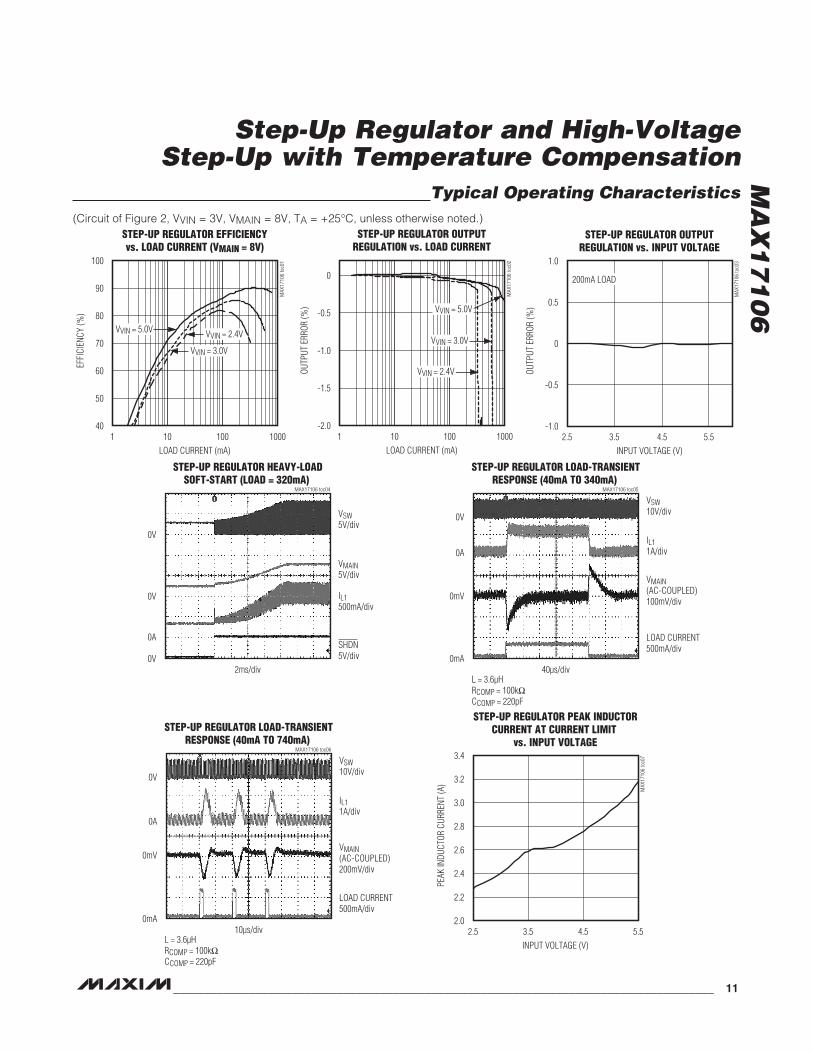
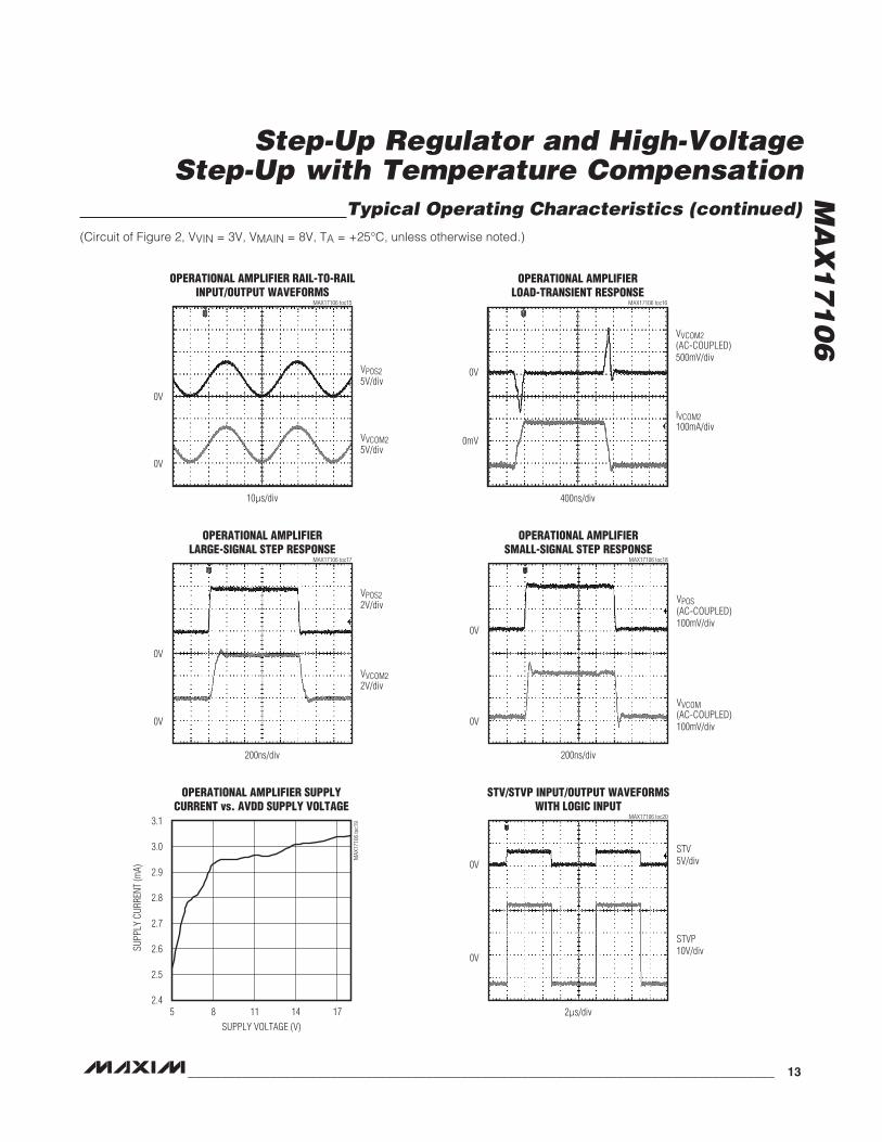
Typical Operating Characteristics(Circuit of Figure 2, VVIN = 3V, VMAIN = 8V, TA = +25NC, unless otherwise noted.)
STEP-UP REGULATOR EFFICIENCYvs. LOAD CURRENT (VMAIN = 8V)
MAX
1710
6 to
c01
LOAD CURRENT (mA)
EFFI
CIEN
CY (%
)
10010
50
60
70
80
90
100
401 1000
VVIN = 5.0V
VVIN = 3.0V
VVIN = 2.4V
STEP-UP REGULATOR OUTPUTREGULATION vs. LOAD CURRENT
MAX
1710
6 to
c02
LOAD CURRENT (mA)
OUTP
UT E
RROR
(%)
10010
-1.5
-1.0
-0.5
0
-2.01 1000
VVIN = 5.0V
VVIN = 3.0V
VVIN = 2.4V
STEP-UP REGULATOR OUTPUTREGULATION vs. INPUT VOLTAGE
MAX
1710
6 to
c03
INPUT VOLTAGE (V)
OUTP
UT E
RROR
(%)
5.54.53.5
-0.5
0
0.5
1.0
-1.02.5
200mA LOAD
STEP-UP REGULATOR HEAVY-LOADSOFT-START (LOAD = 320mA)
MAX17106 toc04
SHDN5V/div
IL1500mA/div
VSW5V/div
VMAIN5V/div
0V
0V
0V
0A
2ms/div
STEP-UP REGULATOR LOAD-TRANSIENTRESPONSE (40mA TO 340mA)
MAX17106 toc05
LOAD CURRENT500mA/div
L = 3.6µHRCOMP = 100kICCOMP = 220pF
IL11A/div
VSW10V/div
VMAIN(AC-COUPLED)100mV/div
0A
0V
0mV
0mA40µs/div
STEP-UP REGULATOR LOAD-TRANSIENTRESPONSE (40mA TO 740mA)
MAX17106 toc06
LOAD CURRENT500mA/div
L = 3.6µHRCOMP = 100kICCOMP = 220pF
IL11A/div
VSW10V/div
VMAIN(AC-COUPLED)200mV/div
0A
0V
0mV
0mA10µs/div
STEP-UP REGULATOR PEAK INDUCTORCURRENT AT CURRENT LIMIT
vs. INPUT VOLTAGE
MAX
1710
6 to
c07
INPUT VOLTAGE (V)
PEAK
INDU
CTOR
CUR
RENT
(A)
4.53.5
2.2
2.4
2.6
2.8
3.0
3.2
3.4
2.02.5 5.5
Step-Up Regulator and High-Voltage Step-Up with Temperature Compensation
MA
X1
71
06
12 _____________________________________________________________________________________
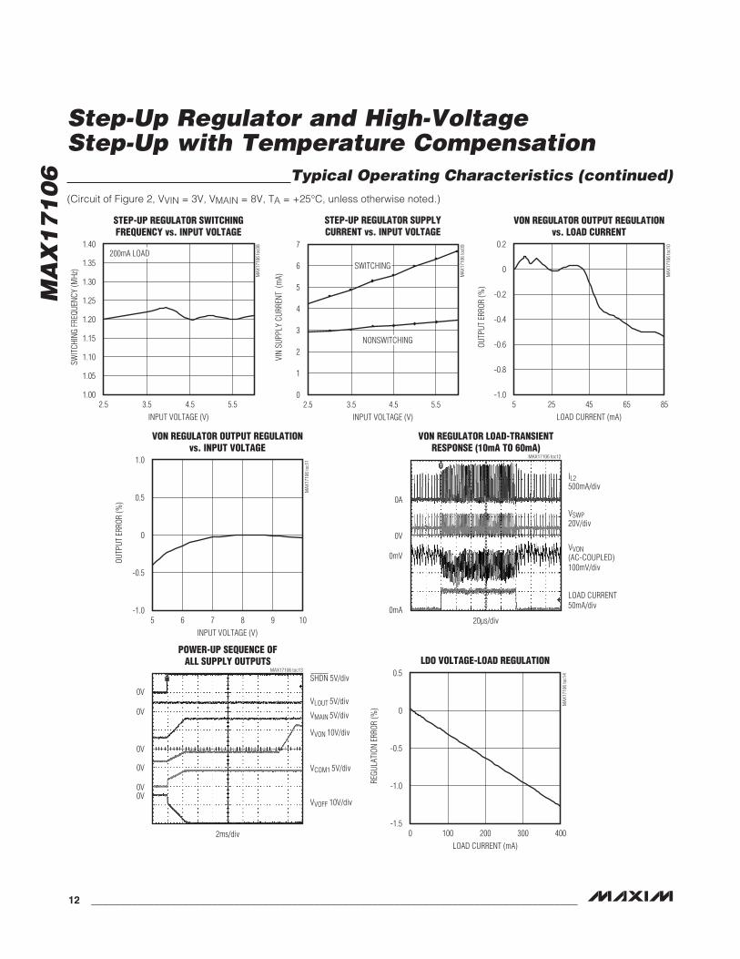
Typical Operating Characteristics (continued)(Circuit of Figure 2, VVIN = 3V, VMAIN = 8V, TA = +25NC, unless otherwise noted.)
STEP-UP REGULATOR SWITCHINGFREQUENCY vs. INPUT VOLTAGE
MAX
1710
6 to
c08
INPUT VOLTAGE (V)
SWIT
CHIN
G FR
EQUE
NCY
(MHz
)
5.54.53.5
1.05
1.10
1.15
1.20
1.25
1.30
1.35
1.40
1.002.5
200mA LOAD
STEP-UP REGULATOR SUPPLYCURRENT vs. INPUT VOLTAGE
MAX
1710
6 to
c09
INPUT VOLTAGE (V)
VIN
SUPP
LY C
URRE
NT (
mA)
5.54.53.5
1
2
3
4
5
6
7
02.5
NONSWITCHING
SWITCHING
VON REGULATOR OUTPUT REGULATIONvs. LOAD CURRENT
MAX
1710
6 to
c10
LOAD CURRENT (mA)
OUTP
UT E
RROR
(%)
654525
-0.8
-0.6
-0.4
-0.2
0
0.2
-1.05 85
VON REGULATOR OUTPUT REGULATIONvs. INPUT VOLTAGE
MAX
1710
6 to
c11
INPUT VOLTAGE (V)
OUTP
UT E
RROR
(%)
9876
-0.5
0
0.5
1.0
-1.05 10
VON REGULATOR LOAD-TRANSIENTRESPONSE (10mA TO 60mA)
MAX17106 toc12
LOAD CURRENT50mA/div
VVON(AC-COUPLED)100mV/div
IL2500mA/div
VSWP20V/div
0A
0V
0mV
0mA20µs/div
POWER-UP SEQUENCE OFALL SUPPLY OUTPUTS
MAX17106 toc13
VVOFF 10V/div
VCOM1 5V/div
VVON 10V/div
VMAIN 5V/div
VLOUT 5V/div
SHDN 5V/div
0V0V
0V
0V
0V
0V
2ms/div
LDO VOLTAGE-LOAD REGULATION
MAX
1710
6 to
c14
LOAD CURRENT (mA)
REGU
LATI
ON E
RROR
(%)
300200100
-1.0
-0.5
0
0.5
-1.50 400
Step-Up Regulator and High-Voltage Step-Up with Temperature Compensation
MA
X1
71
06
______________________________________________________________________________________ 13
Typical Operating Characteristics (continued)(Circuit of Figure 2, VVIN = 3V, VMAIN = 8V, TA = +25NC, unless otherwise noted.)
OPERATIONAL AMPLIFIERLOAD-TRANSIENT RESPONSE
MAX17106 toc16
VVCOM2(AC-COUPLED)500mV/div
IVCOM2100mA/div
0mV
0V
400ns/div
OPERATIONAL AMPLIFIERLARGE-SIGNAL STEP RESPONSE
MAX17106 toc17
VPOS22V/div
VVCOM22V/div
0V
0V
200ns/div
OPERATIONAL AMPLIFIERSMALL-SIGNAL STEP RESPONSE
MAX17106 toc18
VPOS(AC-COUPLED)100mV/div
VVCOM(AC-COUPLED)100mV/div0V
0V
200ns/div
OPERATIONAL AMPLIFIER SUPPLYCURRENT vs. AVDD SUPPLY VOLTAGE
MAX
1710
6 to
c19
SUPPLY VOLTAGE (V)
SUPP
LY C
URRE
NT (m
A)
1714118
2.5
2.6
2.7
2.8
2.9
3.0
3.1
2.45
STV/STVP INPUT/OUTPUT WAVEFORMSWITH LOGIC INPUT
MAX17106 toc20
STV5V/div
STVP10V/div
0V
0V
2Fs/div
OPERATIONAL AMPLIFIER RAIL-TO-RAILINPUT/OUTPUT WAVEFORMS
MAX17106 toc15
VPOS25V/div
VVCOM25V/div
0V
0V
10Fs/div

Step-Up Regulator and High-Voltage Step-Up with Temperature Compensation
MA
X1
71
06
14 _____________________________________________________________________________________
Typical Operating Characteristics (continued)(Circuit of Figure 2, VVIN = 3V, VMAIN = 8V, TA = +25NC, unless otherwise noted.)
STV RISING EDGE PROPAGATION DELAY
MAX17106 toc22
STV2V/div
STVP10V/div
0V
0V
20ns/div
OE/CKV RISING EDGEPROPAGATION DELAY
MAX17106 toc23
OE5V/div
CKV10V/div
0V
0V
100ns/div
STV FALLING EDGEPROPAGATION DELAY
MAX17106 toc24
STV2V/div
STVP10V/div
0V
0V
20ns/div
OE/CKV FALLING EDGEPROPAGATION DELAY
MAX17106 toc25
OE5V/div
CKV10V/div
0V
0V
100ns/div
CALIBRATOR FULL-SCALE UPWARDSTEP RESPONSE
MAX17106 toc26
VVCOM11V/div
VRSET200mV/div
0V
0V
2Fs/div
CPV, OE/CKV, AND CKVB INPUT/OUTPUT WAVEFORMS WITH LOGIC INPUT
(STV = 0V, CLOAD = 5.0nF, AND 50I, R1, R2 = 200I)MAX17106 toc21
CPV5V/div
OE5V/div
CKV20V/div
CKVB20V/div0V
0V
0V
0V
2Fs/div
CALIBRATOR FULL-SCALEDOWNWARD STEP RESPONSE
MAX17106 toc27
VVCOM11V/div
VRSET200mV/div
0V
0V
2Fs/div
Step-Up Regulator and High-Voltage Step-Up with Temperature Compensation
MA
X1
71
06
______________________________________________________________________________________ 15
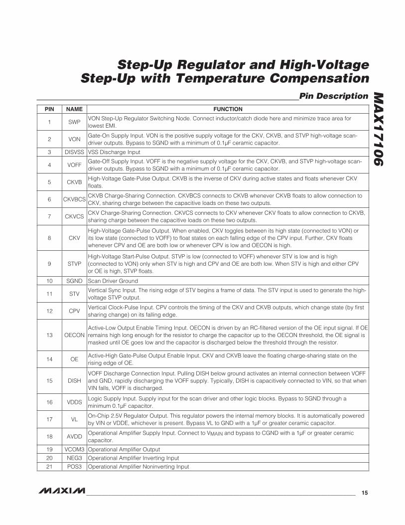
Pin DescriptionPIN NAME FUNCTION
1 SWPVON Step-Up Regulator Switching Node. Connect inductor/catch diode here and minimize trace area for lowest EMI.
2 VONGate-On Supply Input. VON is the positive supply voltage for the CKV, CKVB, and STVP high-voltage scan-driver outputs. Bypass to SGND with a minimum of 0.1FF ceramic capacitor.
3 DISVSS VSS Discharge Input
4 VOFFGate-Off Supply Input. VOFF is the negative supply voltage for the CKV, CKVB, and STVP high-voltage scan-driver outputs. Bypass to SGND with a minimum of 0.1FF ceramic capacitor.
5 CKVBHigh-Voltage Gate-Pulse Output. CKVB is the inverse of CKV during active states and floats whenever CKV floats.
6 CKVBCSCKVB Charge-Sharing Connection. CKVBCS connects to CKVB whenever CKVB floats to allow connection to CKV, sharing charge between the capacitive loads on these two outputs.
7 CKVCSCKV Charge-Sharing Connection. CKVCS connects to CKV whenever CKV floats to allow connection to CKVB, sharing charge between the capacitive loads on these two outputs.
8 CKVHigh-Voltage Gate-Pulse Output. When enabled, CKV toggles between its high state (connected to VON) or its low state (connected to VOFF) to float states on each falling edge of the CPV input. Further, CKV floats whenever CPV and OE are both low or whenever CPV is low and OECON is high.
9 STVPHigh-Voltage Start-Pulse Output. STVP is low (connected to VOFF) whenever STV is low and is high (connected to VON) only when STV is high and CPV and OE are both low. When STV is high and either CPV or OE is high, STVP floats.
10 SGND Scan Driver Ground
11 STVVertical Sync Input. The rising edge of STV begins a frame of data. The STV input is used to generate the high-voltage STVP output.
12 CPVVertical Clock-Pulse Input. CPV controls the timing of the CKV and CKVB outputs, which change state (by first sharing change) on its falling edge.
13 OECONActive-Low Output Enable Timing Input. OECON is driven by an RC-filtered version of the OE input signal. If OE remains high long enough for the resistor to charge the capacitor up to the OECON threshold, the OE signal is masked until OE goes low and the capacitor is discharged below the threshold through the resistor.
14 OEActive-High Gate-Pulse Output Enable Input. CKV and CKVB leave the floating charge-sharing state on the rising edge of OE.
15 DISHVOFF Discharge Connection Input. Pulling DISH below ground activates an internal connection between VOFF and GND, rapidly discharging the VOFF supply. Typically, DISH is capacitively connected to VIN, so that when VIN falls, VOFF is discharged.
16 VDDSLogic Supply Input. Supply input for the scan driver and other logic blocks. Bypass to SGND through a minimum 0.1FF capacitor.
17 VLOn-Chip 2.5V Regulator Output. This regulator powers the internal memory blocks. It is automatically powered by VIN or VDDE, whichever is present. Bypass VL to GND with a 1FF or greater ceramic capacitor.
18 AVDDOperational Amplifier Supply Input. Connect to VMAIN and bypass to CGND with a 1FF or greater ceramic capacitor.
19 VCOM3 Operational Amplifier Output
20 NEG3 Operational Amplifier Inverting Input
21 POS3 Operational Amplifier Noninverting Input
Step-Up Regulator and High-Voltage Step-Up with Temperature Compensation
MA
X1
71
06
16 _____________________________________________________________________________________
Pin Description (continued)PIN NAME FUNCTION
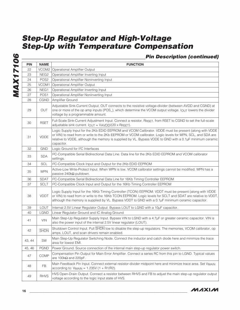
22 VCOM2 Operational Amplifier Output
23 NEG2 Operational Amplifier Inverting Input
24 POS2 Operational Amplifier Noninverting Input
25 VCOM1 Operational Amplifier Output
26 NEG1 Operational Amplifier Inverting Input
27 POS1 Operational Amplifier Noninverting Input
28 CGND Amplifier Ground
29 OUTAdjustable Sink-Current Output. OUT connects to the resistive voltage-divider (between AVDD and CGND) at one or more of the op amp inputs (POS_), which determine the VCOM output voltage. IOUT lowers the divider voltage by a programmable amount.
30 RSETFull-Scale Sink-Current Adjustment Input. Connect a resistor, RRSET, from RSET to CGND to set the full-scale adjustable sink current. IOUT = VAVDD/(20 x RRSET).
31 VDDE
Logic Supply Input for the 2Kb EDID EEPROM and VCOM Calibrator. VDDE must be present (along with VDDE or VIN) to read from or write to the 2Kb EEPROM or VCOM calibrator. Logic levels for WPN, SCL, and SDA are relative to VDDE, although the memory is supplied by VL. Bypass VDDE to GND with a 0.1FF minimum ceramic capacitor.
32 GND Logic Ground for I2C Interfaces
33 SDAI2C-Compatible Serial Bidirectional Data Line. Data line for the 2Kb EDID EEPROM and VCOM calibrator settings.
34 SCL I2C-Compatible Clock Input and Output for the 2Kb EDID EEPROM
35 WPNActive-Low Write-Protect Input. When WPN is low, VCOM calibrator settings cannot be modified. WPN has a passive 240kI pulldown.
36 SDAT I2C-Compatible Serial Bidirectional Data Line for 16Kb Timing Controller EEPROM
37 SCLT I2C-Compatible Clock Input and Output for the 16Kb Timing Controller EEPROM
38 VDDTLogic Supply Input for the 16Kb Timing Controller (TCON) EEPROM. VDDT must be present (along with VDDE or VIN) to read from or write to the 16Kb TCON EEPROM. Logic levels for SCLT and SDAT are relative to VDDT, although the memory is supplied by VL. Bypass VDDT to GND with a 0.1FF minimum ceramic capacitor.
39 LOUT Internal 2.5V Linear Regulator Output. Bypass LOUT to LGND with a 10FF capacitor.
40 LGND Linear Regulator Ground and IC Analog Ground
41 VINMain Step-Up Regulator Supply Input. Bypass VIN to LGND with a 4.7FF or greater ceramic capacitor. VIN is also the power input of the internal 2.5V linear regulator (LOUT).
42 SHDNShutdown Control Input. Pull SHDN low to disable the step-up regulators. The memories, VCOM calibrator, op amps, LOUT, and scan drivers remain enabled.
43, 44 SWMain Step-Up Regulator Switching Node. Connect the inductor and catch diode here and minimize the trace area for lowest EMI.
45, 46 PGND Power Ground. Source connection of the internal main step-up regulator power switch.
47 COMPCompensation Pin Output for Main Error Amplifier. Connect a series RC from this pin to LGND. Typical values are 100kI and 220pF.
48 FBMain Feedback Pin Input. Connect external resistor-divider midpoint here and minimize trace area. Set VMAIN according to: VMAIN = 1.235V (1 + R1/R2).
49 RHVSHVS Open-Drain Output. Connect a resistor between RHVS and FB to adjust the main step-up regulator output voltage according to the logic input state of HVS.
Step-Up Regulator and High-Voltage Step-Up with Temperature Compensation
MA
X1
71
06
______________________________________________________________________________________ 17
Pin Description (continued)PIN NAME FUNCTION
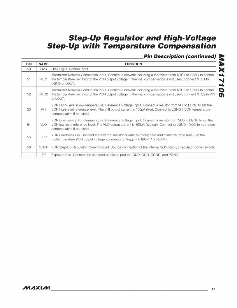
50 HVS HVS Digital Control Input
51 NTC1Thermistor Network Connection Input. Connect a network including a thermistor from NTC1 to LGND to control the temperature behavior of the VON output voltage. If thermal compensation is not used, connect NTC1 to LGND or LOUT.
52 NTC2Thermistor Network Connection Input. Connect a network including a thermistor from NTC2 to LGND to control the temperature behavior of the VON output voltage. If thermal compensation is not used, connect NTC2 to VIN or LOUT.
53 VHIVON High-Level (Low-Temperature) Reference Voltage Input. Connect a resistor from VHI to LGND to set the VON high-level reference level. The VHI output current is 100FA (typ). Connect to LGND if VON temperature compensation if not used.
54 VLOVON Low-Level (High-Temperature) Reference Voltage Input. Connect a resistor from VLO to LGND to set the VON low-level reference level. The VLO output current is 100FA (typical). Connect to LGND if VON temperature compensation if not used.
55 FBPVON Feedback Pin. Connect the external resistor-divider midpoint here and minimize trace area. Set the midtemperature VON output voltage according to: VVON = 0.893V (1 + R3/R4).
56 GNDP VON Step-Up Regulator Power Ground. Source connection of the internal VON step-up regulator power switch.
— EP Exposed Pad. Connect the exposed backside pad to LGND, GND, CGND, and PGND.

Step-Up Regulator and High-Voltage Step-Up with Temperature Compensation
MA
X1
71
06
18 _____________________________________________________________________________________
Figure 2. Typical Operating Circuit
VGOFF-12V, 20mA
0.1FF
0.1FF
1FF
0.1FF20kI20kI
0.1FF
0.1FF
3nF
SGND
SGND
20kI
20kI
20kI
D3
D2
D4
L13.6FH
L23.6FH
C110FF
C210FF
C3, C42 x 4.7FF
C51FF
R1200kI
R234kI
RCOMP100kI
R3230kI
R5230kI
RSET25kI
14kI
7kI
R6200kI
R410kI
CCOMP220pF
RHVS
47pF
1FF
22pF
100pF
D1VMAIN
8V, 300mA
TO VCOMBACKPLANE
*22V IS NOMINAL OR MIDTEMPERATURE SETTING
COMP
SW
PGND
CGND
VCOM2
POS2
NEG2
FB
AVDD
VIN
RSET
SHDN
OECON
STV
DISH
OE
CPV
OUT
SYSTEM
PANEL
R5200I
R6200I
VCOM3
POS3
NEG3
VCOM1
POS1
NEG1
STVP
CKV
CKVB
VOFF
CKVCS
CKVCSB
HVS
RHVS
SWP
FBP
SDAT
SCLT
TCONI2C BUS
DISVSS
DISVSS
PGND
SW
PGND
NTC1NTC2
VHI
VLO
VDDT
VL
LOUT
LGND
VSS
VVIN2.4V TO 5.5V
VLDO2.5V, 300mA
VGON22V, 20mA*
VMAIN
VVIN
SDA
SCL
DVR/EDID
I2C BUS WPN
VDDE
GND
VVIN
VDDS
SGND
VVIN
VONVGON
VGOFF
1FF
MAX17106
Step-Up Regulator and High-Voltage Step-Up with Temperature Compensation
MA
X1
71
06
______________________________________________________________________________________ 19
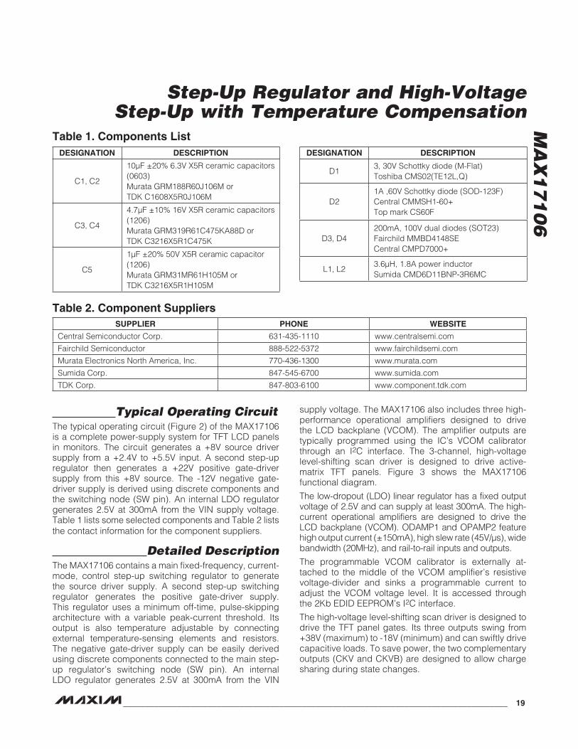
Typical Operating CircuitThe typical operating circuit (Figure 2) of the MAX17106 is a complete power-supply system for TFT LCD panels in monitors. The circuit generates a +8V source driver supply from a +2.4V to +5.5V input. A second step-up regulator then generates a +22V positive gate-driver supply from this +8V source. The -12V negative gate-driver supply is derived using discrete components and the switching node (SW pin). An internal LDO regulator generates 2.5V at 300mA from the VIN supply voltage. Table 1 lists some selected components and Table 2 lists the contact information for the component suppliers.
Detailed DescriptionThe MAX17106 contains a main fixed-frequency, current-mode, control step-up switching regulator to generate the source driver supply. A second step-up switching regulator generates the positive gate-driver supply. This regulator uses a minimum off-time, pulse-skipping architecture with a variable peak-current threshold. Its output is also temperature adjustable by connecting external temperature-sensing elements and resistors. The negative gate-driver supply can be easily derived using discrete components connected to the main step-up regulator’s switching node (SW pin). An internal LDO regulator generates 2.5V at 300mA from the VIN
supply voltage. The MAX17106 also includes three high-performance operational amplifiers designed to drive the LCD backplane (VCOM). The amplifier outputs are typically programmed using the IC’s VCOM calibrator through an I2C interface. The 3-channel, high-voltage level-shifting scan driver is designed to drive active-matrix TFT panels. Figure 3 shows the MAX17106 functional diagram.
The low-dropout (LDO) linear regulator has a fixed output voltage of 2.5V and can supply at least 300mA. The high-current operational amplifiers are designed to drive the LCD backplane (VCOM). ODAMP1 and OPAMP2 feature high output current (Q150mA), high slew rate (45V/µs), wide bandwidth (20MHz), and rail-to-rail inputs and outputs.
The programmable VCOM calibrator is externally at-tached to the middle of the VCOM amplifier’s resistive voltage-divider and sinks a programmable current to adjust the VCOM voltage level. It is accessed through the 2Kb EDID EEPROM’s I2C interface.
The high-voltage level-shifting scan driver is designed to drive the TFT panel gates. Its three outputs swing from +38V (maximum) to -18V (minimum) and can swiftly drive capacitive loads. To save power, the two complementary outputs (CKV and CKVB) are designed to allow charge sharing during state changes.
Table 2. Component Suppliers
Table 1. Components List
SUPPLIER PHONE WEBSITE
Central Semiconductor Corp. 631-435-1110 www.centralsemi.com
Fairchild Semiconductor 888-522-5372 www.fairchildsemi.com
Murata Electronics North America, Inc. 770-436-1300 www.murata.com
Sumida Corp. 847-545-6700 www.sumida.com
TDK Corp. 847-803-6100 www.component.tdk.com
DESIGNATION DESCRIPTION
C1, C2
10FF Q20% 6.3V X5R ceramic capacitors (0603)Murata GRM188R60J106M orTDK C1608X5R0J106M
C3, C4
4.7FF Q10% 16V X5R ceramic capacitors (1206)Murata GRM319R61C475KA88D orTDK C3216X5R1C475K
C5
1FF Q20% 50V X5R ceramic capacitor (1206)Murata GRM31MR61H105M orTDK C3216X5R1H105M
DESIGNATION DESCRIPTION
D13, 30V Schottky diode (M-Flat)Toshiba CMS02(TE12L,Q)
D21A ,60V Schottky diode (SOD-123F)Central CMMSH1-60+Top mark CS60F
D3, D4200mA, 100V dual diodes (SOT23)Fairchild MMBD4148SECentral CMPD7000+
L1, L23.6FH, 1.8A power inductorSumida CMD6D11BNP-3R6MC

Step-Up Regulator and High-Voltage Step-Up with Temperature Compensation
MA
X1
71
06
20 _____________________________________________________________________________________
Figure 3. Functional Diagram
1.8AMINSTEPUP
2KbEEPROM
7
VOFF
SGND
0.2AMINSTEPUP
SEQUENCE
2.5VLDO
DVREEPROM
SCANDRIVER LOGIC
AND GATEDRIVERS
LGNDVL2.5VLDO
GND
DISVSS
50kI
CONTROL
VON
VINUVLO
16KbEEPROM
VVOFF
VMAIN
VVON
LGND
TO VCOMBACKPLANE
COMP
SW
PGND
CGND
FB
AVDD
VIN
RSET
SHDN
OECON
STV
DISH
OE
CPV
OUTSYSTEM
PANEL
VCOM3
POS3
NEG3
STVP
CKV
CKVB
VOFF
CKVCS
CKVCSB
HVS
RHVS
SWP
FBP
SDAT
SCLT
TCONI2C BUS
PGND
NTC1
NTC2
VHI
VLO
VDDT
LOUT
LGND
VVIN
VLOUT
VDDT
VVIN
VVIN
SDA
SCL
DVR/EDID
I2C BUSWPN
VDDE
VDDE
VDDSVVIN
VONVGON
VVOFFs
VCOM2
POS2
NEG2
VCOM1
POS1
NEG1
LGND
250I
50kI
MAX17106

Step-Up Regulator and High-Voltage Step-Up with Temperature Compensation
MA
X1
71
06
______________________________________________________________________________________ 21
Main Step-Up RegulatorThe main step-up regulator employs a current-mode, fixed-frequency PWM architecture to maximize loop bandwidth and provide fast transient response to pulsed loads that are typical for TFT LCD panel source drivers. The 1.2MHz high-switching frequency allows the use of low-profile inductors and ceramic capacitors to minimize the thickness of LCD panel designs. The integrated high-efficiency MOSFET reduces the number of external components required. The output voltage can be set from VIN to 18V with an external resistive voltage-divider.
The regulator controls the output voltage and the power delivered to the output by modulating duty cycle D of the internal power MOSFET in each switching cycle.
Figure 4 shows the functional diagram of the step-up regulator. An error amplifier compares the signal at FB to 1.24V and changes the COMP output. The voltage at COMP sets the peak inductor current. As the load varies, the error amplifier sources or sinks current to the COMP output accordingly to produce the inductor peak current necessary to service the load. To maintain stability at high duty cycles, a slope compensation signal is summed with the current-sense signal.
On the rising edge of the internal clock, the controller sets a flip-flop, turning on the n-channel MOSFET and applying the input voltage across the inductor. The current through the inductor ramps up linearly, storing energy in its magnetic field. Once the sum of the current-feedback signal and the slope compensation exceed the COMP voltage, the controller resets the flip-flop and turns off the MOSFET. Since the inductor current is continuous, a transverse potential develops across the inductor that turns on diode D1. The voltage across the inductor then becomes the difference between the output voltage and the input voltage. This discharge condition forces the current through the inductor to ramp back down, transferring the energy stored in the magnetic field to the output capacitor and the load. The MOSFET remains off for the rest of the clock cycle.
VON Positive Gate-Driver Step-Up Regulator
The VON step-up regulator employs a minimum off-time, modified fixed-current threshold, forced-discontinuous mode architecture for simple control and stable behavior with minimal output bypass. The fixed-current threshold was modified to a variable threshold that adjusts the threshold to lower losses when lightly loaded. Under light load, the VON regulator may also skip pulses.
Figure 4. Main Step-Up Regulator Block Diagram
SOFT-START
1.2MHzOSCILLATOR
TO FAULT LOGIC
1.24V
FB
SW
ILIMCOMPARATOR
ILIMIT
CURRENTSENSE
PGND
COMP
CLOCK
ERROR AMPLIFIER
PWMCOMPARATOR
SLOPE COMP
FAULTCOMPARATOR
LOGIC AND DRIVER
MAX17106
Step-Up Regulator and High-Voltage Step-Up with Temperature Compensation
MA
X1
71
06
22 _____________________________________________________________________________________
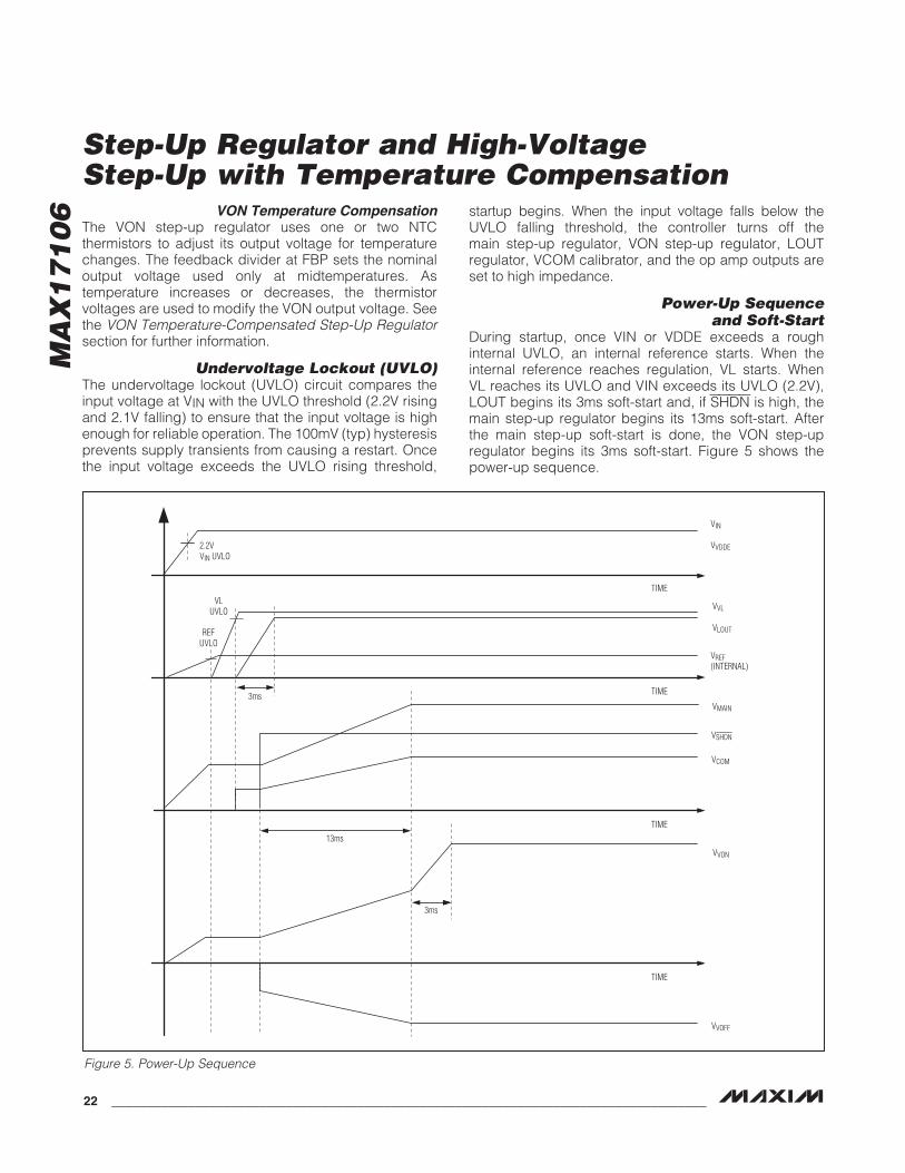
VON Temperature CompensationThe VON step-up regulator uses one or two NTC thermistors to adjust its output voltage for temperature changes. The feedback divider at FBP sets the nominal output voltage used only at midtemperatures. As temperature increases or decreases, the thermistor voltages are used to modify the VON output voltage. See the VON Temperature-Compensated Step-Up Regulator section for further information.
Undervoltage Lockout (UVLO)The undervoltage lockout (UVLO) circuit compares the input voltage at VIN with the UVLO threshold (2.2V rising and 2.1V falling) to ensure that the input voltage is high enough for reliable operation. The 100mV (typ) hysteresis prevents supply transients from causing a restart. Once the input voltage exceeds the UVLO rising threshold,
startup begins. When the input voltage falls below the UVLO falling threshold, the controller turns off the main step-up regulator, VON step-up regulator, LOUT regulator, VCOM calibrator, and the op amp outputs are set to high impedance.
Power-Up Sequence and Soft-Start
During startup, once VIN or VDDE exceeds a rough internal UVLO, an internal reference starts. When the internal reference reaches regulation, VL starts. When VL reaches its UVLO and VIN exceeds its UVLO (2.2V), LOUT begins its 3ms soft-start and, if SHDN is high, the main step-up regulator begins its 13ms soft-start. After the main step-up soft-start is done, the VON step-up regulator begins its 3ms soft-start. Figure 5 shows the power-up sequence.
Figure 5. Power-Up Sequence
VMAIN
VIN
VVDDE
VSHDN
VREF(INTERNAL)
VVON
VVOFF
2.2VVIN UVLO
REFUVLO
VVL
VLOUT
VCOM
3ms
3ms
13ms
TIME
TIME
TIME
TIME
VLUVLO
Step-Up Regulator and High-Voltage Step-Up with Temperature Compensation
MA
X1
71
06
______________________________________________________________________________________ 23
The soft-start routine minimizes the inrush current and voltage overshoot, and ensures a well-defined startup behavior. The LOUT and VON 3ms soft-start routines are a digitally controlled output voltage ramp. The main step-up’s 13ms soft-start instead controls the step-up regulator’s current limit, ramping it slowly from zero up to the full current limit over the 13ms period. The step-up regulator’s output typically reaches regulation before the 13ms period finishes.
Operational AmplifiersThe MAX17106 has three operational amplifiers. These operational amplifiers are typically used to drive the LCD backplane (VCOM) or the gamma-correction divider string. OPAMP1 and OPAMP2 feature Q150mA output short-circuit current, 45V/Fs slew rate, and 20MHz -3dB bandwidth. The rail-to-rail input and output capability maximizes system flexibility.
Short-Circuit Current LimitThe operational amplifiers deliver a minimum short-circuit current of Q150mA if the output is directly shorted to AVDD or to GND. If the short-circuit condition persists, the junction temperature of the IC rises until it reaches the thermal-shutdown threshold (+160NC typ). Once the junction temperature reaches the thermal-shutdown threshold, an internal thermal sensor temporarily shuts off all the IC’s outputs. See the Thermal-Overload Protection section for details.
Driving Pure Capacitive LoadsThe operational amplifiers are typically used to drive the LCD backplane (VCOM) or the gamma-correction divider string. The LCD backplane consists of a distributed series capacitance and resistance, a load that can be easily driven by the operational amplifiers. However, if an
operational amplifier is used in an application with a pure capacitive load, steps must be taken to ensure stable operation. As the operational amplifier’s capacitive load increases, the amplifier’s bandwidth decreases and gain peaking increases. A 5I to 50I small resistor placed between OUT and the capacitive load reduces peaking, but also reduces the gain. An alternative method of reducing peaking is to place a series RC network (snubber) in parallel with the capacitive load. The RC network does not continuously load the output or reduce the gain. Typical values of the resistor are between 100I and 200I, and the typical value of the capacitor is 10nF.
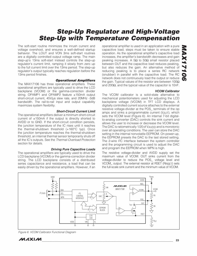
VCOM CalibratorThe VCOM calibrator is a solid-state alternative to mechanical potentiometers used for adjusting the LCD backplane voltage (VCOM) in TFT LCD displays. A digitally controlled current source attaches to the external resistive voltage-divider at the POS_ terminals of the op amps and sinks a programmable current (IOUT), which sets the VCOM level (Figure 6). An internal 7-bit digital-to-analog converter (DAC) controls the sink current and allows the user to increase or decrease the VCOM level. The DAC is ratiometrically 1/20 of VAVDD and is monotonic over all operating conditions. The user can store the DAC setting in the internal nonvolatile EEPROM. On power-up, the EEPROM presets the DAC to the last stored setting. The 2-wire I2C interface between the system controller and the programming circuit is used to adjust the DAC and program the EEPROM when WPN is high.
The resistive voltage-divider and AVDD supply set the maximum value of VCOM. OUT sinks current from the voltage-divider to reduce the POS_ voltage level and VCOM_ output. The external resistor at RSET (RRSET) sets the full-scale sink current and the minimum value of VCOM.
Figure 6. VCOM Calibrator Functional Diagram
SDA
SCL
AVDD
RSET
RSET
OUTIOUT
VLVDDE VIN
R6
R5
VCOM_
VMAIN
EEPROMBLOCK
2.5VLDO
DAC
19R
R
7
7
VDDE
POS_
NEG_
WPN
VCOM
I2C BUS I2CCONTROL
INTERFACE
MAX17106
Step-Up Regulator and High-Voltage Step-Up with Temperature Compensation
MA
X1
71
06
24 _____________________________________________________________________________________
The VL LDO powers the EEPROM. The LDO can be powered by VDDE or VIN. However, VDDE must be supplied to read or write the EEPROM.
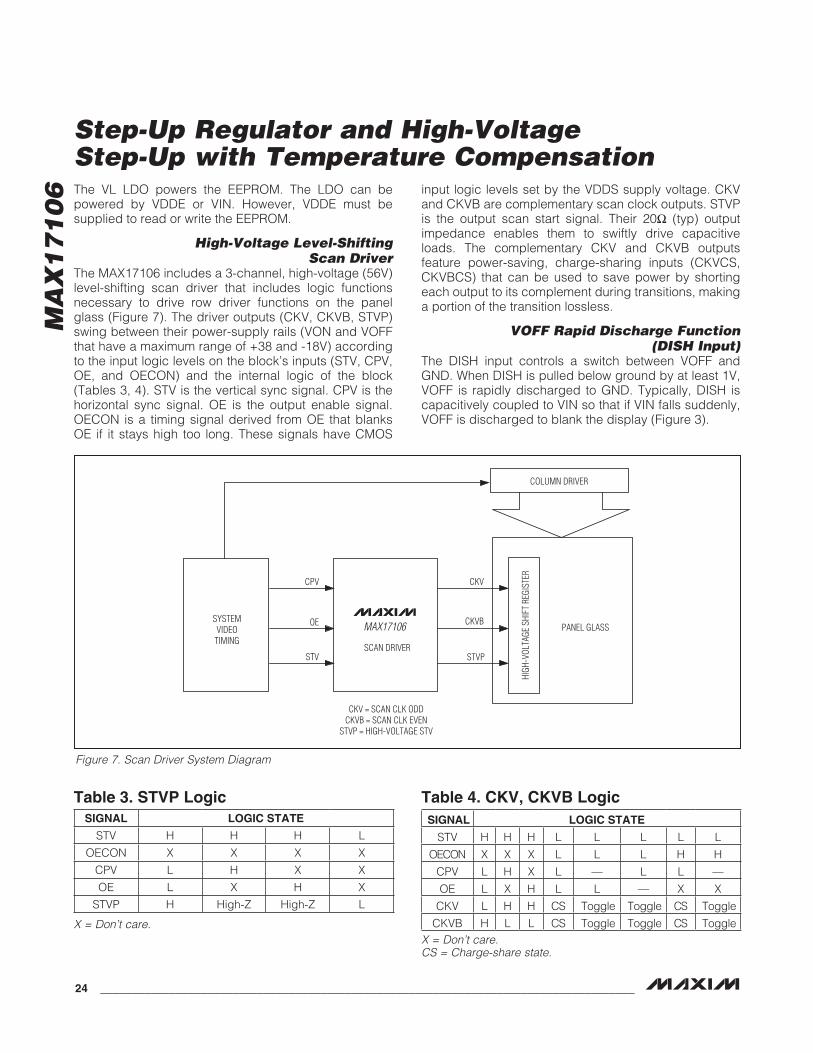
High-Voltage Level-Shifting Scan Driver
The MAX17106 includes a 3-channel, high-voltage (56V) level-shifting scan driver that includes logic functions necessary to drive row driver functions on the panel glass (Figure 7). The driver outputs (CKV, CKVB, STVP) swing between their power-supply rails (VON and VOFF that have a maximum range of +38 and -18V) according to the input logic levels on the block’s inputs (STV, CPV, OE, and OECON) and the internal logic of the block (Tables 3, 4). STV is the vertical sync signal. CPV is the horizontal sync signal. OE is the output enable signal. OECON is a timing signal derived from OE that blanks OE if it stays high too long. These signals have CMOS
input logic levels set by the VDDS supply voltage. CKV and CKVB are complementary scan clock outputs. STVP is the output scan start signal. Their 20I (typ) output impedance enables them to swiftly drive capacitive loads. The complementary CKV and CKVB outputs feature power-saving, charge-sharing inputs (CKVCS, CKVBCS) that can be used to save power by shorting each output to its complement during transitions, making a portion of the transition lossless.
VOFF Rapid Discharge Function (DISH Input)
The DISH input controls a switch between VOFF and GND. When DISH is pulled below ground by at least 1V, VOFF is rapidly discharged to GND. Typically, DISH is capacitively coupled to VIN so that if VIN falls suddenly, VOFF is discharged to blank the display (Figure 3).
Figure 7. Scan Driver System Diagram
Table 3. STVP Logic
X = Don’t care.
Table 4. CKV, CKVB Logic
X = Don’t care. CS = Charge-share state.
PANEL GLASS
COLUMN DRIVER
HIGH
-VOL
TAGE
SHI
FT R
EGIS
TER
SCAN DRIVER
SYSTEMVIDEOTIMING
STV
CKVB
STVP
CKV
OE
CPV
CKV = SCAN CLK ODDCKVB = SCAN CLK EVEN
STVP = HIGH-VOLTAGE STV
MAX17106
SIGNAL LOGIC STATE
STV H H H L
OECON X X X X
CPV L H X X
OE L X H X
STVP H High-Z High-Z L
SIGNAL LOGIC STATE
STV H H H L L L L L
OECON X X X L L L H H
CPV L H X L — L L —
OE L X H L L — X X
CKV L H H CS Toggle Toggle CS Toggle
CKVB H L L CS Toggle Toggle CS Toggle

______________________________________________________________________________________ 25
Step-Up Regulator, High-Voltage Step-Up with Temperature Compensation
MA
X1
71
06
VSS Rapid Discharge Function (DISVSS Input)
The DISVSS function shorts a negative panel terminal VSS connected at the DISVSS pin to the positive gate-driver rail VON when the IC powers down. Since these two supply rails have similar bypass capacitors (usually 20FF each), the final voltage on each supply should settle at the midvoltage between these two rails. The purpose of this function is to pull the negative rail substantially positive to discharge the LCD quickly. This function is only activated during power-down when VIN drops below its UVLO threshold.
Thermal-Overload ProtectionThe thermal-overload protection prevents excessive power dissipation from overheating the device. When the junction temperature exceeds TJ = +160NC, a thermal sensor temporarily activates the fault protection, which shuts down all the IC’s outputs, allowing the device to cool down. Once the device cools down by approximately 15NC, it automatically reactivates with a complete soft-start. The thermal-overload protection protects the controller in the event of fault conditions. For continuous operation, do not exceed the absolute maximum junction temperature rating of +150NC.
Design ProcedureMain Step-Up Regulator
Inductor SelectionThe minimum inductance value, peak current rating, and series resistance are factors to consider when selecting the inductor. These factors influence the converter’s efficiency, maximum output load capability, transient response time, and output-voltage ripple. Physical size and cost are also important factors to be considered.
The maximum output current, input voltage, output voltage, and switching frequency determine the inductor value. Very-high-inductance values minimize the current ripple and therefore reduce the peak current, thereby decreasing core losses in the inductor and I2R losses in the entire power path. However, large inductor values also require more energy storage and more turns of wire, which increase physical size and can increase I2R losses in the inductor. Low inductance values decrease the physical size but increase the current ripple and peak current. Finding the best inductor involves choosing the best compromise between circuit efficiency, inductor size, and cost. The equations used here include a constant called LIR, which is the ratio of the inductor peak-to-peak ripple current to the average DC inductor current at the full load current. The best trade-off between
inductor size and circuit efficiency for step-up regulators generally has an LIR between 0.3 and 0.5. However, depending on the AC characteristics of the inductor core material and ratio of inductor resistance to other power-path resistances, the best LIR can shift up or down. If the inductor resistance is relatively high, more ripple can be accepted to reduce the number of turns required and increase the wire diameter. If the inductor resistance is relatively low, increasing inductance to lower the peak current can decrease losses throughout the power path. If extremely thin high-resistance inductors are used, as is common for LCD panel applications, the best LIR can increase to between 0.5 and 1.0.
Once a physical inductor is chosen, higher and lower values of the inductor should be evaluated for efficiency improvements in typical operating regions.
In Figure 2’s typical operating circuit, the LCD’s negative gate-off supply voltage is generated from an unregulated charge pump driven by the main step-up regulator’s SW node. The additional load on SW must therefore be considered in the inductance and current calculations. The LCD’s positive gate-on supply voltage is generated through the VON step-up regulator that is also supplied by VMAIN. Therefore, the main step-up’s effective maximum output current, IMAIN(EFF) becomes the sum of the maximum load current of the step-up regulator’s output, plus the contributions from the negative charge pump and the VON regulator:
MAIN(EFF) MAIN(MAX) NEG NEG
VON(MAX)ON
MAIN VON
I I I
IVV
= + η ×
+ ×η
where IMAIN(MAX) is the maximum step-up output current, ENEG is the number of negative charge-pump stages, INEG is the negative charge-pump output current, VON is the VON regulator’s maximum output voltage, IVON(MAX) is the VON regulator’s output current at the maximum output voltage, and EVON is the VON regulator’s efficiency under that condition and is approximately 90%.
Calculate the approximate inductor value using the typical input voltage (VIN), the maximum output current (IMAIN(EFF)), the expected efficiency EMAIN taken from an appropriate curve in the Typical Operating Characteristics, and an estimate of LIR based on the above discussion:
2IN MAIN IN MAIN
MAIN MAIN(EFF) OSC
V V - VL
V I f LIR
η = ×
Step-Up Regulator and High-Voltage Step-Up with Temperature Compensation
MA
X1
71
06
26 _____________________________________________________________________________________
Choose an available inductor value from an appropriate inductor family. Calculate the maximum DC input current at the minimum input voltage VIN(MIN) using conservation of energy and the expected efficiency at that operating point (EMAIN(MIN)) taken from an appropriate curve in the Typical Operating Characteristics:
MAIN(EFF) MAININ(DC,MAX)
IN(MIN) MAIN(MIN)
I VI
V
×=
× η
Calculate the ripple current at that operating point and the peak current required for the inductor:
( )IN(MIN) MAIN IN(MIN)RIPPLE
MAIN OSC
V V - VI
L V f
×=
× ×
RIPPLEPEAK IN(DC,MAX)
II I
2= +
The inductor’s saturation current rating and the MAX17106’s SW current limit should exceed IPEAK and the inductor’s DC current rating should exceed IIN(DC,MAX). For good efficiency, choose an inductor with less than 0.1I series resistance.
Considering the typical operating circuit (Figure 2), the maximum load current (IMAIN(MAX)) is 300mA, with an 8V output and a typical input voltage of 3V. Assume VON is 22V and its maximum load is 40mA. The effective full-load step-up current is:
MAIN(EFF)22V 40mA
I 300mA 2 20mA 462mA8V 90%
= + × + × =
Choosing an LIR of 0.3 and estimating efficiency of 85% at this operating point:
23V 8V - 3V 0.87L 3.59 H
8V 0.462A 1.2MHz 0.3 = ≈ ×
F
A 3.6FH inductor is chosen. Then, using the circuit’s typical input voltage (3V) and estimating efficiency of 80% at that operating point:
IN(DC,MAX)0.462A 8V
I 1.54A3V 0.8
×= ≈
×
The ripple current and the peak current at that input voltage are:
( )RIPPLE
3V 8V - 2.4VI 0.43A
3.6 H 8V 1.2MHz
×= ≈
× ×F
PEAK0.43A
I 1.54A 1.755A2
= + =
Output Capacitor SelectionThe total output voltage ripple has two components: the capacitive ripple caused by the charging and discharging of the output capacitance, and the ohmic ripple due to the capacitor’s equivalent series resistance (ESR):
RIPPLE RIPPLE(C) RIPPLE(ESR)
MAIN MAIN INRIPPLE(C)
OUT MAIN OSC
V V V
I V - VV
C V f
= +
≈
and:
RIPPLE(ESR) PEAK ESR(COUT)V I R≈
where IPEAK is the peak inductor current (see the Inductor Selection section). For ceramic capacitors, the output voltage ripple is typically dominated by VRIPPLE(C). The voltage rating and temperature characteristics of the output capacitor must also be considered.
Input Capacitor SelectionThe input capacitor (C1) reduces the current peaks drawn from the input supply and reduces noise injection into the IC. One 10FF ceramic capacitor is used in the typical operating circuit (Figure 2) because of the high source impedance seen in typical lab setups. Actual applications usually have much lower source impedance since the step-up regulator often runs directly from the output of another regulated supply. Typically, C1 can be reduced below the values used in the typical operating circuit. Ensure a low-noise supply at VIN by using adequate CIN.
Rectifier DiodeThe MAX17106’s high switching frequency demands a high-speed rectifier. Schottky diodes are recommended for most applications because of their fast recovery time and low forward voltage. In general, a 3A Schottky diode complements the internal MOSFET well.
Output Voltage SelectionThe output voltage of the main step-up regulator is adjusted by connecting a resistive voltage-divider from the output (VMAIN) to LGND with the center tap connected to FB (see Figure 2). Select R2 in the 10kI to 50kI range. Calculate R1 with the following equation:
MAIN
REF
VR1 R2 -1
V
= ×
where VREF, the step-up regulator’s feedback set point, is 1.235V (typ). Place R1 and R2 close to the IC.
Step-Up Regulator and High-Voltage Step-Up with Temperature Compensation
MA
X1
71
06
______________________________________________________________________________________ 27
HVS FunctionPulling the HVS pin high parallels RHVS with the lower resistor-divider R2, thus regulating VMAIN to a higher voltage VMAIN(HIGH). Pull the HVS pin to ground to disable this function:
HVSMAIN(HIGH)
REF
R1(R2 R )
V-1
V
=
Loop CompensationChoose RCOMP to set the high-frequency integrator gain for fast transient response. Choose CCOMP to set the integrator zero to maintain loop stability.
For low-ESR output capacitors, use the following equations to obtain stable performance and good transient response:
IN MAIN MAINCOMP
MAIN(MAX)
1000 V V CR
L I× × ×
≈×
OUT MAINCOMP
MAIN(MAX) COMP
V CC
10 I R×
≈× ×
To further optimize transient response, vary RCOMP in 20% steps and CCOMP in 50% steps while observing transient response waveforms.
VON Temperature-Compensated Step-Up Regulator
Selecting Component ValuesThe same procedure used to calculate the main step-up components can be used to calculate the VON regulator components. However, since the VON regulator application is very specific and the current is low, the component selection can be greatly simplified.
Choose an inductor with 2.7FH to 10FH inductance and a current rating of at least the SWP high-current limit value (2A typ). Within this range, a lower inductance value not only reduces cost and size, but also increases the single-cycle output ripple and thus improves stability. The output capacitor should be at least 1FF with a good dielectric that does not decrease in value excessively at high voltages. A larger capacitor value might be appropriate to account for the output capacitor’s voltage coefficient.
Set the output voltage by selecting proper values for R3 and R4, the FBP divider resistors. Select R4 in the 10kI to 50kI range and calculate R3 with the following equation:
ON(MID)
REF
VR3 R4 -1
V
= ×
where VON(MID) is the nominal midtemperature output voltage level and VREF is 0.893V (typ).
To improve the regulator’s performance, add a small feed-forward zero capacitor (for example, 20pF) in parallel with R3. This feed-forward capacitor increases the bandwidth of the regulator and reduces pulse grouping. An additional capacitor (for example, 100pF) placed in parallel with R4 can be used to filter out the noise and reduce jitter. A larger capacitor would excessively cancel the feed-forward zero in parallel with R3 and thus would not bring further improvement.
VON Temperature CompensationThe VON step-up regulator uses one or two NTC thermistors to adjust its output voltage for temperature changes. The feedback divider at FBP sets the nominal output voltage used only at midtemperatures. As the temperature increases or decreases, the NTC_ voltages are used to modify the VON output voltage.
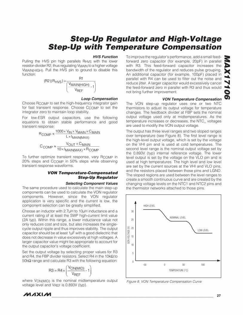
The output has three level ranges and two sloped ranges over temperature (see Figure 8). The first level range is the high-level output voltage, which is set by the voltage on the VHI pin and is used at cold temperatures. The second level range is the nominal output voltage set by the 0.893V (typ) internal reference voltage. The lower level output is set by the voltage on the VLO pin and is used at high temperatures. The high level and low level are set by the current sources at the VHI and VLO pins, and the resistors placed between those pins and LGND. The sloped regions are used between the level ranges to create a smooth continuous curve and are created by the changing voltage levels on the NTC1 and NTC2 pins and the thermistor networks attached to those pins.
Figure 8. VON Temperature Compensation Curve
TEMPERATURE (NC)
-50 0 50 100
30
25
20
15
10
5
0
GON
VOLT
AGE
(V)
HIGH LEVEL
LOW LEVEL
NOMINAL LEVEL
Step-Up Regulator and High-Voltage Step-Up with Temperature Compensation
MA
X1
71
06
28 _____________________________________________________________________________________
The VHI voltage is used as the reference for FBP whenever the voltage on NTC1 is greater than the voltage on VHI. The curve between the high-level range and the nominal-level range is determined directly by the voltage on the thermistor network at the NTC1 pin, which is used whenever the NTC1 pin voltage is both greater than the nominal internal reference voltage and less than the VHI voltage. The nominal reference voltage is used whenever the NTC1 voltage is less than the nominal reference. The curve between the nominal-level range and the low-level range is determined directly by the voltage on the thermistor network at the NTC2 pin, and is used whenever the NTC2 pin voltage is both less than the nominal FBP reference voltage and greater than the VLO voltage and NTC1 is also less than the nominal FBP reference level. The VLO voltage is used as the reference whenever the NTC2 voltage is less than the VLO voltage and the NTC1 voltage is less than the nominal reference voltage.
This can be described in a logic language as follows:
Feedback Reference = IF (VNTC1 > VVHI) THEN use VHIELSE IF (VNTC1 > REF) THEN use VNTC1ELSE IF (VNTC2>REF) THEN use REFELSE IF (VNTC2 > VVLO) THEN use VNTC2ELSE use VLO
where REF is the internal 0.893V reference.
The result is that, with the proper external components, the FBP voltage level varies smoothly over temperature from VHI at low temperatures to VLO at high temperatures. The external components can be selected to adjust these levels and at what temperatures these transitions occur.
The high level and low level are set by the current sources at VHI and VLO, and the resistors placed there to LGND:
HI VHI VHI
LO VLO VLO
V I R
V I R
= ×
= ×
where IVLO is the source current from the VLO pin and IVHI is the source current from the VHI pin.
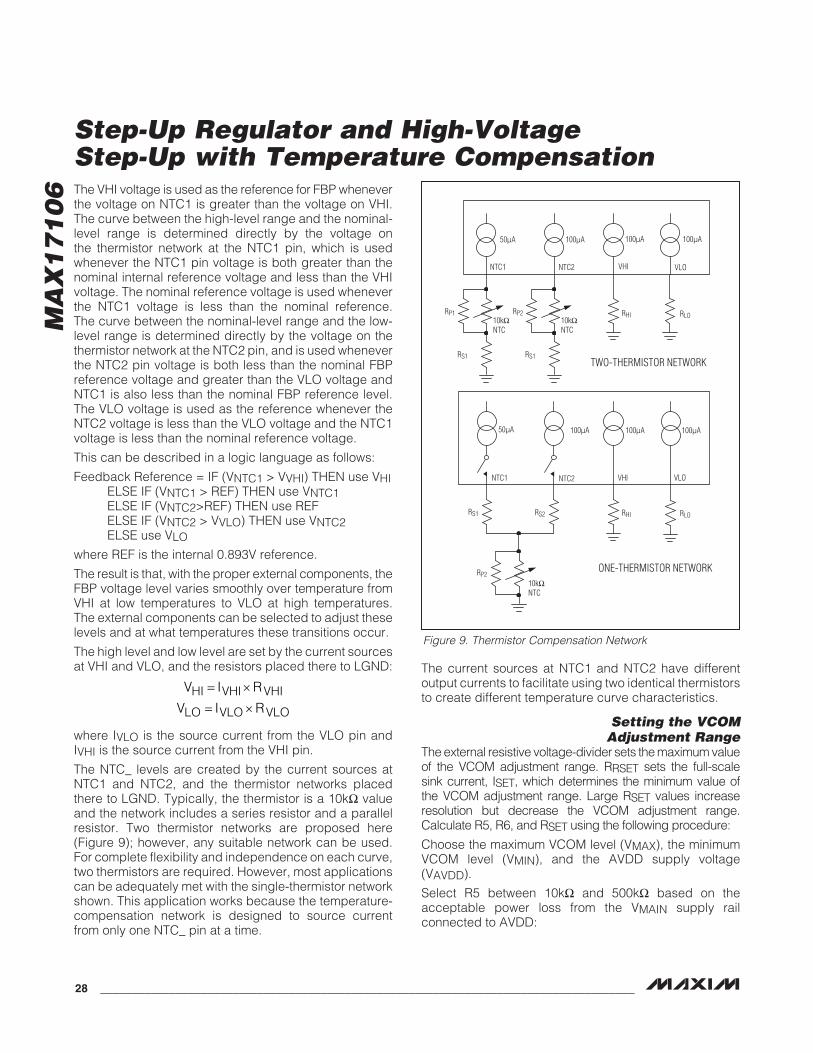
The NTC_ levels are created by the current sources at NTC1 and NTC2, and the thermistor networks placed there to LGND. Typically, the thermistor is a 10kI value and the network includes a series resistor and a parallel resistor. Two thermistor networks are proposed here (Figure 9); however, any suitable network can be used. For complete flexibility and independence on each curve, two thermistors are required. However, most applications can be adequately met with the single-thermistor network shown. This application works because the temperature- compensation network is designed to source current from only one NTC_ pin at a time.
The current sources at NTC1 and NTC2 have different output currents to facilitate using two identical thermistors to create different temperature curve characteristics.
Setting the VCOM Adjustment Range
The external resistive voltage-divider sets the maximum value of the VCOM adjustment range. RRSET sets the full-scale sink current, ISET, which determines the minimum value of the VCOM adjustment range. Large RSET values increase resolution but decrease the VCOM adjustment range. Calculate R5, R6, and RSET using the following procedure:
Choose the maximum VCOM level (VMAX), the minimum VCOM level (VMIN), and the AVDD supply voltage (VAVDD).
Select R5 between 10kI and 500kI based on the acceptable power loss from the VMAIN supply rail connected to AVDD:
Figure 9. Thermistor Compensation Network
50FA
RP1
RS1
10kINTC
100FA
VHI VLONTC1
100FA
RP2
RS1
NTC2
50FA
RS1
VHI VLONTC1
100FA
RS2
NTC2
TWO-THERMISTOR NETWORK
ONE-THERMISTOR NETWORK
100FA
100FA 100FA
RHI RLO
RHI RLO
10kINTC
RP210kINTC
Step-Up Regulator and High-Voltage Step-Up with Temperature Compensation
MA
X1
71
06
______________________________________________________________________________________ 29
1) Calculate R6:
MAX
MAX
VR6 R5
AVDD-V≅ ×
2) Calculate RSET:
SETMAX MIN
AVDD R5//R6R
20 V - V= ×
3) Verify that ISET does not exceed 120FA:
AVDDSET
SET
VI
20 R=
×
If ISET exceeds 120FA, return to step 2 and choose a larger value for R5.
The resulting resolution is:
MAX MIN(V - V )127
A complete design example is given below:
VMAX = 4V, VMIN = 2.4V, VMAIN = 8V
If R5 = 200kI, then R6 = 200kI and RSET = 25kI.
Resolution = 12.6mV
Fault ProtectionIf FB or FBP is lower than 0.1V, the relative step-up regulator is disabled. If FB or FBP is continuously below 80% of its regulation level for more than 50ms (typ), all three outputs (VMAIN, VON, and VLOUT) are disabled for 160ms and then go through a full soft-start process. If the fault remains, this process repeats up to three times. After the final shutdown, the fault condition is latched. Recycle the power to start the part again.
Applications InformationPower Dissipation
An IC’s maximum power dissipation depends on the thermal resistance from the die to the ambient environment and the ambient temperature. The thermal resistance depends on the IC package, PCB copper area, other thermal mass, and airflow.
The 7mm x 7mm, 56-pin TQFN package can dissipate 2400mW (derated 40mW/NC above +70NC) for a single-layer board. More PCB copper, cooler ambient air, and more airflow increase the possible dissipation, while less copper or warmer air decreases the IC’s dissipation capability. The major components of power dissipation are the power dissipated in the two step-up regulators, the operational amplifiers, and the high-voltage scan-driver outputs.
Main Step-Up RegulatorThe largest portions of the power dissipated by the step-up regulator are the internal the MOSFET. It includes conduction loss and switching loss. The worst-case conduction loss occurs when the device is operating from the lowest expected input voltage, with the highest regulation output voltage, and at the maximum output current allowed by the current limit of the SW switch. The conduction loss can be estimated as:
22 RIPPLE
CONDUCTION(MAIN) IN SWI
PD (I ) D R12
= + × ×
where:
MAIN DIODEIN MAIN
IN SW
V VI I
V - V+
= ×
is the input current:
MAIN DIODE IN
MAIN DIODE SW
V V - VD
V V - V+
=+
is the duty factor, VDIODE is the voltage drop across diode, VSW is the voltage drop across MOSFET. RSW is the MOSFET on-resistance. IRIPPLE is inductor ripple current, which is usually small compared to IIN and thus can be ignored.
Assuming normal operation with VIN = 3V, VMAIN = 8V, IMAIN = 300mA, fSW = 1.2MHz, L1 = 3.6FH, RSW = 240mI, VDIODE = 0.5V, VSW = 240mV, the total conduction loss is PDCONDUCTION(MAIN) = 140mW.
The switching loss can be estimated as:
RSW FSWSWITCH(MAIN) MAIN IN SW
t tPD V I f
2+
= × × ×
where tRSW is switching node rising time and tFSW is switching node falling time. If tR = tF = 15ns, the switching loss is PDSWITCH = 134mW.
Operational AmplifiersThe power dissipated in the operational amplifiers depends on the output current, the output voltage, and the supply voltage:
( )SOURCE VCOM(SOURCE) AVDD COM
SINK VCOM(SINK) COM
PD I V - V
PD I V
= ×
= ×
where VAVDD is the supply voltage, IVCOM(SOURCE) is the output current sourced by one operational amplifier, and IVCOM(SINK) is the output current that the operational amplifier sinks.
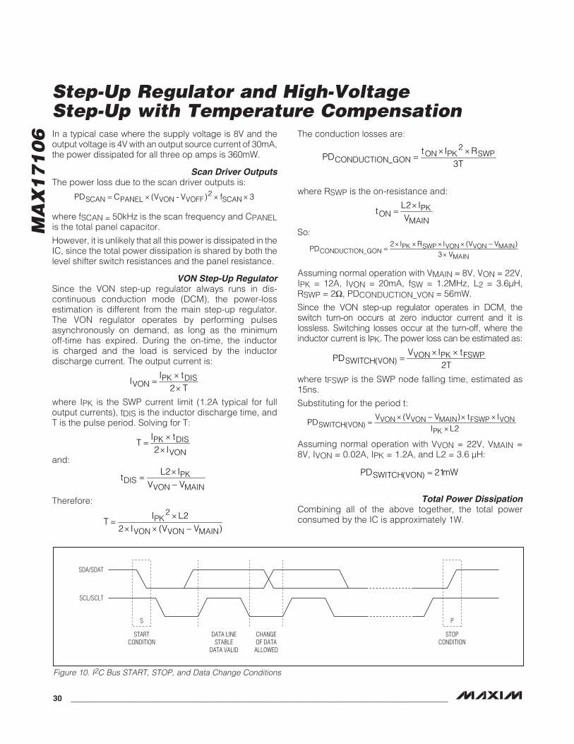
Step-Up Regulator and High-Voltage Step-Up with Temperature Compensation
MA
X1
71
06
30 _____________________________________________________________________________________
In a typical case where the supply voltage is 8V and the output voltage is 4V with an output source current of 30mA, the power dissipated for all three op amps is 360mW.
Scan Driver OutputsThe power loss due to the scan driver outputs is:
2SCAN PANEL VON VOFF SCANPD C (V - V ) f 3= × × ×
where fSCAN = 50kHz is the scan frequency and CPANEL is the total panel capacitor.
However, it is unlikely that all this power is dissipated in the IC, since the total power dissipation is shared by both the level shifter switch resistances and the panel resistance.
VON Step-Up RegulatorSince the VON step-up regulator always runs in dis-continuous conduction mode (DCM), the power-loss estimation is different from the main step-up regulator. The VON regulator operates by performing pulses asynchronously on demand, as long as the minimum off-time has expired. During the on-time, the inductor is charged and the load is serviced by the inductor discharge current. The output current is:
where IPK is the SWP current limit (1.2A typical for full output currents), tDIS is the inductor discharge time, and T is the pulse period. Solving for T:
and:
Therefore:
The conduction losses are:
where RSWP is the on-resistance and:
So:
Assuming normal operation with VMAIN = 8V, VON = 22V, IPK = 12A, IVON = 20mA, fSW = 1.2MHz, L2 = 3.6FH, RSWP = 2I, PDCONDUCTION_VON = 56mW.
Since the VON step-up regulator operates in DCM, the switch turn-on occurs at zero inductor current and it is lossless. Switching losses occur at the turn-off, where the inductor current is IPK. The power loss can be estimated as:
where tFSWP is the SWP node falling time, estimated as 15ns.
Substituting for the period t:
Assuming normal operation with VVON = 22V, VMAIN = 8V, IVON = 0.02A, IPK = 1.2A, and L2 = 3.6 µH:
Total Power DissipationCombining all of the above together, the total power consumed by the IC is approximately 1W.
Figure 10. I2C Bus START, STOP, and Data Change Conditions
PK DISVON
I tI
2 T×
=×
PK DIS
VON
I tT
2 I×
=×
PKDIS
VON MAIN
L2 It
V V×
=−
2PK
VON VON MAIN
I L2T
2 I (V V )×
=× × −
2ON PK SWP
CONDUCTION_GONt I R
PD3T
× ×=
PKON
MAIN
L2 It
V×
=
PK SWP VON VON MAINCONDUCTION_GON
MAIN
2 I R I (V V )PD
3 V× × × × −
=×
VON PK FSWPSWITCH(VON)
V I tPD
2T× ×
=
VON VON MAIN FSWP VONSWITCH(VON)
PK
V (V V ) t IPD
I L2× − × ×
=×
SWITCH(VON)PD 21mW=
SDA/SDAT
SCL/SCLT
S
STARTCONDITION
STOPCONDITION
DATA LINESTABLE
DATA VALID
CHANGEOF DATAALLOWED
P
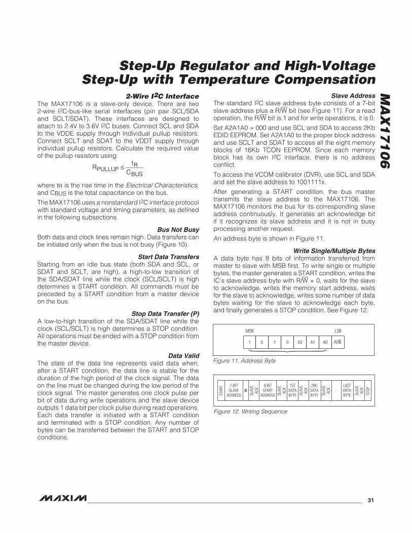
Step-Up Regulator and High-Voltage Step-Up with Temperature Compensation
MA
X1
71
06
______________________________________________________________________________________ 31
2-Wire I2C InterfaceThe MAX17106 is a slave-only device. There are two 2-wire I2C-bus-like serial interfaces (pin pair SCL/SDA and SCLT/SDAT). These interfaces are designed to attach to 2.4V to 3.6V I2C buses. Connect SCL and SDA to the VDDE supply through individual pullup resistors. Connect SCLT and SDAT to the VDDT supply through individual pullup resistors. Calculate the required value of the pullup resistors using:
RPULLUP
BUS
tR
C≤
where tR is the rise time in the Electrical Characteristics, and CBUS is the total capacitance on the bus.
The MAX17106 uses a nonstandard I2C interface protocol with standard voltage and timing parameters, as defined in the following subsections.
Bus Not BusyBoth data and clock lines remain high. Data transfers can be initiated only when the bus is not busy (Figure 10).
Start Data TransfersStarting from an idle bus state (both SDA and SCL, or SDAT and SCLT, are high), a high-to-low transition of the SDA/SDAT line while the clock (SCL/SCLT) is high determines a START condition. All commands must be preceded by a START condition from a master device on the bus.
Stop Data Transfer (P)A low-to-high transition of the SDA/SDAT line while the clock (SCL/SCLT) is high determines a STOP condition. All operations must be ended with a STOP condition from the master device.
Data ValidThe state of the data line represents valid data when, after a START condition, the data line is stable for the duration of the high period of the clock signal. The data on the line must be changed during the low period of the clock signal. The master generates one clock pulse per bit of data during write operations and the slave device outputs 1 data bit per clock pulse during read operations. Each data transfer is initiated with a START condition and terminated with a STOP condition. Any number of bytes can be transferred between the START and STOP conditions.
Slave AddressThe standard I2C slave address byte consists of a 7-bit slave address plus a R/W bit (see Figure 11). For a read operation, the R/W bit is 1 and for write operations, it is 0.
Set A2A1A0 = 000 and use SCL and SDA to access 2Kb EDID EEPROM. Set A2A1A0 to the proper block address and use SCLT and SDAT to access all the eight memory blocks of 16Kb TCON EEPROM. Since each memory block has its own I2C interface, there is no address conflict.
To access the VCOM calibrator (DVR), use SCL and SDA and set the slave address to 1001111x.
After generating a START condition, the bus master transmits the slave address to the MAX17106. The MAX17106 monitors the bus for its corresponding slave address continuously. It generates an acknowledge bit if it recognizes its slave address and it is not in busy processing another request.
An address byte is shown in Figure 11.
Write Single/Multiple BytesA data byte has 8 bits of information transferred from master to slave with MSB first. To write single or multiple bytes, the master generates a START condition, writes the IC’s slave address byte with R/W = 0, waits for the slave to acknowledge, writes the memory start address, waits for the slave to acknowledge, writes some number of data bytes waiting for the slave to acknowledge each byte, and finally generates a STOP condition. See Figure 12.
Figure 11. Address Byte
Figure 12. Writing Sequence
1 0
MSB LSB
1 0 A2 A1 A0 R/W
STAR
T
STOP0
SLAV
EAC
K
SLAV
EAC
K
SLAV
EAC
K
SLAV
EAC
K
SLAV
EAC
K. . .7-BIT
SLAVEADDRESS
8-BITSTART
ADDRESS
1STDATABYTE
2NDDATABYTE
LASTDATABYTE
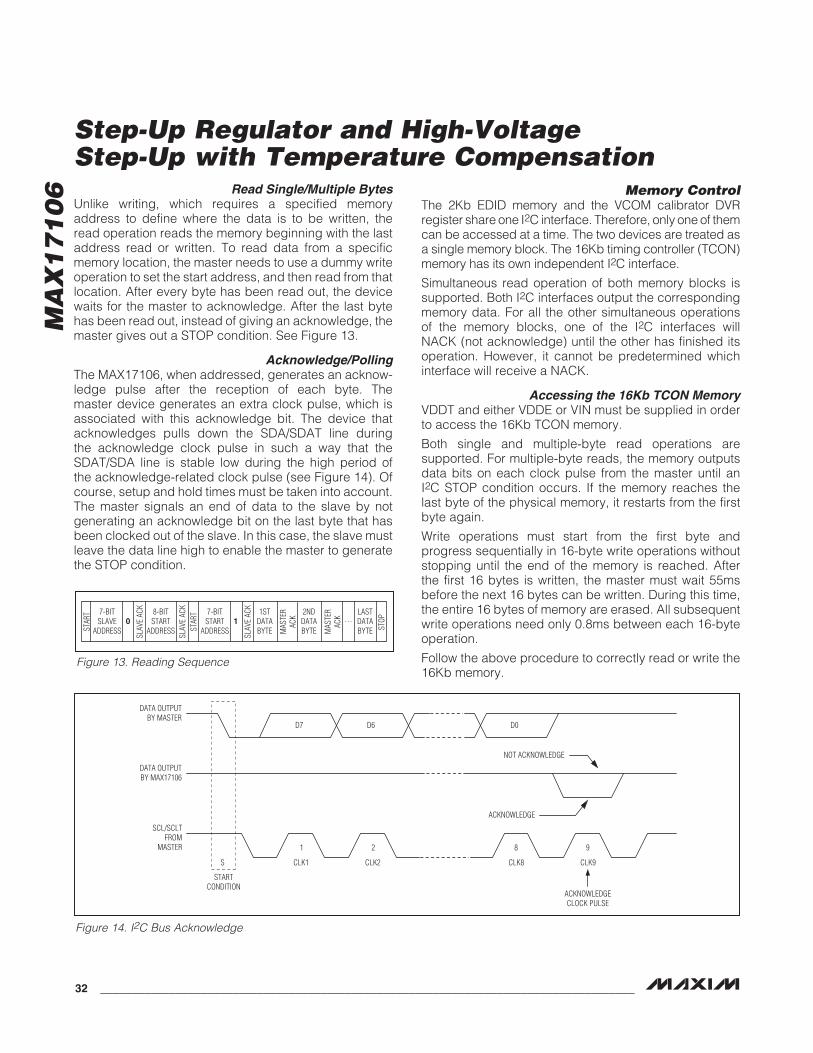
Step-Up Regulator and High-Voltage Step-Up with Temperature Compensation
MA
X1
71
06
32 _____________________________________________________________________________________
Read Single/Multiple BytesUnlike writing, which requires a specified memory address to define where the data is to be written, the read operation reads the memory beginning with the last address read or written. To read data from a specific memory location, the master needs to use a dummy write operation to set the start address, and then read from that location. After every byte has been read out, the device waits for the master to acknowledge. After the last byte has been read out, instead of giving an acknowledge, the master gives out a STOP condition. See Figure 13.
Acknowledge/PollingThe MAX17106, when addressed, generates an acknow-ledge pulse after the reception of each byte. The master device generates an extra clock pulse, which is associated with this acknowledge bit. The device that acknowledges pulls down the SDA/SDAT line during the acknowledge clock pulse in such a way that the SDAT/SDA line is stable low during the high period of the acknowledge-related clock pulse (see Figure 14). Of course, setup and hold times must be taken into account. The master signals an end of data to the slave by not generating an acknowledge bit on the last byte that has been clocked out of the slave. In this case, the slave must leave the data line high to enable the master to generate the STOP condition.
Memory ControlThe 2Kb EDID memory and the VCOM calibrator DVR register share one I2C interface. Therefore, only one of them can be accessed at a time. The two devices are treated as a single memory block. The 16Kb timing controller (TCON) memory has its own independent I2C interface.
Simultaneous read operation of both memory blocks is supported. Both I2C interfaces output the corresponding memory data. For all the other simultaneous operations of the memory blocks, one of the I2C interfaces will NACK (not acknowledge) until the other has finished its operation. However, it cannot be predetermined which interface will receive a NACK.
Accessing the 16Kb TCON MemoryVDDT and either VDDE or VIN must be supplied in order to access the 16Kb TCON memory.
Both single and multiple-byte read operations are supported. For multiple-byte reads, the memory outputs data bits on each clock pulse from the master until an I2C STOP condition occurs. If the memory reaches the last byte of the physical memory, it restarts from the first byte again.
Write operations must start from the first byte and progress sequentially in 16-byte write operations without stopping until the end of the memory is reached. After the first 16 bytes is written, the master must wait 55ms before the next 16 bytes can be written. During this time, the entire 16 bytes of memory are erased. All subsequent write operations need only 0.8ms between each 16-byte operation.
Follow the above procedure to correctly read or write the 16Kb memory.
Figure 14. I2C Bus Acknowledge
Figure 13. Reading Sequence
SCL/SCLT FROM
MASTER
DATA OUTPUTBY MAX17106
DATA OUTPUTBY MASTER
CLK1
STARTCONDITION
S
1
CLK2
2
CLK8
8
CLK9
9
ACKNOWLEDGECLOCK PULSE
ACKNOWLEDGE
NOT ACKNOWLEDGE
D7 D6 D0
STAR
T
STAR
T
STOP0 1
SLAV
E AC
K
SLAV
E AC
K
SLAV
E AC
K
MAS
TER
ACK
MAS
TER
ACK . . .
7-BITSLAVE
ADDRESS
8-BITSTART
ADDRESS
7-BITSTART
ADDRESS
1STDATABYTE
2NDDATABYTE
LASTDATABYTE

Step-Up Regulator and High-Voltage Step-Up with Temperature Compensation
MA
X1
71
06
______________________________________________________________________________________ 33
Accessing the 2Kb EDID MemoryVDDE must be supplied to access the 2Kb EDID memory.
Both single- and multiple-byte read operations are sup-ported. For multiple-byte reads, the memory outputs data bits on each clock pulse from the master until an I2C stop occurs. If the memory reaches the last byte of the physical memory, it restarts from the first byte again.
Write operations must start from the first byte and progress sequentially in either 1-byte or 8-byte operations without stopping until the end of the memory is reached. Once starting with a single-byte write operation, the complete memory must be written in single-byte operations. Similarly, once starting with an 8-byte write operation, the complete memory must be written in 8-byte operations. Switching between 1-byte and 8-byte operations is not supported.
After the first single-byte or 8-byte write operation, the master must wait 55ms before the following write operation. During this time, the entire 16Kb of memory are erased. All subsequent write operations need only 0.5ms between each write operation
Follow the above procedure to correctly read or write the 16Kb memory.
Accessing the VCOM Calibrator DVR 7-Bit Register
The VCOM calibrator register contains both a volatile register (VR) and nonvolatile register (NVR). The volatile register controls the VCOM calibrator operation. The nonvolatile register is automatically copied to the volatile register at power-up to set the VCOM output voltage.
VDDE must be present to access the nonvolatile register. When writing to the VCOM calibrator, the calibrator data byte contains a 7-bit setting and a program bit (LSB). If the program bit is 1, the data is written only into the volatile register. If the program bit is 0, the data is written into both the volatile and nonvolatile registers. For read operations, the program bit is a don’t-care bit. WPN must be high to write to either the volatile or nonvolatile registers.
Read operations to the VCOM calibrator return the data stored in the nonvolatile register. Read operations can be performed whether WPN is low or high.
Table 5 lists the DAC values and the corresponding ISET, VSET, and VOUT values.
PCB Layout and GroundingCareful PCB layout is important for proper operation. Use the following guidelines for good PCB layout:
U Minimize the area of high-current loops by placing the inductor, output diode, and output capacitors near the input capacitors and near the SW (SWP) and PGND pins. The high-current input loop goes from the positive terminal of the input capacitor to the inductor, to the IC’s SW (SWP) pin, out of PGND, and to the input capacitor’s negative terminal. The high-current output loop is from the positive terminal of the input capacitor to the inductor, to the output diode D1 (D2), to the positive terminal of the output capacitors, reconnecting between the output capacitor and input capacitor ground terminals. Connect these loop components with short, wide connections. Avoid using vias in the high-current paths. If vias are unavoidable, try to use them only in the loop segments that have continuous current (not switched currents) and use many vias in parallel to reduce resistance and inductance. For a step-up converter, the segment between the input capacitor and the inductor has continuous current.
Table 5. DAC Settings
7-BITDATA BYTE
IRSET VRSET (V) VCOMX (V)
1111111 IRSET(MAX) VRSET(MAX) VMIN
1111110IRSET(MAX) -
1 LSBVRSET(MAX) -
1 LSBVMIN +1 LSB
.
.
.
.
.
.
.
.
.
.
.
.
00000001IRSET(MIN) +
1 LSBVRSET(MIN) +
1 LSBVMAX - 1 LSB
00000000 IRSET(MIN) VRSET(MIN) VMAX
Step-Up Regulator and High-Voltage Step-Up with Temperature Compensation
MA
X1
71
06
34 _____________________________________________________________________________________
U Create a power ground island for the main step-up converter consisting of the input and output capacitor grounds, PGND pins (45, 46) and any charge-pump component grounds. Connect all these together with short, wide traces or a small ground plane. Maximizing the width of the power ground traces improves efficiency and reduces output voltage ripple and noise spikes. Create a second power ground island for the VON step-up converter consisting of the input and output capacitor grounds and the PGND pin (56). Connect these together with short, wide traces or a small ground plane. Since the VON step-up’s input capacitor is in parallel with the main step-up’s output capacitor, connect these two PGND islands together with a wide trace between these capacitor grounds or make it one big island or ground plane.
U Create an analog ground plane (LGND) consisting of the LGND pin, all the feedback-divider ground connections, the operational amplifier divider ground connections, the COMP capacitor ground connection, the AVDD capacitor ground connection, and the device’s exposed backside pad. Connect the LGND island to the two PGND islands by connecting only one PGND pin (45) directly to the exposed backside pad. Make no other connections between these separate ground planes. Multiple connections cause PGND currents to pass through and disturb the LGND ground plane.
U Place the feedback-voltage-divider resistors as close as possible to the feedback pin. The divider’s center trace should be kept short. Placing the resistors far away causes the feedback traces to become an antenna that can pick up switching noise. Care should be taken to avoid running a feedback trace near any step-up or charge-pump switching nodes.
U Place the VIN pin bypass capacitor as close as possible to the device. The ground connections of the VIN bypass capacitor should be connected directly to the LGND pin or the backside pad with a wide trace.
U Minimize the length and maximize the width of the traces between the output capacitors and the load for best transient responses.
U Minimize the size of the step-up converter switching nodes while keeping them wide and short. Keep these nodes away from the feedback node and analog ground. Use DC traces as shields if necessary.
Refer to the MAX17106 evaluation kit for an example of proper board layout.
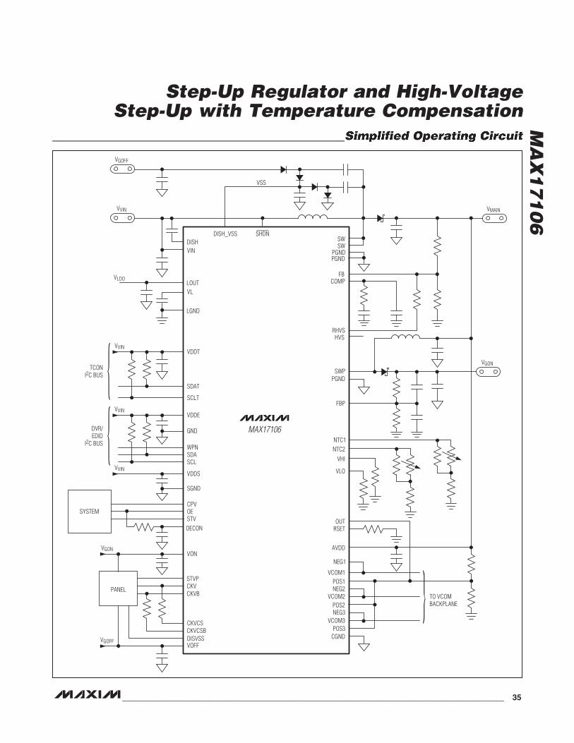
Step-Up Regulator and High-Voltage Step-Up with Temperature Compensation
MA
X1
71
06
______________________________________________________________________________________ 35
Simplified Operating Circuit
VGOFF
VMAIN
TO VCOMBACKPLANE
COMP
SW
PGND
CGND
VCOM2POS2
NEG2
FB
AVDD
VIN
RSET
SHDN
OECON
STV
DISH
OECPV
OUT
SYSTEM
PANEL
VCOM3POS3
NEG3
VCOM1
POS1
NEG1
STVPCKVCKVB
VOFF
CKVCSCKVCSB
HVSRHVS
SWP
FBP
SDAT
SCLT
TCONI2C BUS
DISH_VSS
DISVSS
PGND
SWPGND
NTC1
NTC2
VHI
VLO
VDDT
VLLOUT
LGND
VSS
VVIN
VLDO
VGON
VVIN
SDASCL
DVR/EDID
I2C BUSWPN
VDDE
GND
VVIN
VDDS
SGND
VVIN
VONVGON
VGOFF
MAX17106
Step-Up Regulator and High-Voltage Step-Up with Temperature Compensation
MA
X1
71
06
Maxim cannot assume responsibility for use of any circuitry other than circuitry entirely embodied in a Maxim product. No circuit patent licenses are implied. Maxim reserves the right to change the circuitry and specifications without notice at any time.
36 Maxim Integrated Products, 120 San Gabriel Drive, Sunnyvale, CA 94086 408-737-7600© 2009 Maxim Integrated Products Maxim is a registered trademark of Maxim Integrated Products, Inc.
Package InformationFor the latest package outline information and land patterns, go to www.maxim-ic.com/packages.
Chip InformationPROCESS: BiCMOS
PACKAGE TYPE PACKAGE CODE DOCUMENT NO.
56 TQFN T5677MN+1 21-0144