0.5a step-down switching regulator
TRANSCRIPT

TC2574-2 12/22/00
TC2574
© 2001 Microchip Technology Inc. DS21397A
0.5A Step-Down Switching Regulator
GENERAL DESCRIPTION
The TC2574 series of regulators are monolithic inte-grated circuits ideally suited for easy and convenient designof a step-down switching regulator (buck converter). Allcircuits of this series are capable of driving a 0.5A load withexcellent line and load regulation. These devices are avail-able in fixed output voltages of 3.3V, 5.0V, 12V andan adjustable output version.
These regulators were designed to minimize the num-ber of external components to simplify the power supplydesign. Standard series of inductors optimized for use withthe TC2574 are offered by several different inductor manu-facturers.
Since the TC2574 converter is a switch–mode powersupply, its efficiency is significantly higher in comparisonwith popular three-terminal linear regulators, especially withhigher input voltages. In most cases, the power dissipatedby the TC2574 regulator is so low, that the copper traces onthe printed circuit board are normally the only heatsinkneeded and no additional heatsinking is required.
The TC2574 features include a guaranteed ±4% toler-ance on output voltage within specified input voltages andoutput load conditions, and ±10% on the oscillator frequency(±2% over 0°C to +125°C). External shutdown is included,featuring 60µA (typical) standby current. The output switchincludes cycle–by–cycle current limiting, as well as thermalshutdown for full protection under fault conditions.
FEATURES
3.3V, 5.0V, 12V and Adjustable Output Versions Adjustable Version Output Voltage Range,
1.23 to 37 V ±4% Max Over Line and Load Conditions Guaranteed 0.5 A Output Current Wide Input Voltage Range: 4.75 to 40V Requires Only 4 External Components 52kHz Fixed Frequency Internal Oscillator TTL Shutdown Capability, Low Power Standby Mode High Efficiency Uses Readily Available Standard Inductors Thermal Shutdown and Current Limit Protection
APPLICATIONS
Simple and High–Efficiency Step–Down (Buck)Regulator
Efficient Pre-Regulator for Linear Regulators On–Card Switching Regulators Positive to Negative Converters (Buck–Boost) Negative Step-Up Converters Power Supply for Battery Chargers
ORDERING INFORMATIONPart TemperatureNumber Package Range
TC2574-3.3VPA 8-Pin PDIP (Narrow) –40 to +125°CTC2574-5.0VPA 8-Pin PDIP (Narrow) –40 to +125°CTC2574-12.0VPA 8-Pin PDIP (Narrow) –40 to +125°CTC2574-VPA* 8-Pin PDIP (Narrow) –40 to +125°CTC2574-VOE* 16-Pin SOIC (Wide) –40 to +125°C
PIN CONFIGURATIONS
1
2
3
4
16
15
14
13SIG GND
5
6
7
12
11
10
98
FB
NC
NC
OUTPUT
TC2574
NC
NC
NC
NC
NC
NC
NC
NC
PWR GND
ON/OFF
1 8
2 7
3 6
4 5
SIG GND
FB
OUTPUT
VIN
VIN
NC
NC
PWR GND
TC2574ON/OFF
16-Pin SOIC (Wide)
8-Pin PDIP (Narrow)Note: *ADJ = 1.23 To 37V.

TC2574
2TC2574-2 12/22/00
0.5A Step-Down Switching Regulator
© 2001 Microchip Technology Inc. DS21397A
ABSOLUTE MAXIMUM RATINGS*
Maximum Supply Voltage ................................ VIN = 45VON/OFF Pin Input Voltage ..................... –0.3V ≤ V ≤ +VINOutput Voltage to Ground (Steady State) ...............–1.0 VMax Power Dissipation (SOIC) ........... (Internally Limited)
Thermal Resistance, Junction-to-Ambient ..... 145°C/WMax Power Dissipation (PDIP) ............ (Internally Limited)
Thermal Resistance, Junction-to-Ambient ... 100°C/WThermal Resistance, Junction-to-Case ........ 5.0°C/W
Storage Temperature Range ................. –65°C to +150°C
Minimum ESD Rating .............................................. 2.0kV(Human Body Model: C = 100 pF, R = 1.5 kΩ)
Lead Temperature (Soldering, 10 seconds).......... 260 °CMaximum Junction Temperature............................. 150°COperating Junction Temperature Range .... –40 to +125*CSupply Voltage ............................................................40V *This is a stress rating only, and functional operation of the device at theseor any other conditions beyond those indicated in the operation section ofthe specifications is not implied. Exposure to absolute maximum ratingsconditions for extended periods of time may affect device reliability.
ELECTRICAL CHARACTERISTICS: Unless otherwise specified, VIN = 12V for the 3.3V, 5.0V, and Adjustableversion,VIN = 25V for the 12V version. ILOAD = 100mA. For typical values TJ = 25°C, for min/max values TJ is the operatingjunction temperature range that applies (Note 2), unless otherwise noted.
Symbol Parameter Test Conditions Min Typ Max Units
TC2574-3.3 [( Note 1) Test Circuit Figure 2]VOUT Output Voltage VIN = 12V, ILOAD = 100mA, TJ = 25°C 3.234 3.3 3.366 V
4.75V ≤ VIN ≤ 40V, 0.1A ≤ ILOAD ≤ 0.5AVTJ = 25°C 3.168 3.3 3.432TJ = –40°C to +125° 3.135 — 3.465
η Efficiency VIN = 12V, ILOAD = 0.5 A — 72 — %
TC2574-5 [( Note 1) Test Circuit Figure 2]VOUT Output Voltage VIN = 12V, ILOAD = 100mA, TJ = 25°C 4.9 5.0 5.1 V
7.0V ≤ VIN ≤ 40V, 0.1A ≤ ILOAD ≤ 0.5ATJ = 25°C 4.8 5.0 5.2TJ = –40°C to +125°C 4.75 — 5.25
η Efficiency VIN = 12V, ILOAD = 0.5 A — 77 — %
TC2574-12 [( Note 1) Test Circuit Figure 2]VOUT Output Voltage VIN = 25V, ILOAD = 100mA, TJ = 25°C 11.76 10 12.24 V
15V ≤ VIN ≤ 40V, 0.1A ≤ ILOAD ≤ 0.5ATJ = 25°C 11.52 12 12.48TJ = –40°C to +125°C 11.4 — 12.6
η Efficiency VIN = 15V, ILOAD = 0.5 A — 88 — %
TC2574-Adjustable Version [( Note 1) Test Circuit Figure 2]VFB Feedback Voltage VIN = 12V, ILOAD = 100mA, VOUT = 5.0V, 1.217 1.23 1.243 V
TJ = 25*C
VFBT Feedback Voltage 7.0V ≤ VIN ≤ 40V, 0.1A ≤ ILOAD ≤ 0.5AVOUT = 5.0V
TJ = 25°C 1.193 1.23 1.267TJ = –40°C to +125°C 1.18 — 1.28
η Efficiency VIN = 12V, ILOAD = 0.5A, VOUT = 5.0V — 77 — %NOTES: 1. External components such as the catch diode, inductor, input and output capacitors can affect the switching regulator system
performance. When the TC2574 is used as shown in the Figure 2 test circuit, the system performance will be asshown in the system parameters section of the Electrical Characteristics.
2. Tested junction temperature range for the TC2574: TLOW = –40°C THIGH = +125°C

3
TC2574
0.5A Step-Down Switching Regulator
TC2574-2 12/22/00© 2001 Microchip Technology Inc. DS21397A
ELECTRICAL CHARACTERISTICS: Unless otherwise specified, VIN = 12V for the 3.3V, 5.0V, and Adjustableversion,VIN = 25V for the 12V version. ILOAD = 100mA. For typical values TJ = 25°C, for min/max values TJ is the operat-ing junction temperature range that applies (Note 2), unless otherwise noted.
Symbol Parameter Test Conditions Min Typ Max Units
TC2574-ADJUSTABLE VERSION [(Note 1) Test Circuit Figure 2]Ib Feedback Bias Current VOUT = 5.0V (Adjustable Version Only) nA
TJ = 25°C — 25 100TJ = –40°C to +125°C — — 200
fO Oscillator Frequency (Note 3) TJ = 25°C — 52 — kHzTJ = 0 to +125°C 47 52 58TJ = –40 to +125°C 42 – 63
VSAT Saturation Voltage IOUT = 0.5 A, (Note 4) VTJ = 25°C — 1.0 1.2TJ = –40 to +125°C — — 1.4
DC Max Duty Cycle (“on”) [Note 5] 93 98 — %
ICL Current Limit Peak Current (Notes 3 and 4) ATJ = 25°C 0.7 1.0 1.6TJ = –40 to +125°C 0.65 — 1.8
IL Output Leakage Current (Notes 6 and 7), TJ = 25°C mAOutput = 0 V — 0.6 2.0Output = – 1.0 V — 10 30
IQ Quiescent Current (Note 6) mATJ = 25°C — 5.0 9.0TJ = –40 to +125°C — — 11
ISTBY Standby Quiescent Current ON/OFF Pin = 5.0 V (“off”) µATJ = 25°C — 60 200TJ = –40 to +125°C — — 400
ON/OFF Pin Logic Input Level VVIH VOUT = 0V
TJ = 25°C 2.2 1.4 —TJ = –40 to +125°C 2.4 — —
VIL Nominal Output VoltageTJ = 25°C — 1.2 1.0TJ = –40 to +125°C — — 0.8
ON/OFF Pin Input Current mA µAIIH ON/OFF Pin = 5.0V (“off”), TJ = 25°C — 15 30
IIL ON/OFF Pin Input Current mA µAON/OFF Pin = 0 (“on”), TJ = 25°C — 0 5.0
NOTES: 1. External components such as the catch diode, inductor, input and output capacitors can affect the switching regulator systemperformance. When the TC2574 is used as shown in the Figure 2 test circuit, the system performance will be asshown in the system parameters section of the Electrical Characteristics.
2. Tested junction temperature range for the TC2574: TLOW = –40°C T high = +125°C3. The oscillator frequency reduces to approximately 18kHz in the event of an output short or an overload which causes the regulated
output voltage to drop approximately 40% from the nominal output voltage. This self protection feature lowers the average powerdissipation of the IC by lowering the minimum duty cycle from 5% down to approximately 2%.
4. Output (Pin 2) sourcing current. No diode, inductor or capacitor connected to the output pin.5. Feedback (Pin 4) removed from output and connected to 0 V.6. Feedback (Pin 4) removed from output and connected to 12V for the Adjustable, 3.3V, and 5.0V versions, and 25V for the 12V
version, to force the output transistor OFF.7. VIN = 40 V.

TC2574
4TC2574-2 12/22/00
0.5A Step-Down Switching Regulator
© 2001 Microchip Technology Inc. DS21397A
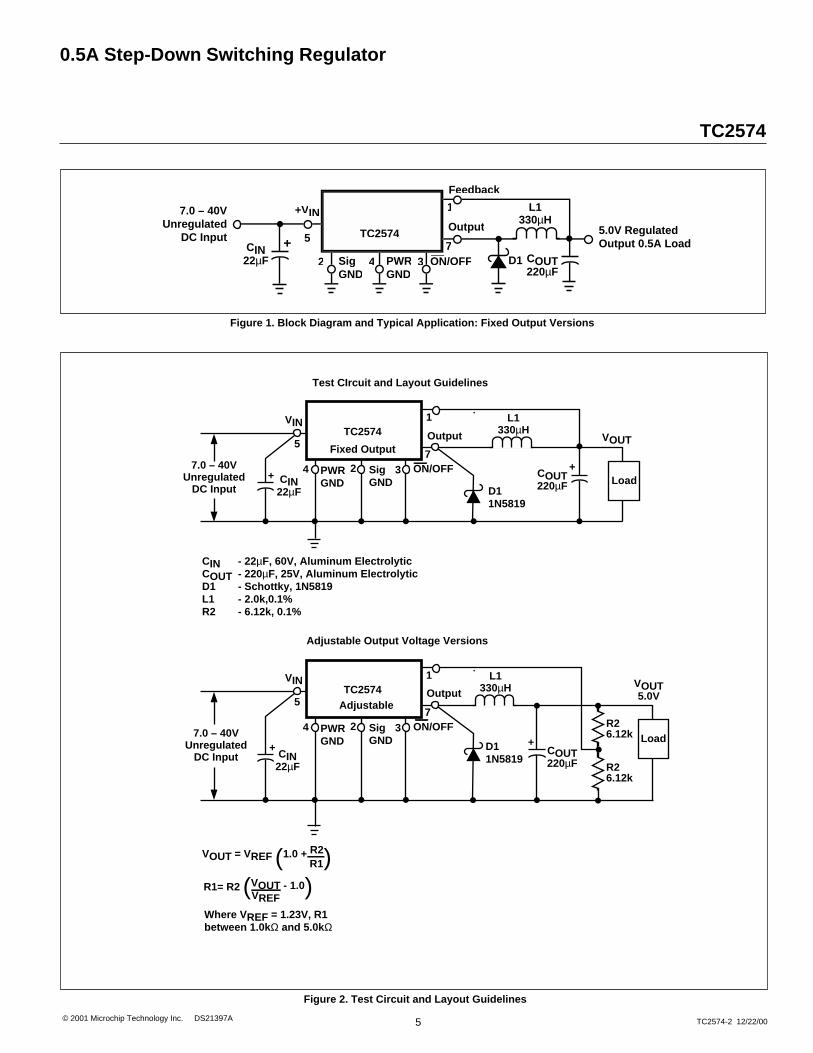
REPRESENTATIVE BLOCK DIAGRAM AND TYPICAL APPLICATION
PIN DESCRIPTION
Pin No. Pin No8-Pin PDIP 16-Pin SOIC Symbol Description
5 12 VIN This pin is the positive input supply for the TC2574 step–down switchingregulator. In order to minimize voltage transients and to supply the switchingcurrents needed by the regulator, a suitable input bypass capacitor must bepresent (CIN in Figure 1).
7 14 Output This is the emitter of the internal switch. The saturation voltage VSAT of thisoutput switch is typically 1.0V. It should be kept in mind that the PCB areaconnected to this pin should be kept to a minimum in order to minimizecoupling to sensitive circuitry.
2 4 SIG Gnd Circuit signal ground pin. See the information about the printed circuit boardlayout.
4 6 PWR GND Circuit power ground pin. See the information about the printed circuit boardlayout.
1 3 FB This pin senses regulated output voltage to complete the feedback loop. Thesignal is divided by the internal resistor divider network R2, R1 and applied tothe non–inverting input of the internal error amplifier.In the adjustable versionof the TC2574 switching regulator, this pin is the direct input of the erroramplifier and the resistor network R2, R1 is connected externally to allowprogramming of the output voltage.
3 5 ON/OFF It allows the switching regulator circuit to be shut down using logic levelsignals, thus dropping the total input supply current to approximately 80µA.The input threshold voltage is typically 1.5V. Applying a voltage above thisvalue (up to +VIN ) shuts the regulator off. If the voltage applied to this pin isower than 1.5 V or if this pin is left open, the regulator will be in the “on”condition.
TC2574
+
–
+
–
3.1V InternalRegulator ON/OFF
ON/OFF
LatchFreq.Shift
18kHz
Reset ThermalShutdown
3
71.0 AmpSwitch D1
L1
COUT
+VIN
CIN
VOUT
Driver
Output
PWR GND
1
5
2
For Adjustable versionR1 = open, R2 = 0Ω
Load
Feedback
UnregulatedDC Input
SIG GND
R1
R21.0k
CurrentLimit
Comparator
Fixed gainError Amplifier
+
+
+
–
52kHzOscillator
1.235VBand-GapReference 4
OutputVoltage Versions
3.3V5.0V12V
R2 (Ω)
1.7k3.1k8.84k
5
TC2574
0.5A Step-Down Switching Regulator
TC2574-2 12/22/00© 2001 Microchip Technology Inc. DS21397A
CIN22µF COUT
220µF
+VIN
5
2 SigGND
PWRGND
4 37
1 L1330µH
Output
D1
Feedback
ON/OFF
7.0 – 40VUnregulated
DC Input5.0V RegulatedOutput 0.5A Load
TC2574+
Figure 1. Block Diagram and Typical Application: Fixed Output Versions
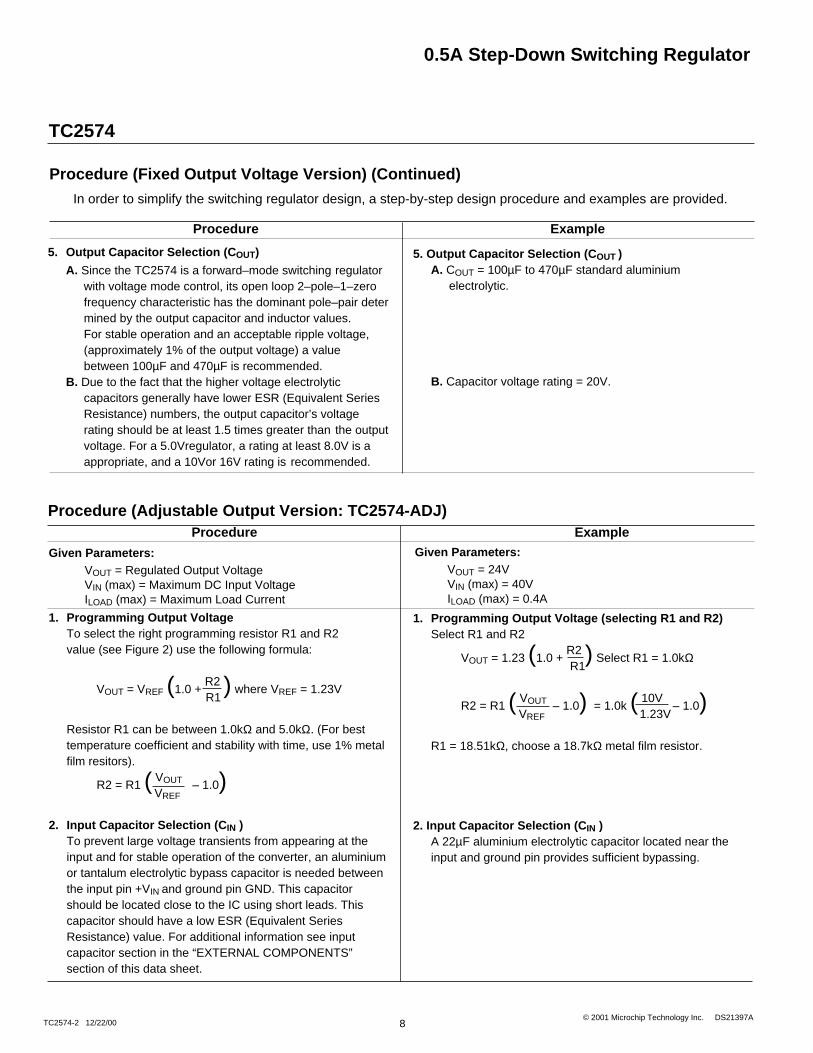
Figure 2. Test Circuit and Layout Guidelines
CIN22µF
COUT220µF
VOUT
VIN
5
4 SigGND
PWRGND
2 37
1
D11N5819
L1330µHOutput
Test CIrcuit and Layout Guidelines
CIN - 22µF, 60V, Aluminum ElectrolyticCOUT - 220µF, 25V, Aluminum ElectrolyticD1 - Schottky, 1N5819L1 - 2.0k,0.1%R2 - 6.12k, 0.1%
VOUT = VREF (1.0 + R2) R1
ON/OFF7.0 – 40VUnregulated
DC Input
TC2574
++
Load
Fixed Output
CIN22µF
R26.12k
R26.12k
COUT220µF
VOUT5.0V
VIN
5
4 SigGND
PWRGND
2 37
1
D11N5819
L1330µHOutput
Where VREF = 1.23V, R1between 1.0kΩ and 5.0kΩ
Adjustable Output Voltage Versions
ON/OFF7.0 – 40V
UnregulatedDC Input
TC2574
+ + Load
Adjustable
R1= R2 (VOUT - 1.0)VREF

TC2574
6TC2574-2 12/22/00
0.5A Step-Down Switching Regulator
© 2001 Microchip Technology Inc. DS21397A
PCB LAYOUT GUIIDELINES
As with any switching regulator, the layout of the printedcircuit board is very important. Rapidly switching currentsassociated with wiring inductance, stray capacitance andparasitic inductance of the printed circuit board traces cangenerate voltage transients which can generate electro-magnetic interferences (EMI) and affect the desired opera-tion. As indicated in the Figure 2, to minimize inductance andground loops, the length of the leads indicated by heavylines should be kept as short as possible.
For best results, single–point grounding (as indicated)or ground plane construction should be used.
On the other hand, the PCB area connected to thePin 7 (emitter of the internal switch) of the TC2574 shouldbe kept to a minimum in order to minimize coupling tosensitive circuitry.
Another sensitive part of the circuit is the feedback. It isimportant to keep the sensitive feedback wiring short. Toassure this, physically locate the programming resistorsnearto the regulator, when using the adjustable version ofthe TC2574 regulator.
DESIGN PROCEDURE
Buck Converter Basics
The TC2574 is a “Buck” or Step–Down Converter whichis the most elementary forward–mode converter. Its basicschematic can be seen in Figure 3.
The operation of this regulator topology has two distincttime periods. The first one occurs when the series switch ison, the input voltage is connected to the input of the inductor.
The output of the inductor is the output voltage, and therectifier (or catch diode) is reverse biased. During thisperiod, since there is a constant voltage source connectedacross the inductor, the inductor current begins to linearlyramp upwards, as described by the following equation:
IL (ON) = (VIN – VOUT ) tON
LDuring this “on” period, energy is stored within the core
material in the form of magnetic flux. If the inductor isproperly designed, there is sufficient energy stored to carrythe requirements of the load during the “off” period.
The next period is the “off” period of the power switch.When the power switch turns off, the voltage across theinductor reverses its polarity and is clamped at one diodevoltage drop below ground by the catch diode. Current nowflows through the catch diode thus maintaining the loadcurrent loop. This removes the stored energy from theinductor. The inductor current during this time is:
IL (OFF) = (VOUT – VD ) tOFF
LThis period ends when the power switch is once again
turned on. Regulation of the converter is accomplished byvarying the duty cycle of the power switch. It is possible todescribe the duty cycle as follows:
d = tON ,where T is the period of switching. T
For the buck converter with ideal components, the dutycycle can also be described as:
d = VOUT VIN
Figure 4 shows the buck converter idealized waveformsof the catch diode voltage and the inductor current.
Figure 3. Basic Buck Converter
COUT+ RLOAD
+
–
VIN D1
Power Switch LFigure 4. Buck Converter Idealized Waveforms
Time
VD/(FWD)
PowerSwitch
Off
PowerSwitch
Diode PowerSwitch
PowerSwitch
Off
VON (SW)
PowerSwitch
OnPowerSwitch
OnDio
de
Vo
ltag
e
Time
IMINDiode
ILOAD (AV)
IPK
Ind
uct
or
Cu
rren
t

7
TC2574
0.5A Step-Down Switching Regulator
TC2574-2 12/22/00© 2001 Microchip Technology Inc. DS21397A
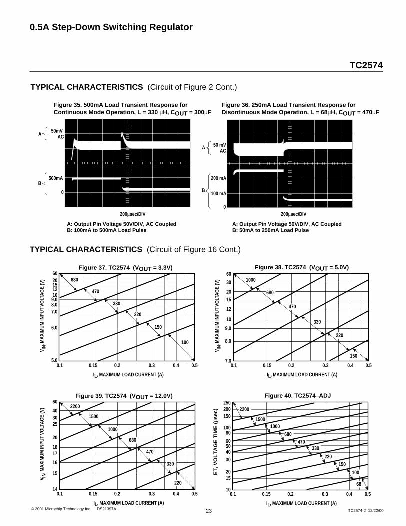
Procedure (Fixed Output Voltage Version)
In order to simplify the switching regulator design, a step-by-step design procedure and examples are provided.
Procedure ExampleGiven Parameters: Given Parameters:
VOUT = Regulated Output Voltage (3.3V, 5.0V or 12V) VOUT = 5.0 VVIN(max) = Maximum Input Voltage VIN (max) = 15 V
ILOAD(max) = Maximum Load Current ILOAD (max) = 0.4 A
1. Controller IC Selection 1. Controller IC SelectionAccording to the required input voltage, output voltage and According to the required input voltage, output voltage,current select the appropriate type of the controller polarity and current value, use the TC2574–5IC output voltage version. controlller IC.
2. Input Capacitor Selection (CIN ) 2. Input Capacitor Selection (CIN )To prevent large voltage transients from appearing at the input A 22µF, 25V aluminium electrolytic capacitortantalum electrolytic bypass capacitor is needed between the located near to the input and ground pins provides inputpin +VIN and ground pin Gnd. This capacitor should be sufficient bypassing.located close to the IC using short leads. This capacitor shouldhave a low ESR (Equivalent Series Resistance) value.
3. Catch Diode Selection (D1) 3. Catch Diode Selection (D1)A. Since the diode maximum peak current exceeds the A. For this example the current rating of the diode is 1.0A
regulator maximum load current.For a robust design the diode should have a current ratingequal to the maximum current limit of the TC2574 to beable to withstand a continuous output short.
B. The reverse voltage rating of the diode should be at least B. Use a 20V 1N5817 Schottky diode, or any of the1.25 times the maximum input voltage. suggested fast recovery diodes shown in Table 1.
4. Inductor Selection (L1) 4. Inductor Selection (L1)A. According to the required working conditions, select the A. Use the inductor selection guide shown in Figure 38.
correct inductor value using the selection guide fromFigures 39 to 41.
B. From the appropriate inductor selection guide, identify the B. From the selection guide, the inductance areainductance region intersected by the Maximum Input Voltage intersected by the 15V line and 0.4A line is 330.line and the Maximum Load Current line. Each region isidentified by an inductance value and an inductor code.
C. Select an appropriate inductor from the several different C. Inductor value required is 330µH. From Table 2,manufacturers part numbers listed in Table 2. The designer choose an inductor from any of the listedmust realize that the inductor current rating must be higher manufacturers.than the maximum peak current flowing through the inductor.This maximum peak current can be calculated as follows:
IP (max) = ILOAD (max)+ (VIN – VOUT ) tON 2L
where tON is the "on" time of the power switch and
tON = VOUT
x 1.0
VIN fOSC
For additional information about the inductor, see the inductorsection in the “EXTERNAL COMPONENTS” section of thisdata sheet.
TC2574
8TC2574-2 12/22/00
0.5A Step-Down Switching Regulator
© 2001 Microchip Technology Inc. DS21397A
Procedure (Fixed Output Voltage Version) (Continued)
In order to simplify the switching regulator design, a step-by-step design procedure and examples are provided.
Procedure Example
5. Output Capacitor Selection (COUT)
A. Since the TC2574 is a forward–mode switching regulatorwith voltage mode control, its open loop 2–pole–1–zerofrequency characteristic has the dominant pole–pair determined by the output capacitor and inductor values.For stable operation and an acceptable ripple voltage,(approximately 1% of the output voltage) a valuebetween 100µF and 470µF is recommended.
B. Due to the fact that the higher voltage electrolyticcapacitors generally have lower ESR (Equivalent SeriesResistance) numbers, the output capacitor’s voltagerating should be at least 1.5 times greater than the outputvoltage. For a 5.0Vregulator, a rating at least 8.0V is aappropriate, and a 10Vor 16V rating is recommended.
5. Output Capacitor Selection (COUT )A. COUT = 100µF to 470µF standard aluminium
electrolytic.
B. Capacitor voltage rating = 20V.
Procedure (Adjustable Output Version: TC2574-ADJ)Procedure Example
Given Parameters:VOUT = Regulated Output VoltageVIN (max) = Maximum DC Input VoltageILOAD (max) = Maximum Load Current
1. Programming Output VoltageTo select the right programming resistor R1 and R2value (see Figure 2) use the following formula:
VOUT = VREF (1.0 + R2 ) where VREF = 1.23V
R1
Resistor R1 can be between 1.0kΩ and 5.0kΩ. (For besttemperature coefficient and stability with time, use 1% metalfilm resitors).
R2 = R1 ( VOUT – 1.0)
VREF
2. Input Capacitor Selection (CIN )To prevent large voltage transients from appearing at theinput and for stable operation of the converter, an aluminiumor tantalum electrolytic bypass capacitor is needed betweenthe input pin +VIN and ground pin GND. This capacitorshould be located close to the IC using short leads. Thiscapacitor should have a low ESR (Equivalent SeriesResistance) value. For additional information see inputcapacitor section in the “EXTERNAL COMPONENTS”section of this data sheet.
Given Parameters:VOUT = 24VVIN (max) = 40VILOAD (max) = 0.4A
2. Input Capacitor Selection (CIN )A 22µF aluminium electrolytic capacitor located near theinput and ground pin provides sufficient bypassing.
1. Programming Output Voltage (selecting R1 and R2)Select R1 and R2
VOUT = 1.23 (1.0 + R2 ) Select R1 = 1.0kΩ
R1
R2 = R1 ( VOUT – 1.0) = 1.0k ( 10V – 1.0)
VREF 1.23V
R1 = 18.51kΩ, choose a 18.7kΩ metal film resistor.

9
TC2574
0.5A Step-Down Switching Regulator
TC2574-2 12/22/00© 2001 Microchip Technology Inc. DS21397A
Procedure (Adjustable Output Version): (TC2574-ADJ) (Continued)Procedure Example
3. Catch Diode Selection (D1)A. Since the diode maximum peak current exceeds the
regulator maximum load current the catch diode currentrating must be at least 1.2 times greater than themaximum load current. For a robust design, the diodeshould have a current rating equal to the maximumcurrent limit of the TC2574 to be able to with stand acontinuous output short.
B. The reverse voltage rating of the diode should be at least1.25 times the maximum input voltage.
4. Inductor Selection (L1)A. Use the following formula to calculate the inductor
Volt x microsecond [V x µs] constant:
E x T = ( VIN – VOUT)
VOUT x
106 [V x µsec]
VIN F[Hz]
B. Match the calculated E x T value with the correspondingnumber on the vertical axis of the Inductor ValueSelection Guide shown in Figure 39. This E x T constantis a measure of the energy handling capability of aninductor and is dependent upon the type of core, the corearea, the number of turns, and the duty cycle.
C. Next step is to identify the inductance region intersectedby the E x T value and the maximum load current valueon the horizontal axis shown in Figure 8.
D. From the inductor code, identify the inductor value. Thenselect an appropriate inductor from Table 2. The inductorchosen must be rated for a switching frequency of 52kHzand for a current rating of 1.15 x ILOAD . The inductorcurrent rating can also be determined by calculating theinductor peak current:
IP (max) = ILOAD(max) + (VIN – VOUT) tON
2L
where tON is the "on" time of the power switch and
tON = (VOUT
x 1.0 )
VIN fOSC
For additional information about the inductor, seethe inductor section in the “EXTERNAL COMPONENTS”
section of this data sheet.
3. Catch Diode Selection (D1)A. For this example, a 1.0A current rating is adequate.
B. Use a 50V MBR150 Schottky diode or any suggestedfast recovery diodes in Table 1.
4. Inductor Selection (L1)A. Calculate E x T [V xµsec] constant:
E x T = (40 – 24) x 24
x 1000
= 105[V x µsec]40 52
B. E x T = 185 [V x µsec]
C. ILOAD(max) = 0.4 AInductance Region = 1000
D. Proper inductor value = 1000µHChoose the inductor from Table 2.
TC2574
10TC2574-2 12/22/00
0.5A Step-Down Switching Regulator
© 2001 Microchip Technology Inc. DS21397A
Procedure (Adjustable Output Version: TC2574-ADJ) (Continued)Procedure Example
5. Output Capacitor Selection (COUT )A. Since the TC2574 is a forward–mode switching regulator
with voltage mode control, its open loop 2–pole–1–zerofrequency characteristic has the dominant pole–pairdetermined by the output capacitor and inductor values.
For stable operation, the capacitor must satisfy thefollowing requirement:
COUT ≥ 13,000 VIN(max) [µF]
VOUT x L[µF]
B. Capacitor values between 10µF and 2000µF will satisfythe loop requirements for stable operation. To achieve anacceptable output ripple voltage and transientresponse, the output capacitor may need to be severaltimes larger than the above formula yields.
C. Due to the fact that the higher voltage electrolytic capaci-tors generally have lower ESR (Equivalent SeriesResistance) numbers, the output capacitor’s voltagerating should be at least 1.5 times greater than the outputvoltage. For a 5.0V regulator, a rating of at least 8.0V isappropriate, and a 10V or 16V rating is recommended.
5. Output Capacitor Selection (COUT )A.
COUT ≥ 13,300 x 40
22.2µF 24 x 1000
To achieve an acceptable ripple voltage, select COUT
100µF electrolytic capacitor.
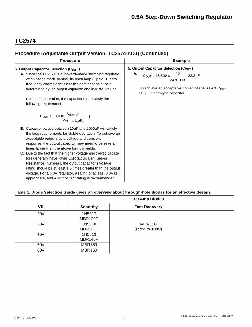
Table 1. Diode Selection Guide gives an overview about through-hole diodes for an effective design.
1.0 Amp Diodes
VR Schottky Fast Recovery
20V 1N5817MBR120P
30V 1N5818 MUR110MBR130P (rated to 100V)
40V 1N5819MBR140P
50V MBR15060V MBR160
11
TC2574
0.5A Step-Down Switching Regulator
TC2574-2 12/22/00© 2001 Microchip Technology Inc. DS21397A
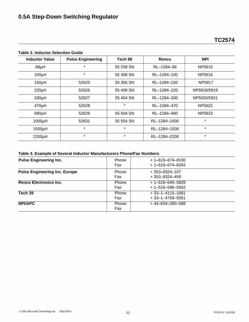
Table 2. Inductor Selection Guide
Inductor Value Pulse Engineering Tech 89 Renco NPI
68µH * 55 258 SN RL–1284–68 NP5915
100µH * 55 308 SN RL–1284–100 NP5916
150µH 52625 55 356 SN RL–1284–150 NP5917
220µH 52626 55 406 SN RL–1284–220 NP5918/5919
330µH 52627 55 454 SN RL–1284–330 NP5920/5921
470µH 52628 * RL–1284–470 NP5922
680µH 52629 55 504 SN RL–1284–680 NP5923
1000µH 52631 55 554 SN RL–1284–1000 *
1500µH * * RL–1284–1500 *
2200µH * * RL–1284–2200 *
Table 3. Example of Several Inductor Manufacturers Phone/Fax Numbers
Pulse Engineering Inc. Phone + 1–619–674–8100Fax + 1–619–674–8262
Pulse Engineering Inc. Europe Phone + 353–9324–107Fax + 353–9324–459
Renco Electronics Inc. Phone + 1–516–645–5828Fax + 1–516–586–5562
Tech 39 Phone + 33–1–4115–1681Fax + 33–1–4709–5051
NPI/APC Phone + 44–634–290–588Fax
TC2574
12TC2574-2 12/22/00
0.5A Step-Down Switching Regulator
© 2001 Microchip Technology Inc. DS21397A
EXTERNAL COMPONENTS
Input Capacitor (CIN)
The Input Capacitor Should Have a Low ESRFor stable operation of the switch mode converter a
lowESR (Equivalent Series Resistance) aluminium or solidtantalum bypass capacitor is needed between the inputpinand the ground pin, to prevent large voltage transientsfrom appearing at the input. It must be located near theregulator and use short leads. With most electrolytic capaci-tors, the capacitance value decreases and the ESR in-creases with lower temperatures. For reliable operation intemperatures below –25°C larger values of the input capaci-tor may be needed. Also paralleling a ceramic or solidtantalum capacitor will increase the regulator stability at coldtemperatures.
RMS Current Rating of CINThe important parameter of the input capacitor is the
RMS current rating. Capacitors that are physically large andhave large surface area will typically have higher RMScurrent ratings. For a given capacitor value, a higher voltageelectrolytic capacitor will be physically larger than a lowervoltage capacitor, and thus be able to dissipate more heat tothe surrounding air, and therefore will have a higher RMScurrent rating. The consequences of operating an electro-lytic capacitor beyond the RMS current rating is a shortenedoperating life. In order to assure maximum capacitor oper-ating lifetime, the capacitor’s RMS ripple current ratingshould be:
IRMS > 1.2 x d x ILOAD
where d is the duty cycle, for a continuous mode buckregualor
d = tON
= VOUT T VIN
and d = tON
= IVOUTI for a buck-boost regulator. T IVOUTI + VIN
Output Capacitor (COUT)For low output ripple voltage and good stability, low ESR
output capacitors are recommended. An output capacitorhas two main functions: it filters the output and providesregulator loop stability. The ESR of the output capacitor andthe peak–to–peak value of the inductor ripple current are themain factors contributing to the output ripple voltage value.Standard aluminium electrolytics could be adequate forsome applications but for quality design, low ESR types arerecommended.
An aluminium electrolytic capacitor’s ESR value is re-
lated to many factors, such as the capacitance value, thevoltage rating, the physical size and the type of construction.In most cases, the higher voltage electrolytic capacitorshave lower ESR value. Often capacitors with much highervoltage ratings may be needed to provide low ESR values,that are required for low output ripple voltage.
The Output Capacitor Requires an ESR Value that hasan Upper and Lower Limit
As mentioned above, a low ESR value is needed for lowoutput ripple voltage, typically 1% to 2% of the outputvoltage. But if the selected capacitor’s ESR is extremely low(below 0.03 Ω), there is a possibility of an unstable feedbackloop, resulting in oscillation at the output. This situation canoccur when a tantalum capacitor, that can have a very lowESR, is used as the only output capacitor.
At Low Temperatures, Put in Parallel AluminiumElectrolytic Capacitors with Tantalum Capacitors
Electrolytic capacitors are not recommended for tem-peratures below –25°C. The ESR rises dramatically at coldtemperatures and typically rises 3 times at –25°C and asmuch as 10 times at –40°C. Solid tantalum capacitors havemuch better ESR spec at cold temperatures and are recom-mended for temperatures below –25°C. They can be alsoused in parallel with aluminium electrolytics. The value of thetantalum capacitor should be about 10% or 20% of the totalcapacitance. The output capacitor should have at least50% higher RMS ripple current rating at 52kHz than thepeak–to–peak inductor ripple current.
Catch Diode
Locate the Catch Diode Close to the TC2574The TC2574 is a step–down buck converter, it requires
a fast diode to provide a return path for the inductor currentwhen the switch turns off. This diode must be located closeto the TC2574 using short leads and short printed circuittraces to avoid EMI problems.
Use a Schottky or a Soft SwitchingUltra–Fast Recovery Diode
Since the rectifier diodes are very significant source oflosses within switching power supplies, choosing the recti-fier that best fits into the converter design is an importantprocess. Schottky diodes provide the best performancebecause of their fast switching speed and low forwardvoltage drop.
They provide the best efficiency especially in low outputvoltage applications (5.0 V and lower). Another choice couldbe Fast–Recovery, or Ultra–Fast Recovery diodes. It has tobe noted, that some types of these diodes with an abruptturnoff characteristic may cause instability or EMI troubles.
13
TC2574
0.5A Step-Down Switching Regulator
TC2574-2 12/22/00© 2001 Microchip Technology Inc. DS21397A
A fast-recovery diode with soft recovery characteristicscan better fulfill some quality, low noise designrequirements.Table 1 provides a list of suitable diodes forthe TC2574 regulator. Standard 50/60Hz rectifier diodes,such as the 1N4001 series or 1N5400 series are NOTsuitable.
InductorThe magnetic components are the cornerstone of all
switching power supply designs. The style of the core andthe winding technique used in the magnetic component’sdesign have a great influence on the reliability of the overallpower supply.
Using an improper or poorly designed inductor cancause high voltage spikes generated by the rate of transi-tions in current within the switching power supply, and thepossibility of core saturation can arise during an abnormaloperational mode. Voltage spikes can cause the semicon-ductors to enter avalanche breakdown and the part caninstantly fail if enough energy is applied. It can also causesignificant RFI (Radio Frequency Interference) and EMI(Electro–Magnetic Interference) problems.
Continuous and Discontinuous Mode of Operation.The TC2574 step–down converter can operate in both
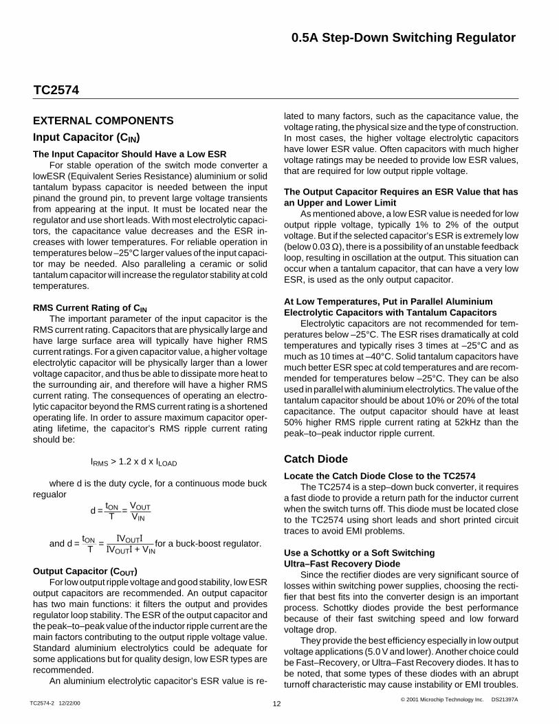
the continuous and the discontinuous modes of operation.The regulator works in the continuous mode when loads arerelatively heavy, the current flows through the inductorcontinuously and never falls to zero. Under light load condi-tions, the circuit will be forced to the discontinuousmodewhen inductor current falls to zero for certain period of time(see Figure 5 and Figure 6). Each mode has distinctivelydifferent operating characteristics, which can affect theregulator performance and requirements. In many cases thepreferred mode of operation is the continuous mode. It offers
greater output power, lower peak currents in the switch,inductor and diode, and can have a lower output ripplevoltage. On the other hand it does require larger inductorvalues to keep the inductor current flowing continuously,especially at low output load currents and/orhigh inputvoltages.
To simplify the inductor selection process, an inductorselection guide for the TC2574 regulator was added to thisdata sheet (Figures 39 through 41). This guide assumes thatthe regulator is operating in the continuous mode, andselects an inductor that will allow a peak–to–peak inductorripple current to be a certain percentage of the maximumdesign load current. This percentage is allowed to changeas different design load currents are selected. For light loads(less than approximately 0.2A) it may be desirable to oper-ate the regulator in the discontinuous mode, because theinductor value and size can be kept relatively low. Conse-quently, the percentage of inductor peak-to-peak currentincreases. This discontinuous mode of operation is perfectlyacceptable for this type of switching converter. Any buckregulator will be forced to enter discontinuous mode if theload current is light enough.
Selecting the Right Inductor Style
Some important considerations when selecting acoretype are core material, cost, the output power of thepowersupply, the physical volume the inductor must fitwithin, and the amount of EMI (Electro–Magnetic Interfer-ence) shielding that the core must provide. There are manydifferent styles of inductors available, such as pot core,E–core, toroid and bobbin core, as well as different corematerials such as ferrites and powdered iron from differentmanufacturers.
For high quality design regulators the toroid core seemsto be the best choice. Since the magnetic flux is contained
Figure 5. Continuous Mode Switching Current Waveforms
0.5AInductorCurrent
Waveform
PowerSwitch
CurrentWaveform
0A
0.5A
0A
HORIZONTAL TIME BASE: 5.0µsec/DIV
VE
RT
ICA
L R
ES
OL
UT
ION
200
mA
DV
Continuous Mode Switching CurrentWaveforms
Figure 6. Continuous Mode Switching Current Waveforms
0.1AInductorCurrent
Waveform
PowerSwitch
CurrentWaveform
0A
0.1A
0A
HORIZONTAL TIME BASE: 5.0µsec/DIV
VE
RT
ICA
L R
ES
OL
UT
ION
100
mA
DV
Continuous Mode Switching CurrentWaveforms
TC2574
14TC2574-2 12/22/00
0.5A Step-Down Switching Regulator
© 2001 Microchip Technology Inc. DS21397A
within the core, it generates less EMI, reducing noise prob-lems in sensitive circuits. The least expensive is the bobbincore type, which consists of wire wound on a ferrite rod core.This type of inductor generates more EMI due to the fact thatits core is open, and the magnetic flux is not contained withinthe core.
When multiple switching regulators are located on thesame printed circuit board, open core magnetics can causeinterference between two or more of the regulator circuits,especially at high currents due to mutual coupling. A toroid,pot core or E–core (closed magnetic structure) should beused in such applications.
Do Not Operate an Inductor Beyond itsMaximum Rated Current
Exceeding an inductor’s maximum current rating maycause the inductor to overheat because of the copper wirelosses, or the core may saturate. Core saturation occurswhen the flux density is too high and consequently the crosssectional area of the core can no longer support additionallines of magnetic flux.
This causes the permeability of the core to drop, theinductance value decreases rapidly and the inductor beginsto look mainly resistive. It has only the DC resistance of thewinding. This can cause the switch current to rise veryrapidly and force the TC2574 internal switch into cycle–by–cycle current limit, thus reducing the DC output load current.This can also result in overheating of the inductor and/or theTC2574. Different inductor types have different saturationcharacteristics, and this should be kept in mind when select-ing an inductor.
GENERAL RECOMMENDATIONS
Output Voltage Ripple and TransientsSource of the Output Ripple
Since the TC2574 is a switch mode power supplyregulator, its output voltage, if left unfiltered, will contain asawtooth ripple voltage at the switching frequency. Theoutput ripple voltage value ranges from 0.5% to 3% of theoutput voltage. It is caused mainly by the inductor sawtoothripple current multiplied by the ESR of the output capacitor.
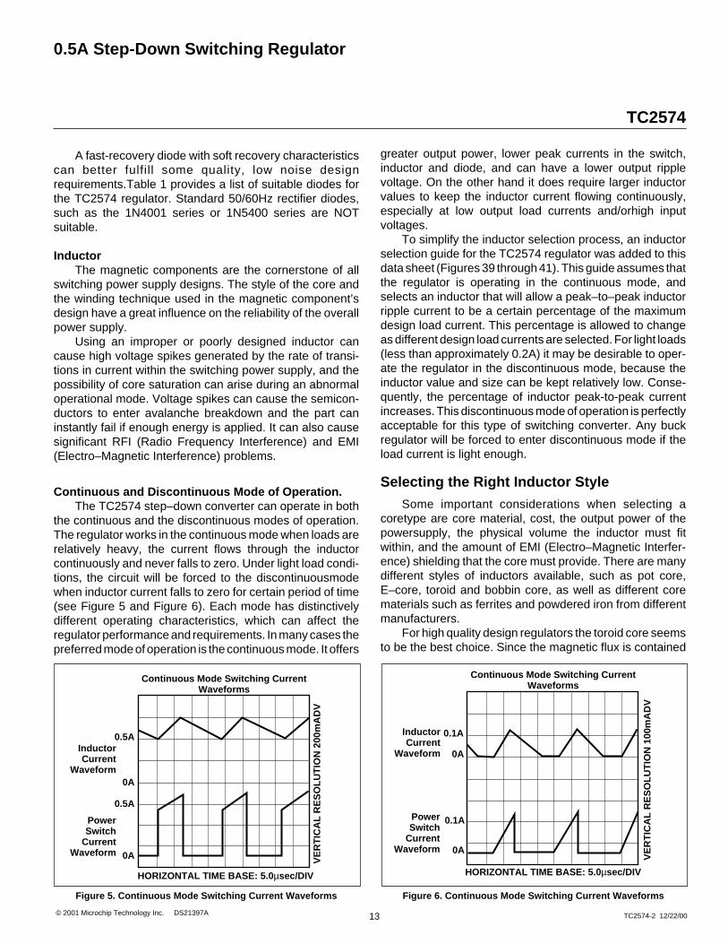
Short Voltage Spikes and How toReduce Them
The regulator output voltage may also contain shortvoltage spikes at the peaks of the sawtooth waveform (seeFigure 7). These voltage spikes are present because of thefast switching action of the output switch, and the parasiticinductance of the output filter capacitor. There are someother important factors such as wiring inductance, straycapacitance, as well as the scope probe used to evaluate
these transients, all these contribute to the amplitude ofthese spikes. To minimize these voltage spikes, low induc-tance capacitors should be used, and their lead lengthsmust be kept short. The importance of quality printed circuitboard layout design should also be highlighted.
Minimizing the Output Ripple
In order to minimize the output ripple voltage it ispossible to enlarge the inductance value of the inductor L1and/or to use a larger value output capacitor. There is alsoanother way to smooth the output by means of an additionalLC filter (20µH, 100µF), that can be added to the output (seeFigure 16) to further reduce the amount of output ripple andtransients. With such a filter it is possible to reduce theoutput ripple voltage transients 10 times or more. Figure 7shows the difference between filtered and unfiltered outputwaveforms of the regulator shown in Figure 15.
The upper waveform is from the normal unfilteredoutput of the converter, while the lower waveform shows theoutput ripple voltage filtered by an additional LC filter.
Heatsinking and Thermal Considerations
The TC2574 is available in both 8-Pin PDIP (narrow)and 16-Pin SOIC (wide) packages. When used in the typicalapplication the copper lead frame conducts the majority ofthe heat from the die, through the leads, to the printed circuitcopper. The copper and the board are the heatsink for thispackage and the other heat producing components, such asthe catch diode and inductor.
For the best thermal performance, wide copper tracesshould be used and all ground and unused pins should besoldered to generous amounts of printed circuit boardcopper, such as a ground plane. Large areas of copperprovide the best transfer of heat to the surrounding air. One
Figure 7. Output Ripple Voltage Waveforms
UnfilteredOutput
Voltage
FilteredOutput
Voltage
HORIZONTAL TIME BASE: 5.0µsec/DIV
VE
RT
ICA
L R
ES
OL
UT
ION
20m
V.D
IV
Voltage spikes caused by switching actionof the output switch and the parasitic inductanceof the output capacitor

15
TC2574
0.5A Step-Down Switching Regulator
TC2574-2 12/22/00© 2001 Microchip Technology Inc. DS21397A
exception to this is the output (switch) pin, which should nothave large areas of copper in order to minimize coupling tosensitive circuitry.
Additional improvement in heat dissipation can beachieved even by using of double sided or multilayer boardswhich can provide even better heat path to the ambient.
Using a socket for the 8-Pin PDIP (narrow) package isnot recommended because socket represents an additionalthermal resistance, and as a result the junction temperaturewill be higher.
Since the current rating of the TC2574 is only 0.5 A, thetotal package power dissipation for this switcher is quite low,ranging from approximately 0.1Ω up to 0.75Ω under varyingconditions. In a carefully engineered printed circuit board,the through–hole PDIP package can easily dissipate up to0.75 Ω, even at ambient temperatures of 60°C, and still keepthe maximum junction temperature below 125°C.
Thermal Analysis and Design
The following procedure must be performed to deter-mine the operating junction temperature. First determine:
1. PD(max) – maximum regulator power dissipation in theapplication.
2. TA(max) – maximum ambient temperature in theapplication.
3. TJ (max) – maximum allowed junction temperature(125°C for the TC2574). For a conservative design, themaximum junction temperature should not exceed 110°Cto assure safe operation. For every additional +10°C tem-perature rise that the junction must withstand, the estimatedoperating lifetime of the component is halved.
4. ΘJC – package thermal resistance junction–case.
5. ΘJA – package thermal resistance junction–ambient.
(Refer to Absolute Maximum Ratings on page 2 of thisdata sheet or ΘJC and ΘJA values).
The following formula is to calculate the approximatetotal power dissipated by the TC2574:
PD = (VIN x IQ ) + d x ILOAD x VSAT
where d is the duty cycle and for buck converter
d = tON = VO
T VIN
IQ (quiescent current) and VSAT can be found in theTC2574 data sheet,
VIN is minimum input voltage applied,VO is the regulator output voltage,ILOAD is the load current.
The dynamic switching losses during turn-on andturn-off can be neglected if a proper type catch diode is used.The junction temperature can be determined by the follow-ing expression:
TJ = (ΘJA )(PD ) + TA
where (ΘJA )(PD ) represents the junction temperature risecaused by the dissipated power and TA is the maximumambient temperature.
Some Aspects That can InfluenceThermal Design
It should be noted that the package thermal resistanceand the junction temperature rise numbers are all approxi-mate, and there are many factors that will affect thesenumbers, such as PC board size, shape, thickness, physicalposition, location, board temperature, as well as whether thesurrounding air is moving or still. At higher power levels thethermal resistance decreases due to the increased aircurrent activity.
Other factors are trace width, total printed circuit copperarea, copper thickness, single– or double–sided, multilayerboard, the amount of solder on the board or even color of thetraces.
The size, quantity and spacing of other components onthe board can also influence its effectiveness to dissipatethe heat. Some of them, like the catch diode or the inductorwill enerate some additional heat.
Figure 8. Inverting Buck-Boost Develops –12V
D1MBR150
L168 mH
Output
7
1
Feedback8.0 to 25 VUnregulated
DC Input
5
34 ON/OFFPwrGND
+VIN
–12 V @ 100mARegulated
Output
TC2574(12V)
2 SigGND
COUT680µF
CIN*22µF
TC2574
16TC2574-2 12/22/00
0.5A Step-Down Switching Regulator
© 2001 Microchip Technology Inc. DS21397A
ADDITIONAL APPLICATIONS
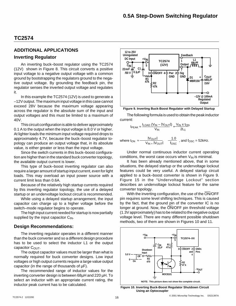
Inverting Regulator
An inverting buck–boost regulator using the TC2574(12V) shown in Figure 8. This circuit converts a positiveinput voltage to a negative output voltage with a commonground by bootstrapping the regulators ground to the nega-tive output voltage. By grounding the feedback pin, theregulator senses the inverted output voltage and regulatesit.
In this example the TC2574 (12V) is used to generate a–12V output. The maximum input voltage in this case cannotexceed 28V because the maximum voltage appearingacross the regulator is the absolute sum of the input andoutput voltages and this must be limited to a maximum of40V.
This circuit configuration is able to deliver approximately0.1 A to the output when the input voltage is 8.0 V or higher.At lighter loads the minimum input voltage required drops toapproximately 4.7V, because the buck–boost regulator to-pology can produce an output voltage that, in its absolutevalue, is either greater or less than the input voltage.
Since the switch currents in this buck–boost configura-tion are higher than in the standard buck converter topology,the available output current is lower.
This type of buck–boost inverting regulator can alsorequire a larger amount of startup input current, even for lightloads. This may overload an input power source with acurrent limit less than 0.6A.
Because of the relatively high startup currents requiredby this inverting regulator topology, the use of a delayedstartup or an undervoltage lockout circuit is recommended.
While using a delayed startup arrangement, the inputcapacitor can charge up to a higher voltage before theswitch–mode regulator begins to operate.
The high input current needed for startup is now partiallysupplied by the input capacitor CIN.
Design Recommendations:
The inverting regulator operates in a different mannerthan the buck converter and so a different design procedurehas to be used to select the inductor L1 or the outputcapacitor COUT.
The output capacitor values must be larger than what isnormally required for buck converter designs. Low inputvoltages or high output currents require a large value outputcapacitor (in the range of thousands of µF).
The recommended range of inductor values for theinverting converter design is between 68µH and 220 µH. Toselect an inductor with an appropriate current rating, theinductor peak current has to be calculated.
The following formula is used to obtain the peak inductorcurrent:
IPEAK ≈ ILOAD (VIN – IVOUTI)
+ VIN x tON
VIN 2L1
where tON ≈ IVOUTI 1.0 , and fOSC = 52kHz.
VIN + IVOUTI fOSC
Under normal continuous inductor current operatingconditions, the worst case occurs when VIN is minimal.
It has been already mentioned above, that in somesituations, the delayed startup or the undervoltage lockoutfeatures could be very useful. A delayed startup circuitapplied to a buck–boost converter is shown in Figure 9.Figure 15 in the “Undervoltage Lockout” sectiondescribes an undervoltage lockout feature for the sameconverter topology.
With the inverting configuration, the use of the ON/OFFpin requires some level shifting techniques. This is causedby the fact, that the ground pin of the converter IC is nolonger at ground. Now, the ON/OFF pin threshold voltage(1.3V approximately) has to be related to the negative outputvoltage level. There are many different possible shutdownmethods, two of them are shown in Figures 10 and 11.
Figure 9. Inverting Buck-Boost Regulator with Delayed Startup
D1MBR150
L168 µHOutput
7
1
Feedback12 to 25V
UnregulatedDC Input
CIN22 mF
/50 V
5
43 ON/OFF PwrGND
+VIN
–12V @ 100mARegulated
Output
COUT680 µF/16V
TC2574(12V)
C10.1 µF
R147k R2
47k
2 SigGND
Figure 10. Inverting Buck-Boost Regulator Shutdown Circuit Using an Optocoupler
TC2574–XX5
2and
4
3 GNDsPins
ON/OFF
+VIN
R247 k
CIN22µF
NOTE: This picture does not show the complete circuit.
R147 k
R3470
ShutdownInput
MOC8101
–VOUT
Off
On
5.0 V
0
+VIN

17
TC2574
0.5A Step-Down Switching Regulator
TC2574-2 12/22/00© 2001 Microchip Technology Inc. DS21397A
Negative Boost Regulator
This example is a variation of the buck–boost topologyand it is called negative boost regulator. This regulatorexperiences relatively high switch current, especially at lowinput voltages. The internal switch current limiting results inlower output load current capability.
The circuit in Figure 12 shows the negative boostconfiguration. The input voltage in this application rangesfrom –5.0 to –12V and provides a regulated –12V output. Ifthe input voltage is greater than –12V, the output will riseabove –12 V accordingly, but will not damage the regulator.
Design Recommendations:
The same design rules as for the previous invertingbuck–boost converter can be applied. The output capacitorCOUT must be chosen larger than what would be required fora standard buck converter. Low input voltages or high outputcurrents require a large value output capacitor (in the rangeof thousands of µF). The recommended range of inductorvalues for the negative boost regulator is the same as forinverting converter design.
Figure 12. Negative Boost Regulator
Figure 11. Inverting Buck-Boost Regulator Shutdown Circuit Using a PNP Transistor
Another important point is that these negative boostconverters cannot provide any current limiting load protec-tion in the event of a short in the output so some othermeans, such as a fuse, may be necessary to provide theload protection.
Delayed Startup
There are some applications, like the inverting regulatoralready mentioned above, which require a higher amount ofstart-up current. In such cases, if the input power source islimited, this delayed start-up feature becomes very useful.
To provide a time delay between the time when the inputvoltage is applied and the time when the output voltagecomes up, the circuit in Figure 13 can be used. As the inputvoltage is applied, the capacitor C1 charges up, and thevoltage across the resistor R2 falls down. When the voltageon the ON/OFF pin falls below the threshold value 1.3 V,the regulator starts up. Resistor R1 is included to limit themaximum voltage applied to the ON/OFF pin. It reduces thepower supply noise sensitivity, and also limits the capacitorC1 discharge current, but its use is not mandatory.
When a high 50Hz or 60Hz (100Hz or 120Hz respec-tively) ripple voltage exists, a long delay time can causesome problems by coupling the ripple into the ON/OFF pin,the regulator could be switched periodically on and off withthe line (or double) frequency.
Undervoltage Lockout
Some applications require the regulator to remain offuntil the input voltage reaches a certain threshold level.Figure 14 shows an undervoltage lockout circuit applied toa buck regulator. A version of this circuit for buck–boostconverter is shown in Figure 15. Resistor R3 pulls theON/OFF pin high and keeps the regulator off until the inputvoltage reaches an predetermined threshold level, which isdetermined by the following expression:
1N5817
330µH
Output
7
1
Feedback
VOUT = –12V
Load Current60mA for VIN = –5.2V120mA for VIN = –7.0V
VINL1
D1
COUT1000µF
CIN22µF
TC2574(12V)5
34 ON/OFFPwrGND
+VIN
2 SigGND
–5.0 to –12 V
NOTE: This picture does not show the complete circuit.
R25.6 k
Q12N3906
TC25745
2and
4
3 GNDsPins
ON/OFF
R112 k –VOUT
+VIN
ShutdownInputOff
On
+V
0
+VIN
Cin22µF
Figure 13. Delayed Startup Circuitry
R147 k
TC25745
2and
4
3 GNDsand Pins
ON/OFF
R247 k
+VIN +VIN
C10.1 µF
CIN22mF
NOTE: This picture does not show the complete circuit.

TC2574
18TC2574-2 12/22/00
0.5A Step-Down Switching Regulator
© 2001 Microchip Technology Inc. DS21397A
VTH ≈
VZ1 +(1.0 +
R2 ) VBE (Q1)
R1
Figure 14. Undervoltage Lockout Circuit for Buck Converter
R110k
Z11N5242B
R210k
Q12N3904
R347k
CIN22µF
TC2574(5V)5
2and
4
3 GNDsPins
ON/OFF
+VIN +VIN
NOTE: This picture does not show the complete circuit.
Figure 15. Undervoltage Lockout Circuit for Buck-Boost Converter
R215 k
Z11N5242
R115 k
Q12N3904
R368 k
Cin22mF
TC2574(5V)5
2and
4
3 GNDsPins
ON/OFF
+VIN +VIN
–VOUT
NOTE: This picture does not show the complete circuit (see Figure 8).
Adjustable Output, Low-Ripple Power Supply
A 0.5 A output current capability power supply thatfeatures an adjustable output voltage is shown in Figure 16.This regulator delivers 0.5 A into 1.2 to 35 V output. The inputvoltage ranges from roughly 3.0 to 40 V. In order to achievea 10 or more times reduction of output ripple, an additionalL–C filter is included in this circuit.
Figure 16. 1.2 to 35V Adjustable 500mA Power Supply with Low Output Ripple
D11N5819
L1150µH
Output
7
1
Feedback
R250 k
R11.1 k
L220µH
OutputVoltage
1.2 to 35V @ 0.5 A
Optional OutputRipple Filter
40V MaxUnregulatedDC Input
COUT1000µF
C1100µF
CIN22µF
TC2574–ADJ5
34 PwrGND
+VIN
2 SigGND
ON/OFF

19
TC2574
0.5A Step-Down Switching Regulator
TC2574-2 12/22/00© 2001 Microchip Technology Inc. DS21397A
Figure 17. Schematic Diagram of the TC2574 (5V) Step-Down Converter
The TC2574–5 Step-Down Voltage Regulator with 5.0V @ 0.5A Output Power Capability.Typical Application with Through-Hole PC Board Layout
D11N5819
L1330µH
Output
7
1
Feedback
UnregulatedDC Input
+VIN = 7.0 to 40 V
C2220µF
C1220µF
TC2574(5V)5
4 3PwrGND
+VIN
Regulated Output+VOUT = 5.0V @ 0.5 A
GND
C1 – 22µF, 63V, Aluminum ElectrolyticC2 – 220µF, 16V, Aluminum ElectrolyticD1 – 1.0A, 40V, Schotty Rectifier, 1N5819L1 – 330µH, RL-1284-330, Renco Electronics
GND
2 SigGND
ON/OFF
Figure 18. PC Board Layout Component Side Figure 19. PC Board Layout Copper Side
TC2574–5.0
C1 C2+
+U1
L1
D1VOUT
GND
GND
+VIN
NOTE: Not to scale. NOTE: Not to scale.

TC2574
20TC2574-2 12/22/00
0.5A Step-Down Switching Regulator
© 2001 Microchip Technology Inc. DS21397A
Figure 20. Schematic Diagram of the 5.0V @ 0.5A Step-Down Converter Using the TC2574–ADJ(An additional LC filter is included to achieve low output ripple voltage)
D11N5819
L1330µH
Output
7
1
Feedback
R26.12 kW
R12.0 kW
L222µH
RegulatedOutput Filtered
VOUT = 5.0 V @ 0.5 A
OutputRipple Filter
UnregulatedDC Input
C2220µF
C3100µF C1
22µF
TC2574–ADJ5
3 ON/OFFPwrGND
+VIN
24 SigGND
+Vin = 7.0 to 40 V
GND GND
The TC2574–ADJ Step-Down Voltage Regulator with 5.0V @ 0.5A Output Power Capability.Typical Application with Through-Hole PC Board Layout
C1 – 22µF, 63V, Aluminum ElectrolyticC2 – 220µF, 16V, Aluminum ElectrolyticC3 – 100µF, 16V Aluminum ElectrolyticD1 – 1.0A, 40V, Schotty Rectifier, 1N5829L1 – 330µH, RL–1284–330, Renco ElectronicsL2 – 25µH, SFT52501, TDKR1 – 2.0kΩ, 0.1%, 0.25WR2 – 6.12kΩ, 0.1%, 0.25W
Figure 21. PC Board Layout Component Side Figure 22. PC Board Layout Copper Side
TC2574
C1 C2+
+U1
L1
D1
VOUTGND
+VIN C3+ GND
L2
R1 R2
NOTE: Not to scale. NOTE: Not to scale.

21
TC2574
0.5A Step-Down Switching Regulator
TC2574-2 12/22/00© 2001 Microchip Technology Inc. DS21397A
TYPICAL CHARACTERISTICS (Circuit of Figure 2)
VIN, INPUT VOLTAGE (V)
Figure 23. Normalized Output Voltage Figure 24. Line Regulation
VIN = 20VILOAD = 100mANormalized at TJ = 25°C
Figure 25. Dropout Voltage Figure 26. Current Limit
Figure 27. Quiescent Current Figure 28. Standby Quiescent Current
ILOAD = 100mATJ = 25°C
3.3V , 5.0V and ADJ
12V
VIN = 25 V
ILOAD = 100mA
ILOAD = 500mA
VIN = 12 V
VIN = 40 V
L = 300µH
ILOAD = 500mA
ILoad = 100mA
VOUT = 5.0 VMeasured atGround PinTJ = 25°C
VON/OFF = 5.0 V
1.0
0.8
0.6
0.4
0.2
0
–0.2
–0.4
–0.6
–0.8
–1.0
1.4
1.2
1.0
0.8
0.6
0.4
0.2
0
–0.2
–0.4
–0.6
2.0
1.5
1.0
0.5
0
1.4
1.3
1.2
1.1
1.0
0.9
0.8
0.7
20
18
16
14
12
10
8.0
6.0
4.0
200
180
160
140
120
100
80
60
40
200
1251007560250–25–50 403530252015105.00
1251007560250–5–50 1251007560250–25–50
403530252015105.00 1251007560250–25–50
VO
UT
,OU
TP
UT
VO
LT
AG
E C
HA
NG
E (
%)
INP
UT
- O
UT
PU
T D
IFF
ER
EN
TIA
L (
V)
I O, O
UT
PU
T C
UR
RE
NT
(A
)I S
TB
Y, S
TA
ND
AB
Y C
UR
RE
NT
(A
)
I Q, Q
UIE
SC
EN
T C
UR
RE
NT
(m
A)
VO
UT
,OU
TP
UT
VO
LT
AG
E C
HA
NG
E (
%)
TJ JUNCTION TEMPERATURE (°C)
TJ JUNCTION TEMPERATURE (°C)
VIN INPUT VOLTAGE (V)
TJ JUNCTION TEMPERATURE (°C)
TJ JUNCTION TEMPERATURE (°C)

TC2574
22TC2574-2 12/22/00
0.5A Step-Down Switching Regulator
© 2001 Microchip Technology Inc. DS21397A
TYPICAL CHARACTERISTICS (Circuit of Figure 2 Cont.)
I FB, F
EEDB
ACK
PIN
CURR
ENT (
nA)
A
B
C
TJ, JUNCTION TEMPERATURE (5C)
5 µsec/DIV5 µsec/DIV
NORM
ALIZ
ED F
REQ
UENC
Y (%
)
Figure 29. Oscillator Frequency Figure 30. Switch Saturation Voltage
Figure 31. Minimum Operating V Figure 32. Feedback Pin Currentoltage
Figure 33. Continuous Mode Switching Waveforms VOUT = 5.0V, 500mA Load Current, L = 330µH VOUT = 5.0V, 100mA Load Current, L = 100µH
Figure 34. Discontinuous Mode Switching Waveforms
VIN = 1.23VILOAD = 100mA
VIN = 12 VNormalized at 25°C
Adjustable Version OnlyAdjustable Version Only
A
B
C
A: Output Pin Voltage 10V/DIV.B: Inductor Current, 0.2 A/DIV..C: Output Ripple Voltage, 20mV/DIV, AC-Coupled
A: Output Pin Voltage 10V/DIV.B: Inductor Current, 0.2 A/DIV..C: Output Ripple Voltage, 20mV/DIV, AC-Coupled
8.0
6.0
4.0
2.0
0
–2.0
–4.0
–6.0
–8.0
10
1.3
1.2
1.1
1.0
0.9
0.8
0.7
0.6
0.5
0.40.3
5.0
4.5
4.0
3.5
3.0
2.5
2.0
1.5
1.0
0.5
0
100
80
60
40
20
0
–20
–0
–60
–80
–100
1251007550250–25–50 0 0.1 0.2 0.3 0.4 0.5
1251007550250±25±50 1251007550250–25–50
20V
10V
0
0.6A
0.4A
0.2A
0
20mVAC
20V
10V
0
0.6A
0.4A
0.2A
0
20mVAC
–40°C
25°C
125°C
TJ JUNCTION TEMPERATURE (°C)
TJ JUNCTION TEMPERATURE (°C)
SWITCH CURRENT (A)V
SA
T, S
AT
UR
AT
ION
VO
LT
AG
E (
V)
VIN
, IN
PU
T V
OL
TA
GE
(V
)
23
TC2574
0.5A Step-Down Switching Regulator
TC2574-2 12/22/00© 2001 Microchip Technology Inc. DS21397A
TYPICAL CHARACTERISTICS (Circuit of Figure 2 Cont.)
A
B
Figure 35. 500mA Load Transient Response forContinuous Mode Operation, L = 330 µH, COUT = 300µF
Figure 36. 250mA Load Transient Response forDisontinuous Mode Operation, L = 68µH, COUT = 470µF
A
B
50mVAC
500mA
200µsec/DIV 200µsec/DIV
0
50 mVAC
200 mA
100 mA
0
A: Output Pin Voltage 50V/DIV, AC CoupledB: 100mA to 500mA Load Pulse
A: Output Pin Voltage 50V/DIV, AC CoupledB: 50mA to 250mA Load Pulse.
V IN, M
AXIM
UM IN
PUT
VOLT
AGE
(V)
V IN, M
AXIM
UM IN
PUT
VOLT
AGE
(V)
V IN, M
AXIM
UM IN
PUT
VOLT
AGE
(V)
IL, MAXIMUM LOAD CURRENT (A)
IL, MAXIMUM LOAD CURRENT (A)IL, MAXIMUM LOAD CURRENT (A)
Figure 37. TC2574 (VOUT = 3.3V)
IL, MAXIMUM LOAD CURRENT (A)
Figure 38. TC2574 (VOUT = 5.0V)
680
Figure 39. TC2574 (VOUT = 12.0V) Figure 40. TC2574–ADJ
150
470
220
100
330
1000
330
680
470
150
220
2200
470
1500
1000
330
680
220
2200
470
15001000
330
680
220150
100
68
60201512109.08.07.0
6.0
5.0
60
30
2015
12
10
9.0
8.0
7.0
60
403025
20
1817
16
15
14
250200150
10080
60504030
2015
10
0.50.40.30.20.150.1 0.50.40.30.20.150.1
0.50.40.30.20.150.1 0.50.40.30.20.150.1
ET
, VO
LT
AG
E T
IME
(µs
ec)
TYPICAL CHARACTERISTICS (Circuit of Figure 16 Cont.)
TC2574
24TC2574-2 12/22/00
0.5A Step-Down Switching Regulator
© 2001 Microchip Technology Inc. DS21397A
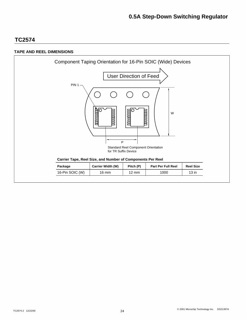
TAPE AND REEL DIMENSIONS
PIN 1
Component Taping Orientation for 16-Pin SOIC (Wide) Devices
User Direction of Feed
Standard Reel Component Orientationfor TR Suffix Device
W
P
Package Carrier Width (W) Pitch (P) Part Per Full Reel Reel Size
16-Pin SOIC (W) 16 mm 12 mm 1000 13 in
Carrier Tape, Reel Size, and Number of Components Per Reel

25
TC2574
0.5A Step-Down Switching Regulator
TC2574-2 12/22/00© 2001 Microchip Technology Inc. DS21397A
PACKAGE DIMENSIONS
Dimensions: inches (mm)
8-Pin PDIP (Narrow)
3° MIN.
PIN 1
.260 (6.60)
.240 (6.10)
.045 (1.14)
.030 (0.76).070 (1.78).040 (1.02)
.400 (10.16).348 (8.84)
.200 (5.08)
.140 (3.56)
.150 (3.81)
.115 (2.92)
.110 (2.79)
.090 (2.29).022 (0.56).015 (0.38)
.040 (1.02)
.020 (0.51) .015 (0.38).008 (0.20)
.310 (7.87)
.290 (7.37)
.400 (10.16).310 (7.87)

TC2574
26TC2574-2 12/22/00
0.5A Step-Down Switching Regulator
© 2001 Microchip Technology Inc. DS21397A
Information contained in this publication regarding device applications and the like is intended through suggestion only and may be superseded byupdates. It is your responsibility to ensure that your application meets with your specifications. No representation or warranty is given and no liability isassumed by Microchip Technology Incorporated with respect to the accuracy or use of such information, or infringement of patents or other intellectualproperty rights arising from such use or otherwise. Use of Microchipís products as critical components in life support systems is not authorized except withexpress written approval by Microchip. No licenses are conveyed, implicitly or otherwise, except as maybe explicitly expressed herein, under any intellec-tual property rights. The Microchip logo and name are registered trademarks of Microchip Technology Inc. in the U.S.A. and other countries. All rightsreserved. All other trademarks mentioned herein are the property of their respective companies.
All rights reserved. © 2001 Microchip Technology Incorporated. Printed in the USA. 1/01 Printed on recycled paper.
AMERICASCorporate Office2355 West Chandler Blvd.Chandler, AZ 85224-6199Tel: 480-792-7200 Fax: 480-792-7277Technical Support: 480-792-7627Web Address: http://www.microchip.comRocky Mountain2355 West Chandler Blvd.Chandler, AZ 85224-6199Tel: 480-792-7966 Fax: 480-792-7456
Atlanta500 Sugar Mill Road, Suite 200BAtlanta, GA 30350Tel: 770-640-0034 Fax: 770-640-0307AustinAnalog Product Sales8303 MoPac Expressway NorthSuite A-201Austin, TX 78759Tel: 512-345-2030 Fax: 512-345-6085Boston2 Lan Drive, Suite 120Westford, MA 01886Tel: 978-692-3848 Fax: 978-692-3821BostonAnalog Product SalesUnit A-8-1 Millbrook Tarry Condominium97 Lowell RoadConcord, MA 01742Tel: 978-371-6400 Fax: 978-371-0050Chicago333 Pierce Road, Suite 180Itasca, IL 60143Tel: 630-285-0071 Fax: 630-285-0075Dallas4570 Westgrove Drive, Suite 160Addison, TX 75001Tel: 972-818-7423 Fax: 972-818-2924DaytonTwo Prestige Place, Suite 130Miamisburg, OH 45342Tel: 937-291-1654 Fax: 937-291-9175DetroitTri-Atria Office Building 32255 Northwestern Highway, Suite 190Farmington Hills, MI 48334Tel: 248-538-2250 Fax: 248-538-2260Los Angeles18201 Von Karman, Suite 1090Irvine, CA 92612Tel: 949-263-1888 Fax: 949-263-1338Mountain ViewAnalog Product Sales1300 Terra Bella AvenueMountain View, CA 94043-1836Tel: 650-968-9241 Fax: 650-967-1590
New York150 Motor Parkway, Suite 202Hauppauge, NY 11788Tel: 631-273-5305 Fax: 631-273-5335San JoseMicrochip Technology Inc.2107 North First Street, Suite 590San Jose, CA 95131Tel: 408-436-7950 Fax: 408-436-7955Toronto6285 Northam Drive, Suite 108Mississauga, Ontario L4V 1X5, CanadaTel: 905-673-0699 Fax: 905-673-6509
ASIA/PACIFICChina - BeijingMicrochip Technology Beijing OfficeUnit 915New China Hong Kong Manhattan Bldg.No. 6 Chaoyangmen Beidajie Beijing, 100027, No. ChinaTel: 86-10-85282100 Fax: 86-10-85282104China - ShanghaiMicrochip Technology Shanghai OfficeRoom 701, Bldg. BFar East International PlazaNo. 317 Xian Xia RoadShanghai, 200051Tel: 86-21-6275-5700 Fax: 86-21-6275-5060Hong KongMicrochip Asia PacificRM 2101, Tower 2, Metroplaza223 Hing Fong RoadKwai Fong, N.T., Hong KongTel: 852-2401-1200 Fax: 852-2401-3431IndiaMicrochip Technology Inc.India Liaison OfficeDivyasree Chambers1 Floor, Wing A (A3/A4)No. 11, OíShaugnessey RoadBangalore, 560 025, IndiaTel: 91-80-2290061 Fax: 91-80-2290062JapanMicrochip Technology Intl. Inc.Benex S-1 6F3-18-20, ShinyokohamaKohoku-Ku, Yokohama-shiKanagawa, 222-0033, JapanTel: 81-45-471- 6166 Fax: 81-45-471-6122KoreaMicrochip Technology Korea168-1, Youngbo Bldg. 3 FloorSamsung-Dong, Kangnam-KuSeoul, KoreaTel: 82-2-554-7200 Fax: 82-2-558-5934
ASIA/PACIFIC (continued)SingaporeMicrochip Technology Singapore Pte Ltd.200 Middle Road#07-02 Prime CentreSingapore, 188980Tel: 65-334-8870 Fax: 65-334-8850TaiwanMicrochip Technology Taiwan11F-3, No. 207Tung Hua North RoadTaipei, 105, TaiwanTel: 886-2-2717-7175 Fax: 886-2-2545-0139
EUROPEAustraliaMicrochip Technology Australia Pty LtdSuite 22, 41 Rawson StreetEpping 2121, NSWAustraliaTel: 61-2-9868-6733 Fax: 61-2-9868-6755DenmarkMicrochip Technology Denmark ApSRegus Business CentreLautrup hoj 1-3Ballerup DK-2750 DenmarkTel: 45 4420 9895 Fax: 45 4420 9910FranceArizona Microchip Technology SARLParc díActivite du Moulin de Massy43 Rue du Saule TrapuBatiment A - ler Etage91300 Massy, FranceTel: 33-1-69-53-63-20 Fax: 33-1-69-30-90-79GermanyArizona Microchip Technology GmbHGustav-Heinemann Ring 125D-81739 Munich, GermanyTel: 49-89-627-144 0 Fax: 49-89-627-144-44GermanyAnalog Product SalesLochhamer Strasse 13D-82152 Martinsried, GermanyTel: 49-89-895650-0 Fax: 49-89-895650-22ItalyArizona Microchip Technology SRLCentro Direzionale Colleoni Palazzo Taurus 1 V. Le Colleoni 120041 Agrate BrianzaMilan, Italy Tel: 39-039-65791-1 Fax: 39-039-6899883United KingdomArizona Microchip Technology Ltd.505 Eskdale RoadWinnersh TriangleWokingham Berkshire, England RG41 5TUTel: 44 118 921 5869 Fax: 44-118 921-5820
01/09/01
WORLDWIDE SALES AND SERVICE