standard cell and full custom power-balanced logic: asic...
TRANSCRIPT

Newcastle University
School of Electrical, Electronic and Computer Engineering
Standard Cell and Full Custom Power-balanced Logic:
ASIC Implementation
Julian Murphy
Technical Report Series
NCL-EECE-2008-129
March 2008

Contact:
Supported by EPSRC grant GR/S81421.
NCL-EECE-2008-129
Copyright © 2008 Newcastle University
School of Electrical, Electronic and Computer Engineering
Newcastle University
Merz Court
Tyne and Wear
NE1 7RU, UK
http://async.org.uk

Contents
List of Figures ix
List of Tables xiii
Abstract xiv
1 Introduction 1
1.1 Research Goals and Contributions . . . . . . . . . . . . . . . . . . .. . 8
1.2 Thesis Structure . . . . . . . . . . . . . . . . . . . . . . . . . . . . . . . 11
2 A Primer in Cryptography and AES-128 13
2.1 Introduction . . . . . . . . . . . . . . . . . . . . . . . . . . . . . . . . . 14
2.1.1 Cryptographic Algorithms . . . . . . . . . . . . . . . . . . . . . 15
2.1.1.1 Asymmetric Encryption . . . . . . . . . . . . . . . . . 16
iii

CONTENTS
2.1.1.2 Symmetric Encryption . . . . . . . . . . . . . . . . . . 17
2.2 Number Theory . . . . . . . . . . . . . . . . . . . . . . . . . . . . . . . 18
2.2.1 Groups, Rings and Fields . . . . . . . . . . . . . . . . . . . . . . 18
2.2.2 Finite Field Polynomials . . . . . . . . . . . . . . . . . . . . . . 21
2.2.3 Construction of Finite Fields . . . . . . . . . . . . . . . . . . . .22
2.2.4 Bases of Finite Fields . . . . . . . . . . . . . . . . . . . . . . . . 22
2.3 Advanced Encryption Standard . . . . . . . . . . . . . . . . . . . . . .. 23
2.3.1 History . . . . . . . . . . . . . . . . . . . . . . . . . . . . . . . 23
2.3.2 AES-128 Algorithm . . . . . . . . . . . . . . . . . . . . . . . . 24
2.3.3 AES-128 Operations . . . . . . . . . . . . . . . . . . . . . . . . 27
2.3.3.1 SubBytes . . . . . . . . . . . . . . . . . . . . . . . . . 28
2.3.3.2 ShiftRow . . . . . . . . . . . . . . . . . . . . . . . . . 29
2.3.3.3 MixColumns . . . . . . . . . . . . . . . . . . . . . . . 30
2.3.3.4 AddRoundKey . . . . . . . . . . . . . . . . . . . . . . 30
2.3.3.5 Key Schedule . . . . . . . . . . . . . . . . . . . . . . 31
2.4 Cryptanalysis Attacks . . . . . . . . . . . . . . . . . . . . . . . . . . . .32
iv

CONTENTS
2.4.1 Linear Cryptanalysis . . . . . . . . . . . . . . . . . . . . . . . . 33
2.4.2 Differential Cryptanalysis . . . . . . . . . . . . . . . . . . . . .33
2.4.3 Side-channel Cryptanalysis . . . . . . . . . . . . . . . . . . . . 34
2.5 Summary . . . . . . . . . . . . . . . . . . . . . . . . . . . . . . . . . . 35
3 Power Analysis 37
3.1 Introduction . . . . . . . . . . . . . . . . . . . . . . . . . . . . . . . . . 37
3.1.1 Power . . . . . . . . . . . . . . . . . . . . . . . . . . . . . . . 42
3.1.1.1 Dynamic Dissipation . . . . . . . . . . . . . . . . . . 44
3.1.2 Switching Activity . . . . . . . . . . . . . . . . . . . . . . . . . 47
3.1.3 Timing . . . . . . . . . . . . . . . . . . . . . . . . . . . . . . . 49
3.1.4 Instantaneous Power . . . . . . . . . . . . . . . . . . . . . . . . 51
3.2 Simple Power Analysis . . . . . . . . . . . . . . . . . . . . . . . . . . . 52
3.3 Differential Power Analysis . . . . . . . . . . . . . . . . . . . . . . .. . 54
3.3.1 Power Bias Spikes . . . . . . . . . . . . . . . . . . . . . . . . . 60
3.3.2 Higher-order DPA attacks . . . . . . . . . . . . . . . . . . . . . 62
3.3.3 Variations of DPA . . . . . . . . . . . . . . . . . . . . . . . . . 63
v
CONTENTS
3.3.4 Conducting DPA . . . . . . . . . . . . . . . . . . . . . . . . . . 64
3.4 Power-balancing . . . . . . . . . . . . . . . . . . . . . . . . . . . . . . 65
3.4.1 Power-balancing Countermeasures . . . . . . . . . . . . . . . .. 69
3.5 Other Countermeasures . . . . . . . . . . . . . . . . . . . . . . . . . . . 75
3.5.1 Software Countermeasures . . . . . . . . . . . . . . . . . . . . . 75
3.5.1.1 Sophisticated Coding . . . . . . . . . . . . . . . . . . 75
3.5.1.2 Variable Splitting . . . . . . . . . . . . . . . . . . . . 77
3.5.1.3 Masking . . . . . . . . . . . . . . . . . . . . . . . . . 78
3.5.2 Hardware Countermeasures . . . . . . . . . . . . . . . . . . . . 78
3.5.2.1 Power Randomisation . . . . . . . . . . . . . . . . . . 78
3.5.2.2 Random Process Interrupts . . . . . . . . . . . . . . . 79
3.5.2.3 Detached Power Supplies . . . . . . . . . . . . . . . . 79
3.6 Summary . . . . . . . . . . . . . . . . . . . . . . . . . . . . . . . . . . 80
4 Power-balanced Standard Cell Logic: AES-128 ASIC 81
4.1 Introduction . . . . . . . . . . . . . . . . . . . . . . . . . . . . . . . . . 81
4.2 Power-balanced Standard Cell Logic . . . . . . . . . . . . . . . . .. . . 84
vi

CONTENTS
4.2.1 Alternating Spacer Logic . . . . . . . . . . . . . . . . . . . . . . 84
4.2.2 Direct Mapping Conversion . . . . . . . . . . . . . . . . . . . . 88
4.3 AES-128 Hardware Implementations . . . . . . . . . . . . . . . . . .. . 89
4.3.1 Datapath Width . . . . . . . . . . . . . . . . . . . . . . . . . . . 91
4.3.2 Encryption and Decryption . . . . . . . . . . . . . . . . . . . . . 91
4.3.3 Architectural Optimisations . . . . . . . . . . . . . . . . . . . .94
4.3.3.1 Pipelining and Loop Unrolling . . . . . . . . . . . . . 94
4.3.4 Algorithmic Optimisation . . . . . . . . . . . . . . . . . . . . . 95
4.3.4.1 SubBytes . . . . . . . . . . . . . . . . . . . . . . . . . 95
4.3.4.2 Key Schedule . . . . . . . . . . . . . . . . . . . . . . 97
4.4 AES-128 Architecture . . . . . . . . . . . . . . . . . . . . . . . . . . . 99
4.4.1 Interface . . . . . . . . . . . . . . . . . . . . . . . . . . . . . . 102
4.4.2 Control Unit . . . . . . . . . . . . . . . . . . . . . . . . . . . . 103
4.4.3 Data Unit . . . . . . . . . . . . . . . . . . . . . . . . . . . . . . 103
4.4.4 Key Unit . . . . . . . . . . . . . . . . . . . . . . . . . . . . . . 105
4.5 Case Study: AES-128 ASIC . . . . . . . . . . . . . . . . . . . . . . . . 106
4.5.1 Power Analysis Investigation . . . . . . . . . . . . . . . . . . . .109
4.6 Summary . . . . . . . . . . . . . . . . . . . . . . . . . . . . . . . . . . 116
vii
CONTENTS
5 Power-balanced Custom Cell Logic: AES-128 S-box ASIC 117
5.1 Introduction . . . . . . . . . . . . . . . . . . . . . . . . . . . . . . . . . 117
5.2 Power-balanced Custom Logic . . . . . . . . . . . . . . . . . . . . . . .119
5.2.1 Gate construction . . . . . . . . . . . . . . . . . . . . . . . . . . 119
5.2.2 Precharging . . . . . . . . . . . . . . . . . . . . . . . . . . . . 122
5.2.3 Cell Layout . . . . . . . . . . . . . . . . . . . . . . . . . . . . . 126
5.2.4 Design Construction . . . . . . . . . . . . . . . . . . . . . . . . 131
5.3 Case Study: AES-128 S-box ASIC . . . . . . . . . . . . . . . . . . . . . 134
5.3.1 Power Analysis Investigation . . . . . . . . . . . . . . . . . . . .135
5.4 Summary . . . . . . . . . . . . . . . . . . . . . . . . . . . . . . . . . . 142
6 Conclusions 143
Bibliography 146
viii

List of Figures
1.1 Smartcard power analysis . . . . . . . . . . . . . . . . . . . . . . . . . .6
1.2 Security pyramid . . . . . . . . . . . . . . . . . . . . . . . . . . . . . . 6
2.1 AES-128 algorithm . . . . . . . . . . . . . . . . . . . . . . . . . . . . . 26
2.2 State andCipherKey matrix . . . . . . . . . . . . . . . . . . . . . . . 28
2.3 SubBytes . . . . . . . . . . . . . . . . . . . . . . . . . . . . . . . . . . 29
2.4 ShiftRows . . . . . . . . . . . . . . . . . . . . . . . . . . . . . . . . . 30
2.5 MixColumns . . . . . . . . . . . . . . . . . . . . . . . . . . . . . . . . . 30
2.6 AddRoundKey . . . . . . . . . . . . . . . . . . . . . . . . . . . . . . . . 31
3.1 Inverter . . . . . . . . . . . . . . . . . . . . . . . . . . . . . . . . . . . 45
3.2 NAND gate . . . . . . . . . . . . . . . . . . . . . . . . . . . . . . . . . 48
3.3 SPA on DES rounds . . . . . . . . . . . . . . . . . . . . . . . . . . . . . 55
ix

LIST OF FIGURES
3.4 DPA flowchart . . . . . . . . . . . . . . . . . . . . . . . . . . . . . . . . 59
3.5 Two inverters switching through code-words to fixed state . . . . . . . . . 67
3.6 DIMS_1 NAND and differential trace . . . . . . . . . . . . . . . . . .. 71
3.7 DIMS_2 NAND and differential trace . . . . . . . . . . . . . . . . . .. 72
3.8 DIMS_3 NAND and differential trace . . . . . . . . . . . . . . . . . .. 72
3.9 DIMS_4 NAND and differential trace . . . . . . . . . . . . . . . . . .. 73
3.10 SABL NAND and differential trace . . . . . . . . . . . . . . . . . . .. 74
4.1 AES-128 ASIC . . . . . . . . . . . . . . . . . . . . . . . . . . . . . . . 82
4.2 Alternating spacers . . . . . . . . . . . . . . . . . . . . . . . . . . . . . 85
4.3 Alternating spacer switching cycle . . . . . . . . . . . . . . . . .. . . . 86
4.4 Alternating spacer logic and negative logic optimisation . . . . . . . . . . 86
4.5 Construction of dual-rail circuits . . . . . . . . . . . . . . . . .. . . . . 87
4.6 Datapath width . . . . . . . . . . . . . . . . . . . . . . . . . . . . . . . 92
4.7 Pipelining and loop unrolling . . . . . . . . . . . . . . . . . . . . . .. . 96
4.8 S-box architectures . . . . . . . . . . . . . . . . . . . . . . . . . . . . . 98
4.9 AES-128 core architecture . . . . . . . . . . . . . . . . . . . . . . . . .102
x

LIST OF FIGURES
4.10 Interface timing . . . . . . . . . . . . . . . . . . . . . . . . . . . . . . . 103
4.11 Data-unit . . . . . . . . . . . . . . . . . . . . . . . . . . . . . . . . . . 106
4.12 Key Unit . . . . . . . . . . . . . . . . . . . . . . . . . . . . . . . . . . . 107
4.13 AES-128 ASIC . . . . . . . . . . . . . . . . . . . . . . . . . . . . . . . 108
4.14 Verilog hierarchy . . . . . . . . . . . . . . . . . . . . . . . . . . . . . . 109
4.15 Original AES-128 core . . . . . . . . . . . . . . . . . . . . . . . . . . . 112
4.16 Dual-rail AES-128 core . . . . . . . . . . . . . . . . . . . . . . . . . . .113
4.17 Key hypotheses differential traces . . . . . . . . . . . . . . . .. . . . . 115
5.1 XOR gate . . . . . . . . . . . . . . . . . . . . . . . . . . . . . . . . . . 121
5.2 OR gate . . . . . . . . . . . . . . . . . . . . . . . . . . . . . . . . . . . 123
5.3 AND gate . . . . . . . . . . . . . . . . . . . . . . . . . . . . . . . . . . 124
5.4 Self precharge mechanism . . . . . . . . . . . . . . . . . . . . . . . . . 125
5.5 Cell layout . . . . . . . . . . . . . . . . . . . . . . . . . . . . . . . . . . 129
5.6 Cell layouts . . . . . . . . . . . . . . . . . . . . . . . . . . . . . . . . . 130
5.7 Example Muller-C LEF file description . . . . . . . . . . . . . . . .. . 131
5.8 Example Muller-C abstract view . . . . . . . . . . . . . . . . . . . . .. 132
xi

LIST OF FIGURES
5.9 AES-128 S-box ASIC floorplan and package . . . . . . . . . . . . . .. 133
5.10 PCB Schematic . . . . . . . . . . . . . . . . . . . . . . . . . . . . . . . 136
5.11 Logic analyser waveforms . . . . . . . . . . . . . . . . . . . . . . . . .137
5.12 Hamming weight experiment . . . . . . . . . . . . . . . . . . . . . . . .138
5.13 Differential traces . . . . . . . . . . . . . . . . . . . . . . . . . . . . .. 140
xii

List of Tables
3.1 Power-balancing countermeasures . . . . . . . . . . . . . . . . . .. . . 76
4.1 AES-128 ASIC implementations . . . . . . . . . . . . . . . . . . . . . .101
4.2 Interface signals . . . . . . . . . . . . . . . . . . . . . . . . . . . . . . . 102
4.3 Control signals . . . . . . . . . . . . . . . . . . . . . . . . . . . . . . . 103
5.1 Dual-rail XOR function . . . . . . . . . . . . . . . . . . . . . . . . . . . 120
xiii

Abstract
Recent trends in the last decade have led to a proliferation of in-field portable computing
applications, many of which implement security policies using encryption to protect in-
formation. The nature of these applications immediately gives them a monetary value to
eavesdroppers, who can use power analysis to deduce cryptographic secret keys intended
to be secure by statistically correlating instantaneous power variations to the information
processed and logical operations performed in a system. Typically contact based smart-
cards are the main targets, which often utilise dedicated cryptographic hardware to imple-
ment encryption algorithms such as the Advanced EncryptionStandard (AES). This doc-
toral thesis explores and provides a record of research intodifferential power-balancing,
which is known to increase security and reduce the relationship between power and the
secret key. Power-balancing uses a differential data representation and logic style, often
referred to as dual-rail, to ensure a device has the same instantaneous power curve in each
computation cycle. The research has resulted in the development of two differential so-
lutions: the first is based on standard cell design and has been implemented in a 0.35µm
AES-128 ASIC, while the second is based on custom design and has been implemented
in a 0.18µm AES S-box ASIC. Power analysis investigations have been carried out on
both ASICs demonstrating their relative strengths or limitations in silicon.
xiv

Chapter 1
Introduction
Arguably the two most significant trends in computing applications in recent years, has
been the push for migration towards embedded computing and aglobally networked
world, both of which involve the exchange of confidential information. The popularity
of the Internet is a prime example of the drive towards a global network that allows users
to communicate and share information securely with other systems located around the
world. At the same time, the utility of these global networksis often harnessed by embed-
ded systems, which give in-field security to end-users and thus opening access to a wider
repertoire of applications. One of the most prevalent embedded devices is the smartcard,
in fact market research suggests future applications are growing at an exponential rate
[1]; currently over one billion smartcards are in use, each capable of transmitting, storing
and processing confidential information. They are a self-encapsulating system, which is
also their unique selling point and theoretically allows stored information to be protected
against unauthorised access and tampering. In addition, each is equipped with a number
1

CHAPTER 1. INTRODUCTION
of security measures to protect confidential information processed internally using cryp-
tographic encryption algorithms. Hence, smartcards are seen as convenient, portable and
low-cost security modules. Industry watchdogs, such as references [2] and [3], suggest the
existing and potential markets are extremely diverse; while at the moment the strongest
areas are in the financial, telecommunications, identification, pay-TV and the emerging
trusted computing initiative markets.
A typical smartcard [4] consists of a CPU, memory and a dedicated cryptographic proces-
sor surrounded by interface, security and test logic. An operating system runs on the CPU
and negotiates data exchange with the host environment via aserial interface, while the
cryptographic processor performs all the cryptographic operations. Three memory types
are used: EEPROM to store PINs, balances, ID and keys; RAM as aCPU scratchpad;
and ROM contains the operating system and self-test procedures. In the past the CPU
performed the cryptographic operations rather than a dedicated cryptographic processor
to achieve algorithm agility and maintain compatibility with legacy standards. However,
software cryptographic implementations are extremely energy and computationally inef-
ficient; asymmetric algorithms particularly, which require millions of clock cycles. Over
time these issues have been addressed by outsourcing cryptographic operations to dedi-
cated cryptographic hardware (e.g. cryptographic IP), thereby offloading the heavy com-
putational demands from the embedded general purpose processor and freeing it to per-
form other tasks. In contrast to software, dedicated cryptographic hardware can be made
very energy and computationally efficient, which makes it anattractive choice for smart-
cards and energy-constrained applications. At the same time the advantage of software
2

CHAPTER 1. INTRODUCTION
is lost due to the single-purpose nature of cryptographic hardware. Hence, multiple al-
gorithm implementations are often required to achieve algorithm-agility; otherwise the
device would be restricted to only communicating with systems using compatible algo-
rithms.
The actual science behind cryptographic algorithms, whether implemented in software or
hardware, is the forming of messages in such way that unauthorised parties cannot deci-
pher the information in a reasonable amount of time and termed encryption; references
such as [5] and [6] provide good introductions to cryptography. In the past, the field
of cryptography was primarily the regime of the military, who used it to provide secure
communication channels in hostile environments. Most of the resulting techniques were
based on ad-hoc methods that had no quantitative measure of security in either a practi-
cal or theoretical sense. In the last 30 years this has changed however, and cryptography
has become more of a public science due to its increased use indigital communications,
which continue to be trusted with more and more valuable information, such as financial
transactions and electronic commerce. Today, many important results are being devel-
oped in the public domain, and formal methods have been developed and refined for both
the construction and analysis of cryptographic algorithms. Unfortunately, cryptography
is still often considered a black art and as such it dissuadespeople from learning more
about the field.
This work relates to the hardware security of smartcards andcryptographic devices, which
use dedicated cryptographic hardware to protect information and prevent fraud or simi-
lar. Example uses include: performing digital signatures,authenticating commands or
3

CHAPTER 1. INTRODUCTION
requests, authenticating executable code updates, encrypting or decrypting arbitrary data
with a secret key. A specific example is: a smartcard used in a banking transaction, might
digitally sign or compute the Message Authentication Code (MAC) of the smartcard’s
parameters; such as the serial number, balance, expirationdate, transaction counter, cur-
rency or transaction amount [8]. If the secret key used to compute the signature or MAC
is compromised, an attacker could potentially perform fraudulent transactions by forging
MACs or signatures.
Due to the sensitivity of information being processed as smartcards have evolved issues
associated with their physical implementation and hardware security have arisen, which
question how secure they are and the information they process. Traditionally crypto-
graphic systems have been analysed using mathematical cryptanalysis and therefore have
been assumed to be secure; only in recent years has attentionturned to the implications of
the physical implementation. Research has shown smartcards leak information through
a multitude of means known as side-channels, such as power, time and electromagnetic
radiation. All of these channels provide a rich source of information for an eavesdrop-
ping attacker to recover the secret encryption key using side-channel attacks. The seminal
work in [10, 11, 12] demonstrated how timing and power leakage could be used in at-
tacks to work out secret keys, followed by [13, 14, 15] who showed how electromagnetic
emanations caused information leakage.
Side-channel attacks are non-invasive and simply observe adevice’s physical phenomena
during normal operating conditions, hence they are difficult to protect against. Although
there is a rich spectrum of side-channel phenomena available, the problem for an attacker
4

CHAPTER 1. INTRODUCTION
is to mount an attack successfully and as easily as possible.Over the last eight years
power analysis attacks [10] have had a large impact on the smartcard industry and have
been applied with great success by attackers. Power analysis describes attacks which use
power variations to deduce secret keys, the most significantbeing simple and differential
power analysis. In the simplest setup an attacker monitors the voltage variations, which
are proportional to instantaneous power consumption, across a resistor connected in series
with the power supply, as shown in Figure 1.1, and collects power curves; which can then
be analysed visually or statistically to deduce secret keys.
The reasons for power analysis are relatively elementary: power consumption occurs dur-
ing the logical transitions of transistors, and is primarily composed of the current drawn
by gates and the parasitics of interconnect switching. Since power is only consumed when
a logical transition occurs the power consumed over a given clock cycle becomes a func-
tion of the previous state and current state changes, therefore statistically correlated to the
secret key. To illustrate this effect, a difference in a single bit in the input to a computa-
tion can cause a register to hold a different value and influence the inputs of many gates
used to calculate the result [8]. In other words, the combination of the contributions from
many individual circuit elements can lead to a difference between the amount of power
consumed when the bit is one and the amount consumed when the bit is zero. The relative
magnitude of variations in power consumption will depend inpart on the family of logic
used. For example, with CMOS logic changes in the system state have a profound effect
on power consumption. Unlike conventional cryptanalysis which relies on mathematical
flaws, here it is the underlying CMOS implementation which allows the algorithm to be
5

CHAPTER 1. INTRODUCTION
Figure 1.1: Smartcard power analysis
Physical
Logical
CPU, Memory, Crypto
AES, DES, RSA
Intregrity Authenticity Confidentiality
Circuit Level
Platform Level
Algorithm Level
Protocol Level
Figure 1.2: Security pyramid
broken.
Differential power-balancing has been suggested as the most effective solution in [10]
and the concept patented in [9], it attempts to reduce the power-to-key dependency by re-
moving the correlation between the information being processed and power consumption
to give a constant hamming weight. Binary data is transformed into a differential data
representation and a fixed-state step executed between computations and implemented by
a differential logic style composed of gates and registers.Naturally the logic style can
be constructed in differing ways, and therefore will lead tolevels of information leakage
reduction. In general, a smartcard’s security can be modeled by an abstraction pyramid
6
CHAPTER 1. INTRODUCTION
to highlight security layers and the interaction or interdependencies between layers. Fig-
ure 1.2 breaks down a smartcards security into four levels. The strength of power analysis,
from an attackers view point, is the fact that it bridges all levels of the abstraction pyramid:
it seeks to break the secret key of the algorithm used at the algorithm level, implemented
at the platform level on a CPU or dedicated cryptographic hardware, using logical and
physical effects at the circuit level. Power-balancing is placed at the circuit level, which
has been further broken down into logical and physical levels; it is from here the effective-
ness of a power-balancing solution can be judged. Ideally, asolution would be completely
leakless, that is, providing either no leaked information or significantly reduced amounts
of leaked information to attackers, adversaries or eavesdroppers. However, in reality no
solution is leakless and will be imperfect in the sense that they leak some information due
to the physics of the implementation technology.
The goal, therefore, is one of implementing power-balancing to minimise information
leakage so that significantly less data dependent power consumption occurs or secret data
will not be compromised within the lifetime of the secret key. For example, if the attackers
work factor exceeds the maximum number of transactions the device can perform, he
cannot collect enough measurements to compromise the secret information [9]. However,
power-balancing comes at the expense of other design factors or parameters increasing,
which often make a solution impractical in commercial applications, where fixed-costs,
design-effort and time-to-market dictate the actual security measures implemented. These
overheads have deep implications, due to the push in next generation technology for more
functionality, large on-chip memory and reduced power supply budgets. These facts and
7

CHAPTER 1. INTRODUCTION
the fact that there has been an exponential growth in the number of applications and
deployment demand, coupled with VLSI technology advances;it has become a requisite
for engineers and industry to have power-balancing options. Aside from design costs, for
a smartcard vendor to actually sell a device, its general security and resistance to all forms
of cryptanalysis is covered by a number of regulations1 for the application for which it is
intended; this will also affect the power-balancing solution choice.
1.1 Research Goals and Contributions
The research conducted encapsulates the broad remit of investigating power analysis and
countermeasures for smartcards; and completed as part of the SCREEN research project
at Newcastle University. The resulting work has developed into research directions and
goals during the natural course of SCREEN; often this is the case with research, that is,
the specific goals are not known at the beginning nor the original direction yielding the
final outcome. Given this, in order to give a basis and supportfor subsequent power-
balancing research, the first goals were to: establish an insight and concise understanding
of power analysis; the underlying reasons why it is possible; the theoretical sources of
information leakage present in a CMOS smartcard’s power consumption; and to gain a
means to evaluate existing power-balancing countermeasures.
The post research was guided by ATMEL Smartcards UK who wanted to develop a prac-
tical differential power-balancing solution based on standard cells with minimum impact
1For example, FIPS or Common Criteria.
8

CHAPTER 1. INTRODUCTION
on the traditional design flow. This resulted in the development of a minimised logic
style and design flow [32, 75, 88], which was tested by the iterative design and analysis
of a AES-128 cryptoprocessor ASIC; Danil Sokolov was responsible for the minimised
logic style and design flow. The contribution of the author isthe design and development
of a synthesisable AES-128 macro using efficient S-box code forming the ASIC, imple-
mentation of two AES-128 designs on an ASIC and the evidence from the ASIC security
investigation of the validity of the logic style and improved resistance to power analysis
[76]. In turn this makes the frontend aspects an attractive platform for power-balanced
design.
At this point in the research, a minimised standard cell solution had been demonstrated
and evaluated in silicon [76], yet the results still showed acryptographic algorithm could
be broken. Therefore the natural transition has been to explore and attempt to improve
security further using custom design [77, 79] and develop a rigorously power-balanced
cell library open to Europractice institutions. To formally test the cell library a second case
study proof-of-concept AES-128 S-box ASIC has been designed, built and evaluated2.
The contribution of the author is the design and construction of a power-balanced cell
library and cell structures, evidence from the security evaluation of the validity of the
logic style and security improvement through the design andanalysis of the chip.
This work has been conducted as part of the SCREEN project in partnership with AT-
MEL Smartcards UK, while my colleague Danil Sokolov has conducted research into
secure design flows, proposed the minimised standard cell logic style and presented his
2The results and techniques are in discussion with the University technology transfer office, as such arenot yet published.
9
CHAPTER 1. INTRODUCTION
thesis in 2006. The work has also been influenced by an internship at Sharp Labs during
the summer of 2005, where it was possible to see first hand the industrial aspects, the
actual significance and need for power-balancing countermeasures. Furthermore, what is
actually required in such a context from power-balancing, that is, to keep the key secret
for it’s lifetime and to minimise leakage to allow regulations or certification tests to be
passed, and to have design options to balance costs. A numberof test silicon designs were
designed as part of the ATMEL partnership, which are subjectto NDA; likewise the Sharp
work is NDA protected, some of the internship work is known tobe present in prototype
E-passport designs via processor core extensions.
In summary, the specific contributions of only the author andpresented in this thesis are:
1. The development of a synthesisable AES-128 macro using efficient S-box code3.
2. Implementation of two AES-128 designs, single-rail and dual-rail versions, on a
AES-128 ASIC using the AES-128 macro code.
3. Evidence from the AES-128 ASIC security investigation ofthe validity of the logic
style and evaluation of its resistance to power analysis.
4. Using full custom design to develop a power-balanced celllibrary open to Euro-
practice institutions.
5. Testing of the cell library by the implementation of a second case study proof-of-
concept AES-128 S-box ASIC and evaluation of its power analysis resistance.
3The architecture itself is from [27].
10

CHAPTER 1. INTRODUCTION
The publications related to the research presented in this thesis are:
1. D. Sokolov, J. Murphy, A. Bystrov and A. Yakovlev, "Improving the security of
dual-rail circuits", Proceedings of CHES, pp. 282-297, 2004.
2. D. Sokolov, J. Murphy, A. Bystrov, A. Yakovlev, “Design and Analysis of Dual-rail
Circuits for Security Applications”, IEEE Transactions onComputers, Volume 54,
Issue 4, pp. 449 - 460, April 2005.
3. J. Murphy and A. Yakovlev, "Power-balanced AsynchronousLogic", Proceedings
of ECCTD, pp. 213-216, 2005.
4. J. Murphy and A. Yakovlev, "Power-balanced Self CheckingCircuits for Crypto-
graphic Chips", Proceedings of IOLTS, pp. 157 - 162, 2005.
5. J. Murphy and A. Yakovlev, "An Alternating Spacer AES Crypto-processor", Pro-
ceedings of ESSCIRC, pp. 126-129, 2006.
1.2 Thesis Structure
This thesis is divided into six Chapters and one Appendix; and organised as follows:
Chapter 2 gives a cryptographic primer, background information on the types of cryp-
tography and presents AES-128. Later in the Chapter cryptanalysis is introduced,
which embodies mathematical and side-channel attacks.
11

CHAPTER 1. INTRODUCTION
Chapter 3 aims to set the grounding and to draw out the implications of power analysis
to the reader, and to highlight the many statistical effectswhich leak information.
Power analysis and differential power-balancing using differential logic are then
discussed, followed by an evaluation of the most known and cited countermeasures
from the literature using SPICE simulations.
Chapter 4 presents a differential power-balanced standard cell logic style, namely alter-
nating spacer logic, which strikes a balance between designeconomics and security.
The design of an AES-128 ASIC is presented implementing a AES-128 alternating
spacer core and single-rail core, followed by a power analysis security evaluation
of the ASIC to assess its resistance to power analysis.
Chapter 5 describes a custom cell library which implements as much power-balancing
as possible in a UMC 0.18um process; and serves as a power-balanced cell library
available to Europractice institutions. A security evaluation of a case study AES-
128 S-box ASIC is also presented.
Chapter 6 presents and draws conculsions.
12

Chapter 2
A Primer in Cryptography and
AES-128
The work described in this thesis spans various aspects of modern cryptography and fo-
cuses on AES-128 throughout. Hence, requiring a concise overview of the types of cryp-
tographic algorithm, essential mathematics, the AES-128 specification and cryptanalysis.
This Chapter covers these points, in order to properly present concepts used in subsequent
Chapters and to put the work into context. However, it is easyto become lost in finite field
mathematics, therefore care has been taken in compiling a practical discussion and to de-
fine the necessary topics; the reader is referred to the multitude of excellent sources on
cryptography for additional material, for example reference [5] or [6]. The reason for
choosing AES over other block ciphers such as DES is, at the time of the research, it was
the newest standardised block cipher and the Atmel designs had implemented DES. While
the reason for focusing on block ciphers rather than an asymmetric cipher such as RSA
13

CHAPTER 2. A PRIMER IN CRYPTOGRAPHY AND AES-128
were purely economic in terms of silicon area and costs. Furthermore, a large proportion
of the literature related to side-channel attacks focuses on AES.
2.1 Introduction
Everyday cryptography plays a silent, but crucial, part in people’s lives, from its ex-
tensive use in smartcards to a vibrant repertoire of applications requiring sophisticated
measures to ensure privacy, safety and protection against fraud. Historically, it has been
used relatively simplistically to protect secrets, but within the last 50 years it has mor-
phed into a complex field. Nowadays, everything from medicalrecords to pictures can
be represented digitally, and stored for long periods of time without corruption, copied or
transferred with ease. Sadly, these apparent advantages tend to generate the privacy and
security issues cryptography has had to evolve to address.
Typically, cryptography forms only a small portion of a system, even though it will always
be a deciding factor regarding security. An often quoted postulate, from the cryptographic
community, is:
“a system is only as strong as its weakest link”.
This suggests that maintaining security relies on knowing which aspects are vulnerable in
the first place. Consider an attacker who manages to break a system’s cryptography, there
is little chance of detection if every subsequent access appears to be valid.
14
CHAPTER 2. A PRIMER IN CRYPTOGRAPHY AND AES-128
Modern cryptography attempts to solve unknown vulnerabilities, whilst preventing and
detecting malicious activity by applying four frameworks centered around mathematically
complete algorithms both in theory and practice:
• Confidentiality, to withhold critical information from all but those authorised to
view it, via physical barriers or mathematical algorithms which render data unintel-
ligible.
• Data integrity, addresses the unauthorised alteration ofdata such as deletion, inser-
tion, substitution and multiplication, by noticing when unauthorised parties manip-
ulate data.
• Authentication, concerns the identification of the personor entity wanting to send or
receive data, in turn allowing two parties to communicate securely by authenticating
each other.
• Non-repudiation, prevents a person or entity from going back on previous commit-
ments or actions by using trusted third parties. Take the case where a system au-
thorises a purchase and later denies that authorisation wasgranted; using a trusted
third party resolves this.
2.1.1 Cryptographic Algorithms
Secrecy lies at the heart of cryptography, where secrecy describes anything which is hid-
den, obscured or secret. Cryptography itself provides practical means to meet information
15

CHAPTER 2. A PRIMER IN CRYPTOGRAPHY AND AES-128
security requirements by transforming plaintext into ciphertext using an encryption algo-
rithm and secret key or vice-versa using decryption. Plaintext is the cryptographic term for
meaningful information represented digitally (data); ciphertext represents data which is
meaningless and hard to gain useful information from; encryption refers to the process of
using advanced mathematics to transform input data, plaintext, into an incomprehensible
form, ciphertext; decryption the reverse process of transforming ciphertext into plaintext;
and the secret key, or keys depending on the type of algorithmused, governs the resul-
tant ciphertext. In the case of a double encryption, a ciphertext can be the plaintext for
another encryption routine. There are two main categories of cryptographic algorithms:
asymmetric and symmetric.
2.1.1.1 Asymmetric Encryption
The concept of asymmetric cryptography is simple yet elegant and is commonly referred
to as public-key encryption. The kernel of which is differing keys are used for encryption
and decryption, for every secret key,Kd, there exists a different public-key,Ke; where
both keys are a function of each other. The factKe 6= Kd leads to the name asymmetric,
and the strength of the public-key algorithms stems from thefact that finding the secret
key from the public key can be reduced to a hard problem, i.e. it is impractical to derive
Kd from Ke. To encrypt, a secret keyKd is generated, which is kept private and accessible
only by permitted parties, and a public keyKe, which is available to any party wanting to
communicate securely. This allows Alice to interact with Bob, by simply encrypting her
plaintext with Bob’s public-key and sending the resultant ciphertext to Bob, which he can
16
CHAPTER 2. A PRIMER IN CRYPTOGRAPHY AND AES-128
decrypt with his secret key.
The main advantages are in the simplicity of managing keys, aparty has to only publish
their public key somewhere to allow anyone to initiate secure communication with them.
Regardless of the quantity of people communicated with, only one secret key has to be
managed and kept secure. However, the security largely depends on the security of the se-
cret key in the first place; smartcards present a novel solution, as secret keys can be stored
within the card itself. Unfortunately, the distinguishingfeatures of asymmetric encryp-
tion are often depreciated by the considerable amounts of resources needed to encrypt or
decrypt.
2.1.1.2 Symmetric Encryption
In symmetric cryptography, both encryption and decryptionuse the same secret key.
When a party encrypts a message, the secret key must be sharedor known by the party
receiving and decrypting the message. This can make finding amethod to distribute the
keys securely problematic, but is frequently outweighed bythe efficiency of the physical
algorithm implementations, which are either block or stream ciphers, thus often used by
smartcards.
A block cipher takes fixed sized blocks of plaintext composedof bytes, encrypts and
returns the same size block of ciphertext. This is the most common and important type
used in modern cryptography, and typically has a substitution and permutation or feistel
structure. Substitution replaces bytes or groups of bytes by other bytes or groups of
17

CHAPTER 2. A PRIMER IN CRYPTOGRAPHY AND AES-128
bytes, whereas permutation physically permutates the bytes within a block; both are used
iteratively in so called rounds. A feistel structure splitsthe plaintext into equal pieces,
then one piece is XORed with a round function computed using the other piece and the
key, this is then repeated.
Stream ciphers are useful as the encryption can change with each byte of plaintext being
encrypted. In situations where transmission errors occur,stream ciphers are advantageous
because they have no error propagation.
2.2 Number Theory
2.2.1 Groups, Rings and Fields
Definition 2.1. A groupG is a set of elements together with a binary operation· satisfying
the following three axioms:
• The binary operation is associative. That is,a · (b ·c) = (a ·b) ·c for all a,b,c∈ G.
• There is an element 1∈ G, called the identity element, such thata·1 = 1·a = a for
all a∈ G.
• For any elementa ∈ G there exists an inverse elementa−1 ∈ G such thata · a =
a−1 ·a = 1.
A groupG is abelian or commutative if furthermore:
18

CHAPTER 2. A PRIMER IN CRYPTOGRAPHY AND AES-128
• a•b = b•a for all a,b∈ G.
Note, for the purposes of the definition that multiplicativegroup notation has been used
for the binary operation. If the binary operation is addition, then the group is said to be
an additive group, the identity element is denoted by 0, and the inverse ofa is denoted by
−a. From here, in this section, juxtaposition will be used to symbolise·.
Definition 2.2. A groupG is finite if it contains finitely many elements. The number of
elements in a finite group is called the order of the group.
Definition 2.3. A ring R is a set of elements together with two binary operations addition
and multiplication satisfying the following axioms:
• R is an abelian group under addition with the identity 0.
• Multiplication is associative. That is,a(bc) = (ab)c for all a,b,c∈ G.
• Multiplication is distributive for addition. That is,a(b+c) = ab+acand(b+c)a=
ba+ca for all a,b,c∈ G.
A ring is called a commutative ring ifab= ba for all a,b ∈ G. A ring R is a ring with
unity if it has an identity element for the multiplication operation, that is, if there exists
1∈ R such that 1a = a anda1 = a for all a∈ R.
Definition 2.4. A field F is a set together with two binary operations multiplicationand
addition satisfying the following axioms:
19

CHAPTER 2. A PRIMER IN CRYPTOGRAPHY AND AES-128
• F is an abelian group under addition with 0 as the identity element.
• The set of nonzero elements ofF forms an abelian group under multiplication with
1 as the identity element.
• Multiplication is distributive for addition. That is,a(b+c) = ab+acand(b+c)a=
ba+ca for all a,b,c∈ G.
Fields with a finite number of elements are called finite fields. A field is also a commuta-
tive ring in which all non-zero elements have multiplicative inverses.
Definition 2.5. A subsetF of a fieldE is a subfield ofE if F is itself a field with respect
to the operations ofE. If this is the case,E is said to be an extension field ofF. A field
containing no subfields is called a prime field.
Definition 2.6. For any prime numberp and positive integern, the unique field with
pn elements is called a Galois Field of orderq = pn and denoted byGF(q) and a finite
extension of degreen of the prime fieldGF(p).
The smallest fieldF with two elements isZ2 = 0,1 where the arithmetic operations
addition and multiplication are performed modulo 2. If 0 and1 are considered to be truth
values, then the addition and multiplication tables are thetruth tables of the bit operations
XOR and AND respectively; hence the field is a binary field equivalent toGF(2).
Definition 2.7. The characteristic of a fieldF can been seen as the number of elements in
the smallest subfield ofF. Hence, the binary fieldB or GF(2) is an example of a field of
characteristic of 2.
20

CHAPTER 2. A PRIMER IN CRYPTOGRAPHY AND AES-128
2.2.2 Finite Field Polynomials
Definition 2.8. A polynomial of degreen with coefficients in a fieldF is a polynomial
overF. Polynomials are not denoted by tuples but using the notation r0+ r1x+ ...+ rnxn.
Polynomials overF may be added and multiplied by elements ofF. Addition is carried
out by adding coefficients of like powers, while multiplication is carried out by multiply-
ing every coefficient by the multiplier. For the fieldBn bits correspond to coefficients of
a polynomial, matching the right most bit with the constant term.
Definition 2.9. The field of all polynomials with coefficients inF with operations of
addition and multiplication is denoted byF [x].
If two polynomials are multiplied together of degreen, the result is usually a polynomial
of degree 2n. This means the set of polynomials of degreen cannot form a field under the
operations of addition and multiplication, as multiplyingtwo polynomials in this set will
yield a polynomial not in this set. If multiplication is carried out modulo a polynomial
a field can be formed, however a certain type of polynomial hasto be used called an
irreducible polynomial overF.
Definition 2.10. A polynomial p(x) ∈ F[x] of degreed ≥ 1 is irreducible over F or is an
irreducible polynomial inF[x], if p(x) cannot be expressed as the productg(x)h(x) of two
polynomials inF [x], where the degree of bothg(x) andh(x) is greater than or equal to 1
but less thand.
21

CHAPTER 2. A PRIMER IN CRYPTOGRAPHY AND AES-128
2.2.3 Construction of Finite Fields
Definition 2.11. If F is any field andp(x) is an irreducible polynomial overF and inF [x],
the field is constructed byF[x]/p(x).
Definition 2.12. If p(x) ∈ F[x] is an irreducible polynomial overF , andα is a root of
p(x) the order ofα is the least positive integerp for whichα p = 1.
Theorem 2.1.All the roots of p(x) have the same order.
2.2.4 Bases of Finite Fields
A finite extensionGF(qm) of GF(q) can be viewed as a vector space of dimensionm
overGF(q). Each element ofGF(qm) can be represented as a linear combination of the
m elements of the baseβ0,β1, ...,βm−1. The coefficients of the linear combination are
elements of the fieldGF(q).
In general there are many distinct bases ofGF(qm) overGF(q) but there are two types of
basis which are particularly relevant. The first type is the polynomial (standard or canoni-
cal) basis given by the set1,α,α2, ...,αm−1, whereα is a root of the prime polynomial
p(x) of degreem used to constructGF(qm) from GF(q). This basis corresponds directly
to the polynomial representation already described above.In this case, a field element
is represented by the expressiona0 +a1x+ ...+am−1xm−1, sinceα is a root ofp(x) the
polynomial representation is equivalent toa0+a1α + ...+amαm−1.
22

CHAPTER 2. A PRIMER IN CRYPTOGRAPHY AND AES-128
The second type is the normal basis given by the setα,αq, ...,αqm−1, that is, the set of
conjugates of a suitable elementα of GF(qm) and constitute a complete set of roots of
p(x). Hence, if we use the elementα to generate a normal basis we must choose a prime
polynomialp(x) with linearly independent roots.
Theorem 2.2.For any finite field K and any finite extension F of K, there exists a normal
basis of F over K.
Theorem 2.3.For any finite field F, there exists a normal basis of F over its prime subfield
that consists of primitive elements of F.
2.3 Advanced Encryption Standard
2.3.1 History
The Data Encryption Standard (DES) [90] was once the most widely used encryption al-
gorithm and for over 40 years was used to protect financial transactions and electronic
communications. It was originally developed by the US Government and IBM in the
1970’s as the government-approved symmetric algorithm (block cipher) using a 56-bit
encryption key. However, with the exponential increase in computational power an ex-
haustive search on the key space has become feasible, albeitexpensive to perform. Indeed,
a purpose built machine able to search 90 billion keys per second was able to determine
a key after 56 hours, thus cuttingly demonstrating that a 56-bit key length is not suffi-
cient. In the context of smartcard manufacturers, attacks which can be performed with
23

CHAPTER 2. A PRIMER IN CRYPTOGRAPHY AND AES-128
relatively inexpensive equipment in a small amount of time,are of more concern rather
than exhaustive searches.
In 1997, the National Institute of Standards and Technology(NIST) announced a new
Advanced Encryption Standard (AES) standard and made a formal request for algorithms
to be proposed, stating that AES would be:
“An unclassified, publicly disclosed encryption algorithm, available royalty-
free worldwide, implementing symmetric cryptography as a block cipher and
at a minimum supporting a block size of 128 bits and key sizes of 128, 192
and 256 bits”.
The selection process followed several rounds to evaluate candidate algorithms and in
August 1998 15 algorithms were accepted as candidates, and in August 1999 this was
reduced to 5 finalists. Finally, in October 2000, NIST announced that it had selected Ri-
jndael [31, 89] as the new AES standard and pronounced it the new standard on November
26th 2001, effective from May 26th 2002.
2.3.2 AES-128 Algorithm
The applications of AES, co-named Rijndael after the authors Joan Daemen and Vin-
cent Rijmen, vary widely from high-end servers which need toexchange data securely
to broader consumer applications, such as smartcards, cellular phones, automated teller
machines and digital video recorders. It follows a block cipher substitution-permutation
24

CHAPTER 2. A PRIMER IN CRYPTOGRAPHY AND AES-128
network rather than a feistel structure like DES, operatingon 128 bit blocks of data1 at a
time using key sizes of 128, 192 or 256 bits, and referred to asAES-128, AES-192 and
AES-256 respectively; the most widely version is AES-128 and the version used here and
referred to.
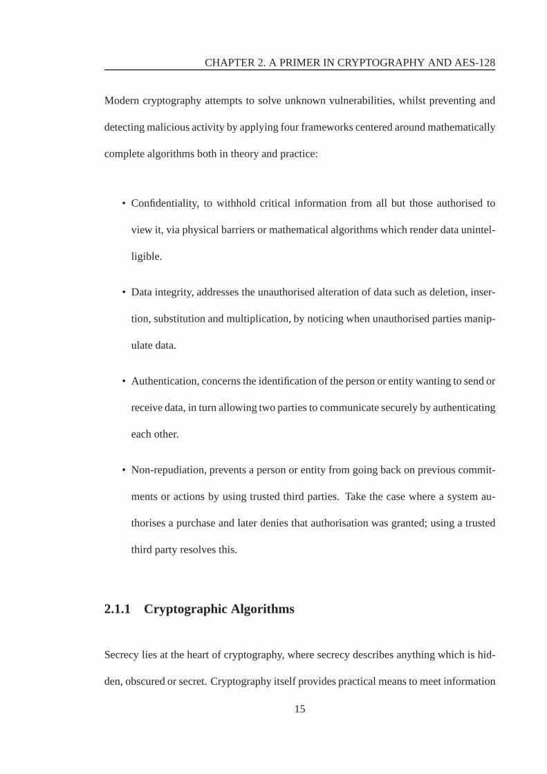
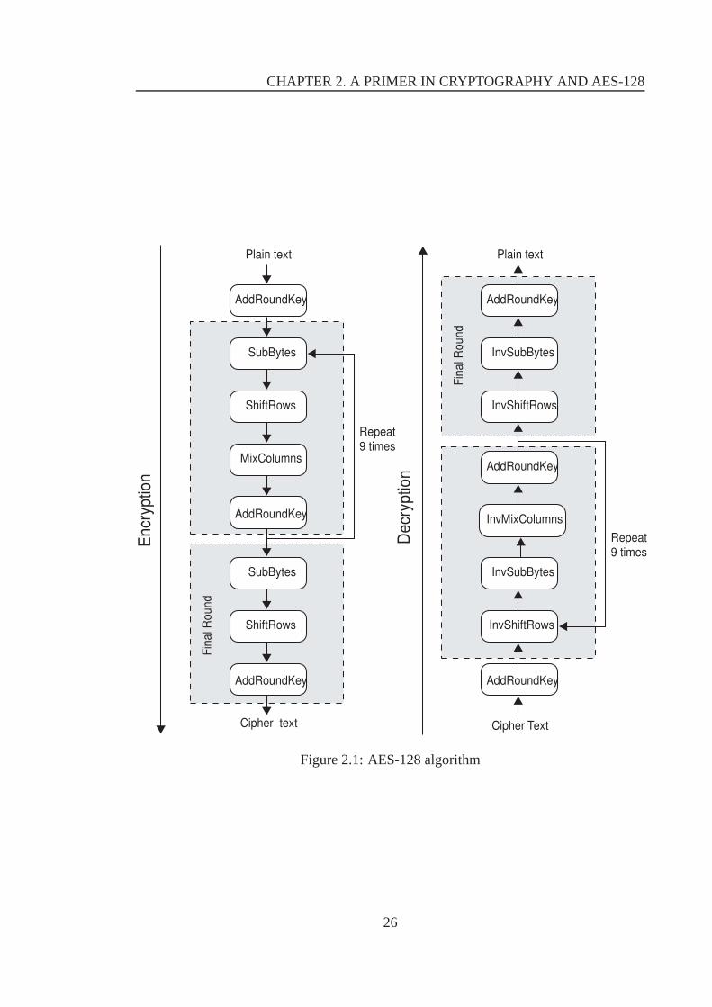
Figure 2.1 illustrates the structure of an AES-128 encryption, where the decryption pro-
cess applies the inverse operations in reverse order. An encryption consists of 10 iter-
ative rounds, the main rounds, each composed of four basic transformationsSubBytes,ShiftRows, MixColumns andAddRoundKey, all operations are defined in terms of arith-
metic in theGF(28). Before the main rounds, an initial round executes featuring anAddRoundKey transformation and followed by a final main round omittingMixColumns.
During each round execution a new key is derived from the initial secret key using a key
schedule.
Data in AES-128 are elements ofGF(28) and represented as polynomials inGF(28) with
coefficients inGF(2), which is equivalent to a byte:
b7 ·x7+b6 ·x6 +b5 ·x5 +b4 ·x4+b3 ·x3+b2 ·x2 +b1 ·x+b0
In this section, juxtaposition is not used and· as in AES specification. For example, the
byte 00000111 corresponds to the polynomialx2 + x+ 1. Using polynomial representa-
tion, addition is the bitwise XOR of two bytes into a new byte polynomial inGF(28). For
example, the hexadecimal addition23+6A = 49 is:
1The original specification by NIST required candidates to support data block sizes of 128, 192 and 256bits. However, the official AES algorithm specification is only defined for 128 bits.
25
CHAPTER 2. A PRIMER IN CRYPTOGRAPHY AND AES-128
Plain text
SubBytes
ShiftRows
MixColumns
AddRoundKey
AddRoundKey
SubBytes
ShiftRows
AddRoundKey
Cipher text
Repeat 9 times
Fin
al R
ou
nd
Plain text
InvSubBytes
InvShiftRows
AddRoundKey
InvMixColumns
AddRoundKey
InvSubBytes
InvShiftRows
AddRoundKey
Cipher Text
Repeat 9 times
Fin
al R
ou
nd
Encr
yptio
n
Decr
yptio
n
Figure 2.1: AES-128 algorithm
26

CHAPTER 2. A PRIMER IN CRYPTOGRAPHY AND AES-128
x5 +x+1 ⊕ x6 +x5 +x3 +x = x6 +x3 +1
Multiplication in GF(28) is modulo an irreducible reducing polynomial of degree 8 used
to define the finite field of AES-128, although different irreducible polynomials could
have been used to constructGF(28), in AES-128 the irreducible field polynomial is
m(x) = 11B = x8 + x4 + x3 + x+ 1. Multiplication equates to multiplication followed
by division using the reducing polynomial as the divisor, where the remainder is the prod-
uct. Besides using polynomials with bit coefficients inGF(2), AES-128 also uses poly-
nomials defined with coefficients inGF(28), when manipulating vectors of four bytes,
corresponds to a polynomial of degree 4:
a3 ·x3+a2 ·x2+a1 ·x+1
In this format, polynomials can again be added by simply XORing the corresponding
coefficients, however multiplication is performed modulo anon-irreducible polynomial
m(x) = x4 +1.
2.3.3 AES-128 Operations
In AES-128, a 4 by 4 byteState matrix constructed in a column like fashion is used to
represent the plaintext. Initially, the matrix holds: the 128 bit plaintext message divided
27

CHAPTER 2. A PRIMER IN CRYPTOGRAPHY AND AES-128
a a a a0,0 0,30,20,1
a1,0
a2,0
a3,0
a1,1
a1,2
a1,3
a2,3
a2,2
a2,1
a3,1
a3,2
a3,3
k k k k0,0 0,30,20,1
k1,0
k2,0
k3,0
k1,1
k1,2
k1,3
k2,3
k2,2
k2,1
k3,1
k3,2
k3,3
Figure 2.2:State andCipherKey matrix
into 16 bytes where each is an element ofGF(28), during encryption the intermediary
results as each round executes, and after encryption the scrambled ciphertext. The actual
bytes are simply mapped into rows and columns: the first byte maps to row 0 and column
0, a0,0, the second byte to row 1 and column 0, and so forth. Similarly, a 4 by 4 byteCipherKey matrix is used to initially hold the secret key and then the new key derived
in each round by the key schedule. Figure 2.2 illustrates thematrices and their respective
mapping.
As mentioned a round is composed of four invertible transformations operating on and
modifying theState matrix. Since each of the four internal functions is invertible de-
cryption merely applies their respective inversions in thereverse direction, excludingAddRoundKey which is its own inverse. The final round omits theMixColumn step.
2.3.3.1 SubBytes
Cryptographic algorithms require non-linear operations to be considered secure. In AES-
128SubBytes, a port-manteau for byte substitution, is the primary non-linear operation.
Its function is to replace each element of theState matrix with values from a 16 by 16
28

CHAPTER 2. A PRIMER IN CRYPTOGRAPHY AND AES-128
a a a a0,0 0,30,20,1
a1,0
a2,0
a3,0
a1,1 1,2
a1,3
a2,3
a2,2
a2,1
a3,1
a3,2
a3,3
b b b b0,0 0,30,20,1
b1,0
b2,0
b3,0
b1,1 1,2
b1,3
b2,3
b2,2
b2,1
b3,1
b3,2
b3,3
a bi,j i,j
S-box
Figure 2.3:SubBytesbyte invertible substitution table (S-Box), as shown in Figure 2.3. The substitution can be
applied directly using a stored S-Box or calculated on demand by:
1. Taking the multiplicative inverse inGF(28)
2. Applying the affine transformation2 overGF(28).
The inverse ofSubBytes is direct byte substitution using the inverse table or by taking
the inverse affine transformation followed by the multiplicative inverse.
2.3.3.2 ShiftRow
TheShiftRow transformation changes the order of bytes of theState matrix, by cycli-
cally shifting each row over different offsets. The first rowis unaffected; the second row
is shifted to the left by one byte; third row by two and the fourth row by three bytes; this
is shown in Figure 2.4.
The inverse ofShiftRow is a cyclic shift of the bottom three rows by 3, 2, 1 respectively,
starting from the bottom.
2An affine transformation between two vector spaces consistsof a linear transformation followed by atranslation.
29

CHAPTER 2. A PRIMER IN CRYPTOGRAPHY AND AES-128
m n o p
h i j k
d e f g
w x y z
m n o p
i j k h
f g d e
z w x y
no shift
cyclic shift by 1
cyclic shift by 2
cyclic shift by 3
Figure 2.4:ShiftRowsa a a a
0,0 0,30,20,1
a1,0
a2,0
a3,0
a1,1 1,2
a1,3
a2,3
a2,2
a2,1
a3,1
a3,2
a3,3
b b b b0,0 0,30,20,1
b1,0
b2,0
b3,0
b1,1 1,2
b1,3
b2,3
b2,2
b2,1
b3,1
b3,2
b3,3
a 1,j
x c(x)
a 2,j
a 0,j
a 3,j
b1,j
b2,j
b0,j
b3,j
Figure 2.5:MixColumns2.3.3.3 MixColumns
In theMixColumns transformation the columns of theState are considered as polynomi-
als overGF(28) and multiplied modulox4 +1 with a fixed polynomial with coefficients
in GF(28) defined as:
c(x) = 03 ·x3+01 ·x2+01 ·x+02
2.3.3.4 AddRoundKey
The AddRoundKey transformation simply XOR’s (adds) the present key stored in theCipherKey matrix, generated by the key schedule, with theState matrix as shown in Fig-
ure 2.6. AES-128 requires 11AddRoundKey operations including the initialAddRoundKey30

CHAPTER 2. A PRIMER IN CRYPTOGRAPHY AND AES-128
a a a a0,0 0,30,20,1
a1,0
a2,0
a3,0
a1,1
a1,2
a1,3
a2,3
a2,2
a2,1
a3,1
a3,2
a3,3
k k k k0,0 0,30,20,1
k1,0
k2,0
k3,0
k1,1
k1,2
k1,3
k2,3
k2,2
k2,1
k3,1
k3,2
k3,3
+ =
b b b b0,0 0,30,20,1
b1,0
b2,0
b3,0
b1,1
b1,2
b1,3
b2,3
b2,2
b2,1
b3,1
b3,2
b3,3
Figure 2.6:AddRoundKeyoperation performed before the mains rounds execute.
2.3.3.5 Key Schedule
The key schedule generates 10 round keys using the initial key as a seed, where each new
round key,nk, is created by manipulating the previous round key stored inCipherKey.
The key schedule for AES-128 is as follows: the first 4 bytes ofCipherKey, k0,0 to
k0,3, are left rotated, then theSubBytes transformation is applied to each byte of the
new matrix. Next, this is XORed with a 1 byte variable,Rcon, representing the round
number padded with 3 bytes of zeros. The obtained word is XORed with the last 4 bytes
of CipherKey, k3,0 to k3,3, in turn producing the last word of the new round keynk3,0
to nk3,3. The second last word of the new round key, bytesnk2,0to nk2,3, is formed by
XORing the word just formed with the second last bytes ofCipherKey k2,0 to k2,3. This
is repeated to form the remaining words of the new round key, which is then stored inCipherKey.
31

CHAPTER 2. A PRIMER IN CRYPTOGRAPHY AND AES-128
2.4 Cryptanalysis Attacks
Cryptographic algorithms are designed to be mathematically secure by cryptographers,
the complementary discipline is cryptanalysis which is used by cryptanalysts and attack-
ers to decipher encrypted information by discovering the secret key; and refers to any
means (attack) to circumvent security by preying on cryptographic weaknesses. In tempo
with the dramatic increases in cryptography and computational power, attributed to the
digital age, the underlying techniques of cryptanalysis have evolved from pen-and-paper
to sophisticated computer-based solutions, one the earliest being the Engima machine
used in World War II. Modern cryptography has become fairly resistant to mathemati-
cally cryptanalysis attacks, although new algorithms are frequently released by academia
and then broken. Likewise, industrial algorithms are just as susceptible, for instance the
protocol, WEP [7], used to secure wireless networks has beenshown to be vulnerable.
In practice, cryptography and the science of cryptanalysisare as important as each other,
because information security has to be guaranteed to the end-user by proving a system
is fool-proof against feasible cryptanalysis attacks. Theactual implications of any given
cryptanalysis attack, rests on how much of a threat it introduces, the majority of which are
theoretical and are only possible in the realm of maths, thusunlikely to be applicable to
real world situations. Regardless, every cryptanalysis attack has to be considered and is
judged on: what knowledge and capabilities are needed as a prerequisite? How much ad-
ditional secret information is deduced? How much effort is required? Attacks can also be
characterised by the amount of resources they require, time(number of operations which
32

CHAPTER 2. A PRIMER IN CRYPTOGRAPHY AND AES-128
need to be performed), memory (storage requirements) and data (quantity of plaintexts
and ciphertexts).
In the future, quantum computing has the potential to conduct extremely fast brute force
key searches, which means key lengths considered beyond an attacker’s resources today
would be become likely. At the moment cryptanalysis attacksfall into three categories:
linear, differential and side-channel. To date the only successful attacks on AES-128 have
been side-channel.
2.4.1 Linear Cryptanalysis
Assuming an attacker has access to a set of plaintexts and thecorresponding ciphertexts,
linear cryptanalysis sets out to take advantage of linear expressions involving plaintext
bits, ciphertext bits and intermediate key bits. The rudimentary idea is to approximate a
portion of the algorithm’s operation with a linear expression, where linearity refers to a
bit wise XOR operation, then determine if the expression hasa high or low probability
of occurring. If the algorithm displays a tendency for a particular expression to hold
with high probability or not to hold this is evidence of weaknesses in the algorithm’s
randomisation abilities, which in turn can be used to break the algorithm.
2.4.2 Differential Cryptanalysis
Differential cryptanalysis attacks are primarily aimed atsymmetric cryptography using
block ciphers and can be summarised as the study of how differences in an input affect
33

CHAPTER 2. A PRIMER IN CRYPTOGRAPHY AND AES-128
the output. In the case of block ciphers, such as AES-128, it is a set of techniques for
tracing non-random behavior during round execution to recover the secret key.
It was first observed by Eli Biham and Adi Shamir, who later published their research
covering a number of attacks against various symmetric block ciphers including theoret-
ical weaknesses in DES [91]. However, it was noted that DES was surprisingly resilient,
indicating perhaps its IBM designers already knew of the potential attack. Since it be-
came public knowledge it has become a basic concern, hence new algorithms are always
accompanied by evidence that the algorithm is resistant.
2.4.3 Side-channel Cryptanalysis
Linear and differential cryptanalysis attacks are based oneither knowing the ciphertext
or plaintext, knowing both, or the ability to define what plaintext is being encrypted.
Both are based on a traditional model that a cryptographic device is an abstract machine
which receives input, plaintext and key, and produces a output, ciphertext. In contrast,
side-channel cryptanalysis, which is usually statistically based, is a relatively new area
of research, escalating since the mid-nineties. It focuseson the physical implementation
of cryptographic algorithms; and exploits the characteristics of integrated circuits which
cause side-channel or information leakage during the operation of the cryptosystem (on
the side) as it interacts and influences its environment. This in turn provides useful and
extra information about secrets in the system, for example,the cryptographic key, partial
state information, full or partial plaintexts and so forth,which can be harnessed statisti-
34

CHAPTER 2. A PRIMER IN CRYPTOGRAPHY AND AES-128
cally or otherwise to break algorithms, deduce secret keys and decipher plaintext. The
term cryptophthora (secret degradation) is sometimes usedto express the degradation of
secret key material resulting from side channel leakage.
Furthermore, devices without protection mechanisms can easily be tampered with, which
allows an attacker to either create new sources of leakage orunintended behaviour; for ex-
ample by injecting logical faults to make transistors causeless switch. The industrial view
is to only make a device secure against attacks pertaining toits application and to gain
certification rather than implementing unnecessary countermeasures that drive up costs.
Most practical solutions rely on increasing the complexityof side channel cryptanaly-
sis, thereby complicating the statistical analysis and increasing the number of readings
necessary to the point where it is infeasible or too expensive to perform. However, the
resources required for side-channel cryptanalysis attacks are relatively low and time has
shown developing effective countermeasures is far from trivial.
2.5 Summary
Cryptography is an important aspect of modern life and has evolved to allow privacy and
safety, by using sophisticated mathematical algorithms which take plaintext data and out-
put meaningless ciphertext. AES-128 has become the new encryption standard of choice,
however all devices are susceptible to cryptanalysis. In particular side-channel cryptanal-
ysis attacks which target the physical implementation rather than the algorithm. This
Chapter has provided a background to cryptography and encryption algorithms, specif-
35

CHAPTER 2. A PRIMER IN CRYPTOGRAPHY AND AES-128
ically the Advanced Encryption Standard required in later Chapters. The last section
introduced the ways in which an attacker can break algorithms using cryptanalysis and
introduced side-channel cryptanalysis.
36

Chapter 3
Power Analysis
This Chapter introduces how CMOS power consumption leaks side-channel information,
power analysis and differential power-balancing. Then themost known and cited counter-
measures from literature are evaluated using SPICE simulations, followed by an overview
of alternative countermeasures.
3.1 Introduction
Power analysis is part of a wide spectrum of side-channel cryptanalysis attacks, yet re-
mains the most compromising, revealing and studied. What can be considered as elemen-
tary power analysis was unveiled to the cryptographic community, little over seven years
ago, by Kocher in his well cited paper [10]. It germinated from a countermeasure de-
signed to prevent timing analysis of RSA and DSS [11] by Kocher, which added dummy
37

CHAPTER 3. POWER ANALYSIS
operations to a smartcard’s encryption algorithm in an attempt to remove timing variations
of operations. However, his experiments revealed the variations not only depend on what
instruction is executed but also significantly on the actualparameters passed, such as, the
secret key, plaintext or intermediary data. For example, a device using ripple-carry addi-
tion will have a very deterministic ADD instruction timing due to binary carries. Kocher
also noticed that the dummy operations consumed differing amounts of power compared
to meaningful operations and duly raised the question: if power is visibly dependent on
operations and operands, do the statistics of a smartcard’spower curve(s) hold more sen-
sitive information, specifically cognating to the secret key? Further investigation and ex-
periments confirmed his ideas and two types of power analysiswere developed. In some
cases a single sampled power curve from a smartcard executing instructions was enough
to reveal relevant information about the secret key, which he termed simple power analy-
sis (SPA). In addition, Kocher claimed as few as 1000 sampledpower curves followed by
statistical analysis using a difference of means hypothesis test, could break most smart-
card’s encryption [10], which he termed differential poweranalysis (DPA). This promptly
drew the attention of both smartcard vendors and the cryptographic community, and even
featured in an article in the New York Times [36].
The potential implications of power analysis have branchedfrom academia to consumers
over time and no more so than from illegally decrypting Satellite TV channels, said to
have originated from South American drug lords who had a personal desire to have Satel-
lite TV wherever they were located, without the risk of signing up to a service. Unsurpris-
ingly, there were no practical limits on equipment costs, time or talent enlisted to decipher
38

CHAPTER 3. POWER ANALYSIS
the channels, and once they had broken the system they had a new business interest cov-
ering their investment. Another example is banking, for instance, imagine a simple and
fictitious current account system, where to increase confidence and to reduce fraud a bank
distributes banking cards embedded with a smartcard chip. Allowing, via cash machines,
account holders are able to access a large proportion of their bank services whenever they
want. Giving the following scenario:
• Alice has a current account which she views as a safe place toput her monthly
salary and presumes only she is able to withdraw money from her account using
her card (the access mechanism).
• Meanwhile Eve makes a living by stealing people’s money using her expertise in
hi-tech fraud where she manipulates bank services.
• The bank has in place a system protecting Alice in case she loses her card, therefore
stopping Eve from withdrawing money from her account even ifshe found the card,
as Alice uses a PIN stored in the card to authenticate herselfto the bank and to
correctly withdraw money she must know the PIN. Without the PIN the card is
useless to Eve.
• Even though the network link between the bank and Alice can be observed or altered
by Eve, the information exchanged between Alice and bank is encrypted using a
secret key known only to Alice and the bank.
• Since there are many customers like Alice the bank decides to use a generic secret
key stored in the card for all customers, and Alice rests assured that if Eve finds the
39

CHAPTER 3. POWER ANALYSIS
card her money is safe.
In this system the surety of Alice’s money relies on various components being used in
combination, and for Eve is defined by the effort and cost required to break the system
and reveal the secret key. From a risk point of view, it is desirable to have a different
secret key for each user or every transaction, in the example, the same secret key is used
by all account holders, hence by using power analysis Eve could extract the secret key
and thus conduct message fraud.
The underlying reasons why power curves are correlated to secret keys is that the instan-
taneous power consumption of a smartcard depends on the data(a function of the secret-
key) manipulated during logical operations due to the physical properties of CMOS logic
and at the lowest level equates to transistors switching. A smartcard’s operation is said to
be data-dependent and to leak information, that is, information is contained in its power
curves statistically correlated to the secret key. The actual side-channels leak not only
through power consumption and timing but also electromagnetic emanations (EM). Us-
ing similar techniques to power analysis, Jean-Jacques Quisquarter and David Samyde
[14] later demonstrated electromagnetic emanations (EM) could also be used, based on
the fact electric current flowing through a conductor induces electromagnetic emanations,
which can be picked up by a coil placed close to a smartcard. The recorded informa-
tion can then also be statistically analysed to reveal useful information. Notably, these
EM side-channels include a higher variety of information and can be applied from a cer-
tain distance. While in 1996, Boneh, DeMillo and Lipton indicated the occurrence of
faults can have severe consequences on the strength of cryptographic schemes [92]. They
40

CHAPTER 3. POWER ANALYSIS
showed that for many digital signature and identification schemes faulty outputs caused
by malfunctioning hardware exposed the secret key stored ina device. These attacks ex-
ploit computational errors introduced during cryptographic operations by tampering with
the device. Usually additional information flow can be caused, if the device returns er-
roneous results or an alternative execution path is entered; for the exploitation of wrong
results, mathematical cryptanalysis is required. Faults are often caused by changing the
voltage, tampering with the clock or by applying radiation.Countermeasures for single
faults are to check the result twice and calculating the reverse result, however these can
not prevent precisely controlled dual or multiple fault injections. The results were par-
ticularly relevant to the design of smartcard systems sincethe small size and intended
use of these devices provide an attacker with the opportunity to induce faults and cause
erroneous outputs.
Over the years it has become increasingly difficult to protect smartcards against power
analysis due to the inherent and leaky properties of CMOS logic. Academia often claims
to have solved or developed a “golden” countermeasure, however in reality industry has
shown such claims are unattainable. Choosing an appropriate countermeasure to power
analysis depends heavily on the economic value of the data and the ability of the attacker,
for example, their knowledge and how readily they have access to the necessary resources.
Relevant publications and literature are far from providing manufacturers with a means
of evaluating attacks and designing sound countermeasures. How to actually determine
or judge the effectiveness of a countermeasure is notoriously difficult [58, 59, 60], de-
veloping countermeasures against power analysis has been an active research area ever
41

CHAPTER 3. POWER ANALYSIS
since their discovery. All try to increase the number of measurements required to reveal
the secret key to a level where it is pointless to perform suchattacks. Countermeasures
are often rated according to their relative effectiveness,for example, a countermeasure
that requires an attacker to perform 2M measurements to be successful will be considered
twice as effective as a countermeasure that requiresM measurements. Kocher reported
three countermeasures to power analysis [10], the first, hiding the information leakage;
the second removing the source data dependency through power-balancing; and the third
by shielding the device; the latter is a packaging solution he quoted as being impractical
due to device costs. The first attempts to reduce the signal-to-noise ratio by increasing
the noise, however with sufficient samples it can be bypassedas the information leakage
is never reduced to zero. The second attempts to remove the data dependency through
power-balancing techniques by also reducing the signal-to-noise ratio, but by reducing
the information leakage (signal) and the focus of this thesis.
3.1.1 Power
Digital circuits consume power whenever they perform computations by drawing current
from the supply and then dissipating energy as heat. Power consumption itself, is a sum
of the power consumption of the individual logic cells making up a given circuit and
depends on the number of logic cells, connections between them and how the circuit is
built. When operating a CMOS circuit uses a constant power supply and input signals to
execute, logic cells process the input signals and draw current from the supply causing
the heat dissipation.
42
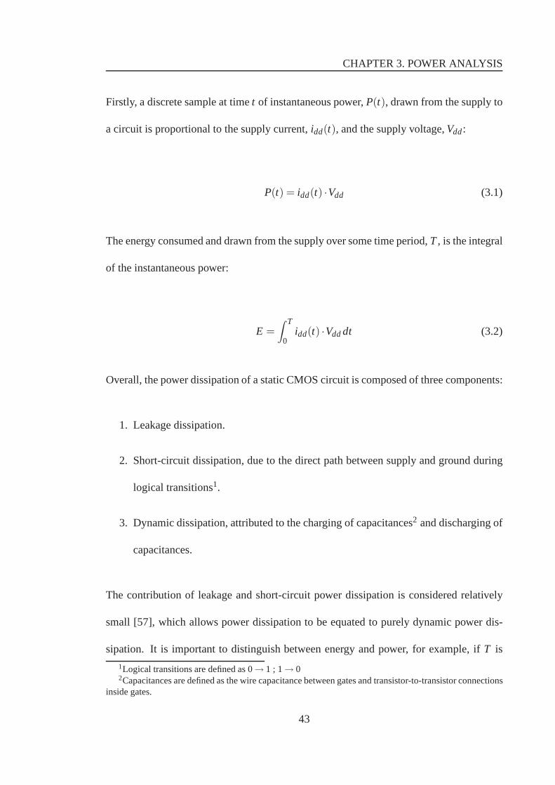
CHAPTER 3. POWER ANALYSIS
Firstly, a discrete sample at timet of instantaneous power,P(t), drawn from the supply to
a circuit is proportional to the supply current,idd(t), and the supply voltage,Vdd:
P(t) = idd(t) ·Vdd (3.1)
The energy consumed and drawn from the supply over some time period,T, is the integral
of the instantaneous power:
E =∫ T
0idd(t) ·Vdddt (3.2)
Overall, the power dissipation of a static CMOS circuit is composed of three components:
1. Leakage dissipation.
2. Short-circuit dissipation, due to the direct path between supply and ground during
logical transitions1.
3. Dynamic dissipation, attributed to the charging of capacitances2 and discharging of
capacitances.
The contribution of leakage and short-circuit power dissipation is considered relatively
small [57], which allows power dissipation to be equated to purely dynamic power dis-
sipation. It is important to distinguish between energy andpower, for example, ifT is
1Logical transitions are defined as 0→ 1 ; 1→ 02Capacitances are defined as the wire capacitance between gates and transistor-to-transistor connections
inside gates.
43
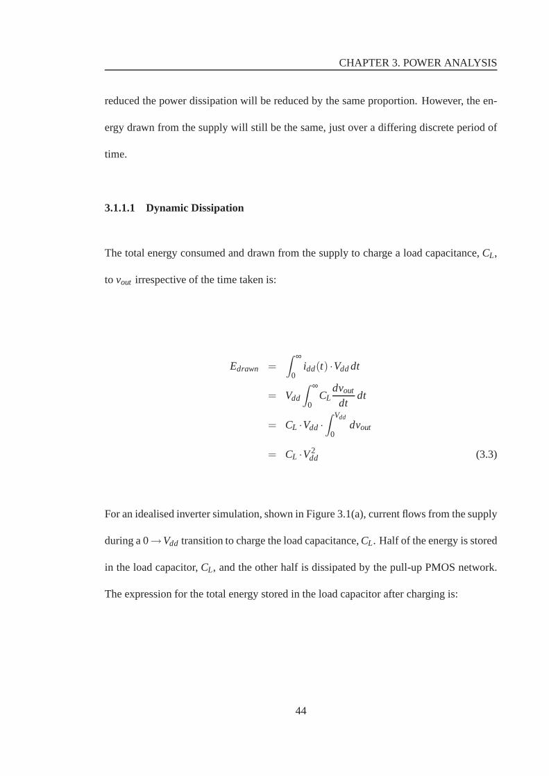
CHAPTER 3. POWER ANALYSIS
reduced the power dissipation will be reduced by the same proportion. However, the en-
ergy drawn from the supply will still be the same, just over a differing discrete period of
time.
3.1.1.1 Dynamic Dissipation
The total energy consumed and drawn from the supply to chargea load capacitance,CL,
to vout irrespective of the time taken is:
Edrawn =
∫ ∞
0idd(t) ·Vdddt
= Vdd
∫ ∞
0CL
dvout
dtdt
= CL ·Vdd ·∫ Vdd
0dvout
= CL ·V2dd (3.3)
For an idealised inverter simulation, shown in Figure 3.1(a), current flows from the supply
during a 0→Vdd transition to charge the load capacitance,CL. Half of the energy is stored
in the load capacitor,CL, and the other half is dissipated by the pull-up PMOS network.
The expression for the total energy stored in the load capacitor after charging is:
44

CHAPTER 3. POWER ANALYSIS
A Q
I
CL
dd
(a) Circuit diagram
time (ns)
Q (V)
A (V)
10.0
Idd (uA)0
150
-150
0.0
4.0
0.0
4.0
0 7.52.5 5.0
(b) Simulation
Figure 3.1: Inverter
Eload =
∫ ∞
0idd(t) ·voutdt
=∫ ∞
0CL
dvout
dtvout dt
= CL
∫ Vdd
0vout dvout
=12·CL ·V2
dd (3.4)
During a discharging transitionVdd → 0 current flows from the load to ground and the
energy stored in the load capacitor is dissipated by the pull-down NMOS network and no
energy is drawn from the supply; in one complete charge/discharge cycle, a total charge of
45

CHAPTER 3. POWER ANALYSIS
Q = CL ·Vdd is transferred fromVdd to ground. The waveform foridd(t) generated using
SPICE simulation is pictured in Figure 3.1(b)3. In summary, each switching cycle takes a
fixed amount of energy equal toCL ·V2dd.
The inverter’s average dynamic power consumption over sometime period,T, is the
integral of the instantaneous power multiplied by its switching frequency,f , of 0→ Vdd
transitions:
Pdynamic =1T
∫ T
0idd(t) ·Vdddt
=Vdd
T
∫ T
0idd(t)dt
= CL · f ·V2dd (3.5)
Example values of energy and power can now be readily calculated, if the load capacitance
is equal to 0.1pF for a supply voltage of 3.3V, the amount of energy needed to charge
and discharge the load is 1.089pJ, and if the inverter is switched at the hypothetical rate
of 1ns, giving a cycle time of 2ns, the average dynamic power dissipation is 0.5445mW.
3Dynamic power consumption is also composed of a constant short circuit current effect, caused bya temporary short circuit whenever the input switches making both transistors conduct. This has beensubtracted fromidd(t) to illustrate the charging and discharging ofCL.
46

CHAPTER 3. POWER ANALYSIS
3.1.2 Switching Activity
Apart from inverters other CMOS gates and networks of interconnected gates have
markedly different switching properties. Their dynamic power dissipation is composed of
two components: the internal power4, Pinternal, and the capacitive load power,Pload; in the
case of the inverter the load power is equivalent to the dynamic power. Furthermore, they
exhibit “lazy switching” characteristics causing a memoryeffect, where the logical values
of outputs are retained from earlier computation cycles. These memory effects, make the
outputs statistically correlated to the inputs, thus data-dependent, and occur when a gate’s
output computes to the same logical value as the existing output; this naturally happens
when more than one set of inputs maps to the same outputs.
Similarly, internal nodes exhibit such memory effects and will discharge or charge deter-
ministically. For example, consider the 2-input NAND shownin Figure 3.2, where two
PMOS transistors connect in parallel and two NMOS transistors connect in series to form
the internal transistor-to-transistor nodeN1. Assume the existing output value is a logical
one andN1 is discharged (the inputs are either 00 or 01); if in the nextcycle AB equal
to 00 or 01 arrives, then the output will retain its existing value and no power will be
consumed. Contrastingly, if in the next cycleAB equals 10 the output will still retain its
existing value, however,N1 will charge, meaningN1 can freely discharge at any point in
subsequent cycles.
The power consumption of complex gates and networks of interconnected gates can only
4The power dissipated by the internal capacitive transistor-to-transistor nodes, also know as intrinsiccapacitances.
47

CHAPTER 3. POWER ANALYSIS
A
Q
B
A
B
N1
Figure 3.2: NAND gate
be truly estimated by taking into account switching statistics, which also highlight mem-
ory effects. For instance, from the truth table of the NAND gate the probability that the
output is at one,P1, is 3/4 and that it is at zero,P0, is 1/4. The probability of a tran-
sition which draws energy from the supply to charge the output from zero to one,P0→1,
is computed by multiplying the two probabilities,P0 ·P1 = 3/16, assuming the inputs are
uniformly distributed. Therefore the probability of discharge,P1→0, is computed by multi-
plying the two probabilities and subtracting them from one,1−P0 ·P1 = 1−P0→1 = 3/16,
and when an output could exhibit a memory effect for the NAND gate. Either way the
switching characteristics of the outputs are statistically correlated to the inputs. Note,
when gates are connected in a network the probabilities are no longer equi-probable, in
this case the probability at the outputs depends on the probabilities of transitions at the
primary inputs.
To calculate the power consumption the concept of switchingactivity is used to determine
the probability of an output switching. ForN periods of 0→Vdd andVdd → 0 transitions,
the switching activity,α, determines how many 0→Vdd transitions occur. In other words,
α represents the probability that a 0→ Vdd transition will occur during the period off .
Hence, the dynamic load power (average) of a complex gate is:
48

CHAPTER 3. POWER ANALYSIS
Pload = α ·C · f ·V2dd (3.6)
The internal power consumption, due to internal capacitivetransistor-to-transistor nodes,
is given by:
Pinternal =n
∑i=1
αi ·Ci ·Vi ·Vdd · f (3.7)
wheren is the number of internal nodes,αi , is the switching activity of each nodei, Ci , is
the capacitance of the internal node, andVi is the internal voltage swing of each nodei.
Note that the internal voltage swing can be different thanVdd. Hence the overall dynamic
power is:
Pdynamic= Pload+Pinternal (3.8)
3.1.3 Timing
Circuits experience various propagation delays and timingphenomenon. A widely
known, and often attributed to up to 20% of the dynamic power dissipated [57], timing
phenomenon is glitching. This occurs in the time period between the start of a computa-
tion cycle and an output settling to its correct value; during this time an output or internal
node may experience spurious transition with voltage levels ranging from 0 toVdd. It
49

CHAPTER 3. POWER ANALYSIS
usually happens, for instance, when the input,a, of a gate,G, arrives earlier than its other
input, b, during a computation,F0. The consequence of such a delay between the input
signals arriving and transitioning is that the output,q, can switch more than once in one
cycle: the output switches whena arrives and again whenb arrives. It should be noted that
during the time span between the arrival of the two input signalsa andb the outputq of
G switches to an incorrect value. Andq is also the input of another logic gate, which will
react to a transition at its inputs and may change its outputsaccordingly; thus incorrect
values can propagate causing more spurious transitions.
Another significant timing phenomenon CMOS circuits exhibit occurs when intercon-
nected gates interact and is mainly due to the topological structure of gates; typically
logical functions are realised by connecting multiple gates in intersecting cones to form
the primary outputs. Since CMOS gates can switch their outputs before all inputs have
arrived, apart from glitching effects, this creates a timing effect5 as outputs can be deter-
mined without necessarily having knowledge of all the inputs. Hence, a gate can propa-
gate it’s output value without having to wait for all inputs to arrive. Consider a NAND
gate, its output will be a logical one whenever one of the inputs is a logical zero. There-
fore, as soon as a logical zero is observed at one of its inputsthe output is uniquely
determined making the rest of the inputs redundant. The topology of the NAND allows
this timing effect and can be seen in the pull-up PMOS networkdue to the parallel ar-
rangement of the PMOS transistors: the output will be pulledhigh when at least one of
the inputs is low, regardless of the other value.
5This timing effect has also been termed temporal timing in [61], early output in [63], early propagationor evaluation in [88] and often in asynchronous publications weak indication.
50

CHAPTER 3. POWER ANALYSIS
3.1.4 Instantaneous Power
Taking timing and switching effects into account a model of instantaneous power can be
developed [45]. In general, almost all computation cycles are initiated by new inputs
and a synchronisation signal, which then triggers a sequence of switching events bringing
a device into its next logical state. A switching event is defined as a capacitive load
charging and drawing energy from the supply. The amount of energy drawn by a particular
switching event distinguishes one from another, while the probability of which switching
events occur and at what point in time they happen depends on both physical, previous
cycles and environmental factors. Overall, the timing and which switching events occur
dictates how energy is drawn over time and instantaneous power values; instantaneous
power can be considered as a sum of all the switching events that take place at timet.
Mathematically, letE be the set of all possible switching events ande be e∈ E. Let
occurs(e, t) be a binary function, returning 1 ife occurs at timet otherwise 0. LetF(e, t)
denote the magnitude for switching evente at timet. Therefore the instantaneous power
value at timet can be modeled as [45]:
P(t) = ∑e∈E
F(e, t) ·occurs(e, t) (3.9)
51

CHAPTER 3. POWER ANALYSIS
3.2 Simple Power Analysis
In [10] Kocher et al. use Simple Power Analysis (SPA) to deduce the example smart-
card’s secret key and as a preliminary step before DPA. They characterise it as: “SPA is a
technique that involves directly interpreting power consumption measurements collected
during cryptographic operations”; in other words the attacker tries to derive the key more
or less directly given a small number of power curves. The attack is performed by exam-
ining the characteristics of a single power curve, often a single power curve is replaced
with the average of a number of curves in order to reduce noise, from here an adversary
can potentially determine [10]:
• The algorithm being used, for instance, if an attacker observed a stream of of XOR
instructions followed by SHIFT instructions on a smartcardrunning AES-128, this
may suggest the start of a round had been identified, i.e.AddRoundKey. Specific
instructions can be identified as they have a unique templatepower signature that
distinguishes them from other instructions.
• Information about the datapath, whether instructions arebeing executed and which
those are, or if dedicated logic is being used.
• Instruction operands and possibly the inputs of dedicatedlogic.
• Sensitive operations (DES operations identified in [10] and applicable to other al-
gorithms include: key scheduling, permutations and comparisons) and synchroni-
sation points for DPA.
52

CHAPTER 3. POWER ANALYSIS
• Hamming weight information.
Since every algorithm that runs on a cryptographic device isexecuted in a sequential
manner, for example in AES-128AddRoundKey is performed before the main rounds,
this leads to a characteristic pattern in the power curve.
The original publication by Kocher [10] documenting power analysis demonstrated SPA
by attacking a common smartcard running the DES algorithm. All 16 rounds were imme-
diately apparent from the smartcards power curve, shown in Figure 3.3(a) for reference.
Even at this granularity the extent of the information leakage is obvious and further anal-
ysis revealed the various rotations used in the DES key schedule. The left-hand arrow in
Figure 3.3(b) shows one rotation in round two and the right-hand arrows two rotations
being performed in round 3. An even closer analysis, enabledKocher to distinguish the
sequence of operations being executed and therefore the means to break the algorithm.
In addition, to exploiting the characteristic power signature of operations, hamming
weight information of operations can be harnessed also. In atypical smartcard a large
proportion of the power consumed has been shown by Messergeset al. in [38] to be due
to internal buses; who concluded, in this instance, there are two types of hamming weight
information an attacker can use:
• Hamming weight correlation information, occurring when the power consumption
and the number of 1’s written on a bus are directly correlated.
• Transition count correlation information, occurring when the power consumption
53

CHAPTER 3. POWER ANALYSIS
and the number of bits that change on a bus are correlated i.e.the hamming weight
of the current and previous value on the bus.
They showed either of the above could be used along with knowledge of the implemen-
tation to reduce the search space of a brute force attack, specifically DES. They further
explained how SPA could be mounted if only transition count information is available,
by knowing what was on the data bus before and after a computation cycle. An example
where this is possible, is when a pre-charged bus is used, here, the number of transitions
to zero will interrelate to the height of the power curve [38].
The success of SPA and what is revealed really hinges on the manner in which an algo-
rithm is implemented. For example, a dedicated hardware implementation of AES-128
incorporating a lot of parallelism or novel techniques willobviously make an SPA attack
significantly harder. Contrastingly, if the algorithm has been coded as-is, it predictably
will reveal a great deal of information and increase the success of the attack.
3.3 Differential Power Analysis
Differential Power Analysis (DPA) [10] builds on the visible variations attackers can use
to gain useful information by using more subtle informationabout a secret key’s identity
hiding in a smartcard’s power curve. Like SPA, DPA exploits the characteristic behavior
and interactions of transistors, however, in such a fashionthat it can extract specific infor-
mation correlated to the secret key. The essential difference being, statistical analysis is
54

CHAPTER 3. POWER ANALYSIS
(a)
(b)
Figure 3.3: SPA on DES rounds
used to isolate small differences in power consumption, to determine whether a guess on
a particular byte of the secret key (subkey),Kn, is correct or not; the overall objective is to
recover the complete secret key in a byte-by-byte divide andconquer manner. In the case
of AES-128, 16 subkeys form the 128-bit secret key, thus the attack has to be performed
16 times to reconstruct the full key.
From a theoretical position, for a successful DPA attack theso-called fundamental hy-
pothesis must be satisfied [44], that is: a variable must be calculated at some point, which
will allow an attacker to decide whether certain inputs or outputs give the same variable
result or not. In other words, the outcome or success of such an attack is based on the
condition that an encryption variable is calculated whose value is dependent upon a sub-
set of the secret key and upon known plaintext or ciphertexts. What makes the attack
55

CHAPTER 3. POWER ANALYSIS
particularly interesting and powerful is most cryptographic algorithms satisfy the funda-
mental hypothesis [10]. On a practical front, Kocher’s ending and resounding note about
DPA in [10] was how the whole process is easy to implement, only requires standard lab
equipment and is easily automated.
The attack begins by applyingN plaintexts to the smartcard under attack while it encrypts
using the unknown secret key. For each of theN plaintext inputs,PTIi, a set,Ω, of discrete
power curves,Si j , are recorded via the high-speed analog-to-digital converters commonly
found in digital oscilloscopes; where thei index corresponds to a particular power curve
and its accompanying plaintext and thej index corresponds to a given sample’s time.
The attacker begins the analysis stage by choosing: a targetbit to attack; a subkey hypoth-
esis,Ks; and an appropriate selection function,D, which takes plaintext and the subkey
hypothesis as inputs. The selection function is picked so atsome point its value is calcu-
lated in order to satisfy the fundamental hypothesis. When this occurs there will be slight
differences in the power consumed between power curves.
Next, on the basis of the hypothesis the captured power curves are partitioned into two
setsA andB such thatΩ = A⋃
B and|A|+ |B|= N. If the value of the target bit is zero for
a particular power curve,D = 0, it is classified toB and if it is one,D = 1, intoA, which
can be stated formally as:
A = Si j ∈ Ω : D() = 1andB = Si j ∈ Ω : D() = 0
A widely used selection function is modulo addition (XORing), which occurs frequently
56

CHAPTER 3. POWER ANALYSIS
in cryptographic algorithms, between the secret key or derived key and plaintext or in-
termediate ciphertext; in AES-128 this equates to theAddRoundKey function. If an 8 bit
selection function,D(Ks,PTIi) = KsxorPTIi , is chosen, any of the 8 bits ofD would be
available as the target bits. If bit zero is chosen the power curves would be partitioned, on
the basis of the subkey hypothesis, according to whether bitzero was a logical 0 or 1.
The final step is to compute the “difference of mean” of the twosets by subtracting the
average of each set, to form what Kocher called a differential trace [10],DT[ j], formally:
A0[ j] =1|B| ∑
Si j∈B
A1[ j] =1|A| ∑
Si j∈A
DT[ j] = A0[ j]−A1[ j]
If the subkey hypothesis,Ks, was correctKs = Kn, the differential trace will be statistically
correlated to the secret key and will show noticeable power bias spikes atj points in time,
where power variations occurred satisfying the fundamental hypothesis, hence:
1|A| ∑
Si j∈S1
6= 1|B| ∑
Si j∈S0
57

CHAPTER 3. POWER ANALYSIS
And DT[ j] = ε will be true, whereε represents the differential curve statistically corre-
lated to the subkey, the correct hypothesis ofKs.
If the hypothesis is incorrect then:
1|A| ∑
Si j∈S1
=1|B| ∑
Si j∈S0
ThusDT[ j] = 0 will be true instead, meaning the criteria used to separatethe subsets will
be approximately random. If a random function is used to divide a set into two subsets, the
difference in the averages of the subsets should approach zero as the subset sizes approach
infinity [10], as any randomly chosen subset of a sufficientlylarge data set will have the
same average as the main set. As a result, the difference willbe effectively zero at all
points, in this case the attacker has to repeat the process using a new subkey hypothesis.
In practice, a differential trace matrix is constructed of all potential 256 subkeys and then
superimposed, typically a given differential trace might not be completely flat. Once
the attacker has confirmed whether a subkey is correct the whole process is repeated to
crack the next subkey until the entire key is known, in turn eventually breaking the entire
encryption algorithm. Figure 3.4 highlights DPA figuratively and applicable to AES-128
for an arbitrary selection function.
Related to the principles of how power is consumed by CMOS logic and its timing ef-
fects presented earlier, it is clear that power analysis could harness any form of leakage
using the same principles. From the fact transitions are affiliated and determined by the
statistical phenomenon of gate inputs and previous outputs, to the differing way energy
58

CHAPTER 3. POWER ANALYSIS
N plaintexts Secret Key
Device Under Attack
Collect Power Curves
Partition Curves 8 bit Subkey
Generate
Differential Trace
Superimpose
Differential Trace
Identify Power
Bias Spikes
Secret Key
Repeat
256 timesRepeat
16 times
Figure 3.4: DPA flowchart
59

CHAPTER 3. POWER ANALYSIS
is consumed between a 0→ Vdd andVdd → 0 transition, for example hamming weight
information or timing variations or glitches and so on, which all lead to a statistical corre-
lation between the subsets. Unfortunately, a modern smartcard will contain thousands of
CMOS gates exhibiting data-dependent effects resulting ininformation leakage correlated
to the secret key, which can be exploited using either simplepower analysis or differential
power analysis.
The power model also captures how energy is drawn from the supply and which switching
events occur, their magnitude and timing. For example, ifP1 andP2 are two power curves
generated from different inputs to the same logic network, it is likely, that how energy is
drawn over time will be different forP1 than it is forP2, thus an instantaneous power
value (sample) at timet from the two curves will be different. If the same sequence
of switching events occurred in each computation cycle, regardless of processing done
in earlier cycles, thenP1 andP2 would then be the same, thus all instantaneous power
samples the same. Therefore this means all the differentialtraces created for any subkey
hypothesis would be zero and the correct differential tracewould show no power bias
spikes and DPA would not be possible.
3.3.1 Power Bias Spikes
DPA tries to deduce the correct subkey hypothesis by formingall possible differential
traces and looking for noticeable peaks, however, noise components which are sufficiently
random and not canceled during partitioning may potentially mask the power bias spikes
60

CHAPTER 3. POWER ANALYSIS
[10]. The number of power curves,N, in reality required to practically perform a success-
ful DPA attack, heavily depends on the noise in the measurements,σ , and on the size of
the power bias spikes atj points inε. If the power bias spikes are relatively small and for
example the smartcard contains a random number generator the subkey hypothesis may
be guessed incorrectly or not at all. The power bias spikes can typically be identified if
[38]:
ε >2σ√
N
Therefore, the number of power curves necessary for the attack is:
N > (2σε
)2
Messerges [38] suggested, initially, an easy way to decrease N would be to use multiple-
bit DPA attacks by showing the magnitude of the power bias spikes depends on the num-
ber of bits used in the selection function, hence a multiple bit attack would increase the
magnitude of the power bias spikes inε. Such an attack differs to DPA in that three sets
are used instead of two during partitioning, the extra set holds the power curves not cov-
ered by the selection function. For example, in the 4-bit attack on DES in [38] the power
traces are partitioned according to whether the selection function is 0000 or 1111, giving a
expected four fold increase in the power bias spikes inε; the third set holds values which
are not 0000 or 1111. The main issue Messerges’s realised waspotentially higher levels
61

CHAPTER 3. POWER ANALYSIS
of noise would be present than in ordinary DPA, as less power curves would be distributed
across three subsets instead of two. Hence the averages could have higher levels of noise
even though the power bias spikes should have a greater magnitude, the experiments later
in [38] showed that this introduces difficulties in recognising the power bias spikes of the
correct guess from the incorrect guess. Overall their conclusion was when mounting a n-
bit attack the attack may actually need more power curves to reduce the noise to sensible
levels and more computational power, implying an attacker cannot arbitrarily increase the
number of attack bits due to the spread of the power curves across the subsets.
3.3.2 Higher-order DPA attacks
Since the first publication [10] documenting power analysisattacks a number of higher-
order or n-order extensions have been proposed to increase the statistical might of the
original attack. In this context, standard DPA is referred to as first-order DPA and partic-
ularly impressive considering relatively simple mathematics can potentially, indeed with
a degree of certainty, reveal the secret key. Higher-order DPA attacks were also described
alongside first-order DPA in [10], Kocher defined them as first-order DPA attacks which
use one or more samples within a single power curve by applying joint statistics, i.e. by
using more than one selection function; whereas first-orderDPA calculates the statistical
properties of each power curve at each sample point.
Another definition of higher-order DPA attacks [39], stateshigh-order DPA attacks as
making use ofn different samples in the power curve that correspond ton different inter-
62

CHAPTER 3. POWER ANALYSIS
mediate variables calculated during the execution of the algorithm. In higher-order DPA
attacks the fundamental hypothesis given in [40] is that: there exists a set ofn interme-
diate variables, that appear during the computation of the algorithm, such that knowing
a few key bits (in practice less than 32 bits) allows the attacker to decide whether two
inputs (respectively two outputs) give or not the same valuefor a known function of these
n variables.
Chari et al. [45] showed that the complexity of performing higher-order DPA increases
with the exponent of the number of points used when applying joint statistics. And,
in practice, higher-order DPA attacks are more difficult to mount than first-order DPA
attacks due to more complex analysis, increased memory or processing requirements and
an increased number of power curve patterns [41].
3.3.3 Variations of DPA
Both first order DPA and higher order DPA require the attackerto know all the plain-text
or all the cipher text information. Biham and Shamir [42] cited this fact as one of the main
disadvantages of DPA when the exact values of the plaintext or ciphertext are unknown,
which is plausible if a device is using many layers of security. In this instance, they
suggested applying DPA to an algorithm’s key schedule, specifically AES-128, where
knowledge of plaintext nor ciphertext information is required. The AES-128 key schedule
is obviously a natural choice as its power consumption is always only a function of the
secret key.
63

CHAPTER 3. POWER ANALYSIS
The first part of the attack, as discussed in [42], is to discover the portion of the power
curves corresponding to the key schedule by executing the algorithm many times and
comparing the aligned power curves. Once this is achieved, the clock cycles which show
large variations in power consumption are eliminated from further consideration. The re-
maining clock cycles represent operations that are theoretically independent of operations
using plaintext or ciphertext, and from here statistical analysis can be conducted. The at-
tack from the outset is somewhat inhibited, for example in smartcards where the AES-128
key schedule executes in parallel with the rounds, thus isolating the key schedule is im-
possible due to concurrency. Clavier et al. [46] also proposed an improvement to general
DPA called Hamming integration.
3.3.4 Conducting DPA
From both an experimental point of view and an attackers, to successfully conduct a power
analysis attack it is necessary to be able to definitively measure power consumption. A
typical measurement setup consists of the cryptographic device under attack, a power sup-
ply circuit, a power measurement circuit, a digital oscilloscope and PC. The cryptographic
device uses an interface to communicate with its environment; the power supply circuit6
provides power to the device and other circuit components; the power measurement cir-
cuit is inserted between the power supply and device under attack to directly measure
the power consumption; the digital oscilloscope samples the signal which is provided by
the measurement circuit; and the PC coordinates the environment and controls the device
6Two power supplies of differing voltages are often required.
64

CHAPTER 3. POWER ANALYSIS
under attack.
Digital oscilloscopes by definition measure the voltage of signals, therefore to measure
power and current consumption it is necessary to generate proportional voltage signals to
represent them. For power analysis this is done by insertinga small resistor inline with
the power supply ground and device ground forming the measurement circuit; typical
values range from 1Ω to 50Ω. The voltage drop across the resistor is proportional to the
current flowing to the device, and assuming the voltage is constant the voltage drop is also
proportional to the power consumption. The sampled signal is inherently analogue and
converted to a digital form by the scope, as such care should be taken when choosing a
suitable oscilloscope.
3.4 Power-balancing
In [10] Kocher suggested, and is also intuitively apparent,that the most effective power
analysis countermeasure is outright prevention. Other countermeasures endeavor to re-
duce the signal-to-noise ratio by maximising the noise aspect so as to camouflage the fun-
damental causes. An interesting alternative, or in addition to other countermeasures, is
to span the logic and physical levels of the abstraction pyramid and use power-balancing,
a form of differential logic which returns to a fixed state after every computation, to re-
duce the information leakage moreover the signal aspect of the signal-to-noise ratio. The
switching activity of which, at the logic level, becomes predictable and glitch free to give
gate outputs a 100% switching factor (balanced hamming weight), this means that the
65

CHAPTER 3. POWER ANALYSIS
switching activity,α, is a constant opposed to a meandering value on every computation
cycle. It follows, in relation to the power model, if the physical implementation of such
a logic style guarantees that all switching events, and not only for gate outputs, are the
same in magnitude and timing in every computation cycle, thus solving the fundamental
causes, power analysis will be theoretically prevented.
A logic style denoted as differential has two defining characteristics, firstly all binary
interconnect values (wires), here represented byA, are defined by both their true and
complement:A andA; whereas regular CMOS represents binary values using one wire,
differential logic uses two wires to express one bit of data.Algebraically, the possible
binary values ofA, 1 and 0 respectively, areAA and AA, which map to the code-word
subset of binary states10, 01 from the set of possible states00, 01, 10, 11. Secondly,
a meaningless “fixed state” is always used between cycles of computation to separate the
meaningful transitions to and from code-words, even if the same code-word occurs in the
next cycle. The two states available to take on this role are 00 or 11, whichever is chosen
there is always a deterministic order of switching from a code-word cycle to a fixed state
cycle to a code-word cycle, and so on, regardless of a gate’s input sequence or the primary
inputs values. The fixed state has various names in different, but overlapping, spheres of
electronics. In dynamic logic, it is analogous to pre-charging where a gate’s operation is
divided into two cycles: the two outputs of a gate are charged, then during evaluation one
is discharged to form a code-word. In the asynchronous community, differential logic is is
commonly referred to as return-to-spacer dual-rail or having a 1-of-2 encoding; the fixed
state as a spacer or NULL state; and the deterministic order of switching as a protocol.
66

CHAPTER 3. POWER ANALYSIS
A_1 Q_1
A_0 Q_0
Idd_1
Idd_0
(a) Circuit diagram
0
time (ns)
8.06.04.02.0
0
150
0
150
0
150
0.0
4.0
4.0
0.0
Idd_total (uA)
Idd_1 (uA)
Idd_0 (uA)
Q_1 (V)
Q_0 (V)
time (ns)
(b) Simulation
Figure 3.5: Two inverters switching through code-words to fixed state
67

CHAPTER 3. POWER ANALYSIS
The immediate advantages of using a power-balanced logic style can be better understood
by considering an example of two inverters transitioning through two ’code-word to fixed-
state’ cycles7 as shown in Figure 3.5(a) and (b). For each transition to a code-word, the
same energy is drawn from the supply by the inverter that switches in Figure 3.5(a). The
current consumption of the individual inverters are shown below the output voltage wave-
forms,Idd_0andIdd_1, in Figure 3.5(b) and summed in the lowest waveform,Idd_total,
in Figure 3.5(b). The example also highlights the aspects ofthe physical level for power-
balancing, in so much as that at the logical level a differential logic style only guarantees a
constant switching activity and glitch free operation and not necessarily constant timing.
Hence, the increase in security is reliant on both levels. Inthe example above the arrival
of the code-words and capacitances is constant and no internal nodes are present.
Security publications regularly forget to mention the physical side of a differential power-
balancing scheme. One of the main security aspects which have to be addressed at the
physical level when using a power balanced logic style is ensuring the capacitances are
equal, however physical routers act contrary to this to minimise crosstalk. Modern tools,
use a grid based system, which have been manipulated in [64] for differential routing.
Place and route proceeds using fat wires and which are then transformed into the final
differential design by parsing the design database and reading in the differential rules.
The method requires manipulating design rules and redefining the layout interfaces (ab-
stracts), this may have certain implications since these are the property of the foundry
and cited as being a sub-optimal scheme in [33] and having cross talk issues. Another
7Since inverters are used, 11 is applied as the fixed-state to the inputs to generate a 00 fixed state outputand the applied codewords are inverted.
68

CHAPTER 3. POWER ANALYSIS
method, the backend duplication method [65], and quoted as having similar problems in
[66], attempts to implement balanced routing independently of the differential logic style.
Firstly database descriptions of the cells are modified to implement a compatible inter-
face and a symmetric layout structure, while place and routeproceeds by placing cells
on every other row and constraining the router vertically toleave empty channels so that
everything can be duplicated later. After the first routing pass all the cells are duplicated
onto the empty and adjacent rows, while the routing is shifted horizontally into the empty
vertical channels. Bouesse et al in [67] used an iterative design to balanced pairs by col-
lecting parasitic information after every routing. Experiments have shown a similar best
effort approach is, in reality, only feasible when designing an actual ASIC which is to
be sent for fabrication. The parasitics of the two wires forming a differential pair can be
analysed by extracting a list of capacitances followed by simple file processing to com-
pute the imbalance between the wires. The increase in security can be assessed by the
ratio of the wire’s routing capacitanceC(true)/C( f alse) [65, 67].
3.4.1 Power-balancing Countermeasures
The main differential countermeasures are described and resistance to power analysis
analysed in this section; the latter part separately discusses their relative design proper-
ties. The first differential power-balancing countermeasure (DIMS_1) proposed by Moore
et al. in [34] and demonstrated in a prototype chip, used Delay Insensitive Min-term Syn-
thesis [70] (DIMS) logic returning to a 00 fixed-state (all-zeroes); and built from standard
cells for use in either a clocked or clockless environment. In this context, returning to the
69

CHAPTER 3. POWER ANALYSIS
fixed state is known as the logic’s protocol and the logic is said to “return-to-spacer” after
a code-word cycle. Previously DIMS logic had only been used in clockless designs due
its inherent synchronisation properties; [71] also reported a clockless chip using DIMS
logic.
An actual differential function or gate is formed by implementing explicitly the boolean
function using a C-element for each min-term and OR gates forthe ORing of the
minterms. For example, a DIMS NAND gate is shown in Figure 3.6(a) and implements
the Boolean functions in Equation 3.10 and 3.11:
Q1 = a0 ·b0+a1 ·b0+a0 ·b1 (3.10)
Q0 = a1 ·b1 (3.11)
The first level of C-elements8 ensures an output is only generated when both inputs have
arrived by synchronising the arrival of the primary inputs.However, the logic depth ofQ1
is uneven compared toQ0 giving rise to data-dependent behavior: a temporal timing effect
and a different number of switching events between the two paths. Since the solution uses
standard cells the power-balancing is limited to the logical level, hence the underlying
transistor implementation will also exhibit data dependent behavior.
A logic style’s resistance to power analysis can be evaluated by constructing a differential
trace using SPICE simulation [33]. According to DPA, power curves are generated for the
8A C-element holds its present output, unless a 00 or 11 are present on its inputs, which give a binary 0and 1 respectively.
70

CHAPTER 3. POWER ANALYSIS
C
C
C
C
Q1
Q0
A 0A 1B0B1
Synchronisation
(a)
0 0.20 0.40 0.60 0.80 1.00 1.20100
50
0
50
100
150
200
Time (nS)
Diff
eren
tial T
race
(uA
)
(b)
Figure 3.6: DIMS_1 NAND and differential trace
gate in question and separated into two subsets: where an output computes to a binary 1
and 0. The two subsets are then averaged and subtracted to form the differential trace.
Figure 3.6(b) shows the differential trace for the DIMS_1 NAND gate, where majority
gates were used for the C-elements and twenty input combinations used, covering all
input combinations, arriving randomly. A noticeable powerbias spike can be observed,
peaking at 170µA and present for 0.50ns, and acts to quantify the information leakage and
demonstrates the extent of data dependent operation still present due to using standard
cells and unsymmetric paths.
To balance the paths and to implement fault propagation which uses the 11 fixed state
Moore et al. added extra logic (DIMS_2) toQ0 forming the Equation 3.12 and illus-
trated in Figure 3.7(a); the new differential trace peaks at90µA and present for 0.27ns,
Figure 3.7(b).
Q0 = a1 ·b1+a0 ·a1+b0 ·b1 (3.12)
71

CHAPTER 3. POWER ANALYSIS
C
C
C
Q0
Q1
A0A1B0B1
C
C
C
(a)
0 0.20 0.40 0.60 0.80 1.00 1.20100
50
0
50
100
150
200
Time (nS)
Diff
eren
tial
Trac
e (u
A)
(b)
Figure 3.7: DIMS_2 NAND and differential trace
C
C
C
C
Q1
Q0
A 0A 1B 0B 1
(a)
0 0.20 0.40 0.60 0.80 1.00 1.2060
40
20
0
20
40
60
80
Time (ns)
Diff
eren
tial T
race
(uA
)
(b)
Figure 3.8: DIMS_3 NAND and differential trace
Yu [68] proposed a more conservative DIMS implementation (DIMS_3) which shorts two
inputs of theQ1 OR gate to ground giving Equation 3.13 and shown in Figure 3.8. Yu
also used standard cells and the differential trace is shownin Figure 3.8(b) and yields a
similar power bias spike to DIMS_2.
Q1 = a1 ·b1+GND+GND (3.13)
72

CHAPTER 3. POWER ANALYSIS
Q
b
b
b
b
b
b
a
a
Q
Qa
a
a
a
(a)
Q
b
b
a
a
b a
(b)
0 0.20 0.40 0.60 0.80 1.00 1.20150
100
50
0
50
100
150
Time (ns)
Diff
eren
tial T
race
(uA
)
(c)
Figure 3.9: DIMS_4 NAND and differential trace
In contrast, Guilley [69] spanned the physical and logical levels of the abstraction pyramid
by using the same logic level structure as DIMS_3 but used power-balanced C-elements
and OR gates modified to not exhibit memory effects as shown inFigure 3.9. The differ-
ential trace now exhibits a flat profile without noticeable peaks.
Tiri in [72] first proposed using power balanced dynamic logic, based upon Sense Am-
plifier Based Logic (SABL) from [73], to tackle power analysis; SABL logic was also
used in a clockless environment in [62]. A improved logic style, Dynamic Current Mode
Logic (DyCML), was proposed by Mace in [74] based upon classical CML gates uses
the same logical gate topology as SABL but a virtual ground instead of a foot transistor;
these gates are lower power and faster compared to SABL. The key advantage of SABL,
Figure 3.10(a) shows an NAND implementation, is in each cycle the same number of
switching events occur and memory effects are mitigated. This is achieved naturally at
the logical level as the logic is differential but importantly also at the physical level. All
internal nodes are guaranteed to discharge by always havinga transistor switched on, in
73

CHAPTER 3. POWER ANALYSIS
A0
B1
Pre
A1
Pre
B0
Pre
VDD
Q0Q1
T0
T1 T2
T3 T4
(a)
0 0.20 0.40 0.60 0.80 1.00 1.20
150
100
50
0
50
100
Time (ns)
Diff
eren
tial T
race
(uA
)
150
200
(b)
Figure 3.10: SABL NAND and differential trace
Figure 3.10(a)T0, which ensures all nodes discharged via when the inputs arrive, and
once a path to ground is achieved the cross coupled inverterstoggle to provide a stable
output. While on the fixed-state cycle (pre-charge) all nodes are recharged toVDD.
However, SABL gates exhibit timing effects due to their asymmetric gate topologies and
unbalanced discharge paths [61]. For instance, transistorT4 permits an output to be
computed before all inputs have arrived and internal nodes can discharge ifB inputs arrive
first but not ifA inputs arrive first. The benefits of power-balancing at both the logical and
physical level are apparent in the differential trace whichpeaks at 50µA, however this is
offset against the fact it flatlines for 0.60ns.
Only the security aspects have been described so far, however as a designer it is important
to understand the design trade-offs involved when designing countermeasures. Clearly,
DIMS_4 gives the flatest differential trace and offers the strongest resistance to power
analysis, however, it is also the largest requiring a 102 transistors to implement a NAND,
versus 16 for a SABL NAND gate. Then both DIMS_4 and SABL require custom design
74

CHAPTER 3. POWER ANALYSIS
techniques, which may offset their relative security or area benefits and make DIMS_1,
DIMS_2 or DIMS_3 a more attractive choice; especially if a designer is limited to a stan-
dard cell design flow. Table 3.1 summarises the countermeasure’s security and properties.
3.5 Other Countermeasures
3.5.1 Software Countermeasures
3.5.1.1 Sophisticated Coding
Daemen and Rijmen [52], the inventors of AES-128, suggestedusing more sophisticated
code using dummy operations as a low cost way to resist power analysis–Kocher sug-
gested a similar method to counteract Timing analysis. Theyspecified, using their nota-
tion, that if the DPA selection function targets a certain software instruction (operation),
OPx, where the fundamental hypothesis holds and during a specific clock cycle,cy, of
a power curve, the attack will be hampered for successive power curve measurements if
OPx corresponds to a different clock cycle; thereby increasingthe number of power curves
required whereOPx is executed in the clock cyclecy.
75

CH
AP
TE
R3
.PO
WE
RA
NA
LYS
IS
L OGICAL -LEVEL PHYSICAL -LEVEL POWER BIAS SPIKE
L OGIC STYLE Timing Effects Implementation NAND transistor count Memory Effects Timing Effects Peak (µA) Width ( ns)
DIMS_1 Yes Standard Cell 46 Yes Yes 170 0.50
DIMS_2 No Standard Cell 72 Yes Yes 90 0.27
DIMS_3 No Standard Cell 56 Yes Yes 80 0.30
DIMS_4 No Full Custom 102 No No - -
SABL Yes Full Custom 16 No Yes 50 0.60
Table 3.1: Power-balancing countermeasures
76

CHAPTER 3. POWER ANALYSIS
The countermeasure is weakened by the fact dummy instructions have just as character-
istic power variations as other instructions. However, if dummy instructions cannot be
distinguished fromOPx using simple power analysis the countermeasure can significantly
increase the number of measurements required for a successful attack at the cost of the
system throughput. Software power-balancing was also proposed by Daemen and Rijmen
in [52]. Here, software is coded in such a way that both the data and its complement are
processed as instructions; the main drawback is the significant software overheads.
3.5.1.2 Variable Splitting
In [44] Goubin and Patarin studied how DPA attacks could be prevented by replacing sen-
sitive variables,V, with k variables ,V1, ...,Vk, and a function,f , whereV = f (V1, ...,Vk)
and satisfies two additional conditions:
1. It is not possible to deduce information about the set of variables from any subset
of k−1values. In other words, the knowledge ofk−1 variables does not give any
information aboutV itself.
2. Transformations performed on the variables can be implemented without calculat-
ing the value ofV.
The authors demonstrated this approach using DES code wherethey replaced each vari-
able byv1 andv2 and the functionf (v1,v2) = V = v1⊕v2, where the XOR satisfies both
conditions [44]. And also claimed that when each variable issplit into k variables the
77

CHAPTER 3. POWER ANALYSIS
complexity of the implementation increases inO(k), while the complexity of the attack
increases exponentially withk.
3.5.1.3 Masking
Masking is a widely used software countermeasure [45, 47], whereby the message and
the key are masked at the beginning of sensitive instructions, though it is only possible
if an algorithm can use masked input and successfully produce masked output. At the
end of the computation the masked ciphertext is converted tothe expected ciphertext. To
mask a byte,x, a mask,m, is chosen and a function,f , which takes both values as input
to calculate the masked output:f (x.m) = xxorm. In [48] Trichina et al, proposed an
optimised masking countermeasure for AES-128, while Messerges [53] proposed using
random masks. However, Coron and Goubin [54] proved that theapproach given in [53]
is not sufficient to prevent DPA.
3.5.2 Hardware Countermeasures
3.5.2.1 Power Randomisation
Daemen and Rijmen suggested another solution in [52], powerrandomisation, as a de-
fense against power analysis, which uses a noise macro to hide the power variations
correlated to the secret key; thus reducing the signal-to-noise ratio. However, Mangard
concluded in [50] that adding noise generating circuits is generally quite costly.
78

CHAPTER 3. POWER ANALYSIS
3.5.2.2 Random Process Interrupts
One of the first hardware countermeasures suggested, used random process interrupts
to interrupt the encryption routine at random times to insert random and meaningless
operations. Hence, ensuring the times when critical operations are executed will vary
between power curves, consequently the power curves will bemisaligned. However,
Clavier et al. [46] showed that misaligned power curves do not make the attack infeasible,
instead the power bias spikes are merely distributed over a number of cycles and can be
reconstructed.
3.5.2.3 Detached Power Supplies
Shamir [55] proposed decorrelating the external power fromthe internal power by us-
ing detached power supplies. The technique uses two capacitors as the power isolation
elements, during half the time the first capacitor is regularly charged by the external
power supply and the second capacitor is irregularly discharged by supplying power to the
smartcard; during the other half of the time, the roles of thetwo capacitors is switched.
Messerges [56] pointed out that this is an easy to implement and simple technique, how-
ever it is impractical to use on a smartcard due to the fixed dimensions and packaging
restrictions of smartcards.
79

CHAPTER 3. POWER ANALYSIS
3.6 Summary
This Chapter has presented a discussion of how power is consumed in CMOS smartcards;
an introduction to the types of power analysis; a power model; and a discussion of the
existing power-balanced and alternative countermeasures. Two power-balanced solutions
are proposed in later Chapters using full custom design and using standard cell design.
Two extremities are explored: the minimum amount balancingviable for commercial pur-
poses with minimum area and power demands keeping close to the classical design flow,
versus rigorous power-balancing. Power-balancing has been chosen for the focus of this
work as in [10] Kocher suggested that the most effective power analysis countermeasure
is outright prevention. Other countermeasures endeavor toreduce the signal-to-noise ra-
tio by maximising the noise aspect so as to camouflage the fundamental causes. It is
also the subject of the SCREEN project which funded this research and the focus of the
collaboration with ATMEL Smartcards UK.
80

Chapter 4
Power-balanced Standard Cell Logic:
AES-128 ASIC
4.1 Introduction
Susceptibility to power analysis arises due to inherent CMOS effects, which were anal-
ysed in Chapter 3, and where the main solutions to minimise information leakage using
differential power-balancing were discussed. Unavoidably the associated costs are in-
creases in area, power consumption and design economics, all of which influence the
viability of a given differential power-balancing countermeasure. This is very apparent
in a commercial environment when the aim is to meet regulatory smartcard standards.
Moreover, the power-balancing solution which minimises financial outlay and overheads,
yet helps a device to pass evaluation tests to meet such standards may be of higher value
81

CHAPTER 4. POWER-BALANCED STANDARD CELL LOGIC: AES-128 ASIC
Figure 4.1: AES-128 ASIC
than others. Hence, it is not necessarily the solution with the smallest power bias spikes
which is ultimately chosen. This paradox has formed the second part of the research
with a commercial emphasis into power-balancing with ATMELSmartcards UK; and led
to the following research direction and remit: the implementation of differential power-
balancing using standard cells with minimal overheads and change in design flow. The
outcome of which has been an efficient differential logic style and design approach used
in several proof-of-concept cryptoprocessor designs by ATMEL Smartcards UK1, for our
own purposes the methods have been evaluated by the design and security testing of a case
study AES-128 ASIC implementing a power-balanced standardcell AES-128 architecture
core and a normal version of the same AES-128 architecture.
This Chapter firstly presents a power-balanced standard cell logic style, which uses neg-
ative gate optimisations to achieve a minimal gate design and both fixed states 00,11.
1ATMEL designs are subject to confidentiality agreements.
82
CHAPTER 4. POWER-BALANCED STANDARD CELL LOGIC: AES-128 ASIC
Apart from area savings using a minimised gate design naturally keeps power to a mini-
mum, while using standard cells ensures technology independence. Next low algorithmic
complexity direct mapping software is described, which sources a library of parts to con-
vert complete binary netlists2 to netlists using the new logic style; the library consists
of extensive parts for interfacing, memory elements, testability and complex architecture
structures3. Both the software and library of parts were the subject of Danil Sokolov’s
PhD thesis [88], hence to maintain the chain of discussion the foundations of the software
are presented and the reader referred to reference [88]. Note, throughout the Chapter the
logic style is referred to as dual-rail and the fixed state as aspacer for coherence with
references.
Next the architecture, design and security investigation of the case study AES-128 ASIC
follows, shown in Figure 4.1, and documented and organised into three sections. The
first section discusses and reviews existing AES-128 hardware implementations, which
were analysed in order to choose a suitable architecture required for the AES-128 ASIC;
the second section presents the AES-128 architecture and design; and the third section the
AES-128 ASIC and power analysis investigation. The ASIC hasserved two functions and
the original reasoning for it, firstly to incrementally testand improve the direct mapping
approach, and secondly to investigate the logic style in silicon. The ASIC bears a dual-rail
and a reference AES-128 architecture to enable comparison.The investigation explored
the ASIC’s resistance to both simple power analysis and differential power analysis by
2A netlist could contain a variety of functional primitives and structures: logic, registers, synchronisa-tion, multiplexing or feedback.
3A lot of the parts were developed as individual solutions forseveral of the designs for ATMEL Smart-cards UK.
83

CHAPTER 4. POWER-BALANCED STANDARD CELL LOGIC: AES-128 ASIC
trying to extract the secret key.
4.2 Power-balanced Standard Cell Logic
This section discusses a differential logic style tailoredto meet the criteria of using stan-
dard cells with minimal overheads and change in design flow. The full name coined for the
logic style is alternating spacer dual-rail logic after itstwo defining switching character-
istics: cycling through both spacers (fixed-states) 00,11 between codewords on adjacent
clock cycles and alternating the spacer between slices of logic. Reference [78] suggested
the first dual-rail primitives using simple standard cell gates, which initially functioned as
a research starting point.
4.2.1 Alternating Spacer Logic
The concept of using a differential data representation andlogic style for power-balancing
were introduced previously in Chapter 3, in summary, here: dual-rail encodes the binary
values 1 and 0 as codewords, 10 and 01 respectively on two wires, and returns to a
fixed-state, a spacer, after a code-word cycle in a deterministic fashion, which makes log-
ical transitions glitch free and monotonic giving a balanced hamming weight for power-
balancing. Alternating spacer dual-rail uses both spacer states instead of one (all-ones
11 and all-zeroes 00) and alternates between them, thisprinciple is illustrated in
Figure 4.2.
84

CHAPTER 4. POWER-BALANCED STANDARD CELL LOGIC: AES-128 ASIC
all-zeroes spacer
all-ones spacer
00
11
"0"0101 "1" 10 10
Figure 4.2: Alternating spacers
For power-balancing this guarantees that both wires makingup a dual-rail output always
switch within two clock cycles [88]. Also using both fixed states, in turn, causes all gates
outputs to switch in every computation cycle and increases the system complexity to 2N;
where system complexity is the number of power curves for a given data set. For example
an AES-128 8-bit S-box has 256 possible power curves using one spacer, that is, one
for each possible input pattern cycling through: spacer→codeword. Using two spacers
doubles the number of power curves in the attack, as there is one power curve for each
spacer→codeword.
A full switching cycle, shown in Figure 4.3 comprising the two phases of
spacer→codeword, is governed by the primary clock as follows: logicis in a codeword
state during the positive cycle of the clock and a spacer state during the negative cycle of
the clock; while the physical exchanging of spacers is implemented by special registers,
which use a second clock derived from the primary clock at half the frequency. In the
worst case an alternating spacer design might require a clock period twice as long as the
equivalent binary circuit (single-rail).
The logic to implement an alternating spacer dual-rail gate4 is a normal binary gate and
4Extensive designs of registers, latches and interface logic can be found in [88], the actual logic style
85

CHAPTER 4. POWER-BALANCED STANDARD CELL LOGIC: AES-128 ASIC
Clock
Half Clock
Code-wordSpacerAll-zeros Code-word
SpacerAll-ones Code-word
SpacerAll-zeros Code-word
SpacerAll-ones
Logic
Figure 4.3: Alternating spacer switching cycle
B_0
A_0
B_1
A_1Q_1
Q_0
(a)
all-ones spacer
all-zeroes spacer
00
11
"0"0101 "1" 10 10
all-zeroes spacer
all-ones spacer
00
11
"0"0101 "1" 10 10
odd layers of logic
even layers of logic
(b)
Figure 4.4: Alternating spacer logic and negative logic optimisation
86

CHAPTER 4. POWER-BALANCED STANDARD CELL LOGIC: AES-128 ASIC
Q
a
b
c
A
A1A2
(a)
~sp
b_0
b_1
a_1
a_0
c_1
c_0
Q_1
Q_0
converterpolarity
spacer
~sp
~sp
A1 A2
(b)
Figure 4.5: Construction of dual-rail circuits
its dual. For example, an alternating spacer dual-rail AND gate is simply a pair of AND
and OR gates as shown in Figure 4.4(a). In CMOS a positive gateis usually constructed
out of a negative gate and an inverter. Use of positive gates is not only a disadvantage
for the size of dual-rail circuit but also for the length of the critical path. A design can be
taken one step further by employing negative gates, so in theexample the dual-rail AND
would become a NAND and NOR with its outputs crossed; inversion corresponds to wire
crossing. If an all-zeros spacer is applied to a slice of negative gates then the output will
be an all-ones spacer. The opposite is also true: an all-onesspacer is converted into an
all-zeros spacer. The polarity of signals within code wordscan be preserved by swapping
the output rails. Hence, this negative gate optimisation causes the spacer to alternate
between logic slices as well as on adjacent clock cycles as shown in Figure 4.4(b). The
optimisation successfully limited the area overhead to 88%in the dual-rail AES-128 core.
Consider negative gate optimisation using a simple exampleshown in Figure 4.5(a).
principles are presented here only.
87

CHAPTER 4. POWER-BALANCED STANDARD CELL LOGIC: AES-128 ASIC
Firstly, a positive-logic dual-rail is built by replacing gates by their dual-rail versions
as shown in Figure 4.5(b). Note, that the single-rail NAND, gate A, is turned into an
AND gate and an inverter. The operation of inversion in dual-rail is implemented by rail
swapping and does not require any logic gates. Secondly, thepositive gates of the ob-
tained dual-rail circuit are replaced by corresponding negative gates. The output rails of
each dual-rail gate are then swapped to preserve the polarity of signals in the output code
words as shown in Figure 4.5(b). A spacer polarity inverter is also inserted to preserve
the same polarity the spacer on the input of the B gate, these are placed at the wires that
connect slices of logic of the same polarity (odd-to-odd or even-to-even). The solid lines
indicate the signals which use the all-zeroes spacer, and the dotted lines indicate the wires
with the all-ones spacer.
4.2.2 Direct Mapping Conversion
To design circuits which use alternating spacer logic direct mapping can be used. The
software tool, Verimap, takes as input a clocked single-rail netlist from a hardware com-
piler, such as Synopsys DC, and converts the netlist into an alternating spacer netlist,
which can be simulated and passed to backend design tools. The conversion process
replaces all gates and registers in the single-rail netlistby their positive dual-rail coun-
terparts by sourcing parts from a reference library. Next, the positive dual-rail gates are
replaced by negative dual-rail gates and spacer polarity inverters inserted. From here, the
second clock network is created and interface circuitry optionally added. Apart from gen-
erating netlists, the Verimap tool reports statistics for the original and resultant circuits:
88

CHAPTER 4. POWER-BALANCED STANDARD CELL LOGIC: AES-128 ASIC
the estimated area of combinational logic and registers, the number of negative gates and
transistors, and the number of wires. A complete discussionof the algorithms and library
of parts can be found in Danil Sokolov’s PhD thesis [88].
The actual Verimap software requires a library of gate prototypes and transformation rules
for the target technology, library.v and library.rls respectively. The names of the library
should be passed as the –rules and –include command-line options. The first step is
building a positive-logic dual-rail circuit and obtained by the following command:$ verimap rules ams.rls include ams.v optimisation-level0 transformation-level3 output full_adder_dr.v full_adder.vThe –optimisation-level and –transformation-level options mean that no optimisations are
applied. The tool just duplicates all the wires and replacesall instances by corresponding
positive-logic dual-rail elements. The next step, negative-logic optimisation, is executed
by the following command:$ verimap rules library.rls include library.v optimisation-level1 transformation-level3 output full_adder_dr.v full_adder.vNote, the –optimisation-level option is modified to optimise for negative gates.
4.3 AES-128 Hardware Implementations
This section discusses and reviews AES-128 hardware implementations, which have been
analysed to choose a suitable architecture required for theAES-128 ASIC. Cryptographic
89

CHAPTER 4. POWER-BALANCED STANDARD CELL LOGIC: AES-128 ASIC
algorithms are renowned for being computationally demanding, often requiring hundreds
of clock cycles to encrypt using symmetric algorithms, suchas AES-128. Similarly public
key algorithms like RSA often need over a million clock cycles. Both facts are considered
nothing out of the norm, however system throughput becomes an important design choice
when there is a continuous stream of information requiring high data rates, thus con-
tinuous execution of cryptographic operations. Inductively, using custom cryptographic
hardware accelerators or tailored IP becomes an efficient and cost effective alternative.
When the application is smartcards an optimisation of the speed/area ratio is required,
specifically because smartcards have fixed windows of time tointeract with their host
environment, area constraints and vulnerabilities to side-channel analysis.
Considerations for the system are datapath width, pipelining and optimisations, which
the following subsections discuss. Optimisation methods can be divided into two classes:
architectural optimisations and algorithmic optimisations. Architectural optimisations ex-
ploit the strength of pipelining, loop unrolling and sub-pipelining. Algorithmic optimisa-
tion exploits algorithmic strength inside each round unit.
A complete AES-128 system can be divided into three major parts: Key Expansion, Con-
trol and Encryption/Decryption. The Key Expansion block loads keys, performs key ex-
pansion and generates the correct round keys using signals from the Control block. A
generic Control block may take for instance a ’start’, ’reset’, ’enc’ signals to generate all
the control signals for the system. An ’enc’ signal is neededwhen the system performs
both decryption and encryption. The Encrypt/Decrypt blockis given round keys from the
Key Expansion block and encrypts or decrypts the plain-textaccording to the AES-128
90

CHAPTER 4. POWER-BALANCED STANDARD CELL LOGIC: AES-128 ASIC
algorithm.
4.3.1 Datapath Width
In a fully parallel AES-128 architecture the majority of thearea and propagation de-
lay is dominated by the 16 S-boxes required for theSubBytes operation on theStatematrix. In this instance the 128-bit datapath width corresponds to the number of 8-bitSubBytes operations performed in one clock cycle. Therefore when thenumber of paral-
lel SubBytes operations is lowered the datapath width decreases and the number of clock
cycles increases, which represents a trade-off between throughput and circuit area.
Figure 4.6 illustrates the relationship between the datapath width, area and clock cycles
for differing AES-128 datapaths. Smaller datapaths clearly result in a smaller architecture,
at the cost of extra control and registers to implement the interdependencies between
rows and columns. For example, a 32 bit datapath could implement SubBytes in four
clock cycles using columns of theState, but would require all the intermediateState to
performShiftRows (MixColumns could be performed on each 32 bit word). Likewise,
if rows were used all theState would be required forMixColumns, often a multiply and
accumulate structure can be used in this case.
4.3.2 Encryption and Decryption
One of the essential questions when designing AES-128 hardware is whether or not the
inverse AES-128 process, decryption, is going to be supported. The NIST AES-128 stan-
91

CHAPTER 4. POWER-BALANCED STANDARD CELL LOGIC: AES-128 ASIC
(a)
(b)
Figure 4.6: Datapath width
92

CHAPTER 4. POWER-BALANCED STANDARD CELL LOGIC: AES-128 ASIC
dard defines five operation modes for AES:
• Electronic Codebook Mode (ECB): The message is divided into blocks and each
block is encrypted separately. The disadvantage of this method is that identical
plaintext blocks are encrypted into identical ciphertext blocks.
• Cipher Block Chaining Mode (CBC): In the cipher-block chaining (CBC) mode,
each block of plaintext is XORed with the previous ciphertext block before being
encrypted. This way, each ciphertext block is dependent on all plaintext blocks
processed up to that point. Also, to make each message unique, an initialization
vector must be used in the first block.
• Cipher Feedback Mode (CFB): The cipher feedback (CFB) mode, a close relative
of CBC, makes a block cipher into a self-synchronizing stream cipher.
• Output Feedback Mode (OFB): The output feedback (OFB) modemakes a block
cipher into a synchronous stream cipher: it generates keystream blocks, which are
then XORed with the plaintext blocks to get the ciphertext.
• Counter Mode (CTR): Like OFB, counter mode turns a block cipher into a stream
cipher. It generates the next keystream block by encryptingsuccessive values of a
"counter".
Of these five modes, only ECB and CBC require the inverse AES-128 operation for de-
cryption. All other modes use a stream of AES-128 encryptionto generate a pseudo-
random sequence that are used to encrypt the plain-text. Thedecryption process for these
93

CHAPTER 4. POWER-BALANCED STANDARD CELL LOGIC: AES-128 ASIC
modes requires exactly the same pseudo-random sequence that is generated by using the
same stream of AES-128 encryption. Therefore, there are some instances where AES-128
decryption is not required.
4.3.3 Architectural Optimisations
4.3.3.1 Pipelining and Loop Unrolling
There are two main architectural optimisations which can beapplied to AES-128 to in-
crease the speed of encryption or decryption: register insertion to cut the critical path
into stages and duplicating hardware. Register insertion,commonly known as pipelin-
ing, ensures combinational logic which would otherwise be dormant is active by forming
pipeline stages from sandwiches of registers and logic. In the context of AES-128, the
baseline pipeline uses a loop to consume one round iterationof the State each clock
cycle, pictured in Figure 4.7(a). Similarly sub-pipelining of AES-128 will form pipeline
stages from sandwiches of registers and logic however on a finer-grained scale: between
and inside each round as pictured in Figure 4.7(b). If each round unit can be divided
into r stages with equal delay, ak round sub-pipelined architecture can achiever times
the speed of ak round pipelined architecture with a slight increase of areacaused by
additional registers and control logic. Typically AES-128is difficult to balance as the
minimum clock period is decided by the layer of combinational logic with the longest
delay i.e.SubBytes.
A loop unrolled AES-128 design can process one block of data each clock cycle by du-
94

CHAPTER 4. POWER-BALANCED STANDARD CELL LOGIC: AES-128 ASIC
plicating round logic, that is, to expand the iterated structure and connect the input and
output of adjacent rounds as shown in Figure 4.7(c). The areaof such an architecture
is proportional to the number of rounds in each loop and the width of the datapath, and
by using pipelining and sub-pipelining the throughput can be improved as shown in Fig-
ure 4.7(d) and (e).
4.3.4 Algorithmic Optimisation
Speed and area trade-offs can also be made by exploiting the implementation of the com-
ponents making up the round transformations5. No optimisation can be performed onShiftRows andAddRoundKey as no logic gates are needed for the former and only XOR
is needed for the latter. However,SubBytes and the key expansion routine represent the
most area overhead and delay.
4.3.4.1 SubBytes
An AES-128 S-box results table contains 256 entries of 8-bitcontent, which intuitively
leads to high hardware resources since 16 duplicates of the same S-box are needed to
performSubBytes on the 128-bitState. The simplest implementation maps the results
table directly to look up table logic, Figure 4.8(a), for example using a large Verilog case
statement forming all the 256 results. The other alternative is to compute each result
directly using Galois Field mathematics as defined in the AES-128 specification [89]:
applying the multiplicative inverse followed by an affine transformation.
5The AES-128 specification discusses how to implement MixColumns efficiently.
95

CHAPTER 4. POWER-BALANCED STANDARD CELL LOGIC: AES-128 ASIC
Plain text
SubBytes
ShiftRows
MixColumns
AddRoundKey
AddRoundKey
SubBytes
ShiftRows
AddRoundKey
Cipher text
Repeat 9 times
Fin
al R
ound
En
cryp
tion
(a)
Plain text
SubBytes
ShiftRows
MixColumns
AddRoundKey
AddRoundKey
SubBytes
ShiftRows
AddRoundKey
Cipher text
Repeat 9 times
Fin
al R
ound
En
cryp
tion
(b)
Plain text
SubBytes
ShiftRows
MixColumns
AddRoundKey
SubBytes
ShiftRows
AddRoundKey
Cipher text
Final R
ound
En
cryp
tion
AddRoundKey
8 Rounds
Round
(c)
Plain text
SubBytes
ShiftRows
MixColumns
AddRoundKey
SubBytes
ShiftRows
AddRoundKey
Cipher text
Final R
ound
En
cryp
tion
AddRoundKey
8 Rounds
Round
(d)
Plain text
SubBytes
ShiftRows
MixColumns
AddRoundKey
SubBytes
ShiftRows
AddRoundKey
Cipher text
Final R
ound
En
cryp
tion
AddRoundKey
8 Rounds
Round
(e)
Figure 4.7: Pipelining and loop unrolling
96

CHAPTER 4. POWER-BALANCED STANDARD CELL LOGIC: AES-128 ASIC
Wolkerstorfer [30] took this a step further and proposed a technique to formulate smaller
S-box implementations by expressing elements using composite fields [81] by calculat-
ing the multiplicative inverse using the finite fieldGF(24) rather than inGF(28). Fig-
ure 4.8(b)6 shows how the complete S-box can be designed usingGF(24) operations:
the input byteGF(28) is mapped to two elements ofGF(24) and inverse mapped to one
element inGF(28), then the affine transformation performed; corresponding to simple
XOR operations. Although the composite field implementation of the S-box is very area
efficient [30] it suffers from a long critical path. To overcome this drawback, a two stage
pipeline can be used as shown in Figure 4.8(c) which breaks the critical path in half by
using three 4 bit registers. If decryption is required theGF(24) inverse logic can be reused
giving very efficient S-boxes as a look-up table method wouldrequire separate Sboxes for
encryption and decryption. The synthesis tool can also be pushed for speed or for area,
giving a variety of design points, i.e. the area goes up if thesynthesis tool is pushed for
speed.
4.3.4.2 Key Schedule
Round keys can either be generated beforehand and stored in memory or generated on the
fly by a concurrently executing datapath that computes the next round key during the time
the actual datapath completes computing the current AES-128 round. The former case is
suitable for applications which do not change keys constantly and can afford large area
of on-chip memory; round keys are read from memory by appropriate address. While
6The constant multiplication, x c, depends on the polynomials chosen to construct the subfields, in [30]it is 2.
97

CHAPTER 4. POWER-BALANCED STANDARD CELL LOGIC: AES-128 ASIC
Sbox
LUT
(a)
Map
X
X 2
X 2 x c
+
+
X -1
X
X
Map-1 Affine
(b)
Map
X
X 2
X 2 x c
+
+
X -1
X
X
Map-1 Affine
(c)
Figure 4.8: S-box architectures
98

CHAPTER 4. POWER-BALANCED STANDARD CELL LOGIC: AES-128 ASIC
applications which need to change keys frequently, expanding keys on the fly is preferred.
Generating round keys on the fly [89] eliminates the requirement for key storage, but
brings an overhead for decryption since decryption can onlybegin after the last round key
is generated.
4.4 AES-128 Architecture
This section presents the AES-128 architecture and design used in the case study AES-128
ASIC. There have been many reported architectures of AES-128, Table 4.1 summarises
the properties of the key ASIC implementations. The design in [82] shares major datapath
components between encryption and decryption in addition to SubBytes and its inverse
being performed using shared composite field S-boxes. The designs reported in [84, 83,
85, 86, 87] are high-speed designs and capable of deliveringvery high throughput using
pipelining and loop unrolling at the cost of area overheads;smartcards work at relatively
low clock speeds around 4MHz and require a relatively small footprint, even more so
if power-balancing methods are used to enhance the security. All of these approaches
require large 128 bit data buses to be distributed and significant amounts of selection
circuitry, all of which are challenging tasks in back-end design. Furthermore, when look-
up tables are employed this creates very high demands on placement and routing.
Conversely, the design presented in [27] utilises a 32 bit datapath and yields a very low
gate count while maintaining a reasonable throughput via:
• Using shared composite field S-boxes.
99

CHAPTER 4. POWER-BALANCED STANDARD CELL LOGIC: AES-128 ASIC
• Implementing the architecture to resemble theState.
• Reusing datapath components.
• Keeping combinational paths short to allow a tight place and route.
Taking into account the fact the resultant AES-128 architecture will be converted to alter-
nating spacer logic the architecture’s properties strike asuitable balance for the Verimap
tool. The AES-128 architecture was chosen to resemble this design, the resultant single-
rail implementation required 10372 gates and the dual-railversion 19510 which is a 88%
overhead. The architecture is taken directly from [27], no modifications have been applied
or novelty added to it by the author, except a simple control unit to coordinate operations
which is not detailed in depth in [27] and an alternative implementation of MixColumns
according to the AES specification as [27] references a paperwritten in Austrian for their
MixColumns implementation. The contribution is its implementation in synthesisable
Verilog, the subsequent iterative design flow to the layout level and testing of Verimap.
The architecture is shown in Figure 4.9(a) and consists of the following modules:
• Data unit, which stores the currentState and performs all of the round transforma-
tions and is composed of 16 data-cells and 4 S-boxes.
• Key unit, which generates the round keys on the fly and sharesthe four S-boxes in
the data unit to save area.
• Control unit, which generates the control signals to correctly coordinate an encryp-
tion or decryption using a simple finite state machine.
100

CH
AP
TE
R4
.PO
WE
R-B
ALA
NC
ED
STA
ND
AR
DC
ELL
LOG
IC:A
ES
-12
8A
SI
C
DESIGNERS um GB/s GATES (K) ENC/DEC K EY EXPANSION DATAWIDTH (bits)Lu et al.[82] 0.25 0.61 32 both On fly 128
Verbauwhede et al.[83] 0.18 1.60 173 Enc On fly 128Kim et al.[84] 0.18 1.64 30+RAM+ROM both Stored 128Su et al.[85] 0.25 2.97 63+RAM both Stored 128
Gurkaynak et al.[86] 0.25 2.12 119 both On fly 128Ichikawa et al.[87] 0.35 1.95 612 both Stored 128Mangard et al.[27] 0.6 0.241 16 both On fly 32
Table 4.1: AES-128 ASIC implementations
10
1

CHAPTER 4. POWER-BALANCED STANDARD CELL LOGIC: AES-128 ASIC
S-Box
Data
Cell
Data
Cell
Data
Cell
Data
Cell Key
Unit
Control
Unit
S-Box S-Box S-Box
Data
Cell
Data
Cell
Data
Cell
Data
Cell
Data
Cell
Data
Cell
Data
Cell
Data
Cell
Data
Cell
Data
Cell
Data
Cell
Data
Cell
clock
reset
start
data_in
key_in
data_out
Data Unit
32
128
32
32
128
32
AES Core
Figure 4.9: AES-128 core architecture
SIGNAL FUNCTION
key_in 128 bit key busdata_in 32 bit bus to transfer in plaintextdata_out 32 bit bus to transfer out ciphertextstart Initiates an encryptionclock Clock signalreset Resets the core
Table 4.2: Interface signals
4.4.1 Interface
The core uses a simple interface which delivers the 128 bit key and plaintext data to the
core and summarised in Table 4.2 Afterresetthestart signal is applied to enable the core
to begin encryption with the initial key and first 32 bit blockof data, on the following
three clock cycles the other three blocks are applied as shown in Figure 4.10.
102

CHAPTER 4. POWER-BALANCED STANDARD CELL LOGIC: AES-128 ASIC
clock
start
key_in
reset
data_in
key
data_0 data_1 data_2 data_3
Figure 4.10: Interface timing
SIGNAL USE
keyGen Activates the Key unitcntrlDataCells[2:0] Switches between the data cell functions
selectSbox Switches the Sboxes between the Key unit and Data unit.nextKey Requests the next round key from the Key unit
selectBarShft[1:0] Switches the barrel shifters
Table 4.3: Control signals
4.4.2 Control Unit
The control unit receives the interface signals and provides 8 control signals, listed in
Table 4.3, to the data unit and key unit to correctly coordinate and execute an encryption,
and formed by a simple finite state machine which starts afterthe resetandstart signals
are applied. A counter increments on each clock cycle duringthe encryption whose value
is decoded by a decoder sub-block implementing a large Verilog case statement to set the
control signals.
4.4.3 Data Unit
This is the largest part of the architecture and correspondsto the AES-128 state (4
by 4 byte matrix) via the 16 data-cells, shown in Figure 4.11.Its purpose is to store
103

CHAPTER 4. POWER-BALANCED STANDARD CELL LOGIC: AES-128 ASIC
the intermediateState and perform all the AES-128 round transformations (SubBytes,ShiftRows, MixColumns andAddRoundKey), using the round key provided by the key
unit for AddRoundKey.
The data cells are central to the AES-128 architecture, yet visually distributed across
it to represent the entireState matrix while exercising three functions, as storage ele-
ments and to perform theMixColumns andAddRoundKey transformations. Each data cell
houses:
• Eight flip-flops, to store one byte of the intermediateState.
• A MixColumns multiplier, which computes one byte of theMixColumns transfor-
mation using four byte wide inputs, namely the values storedin the other data cells
in the same column and its own value, according to the AES-128specification [89].
• Eight XOR gates, to perform theAddRoundKey transformation fed by the multiplier
asAddRoundKey follows MixColumns in the last clock cycle of a normal round.
Only the XOR gates are used in the last clock cycle of the final round.
• Input selection multiplexers, to allow vertical shiftingto implementShiftRows andSubBytes and horizontal shifting to load the plaintext and unload theciphertext.
• Multiplexers to switch between the above functions.
In order to perform an encryption, the first three columns of plaintext are loaded by shift-
ing from the right into the data cells, taking three clocks. The initialAddRoundKey is per-
formed at the same time as the last column is shifted in on the fourth clock. To compute a
104

CHAPTER 4. POWER-BALANCED STANDARD CELL LOGIC: AES-128 ASIC
normal AES-128 round theState is vertically shifted to performSubBytes row by row
using pipelined S-boxes. In the first clock cycle, after loading, theSubByte transforma-
tion starts for row 3 and the result is stored in row zero two clocks later. TheShiftRowstransformation is applied between row zero and row one usingbarrel shifters, hence theSubByte andShiftRows transformation can be applied to all 16 bytes of the state within
5 clocks. As mentioned there are, in principle, two ways to implement an S-box in hard-
ware. For this architecture the presented composite field pipelined S-box as described in
[27] is used. In the sixth clock cycle of a normal AES-128 round theMixColumns and
theAddRoundKey transformations are performed by all data cells in parallel. Since the
S-boxes are not used by the data unit in the sixth clock they can be utilised by the key
unit. In order compute the final round of an encryption theMixColumns transformation is
omitted by the data cells in this clock cycle. After a complete encryption, 64 clocks, the
result is shifted out column by column to the left.
4.4.4 Key Unit
The key unit implements the AES-128 key expansion function to generate RoundKey_1
through to RoundKey_10 from RoundKey_i in two clock cycles due to the pipelined
S-boxes. While theMixColumns andAddRoundKey transformations are executed, the S-
boxes of the data unit are free to be reused by the key unit. Theblock diagram of the
key unit is shown in the Figure 4.12. The previous key’s wordsare stored in the registers
which pass to the S-boxes after rotation, the result is then XORed with rcon. Multiplexers
are used on the inputs to allow the initial key through in the first round, while on every
105

CHAPTER 4. POWER-BALANCED STANDARD CELL LOGIC: AES-128 ASIC
S-Box S-Box S-Box S-Box
data_in
data_in
data_in
data_in
data_out
data_out
data_out
data_out
Data
Cell 00
Data
Cell 01
Data
Cell 02
Data
Cell 03
Data
Cell 10
Data
Cell 11
Data
Cell 12
Data
Cell 13
Data
Cell 20
Data
Cell 21
Data
Cell 22
Data
Cell 23
Data
Cell 30
Data
Cell 31
Data
Cell 32
Data
Cell 33
keyUnit_in
Sbox_out
key_in(to every cell)
Figure 4.11: Data-unit
other round the key feeds back to the registers.
4.5 Case Study: AES-128 ASIC
A reference, original AES-128 core, implementing the AES-128 architecture was de-
signed and included on the ASIC as well as a dual-rail AES-128core in order to compare
the power-balanced design to an insecure design (an unrelated student design was also
included for economic reasons). The reference design consists of a pure implementation
of the architecture, while the dual-rail AES-128 core, implementing alternating spacer
dual-rail logic, was generated by the Verimap software fromthe original AES-128 core
netlist. Both designs were constructed from cells in the AMS0.35µm 4 layer process
(C35B4) cell library and the original AES-128 core was synthesised from a Verilog de-
106

CHAPTER 4. POWER-BALANCED STANDARD CELL LOGIC: AES-128 ASIC
rcon
<<8
key[2]
key[1]
key[0]
key[0]
registers
key_in
key_out
Sboxes_outSboxes_in
Figure 4.12: Key Unit
scription of the architecture using Synopsys DC optimised for area, the resultant netlist
was then passed to the Verimap software. The Verilog hierarchy is shown in Figure 4.14.
A flexible wrapper interface allows each block to be activated and experimented with sep-
arately while the other block sleeps. It was designed to giveas much inner visibility and
control as possible to attack the cores, whereas an attackertargeting commercial smart-
cards would be restricted to a 1-3 pin serial interface. The back annotated versions of the
two cores were simulated using Verilog XL and Simvision at each stage of development
and verified against the the standard AES-128 testbench. TheAES-128 ASIC floorplan is
shown in Figure 4.13(a) and the chip in (b).
107

CHAPTER 4. POWER-BALANCED STANDARD CELL LOGIC: AES-128 ASIC
Dual-rail core
Single-rail core
Student
Design
Interface
(a) (b)
Figure 4.13: AES-128 ASIC
A traditional back-end design flow lacks a sense of hierarchy; all components of the
netlist are treated equally. In a hierarchical design flow, the design is partitioned into a
hierarchy of sub-designs (macro blocks) and a global floorplan used for the entire system,
which allows each sub-design to be routed separately. Hence, letting parts of the ASIC
to be redesigned without affecting the remaining parts of the chip. Such a hierarchical
design flow was used for this ASIC. At the top level of the hierarchy the designs are
instantiated with the interface logic and IO cells. Each sub-design was laid out and an
abstract generated for inclusion in the final layout by Silicon Ensemble. A number of
dummy runs were performed to get the most compact measurements for the row spacing
and to minimise congestion. The design was streamed out to LEF and DEF files and
verified in Diva for design rule errors and LVS errors before streaming out to GDSII for
submission to Europractice/IMEC. A total of 10 packaged samples were received from
108

CHAPTER 4. POWER-BALANCED STANDARD CELL LOGIC: AES-128 ASIC
AES_core.v
key_gen.v data_unit.vcntrl_unit.v
data_cell_00.v data_cell_33.vS-box_0.v S-box_3.v
Figure 4.14: Verilog hierarchy
manufacturing all of which functioned correctly. The reference AES-128 architecture
required 10372 gates and the dual-rail version 19510 gates,which is a 88% overhead. The
use of negative gate optimisation successful reduced the overhead to less than 100% at the
logical level in terms of gate count. However, the actual realisation of the dual-rail macro
block in the ASIC required moderate spacing between rows dueto the sheer amount of
wiring to route the block without errors. The resultant sizeof the dual-rail block was
2.25mm2 and the single-rail block 0.98mm2; this equates to a physical 130% overhead.
More modern processes are capable of 6 layers or more of routing and where the gate
count saving will transfer to the physical level also. Asidethe ASIC has successfully
demonstrated the Verimap design flow, thus meeting the remitof power-balancing using
standard cells with minimal overheads and change in design flow. The effectiveness of
the solution to power analysis is assessed in the next section.
4.5.1 Power Analysis Investigation
The nature of CMOS logic, as shown previously, allows differential power analysis [10,
29] to reveal secret keys, whereas simple power analysis seeks to work out operations
109

CHAPTER 4. POWER-BALANCED STANDARD CELL LOGIC: AES-128 ASIC
by directly observing a device operating. The DPA attack chosen to attack the AES-
128 ASIC targets bit zero of the 8-bit S-boxes in the first AES-128 round after the initialAddRoundKey operation; the S-boxes are a direct function of the initial keyK and plaintext
P. Of course the same attack could be implemented for any of thesubsequent AES-128
rounds to crack one of the sub-keys derived from the initial key, which could then be used
to trace back and crack the initial key. This would be desirable if attacking the initial key
was not a feasible starting point for some reason, for example, due to lack of knowledge
about an algorithm’s implementation or mis-aligning powercurves.
Each individual S-box is a function of one byte ofK and one byte ofP via an XOR,
which means there are 256 possible key hypotheses for any S-box, and to reconstruct
the complete secret key the attack must be repeated 16 times.The attack is launched by
creating a set ofN power curve measurements for a set ofN known plaintexts and the same
secret key during the first round of AES, where thenth power curve is computed using
thenth plaintext. The set is then split into two subsets where the targeted bit evaluated to
1 and 0 according to the selection function and key hypothesis:
A = subBytesr(keyr ⊕ plaintextr) | D(·) = 0
B = subBytesr(keyr ⊕ plaintextr) | D(·) = 1
110
CHAPTER 4. POWER-BALANCED STANDARD CELL LOGIC: AES-128 ASIC
where r= 0 to 15
The average is then taken of the two subsets and subtracted toobtain a differential trace
for the key hypothesis. This is repeated for each 256 possible key hypothesis, thus giving
256 differential traces. These are then superimposed to reveal the key, whose differential
trace will have the strongest peaks. Therefore if the plaintext bytes are known and a key
byte hypothesis is correct then an S-box’s bit zero output can be predicted correctly. The
procedure is then repeated for each key byte. The AES-128 architecture features 4 S-
boxes which are reused during vertical shifting, hence the power curves from one attack
can be reused to crack 4 key bytes. The initialAddRoundKey and first round all together
take 7 clock cycles.
The chip’s power consumption was measured across a 20Ω sampling resistor in line with
the device’s ground and the power supply ground to generate asignal proportional to the
chips current and power consumption, and a 6 GHz Agilent oscilloscope with active dif-
ferential probes was used to measure the voltage variationsacross the sampling resistor.
The chip interfaces to an Altera 10K70 FPGA board operating at 25MHz, which supplies
the key, clock, control signals and plaintext to the chip; the FPGA ground is connected to
the power supply ground to form a common ground. The FPGA triggers the oscilloscope
to make a data acquisition, which corresponds to a power curve of the cycle being anal-
ysed, here round one; no inputs change after the data and key have been loaded. For each
acquisition the oscilloscope creates a CSV file for later processing. For our experiments
111

CHAPTER 4. POWER-BALANCED STANDARD CELL LOGIC: AES-128 ASIC
Figure 4.15: Original AES-128 core
the chip was operated at 6 MHz to mimic a clock speed similar tomid-range smartcards;
and the oscilloscope sampling is set to 2 GHz to mimic reasonable hardware available to
attackers. After data acquisition Matlab was used to process the CSV files and form the
key hypotheses differential traces.
Figure 4.15 and Figure 4.16 show encryption and zoomed in power curves for both AES-
128 cores. The original AES-128 core shows data-dependent variations from cycle to
cycle, which illustrates first hand the power-to-key dependency and the physical extent
of information leakage present in designs without added security features. Furthermore,
how easily a simple power analysis attack can be mounted. A full encryption clearly
reveals where an encryption starts and ends; this is essential information to an attacker
who needs to synchronise his attack and choose a vulnerable clock cycle. Contrastingly,
112

CHAPTER 4. POWER-BALANCED STANDARD CELL LOGIC: AES-128 ASIC
Figure 4.16: Dual-rail AES-128 core
the alternating spacer dual-rail core exhibits a balanced power signature, which removes
the visible data-dependency the original AES-128 core exhibited. The start and end of the
encryption are masked as the core is always independently alternating between spacers
and codewords.
The minimum number of measurements needed on average to start and reveal, therefore
crack, a key byte in the original AES-128 core is 10000 and 400000 for the dual-rail AES-
128 core. Figure 4.17(a) shows all the possible key hypotheses differential traces for key
byte zero constructed using 10000 power curves for the initial AddRoundkey and first
round (7 clock cycles). The correct key hypothesis has a strong peak and and amplitude7
of 1.390mA. The dual-rail AES-128 core on the other hand reduces the amplitude of the
correct key trace. Figure 4.17(b) shows all the possible thekey hypotheses using 400’000
power curves, where the correct trace power bias spike has anamplitude of 0.620mA.
7The differential traces have been scaled to take into account the 20Ω sampling resistor.
113

CHAPTER 4. POWER-BALANCED STANDARD CELL LOGIC: AES-128 ASIC
This represents a forty-fold increase in the number of powercurves required to reveal the
subkey and a 44.60% reduction in the power bias spike. The whole key for each of the
cores was able to be reconstructed by repeating the same procedure.
Since the dual-rail AES-128 core alternates between spacers, a power curve can repre-
sent a code-word cycle following either spacer cycle depending on the timing of reset.
Experimentation showed, in general, that when the reset wasrandom or when the core
encrypted continually without reset the number of power curves needed to crack a key
byte was the same. However, if the overall set of measured power curves was statistically
biased towards a particular spacer more than the other the number of power curves needed
decreased slightly.
This particular attack targeted the S-box outputs, which due to the nature of the archi-
tecture have very long bus wires stretching to the key expansion unit and to the first row
of data-cells; this potentially introduces a large imbalance between the wires forming a
dual-rail pair. A less hierarchical architecture would reduce the wire imbalance or dif-
ferential routing. The security of the designs may be increased further by balancing the
bus capacitance’s of the two wires forming a dual-rail pair at the expense of a larger area
increase and power consumption. Experiments have shown theapproach of Bouesse et al
in [67] who used an iterative design to balanced pairs by collecting parasitic information
after every routing to work in practice. Retrospectively a different architecture and a best
effort design approach for routing may have given a greater increase in security. How-
ever, even without routing constraints or iterative layoutrouting was problematic during
the layout phase of the ASIC. This is mainly due to the fact thetechnology process was
114

CHAPTER 4. POWER-BALANCED STANDARD CELL LOGIC: AES-128 ASIC
(a) Original AES-128 core
(b) Dual-rail AES-128 core
Figure 4.17: Key hypotheses differential traces
115

CHAPTER 4. POWER-BALANCED STANDARD CELL LOGIC: AES-128 ASIC
only four layers and having twice as much routing in the dual-rail core created a lot of
routing congestion.
Unavoidably the associated costs with power-balancing areincreases in area, power con-
sumption and design economics, all of which influence the viability of a given differential
power-balancing countermeasure. This is very apparent in acommercial environment
when the aim is to meet regulatory smartcard standards. The case study ASIC has sought
to balance overheads and the need for power-balancing. Design costs are kept to a min-
imum through the design flow using the Verimap software to convert binary netlists to
alternating spacer logic. The logic style itself minimisesthe gate count overhead, in the
ASIC the overhead was only 88% yet giving a measured forty fold increase in security.
4.6 Summary
This Chapter has presented a differential power-balanced standard cell logic style, namely
alternating spacer logic, suitable for commercial purposes; the Verimap software is openly
available and discussed extensively in [88]. The last section presented the results of con-
ducting power analysis on a AES-128 ASIC. The crypto-processor implemented a low
overhead implementation of AES-128, requiring only 10,372gates and the dual-rail ver-
sion 19,510, an increase of 88%. While the power analysis attack yields a forty fold
increase in the number of power curve measurements requiredto crack a smartcards se-
cret key, which successfully reduces the power-to-key dependency.
116

Chapter 5
Power-balanced Custom Cell Logic:
AES-128 S-box ASIC
5.1 Introduction
The last Chapter demonstrated a minimised standard cell solution for differential power-
balancing that sought to minimise overheads, which was implemented on a case study
AES-128 ASIC; the results showed an increase in security within the original remit. The
next research direction has been to explore and attempt to improve security further us-
ing custom design, by implementing as much logical power-balancing as possible in a
power-balanced cell library using a UMC 0.18um process available to Europractice in-
stitutions. This research direction has also been motivated by the need for designers to
implement certain logic modules in a secure logic style morerigorously power-balanced
117

CHAPTER 5. POWER-BALANCED CUSTOM CELL LOGIC: AES-128 S-BOXASIC
than standard cells, however, without the overhead of implementing a complete design in
such a manner. Therefore the designer can replace datapath circuitry, which may be seen
as insecure, with securer custom gates.
Using custom design has allowed the advantages of the solutions analysed in Chapter 3
to be used to generate a new dynamic differential logic styleforming a cell library. Two
precharge mechanisms have been used, clocking and self-precharging, as dynamic logic
publications often refer to precharging issues, also clockglitching is a known way to
manipulate a smartcard design; the effect is intuitively magnified if the clock is going to
every gate.
To formerly test the cell library a second case study ASIC hasbeen designed, which
implements foursubBytes(key⊕ plaintext) functions; two are benchmark comparison
cores using single-rail and standard cell alternating spacer dual-rail logic, and the other
two use cells clocked precharge and self-precharging cellsfrom the library. The last
ASIC revealed bus routing as a source of leakage, no specific buses are implemented in
this ASIC; however, an estimation approach has been taken for intermediary cell routing
after trying existing routing techniques without success or resulting in an ASIC layout
full of design rule errors.
The Chapter firstly presents and discusses the custom cell library and its design flow using
the Verimap software. Next the architecture, design and security investigation of the AES-
128 S-box ASIC is presented. The investigation explored theASIC’s resistance to both
simple power analysis and differential power analysis by trying to extract the secret key.
118

CHAPTER 5. POWER-BALANCED CUSTOM CELL LOGIC: AES-128 S-BOXASIC
5.2 Power-balanced Custom Logic
The instantaneous power model in Chapter 3 highlighted the ideal properties required to
achieve data-independent power consumption, by ensuring consistent timing and switch-
ing events from cycle to cycle and simulated the existing solutions to estimate their secu-
rity. Since custom design is being used to implement a customcell library the possibility
exists to achieve a flatter differential trace, by designingwith regard to the instantaneous
power model. To achieve this memory effects, unbalanced paths, unsymmetric topology
and timing effects need to be prevented. Only DIMS_4 achieved a flat differential trace at
the cost of severe power and area overheads. This logic stylehas been combined with the
benefits and properties of the other methods to generate an improved dynamic differential
logic style forming the cell library in a UMC 0.18um process.The following sub-sections
introduce the custom cell library, new logic style, precharging mechanisms and its design
flow.
5.2.1 Gate construction
An alternating spacer dual-rail is constructed by implementing the corresponding differ-
ential logic equations using standard cell binary gates, that is, they implement the equation
minterms. For example, the dual-rail XOR logic functions, derived from Table 5.1, are
119

CHAPTER 5. POWER-BALANCED CUSTOM CELL LOGIC: AES-128 S-BOXASIC
a1a0 b1b0 Q1Q0
01 01 0101 10 1010 01 1010 10 01
Table 5.1: Dual-rail XOR function
shown in Equations 5.1 and 5.2.
Q1 = a0 ·b0+a1 ·b1 (5.1)
Q0 = a0 ·b1+a1 ·b0 (5.2)
Each equation is composed of two AND operations and an OR operation (in a XOR using
DIMS_4 the AND is replaced by a Muller-C element) during a code-word cycle one of
the AND minterms computes true and an output is generated.
In regular CMOS an AND gate has two N-type transistors in series and an OR gate two
N-type transistors in parallel, and the opposite construction in their respective P-type
stacks. In dynamic logic the P-type stack functions solely as a precharge mechanism and
the N-type stack implements the logical function; an additional foot N-type transistor is
also included to prevent short circuit effects and an inverter is required on outputs. A
one-to-one mapping of the equations from CMOS to dynamic logic would prevent output
timing effects as precharging dynamic logic switches monotonically, however, it would
still allow memory effects and timing effects on internal nodes.
The latter aspects are addressed by precisely ordering inputs so regardless of the arrival
sequence of the inputs the same timing and switching events occur on every computation;
120

CHAPTER 5. POWER-BALANCED CUSTOM CELL LOGIC: AES-128 S-BOXASIC
a_0
b_1
b_0
a_1
a_1
b_1
a_0
b_0
Figure 5.1: XOR gate121

CHAPTER 5. POWER-BALANCED CUSTOM CELL LOGIC: AES-128 S-BOXASIC
and adding extra transistors which precharge internal nodes to clear any residual para-
sitics1 from the previous computation. A complete custom dual-railXOR is shown in
Figure 5.1, assuming the gate has precharged, simple observation verifies:
1. An output is always a function of all inputs as both inputs have to present for an
output to be generated, in this sense the AND gates function as synchronisation and
the OR gates as the computation.
2. The same number of nodes discharge each time to form an output regardless of
input arrival sequence.
The rail equations for other differential functions, AND and OR, are not naturally sym-
metric as such dummy n-types have to be added to maintain the balance as in DIMS_4.
Figure 5.2 and Figure 5.3 show the OR and AND functions respectively; inversion simply
corresponds to rail swapping. Note, the gates could be merged to form complex gates,
however the gate constructions have been presented here as they were implemented for
the purposes for the case study chip. That is, in the same fashion as DIMS_4 and for
compatibility with the process’s standard cells.
5.2.2 Precharging
Precharging acts as the fixed-state state (spacer) between computation cycles, often its
implemented using the clock signal, which turns off the foottransistor and switches
1This also eliminates charge sharing effects.
122

CHAPTER 5. POWER-BALANCED CUSTOM CELL LOGIC: AES-128 S-BOXASIC
Figure 5.2: OR gate
123

CHAPTER 5. POWER-BALANCED CUSTOM CELL LOGIC: AES-128 S-BOXASIC
Figure 5.3: AND gate124

CHAPTER 5. POWER-BALANCED CUSTOM CELL LOGIC: AES-128 S-BOXASIC
a_1
a_0
b_1
b_0
Pre
Figure 5.4: Self precharge mechanism
on the the P-type transistors to charge the outputs. The differential custom cells, Fig-
ures 5.1, 5.2 and 5.3, can work according to the same principle if the precharge is con-
nected to an appropriate buffered clock signal network. Hence, a power-balanced mod-
ule or block of combinational logic, for instance an AES-128S-box, can be constructed
from the gates and a design’s clock signal used to precharge the logic. Alternatively, self
precharging can be used to give autonomous logic modules, which is desirable for the
following reasons:
• Dynamic logic is known for precharging issues such as clockload, distribution and
buffering.
• Clock glitching is a known way to manipulate a Smartcard design, which is intu-
itively magnified if the clock is going to every gate.
125

CHAPTER 5. POWER-BALANCED CUSTOM CELL LOGIC: AES-128 S-BOXASIC
In this scenario the interface has to simply provide an all-zeros input and codewords to a
block of logic, and the self-precharge mechanism added to the gates or design. Figure 5.4
shows a suitable self-precharge mechanism for each differential custom gate, which con-
sists of a two static power-balanced NOR gates and an inverting Muller-C element. The
special nature of Muller-C elements was mentioned in Chapter 3, that is, when two inputs
are opposite in binary value the existing output is maintained otherwise the value on the
inputs is passed to the output.
The circuit works as follows, when both inputs have an all-zeros present the NOR’s cause
the inverting Muller-C to output a binary zero to precharge the circuit. When both inputs
are code-words the reverse occurs and the gate can evaluate.This procedure cascades
though the logic generating all the outputs and adds two transition times to the cycle
time. The Muller-C is not a function of the data, therefore, only the NOR gates need to
be balanced, where extra transistors have been added to the p-type stacks to implement
symmetry. This self-precharge construction was chosen, firstly as the research group’s
expertise is in clockless design, as such the method is well understood and proven to be
robust; and secondly it gives the library the basis for future work to support fully clockless
designs.
5.2.3 Cell Layout
It was found during the security evaluation of the AES-128 ASIC that long differential
wires (buses) leaked information. Actual differential routing is known to be a problem
126

CHAPTER 5. POWER-BALANCED CUSTOM CELL LOGIC: AES-128 S-BOXASIC
with unsatisfactory solutions, indeed, subsequent experiments after the design of the AES-
128 ASIC could not replicate cited techniques for intermediate routing (routing between
adjacent or nearby cells) effectively and efficiently without violating design rules and
resulting in impractical area increases. During these experiments it was noted that inter-
mediate routing using normal place and route exhibited imbalances of typically less than
8% between the wires forming a differential pair, and bus routing could be addressed by
using a more structured placement strategy by partitioningthe layout into logic islands2
corresponding to the modules in the netlist, and either manually routing the differential
pairs forming a bus or guiding the router. Therefore for the power-balanced cell library a
similar incremental best effort approach to intermediate routing has been taken and rec-
ommended for design using the library.
To create a complete power-balanced custom cell library physical layouts are required for
automated place and route of a design, also known as backend design. A physical library
is formed from cells with equal cell heights, regular cell widths, uniform pin placement
and horizontal channels for power and ground rails, which allows cells to be placed adja-
cently on rows and facilitates regular paths for interconnect grid routing. The custom cell
library uses a six metal layer UMC 0.18um CMOS process where the top layer is reserved
for thick metal. The process comes in two separate design kits: a digital and IO library
(VST) and full custom library (GII). However, both can be combined on the same IC
with careful design and simulation flows. Our agreement withEuropractice restricts the
end-user to reduced VST layout views containing enough information for place and route
2Silicon Ensemble by nature implements a design with hierarchy in one large block unless otherwisespecified.
127

CHAPTER 5. POWER-BALANCED CUSTOM CELL LOGIC: AES-128 S-BOXASIC
(in a Cadence flow known as abstracts). The VST manufacturinggrid is set to 0.01um
and the cell height 5.04um, with the power rail overlapping the boundary top and bottom
by 0.6um and into the boundary by 0.6um thus making a power rail 1.2um in height;
our cells have been designed similarly to allow the scenarioof mixing the two cell types.
Since information about the VST NPLUS, PPLUS, NWELL and contact dimensions were
unavailable from Europractice, sensible dimensions were determined after trial place and
route runs and advice from Europractice. Well contacts wereplaced along the rails to
ensure signal integrity, prevent latchup and extended far enough so that adjacent cells can
abut without causing design rule errors. Figure 5.5 shows anempty template cell layout
with measurements agreed on with Europractice.
For the cell layouts all transistor lengths were kept to the minimum allowed by the tech-
nology, which is 0.18um. In general, in a CMOS process the designer sets a ratio of p-to-n
widths (assuming the same lengths) so that the switching threshold is halfway between
VDD and ground. Since hole mobility is less than electron mobility, the PMOS transistor
is typically larger than the NMOS transistor. Since the logic style is dynamic the NMOS
size was set to the default minimum 0.24um and the pull-up PMOS to 0.48um3 simply to
minimise area and provided sufficient switching speed during simulations for a fan-out of
four and verified with Europractice. All the cell layouts areshown Figure 5.6 and laid out
to be as symmetric as possible yet still area efficient.
Place and route requires reduced views of layouts containing dimension, pin and blockage
information. This is communicated to the layout tool, Silicon Ensemble, using a LEF file;
3The structures are simple enough that the transistor dimensions can be modified to meet specific pa-rameters without major redesign of the library.
128

CHAPTER 5. POWER-BALANCED CUSTOM CELL LOGIC: AES-128 S-BOXASIC
NWELL
PPLUS
NPLUS
PPLUS
NPLUS
VDD
GND
5.04um
1.80um
2.50um
2.54um
0.84um
0.84um
0.30um
0.13um
0.24um
3.50um
0.24um
0.24um
0.24um
Figure 5.5: Cell layout
129

CHAPTER 5. POWER-BALANCED CUSTOM CELL LOGIC: AES-128 S-BOXASIC
(a) 2-input AND (b) 2-input OR
(c) 3-input OR (d) Precharge 2-input NOR
(e) Precharge Muller-C
Figure 5.6: Cell layouts
130

CHAPTER 5. POWER-BALANCED CUSTOM CELL LOGIC: AES-128 S-BOXASIC
MACRO mullerCCLASS CORE ;FOREIGN mullerC 0 0 ;ORIGIN 0.00 0.00 ;SIZE 3.84 BY 5.04 ;SYMMETRY X Y ;SITE core ;PIN QDIRECTION OUTPUT ;PORTLAYER ME1 ;RECT 2.51 1.10 2.91 1.50 ;RECT 1.13 2.16 2.76 2.40 ;RECT 2.52 1.10 2.76 2.40 ;RECT 1.29 2.96 1.73 3.36 ;RECT 1.13 1.99 1.73 2.59 ;RECT 1.34 1.99 1.58 3.36 ;ENDEND QPIN ADIRECTION INPUT ;PORTLAYER ME1 ;RECT 2.57 3.25 3.17 3.85 ;ENDEND A
..........
...........PIN vdd!DIRECTION INOUT ;USE POWER ;SHAPE ABUTMENT ;PORTLAYER ME1 ;RECT 0.00 4.44 3.84 5.64 ;RECT 1.29 4.40 1.73 5.64 ;ENDEND vdd!OBSLAYER ME1 ;RECT 1.24 3.67 1.78 4.07 ;RECT 1.29 3.67 1.73 4.08 ;RECT 0.93 1.20 2.05 1.44 ;RECT 0.93 1.10 1.33 1.50 ;RECT 1.65 1.10 2.05 1.50 ;END
END mullerC
Figure 5.7: Example Muller-C LEF file description
as an example the generated Muller-C LEF and abstract is shown below in Figures 5.7
and 5.8. The abstract and LEF description for a whole librarycan be generated in one
pass using Cadence’s Abstract Generator software. SiliconEnsemble also as a minimum
requires a technology header file and the verilog netlist input file. In this instance the VST
library header file can be reused on the advice of Europractice.
5.2.4 Design Construction
To design logic modules using the custom cells direct mapping can be used. In this
instance Verimap takes as input a combinational single-rail netlist from a hardware com-
piler, such as Synopsys DC, and converts the netlist into a dual-rail netlist, however, with a
slight change at the underlying level. The fact dual-rail gate instance declarations replace
131

CHAPTER 5. POWER-BALANCED CUSTOM CELL LOGIC: AES-128 S-BOXASIC
Figure 5.8: Example Muller-C abstract view
single-rail gate instance declarations can be taken advantage of by placing the custom cell
declarations inside the dual-rail gate module. In the case of the self precharging this logic
is simply placed inside also, whereas in the case of clocked precharging a clock wire has
to added to each instance declaration.
Alternatively, front-end design can be accomplished usingschematic capture within Ca-
dence using the Virtuoso tool, and simulation at the transistor level using SPICE (a fast
SPICE simulator should be used for large designs). Note, analoguesimulation is per-
formed by switching to the analogue environment, for the UMClibrary the model li-
braries need to be then loaded which contain the transistor models. All cells have transis-
tor schematics and symbol views in Cadence, the transistor view has been used initially
in simulation to verify the functionality and electrical characteristics of the cell. In our
case all simulations were performed using Ultrasim.
132

CHAPTER 5. POWER-BALANCED CUSTOM CELL LOGIC: AES-128 S-BOXASIC
Clked Sbox
Self-precharging
Sbox Other
Sboxes
Interface
(a) (b)
Figure 5.9: AES-128 S-box ASIC floorplan and package
For layout, if starting from a schematic this has to be streamed out of DFII, otherwise the
output from the Verimap software can be used directly and read into Silicon Ensemble
along with LEF files and UMC configuration files. The design canthen streamed out
and imported back into DFII for DRC checking and an extractedview can be created for
post layout simulation and LVS. If the design is to used in higher level design an abstract
should be created with a blank Verilog port description in the higher level design.
133

CHAPTER 5. POWER-BALANCED CUSTOM CELL LOGIC: AES-128 S-BOXASIC
5.3 Case Study: AES-128 S-box ASIC
An AES-128 S-box ASIC has been fabricated as a case study and proof of concept
for the cell library, which implements foursubBytes(key⊕ plaintext) functions; two
are reference cores using single-rail and standard cell alternating spacer dual-rail logic,
and the other two implement custom differential logic, thatis, clocked precharge and
self precharging cores. The original AES-128 ASICsubBytes(key⊕ plaintext) func-
tion was re-synthesised from a Verilog description of the composite field S-box with the
pipeline removed using Synopsys DC. The single-rail reference design consists of a syn-
thesis implementation ofsubBytes(key⊕ plaintext), while the alternating spacer, clocked
precharge and self-precharging cores were generated usingthe Verimap software, all the
cores were constructed using UMC 0.18um libraries. The cores were simulated using
Verilog XL and Simvision at each stage of development. Similarly to the last chip, a
flexible wrapper interface allows each block to be activatedand experimented with sepa-
rately using simple multiplexing logic. The top level of hierarchy instantiates each S-box
core with the interface logic and IO cells, while each core was laid out and an abstract
generated for inclusion in the final layout by Silicon Ensemble.
To gain a measure for the impact of routing on the differential wires the parasitics of
each power-balanced core was extracted to a file and processed to find the maximum
imbalance between differential pairs. The worst case difference in parasitics was only
8% and typically around 2% and 3%, this can be explained as cores are relatively small
without buses and the placement tool attempts to minimise wire length. The final design
134

CHAPTER 5. POWER-BALANCED CUSTOM CELL LOGIC: AES-128 S-BOXASIC
was streamed out from Silicon Ensemble and verified in Cadence for design rule errors
and LVS errors before streaming out to GDSII for submission to Europractice/IMEC. A
small number of DRC errors, mainly antenna errors, were fixedby Europractice before
fabrication.
The AES-128 S-box ASIC reduced floorplan, taken from CadenceDFII, is shown in
Figure 5.9(a), while one of the ten packaged samples received from Europractice is shown
in Figure 5.9(b). The single-rail S-box area is 0.032mm2; the dual-rail S-box 0.063mm2;
clocked precharge S-box 0.145mm2; and self-precharging S-box 0.156mm2. These sizes
represent a 97%, 354% and 389% overhead versus the single-rail S-box for the dual-rail,
clocked precharge and self-precharging S-box respectively. A noticeable improvement
is the area of the dual-rail S-box on the AES-128 ASIC which inflated due to routing
congestion from using a 4 layer process. The other S-boxes give, as expected, significantly
higher overheads and the penalty for a full custom power-balanced solution; the self-
precharging S-box is larger than the clocked precharge S-box as extra logic is required to
implement the self precharging mechanism.
5.3.1 Power Analysis Investigation
In order to undertake functional tests and the security investigation, a PCB was designed
and manufactured externally to host the ASIC; the schematicis shown in Figure 5.10.
The power supply provides two separate power supplies of 1.8volts for internal logic and
3.3 volts for the I/O pads. While port connections are on board to feed and read data from
135
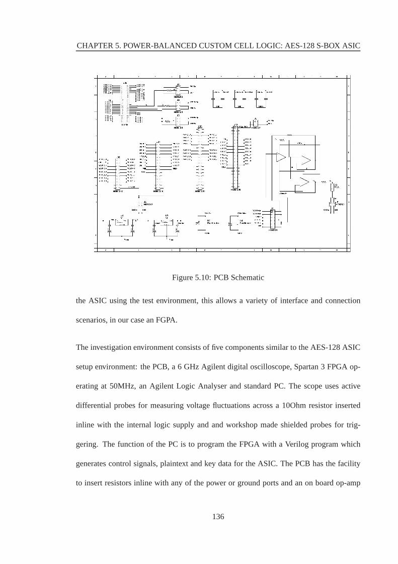
CHAPTER 5. POWER-BALANCED CUSTOM CELL LOGIC: AES-128 S-BOXASIC
Figure 5.10: PCB Schematic
the ASIC using the test environment, this allows a variety ofinterface and connection
scenarios, in our case an FGPA.
The investigation environment consists of five components similar to the AES-128 ASIC
setup environment: the PCB, a 6 GHz Agilent digital oscilloscope, Spartan 3 FPGA op-
erating at 50MHz, an Agilent Logic Analyser and standard PC.The scope uses active
differential probes for measuring voltage fluctuations across a 10Ohm resistor inserted
inline with the internal logic supply and and workshop made shielded probes for trig-
gering. The function of the PC is to program the FPGA with a Verilog program which
generates control signals, plaintext and key data for the ASIC. The PCB has the facility
to insert resistors inline with any of the power or ground ports and an on board op-amp
136

CHAPTER 5. POWER-BALANCED CUSTOM CELL LOGIC: AES-128 S-BOXASIC
Figure 5.11: Logic analyser waveforms
circuit for measuring the current after the experiments on the previous chip. However,
it was found the op-amp circuit did not function particularly efficiently, and the clearest
readings were gained through ground or the internal logic supply; measurements were
taken using the internal logic supply to omit the IO current.
While the ASIC executes, the digital oscilloscope records the power variations (side-
channel information) when triggered by a trigger signal (also used for the clocked S-
box precharge signal). One data acquisition corresponds toa power curve, which the
oscilloscope creates a CSV file of for later processing as required. The logic analyser
reads the output and is used to verify the operation of the cores. For all the experiments
the chip was operated at 12.5 MHz and the oscilloscope set to 2GHz sampling to mimic
reasonable hardware available to attackers.
The first set of experiments conducted verified the setup and function of all the S-box
cores using the logic analyser, example screen dumps are shown in Figure 5.11. The
first subfigure shows the single-rail S-box operation where outputs are produced on each
positive edge of the trigger signal, while the other is takenfrom the clocked precharge
137

CHAPTER 5. POWER-BALANCED CUSTOM CELL LOGIC: AES-128 S-BOXASICF:/sbox/sr_12Mhz_10Ohm_SPA_Z.bmp(a) Single-rail S-box
F:/sbox/dr_12Mhz_10Ohm_SPA_Z.bmp(b) Alternatingspacer S-boxF:/sbox/clked_12Mhz_10Ohm_SPA_Z.bmp
(c) Clockedprecharge S-box
F:/sbox/async_12Mhz_10Ohm_SPA_Z.bmp(d) SelfprechargingS-box
Figure 5.12: Hamming weight experiment
S-box (only the positive rail of the outputs is shown as the other rail is simply inverted)
where the rail switches through precharge to evaluation.
Since this ASIC implements a pure function of AES (SubBytes)rather than being part of a
complex resource sharing architecture simple power analysis experiments were conducted
as follows: averaged waveforms were recorded for a fixed 8-bit key and plaintext causing
the S-box output to compute to 0x00 and then to 0xFF for 500’000 power curves. In other
words, the experiment aims to examine whether there are visual differences when a S-box
is processing data with different hamming weights. Figure 5.12 shows the results, for the
single-rail S-box the 0xFF waveform is higher than the 0x00 waveform and exhibits a
clear difference between processing the two values. Whereas the three differential power-
balanced S-boxes exhibit a repetitive waveform signature from cycle to cycle. These
observations act to illustrate how the single-rail S-box leaks information as the difference
in power consumption is clearly visible compared to the other three designs.
The ideal of power-balancing is, since the hamming weight and distance is constant, to
always have differential traces with a flat profile with no power bias spikes, thus ensuring
138

CHAPTER 5. POWER-BALANCED CUSTOM CELL LOGIC: AES-128 S-BOXASIC
the attacker cannot determine the key. However, the realityis power-balanced designs
still leak information correlated to the key due to the various effects described in Chapter
3; coming down to the fact instantaneous power samples stilldiffer from computation
to computation when processing plaintext data and the secret key. Consequently, with
sufficient sampled power curves, differential traces of power-balanced designs will show
power bias spikes correlated to the key confirming the attackers key hypothesis. With
this in mind, the aim often, with respect to power-balancing, becomes one of minimising
the prominence of the power bias spikes to a level where the key is never revealed over
incorrect key guesses, a phenomenon known as ghost peaks; orsuch that the key cannot
be revealed within its life-time.
Here we have targeted bit zero of each of the S-boxes again, which are each a direct
function of the initial keyK and plaintextP, and constructed the differential means by
creating a set ofN power curve measurements for a set ofN known plaintexts, where the
nthpower curve is computed using thenthplaintext. The set is then split into two subsets
where the targeted bit evaluated to 1 and 0 according to the selection function:
S0 = subBytes(key⊕ plaintext) | D(·) = 0
S1 = subBytes(key⊕ plaintext) | D(·) = 1
The average is then taken of the two subsets and subtracted toobtain the differential trace.
139

CHAPTER 5. POWER-BALANCED CUSTOM CELL LOGIC: AES-128 S-BOXASIC
(a) Single-rail S-box (b) Dual-rail S-box
(c) Clocked precharge S-box (d) Self precharging S-box
Figure 5.13: Differential traces
140

CHAPTER 5. POWER-BALANCED CUSTOM CELL LOGIC: AES-128 S-BOXASIC
Using the described setup, 500’000 power curves were collected for each S-box core
using a fixed 8-bit 0x3F key and varying 8-bit plaintext data,partitioned into two sets
where bit zero computed to 1 and 0 and differential traces constructed, shown in Fig-
ure 5.13. The single-rail core as expected is insecure, and the custom cores demonstrate
an improvement over the alternating spacer S-box. The differential trace of the single-rail
S-box shows significant information leakage and the power bias spike clearly stands out
with an amplitude of 941µA.
The alternating spacer S-box on the other hand substantially reduces the amplitude of the
power-bias spike with a maximum amplitude of 483µA, which is a 48.67% reduction over
the single-rail core and a similar result to the AES-128 ASIC. A power-balanced custom
cell solution still results in power-bias spikes, 256µA and 309µA for the clocked and self-
precharging core respectively. This amounts to a 72.79% and67.16% reduction over the
single rail core and 47.0% and 36.02% over the alternating spacer core. The differences
between the clocked and self-precharging cores security can only be attributed to the
extra cells for self-precharging, which introduce more routing and increase the size of the
layout.
The results show security improvements over single-rail and modest improvements in
power-balancing from using custom cells. The fact that the extracted parasitics for all
the differential S-box cores yielded a less than 8% imbalance between the dual-rail pairs
during layout and the custom gates are as power-balanced as possible, suggests there is
an upper limit in what can be achieved using differential power-balancing and has been
approached here at the cost of large area increases. Therefore the question arises as to
141

CHAPTER 5. POWER-BALANCED CUSTOM CELL LOGIC: AES-128 S-BOXASIC
what else can be applied for power-balancing if informationleakage still occurs at this
upper limit. Furthermore in a commercial environment, eventhough the custom cells are
securer than standard cells, is it worth the design effort and associated area costs.
5.4 Summary
This Chapter has described a custom cell library which implements as much power-
balancing as possible in a UMC 0.18um process; and serves as apower-balanced cell
library available to Europractice institutions. This Chapter has also described a secu-
rity evaluation of a case study AES-128 S-box ASIC. The custom logic S-boxes result
in smaller power bias spikes and information leakage over the alternating spacer S-box,
however leakage still exists; hence the question remains what else can be applied in terms
of power-balancing if everything is already rigorously power-balanced.
142
Chapter 6
Conclusions
Power analysis attacks have to be considered when implementing cryptographic devices.
They are a powerful cryptanalytic tool, and hence, they posea serious threat to the security
of embedded cryptographic devices. They are also a very interdisciplinary subject, and
have led to a wide number of publications and suggestions to counter or address to some
degree power analysis. The different cross sections of industry and academia can be
essentially categorised into two groups. On one hand, poweranalysis attacks can be
viewed as a mathematical problem and measures incorporatedinto the algorithm. On the
other hand, power analysis attacks can be viewed as an engineering problem that can be
solved by decreasing the information leakage. The latter line of thinking leads to different
hardware countermeasures of which differential power-balancing is one.
In general, power-balancing implementations in hardware increase a device’s resistance
to power analysis, however although resistance can be increased, there is no practical
143

CHAPTER 6. CONCLUSIONS
way to achieve perfect security against power analysis attacks through power-balancing.
Each countermeasure has its weakness, for perfect securityin differential logic styles it
would be necessary to balance all cells and wires in a device,however it is not possible in
practice and a best effort approach must be taken. Indeed, a reasonable compromise needs
to be found between the resistance against power analysis attacks and the implementation
costs of the countermeasures.
This thesis has presented two differential balancing methods and their ASIC implementa-
tion. The first a differential power-balanced standard celllogic style, namely alternating
spacer logic, suitable for commercial purposes implemented via the Verimap software.
The crypto-processor implemented a low overhead implementation of AES-128, requir-
ing only 10,372 gates and the dual-rail version 19,510, an increase of 88%. While the
power analysis attack yielded on average a forty fold increase in the number of power
curve measurements required to crack a smartcards secret key. The second a differential
power-balanced custom logic style, implemented in a cell library and tested in a second
case study S-box ASIC. The custom logic S-boxes result in smaller power bias spikes and
information leakage over the alternating spacer S-box, however leakage still exists; hence
the question remains what else can be applied in terms of power-balancing if everything
is already rigorously power-balanced.
Undoubtedly power-balancing and the logic style used can improve a device’s resistance
to power analysis and verified by this research; and options and means to implement it
are required. In summary, unless the lifetime of a secret keyis short and finite, as a
countermeasure alone it is evident it can only reduce a devices susceptibility or increase
144

CHAPTER 6. CONCLUSIONS
moderately the difficulty in cracking the key. The on going and initial future research has
focussed on applying the power balancing techniques developed during the course of this
research to on-chip programmable technology. Smartcards have clearly identifiable sub-
systems which make programmable logic very attractive for implementing cryptographic
algorithms, however akin to normal logic it would be vulnerability to power analysis,
giving substantial scope for future research.
145

Bibliography
[1] ”RESET Roadmap for European Research on Smartcard Technologies”,
http://www.ercim.org/reset/Resetfinal.pdf
[2] http://www.smartcardalliance.org
[3] http://www.smartcard.co.uk
[4] W. Rankl and W. Effing, ”The smartcard Handbook”, John Wiley and Sons, 2nd
edition, ISBN 0471988758.
[5] W. Mao, “Modern Cryptography: Theory and Practice”, Prentice Hall PTR, ISBN
0130669431.
[6] A.J. Menezes, P.C. van Oorschot and S.A. Vanstone, “Handbook of Applied Cryp-
tography”, CRC Press Inc, ISBN 0849385237.
[7] http://standards.ieee.org/getieee802/802.11.html
[8] P. Kocher and B. Jun, “Leak-resistant cryptographic method and apparatus”, US
Patent 6304658, 2001.
146

BIBLIOGRAPHY
[9] J. Jaffe, P. Kocher, B. Jun , ”Balanced Cryptographic Computational Method and
Apparatus for Leak Minimization in Smartcards and other Cryptosystems”, US
Patent 6510518, 2003.
[10] P. Kocher, J. Jaffe and B. Jun, “Differential Power Analysis”, Proceedings of
CRYPTO, pp. 388-397, 1999.
[11] P. Kocher, “Timing Attacks on Implementations of Diffie-Hellman”, Proceedings
of CRYPTO, pp. 104-113, 1996.
[12] J. Dhem et al., “A practical implementation of the timing attack,” UCL Crypto
Group Technical Report Series: CG-1998/1, 1998.
[13] D. Agrawal et al., “The EM Side Channel(s)”, Proceedings of CHES, pp 29-45,
2002.
[14] J. Quisquater and D. Samyde, “Electromagnetic Analysis (EMA): Measures and
Counter-Measures for Smart Cards”, Proceedings of E-smart, pp. 200-210, 2001.
[15] K. Gandolfi, C. Mourtel and F. Oliver, “ElectromagneticAttacks: Concrete re-
sults”, Proceedings of CHES, pp. 158-172, 1999.
[16] R. Anderson and M. Kuhn, “Tamper Resistance –a Cautionary Note”, Proceedings
of the Second USENIX Workshop on Electronic Commerce, pp. 1-11, 1999.
[17] R. Anderson, “Why Cryptosystems Fail,” Proceesings ofthe First ACM Confer-
ence: Computer and Communication Security, pp. 215-227, 1993.
147

BIBLIOGRAPHY
[18] P. Van Oorschot, A. Menezes and S. Vanstone, “Handbook of applied cryptogra-
phy”, CRC Press, ISBN 0849385237.
[19] V. Fisher and M. Drutarovsky, “Two methods of Rijndael implementations in re-
configurable hardware”, Proceedings of CHES, LNCS, pp. 77-84, 2001.
[20] M. McLoone and J. McCanny, “Rijndael FPGA implementations utilising look-
up tables”, Journal of VLSI Signal Processing Systems, Volume 34, Issue 3, pp.
261-275, July 2003.
[21] A. Satoh, S. Morioka, K. Takano and S. Munetoh, “A compact Rijndael hardware
architecture with S-box optimization”, Proceedings of the7th International Con-
ference on the Theory and Application of Cryptology and Information Security:
Advances in Cryptology, pp. 239-254, 2001.
[22] A. Rudra, et al. “Efficient implementation of Rijndael encryption with composite
field arithmetic”, Proceedings of CHES, pp. 171-184, 2001.
[23] X. Zhang and K. Parhi, “High-Speed VLSI Archtectures for the AES Algorithm”,
IEEE transactions on VLSI, Volume 12 , Issue 9, pp. 957 - 967, September 2004.
[24] N. Sklavos and O. Koufopavlou, “Architectures and VLSIimplementations of the
AES proposal Rijndael”, IEEE Transactions on Computers, Volume 51 , Issue 12,
pp. 1454-1459, December 2002.
148
BIBLIOGRAPHY
[25] P. Schaumont and I. Verbauwhede, “Design and Performance Testing of a 2.29-
GB/s Rijndael Processor”, IEEE Journal of Solid-State Circuits, Volume 38, Issue
3, pp. 569 - 572, March 2003.
[26] C. Su et al., “A High Throughout Low Cost AES Processor”,IEEE Communica-
tions Magazine, Dec, 2003.
[27] Stefan Mangard et al., “A Highly Regular and Scalable AES Hardware Architec-
ture”, IEEE transactions on Computers, Volume 52 , Issue 4, pp. 483-491 April
2003.
[28] M. Aigner and E. Oswald, “Power Analysis Tutorial”, SCA-lab, Graz, Austria.
[29] J. Coron et al., “Statisitics and Secret Leakage”, ACM Transactions on Embedded
Computing Systems, Volume 3, Issue 3, pp. 492-508, August 2004.
[30] J. Wolkerstorfer, E. Oswald, and M. Lamberger, "An ASICimplementation of the
AES S-Boxes", Proceedings of the The Cryptographer’s Trackat the RSA Confer-
ence on Topics in Cryptology, pp. 67-78, 2002.
[31] J. Daemen and V. Rijmen, “The Design of Rijndael”, Springer-Verlag, ISBN
3540425802.
[32] D. Sokolov, J. Murphy, A. Bystrov, A. Yakovlev, “Designand Analysis of Dual-rail
Circuits for Security Applications”, IEEE Transactions onComputers, Volume 54,
Issue 4, pp. 449 - 460, April 2005.
149

BIBLIOGRAPHY
[33] T. Popp and S. Mangard, “Masked Dual-Rail Pre-charge Logic: DPA-Resistance
Without Routing Constraints”, Proceedings of CHES, pp. 172-186, 2005.
[34] S. Moore et al., “Improving Smart card Security using Self-timed Circuits”, Pro-
ceedings of ASYNC, pp. 211-218, 2002.
[35] K. Tiri et al., "Prototype IC with WDDL and DifferentialRouting - DPA Resistance
Assessment", Proceedings of CHES, pp. 354-365, 2005.
[36] P. Wayner, “Code Breaker Cracks Smart Cards? “, New YorkTimes, page D1, 22
June 1998.
[37] L. Goubin and J. Patarin, “DES and Differential Power Analysis - The Duplication
Method”, Proceedings of CHES, pp. 158 - 172, 1999.
[38] T. S. Messerges, E. Dabbish, and R. Sloan, “Investigations of Power Analysis At-
tacks on Smartcards”, In USENIX Workshop on Smartcard Technology, pp. 151-
161, 1999.
[39] T. S. Messerges, “Using Second-Order Power Analysis toAttack DPA Resistant
Software”, Proceedings of CHES, pp. 27-78, 2000.
[40] M. L. Akkar and L. Goubin, “A Generic Protection againstHigh-Order Differential
Power Analysis”, Proceedings of FSE, pp. 192-205, 2003.
[41] J. Daemen, M. Peeters, and G. Van Assche, “Bitslice Ciphers and Power Analysis
Attacks”, Proceedings of FSE, pp. 134-149, 2000.
150

BIBLIOGRAPHY
[42] E. Biham and A. Shamir, “Power Analysis of the Key Scheduling of the
AES-128-128 Candidates”, In Second Advanced Encryption Standard Candidate
Conference, http://csrc.nist.gov/encryption/AES-128-128/round1/conf2/AES-128-
1282conf.htm, 1999.
[43] C. Clavier, J. S. Coron, and N. Dabbous, “Differential Power Analysis in Presence
of Hardware Countermeasures”, Proceedings of CHES, pp. 252-263, 2000.
[44] L. Goubin and J. Patarin, “DES and differential power analysis”, Proceedings of
CHES, pp. 158-172, 1999.
[45] S. Chari, C. Jutla, J. Rao and P. Rohatgi, “Towards SoundApproaches to Counter-
act Power-analysis Attacks”, Proceedings of CRYPTO, pp 398-412, 1999.
[46] C. Clavier, J.S. Coron and N. Dabbous, “Differential Power Analysis in the pres-
ence of Hardware Countermeasures”, Proceedings of CHES, pp. 252-263, 2000.
[47] L. Goubin, “A Sound Method for Switching between Boolean and Arithmetic
Masking”, Proceedings of CHES, pp. 3-15, 2001.
[48] E. Trichina, D. Seta and L. Germani, “Simplified Adaptive Multiplicative amsking
for AES-128”, Proceedings of CHES, pp. 187-197, 2002.
[49] C. Walter, “Longer keys may facilitate side channel attacks”, Proceedings of SAC,
pp. 42-57, 2004.
[50] S. Mangard, “Hardware Countermeasures against DPA? A Statistical Analysis of
their Effectiveness”, Proceedings of RSA, pp. 222-235, 2005.
151
BIBLIOGRAPHY
[51] S. Chari, C. Jutla, J. Rao and P. Rohatgi, “A Cautionary Note Regarding
Evaluation of AES-128 Candidates on Smart-Cards”, In Second Advanced En-
cryption Standard Candidate Conference, http://csrc.nist.gov/encryption/AES-128-
128/round1/conf2/AES-128-1282conf.htm, 1999.
[52] J. Daemen and V. Rijmen, “Resistance Against Implementation Attacks: A
Comparative Study of the AES-128 Proposals”, In Second Advanced Encryp-
tion Standard Candidate Conference, http://csrc.nist.gov/encryption/AES-128-
128/round1/conf2/AES-128-1282conf.htm, 1999.
[53] T. Messerges, “Securing the AES-128-128 Finalists Against Power Analysis At-
tacks”, Proceedings of FSE, pp. 150-158, 2000.
[54] J. Coron and L. Goubin, “On Boolean and Arithmetic Masking against Differential
Power Analysis”, Proceedings of CHES, pages 231-239, 2000.
[55] A. Shamir, “Protecting Smart Cards from Passive Power Analysis with Detached
Power Supplies”, Proceedings of CHES, pp 71-77, 2000.
[56] T. Messerges, “Power Analysis Attack Countermeasuresand Their Weaknesses”
Proceedings of Communications, Electromagnetics, Propagation, and Signal Pro-
cessing Workshop, 2000.
[57] N. Weste and K. Eshraghian, “Principles of CMOS VLSI Design - A Systems
Perspective”, Addison-Wesley, 2nd edition, ISBN 0201533766, 1993.
152

BIBLIOGRAPHY
[58] T. Caddy, ”Physical Security 101”, Proceedings of Physical Security Testing Work-
shop, 2005.
[59] S. Kladko, ”SPA and DPA: Possible Testing Solutions andAssociated Costs“, Pro-
ceedings of Physical Security Testing Workshop, 2005.
[60] P. Kocher, ”Design and Validation Strategies for Obtaining Assurance in Counter-
measures to Power Analysis and Related Attacks”, Proceedings of Physical Secu-
rity Testing Workshop, 2005.
[61] K. Kulokowski, M. Karpovski and A. Taubin, “Power Attacks on Secure Hardware
Based on Early Propagation of Data”, Proceedings of IOLTS, pp. 131-138, 2006.
[62] K. Kulikowski, M. Su, A. Taubin, M. Karpovsky, “Delay Insensitive Encoding and
Power Analysis: A Balancing Act”, Proceedings of ASYNC, pp.116-125, 2005.
[63] C. Brej, “Early Output Logic and Anti-Tokens”, PhD thesis, School of Computer
Science, University of Manchester, 2006.
[64] K. Tiri and I. Verbauwhede, “Place and Route for Secure Standard Cell Design”,
Proceedings of CARDIS, 2004.
[65] S. Guiley, P. Hoogvorst, Y. Mathieu and R. Pacalet, “TheBackend Duplication
Method”, Proceedings of CHES, pp. 383-397, 2005.
[66] M. Aigner and S. Mangard et al., “Side-channel AnalysisResistant Design Flow”,
Proceedings of ISCAS, pp. 4-9, 2006.
153

BIBLIOGRAPHY
[67] G. Bouesse, M. Renaudin et al., “DPA on quasi delay insensitive asynchronous
circuits: formalization and improvement”, Proceedings ofDAT, pp. 424-429, 2005.
[68] Z. Yu, ”An Investigation into the Security of Self-timed Circuits”, PhD Thesis,
School of Computer Science, University of Manchester, 2004.
[69] S. Guilley et al., “CMOS Structures Suitable for Secured Hardware”, Proceedings
of DATE, pp. 1414-1415, 2004.
[70] J. Sparso and J. Staunstrup, “Delay-insensitive multi-ring structures”, The VLSI
Journal of Integration, Volume 15, Issue 3, pp. 313-340, October 1993.
[71] Bouesse, G.F. Renaudin, M. Witon and A. Germain, “A clock-less low-voltage
AES crypto-processor” Proceedings of ESSCIRC, pp. 403-406, 2005.
[72] K. Tiri, M. Akmal, and I. Verbauwhede, "A Dynamic and Differential CMOS Logic
with Signal Independent Power Consumption to Withstand Differential Power
Analysis on Smart Cards", Proceedings of ESSCIRC, pp. 403-406, 2002.
[73] B. Nikolic et al, “Improved Sense-Amplifier-Based FlipFlop: Design and Mea-
surements,” IEEE Journal of Solid-State Circuits, Volume 35, pp. 876-883, June
2000.
[74] F. Mace, et al., “A Dynamic Current Mode Logic to Counteract Power Analysis
Attacks”, Proceedings of DCIS, pp. 550-560, 2004.
[75] D. Sokolov, J. Murphy, A. Bystrov and A. Yakovlev, "Improving the security of
dual-rail circuits", Proceedings of CHES, pp. 282-297, 2004.
154

BIBLIOGRAPHY
[76] J. Murphy and A. Yakovlev, "An Alternating Spacer AES Crypto-processor", Pro-
ceedings of ESSCIRC, pp. 126-129, 2006.
[77] J. Murphy and A. Yakovlev, "Power-balanced Asynchronous Logic", Proceedings
of ECCTD, pp. 213-216, 2005.
[78] A. Kondratyev and K. Lwin, “Design of Asynchronous Circuits Using Syn-
chronous CAD Tools”, IEEE Design and Test archive, Volume 19, Issue 4, pp
107-117, July 2002.
[79] J. Murphy and A. Yakovlev, "Power-balanced Self Checking Circuits for Crypto-
graphic Chips", Proceedings of IOLTS, pp. 157 - 162, 2005.
[80] http://www.theseus.com
[81] C. Paar, “Efficient VLSI Architectures for Bit ParallelComputation in Galois
Fields”, PhD thesis, University GH Essen, VDI Verlag, 1994.
[82] C. C. Lu and S. Y. Tseng, “Integrated design of AES Encrypter and Decrypter”,
Proceedings of Application Specific Systems, Architectures and Processors, pp.
227-285, 2002.
[83] H. Huo and I. Verbauwhede, “Architectural optimisation for a 1.82 Gbit/sec VLSI
implementation of the Rijndael algorithm”, Proceedings ofCHES, pp. 51-64, 2001.
[84] N. Kim, T. Mudge and R. Brown, “A 2.3Gb/s fully integrated and synthesizable
AES Rijndael core”, Proceedings of IEEE Custom Integrated Circuits, pp. 193-
196, 2003.
155

BIBLIOGRAPHY
[85] C. Su et al., “A high-throughput low-cost AES processor”, IEEE Communication
Magazine, Issue 41, pp. 86-91, 2003.
[86] F. K Gurkaynak et al., “A 2Gb/s balanced AES crypto-chipimplementation”, Pro-
ceedings of 14th ACM Great Lakes Symm on VLSI, 2004.
[87] T. Ichikawa et al., “Hardware evaluation of the AES finalists”, Proceedings of 3rd
AES Candidate Conference, 2000.
[88] D. Sokolov, “Automated Synthesis of Asynchronous Circuits Using Direct Map-
ping for Control and Datapath”, PhD Thesis, University of Newcastle upon Tyne,
2006.
[89] http://csrc.nist.gov/publications/fips/fips197/fips-197.pdf, “AES Specification”,
2001.
[90] “Data Encryption Standard”, National Bureau of Standards, U.S. Department of
Commerce, Washington D.C., January 1977.
[91] E. Biham and A. Shamir, “Differential Cryptanalysis ofDES-like Cryptosystems”
Proceedings of CRYPTO, pp. 221, 1990.
[92] D. Boneh, R. DeMillo and R. Lipton, “On the Importance ofChecking Crypto-
graphic Protocols for Faults”, Proceedings of EUROCRYPT, pp. 37-51, 1997.
[93] O. Standaert, et al., ”An overview of power analysis attacks against field pro-
grammable gate arrays”, Proceedings of the IEEE, Feb 2006.
156

BIBLIOGRAPHY
[94] J. Greenbaum, “Reconfigurable loic in SOC systems”, in Proc. Custom Intregrated
Circuits Conf., May 2002, pp. 5-8.
[95] S. J. E. Wilton and R. Saleh, “Programmable logic IP cores in SoC design: Oppor-
tunities and challenges”, in Proc. Custom Integrated Circuits Conf., May 2001, pp.
63-66.
[96] ”VariCore Embedded Programmable Gate Array Core (EPGA) 0.18um Family”,
Actel Corp., Mountain View, CA, Dec 2001.
[97] M2000 FLEXEOStm Configurable IP core, http://www.m2000.fr M2000 Inc.
[98] eASIC 0.13um Core, http://www.easic.com eASIC.
[99] M. Borgatti, F. Lertora, B. Foret and L. Cali, “A reconfigurable system featuring
dynamically extensible embedded microprocessor FPGA and customisable I/O”,
IEEE Journal Solid-State Circuits, vol. 38, no. 3, pp. 521-529, Mar, 2003.
[100] T. Vaida, “PLC advanced technology demonstrator testchip”, in Proc. Custom
Integrated Circuits Conf., May 2001, pp. 67-70.
[101] P. S. Zuchowski et al., “A hybrid ASIC and FPGA architecture,” in Proc, Int. Conf.
Computer-Aided Design, Nov 2002, pp. 184-194.
[102] T. Vaida, “Reprogrammable processing capabilities of embedded FPGA blocks”,
in Proc. IEEE Int. ASIC/SOC Conf., Sep 2001, pp. 180-184.
[103] F. Lien et al., “A hardware/software solution for embedbbable FPGA”, in Proc.
Custom Integrated Circuits Conf., May 2001, pp. 71-74.
157

BIBLIOGRAPHY
[104] S. B. Ors, E. Oswald and B. Preneel, “Power-analysis attacks on an FPGA—First
experimental results,” CHES 2003, pp. 35-50.
[105] S. B. Ors, F. Gurkaynak, E. Oswald and B. Preneel, “Power-analysis attack on an
ASIC AES implementation,” ITCC 2004.
[106] F. X. Standaert, S. B. Ors and B. Preneel, “Power analysis of an FPGA implemen-
tation of Rijndael: is pipelining a DPA countermeasure?,” CHES 2004, pp. 30-44.
[107] F. X. Standaert, S. B. Ors, J. J. Quisquater and B. Preneel, “Power analysis attacks
against FPGA implementations of DES,” FPLA 2004, pp. 84-94.
[108] P. Buysschaert, E. De Mulder, S. B. Ors, P. Delmotte, B.Preneel, G. Vandenbosch
and I. Verbauwhede, “Electromagnetic analysis attack on anFPGA implementation
of an elliptic curve cryptosystem,” EUROCON 2005.
[109] M. Hutton, J. Rose, J. Grossman and D. Corneil, “Characterisation and param-
eterised generation of synthetic combinational benchmarkcircuits,” IEEE Trans.
Computer Aided Design, vol. 17, no. 10, pp. 985-996, Oct 1998.
158