srinivasa rao pathapati - diva portalliu.diva-portal.org/smash/get/diva2:731090/fulltext02.pdf ·...
TRANSCRIPT
Institutionen för systemteknik Department of Electrical Engineering
Examensarbete
All-Digital ADC Design in 65 nm CMOS Technology
Examensarbete utfört i Elektroniksystem vid Tekniska högskolan vid Linköpings universitet av
Srinivasa Rao Pathapati
LiTH-ISY-EX--14/4758--SE
Linköping 2014
Department of Electrical Engineering Linköpings tekniska högskolaLinköpings universitet Linköpings universitetSE-581 83 Linköping, Sweden 581 83 Linköping
TEKNISKA HÖGSKOLAN
All-Digital ADC Design in 65 nm CMOS Technology
Examensarbete utfört i Elektroniksystem vid Tekniska högskolan vid Linköpings universitet av
Srinivasa Rao Pathapati
LiTH-ISY-EX--14/4758--SE
Handledare: Vishnu Unnikrishnan ISY, Linköpings universitet
Examinator: Dr. Mark Vesterbacka ISY, Linköpings universitet
Linköping, 27 May 2014
i

Presentation Date
27-05-2014
Publishing Date (Electronic version)
Department and Division
Institutionen för systemteknik Avdelningen för elektroniksystem
Department of Electrical Engineering Division of Electronics Systems
Språk Svenska
. English
Typ av publikation Licentiatavhandling . Examensarbete C-uppsats D-uppsats Rapport Annat (ange nedan)
ISBN (licentiatavhandling)
ISRNLiTH-ISY-EX--14/4758--SE
Serietitel (licentiatavhandling)
Serienummer/ISSN (licentiatavhandling)
URL, Electronic Versionhttp://www.ep.liu.se
Publication TitleTitle All-Digital ADC Design in 65 nm CMOS Technology
Author Srinivasa Rao Pathapati Abstract
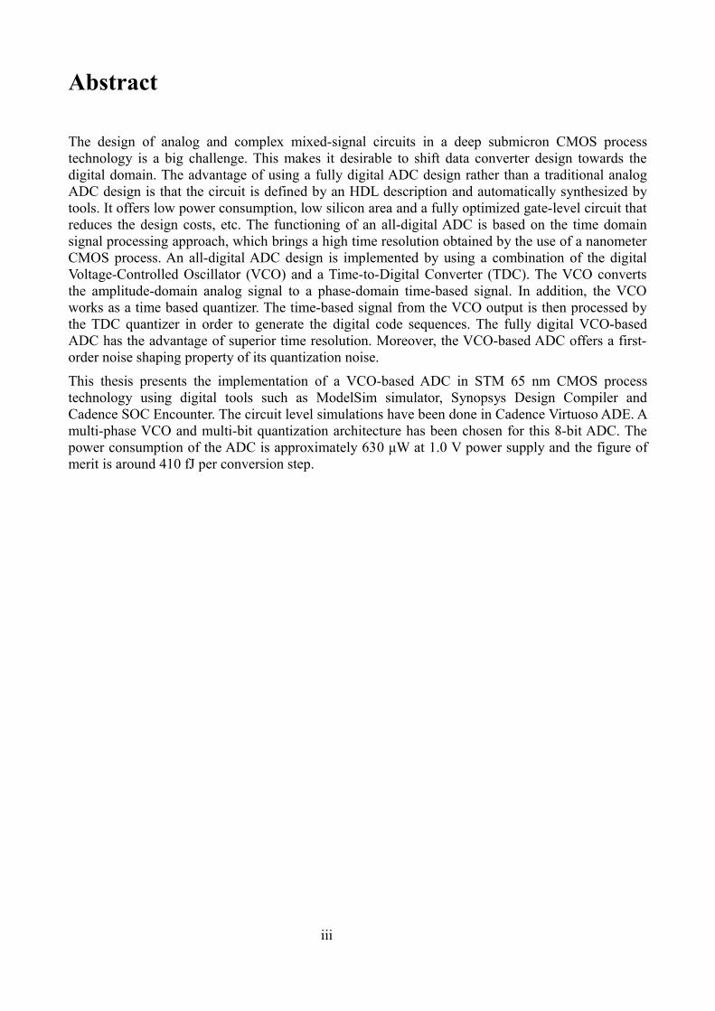
The design of analog and complex mixed-signal circuits in a deep submicron CMOS processtechnology is a big challenge. This makes it desirable to shift data converter design towards thedigital domain. The advantage of using a fully digital ADC design rather than a traditional analogADC design is that the circuit is defined by an HDL description and automatically synthesized bytools. It offers low power consumption, low silicon area and a fully optimized gate-level circuit thatreduces the design costs, etc. The functioning of an all-digital ADC is based on the time domainsignal processing approach, which brings a high time resolution obtained by the use of a nanometerCMOS process. An all-digital ADC design is implemented by using a combination of the digitalVoltage-Controlled Oscillator (VCO) and a Time-to-Digital Converter (TDC). The VCO convertsthe amplitude-domain analog signal to a phase-domain time-based signal. In addition, the VCOworks as a time based quantizer. The time-based signal from the VCO output is then processed bythe TDC quantizer in order to generate the digital code sequences. The fully digital VCO-basedADC has the advantage of superior time resolution. Moreover, the VCO-based ADC offers a first-order noise shaping property of its quantization noise.
This thesis presents the implementation of a VCO-based ADC in STM 65 nm CMOS processtechnology using digital tools such as ModelSim simulator, Synopsys Design Compiler andCadence SOC Encounter. The circuit level simulations have been done in Cadence Virtuoso ADE. Amulti-phase VCO and multi-bit quantization architecture has been chosen for this 8-bit ADC. Thepower consumption of the ADC is approximately 630 μW at 1.0 V power supply and the figure ofmerit is around 410 fJ per conversion step.
KeywordsDigital ADC, TDC, VCO-based ADC, VCO-based quantizer.
ii
Abstract
The design of analog and complex mixed-signal circuits in a deep submicron CMOS processtechnology is a big challenge. This makes it desirable to shift data converter design towards thedigital domain. The advantage of using a fully digital ADC design rather than a traditional analogADC design is that the circuit is defined by an HDL description and automatically synthesized bytools. It offers low power consumption, low silicon area and a fully optimized gate-level circuit thatreduces the design costs, etc. The functioning of an all-digital ADC is based on the time domainsignal processing approach, which brings a high time resolution obtained by the use of a nanometerCMOS process. An all-digital ADC design is implemented by using a combination of the digitalVoltage-Controlled Oscillator (VCO) and a Time-to-Digital Converter (TDC). The VCO convertsthe amplitude-domain analog signal to a phase-domain time-based signal. In addition, the VCOworks as a time based quantizer. The time-based signal from the VCO output is then processed bythe TDC quantizer in order to generate the digital code sequences. The fully digital VCO-basedADC has the advantage of superior time resolution. Moreover, the VCO-based ADC offers a first-order noise shaping property of its quantization noise.
This thesis presents the implementation of a VCO-based ADC in STM 65 nm CMOS processtechnology using digital tools such as ModelSim simulator, Synopsys Design Compiler andCadence SOC Encounter. The circuit level simulations have been done in Cadence Virtuoso ADE. Amulti-phase VCO and multi-bit quantization architecture has been chosen for this 8-bit ADC. Thepower consumption of the ADC is approximately 630 μW at 1.0 V power supply and the figure ofmerit is around 410 fJ per conversion step.
iii

Acknowledgment
First, I would like to sincerely thank my supervisor Mr. Vishnu Unnikrishnan for the timeinvestment, who greatly helped throughout the thesis work. His guidance helped me to understandthe theoretical concepts and design issues.
Special thanks should be extended to examiner Dr. Mark Vesterbacka for giving the opportunity towrite my master thesis, his assistance and generous support throughout.
iv

Table of Contents1 Introduction.......................................................................................................................................1
1.1 Bottleneck of analog ADC design.............................................................................................11.2 The advantage of fully digital ADC design ..............................................................................21.3 Purpose.......................................................................................................................................31.4 Thesis organization....................................................................................................................4
2 General characteristics of ADCs........................................................................................................5 2.1 Static parameters........................................................................................................................6 2.2 Frequency-domain dynamic parameters..................................................................................10 2.3 Oversampling and noise shaping property...............................................................................133 VCO-based ADC.............................................................................................................................15
3.1 Introduction to VCO-based ADCs...........................................................................................153.2 Architectures............................................................................................................................16
3.2.1 Single-phase VCO-based ADC........................................................................................163.2.2 Multi-phase VCO-based ADC.........................................................................................17
3.3 Voltage-controlled oscillator....................................................................................................193.4 Basic working principles.........................................................................................................20
3.4.1 First order noise-shaping..................................................................................................223.4.2 Quantizer resolution.........................................................................................................23
3.5 Non-ideal effects of the VCO-based ADC...............................................................................233.5.1 VCO nonlinearity.............................................................................................................243.5.2 VCO phase noise..............................................................................................................243.5.3 Mismatch of VCO delay cells..........................................................................................253.5.4 Flip-flop metastability......................................................................................................253.5.5 Sampling clock jitter........................................................................................................27
4 Design..............................................................................................................................................294.1 The architecture.......................................................................................................................294.2 Ring-oscillator as a VCO.........................................................................................................304.3 Counter design.........................................................................................................................314.4 Differentiator............................................................................................................................314.5 Adder array..............................................................................................................................32
5 Simulation results............................................................................................................................335.1 Test bench setup.......................................................................................................................33
5.1.1 FFT testing.......................................................................................................................345.2 Flip-flop metastability..............................................................................................................375.3 Power consumption..................................................................................................................39
5.3.1 Figure-of-merit.................................................................................................................406 Design flow.....................................................................................................................................41
6.1 ADC design flow.....................................................................................................................416.2 Synthesis flow..........................................................................................................................416.3 HDL implementation...............................................................................................................436.4 Design compiler initialization..................................................................................................43
6.4.1 Libraries specification......................................................................................................446.4.2 Analyze and elaborate design...........................................................................................456.4.3 Design constraints............................................................................................................466.4.4 Design environment.........................................................................................................476.4.5 Optimize design...............................................................................................................496.4.6 Database...........................................................................................................................49
6.5 Place & route for VCO-based ADC.........................................................................................50
v

6.5.1 Design import...................................................................................................................516.5.2 Floorplan..........................................................................................................................516.5.3 Power planning................................................................................................................526.5.4 Substrate bias planning....................................................................................................536.5.5 Power grid........................................................................................................................546.5.6 Placing standard cells.......................................................................................................546.5.7 Optimization.....................................................................................................................546.5.8 Clock tree synthesis (optional).........................................................................................556.5.9 Design routing..................................................................................................................566.5.10 Gaps filling.....................................................................................................................566.5.11 Design checks.................................................................................................................576.5.12 Export files.....................................................................................................................57
6.6 Design import in Cadence Virtuoso.........................................................................................586.6.1 Layout area.......................................................................................................................586.6.2 Design verification in Calibre..........................................................................................59
7 Conclusion ......................................................................................................................................617.1 Future work .............................................................................................................................61
Appendix...........................................................................................................................................63
References........................................................................................................................................68
Bibliography.....................................................................................................................................69
vi

List of FiguresFigure 1.1. Organization of an all-digital ADC....................................................................................3Figure 2.1. An 8-level ideal ADC coding scheme................................................................................5Figure 2.2. Ideal vs. non-ideal 3-bit ADC transfer function characteristics.........................................6Figure 2.3. Measuring DNL.................................................................................................................7Figure 2.4. Measuring INL...................................................................................................................8Figure 2.5. Quantization error voltage for 3-bit ideal ADC.................................................................9Figure 2.6. Power spectrum density plot for an ADC.........................................................................11Figure 2.7. Two-tone IMD spectrum..................................................................................................13Figure 2.8. Spectral distribution of quantization noise in Nyquist-rate ADCs...................................14Figure 2.9. Spectral distribution of quantization noise in oversampling ADCs.................................14Figure 3.1. Basic architecture of a VCO-based ADC.........................................................................15Figure 3.2. Single-phase with multi-bit quantization architecture.....................................................16Figure 3.3. Operation of single-phase VCO-based quantizer.............................................................17Figure 3.4. Multi-phase VCO-based ADC architecture.....................................................................17Figure 3.5. Single-bit quantization architecture.................................................................................18Figure 3.6. Multi-bit quantization architecture...................................................................................18Figure 3.7. Ideal vs. non-ideal VCO tuning curve..............................................................................19Figure 3.8. Working principle of an ideal VCO-based ADC..............................................................20Figure 3.9. First-order noise-shaping property of the VCO-based ADC............................................22Figure 3.10. Setup and hold-time definitions.....................................................................................26Figure 3.11. The metastable window definition.................................................................................26Figure 3.12. Effect of flip-flop metastability......................................................................................27Figure 3.13. Timing diagram of sampling clocks with and without jitter..........................................28Figure 4.1. Implemented VCO-based ADC architecture....................................................................29Figure 4.2. VCO tuning characteristics..............................................................................................30Figure 4.3. The differentiator circuit..................................................................................................31Figure 4.4. The cascaded adders structure..........................................................................................32Figure 5.1. Test bench for VCO-based ADC simulations..................................................................34Figure 5.2. Simulated VCO-based ADC digital output in time domain.............................................35Figure 5.3. Simulated VCO-based ADC PSD plot.............................................................................36Figure 5.4. VCO-based ADC PSD plot with noise-shaping property................................................37Figure 5.5. Flip-flop metastability in the implemented VCO-based ADC.........................................38Figure 5.6. Error in the differentiator output due to flip-flop metastability.......................................38Figure 5.7. Current consumption plots for VCO-based ADC............................................................39Figure 6.1. Flow-chart for VCO-based ADC design flow..................................................................42Figure 6.2. Technology libraries specification in DC GUI.................................................................44Figure 6.3. HDL files setup................................................................................................................45Figure 6.4. Design constraints specification for VCO........................................................................46Figure 6.5. Clock signal specification................................................................................................47Figure 6.6. Selecting wire load...........................................................................................................48Figure 6.7. Setting operating conditions.............................................................................................48Figure 6.8. SOC Encounter physical design flow chart.....................................................................50Figure 6.9. Floorplan specification of the ADC.................................................................................52Figure 6.10. Power planning around the core.....................................................................................53Figure 6.11. Insertion of body-bias cells at the core row end points..................................................54Figure 6.12. Pre-CTS optimization for VCO-based ADC..................................................................55Figure 6.13. Clock tree display for cell placement in ADC design....................................................56Figure 6.14. Specification of the core filler cells in the ADC............................................................57
vii

Figure 6.15. gds file streaming...........................................................................................................58Figure 6.16. Layout of the implemented TDC...................................................................................59Figure 6.17. Calibre LVS standard cells black box specification.......................................................60
List of TablesTable 1.1. The tools used for implementing the all-digital ADC..........................................................4Table 5.2. VCO-based ADC performance summary .........................................................................36Table 5.1. ADC power consumption..................................................................................................39Table 6.1. Synthesis flow summary ...................................................................................................43Table 6.2. Summary of major optimization constraints......................................................................46Table 6.2. Database to import in Encounter.......................................................................................52Table 6.3. Technology files database to be imported in Encounter....................................................52Table 6.5. Pre-CTS optimized summary for TDC in the VCO-based ADC ......................................55
viii
Abbreviations
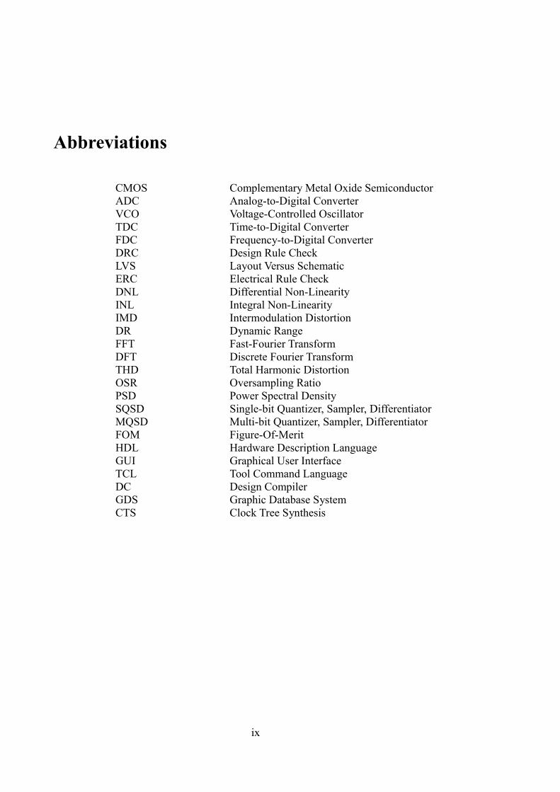
CMOS ADC VCO TDC FDC DRC LVSERCDNLINLIMDDRFFT DFT THD OSR PSD SQSD MQSD FOM HDLGUI TCLDC GDSCTS
Complementary Metal Oxide SemiconductorAnalog-to-Digital ConverterVoltage-Controlled Oscillator Time-to-Digital ConverterFrequency-to-Digital ConverterDesign Rule CheckLayout Versus SchematicElectrical Rule CheckDifferential Non-Linearity Integral Non-Linearity Intermodulation Distortion Dynamic Range Fast-Fourier Transform Discrete Fourier TransformTotal Harmonic DistortionOversampling Ratio Power Spectral Density Single-bit Quantizer, Sampler, DifferentiatorMulti-bit Quantizer, Sampler, DifferentiatorFigure-Of-Merit Hardware Description Language Graphical User InterfaceTool Command LanguageDesign CompilerGraphic Database SystemClock Tree Synthesis
ix

x

1 Introduction
1 Introduction
Obtaining compact design, low power consumption, and low design cost is a difficult challenge inelectronic systems design. Supply voltage and device dimensions scaling are effects of the scalingin CMOS process technology according to Moore's law. Data converter design is essential in a widerange of mixed-signal processing applications. High speed signal operation and output dataaccuracy are the key necessities of the signal processing systems. For example, the RF transceiveruses such a mixed-signal processing system. The analog domain (continuous time and amplitude) isstill a high priority for information carrying the electrical signals. An Analog-to-Digital Converter(ADC) converts an analog signal into a digital signal. The digitized signal is a set of discrete valuesthat is processed by the digital processor. Most of the cases in RF transceivers, the analog, RF,digital logic circuits and digital memory blocks are integrated on the same silicon die. Conventionaldata converters are often built with passive elements or analog circuits. For example, usual analogADCs are pipeline ADC, flash ADC, time-interleaved ADC, and sigma-delta ADC. Most of theanalog ADCs traditionally contain sample and hold circuits, Digital-to-Analog Converter (DAC)functionality, operational amplifiers, and external or internal reference voltage circuits. Hence,analog and mixed-signal circuit design requires great care to minimize the signal crosstalk andcoupling. The power-efficiency and silicon area-efficiency of CMOS technology scaling areimportant aspects in the prospective ADC design. In addition, the use of deep submicron CMOSprocess technology tends to increase the challenges for the ADC design.
The implementation of the data converters using fully digital hardware is more convenient than itsequivalent analog design. These facts favors the development of the fully digital ADC over theanalog ADC in mixed-signal processing systems. Moreover, the digital circuits are less sensitivethan analog circuits. The major influential factors in analog and digital design of an ADC circuit areoutlined in the below sections.
1.1 Bottleneck of analog ADC design
In almost all cases, the analog circuits are implemented by cascading the analog devices and passiveelements. An ADC design in analog EDA (Electronic-Design-Automation) tools is implemented bya fully handcrafted and manual effort. Hence, the design process increases the resource costs onanalog circuit design and the implementation takes a long time and is error-prone. It is difficult toreuse a previous analog circuit since it has been defined using device dimensions and amathematical model. In addition, there is always a trade-off between the supply voltage, gain,precision, and power dissipation in the analog circuit design. In this section, a few aspects arediscussed to illustrate the general difficulties of an analog ADC design in the presence of CMOSprocess technology scaling [1].
(i) The influence of reducing supply voltage: The tolerance of the reduction in supplyvoltage and doping levels becomes more influential on the analog circuit performance in adeep submicron CMOS process. The traditional analog ADC (e.g., pipeline ADC)resolution can be deduced from the supply voltages or current levels. The reduced input
1

1 Introduction
supply voltage due to the technology scaling also reduces the input signal dynamic range.Thus, it limits the signal processing speed of the analog circuits. In addition, the analogcircuits require more power for the output signal accuracy.
(ii) Transconductance: The short channel length of a transistor has brought down the valueof the transconductance in the velocity saturation mode. The transconductance value is afunction of the bias current (output current). Decrease in supply voltage and velocitysaturation causes the value of the transconductance to decrease. Low transconductance ofthe devices degrades the linear behavior and driving capability of the circuits.
(iii) Output resistance: The device dimensions become smaller by decreasing the scalingfactor for all geometry parameters of the circuit in the CMOS technology. The transistoroutput resistance is lowered with its short channel length. Hence, the intrinsic gain of thedevice goes down with reduced output resistance together with the transconductance.
(iv) Mixed-signal integrity: The ultra-deep submicron process would cause substratecoupling, power supply line coupling, and electromagnetic interference by sharing theanalog and digital circuits on the same die. The high speed digital switching can bedirectly coupled to the RF and analog circuitry in case of mixed-signal IC design. Thiscoupled noise and signal interactions lower the signal swing and circuit performance.
1.2 The advantage of fully digital ADC design
The attractive feature of an ADC design is programmability in the hardware description language(HDL). An ADC design in digital EDA tools has been implemented using a HDL description. Thedesigned circuit offers full automation at various circuit levels. Further, it drastically reduces thedesign cost when compared to the traditional analog ADC and brings down the design time. Someadvantages of an ADC design fully digital in nature are listed below.
(i) A fully digital ADC design benefits from the CMOS technology scaling. Smallergeometrical dimensions lower the parasitics on the digital circuits. The effect of smallparasitic elements in a circuit can reduce the transition time of signals. In addition, thereduced parasitics lead to improvement of the signal processing speed as well as circuitswitching time.
(ii) Reducing the device sizes results in low power consumption and greatly reduces thesilicon area.
In general, the digital signal processing systems are more immune to noise. On the other hand, it isessential to limit the external noise sources as well as the internal noise in the analog circuits. Theanalog circuits are always placed away from the digital block on the same Integrated Circuit (IC)design to mitigate the interference. This will result in that the analog and digital circuit integrationon the same chip increases the chip area, power consumption, and design cost. The idea of using theanalog functions in the digital domain is inevitable in mixed-signal processing applications.
2
1 Introduction
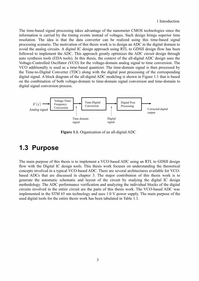
The time-based signal processing takes advantage of the nanometer CMOS technologies since theinformation is carried by the timing events instead of voltages. Such design brings superior timeresolution. The idea is that the data converter can be realized using this time-based signalprocessing scenario. The motivation of this thesis work is to design an ADC in the digital domain toavoid the analog circuits. A digital IC design approach using RTL to GDSII design flow has beenfollowed to implement the ADC. This approach greatly optimizes the ADC circuit design throughauto synthesis tools (EDA tools). In this thesis, the context of the all-digital ADC design uses theVoltage-Controlled Oscillator (VCO) for the voltage-domain analog signal to time conversion. TheVCO additionally is used as a time-based quantizer. The time-domain signal is then processed bythe Time-to-Digital Converter (TDC) along with the digital post processing of the correspondingdigital signal. A block diagram of the all-digital ADC modeling is shown in Figure 1.1 that is basedon the combination of both voltage-domain to time-domain signal conversion and time-domain todigital signal conversion process.
1.3 Purpose
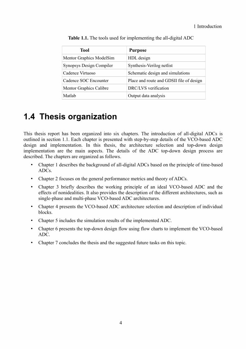
The main purpose of this thesis is to implement a VCO-based ADC using an RTL to GDSII designflow with the Digital IC design tools. This thesis work focuses on understanding the theoreticalconcepts involved in a typical VCO-based ADC. There are several architectures available for VCO-based ADCs that are discussed in chapter 3. The major contribution of this thesis work is togenerate the automatic schematic and layout of the circuit by studying the digital IC designmethodology. The ADC performance verification and analyzing the individual blocks of the digitalcircuits involved in the entire circuit are the parts of this thesis work. The VCO-based ADC wasimplemented in the STM 65 nm technology and uses 1.0 V power supply. The main purpose of theused digital tools for the entire thesis work has been tabulated in Table 1.1.
3
Figure 1.1. Organization of an all-digital ADC
Voltage-Time/FrequencyConversion
Digital Post Processing
Time-Digital Conversion
Corrected digitaloutput
Digital signal
Time domainsignal
V (t )Analog signal
1 Introduction
Table 1.1. The tools used for implementing the all-digital ADC
Tool Purpose
Mentor Graphics ModelSim HDL design
Synopsys Design Compiler Synthesis-Verilog netlist
Cadence Virtuoso Schematic design and simulations
Cadence SOC Encounter Place and route and GDSII file of design
Mentor Graphics Calibre DRC/LVS verification
Matlab Output data analysis
1.4 Thesis organization
This thesis report has been organized into six chapters. The introduction of all-digital ADCs isoutlined in section 1.1. Each chapter is presented with step-by-step details of the VCO-based ADCdesign and implementation. In this thesis, the architecture selection and top-down designimplementation are the main aspects. The details of the ADC top-down design process aredescribed. The chapters are organized as follows.
• Chapter 1 describes the background of all-digital ADCs based on the principle of time-basedADCs.
• Chapter 2 focuses on the general performance metrics and theory of ADCs.
• Chapter 3 briefly describes the working principle of an ideal VCO-based ADC and theeffects of nonidealities. It also provides the description of the different architectures, such assingle-phase and multi-phase VCO-based ADC architectures.
• Chapter 4 presents the VCO-based ADC architecture selection and description of individualblocks.
• Chapter 5 includes the simulation results of the implemented ADC.
• Chapter 6 presents the top-down design flow using flow charts to implement the VCO-basedADC.
• Chapter 7 concludes the thesis and the suggested future tasks on this topic.
4

2 General characteristics of ADCs
2 General characteristics of
ADCs
This chapter describes the general characteristics of an ideal ADC [2], [3] and [4]. An Analog-to-Digital Converter (ADC) converts an amplitude-domain analog input signal to a sequence of digitalcodes. For an ideal n-bit ADC, a full scale input voltage is converted into 2n quantization steps,where n represents the ADC resolution in bits. The lowest possible change in the input voltage thatis required to change the digital code transitions is called the Least-Significant-Bit (LSB) voltage orquantization step voltage (VQ) of the ADC. For an ideal ADC, the data conversion process can beexpressed mathematically as
VQ = 1LSB =VFS
2n=
Vmax−Vmin
2n (2.1)
where VFS denotes the full scale input voltage, VQ is the quantization step voltage and 2n representsthe total number of quantization steps over the full scale input voltage range of the ADC. The terms
Vmax, Vmin are the input signal voltage boundaries. An example plot for a 3-bit ideal ADCcharacteristic is shown in Figure 2.1.
During the analog to digital signal conversion, a practical ADC introduces errors such as offseterror, gain error etc. The frequency-domain, time-domain dynamic parameters and static parametersare the important specifications of the ADC. Generally, the ADC performance can be defined bystatic and dynamic analyses. A static analysis is performed by applying a slow ramp signal as inputto the ADC such that it evaluates the accuracy of the ADC by input and output relationship.
5
Figure 2.1. An 8-level ideal ADC coding scheme
Code center
000
001
010
011
100
101
110
111
Ideal 3-bit ADC characteristics
1LSB
Code width=1LSB
Digital output code
1/8 2/8 3/8 5/84/8 6/8 7/8 8/80
Input voltage

2 General characteristics of ADCs
Whereas the dynamic analysis is performed by applying a sinusoidal signal as input to the ADC inorder to evaluate the power spectrum density of the digital signal.
2.1 Static parameters
This section illustrates the most common static parameters of an ADC such as offset error, gainerror, and linearity errors. The linearity errors associated with the ADC are Differential nonlinearity(DNL) and Integral nonlinearity (INL), which are used to measure the nonlinear behavior of theADC transfer function. The ADC transfer function with nonlinearity can deviate from its idealtransfer function. The linearity errors can be described by differentiating the ideal and the actualtransfer functions of the ADC. On the other hand, the offset error and gain error can be measured bydifferentiating the actual slope from the ideal slope of the ADC transfer functions. The slope can bedefined by either end-point method or best-fit method. In the best-fit method, a straight line can bedrawn with the use of a curve-fitting algorithm. On the other hand, the end-point method is used todefine a straight line drawn through the end points of the ADC transfer function. Figure 2.2 showsthe best fit lines for the ideal and non-ideal ADC transfer functions. These static parameters of theADC can be examined by applying a low speed signal (e.g., a slow ramp signal).
Offset error
The offset error of an ADC is defined as the deviation of the actual transfer line from the idealtransfer line at the lowest ADC output code. In other words, the offset error is the differencebetween the ideal voltage and the actual voltage at the lowest digital code from the ADC output.
6
Figure 2.2. Ideal vs. non-ideal 3-bit ADC transfer function characteristics
Offset error
Input voltage
Digital output code
Full scale error
}
}
Straight line for ideal transfer function Shifted straight line for actual
transfer function
}Gain error
000
001
010
011
100
101
110
111
1/8 2/8 3/8 5/84/8 6/8 7/8 8/80
Straight line for actual transfer function (non ideal ADC)
2 General characteristics of ADCs
Full scale error
The full scale error is defined as the deviation of the actual transfer line from the ideal transfer lineat the full scale ADC output code.
Gain error
The gain error of the ADC can be determined by the deviation of the shifted actual transfer linefrom the ideal transfer line. Figure 2.2 shows the shifted actual transfer line drawn through the zerooffset error of the ADC.
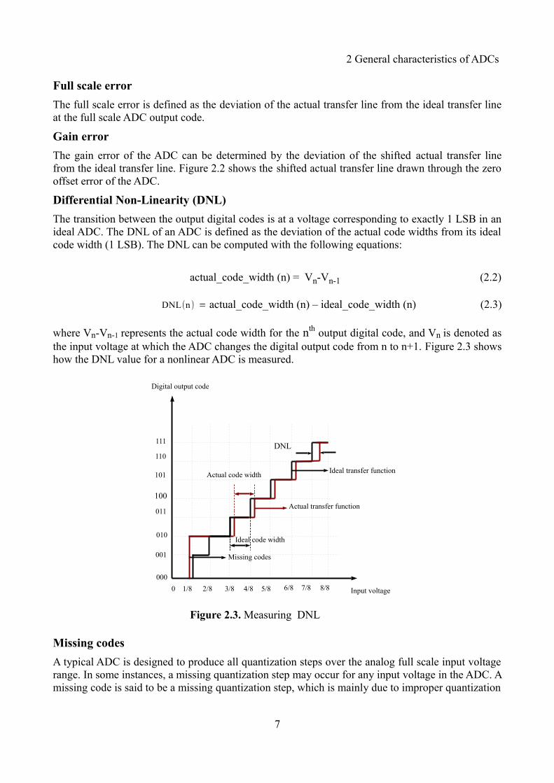
Differential Non-Linearity (DNL)
The transition between the output digital codes is at a voltage corresponding to exactly 1 LSB in anideal ADC. The DNL of an ADC is defined as the deviation of the actual code widths from its idealcode width (1 LSB). The DNL can be computed with the following equations:
actual_code_width (n) = Vn-Vn-1 (2.2)
DNL(n) = actual_code_width (n) – ideal_code_width (n) (2.3)
where Vn-Vn-1 represents the actual code width for the nth output digital code, and Vn is denoted asthe input voltage at which the ADC changes the digital output code from n to n+1. Figure 2.3 showshow the DNL value for a nonlinear ADC is measured.
Missing codes
A typical ADC is designed to produce all quantization steps over the analog full scale input voltagerange. In some instances, a missing quantization step may occur for any input voltage in the ADC. Amissing code is said to be a missing quantization step, which is mainly due to improper quantization
7
Figure 2.3. Measuring DNL
Input voltage 1/8 2/8 3/8 5/84/8 6/8 7/8 8/80
Ideal transfer function
Missing codes
Actual transfer function
Actual code width
000
001
010
011
101
110
111
100
DNL
Digital output code
Ideal code width
2 General characteristics of ADCs
and nonlinear properties of the ADC. A missing code can be seen if the DNL is -1 LSB or less forthat corresponding code.
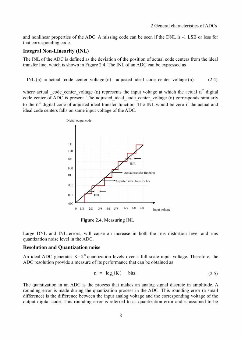
Integral Non-Linearity (INL)
The INL of the ADC is defined as the deviation of the position of actual code centers from the idealtransfer line, which is shown in Figure 2.4. The INL of an ADC can be expressed as
INL (n) = actual _code_center_voltage (n) – adjusted_ideal_code_center_voltage (n) (2.4)
where actual _code_center_voltage (n) represents the input voltage at which the actual nth digitalcode center of ADC is present. The adjusted_ideal_code_center_voltage (n) corresponds similarlyto the nth digital code of adjusted ideal transfer function. The INL would be zero if the actual andideal code centers falls on same input voltage of the ADC.
Large DNL and INL errors, will cause an increase in both the rms distortion level and rmsquantization noise level in the ADC.
Resolution and Quantization noise
An ideal ADC generates K= 2n quantization levels over a full scale input voltage. Therefore, theADC resolution provide a measure of its performance that can be obtained as
n = log2(K ) bits. (2.5)
The quantization in an ADC is the process that makes an analog signal discrete in amplitude. Arounding error is made during the quantization process in the ADC. This rounding error (a smalldifference) is the difference between the input analog voltage and the corresponding voltage of theoutput digital code. This rounding error is referred to as quantization error and is assumed to be
8
Figure 2.4. Measuring INL
Input voltage 1/8 2/8 3/8 5/84/8 6/8 7/8 8/80
Adjusted ideal transfer line
Actual transfer function
000
001
010
011
101
110
111
100
INL
Digital output code
INL

2 General characteristics of ADCs
±0.5LSB as depicted in Figure 2.5. The quantization errors in the ADC functionality behave likequantization noise. In theory, the signal to quantization noise of the ideal ADC can be summarizedusing the following equations.
The rms value of the full scale input voltage of an ADC is equivalent to
V rms =VFs
2√2. (2.6)
Using equation 2.1, the rms value of the full scale input voltage can also be written in terms of theADC least-significant-bit voltage as
V rms =VFS
(2√2)= 2n VQ
(2√2) (2.7)
where VQ=VFS
2nrepresents the quantization step voltage of the ADC.
Assume that the quantization error voltage is uniformly distributed between +1/2 and −1 /2LSB inthe ideal ADC. The term (E(ϵ2)) represents the quantization error voltage of the ADC. This can beestimated using the following equation as
E(ϵ2) =1
VQ∫
−12
VQ
+12 VQ
ϵ2d ϵ =VQ
2
12 (2.8)
E(ϵ)rms = √E(ϵ2) = √ VQ
2
12=
VQ
√12. (2.9)
Assuming that this quantization noise is the only noise introduced by the ideal ADC, then thesignal-to-quantization noise ratio [4] for such an ADC can be simplified as
9
Figure 2.5. Quantization error voltage for 3-bit ideal ADC
Analog input voltage
Quantization error in LSB
+0.5
-0.5
0
1/8 2/8 3/8 5/84/8 6/8 7/8 8/80

2 General characteristics of ADCs
SQNR = 10 log10(Ps
Pn
) = 20 log10(Srms
N rms
) = 20 log10(Vrms
E(ϵ)rms
) (2.10)
SQNR = 20 log10(V rms
√E(ϵ2)) =
2n VQ/(2√2)
VQ/√12 (2.11)
SQNR(dB) = 20 log10(2n)+20 log10(√ 3
2) ≈ (6.02×n+1.76) . (2.12)
Therefore, the signal-to-noise ratio of an ideal ADC due to quantization noise can be obtained by itsresolution.
Dynamic range
The dynamic range of the ADC is the ratio of the largest output digital code obtained at the full-scale input voltage to the smallest output digital code obtained at the lowest input voltage value ofthe ADC. The largest output digital code is 2n−1 and the smallest output digital code is 0. Then,dynamic range of ADC in dB is expressed as
DR = 20 log10((2n )
1) = 20log10(2n ) dB. (2.13)
On the other hand, the dynamic range can also specify the total number of quantization steps overan input signal voltage range of the ADC.
2.2 Frequency-domain dynamic parameters
As mentioned previously in section 2.1, the static analysis reveals the ADC performance at very lowfrequencies. Usually, dynamic testing for data converters is important to verify the performance ofmixed signal processing systems in high-speed applications. During the analog to digital signalconversion, the quantization noise, circuit mismatches, and sampling clock deviations may degradethe performance of such systems. The dynamic test of ADCs is used to evaluate the signal to noiselevels in the output frequency spectrum by applying an analog signal. The dynamic parameters ofan ADC are usually defined in a power spectrum density (PSD) plot, which can be computed byusing an M-point FFT or DFT of the output data. The acquired output sampled data (digital signal)generally contains the input sinusoidal signal frequency information, intermodulation products,harmonics, and the noise level that must be analyzed to characterize the ADC. The FFT of the twotone test is used to describe the intermodulation distortion products' spectrum for second-order andthird-order harmonic products. The following discussion provides the mathematical modelcalculations that are used to compute the important dynamic parameters of ADCs. As an example,the ADC PSD plot (Figure 2.6) illustrates the dynamic performance metrics.
10

2 General characteristics of ADCs
Signal-to-Noise Ratio (SNR)
The ADC signal-to-noise ratio is the ratio between the rms signal level and the rms total outputnoise level, where the output noise includes all the noise sources present in the ADC likequantization noise, clock jitter, excluding the harmonics of test tone signal. In general, the SNR ofthe ADC can be computed as
SNR (dB) = 10 log10(Ps
Pn
) = 20 log10(Srms
N rms
) (2.14)
where Srms and Nrms are the rms levels of signal (1st harmonic) and noise respectively, whereas Ps
and Pn denotes the rms signal power and rms noise power.
Total Harmonic Distortion (THD)
The THD of an ADC is usually defined as the ratio of the rms power of the signal to the rms powersum of all the harmonic components of the signal. This can be expressed as
THD(dBc) = 20 log10(Srms
Drms
) (2.15)
where Drms represents the rms level of all harmonic components of the signal in the outputfrequency spectrum.
Signal-to-Noise-and-Distortion Ratio (SNDR)
SNDR is the combination of SNR and THD of the ADC, and can be expressed as the ratio of rmspower of signal to the rms power of all other spectral components in the frequency spectrum,including harmonics of the test tone signal but excluding the DC component in the output frequencyspectrum of the ADC. The ADC SNDR can be expressed as
11
Figure 2.6. Power spectrum density plot for an ADC
Frequency (MHz)
3rd harmonic
Power spectral density Po
wer
(dB
)
0 10 20 30 40 50 60 70
0
-20
-40
-60
-80
-100
SNR
SNDR SFDRTest tone (1st harmonic)
2nd harmonic
Strongest spurious tone
RMS noise and distortion level
RMS noise level

2 General characteristics of ADCs
SNDR(dB) = 20 log10(S rms
N rms+Drms
) (2.16)
where Srms is the rms signal level, Nrms is the rms level of noise and Drms describes the rms level ofall harmonic components of the test tone.
Effective Number Of Bits (ENOB)
The ENOB is one of the important specifications of the ADC measurement in bits. It provides theoutput ADC resolution. Generally, the ENOB can be expressed in terms of SNDR of the ADC. TheSNDR denotes the signal versus all nonlinear effects and noise sources present in the ADCfrequency spectrum. Consider an ideal ADC that would have only quantization noise where SNDRcan be defined as the SQNR for its resolution. Therefore, ENOB of an ideal ADC can be written as
ENOB(bits) =[SNDR−1.76 dB]
6.02. (2.17)
Spurious Free Dynamic Range (SFDR)
The SFDR is defined as the ratio of the rms power of signal to the rms power of the strongestspurious spectral component (peak harmonic component) in the ADC output frequency spectrum.The spurs appear at the harmonics of the applied input signal (test tone) due to the nonlinear effectsof the ADC. This can be expressed as
SFDR (dBc) = 20 log10(S rms
D 1rms
) (2.18)
where Srms depicts the rms value of signal and D1rms represents the rms value of next strongestspurious component in the ADC output frequency spectrum.
Intermodulation Distortion (IMD)
Two or more input signals are applied to an ADC that could generate the intermodulation distortionproducts. An IMD test in the ADC is used to enumerate the additional signals (sum and differenceof the input signal frequencies) in the ADC output frequency spectrum. These IMD products areproduced by the intermodulation of the input signal frequency components and the ADCnonlinearities. These tests are often used in ADC design to assess the limits of input signal dynamicrange and to characterize the ADC linearity. IMD tests are usually measured with two or more inputanalog signals with the same amplitude.
Consider the example in Figure 2.7, which shows the two tone output spectrum of the ADC thatillustrates the intermodulation distortion products. The input signal frequencies F1 and F2 of theADC produce the fundamental frequencies and harmonic components. As well, new frequencycomponents appear at the sum and difference of these input signal frequencies. The frequency ofintermodulation distortion products for a two tone test can be formulated as
F(IMD) = m F1+n F2 (2.19)
where n and m are integer numbers. For example, the terms F1+F2, and F1+F2 denotes the second
12

2 General characteristics of ADCs
order distortion products of the ADC. The third order distortion products are represented as theterms 2 F1+F2 , 2 F1−F2 and F1−2F2 .
Aliasing
In the case of ADC, the input signal is sampled according to the Nyquist-Shannon criterion, whichis defined as Fs>2Fb, where Fs represents the sampling frequency and Fb defines the signalbandwidth of interest. The term 2Fb represents the Nyquist-rate. Aliasing occurs if the input signalof the ADC is sampled at lower than the Nyquist-rate, i.e., Fs<2Fb. Due to aliasing effects of theADC, the unwanted signal frequencies appear besides the desired input signal frequency in theoutput frequency spectrum.
2.3 Oversampling and noise shaping property
According to the sampling rate of ADCs they can also be classified as Nyquist-rate ADCs oroversampling ADCs. The Nyquist-rate ADCs are sampling the input signal at a minimum requiredrate on the basis of the given signal bandwidth, whereas the oversampling ADCs samples the inputsignal at a rate higher than the Nyquist-rate. The ratio between the sampling rate of an input signalin the oversampling ADC and the Nyquist-rate ADC is denoted as the Over Sampling Ratio (OSR).The power spectral distribution of quantization noise within the ADC bandwidth is shown in Figure2.8 and Figure 2.9. A nice advantage of oversampled ADCs is that they reduce the quantizationnoise level in the signal band of interest. Furthermore, the quantization noise as well other noise canbe separated from the signal band by using digital filters (decimation filter) after the analog todigital signal conversion, so that it is possible to obtain good SNR and resolution of the digitalsignal. Moreover, oversampling of an input signal along with the noise shaping property of the ADCrelaxes the digital filter complexity.
13
Figure 2.7. Two-tone IMD spectrum
Frequency (MHz)
IMD spectrum with 2nd and 3rd Order IMD products
Pow
er (
dB)
0 10 20 30 40 50 60 70
0
-20
-40
-60
-80
-100
F1 F
2
F1+F
2 F
1-F
2
2 F1- F
22F
2- F
1
2 F1 2F
2
F1, F
2 - Input tones
F1+/- F
2 - 2nd Order IMD products
2F1+/- F
2, F
1+/- 2F
2 -3rd
Order IMD products

2 General characteristics of ADCs
14
Figure 2.8. Spectral distribution of quantization noise in Nyquist-rate ADCs
Noise
Power spectral density of quantization noise
Frequency
Nyquist rate sampling at Fs
Band of interest
0 Fs/2 F
s OSR*(F
s/2)
Figure 2.9. Spectral distribution of quantization noise in oversampling ADCs
Oversampling at OSR*Fs with noise shaping property
Power spectral density of quantization noise
Frequency
Noise
Band of interest
0 Fs/2 F
s OSR*(F
s/2)
Power spectral density of quantization noise
Frequency
Noise
Oversampling at OSR*Fs
Band of interest
0 Fs/2 F
s OSR*(F
s/2)
3 VCO-based ADC
3 VCO-based ADC
This chapter focuses on the different architectures and the working principle of an ideal VCO-basedADC. In addition, this chapter presents an extensive description of the theoretical analysis of thenonideality effects on the VCO-based ADC performance. The nonidealities mainly include phasenoise, sampling clock jitter, flip-flop metastability as well as other aspects that are involved in theVCO-based ADC performance.
3.1 Introduction to VCO-based ADCs
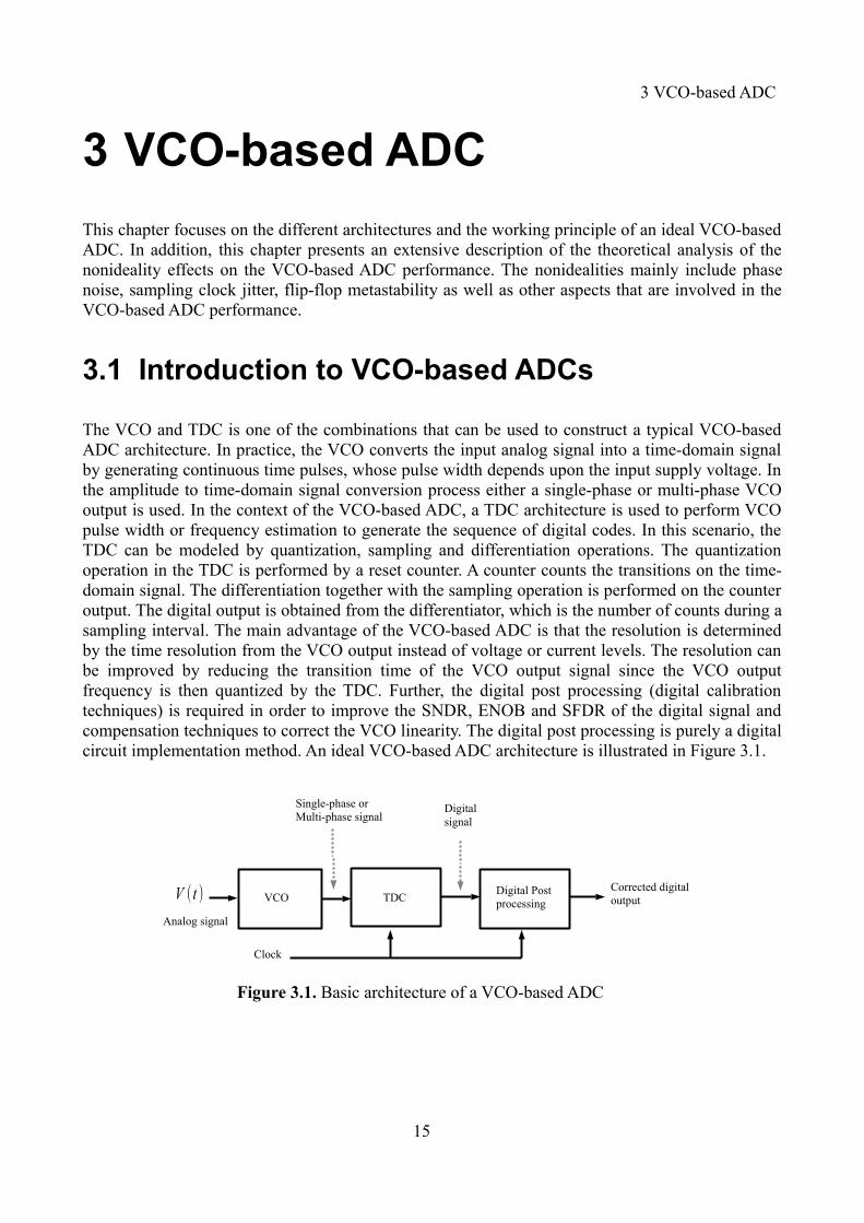
The VCO and TDC is one of the combinations that can be used to construct a typical VCO-basedADC architecture. In practice, the VCO converts the input analog signal into a time-domain signalby generating continuous time pulses, whose pulse width depends upon the input supply voltage. Inthe amplitude to time-domain signal conversion process either a single-phase or multi-phase VCOoutput is used. In the context of the VCO-based ADC, a TDC architecture is used to perform VCOpulse width or frequency estimation to generate the sequence of digital codes. In this scenario, theTDC can be modeled by quantization, sampling and differentiation operations. The quantizationoperation in the TDC is performed by a reset counter. A counter counts the transitions on the time-domain signal. The differentiation together with the sampling operation is performed on the counteroutput. The digital output is obtained from the differentiator, which is the number of counts during asampling interval. The main advantage of the VCO-based ADC is that the resolution is determinedby the time resolution from the VCO output instead of voltage or current levels. The resolution canbe improved by reducing the transition time of the VCO output signal since the VCO outputfrequency is then quantized by the TDC. Further, the digital post processing (digital calibrationtechniques) is required in order to improve the SNDR, ENOB and SFDR of the digital signal andcompensation techniques to correct the VCO linearity. The digital post processing is purely a digitalcircuit implementation method. An ideal VCO-based ADC architecture is illustrated in Figure 3.1.
15
Figure 3.1. Basic architecture of a VCO-based ADC
V (t ) VCO Digital Post processingTDC
Corrected digitaloutput
Digital signal
Single-phase orMulti-phase signal
Analog signal
Clock

3 VCO-based ADC
3.2 Architectures
Several articles and journals have been published regarding the attractive properties, architectures,and performance summaries of the VCO-based ADC. The major architectures for data conversionsusing VCO-based ADC are listed below:
• Single-phase with single-bit quantization
• Single-phase with multi-bit quantization
• Multi-phase with single-bit quantization
• Multi-phase with multi-bit quantization
The single-bit quantization circuit can be carried out by 1-bit registers. In contrast, multi-bitquantization requires a counter, which could be used to detect the switching events occurring at theVCO output phases. This section distinguishes the background theory of single-phase and multi-phase with the single-bit and multi-bit quantization architectures.
3.2.1 Single-phase VCO-based ADC
A single-phase with multi-bit quantization architecture includes only a single-phase VCO outputsignal. An ideal single-phase VCO-based ADC architecture [5] is shown in Figure 3.2. Theoperation is depicted in Figure 3.3, which shows that the counter counts the rising edges of thesingle-phase time-domain signal from the VCO output. The sampling register captures the counteroutput at the rising edge of the sampling clock and its output is then forwarded to another register atthe next rising edge of the sampling clock. The digital output is obtained by the subtraction of thetwo consequent sampled counter output values. In a multi-bit quantization architecture of the VCO-based ADC, the resolution can be improved by the counter that counts the number of both rising andfalling edges of the single-phase VCO output signal. The lower limit on the sampling frequencyshould be chosen based on counter width. The sampling frequency in multi-bit quantization can bemeasured using the equation
Fs >max (f vco)
2KCNTR−1 (3.1)
where f vco represents the VCO oscillation frequency, and KCNTR is the counter word length.
16
Figure 3.2. Single-phase with multi-bit quantization architecture
Sampling clock
VCO
Digital output
ϕ 1Register Counter
+
- y i
+Analog signal
RegisterV (t)

3 VCO-based ADC
3.2.2 Multi-phase VCO-based ADC
In order to obtain a high time resolution, the multi-phase time-domain signal from the VCO outputcan be used in the VCO-based ADC. In this architecture, each phase of the VCO output time-domain signal is processed by the QSD (Quantizer, Sampler and Differentiator) block. As a result,the time resolution will improve compared to the signal-phase VCO-based ADC. An example of anideal multi-phase VCO-based ADC architecture is illustrated in Figure 3.4 [5]. A typical QSD canbe distinguished as a single-bit QSD or a multi-bit QSD architecture. Using a multi-phase VCOwith single-bit quantization architecture makes it simple to implement a high speed VCO-basedADC in such a way that the counters are avoided, since its functionality is based on one samplingper edge.
An example of single-bit quantization architecture is shown in Figure 3.5 [5]. The QSD architectureis typically made with two flip-flops and one XOR gate for comparison of two sampled outputs. Inthis case, the QSD block captures the progress of rising edges or falling edges of the VCO outputphase during a sampling clock period. In order to generate the digital code, the sampling frequencyshould be chosen to capture the progress of the VCO phase in one sampling period. In addition, the
17
Vcntrl
VCO output
Sample clock
Counter
Digital output
Figure. 3.3. Operation of the single phase VCO based Quantizer
4 8 2
Figure 3.4. Multi-phase VCO-based ADC architecture
Y[k]
QSD
QSD
QSD
Analog signal
ϕ 1
ϕ 2
ϕ N
+VCOV (t )Digital output
Vcntrl
VCO output
Sample clock
Counter
Digital output
Figure 3.3. Operation of single-phase VCO-based quantizer
4 8 2

3 VCO-based ADC
sampling frequency is higher than twice the maximum possible VCO output frequency in thesingle-bit quantization. The lower limit on the sampling frequency Fs in single-phase VCO-basedADC can be written as
Fs ⩾ 2max( f vco)
(3.2)
where Fs is higher than twice the possible maximum output frequency (f vco) of the VCO phasesignal needed to detect one rising edge or falling edge within one sampling period.
A simple multi-bit quantization architecture is shown in Figure 3.6. A counter counts the maximum2KCNTR−1 rising edges or falling edges of the VCO output phase in the multi-bit quantizer. Hence,the minimum sampling frequency that can be used in the multi-phase with multi-bit quantizationarchitecture is given by
Fs ⩾max(f vco)
2K CNTR−1 (3.3)
where f vco represents the VCO oscillation frequency, and KCNTR is the counter word length.
A multi-phase VCO-based ADC circuit occupies a large chip area and increases the powerconsumption due to an increased number of counters and VCO phases when compared to thesingle-phase VCO-based ADC architecture. The presence of non-idealities such as flip-flopmetastability, sampling clock jitter and VCO delay cell mismatches may degrade the VCO-basedADC functionality.
18
Figure 3.6. Multi-bit quantization architecture
Register
Sampling clock
ϕ i RegisterCounter
-y i
+
VCO phase signal Digital output
+
Figure 3.5. Single-bit quantization architecture
Sampling clock
ϕ iy i
Digital output
XORDFFDFF
VCO phase signal

3 VCO-based ADC
3.3 Voltage-controlled oscillator
The Voltage-Control Oscillator (VCO) is used to convert the voltage-domain analog signal into aphase-domain signal, which is a time-based signal. In general, the VCO definition [6] is given as
f vco = f 0+K vco Vcntrl( t ) (3.4)
where f o is the center oscillation frequency of the VCO, K vco represents the VCO gain and V cntrl(t)denotes the input analog signal. The above equation 3.4 represents the input voltage to frequencyrelationship of an ideal VCO and whose output frequency is proportional to the input signal voltage.In addition, the time-domain of the VCO output phase is continuous and acts as a continuous timevoltage to phase integrator.
Tuning range
The VCO tuning gain as well a wide frequency tuning range are the main attributes of a typicalVCO design. From equation 3.4, an ideal VCO output frequency is a linear function of its inputvoltage, which is illustrated in Figure 3.7. The tuning curve may not be linear in the practical VCO,which is also depicted in Figure 3.7. The K vco nonlinearity of VCO generates the higher orderharmonics in the phase output.
In Figure 3.7, v1 and v2 are represented as input control voltage limits. The tuning range defines thedifference between the f 1 and f 2 of the VCO output frequencies, and VCO gain (K vco) is defined as
Kvco ≥f 2−f 1
v2−v1
Hz /V . (3.5)
In order to convert the input voltage to a time-based signal, a ring-oscillator can be used as a VCO.In a multi-phase VCO-based ADC, the ring-oscillator can be designed by cascading the delay cellsto provide the multiple phases of the output signal.
19
Figure 3.7. Ideal vs. non-ideal VCO tuning curve
Ideal linear VCO
Nonlinear VCO Frequency
Control voltage
Kvco
linear range f
1
f2
v1 v
2

3 VCO-based ADC
3.4 Basic working principles
The basic principle of a VCO-based ADC is associated with the VCO functionality as well thequantization and sampling process of the time-domain signal from the VCO output. A nonlinearbehavioral frequency domain model of the VCO-based ADC [5][7] is shown in Figure 3.8. Theworking principle of VCO-based ADC can be expressed by the following mathematical analysisbased on [5]. In general, the voltage-controlled oscillator generates a phase information signal froma voltage-domain analog signal.
Let us assume that an N-stage ring-oscillator is an ideal linear VCO, and its input signal V cntrl(t) is a
sinusoidal signal with amplitude A and frequency Fin.
Therefore, V cntrl(t ) = A cos (2 πf i n t). (3.6)
The input voltage to frequency transfer function of the ideal VCO can be expressed as
ψ (u) = 2π (Kvco Vcntrl(t )+f c)
(3.7)
where K vco denotes the VCO gain and f c is the center frequency of the VCO.
The phase signal Фt( t) from the VCO output is a continuous time-domain signal that can becomputed as the time integral of voltage to frequency transfer function, i.e.,
Фt( t) = ∫ψ(u )dt . (3.8)
The VCO output phase in the k th sampling period can be expressed as
Фt [k ] = ∫0
kTS
ψ (u)dt = ∫0
kTS
2π (K vco V cntrl+ f c )dt . (3.9)
20
Figure 3.8. Working principle of an ideal VCO-based ADC
F
Input spectrum
F
Input harmonics
F F F
VCO noise Quantization noise Output spectrum
y[k]Q
Frequency to phase Quantizer Sampler Digital output
ΔK vco
Фt( t) Фq(t )
F s
1−z−12πs
V cntrl( t)Фq[k ]

3 VCO-based ADC
The output phase signal (Фt( t)) is quantized by 2 π/ NФ , where NΦ specifies the equi-distant Nnumber of VCO phases. The resulting quantized phase signal Фq (t) is then sampled at a frequencyFs=1 /T s to generate the sequence of discrete values (Фq [k ]). The digital output can be obtained bythe first order difference of this sequence. The digital output for the VCO-based ADC can beexpressed by the following equation [5],
y [ k ] =NФ
2 π(Фq [k ]−Фq [k−1]) =
NФ
2 π(ΔФt [k ]− ΔФε [k ]) (3.10)
where Фq[ k ], Фq[ k−1] are called the quantized VCO output phase in the k th sampling period, andits preceding sampling period respectively. The term Δ is the symbol for the backward differenceoperator.
The term ΔФt [k ] defines the VCO phase changes during the k th sampling period and can be computed as
ΔФt [k ] = ∫(K−1 )TS
KTS
ψ(u )dt = ∫(K−1)TS
KTS
2π (Kvco Vcntrl+f c)dt . (3.11)
Therefore, the above equation 3.11 can be computed as
ΔФt [k ] = 2πKvco A Tssinc(f i n Ts)cos (2π f i n(k Ts−Ts
2))+f c Ts . (3.12)
The above expression infers the input signal amplitude of the VCO in phase-domain within asampling period to be a sinc function of the input signal frequency (f i n) . In addition, thesinc(f i n Ts) function is defined as sin(π f i n Ts)/(π f i n Ts). The second and higher order harmonicsin the phase output are attenuated by inherent sinc anti-alias filtering of the VCO.
The quantization error Фε [k ] in the k th sample period is given by
Фε[k ] = Фt[ k ]−Фq [k ] . (3.13)
Hence, the digital output for the VCO-based ADC within the k th sampling interval can beapproximated by the expression [9]
y [ k ] = NФ Ts K vcosinc (f i n Ts)Vcntrl(kTS−TS
2)+B+e[k ] (3.14)
where B = NФ f c Ts
(3.15)
e [k ] = −NФ
2 π∇ Фε [k ] . (3.16)
21
3 VCO-based ADC
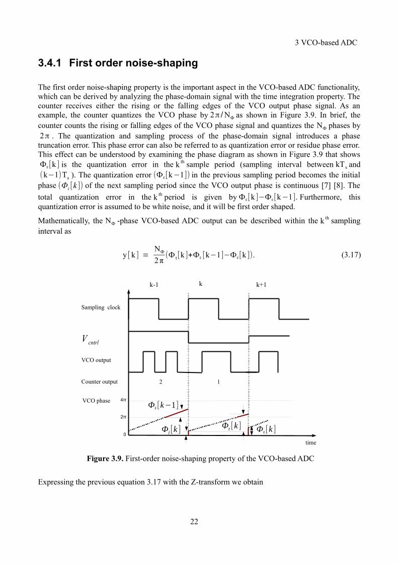
3.4.1 First order noise-shaping
The first order noise-shaping property is the important aspect in the VCO-based ADC functionality,which can be derived by analyzing the phase-domain signal with the time integration property. Thecounter receives either the rising or the falling edges of the VCO output phase signal. As anexample, the counter quantizes the VCO phase by 2π / NФ as shown in Figure 3.9. In brief, thecounter counts the rising or falling edges of the VCO phase signal and quantizes the NФ phases by2π . The quantization and sampling process of the phase-domain signal introduces a phasetruncation error. This phase error can also be referred to as quantization error or residue phase error.This effect can be understood by examining the phase diagram as shown in Figure 3.9 that showsФε[k ] is the quantization error in the k th sample period (sampling interval between kT s and(k−1)Ts ). The quantization error (Фε[k−1]) in the previous sampling period becomes the initialphase (Фi [k ]) of the next sampling period since the VCO output phase is continuous [7] [8]. The
total quantization error in the k th period is given by Фε[k ]−Фε[k−1]. Furthermore, thisquantization error is assumed to be white noise, and it will be first order shaped.
Mathematically, the NФ -phase VCO-based ADC output can be described within the k th samplinginterval as
y [ k ] =NФ
2 π(Ф t [k ]+Фε [k−1]−Фε[k ]). (3.17)
Expressing the previous equation 3.17 with the Z-transform we obtain
22
Figure 3.9. First-order noise-shaping property of the VCO-based ADC
Counter output 2 1
4π
2π
0
VCO phase
V cntrl
VCO output
Sampling clock
k-1 k k+1
Фε[k−1]
Фε[k ]Фt [k ]Фi [k ]
time
3 VCO-based ADC
Y (z) =NФ
2 π(Ψt (z)−(1−z−1
)Ψ ε(z )) . (3.18)
From the above expression, we can notice that the noise transfer function (1−z−1)Ψε yields the firstorder noise shaping of the quantization noise of the VCO-based ADC. The quantization noise canbe varied by the position of the sampling clock edges on the VCO output phase domain signal [8].
3.4.2 Quantizer resolution
An ideal VCO-based ADC resolution can be determined by the VCO tuning range together with thetotal number of VCO phases and the sampling frequency (Fs) respectively. The VCO-based ADChas prioritized the time-based signal resolution generated from the VCO output phase over the inputvoltage-domain signal. The resolution for multi-phase VCO-based ADC that uses a counter as aphase quantizer from [9] can be described as
MQ = log2
f tune
Fs
+ log2 NΦ (3.19)
where MQ gives the resolution of the VCO-based ADC and NΦ represents the number of total delaycells in the VCO (ring-oscillator).
The term f tune in equation 3.19 represents the VCO tuning range, which is defined by the differencebetween the minimum and maximum output frequencies of the VCO. Thus,
f tune = f 2−f 1 (3.20)
where f1 and f2 are defined as the upper and lower limit of the VCO frequency, and MQ is given by
MQ = log2(f 2−f 1)
NΦ
Fs
. (3.21)
It can be seen that the MQ is determined by the VCO tuning range for a given sampling frequency
Fs. The VCO tuning range f tune can assume the full scale of the VCO-based ADC to be digitized.The resolution of the ADC can be improved by increasing the number of VCO phases in deepsubmicron CMOS technologies. Note that, the VCO tuning range may decrease by increasing theVCO phases (adding delay cells).
3.5 Non-ideal effects of the VCO-based ADC
This section describes the impact of nonidealities such as the VCO nonlinearity, VCO delay cellmismatches, sampling clock jitter and flip-flop metastability on the VCO-based ADC [8].
23

3 VCO-based ADC
3.5.1 VCO nonlinearity
A VCO with nonlinearity in the required frequency range generates unwanted harmonics such asspurs in the output frequency spectrum. This has an effect that is critical to the VCO-based ADCfunctionality, which degrades the SNDR, SFDR and overall ADC performance. Consider a case inwhich a polynomial function for the nonlinear VCO transfer function is modeled as
ψ (u) = 2π×(f o+Kvco V cntrl(t)+C2×V cntrl2
( t)+C3×Vcntrl3
( t ).........) (3.22)
where ψ (u) represents the voltage-to-frequency transfer function of the nonlinear VCO.
The phase-domain signal [8] due to the nonlinear behavior effect of the VCO can be expressed as
Ф[k ]t , nl = ∫(k−1)TS
kTS
2 π (Kvco V cntrl( t)+f o+C2 V cntrl2 (t)+C3 V cntrl
3 (t) ......)dt (3.23)
where V cntrl(t)=A sin(2π f i n t ) .
The nonlinearity factor of a VCO [9] in the frequency tuning range at a particular voltage of theinput signal (Vcntrl) is identified as
nonlinearity (%) = (3.24)
In the above expression, f k is called the ideal VCO output frequency and f k ' represents thenonlinear VCO output frequency for an input DC voltage (i .e .,V cntrl=Vk). The presence of theVCO nonlinearity characteristics limits the input dynamic range of the ADC. In addition, itdegrades the resolution and SNDR of the digital signal. The VCO higher order harmonics can beminimized by a small input signal amplitude. In order to achieve a high VCO linearity,compensation techniques could be used in the VCO-based ADC.
3.5.2 VCO phase noise
Generally, a VCO is chosen to provide low phase noise and high tuning range. If noise is added tothe input signal, then the required VCO output frequency will vary. The VCO output phase signalwill be affected due to the phase noise, which is modeled by applying a small amount of the inputreferred noise in the VCO. The voltage to frequency transfer function (ψ (u)) of the VCO can berepresented as
ψ (u)=2 π (Kvco Vcntrl( t )+ f o+Kvco Vn( t)) (3.25)
where V n( t) is the input noise source of the VCO.
Therefore, the input phase change due to noise sources of the VCO [7] can be expressed as
24
f k−f k '
f k
×100.
3 VCO-based ADC
Фt , pn [ k] = ∫(k−1)TS
kTS
2π (KVCO Vcntrl( t)+ f o+KVCO Vn( t))dt (3.26)
Фt , pn [k ] = Ф t [k ]+ ∫(k−1)TS
kTS
2 π(KVCO Vn( t))dt (3.27)
Фt , pn [ k] = Фt [k ]+Фpn [k Ts]−Фpn[(k−1)T s] (3.28)
where Фpn [k ] is the phase noise from VCO output and Фt [k ] represents the VCO output phase progression during the k th sampling period and is expressed by
Фt [k ] = ∫(k−1)TS
kTS
2 π(KVCO Vcntrl( t))dt . (3.29)
The Z transform of above equation 3.28 is given by
Фt , pn(z) = Ф t(z )+(z−1)Фpn(z) . (3.30)
The above expression suggests that the VCO integration within the sampling clock boundsdetermines the first order noise shaping property of the quantization. The SNR of the VCO-basedADC due to the VCO phase noise can be measured by using the output phase signal [8].
Thus, SNRtpn = 10 log10
PΦ, t
PΦ, pn
. (3.31)
3.5.3 Mismatch of VCO delay cells
In practice, the delay cells are those of a ring-oscillator and generates rising and falling edges thatare equally spread over time. Consider a case where a mismatch of the delay cells causes anuncertainty in their propagation delay. The mismatches could be due to device size variations,supply voltage variations and temperature variations. As a result, the VCO-based quantizer includesa phase error in the output due to these mismatches. This phase error is further sampled and first-order shaped in the VCO-based ADC. The effect of VCO mismatches can possibly be prevented byminimizing the number of delay cells.
3.5.4 Flip-flop metastability
In the context of VCO-based ADCs, the TDC is usually implemented with D Flip-Flops (DFFs) forthe quantization and sampling operations on the VCO output signal. There is a possibility ofmetastability problem due to setup and hold time violations in a flip-flop. The following example oftiming diagrams shown in Figure 3.10 and Figure 3.11 have been used to describe metastability for
25

3 VCO-based ADC
a general D flip-flop circuit. In general, metastability occurs if the input data does not meet thesetup time (Tsu) or hold time (Th) of the D flip-flop. In Figure 3.10, Tpcq is the propagation delayand Tms represents the metastable window and Tpcq, max is denoted as the maximum tolerable clock toQ output delay. Figure 3.11 shows that the input data is received by DFFs in the metastable window.
26
Figure 3.11. The metastable window definition [7]
Setup time (Tsu
) Hold time (Th)
Propagation delay Tpcq
Propagation delay Tpcq
Tpcq,max
Tpcq,normal
Sampling clock
Metastable windowT
ms
Input data
Figure 3.10. Setup and hold-time definitions [7]
Q output
Tsu
Th
Tpcq
Input data
Sampling clock

3 VCO-based ADC
The multi-bit quantization architecture uses the counter to quantize the VCO phase signal and thenD flip-flops (multi-bit registers) are used to sample the quantized phase signal. If the counter outputdoes not meet the setup or hold timings of the D flip-flops then its output is not stable in thedifferentiation block. As a result, the differentiator generates the incorrect number of rising edges ofthe phase signal during the flip-flop metastability. Therefore, the flip-flop metastability problemmay degrade the SNR of the VCO-based ADC. An example of a timing diagram from [8] isillustrated in Figure 3.12 that shows the effect of D flip-flop metastability in a typical VCO-basedADC. Figure 3.12 shows that the differentiator output is not stable at the rising edge of the sampleclock due to the flip-flop metastability problem.
3.5.5 Sampling clock jitter
The purpose of the clock signal is to sample the phase-domain continuous time signal in a VCO-based ADC design. The sampling clock is usually periodic with a fixed period. However, it isnecessary to investigate how sampling clock deviations may influence the VCO-based ADCperformance. Consider a case where jitter is present on the sampling clock. In addition, thesampling clock jitter could be divided into absolute jitter and period jitter, respectively. In anexample, illustrated in Figure 3.13, a timing diagram is used to show the effect of the samplingclock jitter in the VCO-based ADC design.
In Figure 3.13, Taj [k ] represents the absolute error which gives the time difference in the position ofthe k th edge between the ideal clock and sample clock with jitter. The term Tpj[ k ] corresponds to theperiod jitter, and it denotes the time difference between the k th period of the ideal and the sampleclock with jitter. The VCO phase change within a sampling clock period can be quantified as
Фt [k ]= ∫kTS
(k+1)TS
ψ (u )dt. (3.32)
27
Figure 3.12. Effect of flip-flop metastability [8]
Counter output
VCO output rising edges
Differentiator output without metastability
Differentiator output with metastability
Sample clock
3 4 5 6 7 14 15 16
15-3 = 12
14-3 = 11, 14-4 = 10,15-3 = 12, 15-4 = 11, 16-4 = 12, 16-3 = 13
T ms
2
T ms
2
T ms
2
T ms
2

3 VCO-based ADC
The above equation defines the sampling clock without jitter in the k th period of the VCO phaseoutput, where ψ (u)=2π(K vco Vcntrl+f 0) is the voltage to frequency conversion function of theVCO. The sampling clock with jitter for the VCO phase-domain input signal [8] can be written as
Фt , sj[k ]= ∫kTS+T aj[ k ]
(k+1 )TS+T aj[k+1]
ψ (u)dt (3.33)
Фt , sj[k ]= ∫(k )TS+T aj[k ]
(k+1 )TS+T aj[k+1]
2 π(K vco Vcntrl+ f 0)dt . (3.34)
where Фt , sj[k ] represents the phase of the VCO due to the sampling clock jitter.
The above equation shows that the uncertainty in the sampling clock signal may degrade theperformance of the VCO-based ADC circuit.
28
Figure 3.13. Timing diagram of sampling clocks with and without jitter
Ideal sampling clock
Sampling clock with jitter
T aj[k ] T aj[k ] T pj [k ]
T aj[k+1]

4 Design
4 Design
This chapter briefly describes the VCO-based ADC that was designed as a part of this thesis work.The design has been defined in an HDL description with Mentor Graphics-ModelSim tool. TheADC was implemented using digital synthesis tools. In addition, the design was carried out onschematic and layout level. The implementation of the ADC design using digital tools is presentedin Chapter 6.
4.1 The architecture
A multi-phase VCO and multi-bit quantization architecture has been chosen for this VCO-basedADC design. A single ended 13-stage ring-oscillator offers design programmability and is used as adigital VCO. The corresponding phases of a multi-bit quantizer together with the adder block aredefined as the TDC architecture. The multi-bit quantizer sub-block has a counter and samplingblock together with the differentiator. A 4-bit quantizer has been chosen in this TDC architecture,which has fully digital and simple logic gates. A pipelining register is introduced between thesubtraction circuit and the adder block to reduce the propagation delay in the signal paths. Thedigital VCO and the TDC architectures are used to implement the VCO-based ADC that is shown inFigure 4.1. The ring-oscillator converts an analog signal into 13 time-based phases. The time-basedsignal will then be processed by a 4-bit quantization architecture. The digital code sequence isgenerated by summing all the values from the output of the 4-bit quantization stages. The powersupplies are different for the VCO and TDC blocks since the VCO directly receives the analogsignal. On the other hand, the TDC architecture needs a constant power supply. The TDC isgenerally referred to as the digital logic section of the VCO-based ADC.
29
Figure 4.1. Implemented VCO-based ADC architecture
Block1 Block2Input signal
Sample clock
4-bitCounter
4-bitDFF
4-bitSubtractor
Sample clock
4-bitCounter
4-bitSubtractor
Adder
4-bitDFF
4-bitDFF
4-bitDFF
8-bit Digital code
4-bitDFF
0
1
12

4 Design
4.2 Ring-oscillator as a VCO
According to the thesis requirements, the synthesis should use a fully digital ring-oscillator as aVCO. Moreover, each delay cell in the ring-oscillator appears as a simple CMOS inverter. The VCOoscillation frequency is varied by controlling its voltage supply. Therefore, its output frequency andtuning range is the function of control voltage and delay cell geometrical dimensions.
Fvco vs. Vcntrl tuning curve
The frequency tuning range and linear behavior are important concerns of VCO-based ADC design.The ring-oscillator output frequency stability is affected by many factors including power supplyvariations, process parameter variations, and temperature. The VCO linear behavior can bedetermined by plotting the tuning characteristics, which is shown in Figure 4.2. The tuning curveshows that the voltage to frequency conversion is nonlinear for the 0.4 to 1.4 V voltage range.Hence, the VCO nonlinear characteristics generate the high order harmonics and typically degradethe VCO-based ADC performance. The VCO tuning range has been plotted between voltages 0.65to 1.35 V and the frequency tuning range between 102.8 and 1037 MHz. The implemented VCOgain can be calculated using
K vco ≥F2−F1
V1−V2
=1.037 G−102.8 M
1.35−0.65= 1.334 GHz / V. (4.1)
The VCO linearity in this selected frequency span of 102.8 to 1037 MHz improves by limiting theinput voltage to 0.65 to 1.35 V input voltage.
30
Figure 4.2. VCO tuning characteristics

4 Design
4.3 Counter design
A 4-bit synchronous upcounter is implemented in the multi-bit quantization block to obtain amaximum of 16 states (e.g., 2K CNTR=16 , and KCNTR=4 ). The counter counts the rising events on theVCO output phase signal and produces the output from 0 to 15. The external reset pulse is used toreset the counter operation in the designed VCO-based ADC.
4.4 Differentiator
The function of the differentiator block is illustrated in Figure 4.3 that consists of a combination oftwo 4-bit registers and one differentiator. The first register represents the sampling register, whichcaptures the counter output at a rising edge of the sampling clock. The input to the second register isthe output of the first register at the next rising edge of that sampling clock. Therefore, the numberof VCO phase rising edges in one sample clock period is the difference between these twoconsecutive samples. The count value in the sampling period should not overflow since the ADCoutput will be erroneous. This leads to that a number of VCO rising edges in one sampling clockperiod should be equal or less than 2KCNTR−1 at maximum VCO output frequency, which is the lowerlimit on sampling frequency of the VCO-based ADC design. The minimum sampling frequency canbe expressed as
Fs ⩾max(f vco)
2K CNTR−1 (4.2)
where max (f vco) is the highest possible ring-oscillator output frequency.
The upper limit on the sampling frequency is given as the frequency at which any of thedifferentiator stages in the VCO-based ADC design are not able to capture a single rising edgewithin one sampling interval at the minimum ring-oscillator output frequency. This can beexpressed as
2 NΦ min (f vco) ⩾ Fs ⩾max(f vco)
2(K CNTR)−1 (4.3)
where min (f vco) is the lowest possible ring-oscillator output frequency and N Φ represents thenumber of VCO phases.
31
Figure 4.3. The differentiator circuit
4-bi
t reg
iste
r
4-bi
t reg
iste
r
Sampling clock
Input
+
- + Output

4 Design
4.5 Adder array
The adder array sums all the 13 stages of the 4-bit quantizer output values, and produces an 8-bitcorresponding binary output. There is an advantage in using the synthesis tool in that itautomatically picks an optimized minimum delay structure for an arithmetic expression in the HDL.According to the design constraints, the synthesis tool generates an area-efficient adder array. Thearithmetic expression describes the merging of 4-bit cascaded adders. An 8-bit adder tree isdepicted in Figure 4.4. The tool uses temporary registers to store the intermediate results during theaddition operation. In addition, it determines an N-bit dummy variable for rearranging thearithmetic operators for the cascaded adder tree.
Z [7:0] <= D0 [3:0]+ D1 [3:0] + D2 [3:0] + D3 [3:0]…..... D12 [3:0] (4.4)
32
Figure 4.4. The cascaded adders structure
+
+
D0 [3:0] D1 [3:0]
D2 [3:0]
+
D3 [3:0]
+
D12 [3:0]
Z [7:0], carry_out
N-bit temporary variable
N-bit temporary variable
N-bit temporary variable
5 Simulation results
5 Simulation results
This section presents the simulation results of the VCO-based ADC implemented on the transistorlevel. The Cadence Spectre simulator has been used in this thesis work for the circuit levelsimulations. The VCO-based ADC circuit schematic simulations are taking long time so, since thetime is limited, only the basic functional verification is considered. In order to verify the designedADC performance, dynamic testing has been chosen for a sinusoidal input signal.
5.1 Test bench setup The synthesized Verilog netlists of the VCO and TDC were translated into a transistor levelschematic design in the Cadence ADE tool. The obtained schematic circuits are fully digital andemploy a common power supply. In addition, the schematic circuits from obtained Verilog netlisthave vdd, vdds power supplies for PMOS and gnd, gnds for NMOS. Intuitively, these two blocks ofCDF parameters (global nets) are changed into user assigned parameters since the ring-oscillatorreceives an analog signal. In this circuit, the substrate bias voltage terminals (PMOS bulk, NMOSbulk) of standard cells are connected to the power supply, which implies a common power supplyfor both PMOS bulk and vdd terminal. The following commands have been used to replace theglobal nets into local values for the ring-oscillator and TDC schematic design. In this step a newschematic is created and added the VCO symbol from the VCO library to replace the global nets,i.e., vdd, vdds to vdd_R and vdd_R.
• Edit Object Properties -> show system, user, CDF of the VCO symbol • Add -> add Property -> Type -> Netset • Replace the properties of global nets are shown below,
Name: vdds Value: vdd_R Name: gnds Value: gnd_R Name vdd Value: vdd_R Name: gnd Value: gnd_R
Hence, the ring-oscillator uses the vdd_R as an input analog signal supply pin, gnd_R is the ground,whereas vdd_C, gnd_C are used to provide a constant power supply for the TDC in the VCO-basedADC circuit. A test bench setup for the VCO-based ADC is shown in Figure 5.1. The test benchhas two blocks: the first is the VCO_ADC_Top block and daisy is a Cadence text file writer. TheVCO_ADC_Top block consists of combination of both the ring-oscillator and TDC (multi-bitquantization of the phases and adder block). The TDC schematic circuit is referred to as the digitallogic section of the ADC and it operates at a constant power supply (e.g., 1 V). The Cadence filewriter collects the digital output sequence at every rising edge of the sampling clock from theVCO_ADC_Top block. Furthermore, the obtained data was processed in Matlab for dynamicperformance analysis.
33

5 Simulation results
5.1.1 FFT testing
Coherent sampling is a property of the input signal frequency. Coherent sampling describes therelationship between the sampling frequency of an ADC, analog input signal frequency (e.g.,sinusoidal signal) and the integer number of sinusoidal cycles in the sampling window. The desiredcoherent sampling of the input signal can be calculated as
NCycles
N samples
=Fi
Fs
(5.1)
where NCycles defines the integer number of sinusoidal cycles within the sampling window, Nsamples
represents the number of data points captured in the time-domain digital signal for plotting in thesampling window, Fs is the sampling frequency for ADC, and F i denotes the input signal frequency. Coherent sampling of an input signal is one of the most useful ways of creating an input signal toADCs. The FFT computes the frequency-domain output digital signal, which yields the powerspectrum plot. It is important to minimize the spectral leakages in the FFT plot. The spectralleakage is the energy of frequency components of the input signal spread across the adjacentfrequency components. The integer number NCycles could be a prime number to minimize thefrequency spectral leakages. The advantage of using coherent sampling in the VCO-based ADC isthat it evaluates the dynamic performance accurately by minimizing the spectral leakages in thePSD plot.
34
Figure 5.1. Test bench for VCO-based ADC simulations

5 Simulation results
Using the above equation 5.1, several simulations have been done to evaluate the dynamicperformance of the implemented circuit by applying a coherently sampled signal at different DClevels. The dynamic performance of the implemented VCO-based ADC circuit is affected byflip-flop metastability. In order to achieve a high SNDR, the circuit simulations have been done atlow sampling frequencies since the low sampling frequency will lead to a very low amount offlip-flop metastability in the circuit. A 1024-data point FFT test of the VCO-based ADC isevaluated at 100 MHz sampling frequency by applying a sinusoidal signal frequency at 4.98 MHz.The time-domain waveform of the output digital signal is shown in Figure 5.2.
The circuit performance is evaluated with respect to the flip-flop metastability problem at a 100MHz sampling frequency. Hence, the applied sampling frequency yields that the VCO-based ADCbandwidth is about 50 MHz by Fs / 2 . The power spectrum of the simulated circuit is shown inFigure 5.3. It can be seen that test tone (input signal) with an amplitude of -22 dB at 4.98 MHzfrequency and the strong harmonic (2nd harmonic) appears at 10 MHz frequency in the PSD plot dueto the VCO nonlinear behavior. As a result, the SFDR is lower than the SNR of the implementedVCO-based ADC. The dynamic performance of the simulated ADC circuit results is summarized inTable 5.1.
35
Figure 5.2. Simulated VCO-based ADC digital output in time domain

5 Simulation results
Table 5.1. VCO-based ADC performance summary
Parameter Value
Technology STM 65 nm
Input signal 4.98 MHz, 0.5 Vp-p
Bandwidth 50 MHz
Sampling frequency 100 MHz
SNDR 25.40 dB
SFDR 29.70 dB
SNR 30.59 dB
ENOB 3.92 bits
THD -27.66 dB
FOM 414.2 fJ/conversion step
Another important factor in the implemented ADC circuit performance evaluation is the noiseshaping property that was depicted in Figure 5.4. It is shown that the quantization noise is shaped20 dB per decade (noise power is added at higher frequencies). In practice, a digital filter can beused to remove this noise power at high frequencies.
36
Figure 5.3. Simulated VCO-based ADC PSD plot

5 Simulation results
5.2 Flip-flop metastability
The implemented VCO-based ADC circuit shows the flip-flop metastability problem during thesampling of the digital signals. It is for instance observed at a sampling frequency 333 MHz byapplying a 0.5 Vp-p amplitude, 4.98 MHz sinusoidal input signal. An example of timing waveformreferred to the flip-flop metastability is shown in Figure 5.5. The 4-bit register captures the digitalword 14 (1110) instead of 15 (1111) from the corresponding 4-bit counter output at 527 ns. Hence,the output value of the 4-bit differentiator from two consequent sampled values produces anincorrect digital word. In addition, the incorrect digital word appears as a spike in the digital signal,and is plotted in the differentiator output timing diagram (Figure 5.6). This spike in the digitalsignal will diminish the noise shaping property and limit the SNDR of the VCO-based ADC. Amoving average filter is required for the digital signal in order to improve the noise-shapingproperty and SNDR. The moving average filter removes the data fluctuations and shapes the dataword variations in the digital signal.
37
Figure 5.4. VCO-based ADC PSD plot with noise-shaping property

5 Simulation results
38
Figure 5.6. Error in the differentiator output due to flip-flop metastability
Figure 5.5. Flip-flop metastability in the implemented VCO-based ADC

5 Simulation results
5.3 Power consumption
The average power consumption was estimated from transistor level circuit simulations. Asmentioned in the previous section 5.1.1, the VCO-based ADC circuit has two different powersupplies (i.e., multi-phase VCO and TDC). The total average current consumption of theVCO-based ADC circuit is calculated by applying a full swing input sinusoidal signal frequency ofabout 5 MHz for 200 ns. Table 5.2 shows that the approximate average power consumption of theentire circuit is about 630 μW at 1.0 V power supply. Figure 5.7 shows that the current consumptionof the ADC blocks drawn from the power supply.
Table 5.2. ADC Power consumption
Average power consumption
VCO 32 μW
TDC 598 μW
39
Figure 5.7. Current consumption plots for VCO-based ADC

5 Simulation results
5.3.1 Figure-of-merit
The Figure-of-merit (FOM) is used to characterize the performance of ADC in terms of powerconversion per sample. The FOM of the ADC is defined as
FOM =Power
Fs×2ENOB(fJ /conversion step) (5.2)
where Power defines the average power consumption of the designed VCO-based ADC circuit andFs represents the sampling frequency. Thus,
FOM =630.54μ
100×106×23.9280 = 414 (fJ /conversionstep) . (5.3)
40
6 Design flow
6 Design flow
This chapter aims to provide step-by-step information over the process of VCO-based ADCimplementation using digital tools in Institutionen för Systemteknik (ISY) at Linköping University.This chapter includes the layout generation and mapping of the GDSII file of the ADC. In general,the synthesis refers to the process of translating an HDL design into an optimized gate-level netlistmapped to a target CMOS process technology library. The intention of the digital IC synthesisprocess for ADC design is to reduce the time and manual effort. A simple synthesis overview isshown in Table 6.1. The following sections illustrate a detailed description of the synthesis processfor VCO-based ADC design. This chapter based on by references [10] to [15].
6.1 ADC design flow
A general hierarchical digital IC design has been considered for implementing the ADC. The entirethesis workflow is depicted in Figure 6.1. The specified VCO-based ADC architecture wasdecomposed into two blocks: VCO and TDC block (a chain topology of multi-bit quantization sub-blocks for the corresponding VCO output phases and the adder). A ring-oscillator is used as VCO.The TDC block is divided into individual smaller blocks (e.g., Counter, DFFs and Subtractor). Thesynthesis has been done separately for the ring-oscillator and the rest of the VCO-based ADC block,since their power supplies are different (e.g., the VCO requires an analog signal instead of aconstant power supply). After that, these netlist files were imported into Cadence ADE for transistorlevel circuit simulations. Furthermore, the VCO and the rest of the ADC layouts were generatedwith an automatic place and route tool. For this purpose, Cadence SOC Encounter is a powerfulsynthesis tool, which is used to generate the fully automated layout from the Verilog netlist file. Theoutput files from the place and route tool are imported in Cadence ADE for post layout simulationsand final layout include chips pads. Mentor-Graphics Calibre is used to verify the physicalverification and circuit verification (e.g., layout vs. schematic and electrical rule checking) of thedesign.
6.2 Synthesis flow
The purpose of the synthesis is to implement the VCO-based ADC design with the digital tools byusing STM 65 nm LPSVT CMOS process technology. The advantage of standard cells providedwith this LPSVT library allows a design with low power and wide range of operating conditionssuch as a DC supply voltage from 0.9 to 1.35 V and a temperature from -40 to +125 °C. The designconstraints in the synthesis flow that affect the trade-off between timing (e.g., propagation delay ofcircuits), power consumption and area of the VCO-based ADC. A flexible set of the SynopsysDesign-Compiler commands have been followed for optimization of the VCO-based ADC design asreported in Table 6.1.
41

6 Design flow
42
Figure 6.1. Flow-chart for VCO-based ADC design flow
.Verilog netlist
Cadence SOC Encounter
Layout
.gds
.V
ADC HDL design
Synopsys Design Compiler 2011.09
.Verilog netlist
Cadence Virtuoso 6.1.5SimulationsFinal layoutDRC/LVS verification
Matlab
.gds
Simulation data
Design Fulfilled?
Simulations
Design analysis
Mentor/modeltech 10.2b
Functionally correct?
No
Yes
No
Yes
Met goals?
No
Yes

6 Design flow
Table 6.1. Synthesis flow summary
Function Description
HDL Files .v/VHDL
Technology library specification
Link library CORE65LPSVT_nom_1.30V_105C.db
Target library CORE65LPSVT_nom_1.30V_105C.db
Symbol library CORE65LPSVT.sdb
Read design Analyze HDL design
Elaborate HDL design
Design constraints Clock specification
1 ns time period
Area 0
Power
Fanout
Capacitance
Design environment constraints
Load
Wire load model area_3Kto4K
Input/output delay
Operating conditions
Temp: 105.00 Voltage: 1.3
Compile
Optimization
Analysis & report Report area, power, timing etc.
Database format .V, .ddc, .sdc, .sdf
6.3 HDL implementation
The HDL implementation is the first step in this thesis work. The VCO-based ADC design ismodeled using Verilog in the ModelSim compiler. The given architecture was divided into smallermodules to make the circuit simple. It is not possible to do behavioral level ADC simulations in theModelSim since the VCO is a free running frequency oscillator. Moreover, the VCO receives ananalog signal that is not supported with the ModelSim simulator.
6.4 Design compiler initialization
Synopsys provides the setup files for setting up the tool in the current environment, specifying the
43

6 Design flow
technology files as well as design parameters. An example of the setup file is named.synopsys_dc.setup that was copied into the working or home directory. Either the GUI (GraphicalUser Interface) or TCL (Tool Command Language) is used to interface the Design-Compiler (DC)and most of this section describes the GUI environment utilization for optimizing gate-level netlist.Another approach uses the TCL environment of the DC that can be accomplished by providingconsequent dc_shell commands in the console window, which are available through menu-> help->mainpages tab in the main window. The following information is for specifying CMOS technologyfiles in the DC setup file and in the GUI.
6.4.1 Libraries specification
The following libraries are required to guide the design compiler to build a circuit from an HDLdescription.
Search_path: The design compiler searches the specified libraries in this location if it does notfind a suitable standard cell in the target libraries.
Target_library: The design compiler needs a main target library, which contains a list of allstandard cells. These standard cells are mapped to a specific technology library.
Ex: CORE65LPSVT_bc_1.30V_105C.db
Link_library: All standard cells design in this library is considered as a reference, and the linkcommand connects the link library to the current design.
Ex: CORE65LPSVT_bc_1.30V_105C.db
Symbol_library: This library provides schematic symbols of all the standard cells to the targetlibrary (specified technology library). The DC uses this symbol library to provide the schematic ofthe designed ADC.
Ex: CORE65LPSVT.sdb
File -> Setup: is a GUI command shown in Figure 6.2 to specify the technology libraries.
44
Figure 6.2. Technology libraries specification in DC GUI
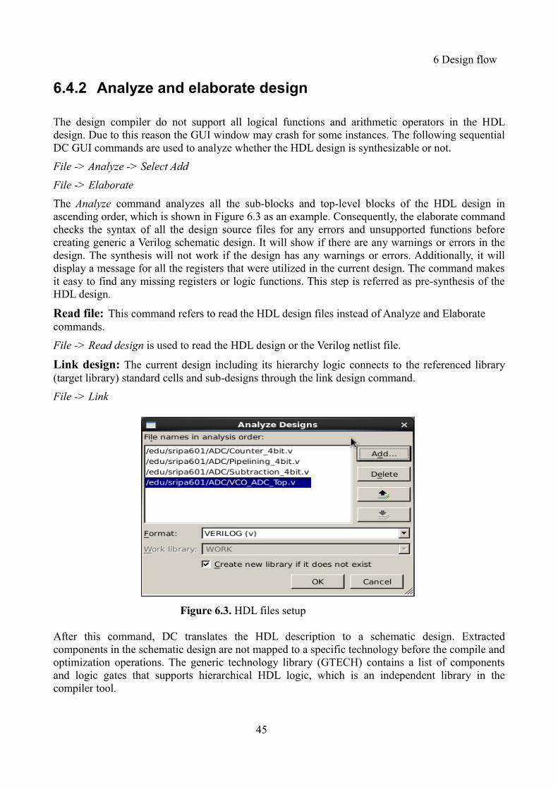
6 Design flow
6.4.2 Analyze and elaborate design
The design compiler do not support all logical functions and arithmetic operators in the HDLdesign. Due to this reason the GUI window may crash for some instances. The following sequentialDC GUI commands are used to analyze whether the HDL design is synthesizable or not.
File -> Analyze -> Select Add
File -> Elaborate
The Analyze command analyzes all the sub-blocks and top-level blocks of the HDL design inascending order, which is shown in Figure 6.3 as an example. Consequently, the elaborate commandchecks the syntax of all the design source files for any errors and unsupported functions beforecreating generic a Verilog schematic design. It will show if there are any warnings or errors in thedesign. The synthesis will not work if the design has any warnings or errors. Additionally, it willdisplay a message for all the registers that were utilized in the current design. The command makesit easy to find any missing registers or logic functions. This step is referred as pre-synthesis of theHDL design.
Read file: This command refers to read the HDL design files instead of Analyze and Elaborate commands.
File -> Read design is used to read the HDL design or the Verilog netlist file.
Link design: The current design including its hierarchy logic connects to the referenced library(target library) standard cells and sub-designs through the link design command.
File -> Link
After this command, DC translates the HDL description to a schematic design. Extractedcomponents in the schematic design are not mapped to a specific technology before the compile andoptimization operations. The generic technology library (GTECH) contains a list of componentsand logic gates that supports hierarchical HDL logic, which is an independent library in thecompiler tool.
45
Figure 6.3. HDL files setup
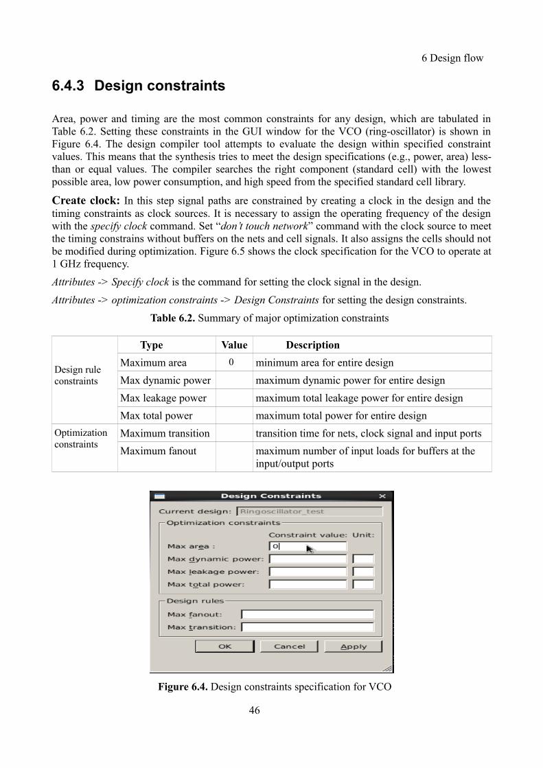
6 Design flow
6.4.3 Design constraints
Area, power and timing are the most common constraints for any design, which are tabulated inTable 6.2. Setting these constraints in the GUI window for the VCO (ring-oscillator) is shown inFigure 6.4. The design compiler tool attempts to evaluate the design within specified constraintvalues. This means that the synthesis tries to meet the design specifications (e.g., power, area) less-than or equal values. The compiler searches the right component (standard cell) with the lowestpossible area, low power consumption, and high speed from the specified standard cell library.
Create clock: In this step signal paths are constrained by creating a clock in the design and thetiming constraints as clock sources. It is necessary to assign the operating frequency of the designwith the specify clock command. Set “don’t touch network” command with the clock source to meetthe timing constrains without buffers on the nets and cell signals. It also assigns the cells should notbe modified during optimization. Figure 6.5 shows the clock specification for the VCO to operate at1 GHz frequency.
Attributes -> Specify clock is the command for setting the clock signal in the design.
Attributes -> optimization constraints -> Design Constraints for setting the design constraints.
Table 6.2. Summary of major optimization constraints
Design ruleconstraints
Type Value Description
Maximum area 0 minimum area for entire design
Max dynamic power maximum dynamic power for entire design
Max leakage power maximum total leakage power for entire design
Max total power maximum total power for entire design
Optimizationconstraints
Maximum transition transition time for nets, clock signal and input ports
Maximum fanout maximum number of input loads for buffers at the input/output ports
46
Figure 6.4. Design constraints specification for VCO

6 Design flow
6.4.4 Design environment
The design environment restrictions tell the design compiler tool in which environment (operatingconditions and system interface requirements) the circuit is expected to operate. The mainenvironment constraints include operating conditions and wire load models.
Input delay and output delay: Use the following commands to specify the certain timinginformation (e.g., propagation delay) on input and output signal paths with respect to the clocksignal in the design.
Attributes -> Operating Environment -> Input Delay
Attributes -> Operating Environment -> Output Delay
Wire load: This gives an option for the circuit designer to select the required wire load andanalyze the effects of different wire load models (resistance and capacitance variations) on thecircuit performance. Wire load models provided from technology library are shown in Figure 6.6.
Attributes -> Operating Environment -> Wire Load is the command to select the wire load for thedesign.
Operating conditions: The design could be analyzed in different operating conditions. Thecircuit performance can be determined with minimum to maximum cases in temperature, inputsupply voltage, and CMOS process variations. For example, the circuit performances with differenttemperature ranges, wire load, wc_CMOS (worst case), bc_CMOS (best case) process, and supplyvoltage range can be chosen in the design compiler. The GUI command is shown below andwindow for setting the operating conditions for the circuit is shown in Figure 6.7.
Attributes -> Operating Environment -> Operating Conditions
47
Figure 6.5. Clock signal specification

6 Design flow
Driving cell: In general, the standard cells have different setup and hold timings, so this commandadds a driving cell between sub-blocks that helps to meet these time requirements and limits thetime difference.
Attributes -> Operating Environment -> Drive cell
Loads on Input and Output ports: This command sets the load capacitance value andtransition time for input and output ports that connect to the chip pads.
Attributes -> Operating Environment -> Load
Compile: Checks the design before compiling for any multi-connected ports of input sources orany inconsistencies. The architecture can be compiled using either top-down or bottom-up or mixedcompile options. After giving the compile command, a block level schematic view of the currentdesign with specified library standard cells can be displayed using “Create Design Schematicoption”. The design check and compile commands from GUI menu are listed below.
Design -> Check
Design -> Compile
48
Figure 6.6. Selecting wire load
Figure 6.7. Setting operating conditions

6 Design flow
6.4.5 Optimize design
The optimization step in the synthesis process attempts to meet the design goals and the correctfunctionality. This process is repeated if the HDL design is not able to map the gate-level netlistaccording to circuit functionality. In general the optimization process includes the architectural(e.g., reordering operators), logic-level (e.g., structuring) and gate-level (e.g., mapping, delay)optimization. The current design optimization is performed by “Design -> Compile” command.
Design reports: The design compiler tool provides various reports after optimizing the gate-levelnetlist of the HDL design. The reports are essential to compare the various synthesis results of thedesign and to ensure the accurate design. In addition, it ensures correctness of the circuit designfunction. Some equivalent commands are shown below to analyze the design on the total area,power consumption, and circuit timing.
Design -> Report Design
Design -> Report Area
Design -> Report Power
Design -> Report Timing Paths
6.4.6 Database
More design and environmental constraints can be chosen for the synthesis process to provide theADC efficient performance and precise timing on signal paths. However, a straightforwardsynthesis procedure has been followed here to implement the functionality of the VCO-based ADC.Through this synthesis, the Verilog netlist file was generated from the Synopsys Design-Compilerthat contains information about the entire circuit schematic level design connectivity. The obtainednetlist file was imported into Cadence Virtuoso ADE for transistor level simulations and finallayout.
DDC: Synopsys internal database format is listed below,
File -> save as -> File name -> Format -> ddc or DC shell command “write -hierarchy -format ddc VCO_ADC_Top” is used to save the Synopsys GUI design format.
Verilog/VHDL (netlist):
File -> save as -> File name -> Format -> Verilog/VHDL or “write -hierarchy -format verilog -output /edu/sripa601/ADC_Top/VCO_ADC_Top_nl_6.v” is the command to write the Verilog netlist of the HDL design.
Moreover, .sdc file gives information about timing constraints (input-output delay, drive strength)for the place and route tool. The commands are listed below to write .sdc file of the design.
SDC (Synopsys Delay constraints): write_sdc -nosplit VCO_ADC_Top.sdc
SDF (standard Delay Format):write_sdf -version 2.1 VCO_ADC_Top.sdf
49
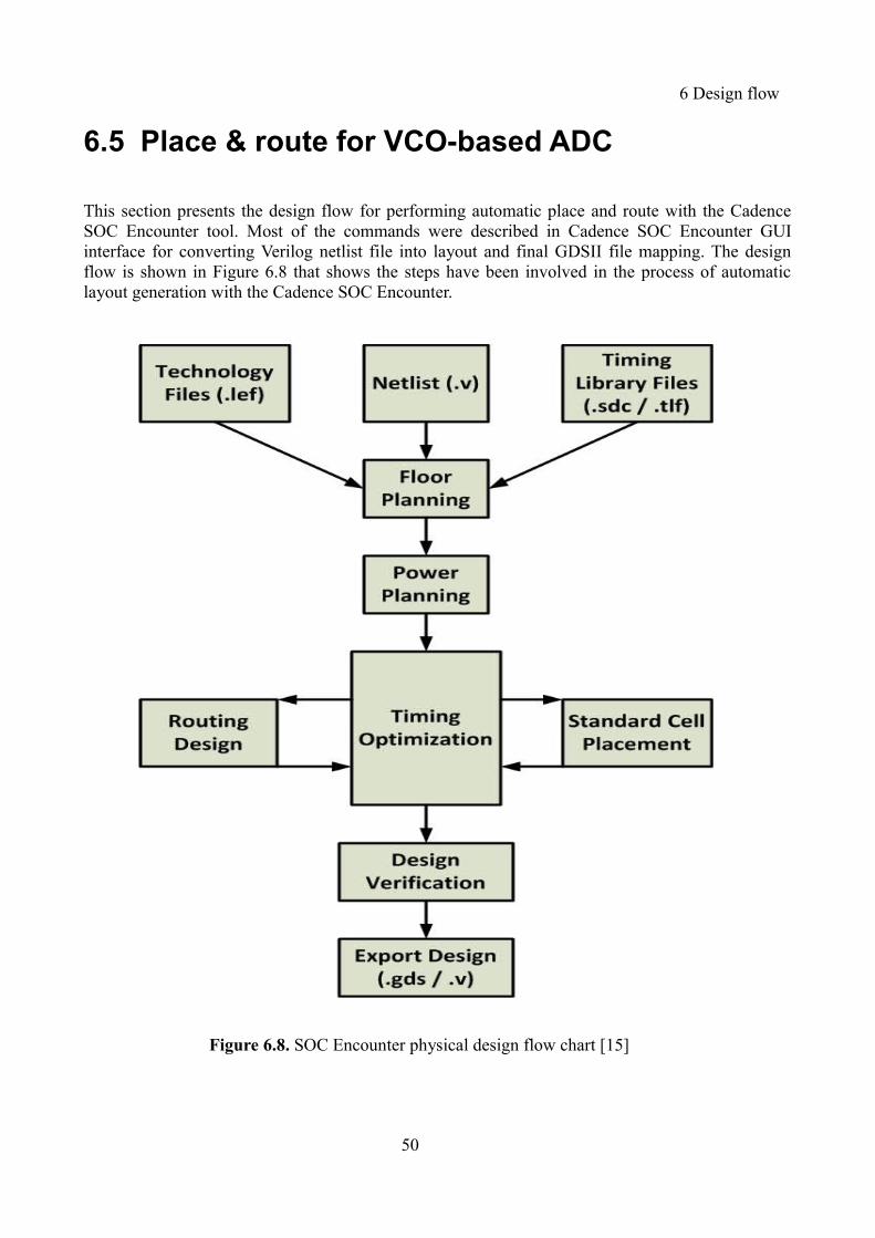
6 Design flow
6.5 Place & route for VCO-based ADC
This section presents the design flow for performing automatic place and route with the CadenceSOC Encounter tool. Most of the commands were described in Cadence SOC Encounter GUIinterface for converting Verilog netlist file into layout and final GDSII file mapping. The designflow is shown in Figure 6.8 that shows the steps have been involved in the process of automaticlayout generation with the Cadence SOC Encounter.
50
Figure 6.8. SOC Encounter physical design flow chart [15]

6 Design flow
6.5.1 Design import
Design import is the first step in the place and route process. It requires the technology database,which is listed in Table 6.3.
Table 6.3. Database to import in Encounter
Library Physical library (.lef)
Timing information library (.lib)
User data base Gate-level Verilog netlist
SDC constraints (.sdc)
IO pads, corner pads (.IO)
Importing the Verilog netlist file into the design import window needs the technology libraryexchange format files, which are summarized in Table 6.4. Instead of a .tlf file, the current designuses the minimum and maximum timing libraries for setting up timing information for the design.In general, analog blocks can have the same power supplies for both substrates and power supplyterminals. The power information (i.e., global nets-vdd, gnd) of the current design is written in theconfiguration file (.conf), which is created from the design import window after setting thetechnology files and Verilog netlist file.
File -> Import design is the GUI command to open the design import window to import the database. Save -> Config creates the configuration file (.conf) from the design import window.
Moreover, the configure file can be reloaded from the design import window to specify the powerplanning of the core. An example of the configuration file for the VCO-based ADC block isattached in the appendix.
Table 6.4. Technology files database to be imported in Encounter
LEF files Technology process cmos065_7m4x0y2z_AP_Worst.lef
Standard cells and IP blocks layouts CORE65LPSVT_soc.lef
Filler cells PRHS65_soc.lef
Timing libraries (delays)
Min-best case time analysis library CORE65LPSVT_bc_1.30V_105C.lib
Max-worst case time analysis library CORE65LPSVT_wc_1.15V_125C_10y.lib
6.5.2 Floorplan
The floorplan determines the entire core size by adjusting the aspect ratio (core height/width). It ispossible to provide chip Input-Output (IO) pads orientation. The floorplan specification for the
51

6 Design flow
current VCO-based ADC (TDC block) is shown in Figure 6.9 and the corresponding command isshown below. The core to IO Boundary is specified by 4 microns for routing global nets around thecore.
Floorplan -> Specify Floorplan
6.5.3 Power planning
The power structure is created for the ADC core through the following power planning commands.
Power -> Power Planning -> Add Ring -> Advanced:
Power -> Connect Global Nets -> vdd/gnd pin names
-> vdd Tie High to global net vdd
-> gnd Tie Low to global net gnd
Here, vdd and gnd labels are representing the inner ring and outer ring power supply of the core.
Power -> Power Planning -> Add Ring: This command is used for routing the power supply of theentire core with specified global nets in the design. Furthermore, it is necessary to set the directionsof power strips to connect IO pads of the chip and the power strip extension is shown in Figure6.10.
Power -> Power Planning -> Add Ring -> Advanced:
Power -> Power Planning -> Add Stripes: Optional power stripes in vertical and horizontaldirections across the core.
52
Figure 6.9. Floorplan specification of the ADC

6 Design flow
6.5.4 Substrate bias planning
There are two ways for power distribution to the PMOS and NMOS substrates of the standard cells.The first method is to add a Well-Tap (body-bias cell) to the standard cells in the core. The secondmethod is to use In-Cell taps that are standard cells having vddbias and vssbias pins. In addition dothe In-Cell tap standard cells not require any body-bias cells in the core. In practice, each standardcell row of the layout should have at least one body-bias cell to provide the vddbias to n-well (i.e.,PMOS bulk) and vssbias to p-sub (i.e., NMOS bulk) respectively [13]. The specified technologylibrary (STM 65 nm) provides two types of body-bias cells, which are used to connect automaticallybetween standard cells substrate and global nets such as vdd and gnd of core. These body-bias cellsare the following.
• No-split power substrate straps: same power supply is used both vdd, vddbias (PMOS bulk).
Ex. HS65_LS_FILLERNPWPFP3/4
• Split power substrate straps: separate power supply is used both vdd, vddbias (PMOS bulk).
Ex. HS65_LS_FILLERSNPWPFP3/4
As per design specification, HS65_LS_FILLERNPWPFP3/4 has filled in each standard cell row ofthe core. An example of this substrate bias planning is shown in Figure 6.11 that shows how thesecells are placed at the starting and ending point of each standard cell row of the core.
Place> Physical Cell > Add Well Tap Instances is a step to add these cells in the core.
53
Figure 6.10. Power planning around the core
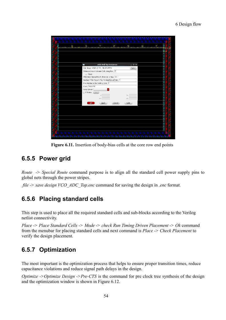
6 Design flow
6.5.5 Power grid
Route -> Special Route command purpose is to align all the standard cell power supply pins toglobal nets through the power stripes.
file -> save design VCO_ADC_Top.enc command for saving the design in .enc format.
6.5.6 Placing standard cells
This step is used to place all the required standard cells and sub-blocks according to the Verilog netlist connectivity.
Place -> Place Standard Cells -> Mode -> check Run Timing Driven Placement -> Ok command from the menubar for placing standard cells and next command is Place -> Check Placement to verify the design placement.
6.5.7 Optimization
The most important is the optimization process that helps to ensure proper transition times, reduce capacitance violations and reduce signal path delays in the design.
Optimize ->Optimize Design ->Pre-CTS is the command for pre clock tree synthesis of the designand the optimization window is shown in Figure 6.12.
54
Figure 6.11. Insertion of body-bias cells at the core row end points

6 Design flow
The critical path in the design is called worst negative slack (WNS). It is obvious that the criticalpath of the design should be a positive value. Otherwise, it shows that the design does not meet thetiming constraints. An example of the pre-optimization summary for the VCO-based ADC is shownin Table 6.5.
Table 6.5. Pre-CTS optimized summary for TDC in the VCO-based ADC
----------------------------------------------------------------------------------------------------------- optDesign Summary ----------------------------------------------------------------------------------------------------------- Setup mode all reg2reg in2reg reg2out in2out clkgate ----------------------------------------------------------------------------------------------------------- WNS (ns) 0.020 0.020 N/A N/A N/A N/A TNS (ns) 0.000 0.000 N/A N/A N/A N/A Violating Paths 0 0 N/A N/A N/A N/A All Paths 104 104 N/A N/A N/A N/A-----------------------------------------------------------------------------------------------------------Density: 95.159% Routing Overflow: 0.00% H and 0.00% V
6.5.8 Clock tree synthesis (optional)
This process is required to assign clock signal phases for the standard cells in order to minimize theskew and jitter of the clock signal in the circuit. It can also define a synchronous clock signalthrough the design. The required clock tree specification plan has to be created in .ctstch file withthe following commands. The clock tree topology in the core (TDC) is shown in Figure 6.13.
Clock-> Synthesize Clock Tree -> Gen Spec
Clock -> Display -> Display Clock
55
Figure 6.12. Pre-CTS optimization for VCO-based ADC
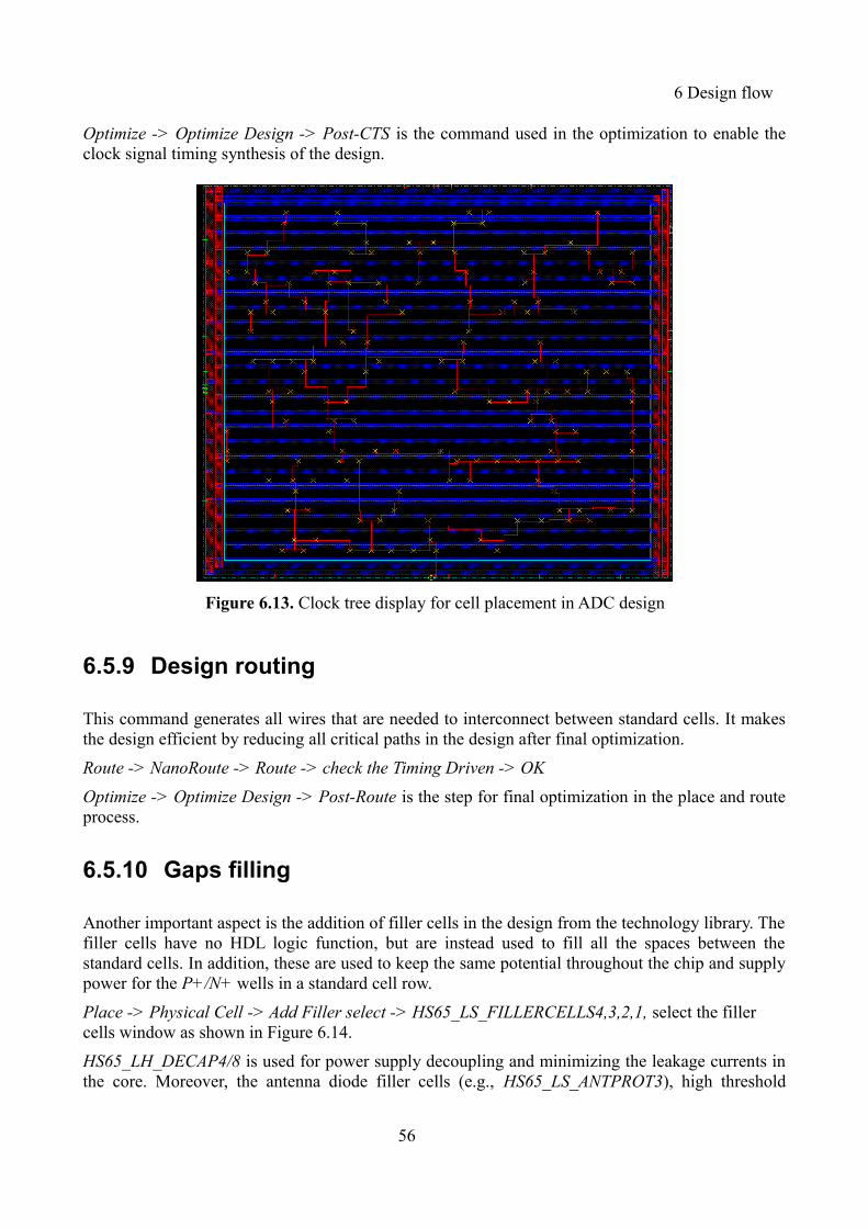
6 Design flow
Optimize -> Optimize Design -> Post-CTS is the command used in the optimization to enable theclock signal timing synthesis of the design.
6.5.9 Design routing
This command generates all wires that are needed to interconnect between standard cells. It makesthe design efficient by reducing all critical paths in the design after final optimization.
Route -> NanoRoute -> Route -> check the Timing Driven -> OK
Optimize -> Optimize Design -> Post-Route is the step for final optimization in the place and routeprocess.
6.5.10 Gaps filling
Another important aspect is the addition of filler cells in the design from the technology library. Thefiller cells have no HDL logic function, but are instead used to fill all the spaces between thestandard cells. In addition, these are used to keep the same potential throughout the chip and supplypower for the P+/N+ wells in a standard cell row.
Place -> Physical Cell -> Add Filler select -> HS65_LS_FILLERCELLS4,3,2,1, select the filler cells window as shown in Figure 6.14.
HS65_LH_DECAP4/8 is used for power supply decoupling and minimizing the leakage currents inthe core. Moreover, the antenna diode filler cells (e.g., HS65_LS_ANTPROT3), high threshold
56
Figure 6.13. Clock tree display for cell placement in ADC design

6 Design flow
voltage supply decoupling cells (e.g., HS65_LH_DECAP4), filler cells with pattern fill for PO (e.g.,HS65_LH/LL/LS/GH/GS/GL_FILLERPFOP8), and the oxide diffusion well-straps standard cells(e.g., HS65_LH/LL/LS_FILLERNPW3/4) are used in the core to avoid potential issues and leakagecurrents.
6.5.11 Design checks
Design check step verifies the entire layout to not contain any antenna errors or connectivity errors.The Cadence SOC Encounter provides various reports for analyzing the timing information onsignal paths. The layout can be verified by using the following commands from the GUI mainmenu.
Check DRC
Verify -> Verify Geometry
Verify -> Verify Connectivity
6.5.12 Export files
A layer mapping file is required while generating GDSII file of the design. The layer mapping tellsthe Cadence software that the layout in the .gds file is mapped to a specific technology.
The layer mapping file from the technology directory is named cmos065_7m4x0y2z_AP.mapOut.
57
Figure 6.14. Specification of the core filler cells in the ADC

6 Design flow
File -> Save -> GDS/OASIS is the command for writing .gds file and the GUI window as shown inFigure 6.15. A useful command in the console in SOC Encounter that streams out the gds file isshown below.
streamOut VCO_ADC_Counter.gds -mapFile/sw/cadence/libraries/cmos065RF_534_IC615.010/[email protected]/TECH/cmos065_7m4x0y2z_AP.mapOut-libNameDesignLib-outputMacros-dieAreaAsBoundary -units 1000 -mode ALL
6.6 Design import in Cadence Virtuoso
The VCO and the rest of the ADC layouts were generated from Cadence SOC Encounter and afterthat individual GDSII files were imported in Cadence Virtuoso for generating the final layout of theVCO-based ADC and subsequently netlists for post layout simulations. During streaming ofthe .gds file, a template file can be created to provide the mapping information between metal layersin the .gds file and the technology library in the Cadence ADE. As an example there is a templatefile attached in the appendix, which shows the required layer mapping files (e.g.,cmos065.layermap, cmos065.objectmap) from the technology directory.
6.6.1 Layout area
The final layout area of the VCO is 7×14 μ m2 and the rest of the ADC block is 73×77 μ m2 .The layout of the TDC quantizer is shown in Figure 6.16.
58
Figure 6.15. gds file streaming

6 Design flow
6.6.2 Design verification in Calibre
Mentor Graphics Calibre tool is used for DRC, LVS, and ERC verification of the VCO-based ADClayout. In this verification flow, the Calibre LVS verification step requires a black box statement ofevery standard cell of the design from the technology library. The black box statement can bewritten as LVS BOX cell_name in the Standard-Verification-Rule-Format (SVRF) tab. This stepchecks the connectivity between standard cells in the layout versus schematic of the design. TheCalibre LVS run command is shown below and the corresponding window is shown in Figure 6.17.
LVS Options -> include -> Include SVRF Commands-> LVS BOX HS65_LS_IVX9
59
Figure 6.16. Layout of the implemented TDC
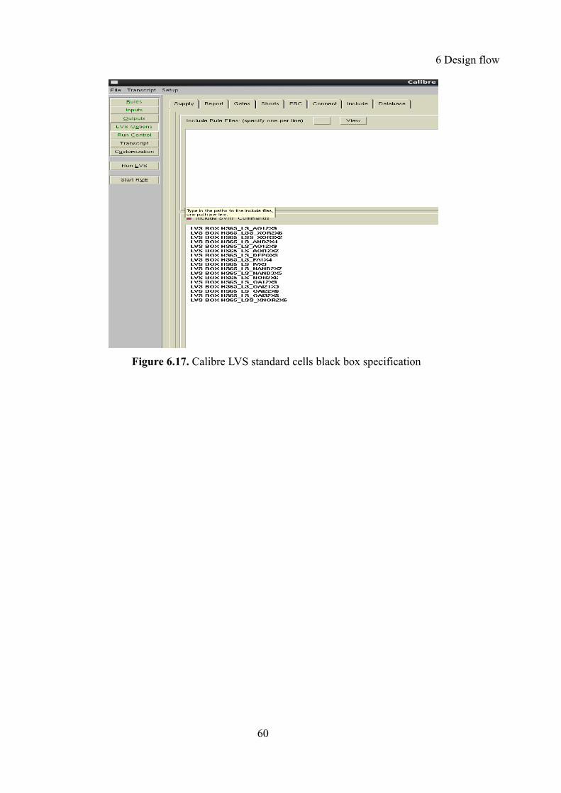
6 Design flow
60
Figure 6.17. Calibre LVS standard cells black box specification

7 Conclusion
7 Conclusion
The VCO-based ADC design was implemented using a complete RTL-GDSII design flow based ondigital EDA tools such as Synopsys Design Compiler and Cadence SOC Encounter. A simple HDLlogic and fully digital implementation of a VCO-based ADC offers shorter design time and reducesthe design cost. Moreover, the time-domain signal processing of an all-digital ADC allows superiortime resolution, low power consumption, and low silicon area in a deep submicron CMOS process.The thesis work dealt with understanding ideal VCO-based ADC theory and the effects ofnonidealities such as VCO non-linearity, sampling clock jitter, flip-flop metastability, and VCOdelay cell mismatches on the performance of the circuit. In this project, a single ended 13-stagering-oscillator is used as a multi-phase VCO that together with a 13-stage 4-bit quantizationarchitecture (QSD) has been implemented. The functional verification has been done in the CadenceVirtuoso simulator. The resulting circuit shows flip-flop metastability problems at high samplingrates. For instance, circuit simulation at 500 MHz sampling frequency produces spikes in the digitaloutput signal. These spikes in the digital signal are limiting the noise-shaping property. Thedynamic performance of the designed VCO-based ADC circuit is analyzed at the 100 MHzsampling frequency. The implemented architecture delivers an SNR that is 30 dB, SNDR is 25.4dB, ENOB is 3.92, and THD is -27.66 dB for a 0.5 Vp-p and 4.98 MHz sinusoidal input signal. Theaverage power consumption of the total schematic circuit is 630 μW. In the future, technologyscaling together with all-digital ADC design should be able to deliver competitive performancecompared with conventional analog ADC design.
7.1 Future work
Proposed future work to this thesis can be divided into two categories. The first is based on digitalsignal processing and the second is based on fabrication point of view.
• As noted previously in Chapter 1, the digital post processing is a part of VCO-based ADCdesign that will be carried out as future work.
• The designed VCO-based ADC is verified with circuit level simulations. The dynamicperformance is analyzed with respect to overall circuit performance at a high frequencyinput signal. In contrast, the static analysis provides the ADC characteristics by applying aslow ramp signal. This infers a difference between ideal and measured transfer function thatestimates the compensation codes. This is left as a future task.
• Future tasks may also involve the post layout simulation and comparison with schematicsimulations.
• A future task may also include the final layout with I/O pads, ESD protection, IR dropanalysis, and final GDSII file for fabrication.
• The digital differential ring-oscillator as a VCO has to be designed and verified with multi-bit quantization architecture for high linearity over a full scale input voltage.
61

7 Conclusion
• There are several pseudo-differential VCO-ADC architectures that can be implemented witha RTL-GDSII design flow. For example, pseudo-differential VCO-ADC with digitalcalibration [5].
• The possibility of reducing the flip-flop metastability problems in the implemented VCO-based ADC could be investigated.
62

Appendix
• TCL script for VCO
gui_startanalyze -format verilog {/edu/sripa601/ADC/Ringoscillator_1.v} elaborate Ringoscillator_test_13 -architecture verilog -library WORK -update link uniquify -forcecreate_clock -name "clk" -period 1 -waveform { 0 0.5 } set_dont_touch_network [ find clock clk ] set_max_area 0set_operating_conditions -library CORE65LPSVT bc_1.30V_105C set_wire_load_model -name area_0Kto1K -library CORE65LPSVTset_disable_timing I_0 set_disable_timing I_1 set_disable_timing I_2 set_disable_timing I_3 set_disable_timing I_4 set_disable_timing I_5 set_disable_timing I_6 set_disable_timing I_7 set_disable_timing I_8 set_disable_timing I_9 set_disable_timing I_10 set_disable_timing I_11 set_disable_timing I_12set_ungroup Ringoscillator_test_13 set_dont_touch Ringoscillator_test_13 set_boundary_optimization Ringoscillator_test_13 compile_ultra -exact_map -no_seq_output_inversionuplevel #0 { report_cell } uplevel #0 { report_design } uplevel #0 { report_hierarchy } uplevel #0 { report_port } uplevel #0 { report_cell } uplevel #0 { report_area -nosplit } uplevel #0 { report_power -analysis_effort low } uplevel #0 { report_resources } uplevel #0 { report_wire_load -design Ringoscillator_test_13 }uplevel #0 { report_constraint -all_violators -significant_digits 2 -max_area -max_delay -critical_range -min_delay -max_capacitance-min_capacitance -max_transition -max_fanout -cell_degradation -max_dynamic_power -max_leakage_power -connection_class -multiport_net }
63
write -hierarchy -format ddcwrite -hierarchy -format verilog -output /edu/sripa601/ADC_Top/VCO_ADC_TOP_VCO_nl.v write -hierarchy -format ddc -output /edu/sripa601/ADC_Top/VCO_ADC_TOP_VCO_ddc.ddc write_sdf -version 2.1 VCO_ADC_VCO.sdf write_sdc -nosplit VCO_ADC_VCO.sdc
• Configuration File
############################################################### # Generated by: Cadence Encounter 10.10-p003_1 # OS: Linux x86_64(Host ID sob-10.edu.isy.liu.se) # Generated on: Wed Jan 22 20:38:49 2014 # Design: VCO_ADC_Top # Command: saveDesign VCO_ADC_Top_1.enc ############################################################### global rda_Input set cwd /edu/sripa601/socencounter set rda_Input(import_mode) {-treatUndefinedCellAsBbox 0 -keepEmptyModule 1 } set rda_Input(ui_netlist) "VCO_ADC_Top_1.enc.dat/VCO_ADC_Top.v.gz"set rda_Input(ui_netlisttype) {Verilog} set rda_Input(ui_rtllist) "" set rda_Input(ui_ilmdir) "" set rda_Input(ui_ilmlist) "" set rda_Input(ui_ilmspef) "" set rda_Input(ui_fmdir) {} set rda_Input(ui_settop) {1} set rda_Input(ui_topcell) {VCO_ADC_Top} set rda_Input(ui_celllib) "" set rda_Input(ui_iolib) "" set rda_Input(ui_areaiolib) "" set rda_Input(ui_blklib) "" set rda_Input(ui_kboxlib) "" set rda_Input(ui_gds_file) "" set rda_Input(ui_oa_oa2lefversion) {} set rda_Input(ui_view_definition_file) "" set rda_Input(ui_timelib,max) "/sw/cadence/libraries/cmos065RF_534_IC615.010/CORE65LPSVT_5.1/libs/CORE65LPSVT_wc_1.15V_125C_10y.lib" set rda_Input(ui_timelib,min) "/sw/cadence/libraries/cmos065RF_534_IC615.010/CORE65LPSVT_5.1/libs/CORE65LPSVT_bc_1.30V_105C.lib" set rda_Input(ui_timelib) "" set rda_Input(ui_smodDef) "" set rda_Input(ui_smodData) "" set rda_Input(ui_locvlib) ""
64

set rda_Input(ui_dpath) "" set rda_Input(ui_tech_file) "" set rda_Input(ui_io_file) "" set rda_Input(ui_timingcon_file,full) "" set rda_Input(ui_timingcon_file) "" set rda_Input(ui_latency_file) "" set rda_Input(ui_scheduling_file) "" set rda_Input(ui_buf_footprint) {} set rda_Input(ui_delay_footprint) {} set rda_Input(ui_inv_footprint) {} set rda_Input(ui_leffile) "/sw/cadence/libraries/cmos065RF_534_IC615.010/[email protected]/TECH/cmos065_7m4x0y2z_AP_Worst.lef /sw/cadence/libraries/cmos065RF_534_IC615.010/CORE65LPSVT_5.1/CADENCE/LEF/CORE65LPSVT_soc.lef /sw/cadence/libraries/cmos065RF_534_IC615.010/PRHS65_7.0.a/CADENCE/LEF/PRHS65_soc.lef" set rda_Input(ui_cts_cell_footprint) {} set rda_Input(ui_cts_cell_list) {} set rda_Input(ui_core_cntl) {aspect} set rda_Input(ui_aspect_ratio) {1.0} set rda_Input(ui_core_util) {0.7} set rda_Input(ui_core_height) {65.0} set rda_Input(ui_core_width) {69.225} set rda_Input(ui_core_to_left) {4.0} set rda_Input(ui_core_to_right) {4.0} set rda_Input(ui_core_to_top) {4.0} set rda_Input(ui_core_to_bottom) {4.0} set rda_Input(ui_max_io_height) {0} set rda_Input(ui_row_height) {2.6} set rda_Input(ui_isHorTrackHalfPitch) {0} set rda_Input(ui_isVerTrackHalfPitch) {1} set rda_Input(ui_ioOri) {R0} set rda_Input(ui_isOrigCenter) {0} set rda_Input(ui_isVerticalRow) {0} set rda_Input(ui_exc_net) "" set rda_Input(ui_delay_limit) {1000} set rda_Input(ui_net_delay) {1000.0ps} set rda_Input(ui_net_load) {0.5pf} set rda_Input(ui_in_tran_delay) {0.1ps} set rda_Input(ui_captbl_file) "" set rda_Input(ui_preRoute_cap) {1} set rda_Input(ui_postRoute_cap) {1} set rda_Input(ui_postRoute_xcap) {1} set rda_Input(ui_preRoute_res) {1} set rda_Input(ui_postRoute_res) {1} set rda_Input(ui_shr_scale) {1.0} set rda_Input(ui_rel_c_thresh) {0.03} set rda_Input(ui_tot_c_thresh) {5.0}
65
set rda_Input(ui_cpl_c_thresh) {3.0} set rda_Input(ui_time_unit) {none} set rda_Input(ui_cap_unit) {} set rda_Input(ui_oa_reflib) {} set rda_Input(ui_oa_abstractname) {} set rda_Input(ui_oa_layoutname) {} set rda_Input(ui_sigstormlib) "" set rda_Input(ui_cdb_file,min) "" set rda_Input(ui_cdb_file,max) "" set rda_Input(ui_cdb_file) "" set rda_Input(ui_xtwf_file) "" set rda_Input(ui_qxtech_file) "" set rda_Input(ui_qxlayermap_file) "" set rda_Input(ui_qxlib_file) "" set rda_Input(ui_qxconf_file) "" set rda_Input(ui_pwrnet) {vdd } set rda_Input(ui_gndnet) {gnd } set rda_Input(flip_first) {1} set rda_Input(double_back) {1} set rda_Input(assign_buffer) {1} set rda_Input(use_io_row_flow) {0} set rda_Input(ui_pg_connections) "" set rda_Input(ui_gen_footprint) {0}
• Template_to_Import_gds_In_Cadence
#dbuPerUU "0" #hierDepth "32767" #maxCellsInTargetLib "20000" #numThreads "1" #strmTextNS "cdba" #arrayInstToScalar attachTechFileOfLib "" case "preserve" cellMap "" #checkPolygon #convertPathToPathSeg #detectVias #disableLocking excludeMapToVia "" fontMap "" #ignoreBoxes #ignoreZeroWidthPath #keepStreamCells labelCase "preserve" layerMap"/edu/sripa601/digRf/../../../sw/cadence/libraries/cmos065RF_534_I
66
C615.010/[email protected]/DATA/LIB/lib/OpenAccess/cmos065/cmos065.layermap" library "vco2" loadTechFile "" logFile "strmIn.log" #mergeUndefPurposToDrawing noInfo "" #noOverwriteCell noWarn "" objectMap"/edu/sripa601/digRf/../../../sw/cadence/libraries/cmos065RF_534_IC615.010/[email protected]/DATA/LIB/lib/OpenAccess/cmos065/cmos065.objectmap" pinAttNum "0" propMap "" propSeparator "," refLibList "CORE65LPSVT" #replaceBusBitChar #reportPrecisionLoss runDir"/edu/sripa601/digRf/work_sripa601/log" scaleTextHeight "1.00000" #skipUndefinedLPP #snapToGrid strmFile"/edu/sripa601/socencounter/ADC_fs_1.gds" strmTechGen "" summaryFile "" techRefs "CORE65LPSVT" topCell "" #translateNode userSkillFile "" viaMap "" view "layout" warnToErr ""
67

References [1] Georges Gielen, Wim Dehaene , “Analog and digital circuit design in 65 nm CMOS: end of the
road?”, ESAT-MICAS, URL: http://arxiv.org/pdf/0710.4709.pdf?origin=publication_detail
[2] Vishnu Unnikrishnan, “Design of a VCO-based all-digital ADC”, Student thesis,ISRN: LiTH-ISY-EX--12/4546--SE, Electronics systems 2012, Linköping University,
[3] Walt Kester, Dan Sheingold, “TESTING DATA CONVERTERS, CHAPTER 5”, URL:http://www.analog.com/library/analogdialogue/archives/39-06/Chapter%205%20Testing%20Converters%20F.pdf
[4] Kent H. Lundberg “Analog-to-Digital Converter Testing”, 2002, URL: http://web.mit.edu/klund/www/papers/UNP_A2Dtest.pdf
[5] Jorg Daniels, Wim Dehaene, Michiel Steyaert, “All-Digital Differential VCO-based A/DConversion”, Circuits and Systems (ISCAS), IEEE International Symposium on, Page(s): 1085– 1088, May 30 2010.
[6] Behzad Razavi, “Design of Analog CMOS Integrated Circuits”, McGraw-Hill series, Electrical and Computer engineering.
[7] Bergs Joakim, “Design of a VCO based ADC in a 180 nm CMOS process for use in positronemission tomography”, Student thesis, Systemteknik / EISLAB, LTU, Sweden, 2010. URL:http://epubl.ltu.se/1402-1617/2010/069/
[8] Jaewook Kim, Tae-Kwang Jang, Young-Gyu Yoon, SeongHwan Cho, “Analysis and Design ofVoltage-Controlled Oscillator Based Analog-to-Digital Converter”, Circuits and Systems I:Regular Papers, IEEE Transactions on, Page(s): 18-30, Jan. 2010.
[9] Jaewook Kim, Seonghwan Cho, “A Time-Based Analog-to-Digital Converter Using a Multi-Phase Voltage-Controlled Oscillator”, Circuits and Systems, IEEE International Symposium on,Page(s): 4 pp. - 3937, May 2006.
[10] Synopsys, “Design Compiler User Guide Version D-2010.03-SP2, June 2010”, URL: http://acms.ucsd.edu/_files/dcug.pdf
[11] Design Vision Tutorial, ECE 551, Staff Dept of Electrical & Computer Engineering, UW-Madison, URL: http://coefs.uncc.edu/amukherj/files/2012/04/DesignVisionTutorial_f07.pdf
[12] Physical Placement with Cadence SoCEncounter 7.1, URL: http:/www.eit.lth.se/fileadmin/eit/courses/etin01/manual_etc/SEtraining2.pdf
[13] A Practical Guide to Low-Power Design User Experience with CPF sec 1, URL: www.si2.org/.../PowerForward/LowPowerGuide09232009/.../lpg_sect1_...
[14] Calibre DRC/LVS verification, URL: http://asic.ams.com/hitkit/hk410/calibre_verification_flow/calibre_verification.html
[15] Ali Shah Syed Asmat, Qazi Sohaib Ayaz, “Design of an all-digital, reconfigurable sigma-delta modulator”, Student thesis, Electronics Systems, 2012. URL: http://liu.diva-portal.org/smash/record.jsf?searchId=1&pid=diva2:548758
68

Bibliography [1] Vratislav Michal “On the Low-power Design, Stability Improvement and Frequency Estimation of the CMOS Ring Oscillator”, URL: http://www.postreh.com/vmichal/papers/Stability-CMOS-ring-oscillator.pdf
[2] Jan M. Rabaey, Anantha Chandrakasan, Borivoje Nikolic, “Digital Integrated Circuits”, 2nd Edition, Prentice Hall, January 2003.
[3] Young-Gyu Yoon, Aewook Kim, Tae-Kwang Jang, SeongHwan Cho, “A Time-Based Bandpass ADC Using Time-Interleaved Voltage-Controlled Oscillators”, IEEE Transactions on Circuits and Systems-I: Regular papers, VOL. 55, NO. 11, December 2008.
[4] Nicholas Gray, “ABCs of ADCs Analog-to-Digital Converter Basics”, National Semiconductor 2006. URL: http://www.unirioja.es/cu/lzorzano/ABCs_of_ADCs.pdf
69
Linköping University Electronic Press
Upphovsrätt
Detta dokument hålls tillgängligt på Internet – eller dess framtida ersättare –frånpubliceringsdatum under förutsättning att inga extraordinära omständigheter uppstår.
Tillgång till dokumentet innebär tillstånd för var och en att läsa, ladda ner, skrivaut enstaka kopior för enskilt bruk och att använda det oförändrat för ickekommersiellforskning och för undervisning. Överföring av upphovsrätten vid en senare tidpunktkan inte upphäva detta tillstånd. All annan användning av dokumentet kräverupphovsmannens medgivande. För att garantera äktheten, säkerheten ochtillgängligheten finns lösningar av teknisk och administrativ art.
Upphovsmannens ideella rätt innefattar rätt att bli nämnd som upphovsman i denomfattning som god sed kräver vid användning av dokumentet på ovan beskrivna sättsamt skydd mot att dokumentet ändras eller presenteras i sådan form eller i sådantsammanhang som är kränkande för upphovsmannens litterära eller konstnärligaanseende eller egenart.
För ytterligare information om Linköping University Electronic Press se förlagetshemsida http://www.ep.liu.se/
Copyright
The publishers will keep this document online on the Internet – or its possiblereplacement –from the date of publication barring exceptional circumstances.
The online availability of the document implies permanent permission for anyoneto read, to download, or to print out single copies for his/hers own use and to use itunchanged for non-commercial research and educational purpose. Subsequenttransfers of copyright cannot revoke this permission. All other uses of the documentare conditional upon the consent of the copyright owner. The publisher has takentechnical and administrative measures to assure authenticity, security andaccessibility.
According to intellectual property law the author has the right to be mentionedwhen his/her work is accessed as described above and to be protected againstinfringement.
For additional information about the Linköping University Electronic Press and itsprocedures for publication and for assurance of document integrity, please refer to itswww home page: http://w w w.ep.liu.se/ .
© Srinivasarao Pathapti