institutionen för systemteknik - diva...
TRANSCRIPT

Institutionen för systemteknikDepartment of Electrical Engineering
Examensarbete
Design of an all-digital, reconfigurable sigma-deltamodulator
Examensarbete utfört i Elektroniksystemvid Tekniska högskolan vid Linköpings universitet
av
Sohaib A. Qazi and S. Asmat Ali Shah
Linköping 2012
Department of Electrical Engineering Linköpings tekniska högskolaLinköpings universitet Linköpings universitetSE-581 83 Linköping, Sweden 581 83 Linköping
LiTH-ISY-EX--12/4557--SE


Design of an all-digital, reconfigurable sigma-deltamodulator
Examensarbete utfört i Elektroniksystemvid Tekniska högskolan vid Linköpings universitet
av
Sohaib A. Qazi and S. Asmat Ali Shah
LiTH-ISY-EX- -12/4557- -SE
Handledare: Nadeem Afzalisy, Linköpings universitet
Examinator: Dr. J. Jacob Wiknerisy, Linköpings universitet
Linköping, 17 maj 2012


Avdelning, InstitutionDivision, Department
Avdelningen för ElektroniksystemDepartment of Electrical EngineeringSE-581 83 Linköping
DatumDate
2012-05-17
SpråkLanguage
Svenska/Swedish
Engelska/English
RapporttypReport category
Licentiatavhandling
Examensarbete
C-uppsats
D-uppsats
Övrig rapport
URL för elektronisk version
http://urn.kb.se/resolve?urn=urn:nbn:se:liu:diva-XXXXX
ISBN
—
ISRN
LiTH-ISY-EX- -12/4557- -SE
Serietitel och serienummerTitle of series, numbering
ISSN
—
TitelTitle Design of an all-digital, reconfigurable sigma-delta modulator
FörfattareAuthor
Sohaib A. Qazi and S. Asmat Ali Shah
SammanfattningAbstract
This thesis presents a model of reconfigurable sigma-delta modulator. These modulators areintended for high speed digital Digital to Analog Converters. The modulators are intendedto reduce complexity of current steering DACs and also considered as a front end of dataconverters. Quantization noise present in digital signal is pushed to higher frequencies bysigma-delta modulators. Noise in high band frequencies can be removed by a low pass filter.
A test methodology involving generation of baseband signal, interpolation and digitizationis opted. Topologies tested in MATLAB® include signal feedback and error feedback modelsof first-order and second-order sigma-delta modulators. Error feedback and signal feedbackfirst-order modulators’ performance is quite similar. The SNR of a first-order error feedbackmodel is 52.3 dB and 55.9 dB for 1 and 2 quantization bits, respectively. In second-orderSDM, signal feedback provides best performance with 80 dB SNR.
The other part of the thesis focuses on the implementation of the sigma-delta modulator(SDM) using faster time to market approach. SoC Encounter, a tool from Cadence, is theeasiest way to do this job. The modulators are implemented in 65-nm technology. The re-configurable sigma-delta modulator is designed using Verilog-HDL language. Switches areintroduced to control the reconfigurable SDM for different input word lengths. Word-lengthcan vary from 0 to 4 bits. Modulator is designed to work for frequencies of 2 GHz. To netlistthe design, Design Compiler is used which is a tool from Synopsys®.
The area of the chip reported by design compiler is 563.68 um. When the design is imple-mented in SoC Encounter, area of the chip is increased, because the core utilization, whiledesigning, is only 60%, which is 556.8 um. Remaining 40% area is used by buffers, inverterand filler cells during clock tree synthesis. The buffers and inverters are added to removethe clock phase delay between different registers. Power consumption of the chip is 319 mW.Internal power of the modulators is 219.1 mW. Switching power of output capacitances is99.9 mW, which is 31% of the total power consumed. Main concern of the power loss isconsidered to be power leakage. To reduce the leakage power and achieve high speed de-sign CORE65GPHVT libraries are used. Leakage power of the design is 2.825 uW which is0.00088% of the total power.
NyckelordKeywords problem, lösning

Abstract
This thesis presents a model of reconfigurable sigma-delta modulator. Thesemodulators are intended for high speed digital Digital to Analog Converters. Themodulators are intended to reduce complexity of current steering DACs and alsoconsidered as a front end of data converters. Quantization noise present in dig-ital signal is pushed to higher frequencies by sigma-delta modulators. Noise inhigh band frequencies can be removed by a low pass filter.
A test methodology involving generation of baseband signal, interpolation anddigitization is opted. Topologies tested in MATLAB® include signal feedback anderror feedback models of first-order and second-order sigma-delta modulators.Error feedback and signal feedback first-order modulators’ performance is quitesimilar. The SNR of a first-order error feedback model is 52.3 dB and 55.9 dBfor 1 and 2 quantization bits, respectively. In second-order SDM, signal feedbackprovides best performance with 80 dB SNR.
The other part of the thesis focuses on the implementation of the sigma-deltamodulator (SDM) using faster time to market approach. SoC Encounter, a toolfrom Cadence, is the easiest way to do this job. The modulators are implementedin 65-nm technology. The reconfigurable sigma-delta modulator is designed us-ing Verilog-HDL language. Switches are introduced to control the reconfigurableSDM for different input word lengths. Word-length can vary from 0 to 4 bits.Modulator is designed to work for frequencies of 2 GHz. To netlist the design,Design Compiler is used which is a tool from Synopsys®.
The area of the chip reported by design compiler is 563.68 um. When the designis implemented in SoC Encounter, area of the chip is increased, because the coreutilization, while designing, is only 60%, which is 556.8 um. Remaining 40%area is used by buffers, inverter and filler cells during clock tree synthesis. Thebuffers and inverters are added to remove the clock phase delay between differ-ent registers. Power consumption of the chip is 319 mW. Internal power of themodulators is 219.1 mW. Switching power of output capacitances is 99.9 mW,which is 31% of the total power consumed. Main concern of the power loss isconsidered to be power leakage. To reduce the leakage power and achieve highspeed design CORE65GPHVT libraries are used. Leakage power of the design is2.825 uW which is 0.00088% of the total power.
iii


Acknowledgments
First of all, all the praise and gratitude is for Allah SWT, who gave us strengthand courage to complete this thesis in time.
We would like to thank our supervisor Mr. Nadeem Afzal who helped us throughout our thesis work. A special thanks to our examiner Dr. J. Jacob Wikner forhis kind support throughout our thesis. Mr J. Jacob Wikner’s several years ofexperience helped us to gain hands-on experience on different tools. The formatof meetings was really very helpful to judge the progress of the thesis work. Wealso thank our seniors for their kind support throughout this thesis.
We like to say thanks to our friends Muaz-un-Nabi, Shehryar Khan, Abdul Ma-teen Malik, Muhammad Suleman Khan and Muhammad Touqeer Pasha for proof-reading our report. At the end thanks to our family especially our parents, with-out their prayers and support this would not even happen.
Linköping, May 2012Sohaib A. Qazi and S. Asmat Ali Shah
v


Contents
List of Figures ix
List of Tables xii
Notation xv
I Background
1 Introduction 3
II Sigma Delta Modulators
2 Sigma Delta Modulators 92.1 Introduction . . . . . . . . . . . . . . . . . . . . . . . . . . . . . . . 92.2 Signal Feedback Sigma Delta Modulators . . . . . . . . . . . . . . . 10
2.2.1 Accumulator . . . . . . . . . . . . . . . . . . . . . . . . . . . 112.2.2 Quantizer . . . . . . . . . . . . . . . . . . . . . . . . . . . . 122.2.3 Feedback Loop . . . . . . . . . . . . . . . . . . . . . . . . . . 12
2.3 Error Feedback Sigma Delta Modulators . . . . . . . . . . . . . . . 142.4 Second-Order Signal Feedback Model . . . . . . . . . . . . . . . . . 152.5 Conclusion . . . . . . . . . . . . . . . . . . . . . . . . . . . . . . . . 16
III Processing Model for SDM
3 Processing Model for SDM 193.1 Introduction . . . . . . . . . . . . . . . . . . . . . . . . . . . . . . . 193.2 Signal Generation . . . . . . . . . . . . . . . . . . . . . . . . . . . . 193.3 Interpolation . . . . . . . . . . . . . . . . . . . . . . . . . . . . . . . 20
3.3.1 Sampling . . . . . . . . . . . . . . . . . . . . . . . . . . . . . 203.3.2 Digitization . . . . . . . . . . . . . . . . . . . . . . . . . . . 24
3.4 Conclusion . . . . . . . . . . . . . . . . . . . . . . . . . . . . . . . . 25
vii

viii CONTENTS
IV Digital Modelling of SDM
4 Digital Modeling of SDM 294.1 Introduction . . . . . . . . . . . . . . . . . . . . . . . . . . . . . . . 294.2 SoC Encounter Design Flow . . . . . . . . . . . . . . . . . . . . . . 294.3 Design Libraries . . . . . . . . . . . . . . . . . . . . . . . . . . . . . 314.4 Top Model of Sigma Delta Modulator . . . . . . . . . . . . . . . . . 324.5 Design of Re-Configurable Digital Sigma Delta Modulator . . . . . 33
4.5.1 Subtractor Module . . . . . . . . . . . . . . . . . . . . . . . 344.5.2 Delay Stage . . . . . . . . . . . . . . . . . . . . . . . . . . . 344.5.3 Integrators for Stage0 . . . . . . . . . . . . . . . . . . . . . . 344.5.4 Extension of Stage0 for Re-Configurability . . . . . . . . . . 364.5.5 Pipelining for Higher Number of Bits . . . . . . . . . . . . 38
4.6 Modeling Language for SDM . . . . . . . . . . . . . . . . . . . . . . 384.7 Test Methodology for Simulations . . . . . . . . . . . . . . . . . . . 404.8 Testbench for Simulations . . . . . . . . . . . . . . . . . . . . . . . 40
4.8.1 MATLAB Environment . . . . . . . . . . . . . . . . . . . . . 424.8.2 Interfaces . . . . . . . . . . . . . . . . . . . . . . . . . . . . . 424.8.3 Cadence Environment . . . . . . . . . . . . . . . . . . . . . 43
4.9 Conclusion . . . . . . . . . . . . . . . . . . . . . . . . . . . . . . . . 44
V Simulation Results
5 Simulation Results 475.1 Introduction . . . . . . . . . . . . . . . . . . . . . . . . . . . . . . . 475.2 Baseband Signal Generator . . . . . . . . . . . . . . . . . . . . . . . 475.3 Interpolation . . . . . . . . . . . . . . . . . . . . . . . . . . . . . . . 475.4 Filtering . . . . . . . . . . . . . . . . . . . . . . . . . . . . . . . . . 495.5 Digitization . . . . . . . . . . . . . . . . . . . . . . . . . . . . . . . . 495.6 Sigma Delta Modulators . . . . . . . . . . . . . . . . . . . . . . . . 50
5.6.1 First-Order Signal Feedback Model . . . . . . . . . . . . . . 525.6.2 First-Order Error Feedback Model . . . . . . . . . . . . . . 535.6.3 Second-Order Signal Feedback Model . . . . . . . . . . . . 545.6.4 Second-Order Error Feedback Model . . . . . . . . . . . . . 555.6.5 Comparison of Modulators . . . . . . . . . . . . . . . . . . . 55
5.7 Hardware Implementation Results . . . . . . . . . . . . . . . . . . 575.7.1 Area Consumed . . . . . . . . . . . . . . . . . . . . . . . . . 575.7.2 Power Utilization . . . . . . . . . . . . . . . . . . . . . . . . 59
5.8 Conclusion . . . . . . . . . . . . . . . . . . . . . . . . . . . . . . . . 59
VI SoC Encounter Manual
6 SoC Encounter Manual 636.1 Introduction . . . . . . . . . . . . . . . . . . . . . . . . . . . . . . . 636.2 Behavioral Modeling (MODELSIM) . . . . . . . . . . . . . . . . . . 63

6.3 Synthesis and Netlist (Design Compiler) . . . . . . . . . . . . . . . 646.3.1 Analyze Design . . . . . . . . . . . . . . . . . . . . . . . . . 656.3.2 Elaborate Design . . . . . . . . . . . . . . . . . . . . . . . . 666.3.3 Linking Design . . . . . . . . . . . . . . . . . . . . . . . . . 666.3.4 Design Constraints . . . . . . . . . . . . . . . . . . . . . . . 666.3.5 Compiling Design . . . . . . . . . . . . . . . . . . . . . . . . 676.3.6 Design Reports . . . . . . . . . . . . . . . . . . . . . . . . . 686.3.7 Verilog Netlist File . . . . . . . . . . . . . . . . . . . . . . . 696.3.8 Timing and Design Constraints File . . . . . . . . . . . . . . 69
6.4 Cadence Encounter Manual . . . . . . . . . . . . . . . . . . . . . . 706.4.1 Importing Design . . . . . . . . . . . . . . . . . . . . . . . . 736.4.2 Floor Planning the Design . . . . . . . . . . . . . . . . . . . 766.4.3 Power Planning . . . . . . . . . . . . . . . . . . . . . . . . . 776.4.4 Placing Standard Cells . . . . . . . . . . . . . . . . . . . . . 836.4.5 Timing Optimization . . . . . . . . . . . . . . . . . . . . . . 846.4.6 Finishing Design . . . . . . . . . . . . . . . . . . . . . . . . 916.4.7 Checking Design . . . . . . . . . . . . . . . . . . . . . . . . 946.4.8 Export Design . . . . . . . . . . . . . . . . . . . . . . . . . . 97
6.5 Import Design Netlist in Cadence . . . . . . . . . . . . . . . . . . . 98
VII Conclusion and Future Work
7 Conclusion and Future Work 103
A IO Assignment File 105
B Configuration File 107
C Clock Tree Synthesis File 111
Bibliography 113
List of Figures
1.1 Spread noise over wide range of frequencies (a) Typical Nyquistconversion, (b) SDM noise spread . . . . . . . . . . . . . . . . . . . 3
1.2 Filtering the quantization noise in higher frequencies . . . . . . . . 4
ix

x LIST OF FIGURES
1.3 Filtering technique used in modulator (a) High pass filter for base-band signal (b) Low pass filter for baseband signal . . . . . . . . . 5
2.1 Basic sigma-delta modulator. . . . . . . . . . . . . . . . . . . . . . . 92.2 First-order sigma-delta modulator. . . . . . . . . . . . . . . . . . . 102.3 Integrator stage of sigma-delta modulator. . . . . . . . . . . . . . . 112.4 Model of Sigma Delta Modulator Indicating where the Integrator
is Placed. . . . . . . . . . . . . . . . . . . . . . . . . . . . . . . . . . 122.5 Quantizer stage of SDM. . . . . . . . . . . . . . . . . . . . . . . . . 122.6 Sigma-delta modulator. . . . . . . . . . . . . . . . . . . . . . . . . . 132.7 Error feedback sigma-delta modulator. . . . . . . . . . . . . . . . . 142.8 Second-order signal feedback sigma-delta modulator . . . . . . . . 15
3.1 Design flow for thesis. . . . . . . . . . . . . . . . . . . . . . . . . . . 203.2 Process of sampling the signal. . . . . . . . . . . . . . . . . . . . . . 203.3 Graphical explanation of sampling process. . . . . . . . . . . . . . 213.4 Input signal in time domain and frequency domain. . . . . . . . . 223.5 Frequency spectrum of sampled data. . . . . . . . . . . . . . . . . . 223.6 Concept of aliasing. . . . . . . . . . . . . . . . . . . . . . . . . . . . 233.7 Interpolation. . . . . . . . . . . . . . . . . . . . . . . . . . . . . . . 233.8 Steps involved in interpolation. . . . . . . . . . . . . . . . . . . . . 243.9 Interpolation and sampling, (a) Baseband signal, (b) Interpolation,
(c) Recovered signal. . . . . . . . . . . . . . . . . . . . . . . . . . . . 25
4.1 Steps involved in designing layout using SoC Encounter. . . . . . . 304.2 Controlled, re-configurable sigma-delta modulator (SDM). . . . . 324.3 Sub-blocks of non-configurable sigma-delta modulator. . . . . . . 334.4 Architecture of stage0 sigma-delta modulator with integrators and
a subtractor. . . . . . . . . . . . . . . . . . . . . . . . . . . . . . . . 344.5 Architecture of 1-bit subtractor module. . . . . . . . . . . . . . . . 354.6 D-Flip Flop used as delay element in integrator stage of sigma-
delta modulator. . . . . . . . . . . . . . . . . . . . . . . . . . . . . . 354.7 Internal structure of integrators. (a) 2-bit integrator and (b) 3-bit
integrator. . . . . . . . . . . . . . . . . . . . . . . . . . . . . . . . . 364.8 Internal structure of stage0 sigma-delta modulator. . . . . . . . . . 364.9 Splitting 3-bit integrator in two stages, one stage is 2-bit wide and
other is 1-bit. (a) Non-controlled splitting (b) Controlled splitting. 374.10 Structure of stageN used for extension of stage0 for high order SDM. 384.11 Top symbol of re-configurable sigma-delta modulator. . . . . . . . 384.12 Architecture of reconfigurable sigma-delta modulator. . . . . . . . 394.13 MODELSIM test-bench. . . . . . . . . . . . . . . . . . . . . . . . . . 404.14 Test methodology for re-configurable SDM using MATLAB and Ca-
dence. . . . . . . . . . . . . . . . . . . . . . . . . . . . . . . . . . . . 414.15 MATLAB environment (a) Generate baseband signal, (b) Post pro-
cessing after simulations. . . . . . . . . . . . . . . . . . . . . . . . . 42

LIST OF FIGURES xi
4.16 Interface between MATLAB and Cadence (a) Read-in data fromMATLAB, (b) Write-out data from Cadence. . . . . . . . . . . . . . 43
4.17 Test-bench for real time simulations in Cadence. . . . . . . . . . . 43
5.1 Baseband signal of frequency 8 MHz. . . . . . . . . . . . . . . . . . 485.2 Frequency spectrum of input baseband signal with sampling fre-
quency at 128 MHz. . . . . . . . . . . . . . . . . . . . . . . . . . . . 485.3 The baseband signal upsampled by a factor of 16. . . . . . . . . . . 495.4 Frequency response of anti-aliasing filter with order of 974. . . . . 505.5 Spectrum of output signal after anti-aliasing filter. . . . . . . . . . 505.6 Spectrum of digital signal with 16 word-length. . . . . . . . . . . . 515.7 Comparison of signal to noise ratio (SNR) and over sampling ratio. 515.8 Comparison of signal to noise ratio (SNR) and word-length (NOB). 525.9 Spectrum of first-order signal feedback sigma-delta modulator with
OSR = 64, word-length = 16 and 2-bit quantization. . . . . . . . . 525.10 Spectrum of first order error feedback sigma-delta modulator with
OSR = 64, word-length = 16 and 2-bit quantization. . . . . . . . . 535.11 Spectrum of second-order signal feedback sigma-delta modulator
with OSR = 64, input word-length = 16 and 2-bit quantization. . . 545.12 Spectrum of second-order error feedback sigma-delta modulator
with OSR = 64, input word-length = 16 and 2-bit quantization. . . 555.13 Comparison of first-order and second-order signal feedback sigma-
delta modulator with OSR = 64, input word-length = 16 and 2-bitquantization. . . . . . . . . . . . . . . . . . . . . . . . . . . . . . . . 56
5.14 Comparison of first-order and second-order error feedback sigma-delta modulator with OSR = 64, input word-length = 16 and 2-bitquantization. . . . . . . . . . . . . . . . . . . . . . . . . . . . . . . . 56
5.15 Comparison of First-Order Signal and Error Feedback Sigma DeltaModulator with OSR = 64, Input Word-length = 16 and 2-bit Quan-tization. . . . . . . . . . . . . . . . . . . . . . . . . . . . . . . . . . . 57
5.16 Comparison of second-order signal and error feedback sigma-deltamodulator with OSR = 64, input word-length = 16 and 2-bit quan-tization. . . . . . . . . . . . . . . . . . . . . . . . . . . . . . . . . . . 58
6.1 Set-up design parameters for analysis. . . . . . . . . . . . . . . . . 656.2 Symbol of top level design schematic for sigma-delta modulator. . 676.3 Parameters set-up for clock specification. . . . . . . . . . . . . . . . 686.4 Setting design constraints for design . . . . . . . . . . . . . . . . . 696.5 Compile window parameters. . . . . . . . . . . . . . . . . . . . . . 706.6 Gate level schematic of 4-bit sigma-delta modulator. . . . . . . . . 716.7 Data model of syn2tlf. . . . . . . . . . . . . . . . . . . . . . . . . . 736.8 Design import window with parameters to set-up to import design
in Encounter. . . . . . . . . . . . . . . . . . . . . . . . . . . . . . . . 746.9 Design imported in Encounter with rows of the core area. . . . . . 756.10 Set-up parameters for floor planning. . . . . . . . . . . . . . . . . . 776.11 Complete floor planned design including IO ports in place. . . . . 78
6.12 Global net connection window. . . . . . . . . . . . . . . . . . . . . 796.13 Set-up parameters to place power rings around the core. . . . . . . 806.14 Selecting power rails around the core. (a) Worst selection, (b) Best
selection. . . . . . . . . . . . . . . . . . . . . . . . . . . . . . . . . . 816.15 Design with added rails around the core. . . . . . . . . . . . . . . . 826.16 Parameter set-up to add power stripes through the core. . . . . . . 836.17 Design including power stripes within core. . . . . . . . . . . . . . 846.18 SRoute window to route power nets. . . . . . . . . . . . . . . . . . 856.19 Placing standard cells in design. . . . . . . . . . . . . . . . . . . . . 856.20 Core area with standard cells placed. . . . . . . . . . . . . . . . . . 866.21 Design optimization window with pre-CTS, post-CTS and post-Route
options. . . . . . . . . . . . . . . . . . . . . . . . . . . . . . . . . . . 876.22 Clock tree synthesis (CTS) window. . . . . . . . . . . . . . . . . . . 876.23 Selecting buffers and inverters to generate clock tree specification
(*.ctstch) file. . . . . . . . . . . . . . . . . . . . . . . . . . . . . . . . 886.24 Display clock tree window to display phase delay and clock tree. . 896.25 Clock phase delay variation is shown in different colors. . . . . . . 906.26 Nano router settings. . . . . . . . . . . . . . . . . . . . . . . . . . . 916.27 Adding fillers in design. (a) Selected fillers for placement, (b) Filler
select window. . . . . . . . . . . . . . . . . . . . . . . . . . . . . . . 926.28 Complete routed design after nano router. . . . . . . . . . . . . . . 936.29 Complete design with place & routed and empty spaces filled. . . 946.30 Settings for geometry verification. . . . . . . . . . . . . . . . . . . . 956.31 Verifying connectivity of design. . . . . . . . . . . . . . . . . . . . . 966.32 Export design to a *.gds file. . . . . . . . . . . . . . . . . . . . . . . 976.33 Import netlist design in Cadence for simulations. . . . . . . . . . . 99
List of Tables
5.1 Comparison of SNR for different quantization bits in first-ordersignal feedback SDM. . . . . . . . . . . . . . . . . . . . . . . . . . . 53
5.2 Comparison of SNR for different quantization bits in first-ordererror feedback SDM. . . . . . . . . . . . . . . . . . . . . . . . . . . 54
5.3 Comparison of SNR for different quantization bits in second-ordersignal feedback SDM. . . . . . . . . . . . . . . . . . . . . . . . . . . 54
5.4 Comparison of SNR for different quantization bits in second-ordererror feedback SDM. . . . . . . . . . . . . . . . . . . . . . . . . . . 55
5.5 Area of design (netlist). . . . . . . . . . . . . . . . . . . . . . . . . . 57
xii

LIST OF TABLES xiii
5.6 Chip core area. . . . . . . . . . . . . . . . . . . . . . . . . . . . . . . 585.7 Power utilization. . . . . . . . . . . . . . . . . . . . . . . . . . . . . 59
6.1 Registers indicated by elaborate process. . . . . . . . . . . . . . . . 666.2 Summary of optimized design after pre-CTS . . . . . . . . . . . . . 85


Notation
Notations
Abbreviation Significance
SDM Sigma Delta ModulatorMSB Most Significant BitLSB Least Significant BitDRC Design Rule CheckDAC Digital to Analog ConverterHVT High Voltage TemperatureLVT Low Voltage TemperatureRTL Register Transfer LanguageCTS Clock Tree SynthesisWNS Worst Negative SlackLEF Library Exchange FormatSNR Signal to Noise RatioOSR Oversampling RatioCT Clock Tree
SOSDM Second Order Sigma Delta Modulator
xv


Part I
Background


1Introduction
The sigma-delta converters have been in use for many years but the recent ad-vancement in the technology has made it possible to use them widely. We canfind the applications of these converters in homes such as communication sys-tems, consumer and professional audio and precision measurement devices. Oneof the key properties of these converters is that they are the only one low costconversion method which will provide a high dynamic range and flexibility inconverting narrow-band signals.
While understanding the operation of sigma delta converters; the key areas whichneed to be addressed are oversampling (interpolation), digital filtering, noiseshaping and decimation, which are discussed in chapter 2.
(a) (b)
Figure 1.1: Spread noise over wide range of frequencies (a) Typical Nyquistconversion, (b) SDM noise spread
3

4 1 Introduction
The interpolation will be carried out in two steps; up sampling and filtering.When the signal is oversampled it means that the sampling rate (sampling fre-quency) has been increased by inserting zeros, then the signal should be limitedto a band by using a digital low pass filter. The desired response of the digitalfilter should be set such that the output signal has same spectral contents as thatof the input signal. So the transfer function HL(f ) of an interpolation filter ischaracterized by
1 , 0 < f < fsi2
0 , fsi2 < f < Lfsi
2
(1.1)
Where ‘f ′si is the sampling frequency and ‘L’ is an up sampling factor. By tak-ing samples at a much higher rate we are not changing the signal and quantiza-tion noise power; however the quantization noise power is spread over a largerfrequency range. So it decreases the spectral density of the quantization noise.Now if comparison is made with the original Nyquist rate the quantization noisepower is reduced by 3 dB for every doubling of the oversampling ratio (OSR)as discussed in section 3.3.2. In this way oversampling decreases the quantiza-tion noise in the band of interest. Figure 1.1 shows the concept of spreading thenoise over a larger frequency range and a typical Nyquist type converter [Jarman[1995]].
(a) (b)
Figure 1.2: Filtering the quantization noise in higher frequencies
One of the advantages of using oversampling ratio is that the image frequenciescan be moved away from the signal of interest and then we can use a less complexlow cost filter that has a wider transition band. An essential factor, that makessigma-delta modulator (SDM) more attractive is noise shaper or integrator whichdistributes the noise in such a way that is very low in the intended signal or atthe lower frequencies as shown in figure 1.2a.
With the help of a digital low pass filter, sharp cutoff (edges) at the band of inter-est will be defined which will be helpful for removing out of band quantizationnoise and also the unwanted signals or images. Figure 1.2b demonstrates the ideaof digital filtering.

5
The sigma-delta modulators tend to push the noise from the band of interest toa higher frequency band. So the modulator acts like a low pass filter for inputsignal (figure 1.3a) and a high pass filter for noise part as shown in figure 1.3b. Adetailed analysis of how the noise is pushed to higher frequencies is explained inchapter 2.
(a) (b)
Figure 1.3: Filtering technique used in modulator (a) High pass filter forbaseband signal (b) Low pass filter for baseband signal

Part II
Sigma Delta Modulators


2Sigma Delta Modulators
2.1 Introduction
Sigma-delta modulators are considered to be at the front end of the data con-verters. Digitization is carried out in two steps, i.e., sampling and quantization.When a signal is digitized a quantization error is introduced. Sigma-delta modu-lator moves the quantization noise to higher frequencies. After the modulator, alow pass filter can be used to extract the original signal.
This chapter will present a detailed discussion about the sigma-delta modulators.A generalized structure of this sigma-delta modulator consists of a digital signalas an input, an integrator, a quantizer and a feedback loop as shown in figure 2.1.
Figure 2.1: Basic sigma-delta modulator.
There are different topologies involved in sigma-delta modulators, like signalfeedback and error feedback models. Both topologies are discussed in detail in
9
10 2 Sigma Delta Modulators
the following sections of this chapter.
2.2 Signal Feedback Sigma Delta Modulators
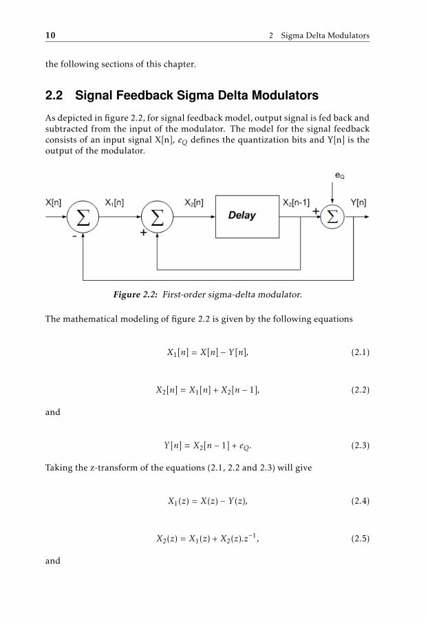
As depicted in figure 2.2, for signal feedback model, output signal is fed back andsubtracted from the input of the modulator. The model for the signal feedbackconsists of an input signal X[n], eQ defines the quantization bits and Y[n] is theoutput of the modulator.
Figure 2.2: First-order sigma-delta modulator.
The mathematical modeling of figure 2.2 is given by the following equations
X1[n] = X[n] − Y [n], (2.1)
X2[n] = X1[n] + X2[n − 1], (2.2)
and
Y [n] = X2[n − 1] + eQ. (2.3)
Taking the z-transform of the equations (2.1, 2.2 and 2.3) will give
X1(z) = X(z) − Y (z), (2.4)
X2(z) = X1(z) + X2(z).z−1, (2.5)
and
2.2 Signal Feedback Sigma Delta Modulators 11
Y (z) = X2(z)z−1 + eQ (2.6)
output, respectively. The output Y(z) of the model is calculated by solving theequations (2.4, 2.5 and 2.6) in terms of X(z) and eQ. The output Y(z) is given by
Y (z) = Y (z) = X(z)z−1 + eQ(1 − z−1). (2.7)
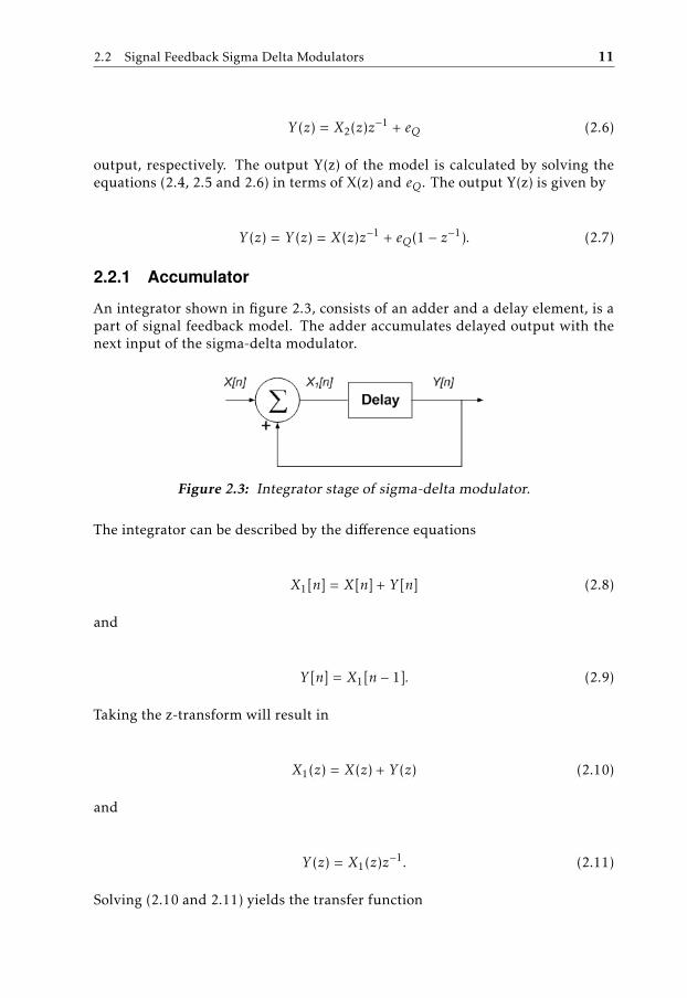
2.2.1 Accumulator
An integrator shown in figure 2.3, consists of an adder and a delay element, is apart of signal feedback model. The adder accumulates delayed output with thenext input of the sigma-delta modulator.
Figure 2.3: Integrator stage of sigma-delta modulator.
The integrator can be described by the difference equations
X1[n] = X[n] + Y [n] (2.8)
and
Y [n] = X1[n − 1]. (2.9)
Taking the z-transform will result in
X1(z) = X(z) + Y (z) (2.10)
and
Y (z) = X1(z)z−1. (2.11)
Solving (2.10 and 2.11) yields the transfer function

12 2 Sigma Delta Modulators
Y (z)X(z)
=z−1
1 − z−1 . (2.12)
Figure 2.4: Model of Sigma Delta Modulator Indicating where the Integratoris Placed.
2.2.2 Quantizer
The next component which is a part of the first-order sigma-delta modulator isa quantizer. The quantizer used in the modulator is shown in figure 2.5. Inthe model of sigma-delta modulator we assume that the quantization noise isnot correlated with the input signal [Janssen E. [2011]]. The quantizer can bemodeled as a block that has a linear gain and independent noise source whichadds quantization noise as shown in figure 2.5.
Figure 2.5: Quantizer stage of SDM.
2.2.3 Feedback Loop
The last part of sigma-delta modulator is a feedback loop. Sigma-delta modula-tors modify the spectral properties of the quantization noise, in such a way thatthe quantization noise is low in the band of interest. The modulator also tries tomove or shape the noise contents to higher frequencies, and this noise shaping isachieved with the help of a negative feedback loop.
If the integrator in the signal feedback model is replaced with a filter having atransfer function z−1 and the quantizer with N(z) as shown in figure 2.6 [Janssen E.[2011]]; then the transfer function for the modulator can be derived from
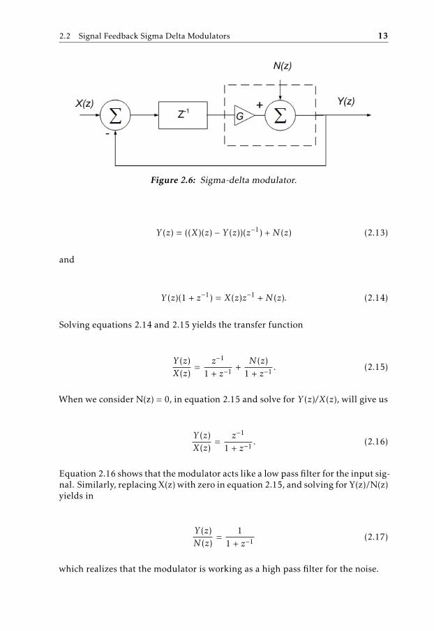
2.2 Signal Feedback Sigma Delta Modulators 13
Figure 2.6: Sigma-delta modulator.
Y (z) = ((X)(z) − Y (z))(z−1) + N (z) (2.13)
and
Y (z)(1 + z−1) = X(z)z−1 + N (z). (2.14)
Solving equations 2.14 and 2.15 yields the transfer function
Y (z)X(z)
=z−1
1 + z−1 +N (z)
1 + z−1 . (2.15)
When we consider N(z) = 0, in equation 2.15 and solve for Y (z)/X(z), will give us
Y (z)X(z)
=z−1
1 + z−1 . (2.16)
Equation 2.16 shows that the modulator acts like a low pass filter for the input sig-nal. Similarly, replacing X(z) with zero in equation 2.15, and solving for Y(z)/N(z)yields in
Y (z)N (z)
=1
1 + z−1 (2.17)
which realizes that the modulator is working as a high pass filter for the noise.
14 2 Sigma Delta Modulators
2.3 Error Feedback Sigma Delta Modulators
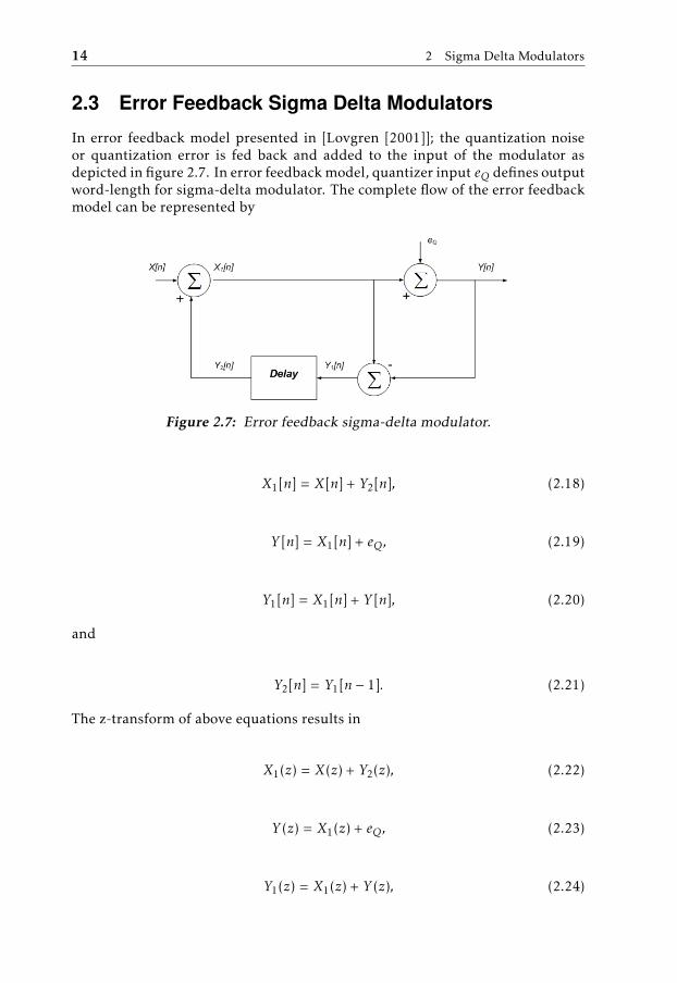
In error feedback model presented in [Lovgren [2001]]; the quantization noiseor quantization error is fed back and added to the input of the modulator asdepicted in figure 2.7. In error feedback model, quantizer input eQ defines outputword-length for sigma-delta modulator. The complete flow of the error feedbackmodel can be represented by
Figure 2.7: Error feedback sigma-delta modulator.
X1[n] = X[n] + Y2[n], (2.18)
Y [n] = X1[n] + eQ, (2.19)
Y1[n] = X1[n] + Y [n], (2.20)
and
Y2[n] = Y1[n − 1]. (2.21)
The z-transform of above equations results in
X1(z) = X(z) + Y2(z), (2.22)
Y (z) = X1(z) + eQ, (2.23)
Y1(z) = X1(z) + Y (z), (2.24)
2.4 Second-Order Signal Feedback Model 15
and
Y2(z) = Y (z)Z−1. (2.25)
The output Y(z) is represented as
Y (z) = X(z) + eQ(1 − z−1). (2.26)
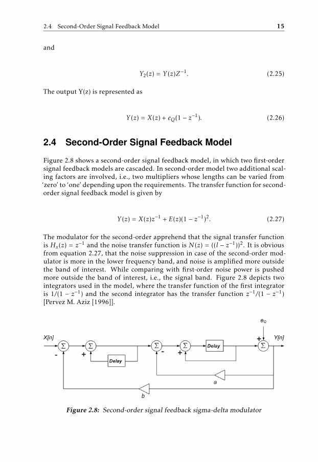
2.4 Second-Order Signal Feedback Model
Figure 2.8 shows a second-order signal feedback model, in which two first-ordersignal feedback models are cascaded. In second-order model two additional scal-ing factors are involved, i.e., two multipliers whose lengths can be varied from‘zero’ to ‘one’ depending upon the requirements. The transfer function for second-order signal feedback model is given by
Y (z) = X(z)z−1 + E(z)(1 − z−1)2. (2.27)
The modulator for the second-order apprehend that the signal transfer functionis Hx(z) = z−1 and the noise transfer function is N (z) = ((l − z−1))2. It is obviousfrom equation 2.27, that the noise suppression in case of the second-order mod-ulator is more in the lower frequency band, and noise is amplified more outsidethe band of interest. While comparing with first-order noise power is pushedmore outside the band of interest, i.e., the signal band. Figure 2.8 depicts twointegrators used in the model, where the transfer function of the first integratoris 1/(1 − z−1) and the second integrator has the transfer function z−1/(1 − z−1)[Pervez M. Aziz [1996]].
Figure 2.8: Second-order signal feedback sigma-delta modulator

16 2 Sigma Delta Modulators
2.5 Conclusion
In this chapter different topologies of sigma-delta modulators were discussed.The discussion is based on a detailed analysis of various components within thesigma-delta modulators.
Part III
Processing Model for SDM

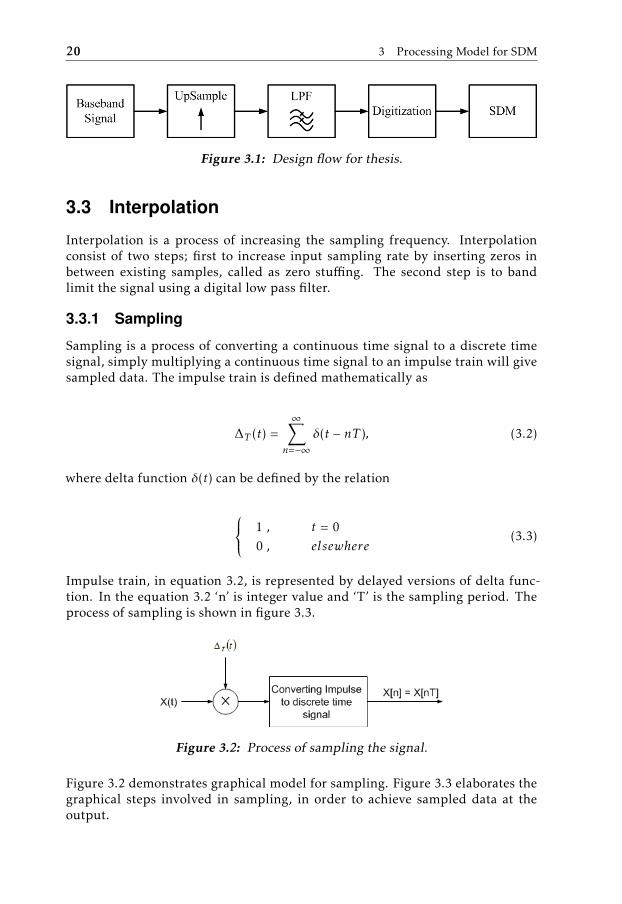
3Processing Model for SDM
3.1 Introduction
Testing and comparing results of the modulators are the important parts of thisthesis. Without verification of the modulators, it is hard to choose between differ-ent available modulator topologies. This chapter presents a complete processingmodel for the modulators which includes, baseband signal generation, interpola-tion of the signal, digitizing up-sampled signal and simulating the modulators.
3.2 Signal Generation
In signal generation block a continuous time coherent signal is generated andthat signal can be characterized by
X(t) = Asin(2πf t + φ), (3.1)
where ‘A’ is the amplitude which defines voltage swing of sine function, ‘f’ is thefrequency corresponding to the number of times a signal repeats itself in unittime and φ represents the phase of the signal. There are some other parametersrelated to the signal; one of them is bandwidth. The bandwidth can also be de-fined as range of frequencies an electronic signal uses over an electronic mediumfor its transmission.
19
20 3 Processing Model for SDM
Figure 3.1: Design flow for thesis.
3.3 Interpolation
Interpolation is a process of increasing the sampling frequency. Interpolationconsist of two steps; first to increase input sampling rate by inserting zeros inbetween existing samples, called as zero stuffing. The second step is to bandlimit the signal using a digital low pass filter.
3.3.1 Sampling
Sampling is a process of converting a continuous time signal to a discrete timesignal, simply multiplying a continuous time signal to an impulse train will givesampled data. The impulse train is defined mathematically as
∆T (t) =∞∑
n=−∞δ(t − nT ), (3.2)
where delta function δ(t) can be defined by the relation
1 , t = 00 , elsewhere
(3.3)
Impulse train, in equation 3.2, is represented by delayed versions of delta func-tion. In the equation 3.2 ‘n’ is integer value and ‘T’ is the sampling period. Theprocess of sampling is shown in figure 3.3.
Figure 3.2: Process of sampling the signal.
Figure 3.2 demonstrates graphical model for sampling. Figure 3.3 elaborates thegraphical steps involved in sampling, in order to achieve sampled data at theoutput.

3.3 Interpolation 21
Figure 3.3: Graphical explanation of sampling process.
Figure 3.2 and figure 3.3 explains graphical steps involved in sampling. For de-tailed mathematical analysis, sampled signal can be represented by
Xs(t) = X(t)δT (t), (3.4)
where Xs(t) is the sampled output, X(t) is the continuous signal and δT (t) is theimpulse train. Now substituting value of δT (t) from equation 3.2 in equation 3.4will result in sampled signal in time domain as
Xs(t) =∞∑
n=−∞X(t)δ(t − nT ). (3.5)
In time domain these signals are multiplied while in frequency domain thesesignals are convolved. For frequency domain analysis, the Fourier transform isused and the Fourier transform of equation 3.5 is
Xs(jΩ) =1
2πX(jΩ)δT (iΩ) (3.6)
and the Fourier transform of the impulse train is
δT (jΩ) =2πT
∞∑n=−∞
δ(Ω− nΩs). (3.7)
Substituting value from equation 3.7 to equation 3.6 will result in
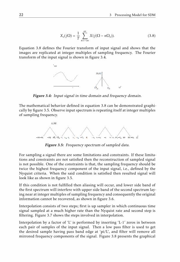
22 3 Processing Model for SDM
Xs(jΩ) =1T
∞∑n=−∞
X(j(Ω− nΩs)). (3.8)
Equation 3.8 defines the Fourier transform of input signal and shows that theimages are replicated at integer multiples of sampling frequency. The Fouriertransform of the input signal is shown in figure 3.4.
Figure 3.4: Input signal in time domain and frequency domain.
The mathematical behavior defined in equation 3.8 can be demonstrated graphi-cally by figure 3.5. Observe input spectrum is repeating itself at integer multiplesof sampling frequency.
Figure 3.5: Frequency spectrum of sampled data.
For sampling a signal there are some limitations and constraints. If these limita-tions and constraints are not satisfied then the reconstruction of sampled signalis not possible. One of the constraints is that, the sampling frequency should betwice the highest frequency component of the input signal, i.e., defined by theNyquist criteria. When the said condition is satisfied then resulted signal willlook like as shown in figure 3.5.
If this condition is not fulfilled then aliasing will occur, and lower side band ofthe first spectrum will interfere with upper side band of the second spectrum lay-ing near at integer multiples of sampling frequency and consequently the originalinformation cannot be recovered, as shown in figure 3.6.
Interpolation consists of two steps; first is up sampler in which continuous timesignal sampled at a much higher rate than the Nyquist rate and second step isfiltering. Figure 3.7 shows the steps involved in interpolation.
Interpolation by a factor of ‘L’ is performed by inserting ‘L-1’ zeros in betweeneach pair of samples of the input signal. Then a low pass filter is used to getthe desired sample having pass band edge at ‘pi/L’, and filter will remove allmirrored frequency components of the signal. Figure 3.8 presents the graphical

3.3 Interpolation 23
Figure 3.6: Concept of aliasing.
Figure 3.7: Interpolation.
concept of interpolation when a continuous time signal is interpolated by a factorof ‘L’ equals to “three”.
Figure 3.8 shows x(n) which is achieved through uniform sampling in which thesampling frequency is fs = 1/T , i.e., x(n) = xc(nT ). From x(n) a new sequence isobtained in which the sampling frequency is ‘L’ times higher than the uniformsampling, i.e., Y (m) = xc(mT /L). The sampling period for the signal x(n) was ‘T’,and now after interpolation the sampling period for w(m) is reduced to T 1 = T /L[Lowenborg [2006]].
For frequency domain analysis the Fourier transform of w(m) is given by
W (ejωT1 ) =∞∑
m=−∞w(m)e−jωT1m, (3.9)
the Fourier transform of W(n) in terms of x(n) is represented as
W (ejωT1 ) =∞∑
n=−∞x(n)e−jωT1Ln. (3.10)
and the Fourier transform of signal x(n) is given by
X(ejωT ) =∞∑
n=−∞x(n)e−jωT n. (3.11)
Figure 3.9 from [Lowenborg [2006]] shows graphical steps involved in interpola-tion, initially the signal is interpolated by a factor of L, and then digitally filtered

24 3 Processing Model for SDM
(a) (b)
(c)
Figure 3.8: Steps involved in interpolation.
with the help of low pass filter.
Up sampling is performed to increase the sampling frequency. The process alsoincreases signal to noise ratio (SNR) as defined as
SNR = 6.02 ·NOB + 1.76 + 10 · log(OSR), (3.12)
where in equation 3.12 the term NOB is the number of quantization bits alsodefined as word-length. Oversampling ratio (OSR) can be defined as the ratiobetween sampling frequency ‘f ′sample and base band signal bandwidth [Afzal N[2010]]
OSR =fsample
2 · “Bandwidth′′. (3.13)
3.3.2 Digitization
Digitization is the process of converting continuous time signal which can beconsidered as information or up sampled data into digital format. In digital for-mat input data (up sampled) is structured into discrete units of data that can betermed as bits, and those bits can be separately addressed. After up samplingand filtering, the signal is digitized. [Afzal N [2010]] states that the input word-length (NOB) has a direct impact on signal to noise ratio (SNR), and the relationcan be defined by
3.4 Conclusion 25
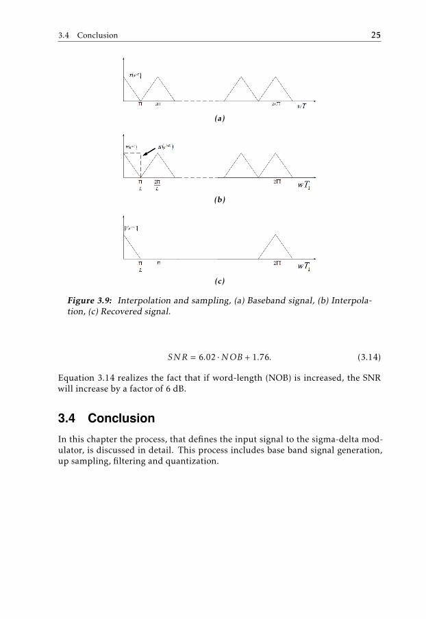
(a)
(b)
(c)
Figure 3.9: Interpolation and sampling, (a) Baseband signal, (b) Interpola-tion, (c) Recovered signal.
SNR = 6.02 ·NOB + 1.76. (3.14)
Equation 3.14 realizes the fact that if word-length (NOB) is increased, the SNRwill increase by a factor of 6 dB.
3.4 Conclusion
In this chapter the process, that defines the input signal to the sigma-delta mod-ulator, is discussed in detail. This process includes base band signal generation,up sampling, filtering and quantization.

Part IV
Digital Modelling of SDM


4Digital Modeling of SDM
4.1 Introduction
This chapter discusses digital modeling of the sigma-delta modulators which aredescribed in chapter 2. The aim of this thesis is to implement a reconfigurablesigma delta modulator in hardware. The hardware implementation of sigmadelta modulator means the design is implemented using automatically generatedlayouts.
The layout design is quite laborious which requires long design time if done man-ually. To skip the manual layout design process and minimize design effort; adesign tool from Cadence® named SoC Encounter is used. This tool minimizesthe effort of layout design by automatically generating layout design from Verilognetlist.
4.2 SoC Encounter Design Flow
In this thesis, a reconfigurable sigma-delta modulator is designed, which is a partof all-digital DACs. The sigma-delta modulator is designed using RTL language,i.e., Verilog. SoC Encounter is then used to generate a layout design from Verilognetlist, generated by a tool named Design Compiler. The complete design flow ofSoC Encounter is shown in figure 4.1.
Encounter has three types of input files; one is Verilog netlist file which is gen-erated using a Design Compiler. The Design Compiler is an RTL synthesis toolfrom Synopsys which is used to convert RTL design file into Verilog netlist. Thecompiler takes care of the timing information and the standard cells that will beplaced during layout generation process. The second input is timing information
29

30 4 Digital Modeling of SDM
Figure 4.1: Steps involved in designing layout using SoC Encounter.
4.3 Design Libraries 31
file (*.tlf), which contains timing information of the standard cells available incurrent standard cells library; provided by the foundry. The last file used to im-port design in Encounter is Library Export Format (LEF) file. These files containdefinitions of routing layers, vias, metal capacitances and design rules etc.
In the second step, floor planning is performed. While floor planning one shouldknow available core size, size of the chip and location of IO ports. The floorplan defines outer boundaries of the chip being designed. Power planning stepdefines how power will be distributed throughout the chip. There are severalways to distribute power in chip, which are explained in detail in section 6.4.3 ofchapter 6.
In the next step the standard cells are placed and optimized for timing. Anydifferences in clock phase delays will be removed in this step by adding invertersand buffers in design. The design is then routed and once again checked for theclock phase delays.
After routing and optimizing design for the timing constraints it is necessary toverify the design. There are several verification options available like connectiv-ity verification, geometry verification and design rule check (DRC) verification toverify successful placement of the design.
After successful verification of the design, final step is to export the design in*.gds file and netlist (*.v) file. This new netlist also contains the inverters andbuffers added in timing optimization process. The *.gds file can be used to importlayout in cadence and both netlist files can be used to import design schematic incadence.
4.3 Design Libraries
While working with Encounter; the choice of libraries is one of the critical stepsof designing. Several libraries are available in Encounter kit with different speci-fications of power, voltage, speed and leakage; some of the available libraries areGPHVT, GPLVT, GPSVT, LPHVT, LPLVT and LPSVT.
GP libraries are the fastest libraries while the LVT libraries provide good perfor-mance at high data rates. There is a trade-off between speed and power leakage.With increase in the speed, the leakage will also be increased. So the HVT optionstypically give best performance in terms of speed and power leakage [Pullini. A[2007]].
The modulators presented in this thesis are intended to be used with high speedapplications. Leakage is desired to be reduced for high speed applications; so thelibraries used in this thesis were from CORE65GPHVT library. GP are the fastestand HVT will provide the best performance as compared with speed.
32 4 Digital Modeling of SDM
4.4 Top Model of Sigma Delta Modulator
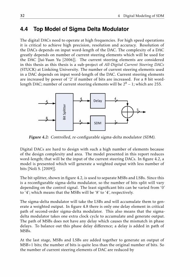
The digital DACs need to operate at high frequencies. For high speed operationsit is critical to achieve high precision, resolution and accuracy. Resolution ofthe DACs depends on input word-length of the DAC. The complexity of a DACgreatly depends on number of current steering elements which will be used forthe DAC [Jui-Yuan Yu [2006]]. The current steering elements are consideredin this thesis as this thesis is a sub-project of All-Digital Current Steering DACs(STUCK) at Linköing University. The number of current steering elements usedin a DAC depends on input word-length of the DAC. Current steering elementsare increased by power of ‘2’ if number of bits are increased. For a 8 bit word-length DAC; number of current steering elements will be 28 − 1; which are 255.
Figure 4.2: Controlled, re-configurable sigma-delta modulator (SDM).
Digital DACs are hard to design with such a high number of elements becauseof the design complexity and area. The model presented in this report reducesword-length; that will be the input of the current steering DACs. In figure 4.2, amodel is presented which will generate a weighted output with less number ofbits [Noli S. [2009]].
The bit splitter, shown in figure 4.2, is used to separate MSBs and LSBs. Since thisis a reconfigurable sigma-delta modulator, so the number of bits split will varydepending on the control signal. The least significant bits can be varied from ‘0’to ‘4’; which means that the MSBs will be ‘8’ to ‘4’, respectively.
The sigma-delta modulator will take the LSBs and will accumulate them to gen-erate a weighted output. In figure 4.8 there is only one delay element in criticalpath of second-order sigma-delta modulator. This also means that the sigma-delta modulator takes one extra clock cycle to accumulate and generate output.The path of MSBs does not have any delay which causes the mismatch in phasedelays. To balance out this phase delay difference; a delay is added in path ofMSBs.
At the last stage, MSBs and LSBs are added together to generate an output ofMSB+1 bits; the number of bits is quite less than the original number of bits. Sothe number of current steering elements of DAC are reduced by

4.5 Design of Re-Configurable Digital Sigma Delta Modulator 33
“ElementsReduced′′ = 2NOB − 1 − 2MSB+1. (4.1)
The ‘1’ in equation 4.1 comes from the fact that the LSBs are reduced to ‘1’. TheLSB requires only one current steering element in DAC. So the total number ofelements will be
“Numberof Elements′′ = 2MSB+1. (4.2)
In figure 4.2 consider MSBs and LSBs are ‘4’; so reduced number of elements forDAC are 32.
4.5 Design of Re-Configurable Digital Sigma DeltaModulator
The sigma-delta modulator presented in section 4.4 is reconfigurable, which meansthat the length of the modulator can be controlled with the input control signal.The purpose of this reconfigurable SDM is to use same SDM for different inputword lengths. Functionality and design of the SDM is presented in this section.
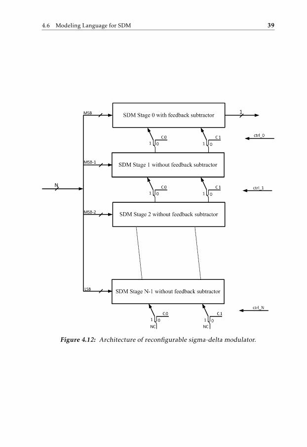
The modulator can be divided in two major blocks as shown in figure 4.3, one iscalled stage0 sigma-delta modulator and the other is stageN sigma-delta modula-tor (SDM).
Figure 4.3: Sub-blocks of non-configurable sigma-delta modulator.
34 4 Digital Modeling of SDM
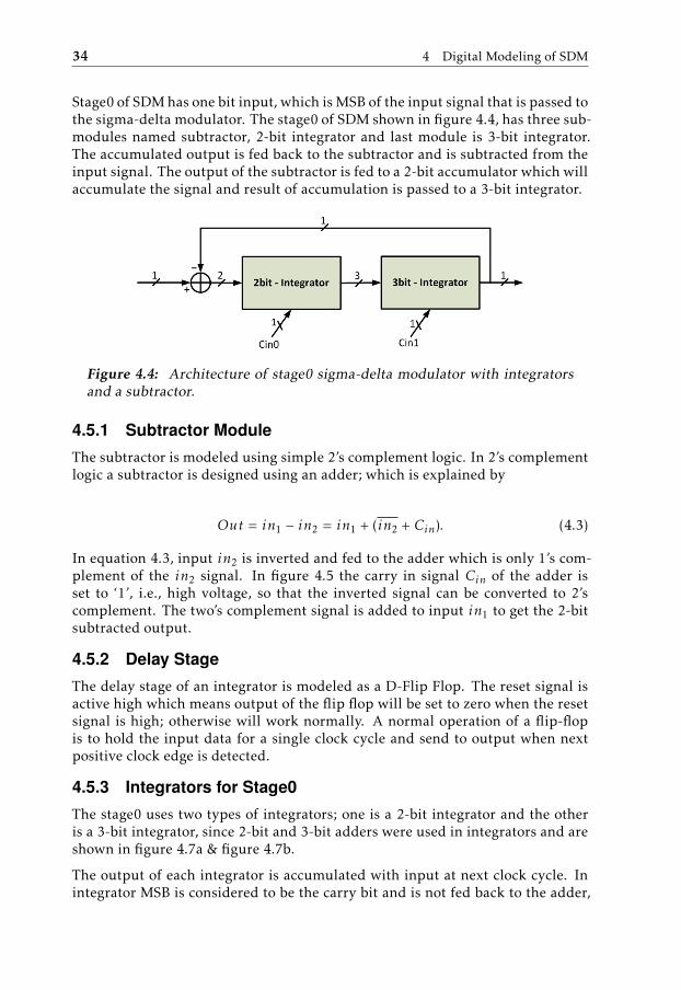
Stage0 of SDM has one bit input, which is MSB of the input signal that is passed tothe sigma-delta modulator. The stage0 of SDM shown in figure 4.4, has three sub-modules named subtractor, 2-bit integrator and last module is 3-bit integrator.The accumulated output is fed back to the subtractor and is subtracted from theinput signal. The output of the subtractor is fed to a 2-bit accumulator which willaccumulate the signal and result of accumulation is passed to a 3-bit integrator.
Figure 4.4: Architecture of stage0 sigma-delta modulator with integratorsand a subtractor.
4.5.1 Subtractor Module
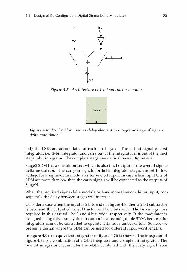
The subtractor is modeled using simple 2’s complement logic. In 2’s complementlogic a subtractor is designed using an adder; which is explained by
Out = in1 − in2 = in1 + (in2 + Cin). (4.3)
In equation 4.3, input in2 is inverted and fed to the adder which is only 1’s com-plement of the in2 signal. In figure 4.5 the carry in signal Cin of the adder isset to ‘1’, i.e., high voltage, so that the inverted signal can be converted to 2’scomplement. The two’s complement signal is added to input in1 to get the 2-bitsubtracted output.
4.5.2 Delay Stage
The delay stage of an integrator is modeled as a D-Flip Flop. The reset signal isactive high which means output of the flip flop will be set to zero when the resetsignal is high; otherwise will work normally. A normal operation of a flip-flopis to hold the input data for a single clock cycle and send to output when nextpositive clock edge is detected.
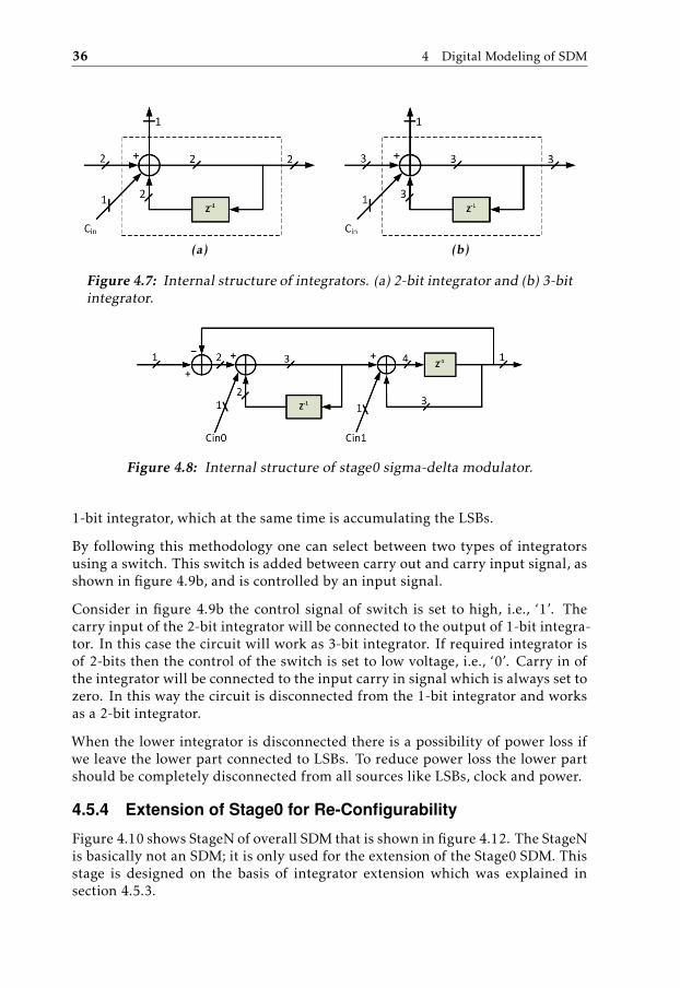
4.5.3 Integrators for Stage0
The stage0 uses two types of integrators; one is a 2-bit integrator and the otheris a 3-bit integrator, since 2-bit and 3-bit adders were used in integrators and areshown in figure 4.7a & figure 4.7b.
The output of each integrator is accumulated with input at next clock cycle. Inintegrator MSB is considered to be the carry bit and is not fed back to the adder,
4.5 Design of Re-Configurable Digital Sigma Delta Modulator 35
Figure 4.5: Architecture of 1-bit subtractor module.
Figure 4.6: D-Flip Flop used as delay element in integrator stage of sigma-delta modulator.
only the LSBs are accumulated at each clock cycle. The output signal of firstintegrator, i.e., 2-bit integrator and carry out of the integrator is input of the nextstage 3-bit integrator. The complete stage0 model is shown in figure 4.8.
Stage0 SDM has a one bit output which is also final output of the overall sigma-delta modulator. The carry-in signals for both integrator stages are set to lowvoltage for a sigma-delta modulator for one bit input. In case when input bits ofSDM are more than one then the carry signals will be connected to the outputs ofStageN.
When the required sigma-delta modulator have more than one bit as input, con-sequently the delay between stages will increase.
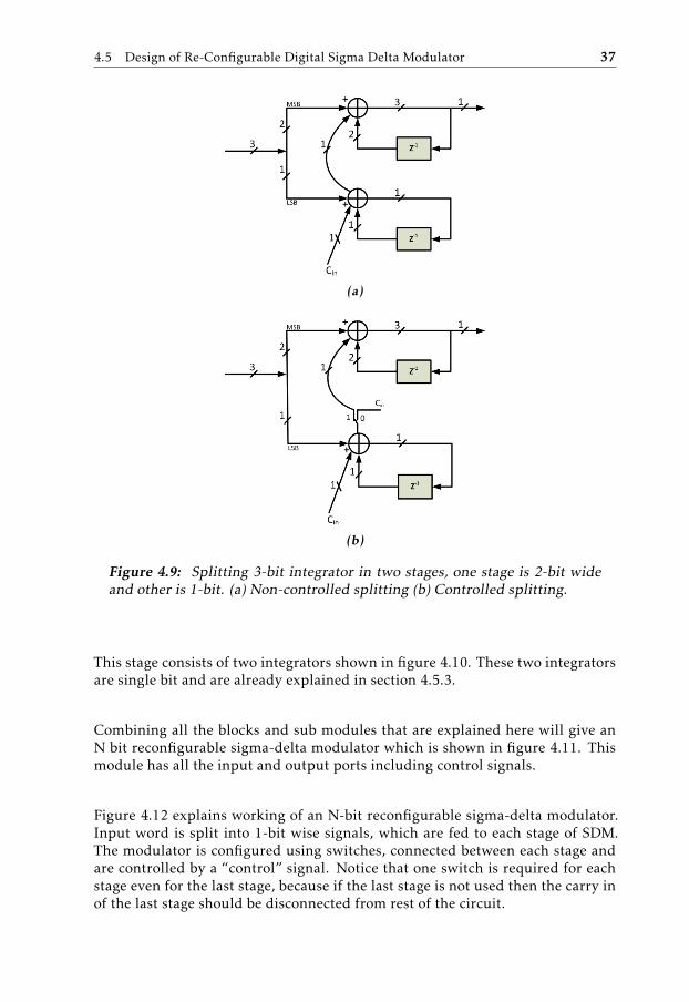
Consider a case when the input is 2 bits wide in figure 4.8, then a 2 bit subtractoris used and the output of the subtractor will be 3 bits wide. The two integratorsrequired in this case will be 3 and 4 bits wide, respectively. If the modulator isdesigned using this strategy then it cannot be a reconfigurable SDM, because theintegrators cannot be controlled to operate with less number of bits. So here wepresent a design where the SDM can be used for different input word lengths.
In figure 4.9a an equivalent integrator of figure 4.7b is shown. The integrator offigure 4.9a is a combination of a 2-bit integrator and a single bit integrator. Thetwo bit integrator accumulates the MSBs combined with the carry signal from
36 4 Digital Modeling of SDM
(a) (b)
Figure 4.7: Internal structure of integrators. (a) 2-bit integrator and (b) 3-bitintegrator.
Figure 4.8: Internal structure of stage0 sigma-delta modulator.
1-bit integrator, which at the same time is accumulating the LSBs.
By following this methodology one can select between two types of integratorsusing a switch. This switch is added between carry out and carry input signal, asshown in figure 4.9b, and is controlled by an input signal.
Consider in figure 4.9b the control signal of switch is set to high, i.e., ‘1’. Thecarry input of the 2-bit integrator will be connected to the output of 1-bit integra-tor. In this case the circuit will work as 3-bit integrator. If required integrator isof 2-bits then the control of the switch is set to low voltage, i.e., ‘0’. Carry in ofthe integrator will be connected to the input carry in signal which is always set tozero. In this way the circuit is disconnected from the 1-bit integrator and worksas a 2-bit integrator.
When the lower integrator is disconnected there is a possibility of power loss ifwe leave the lower part connected to LSBs. To reduce power loss the lower partshould be completely disconnected from all sources like LSBs, clock and power.
4.5.4 Extension of Stage0 for Re-Configurability
Figure 4.10 shows StageN of overall SDM that is shown in figure 4.12. The StageNis basically not an SDM; it is only used for the extension of the Stage0 SDM. Thisstage is designed on the basis of integrator extension which was explained insection 4.5.3.
4.5 Design of Re-Configurable Digital Sigma Delta Modulator 37
(a)
(b)
Figure 4.9: Splitting 3-bit integrator in two stages, one stage is 2-bit wideand other is 1-bit. (a) Non-controlled splitting (b) Controlled splitting.
This stage consists of two integrators shown in figure 4.10. These two integratorsare single bit and are already explained in section 4.5.3.
Combining all the blocks and sub modules that are explained here will give anN bit reconfigurable sigma-delta modulator which is shown in figure 4.11. Thismodule has all the input and output ports including control signals.
Figure 4.12 explains working of an N-bit reconfigurable sigma-delta modulator.Input word is split into 1-bit wise signals, which are fed to each stage of SDM.The modulator is configured using switches, connected between each stage andare controlled by a “control” signal. Notice that one switch is required for eachstage even for the last stage, because if the last stage is not used then the carry inof the last stage should be disconnected from rest of the circuit.

38 4 Digital Modeling of SDM
Figure 4.10: Structure of stageN used for extension of stage0 for high orderSDM.
Figure 4.11: Top symbol of re-configurable sigma-delta modulator.
4.5.5 Pipelining for Higher Number of Bits
When the number of input bits, i.e., word-length increases, the delay betweenSDM stages will also increase. Increased word-length will also affect the addermodule. The adder works on the logic of adding two bits and passes the carryto the next adder, which might result in delayed carry propagation till the laststages of the adder.
Pipeline adders are used for high speed DSDM [Bhansali P. [2006]]. The pipelineadders may be introduced between SDM stages. In this thesis the input word-length is not large enough to consider this problem, so the pipelining issue is notconsidered in this thesis work.
4.6 Modeling Language for SDM
The complete model of the modulator is designed in MODELSIM using RTL lan-guage. There are two basic modules, subtractor and integrator for each stage insigma-delta modulator. The integrators are further divided into delay elementsand adders. The division of the modules in different sub blocks made coding ofmodules easy.
4.6 Modeling Language for SDM 39
Figure 4.12: Architecture of reconfigurable sigma-delta modulator.
40 4 Digital Modeling of SDM
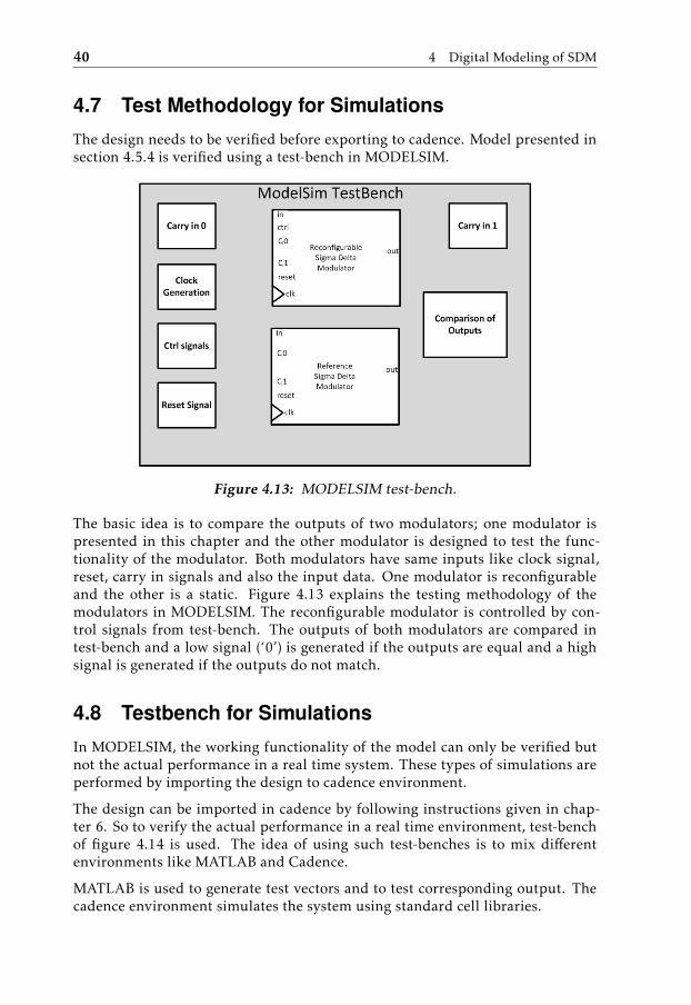
4.7 Test Methodology for Simulations
The design needs to be verified before exporting to cadence. Model presented insection 4.5.4 is verified using a test-bench in MODELSIM.
Figure 4.13: MODELSIM test-bench.
The basic idea is to compare the outputs of two modulators; one modulator ispresented in this chapter and the other modulator is designed to test the func-tionality of the modulator. Both modulators have same inputs like clock signal,reset, carry in signals and also the input data. One modulator is reconfigurableand the other is a static. Figure 4.13 explains the testing methodology of themodulators in MODELSIM. The reconfigurable modulator is controlled by con-trol signals from test-bench. The outputs of both modulators are compared intest-bench and a low signal (‘0’) is generated if the outputs are equal and a highsignal is generated if the outputs do not match.
4.8 Testbench for Simulations
In MODELSIM, the working functionality of the model can only be verified butnot the actual performance in a real time system. These types of simulations areperformed by importing the design to cadence environment.
The design can be imported in cadence by following instructions given in chap-ter 6. So to verify the actual performance in a real time environment, test-benchof figure 4.14 is used. The idea of using such test-benches is to mix differentenvironments like MATLAB and Cadence.
MATLAB is used to generate test vectors and to test corresponding output. Thecadence environment simulates the system using standard cell libraries.

4.8 Testbench for Simulations 41
Figu
re4.14
:Te
stm
etho
dol
ogy
for
re-c
onfi
gura
ble
SDM
usi
ngM
AT
LA
Ban
dC
aden
ce.

42 4 Digital Modeling of SDM
(a) (b)
Figure 4.15: MATLAB environment (a) Generate baseband signal, (b) Postprocessing after simulations.
4.8.1 MATLAB Environment
MATLAB is used to perform two tasks one is to generate the input signal and theother is to post process the output after simulations; which is to test the output ofthe modulators. As shown in figure 4.15a, signal generation block will generatea digital base band signal. As the modulator is intended to work for 2 GHz fre-quency, so the sampling frequency of the input signal is 2 GHz and the basebandsignal is at 50 MHz.
The other task of MATLAB is to analyze the data after simulations in cadence.The simulated output is read through a text file.
4.8.2 Interfaces
The interfaces shown in figure 4.16 provide a link between MATLAB and Ca-dence. Text file which has input data, is read by file-reader of figure 4.16a. Thisinput data is fed to the sigma-delta modulator. The file reader also needs a clockof the same frequency as sampling frequency of the data; as this clock also definesthe data rate of the input signal.
The output of the sigma-delta modulator is stored in a file using a file-writer. Thefile writer writes the data in text file and is read by MATLAB for post processing.The file writer writes the data in binary form; which should be kept in mind whilereading the data in MATLAB. Again the clock frequency of the file-writer is alsosame as the sampling frequency of the input data.

4.8 Testbench for Simulations 43
(a) (b)
Figure 4.16: Interface between MATLAB and Cadence (a) Read-in data fromMATLAB, (b) Write-out data from Cadence.
4.8.3 Cadence Environment
In cadence real model of sigma-delta modulator is simulated. Carry signals, de-sign clock and the reset signals are generated in cadence. The control signalsgenerated in cadence enables the reconfigurability of the sigma-delta modulator.The control signal can select between ‘0’ to ‘4’ bits of sigma-delta modulator to betested. Having control signals in place it is possible to use sigma-delta modulatorfor ‘4’ bit input or the modulator can be completely bypassed.
The input of the SDM comes from the interface part of the test-bench and outputof the sigma-delta modulator is passed to other interface, i.e., file-writer.
Figure 4.17: Test-bench for real time simulations in Cadence.

44 4 Digital Modeling of SDM
4.9 Conclusion
This chapter presents the re-configurable sigma-delta modulator that can be usedfor variable input word lengths. The SDM can be controlled by the input controlsignal. A test methodology is also presented to check the working of sigma-deltamodulators for different environments like MODELSIM, MATLAB and Cadenceetc.

Part V
Simulation Results

5Simulation Results
5.1 Introduction
Up till now all the discussions were about selecting the right architecture forsigma-delta modulators and to model that architecture using RTL language. Test-ing models for re-configurable sigma-delta modulators are presented. This chap-ter presents simulation results of different modulator topologies and hardwareimplementation results.
5.2 Baseband Signal Generator
A function generation block is described previously in section 3.2 which gen-erates a coherent sine wave of 8.031250 MHz with fixed amplitude of 0.5 andbandwidth of 16 MHz as shown in figure 5.1. Frequency spectrum of the inputcoherent is shown in figure 5.2.
In figure 5.2 the first harmonic is observed at 8.031250 MHz and the second har-monic appears at (128 MHz – 8.031250 MHz) 119.968750 MHz, where 128 MHzis the sampling frequency.
5.3 Interpolation
According to the design flow described in section 3.3, baseband signal is fed tothe interpolation block, which over samples the signal by a factor of L. The in-terpolation factor is varied from 2 to 16, as multiples of 2. In this case initialoversampling ratio (OSR) is set to 4; before interpolation.
47

48 5 Simulation Results
Figure 5.1: Baseband signal of frequency 8 MHz.
Figure 5.2: Frequency spectrum of input baseband signal with samplingfrequency at 128 MHz.
5.4 Filtering 49
The OSR at output of the interpolator should be equal to 64. To achieve this OSR,i.e., 64, signal should be interpolated by a factor of 16 (L=16). This OSR alongwith the interpolation factor of 16 will give the sampling frequency of 2.04 GHzfor the modulator.
By varying the interpolation factor the sampling frequency is increased from128 MHz to 2.048 GHz, corresponding to the interpolation factor of 16.
Figure 5.3 shows interpolated signal by a factor of 16, where one can see that orig-inal signal (base band) will repeat itself at multiples of 128 MHz, i.e., 128 MHz,256 MHz and so on.
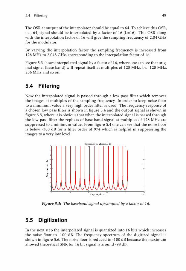
5.4 Filtering
Now the interpolated signal is passed through a low pass filter which removesthe images at multiples of the sampling frequency. In order to keep noise floorto a minimum value a very high order filter is used. The frequency response ofa chosen low pass filter is shown in figure 5.4 and the output signal is shown infigure 5.5, where it is obvious that when the interpolated signal is passed throughthe low pass filter the replicas of base band signal at multiples of 128 MHz aresuppressed to a minimum value. From figure 5.4 one can see that the noise flooris below -300 dB for a filter order of 974 which is helpful in suppressing theimages to a very low level.
Figure 5.3: The baseband signal upsampled by a factor of 16.
5.5 Digitization
In the next step the interpolated signal is quantized into 16 bits which increasesthe noise floor to -100 dB. The frequency spectrum of the digitized signal isshown in figure 5.6. The noise floor is reduced to -100 dB because the maximumallowed theoretical SNR for 16 bit signal is around -98 dB.

50 5 Simulation Results
Figure 5.4: Frequency response of anti-aliasing filter with order of 974.
Figure 5.5: Spectrum of output signal after anti-aliasing filter.
As shown in equation 3.12 in section 3.3.1 the SNR increases by a factor of 3 dBwith increase in OSR as a multiple of 2. Figure 5.7 shows the direct relation ofSNR and OSR. The simulated SNR cannot exceed -98 dB because of quantizationlimitations as shown in figure 5.7.
The equation depicting the relation between the number of quantization bits andSNR is given in section 3.3.2. From these equations observe that increasing thenumber of quantization bits improves the SNR. Theoretically for each additionalbit SNR increases by 6 dB.
Figure 5.8 shows the relationship of theoretical and simulated SNR, when quan-tization bits are varied. After a certain limit there is no effect of increasing quan-tization bits on the simulated SNR, because of the tool limitations. MATLAB canonly work for words that are 44 bits wide.
5.6 Sigma Delta Modulators
The digitized signal is input of the sigma-delta modulator as discussed in chapter2. Different types of SDM are used to study their noise shaping behavior of theinput signal.

5.6 Sigma Delta Modulators 51
Figure 5.6: Spectrum of digital signal with 16 word-length.
Figure 5.7: Comparison of signal to noise ratio (SNR) and over samplingratio.
52 5 Simulation Results
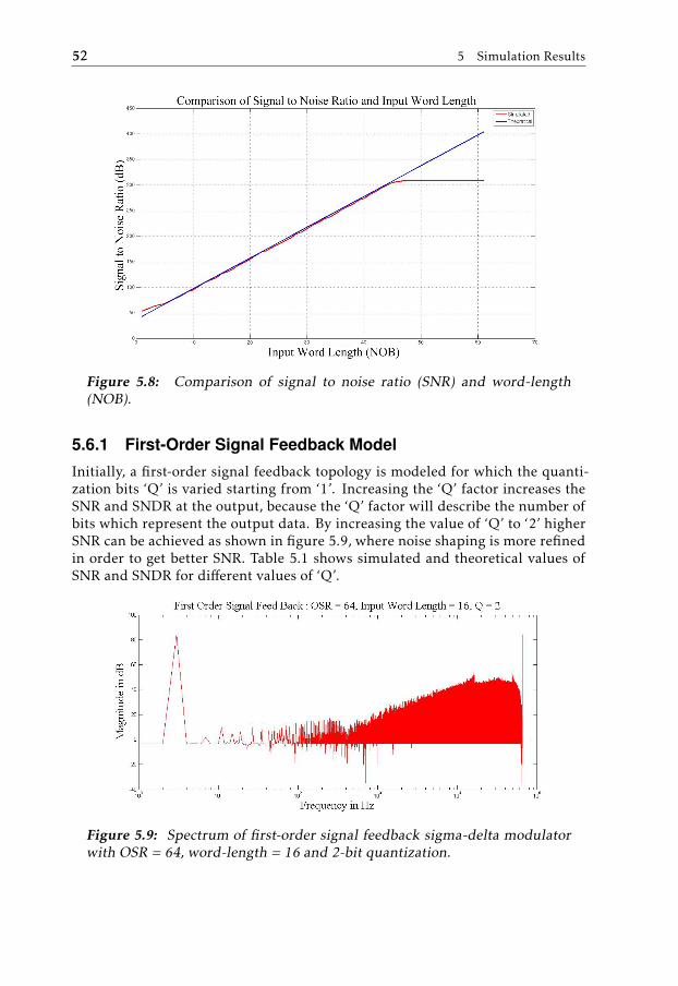
Figure 5.8: Comparison of signal to noise ratio (SNR) and word-length(NOB).
5.6.1 First-Order Signal Feedback Model
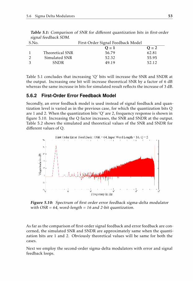
Initially, a first-order signal feedback topology is modeled for which the quanti-zation bits ‘Q’ is varied starting from ‘1’. Increasing the ‘Q’ factor increases theSNR and SNDR at the output, because the ‘Q’ factor will describe the number ofbits which represent the output data. By increasing the value of ‘Q’ to ‘2’ higherSNR can be achieved as shown in figure 5.9, where noise shaping is more refinedin order to get better SNR. Table 5.1 shows simulated and theoretical values ofSNR and SNDR for different values of ‘Q’.
Figure 5.9: Spectrum of first-order signal feedback sigma-delta modulatorwith OSR = 64, word-length = 16 and 2-bit quantization.
5.6 Sigma Delta Modulators 53
Table 5.1: Comparison of SNR for different quantization bits in first-ordersignal feedback SDM.
S.No. First-Order Signal Feedback ModelQ = 1 Q = 2
1 Theoretical SNR 56.79 62.812 Simulated SNR 52.32 55.953 SNDR 49.19 52.12
Table 5.1 concludes that increasing ‘Q’ bits will increase the SNR and SNDR atthe output. Increasing one bit will increase theoretical SNR by a factor of 6 dBwhereas the same increase in bits for simulated result reflects the increase of 3 dB.
5.6.2 First-Order Error Feedback Model
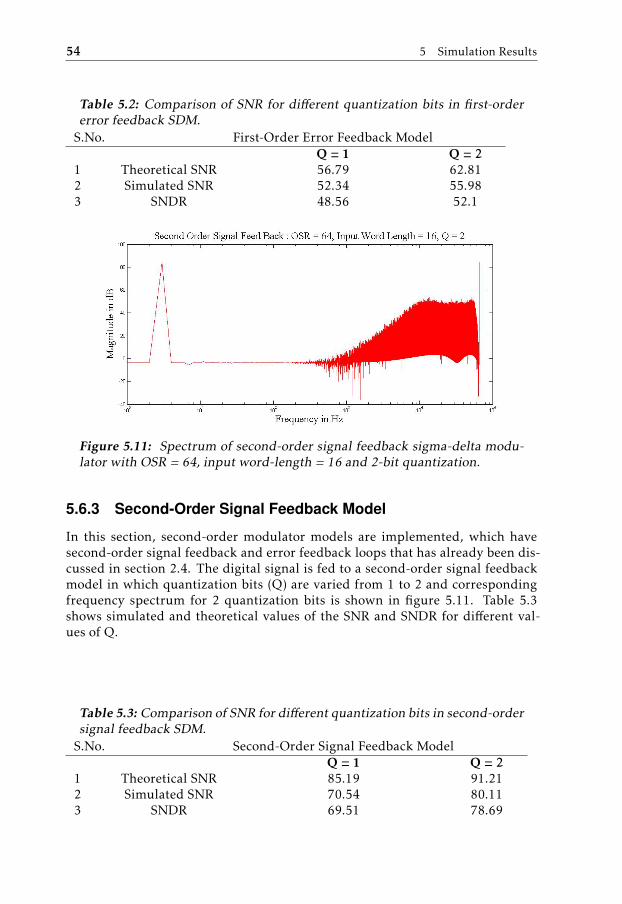
Secondly, an error feedback model is used instead of signal feedback and quan-tization level is varied as in the previous case, for which the quantization bits Qare 1 and 2. When the quantization bits ‘Q’ are 2, frequency response is shown infigure 5.10. Increasing the Q factor increases, the SNR and SNDR at the output.Table 5.2 shows the simulated and theoretical values of the SNR and SNDR fordifferent values of Q.
Figure 5.10: Spectrum of first order error feedback sigma-delta modulatorwith OSR = 64, word-length = 16 and 2-bit quantization.
As far as the comparison of first-order signal feedback and error feedback are con-cerned, the simulated SNR and SNDR are approximately same when the quanti-zation bits are 1 and 2. Obviously theoretical values will be same for both thecases.
Next we employ the second-order sigma-delta modulators with error and signalfeedback loops.
54 5 Simulation Results
Table 5.2: Comparison of SNR for different quantization bits in first-ordererror feedback SDM.
S.No. First-Order Error Feedback ModelQ = 1 Q = 2
1 Theoretical SNR 56.79 62.812 Simulated SNR 52.34 55.983 SNDR 48.56 52.1
Figure 5.11: Spectrum of second-order signal feedback sigma-delta modu-lator with OSR = 64, input word-length = 16 and 2-bit quantization.
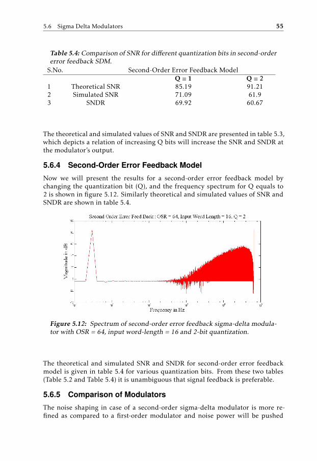
5.6.3 Second-Order Signal Feedback Model
In this section, second-order modulator models are implemented, which havesecond-order signal feedback and error feedback loops that has already been dis-cussed in section 2.4. The digital signal is fed to a second-order signal feedbackmodel in which quantization bits (Q) are varied from 1 to 2 and correspondingfrequency spectrum for 2 quantization bits is shown in figure 5.11. Table 5.3shows simulated and theoretical values of the SNR and SNDR for different val-ues of Q.
Table 5.3: Comparison of SNR for different quantization bits in second-ordersignal feedback SDM.
S.No. Second-Order Signal Feedback ModelQ = 1 Q = 2
1 Theoretical SNR 85.19 91.212 Simulated SNR 70.54 80.113 SNDR 69.51 78.69
5.6 Sigma Delta Modulators 55
Table 5.4: Comparison of SNR for different quantization bits in second-ordererror feedback SDM.
S.No. Second-Order Error Feedback ModelQ = 1 Q = 2
1 Theoretical SNR 85.19 91.212 Simulated SNR 71.09 61.93 SNDR 69.92 60.67
The theoretical and simulated values of SNR and SNDR are presented in table 5.3,which depicts a relation of increasing Q bits will increase the SNR and SNDR atthe modulator’s output.
5.6.4 Second-Order Error Feedback Model
Now we will present the results for a second-order error feedback model bychanging the quantization bit (Q), and the frequency spectrum for Q equals to2 is shown in figure 5.12. Similarly theoretical and simulated values of SNR andSNDR are shown in table 5.4.
Figure 5.12: Spectrum of second-order error feedback sigma-delta modula-tor with OSR = 64, input word-length = 16 and 2-bit quantization.
The theoretical and simulated SNR and SNDR for second-order error feedbackmodel is given in table 5.4 for various quantization bits. From these two tables(Table 5.2 and Table 5.4) it is unambiguous that signal feedback is preferable.
5.6.5 Comparison of Modulators
The noise shaping in case of a second-order sigma-delta modulator is more re-fined as compared to a first-order modulator and noise power will be pushed
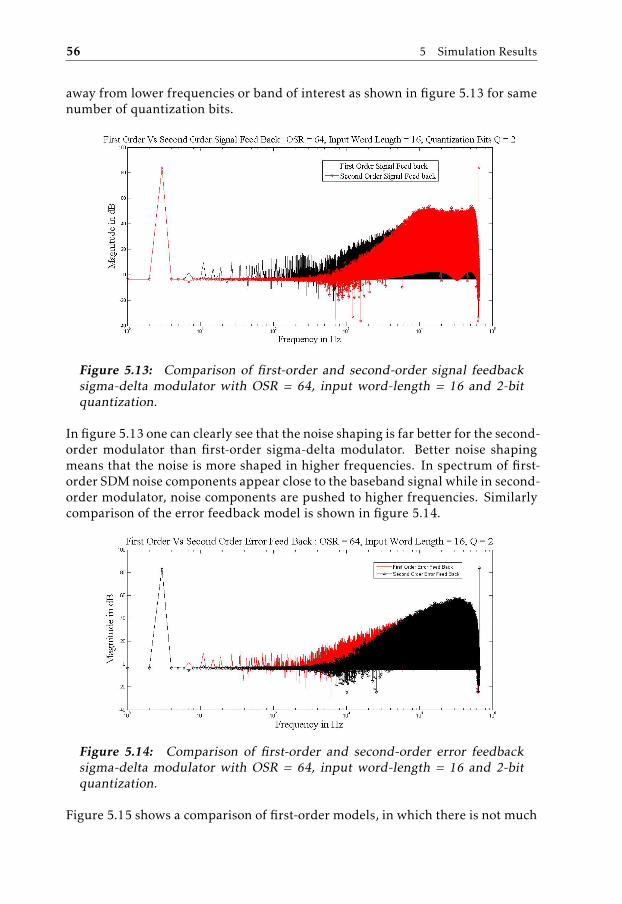
56 5 Simulation Results
away from lower frequencies or band of interest as shown in figure 5.13 for samenumber of quantization bits.
Figure 5.13: Comparison of first-order and second-order signal feedbacksigma-delta modulator with OSR = 64, input word-length = 16 and 2-bitquantization.
In figure 5.13 one can clearly see that the noise shaping is far better for the second-order modulator than first-order sigma-delta modulator. Better noise shapingmeans that the noise is more shaped in higher frequencies. In spectrum of first-order SDM noise components appear close to the baseband signal while in second-order modulator, noise components are pushed to higher frequencies. Similarlycomparison of the error feedback model is shown in figure 5.14.
Figure 5.14: Comparison of first-order and second-order error feedbacksigma-delta modulator with OSR = 64, input word-length = 16 and 2-bitquantization.
Figure 5.15 shows a comparison of first-order models, in which there is not much

5.7 Hardware Implementation Results 57
difference when the quantization bits (Q) are 2.
Figure 5.15: Comparison of First-Order Signal and Error Feedback SigmaDelta Modulator with OSR = 64, Input Word-length = 16 and 2-bit Quanti-zation.
Similarly the comparison for second-order signal feedback and error feedbackmodel is given in figure 5.16. This comparison gives some better results for twomodulators, which shows that in the second-order signal feedback modulatornoise is pushed to higher frequencies to achieve better SNR.
Figure 5.16 shows that the signal feedback model gives better result at same inputlevel than the error feedback model.
5.7 Hardware Implementation Results
The design described in chapter 2 is implemented in SoC Encounter, a tool fromCadence Design Systems. This section presents area and power consumptionresults for the design.
5.7.1 Area Consumed
The area of design reported by design compiler is given in table 5.5. The combi-national area is approximately 3 times bigger than the non-combinational areawhich is clear from the design logic.
Table 5.5: Area of design (netlist).
Combinational Non-Combinational TotalArea Area Area
435.76 127.92 563.68

58 5 Simulation Results
Figure 5.16: Comparison of second-order signal and error feedback sigma-delta modulator with OSR = 64, input word-length = 16 and 2-bit quantiza-tion.
The Floor-planning is done by using 60% core utilization. The core utilizationis set to 60%, because in sigma-delta modulator there are lots of delay elementswhich require a clock signal to operate. While routing the design, clock-tree-synthesis (CTS) is performed to remove clock phase delays between different de-lay elements.
The re-configurable sigma-delta modulator’s core area and area including IOboundaries is shown in table 5.6. The core area including IO boundaries is greaterwhich is obvious from the fact that the area between core and IO boundaries isused for power rails. These power rails will be used for the power distributionalong the core using power stripes. The detailed discussion about the power plan-ning is in chapter 6.
Table 5.6: Chip core area.
Core Area Core Area(including I/O)
Height 29 um 39 umWidth 32 um 42 um
5.8 Conclusion 59
5.7.2 Power Utilization
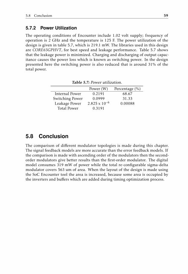
The operating conditions of Encounter include 1.02 volt supply; frequency ofoperation is 2 GHz and the temperature is 125 F. The power utilization of thedesign is given in table 5.7, which is 219.1 mW. The libraries used in this designare CORE65GPHVT, for best speed and leakage performance. Table 5.7 showsthat the leakage power is minimized. Charging and discharging of output capac-itance causes the power loss which is known as switching power. In the designpresented here the switching power is also reduced that is around 31% of thetotal power.
Table 5.7: Power utilization.
Power (W) Percentage (%)Internal Power 0.2191 68.67
Switching Power 0.0999 31.33Leakage Power 2.825 x 10⁻⁶ 0.00088
Total Power 0.3191
5.8 Conclusion
The comparison of different modulator topologies is made during this chapter.The signal feedback models are more accurate than the error feedback models. Ifthe comparison is made with ascending order of the modulators then the second-order modulators give better results than the first-order modulator. The digitalmodel consumes 319 mW of power while the total re-configurable sigma-deltamodulator covers 563 um of area. When the layout of the design is made usingthe SoC Encounter tool the area is increased, because some area is occupied bythe inverters and buffers which are added during timing optimization process.

Part VI
SoC Encounter Manual

6SoC Encounter Manual
6.1 Introduction
One aim of the thesis was to work on SoC Encounter to generate the layout. Thischapter presents a user manual for SoC Encounter, which can be considered asone of the product of this thesis work. This manual is only intended to be usedin Institutionen för Systemteknik (ISY) at Linköing University, as the file pathsmentioned in this manual are only intended for Linköping University’s server.
6.2 Behavioral Modeling (MODELSIM)
This section presents a step by step guide to design a digital model using vsim(MODELSIM).
Open MODELSIM using the command
module load mentor/modeltech10.0
vsim
Create a new project by “File→ New→ Project”.
Make sure the project is created in a new directory. If the directory is not presentthen create a new directory by
mkdir digRfDacSdm_Top
Better strategy is to work in a single directory, so that one can keep track of allthe designs. So create a new project in the directory which is already created.Modules and sub-modules can be created using Verilog/VHDL language; Verilog
63

64 6 SoC Encounter Manual
is used in this manual. Before continuing to the synthesis of the design; verifythe model using behavioral simulations in MODELSIM.
6.3 Synthesis and Netlist (Design Compiler)
In this section the design is synthesized and a netlist will be created using designcompiler. Design compiler can be launched by following instructions.
Open terminal window and go to project directory that is created for the Topmodel and create a new directory named “synopsys”, using
mkdir synopsys
Copy 2010.12 file to synopsys directory by
cp path_of_file_to_copy/2010.12 digRfDacSdm_Top/synopsys /
module use digRfDacSdm_Top
cd digRfDacSdm_Top
module load synopsys/2010.12
design_vision
When the compiler is launched the first and the most important task is to setupthe default libraries. The libraries can be chosen according to the requirementsof your design.
The GP libraries are considered to be the fastest ones as compared to the LP. Dif-ferent options are available for GP and LP like HVT, LVT and SVT. There aretradeoffs between all available libraries. LVT libraries give the best performancewith high speed applications; however the leakage is very high. Typically HVToption is considered to have the best tradeoff between speed vs. leakage, morediscussion has already been done in section 4.3 of chapter 4.
To setup libraries open “File→ Setup→ defaults”.
Remember to update the libraries according to the file extensions mentioned indefault field. The best libraries for high speed and low leakage are CORE65GPHVT.Select the following libraries from directory
/sw/cadence/libraries/cmos065RF_534_IC615.010/CORE65GPHVT_5.1/libs/
Select the libraries as
Link Library = CORE65GPHVT_bc_1.02V_125C.db
Target Library = CORE65GPHVT_bc_1.02V_125C.db
Symbol Library = CORE65GPHVT.sdb

6.3 Synthesis and Netlist (Design Compiler) 65
6.3.1 Analyze Design
Every RTL code is not necessarily synthesizable even if it has passed the behav-ioral simulations. This could happen because of using statements that do notmake any sense for synthesis or if some functions are used which are not synthe-sizable. So the better thing is to write a synthesizable code than using functions.
First task of synthesis is checking syntax of code. Analysis phase compiles andchecks whether the Verilog/VHDL designs are synthesizable or not.
Designs must be analyzed in ascending order; top design must be analyzed last.Up/down buttons can be used to arrange the designs in bottom-up order. UseFigure 6.1 as a reference; where the top most design is at the bottom, i.e., di-gRfDacSdm_BitSpliter.v. When the designs are loaded press OK to analyze themodules; this will also store design units in WORK directory.
Figure 6.1: Set-up design parameters for analysis.
Any warnings and errors will be displayed in console or log view. The warningor error messages contain detailed description of errors or warnings. Before con-tinuing all the errors should be removed otherwise no design will be loaded indesign compiler. It is better to remove all the warnings in design also as compilermay create some extra hardware or latches which are not desirable.
Analysis can be initialized from console terminal using command
analyze -library WORK -format Verilog/VHDL
Mention all Verilog files in top-down order, separated by a “space”.

66 6 SoC Encounter Manual
Table 6.1: Registers indicated by elaborate process.Register Name Type Width Bus MB AR AS SR SS STint_delay_in_reg Flip-Flop 4 Y N N N N N Nout_reg Flip-Flop 1 N N N N N N Nint_delayout_reg Flip-Flop 3 Y N N N N N Nint_delayout_reg Flip-Flop 4 Y N N N N N N
6.3.2 Elaborate Design
When the design is analyzed, a pre-synthesis of the analyzed design is required,which is performed in elaboration phase. Pre-synthesis is to identify all the reg-isters, flip-flops and gates; that are necessary to be used with the design. To runelaborate go to “File→ Elaborate”.
A window will pop-up where library, top design and parameters need to be spec-ified. Library will be set to default and the design field should select the top RTLdesign. If generic VHDL design is used then its generic ports’ parameters willappear in parameters field. By setting these parameters one can change the sizeof the design. If “Reanalyze out-of-date libraries” field is checked all the designfiles, which are modified after the analysis phase will be analyzed again.
The elaboration of design gives number of registers used in design that are dis-played in console window.
In “types” column of table 6.1, only flip-flops are mentioned no latches.
6.3.3 Linking Design
The design should be elaborated without any warnings of missing registers. Thismeans that any missing registers indicated by the design compiler, should not beused. If there are any registers then link the design to libraries according to thewarnings displayed in console.
The design can be linked using “File → Link Design” or through console usingequivalent command
set link_library "$link_library path_to_*.db_library"
link
After all the libraries (*.db), containing missing register definitions, are linkedthe warnings should be removed. If there are still warnings then modify thedesign or check the linked libraries.
6.3.4 Design Constraints
Timing and area are two basic constraints required by almost every design. Ifthe design is clocked then the timing constraints are set before compiling. Area

6.3 Synthesis and Netlist (Design Compiler) 67
constraints only define the minimum area that will be used while optimizing thedesign.
Figure 6.2: Symbol of top level design schematic for sigma-delta modulator.
To set timing constraints select top design model digrfDacSdm_BitSplitter fromlogical hierarchy window. Click “Create Schematic” icon to create a symbol ofyour design which will include all the input and output ports.
In design symbol click clock port and open “Attributes→ Specify Clock”. A win-dow will pop-up where clock name, period, rising and falling edges are required.Write clock name as specified in RTL design and specify a period of clock accord-ing to the maximum frequency at which the design will be working. Clock periodfield is defined in nano-seconds (in this manual); this time scale is defined in celllibraries. If design is to be operated at 2 GHz then specify 0.5 in period field.Then the rising and falling edges have to be setup to complete the clock specifica-tion. When the desired duty cycle is 50% then rising edge should be set to 0 andfalling edge should be at period/2. When the edges are setup, the portion belowthe edge specification field in figure 6.3 shows the clock which is specified by thesettings described above. It depends on the designer if he wants to have a dutycycle of 50% or not. It is also possible to set a variable duty cycle.
Timing constraints are the most important constraints of all, as without timingconstraints there will be problems of synchronization. When the timing con-straints are met the design compiler tries to optimize the area. To set the areaconstraints select the top cell in logical hierarchy window and open area con-straints window by “Attributes→ Optimization Constraints→ Design Constraints”
In figure 6.4 set “Max Area” field to zero which means that the design compilerwill try to use minimum area possible.
Equivalent commands to set timing and area constraints are
create_clock -name "clk" -period 0.5 -waveform 0 0.25 clk set_max_area 0
6.3.5 Compiling Design
After specifying all the design constraints now the Verilog design is translatedto a gate level netlist. Compilation phase translates the generic gates, defined inelaboration phase, in logic gates from standard cell libraries.

68 6 SoC Encounter Manual
Figure 6.3: Parameters set-up for clock specification.
Select the top design in logical hierarchy and open the compile window shown infigure 6.5 by “Design→ Compile Design’’.
In window popped-up un-check the “Exact Map” box and keep the default op-tions. Just click “OK” to run the compiler. Equivalent command to compile thedesign from console is
compile -map_effort medium -area_effort medium.
When synthesizing large designs use medium area and map effort as the largeeffort may cause large delays in synthesizing. Now the mapped schematic of anydesign can be viewed through schematic viewer. Click on any design in logicalhierarchy and click “Create Design Schematic” icon to view the schematic. Thedesign schematic is generated using standard cells defined in a netlist.
6.3.6 Design Reports
Different reports of the synthesized design can be generated in design compilerwhich are helpful to investigate the mapped design.
Different reports can be generated by selecting “Design” in top menu of designcompiler. The different reports available are “Report Constraints”, “Area Report”,“Critical Path Report” and “Resource Usage Report”. Reports related to timingcan be viewed by clicking “Timing” and then selecting a related report.

6.3 Synthesis and Netlist (Design Compiler) 69
Figure 6.4: Setting design constraints for design
6.3.7 Verilog Netlist File
In this step Verilog netlist file of mapped design is generated which contains thestandard cells information. This file can be used for post-synthesis simulationsand will also be the input of the SoC Encounter Tool. To save a Verilog netlist filejust click “File→ Save As” and save the file using *.v file extension.
Alternatively we can also save the netlist file using a command
write -format Verilog -hierarchy -output netlist_file_name.v
6.3.8 Timing and Design Constraints File
The synthesized netlist will be used for place and route. So we have to gener-ate SDF timing file and design constraints file for place and route tool (SoC En-counter). These files can be generate by using
write_sdf -version 2.1 file_name.sdf
write_sdc -nosplit file_name.sdc
A good practice is to save the design after each step which will be helpful inreloading the design at any desired stage. The design can be saved by “File →Save As” and saving the design as *.ddc file. The equivalent command to save thedesign is
write -hierarchy -format ddc -output outputfile_name.ddc

70 6 SoC Encounter Manual
Figure 6.5: Compile window parameters.
When it is desired to reload a saved design, use “File → Read”. The equivalentcommand to read the design is
read_file -format ddc file_to_read.ddc
This entire process will generate the netlist file of the top module, which is usedfor post-synthesis simulations and place and route. An SDF timing file and SDCfile containing design constraints for place and route will also be the outcome ofthis process. It also estimates the design’s dynamic and static power consumptionand required area for a design.
6.4 Cadence Encounter Manual
In this section all necessary steps are presented which are required to place androute the Verilog netlist using the place and route tool (SoC Encounter) from“Cadence Design Systems”. Cadence SoC Encounter can be instantiated by usingfollowing commands.
setenv LM_LICENSE_FILE [email protected]
setenv DD_DONT_DO_OS_LOCKS set
setenv PATH $PATH/sw/cadence/EDI101/tools/bin:/sw/cadence/EDI101/bin
xterm -e encounter &
When Encounter is launched two different windows appear, one is the GUI ofEncounter and the other is Encounter’s console. The main focus of this tutorialis to use Encounter with GUI but equivalent commands will also be presented.GUI is a better way to use Encounter for a new user, because one can visualize

6.4 Cadence Encounter Manual 71
Figu
re6.6:
Gat
ele
vels
chem
atic
of4-
bit
sigm
a-d
elta
mod
ula
tor.
72 6 SoC Encounter Manual
everything while designing. For more advanced users scripts are recommendedfor more precise and accurate designs.
The main window has three different design views; Floorplan, Amoeba and Phys-ical. Floorplan view displays the core area, power railings and the IO bound-ary. Global net connections are also displayed by the floorplan view. Amoebaview displays standard cell boundaries which are placed inside the core area. Byamoeba view one can visualize the physical placement of all the modules in adesign. Physical view displays all the standard cell blocks and interconnection ofthe blocks.
When Encounter is invoked, it creates two very useful files in current workingdirectory. One is “encounter.cmdx” which stores all the executed commands. Ifone is using GUI for designing, all the equivalent commands are also generatedand stored in the file. The second file is “encounter.logx”, which has all the loginformation of the current Encounter’s session.
Before continuing to import the design and routing stuff some files are preparedwhich have all definitions of standard cells (Library Exchange Format, LEF, files),clock buffers, inverters, Verilog netlist file, IO mapping file, timing informationfor the design to be imported and Timing Library Format (tlf) file.
The Verilog netlist file is generated in section 6.3 using design compiler. LEF filesare considered to be the most important as they have physical layout definitionsfor the standard cells used in design. The LEF files contain information aboutmetal and via layers and via generate rules [Systems [2003]]. These LEF filesprovide an abstract view of the layout and the tool doesn’t need to create thefull layout, it just creates the abstract layout. Order of LEF files, in which thesefiles are loaded, is very important. Encounter kit’s LEF file should be loadedfirst. Secondly CORE library file, which is used earlier in design compiler, willbe loaded. At the end, all other files which contain definitions of clock buffers,clock inverters and fillers should be loaded. Design constraints file (SDC) wasalso generated at the end of design synthesis in previous section. Timing libraryfile can be generated using syn2tlf tool from Synopsys.
Syn2tlf is a translator from Synopsys to Timing Library Format (TLF). Syn2tlfis used to translate the Synopsys library to TLF. This translator can also trans-late table_lookup, generic_cmos and cmos2 delay models to TLF’s table model[Synopsys [2005]]. One can generate the tlf file for the libraries used in synthesisprocess by running this command in terminal.
syn2tlf input_library_to_tlf_translator.lib
Library input_library_to_tlf_translator.lib is same library which was used to cre-ate the synthesized netlist of the design. In last section about generation of netlistfile, CORE65GPHVT_bc_1.02V_125C.db is used, so the same file will be used bytranslator. Figure 6.7 shows the data model (input and output) of the translator.Input file is a *.lib and the output is the corresponding *.tlf file. The data modelindicates that we have several options available for the translator. The above com-

6.4 Cadence Encounter Manual 73
mand is the simplest one to execute. Detailed information about how to use thesyn2tlf tool can be found in syn2tlf user guide [Synopsys [2005]].
Figure 6.7: Data model of syn2tlf.
When all the design files are ready then one can start importing design, powerplanning, placing standard cells and routing the design.
6.4.1 Importing Design
Importing of design includes specification of the files that is prepared in previoussection. When all the specification files are ready then these files can be saved ina configuration file. One can use this configuration file to load all the files usinga single command through console. The configuration file includes all the filescreated in section 6.2 and section 6.3.
Select “File→ Import Design”, which will open design import window as shownin figure 6.8. Fill out the design import form one by one. First select the Verilognetlist file which contains the design to be placed and routed. Click on browsebutton next to the LEF files’ field and select the required LEF files and remem-ber to select the LEF files in order as mentioned in section 4.2. If the LEF filesare loaded; then there is no need of loading OA reference Libraries, OA abstractView names and OA Layout view names. In “floorplan” section select the IO as-signment file, which contains information about how the pins will be mapped inthe design. It is possible to load the IO assignment file after the floor planningstep, as it will be easy at that point to decide the placement of pins. A sample IOfile is shown in appendix A.
Now click the “Advanced” tab and select “Power” and write the power names. Re-member that power pin names should be the same as were defined in Encounterkit’s technology file. Otherwise Encounter will not be able to connect the globalnets and route the power properly.

74 6 SoC Encounter Manual
Figure 6.8: Design import window with parameters to set-up to import de-sign in Encounter.
Save the configuration file by clicking save button and choosing a suitable name.Saving configuration file will save the time to go through above process all thetime. In future whenever it is required to import the same design just open the de-sign import window and load the saved configuration by clicking “Load” button.An example configuration file can be seen in appendix B.
You may have observed in this process that the design constraints (SDC) file andtiming library format (TLF) file is not loaded, because Encounter’s version 10.0does not have the option of loading the timing information files. To load the tim-ing files, edit the configuration file. Open configuration file in any available texteditor. Locate the property “set rda_Input(ui_timelib)” and write the *.tlf filein double quotes like "/bin/CORE65GPHVT_bc_110V_125C.tlf". Remember towrite complete path to the file if not located in current working directory. To loaddesign constraints (SDC) file locate the property “set rda_Input(ui_timingcon_file)”and fill quotes with SDC file name with complete path. After changing the config-uration file save the file and click OK in the design import window. The importeddesign in cadence will look like as shown in figure 6.9.
A good practice is to read the log file at each step as errors and unwanted warn-ings are hard to track later. Log can be read from Encounter’s console or from thefile “encounter.logx”, generated in current working directory.
This report also includes equivalent commands which are helpful in complete
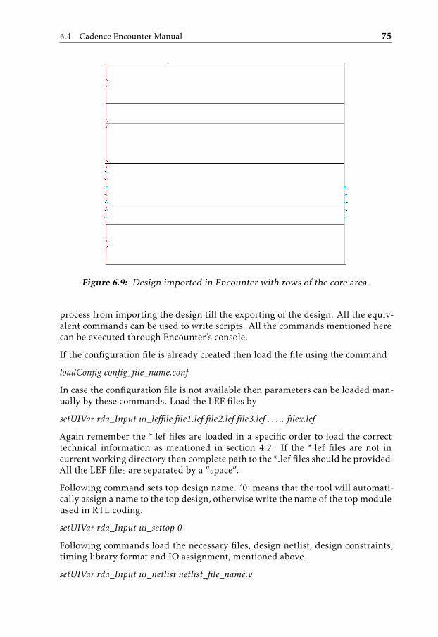
6.4 Cadence Encounter Manual 75
Figure 6.9: Design imported in Encounter with rows of the core area.
process from importing the design till the exporting of the design. All the equiv-alent commands can be used to write scripts. All the commands mentioned herecan be executed through Encounter’s console.
If the configuration file is already created then load the file using the command
loadConfig config_file_name.conf
In case the configuration file is not available then parameters can be loaded man-ually by these commands. Load the LEF files by
setUIVar rda_Input ui_leffile file1.lef file2.lef file3.lef . . . .. filex.lef
Again remember the *.lef files are loaded in a specific order to load the correcttechnical information as mentioned in section 4.2. If the *.lef files are not incurrent working directory then complete path to the *.lef files should be provided.All the LEF files are separated by a “space”.
Following command sets top design name. ‘0’ means that the tool will automati-cally assign a name to the top design, otherwise write the name of the top moduleused in RTL coding.
setUIVar rda_Input ui_settop 0
Following commands load the necessary files, design netlist, design constraints,timing library format and IO assignment, mentioned above.
setUIVar rda_Input ui_netlist netlist_file_name.v

76 6 SoC Encounter Manual
setUIVar rda_Input ui_timingcon_file design_constraints_file.sdc
setUIVar rda_Input ui_timelib timing_library_format_file.tlf
setUIVar rda_Input ui_io_file IO_assignment_file.io
After loading the configuration file or the parameters file, which will load thedesign, run the “commitConfig” to import the design.
Again the good practice is to save the design at each major step so that one canrestore the design in future from a desired step. The design can be saved by “File→ Save Design” or using this command in Encounter’s console.
saveDesign design_name_to_save.enc
A naming convention for saving is better choice which will later be helpful intracking stage of the design. After import we can save the design with nameincluding keyword import “design_name_to_save_import.enc”. The design canbe restored by “File→ Restore Design” and selecting the appropriate design needsto be restored.
6.4.2 Floor Planning the Design
Floor plan defines the actual size of the core used, number of rows that will beused by standard cells, area of power rings and distance of core to IO boundaries.Floor planning is also important as one can define the exact area of the chip usedby design. If the chip area is known then the floor planning is done according tothe limitations of the available area.
Open the floor planning window as shown in figure 6.10, by “Floorplan→ SpecifyFloorplan”.
Normally if chip area is not provided then the core area is set by selecting “Size”in “Design Dimensions”. Aspect ratio (H/W) is ratio between height (H) andwidth (W) of the core area. Aspect ratio ‘1’ means that area of core will be asquare and for a rectangle area choose ‘2’ in aspect ratio field. Core utilizationdefines the core area that will be used by the standard cell blocks defined inVerilog netlist.
Core utilization ‘1’ means that hundred percent core will be used by the blocks.That should not be the case as there should be some free space for power plan-ning. Timing optimization is the most critical part of the place and route whichmay also add inverters and buffers to remove the difference in clock delays be-tween different blocks. So the “Core Utilization” should be kept around 60 to 70percent.
While defining core to IO boundary, one thing should be kept in mind that powerrails will be added later, so leave some space for power rails in between core andIO boundary. When all the parameters are setup; click OK to get floorplan similarto figure 6.11.
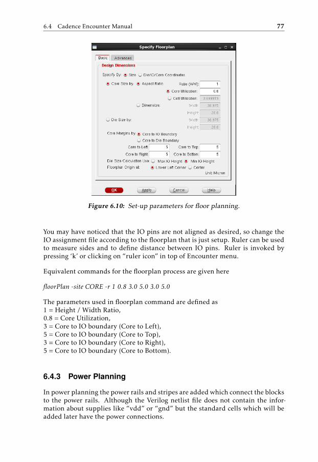
6.4 Cadence Encounter Manual 77
Figure 6.10: Set-up parameters for floor planning.
You may have noticed that the IO pins are not aligned as desired, so change theIO assignment file according to the floorplan that is just setup. Ruler can be usedto measure sides and to define distance between IO pins. Ruler is invoked bypressing ‘k’ or clicking on “ruler icon” in top of Encounter menu.
Equivalent commands for the floorplan process are given here
floorPlan -site CORE -r 1 0.8 3.0 5.0 3.0 5.0
The parameters used in floorplan command are defined as1 = Height / Width Ratio,0.8 = Core Utilization,3 = Core to IO boundary (Core to Left),5 = Core to IO boundary (Core to Top),3 = Core to IO boundary (Core to Right),5 = Core to IO boundary (Core to Bottom).
6.4.3 Power Planning
In power planning the power rails and stripes are added which connect the blocksto the power rails. Although the Verilog netlist file does not contain the infor-mation about supplies like “vdd” or “gnd” but the standard cells which will beadded later have the power connections.
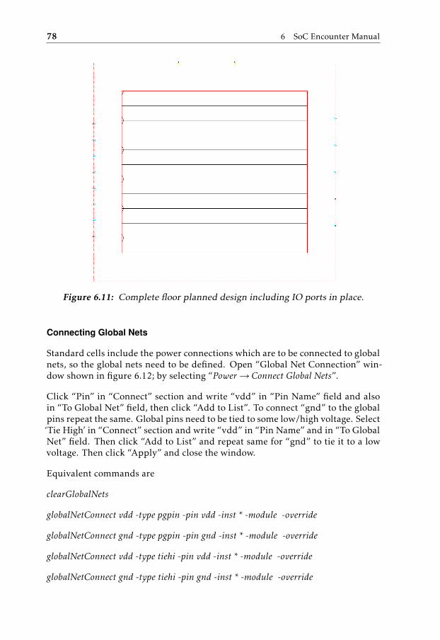
78 6 SoC Encounter Manual
Figure 6.11: Complete floor planned design including IO ports in place.
Connecting Global Nets
Standard cells include the power connections which are to be connected to globalnets, so the global nets need to be defined. Open “Global Net Connection” win-dow shown in figure 6.12; by selecting “Power→ Connect Global Nets”.
Click “Pin” in “Connect” section and write “vdd” in “Pin Name” field and alsoin “To Global Net” field, then click “Add to List”. To connect “gnd” to the globalpins repeat the same. Global pins need to be tied to some low/high voltage. Select‘Tie High’ in “Connect” section and write “vdd” in “Pin Name” and in “To GlobalNet” field. Then click “Add to List” and repeat same for “gnd” to tie it to a lowvoltage. Then click “Apply” and close the window.
Equivalent commands are
clearGlobalNets
globalNetConnect vdd -type pgpin -pin vdd -inst * -module -override
globalNetConnect gnd -type pgpin -pin gnd -inst * -module -override
globalNetConnect vdd -type tiehi -pin vdd -inst * -module -override
globalNetConnect gnd -type tiehi -pin gnd -inst * -module -override

6.4 Cadence Encounter Manual 79
Figure 6.12: Global net connection window.
Adding Power Rails
Power rails will be added around the core. These rails are used to connect thestripes which will be placed through the rows of the core. Open “Add Rings”window by “Power→ Power Planning→ Add Ring”.
Net field of figure 6.13 defines nets that will be added to the rails. In “Nets” fieldwrite “gnd” and “vdd” in order, as the first one will be the inner rail and thesecond will be the outer rail. Like if “gnd” and “vdd” are mentioned then theinner rail will be “gnd” and outer will be “vdd”.
In “Ring Configuration” area “Layer” field is used to define the layers used for allfour sides and which metal layers will be used; default options are good. “Width”filed defines the width of the power rails and the “Spacing” field defines distancebetween the power rails. If the “Offset” is set to “Centre in Channel”; this willplace the power rails between the core and IO boundary.
Click on advanced tab which will show up a window similar to figure 6.14a. Hereone can select sides on which the rails will be placed. If we want the rails to beplaced on each side then set the blocks according to figure 6.14a. This may notbe the best option to add rails in a design as this could cause the power issues forblocks placed in upper left or bottom left corner of the cores; so the better optionis to choose the extension on all sides of the core as shown in figure 6.14b. Thismeans that the power pins will be available on all sides of the core and all blockswill share equal power.
Click OK to generate the power rails according to the properties that were set
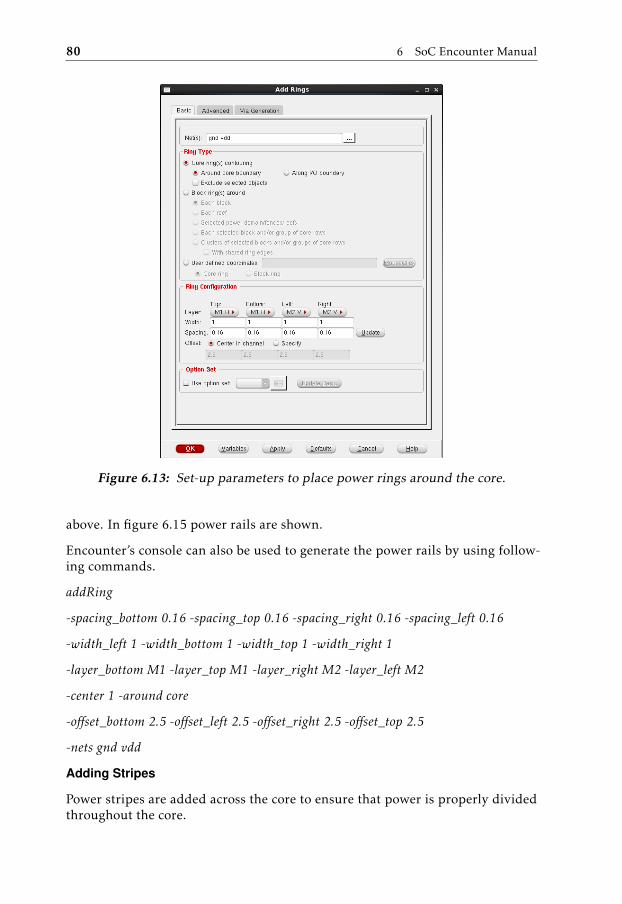
80 6 SoC Encounter Manual
Figure 6.13: Set-up parameters to place power rings around the core.
above. In figure 6.15 power rails are shown.
Encounter’s console can also be used to generate the power rails by using follow-ing commands.
addRing
-spacing_bottom 0.16 -spacing_top 0.16 -spacing_right 0.16 -spacing_left 0.16
-width_left 1 -width_bottom 1 -width_top 1 -width_right 1
-layer_bottom M1 -layer_top M1 -layer_right M2 -layer_left M2
-center 1 -around core
-offset_bottom 2.5 -offset_left 2.5 -offset_right 2.5 -offset_top 2.5
-nets gnd vdd
Adding Stripes
Power stripes are added across the core to ensure that power is properly dividedthroughout the core.

6.4 Cadence Encounter Manual 81
(a) (b)
Figure 6.14: Selecting power rails around the core. (a) Worst selection, (b)Best selection.
Before continuing to add the stripes, necessary thing is to understand orientationof the rows. In figure 6.16, observe that all the rows have straight line on one sideand on the other side there is a cut mark on left side. The straight indicates the“vdd” and the side with cut mark indicates “gnd”.
Open the “Add Stripes” window, as shown in figure 6.16, by “Power → PowerPlanning→ Add Stripe”. The better option is to add stripes one by one; first “vdd”and then “gnd”. So first select “vdd” in “Nets” field set width according to thedesign requirements. The spacing is selected according to the width of the blocksdefined in Encounter kit’s *.lef file. One can read the technology file to know theexact width of the blocks or can just measure the width of the rows. “Number ofsets” defines how many sets of “vdd” or “vss” will be added.
“Stripes Boundary” should be set to “Core Ring”, as all the stripes will be con-nected to the power rings around the core. Similarly place of first and last stripeis also defined in field “First/Last Stripe”. One can measure the relative distanceby the ruler to mention in this field. Click OK to generate the power stripessimilar to figure 6.17.
Equivalent commands required to generate the stripes are
addStripe
-max_same_layer_jog_length 6
-number_of_sets 6
-ybottom_offset -0.25 -ytop_offset -0.25
-spacing 2 -merge_stripes_value 2.5
-direction horizontal

82 6 SoC Encounter Manual
Figure 6.15: Design with added rails around the core.
-layer M1 -width 0.5
-nets vdd gnd
Remember both stripes, ‘vdd’ and ‘vss’, can be added at the same time or one byone, but the better option is to add them one after the other.
Routing Power Nets
Now when all the power nets are setup then power structure has to be routed.Click “Route → Special Route” to open the “SRoute” window. In figure 6.18uncheck the “Pad pins” and “Pad rings” and click Ok to route the power struc-ture.
Notice that here we have the option of limiting the routing layers. It is also pos-sible that the power routing is done using Encounter’s console. Equivalent com-mands used for the power routing are;
sroute
-connect blockPin corePin floatingStripe
-blockPin useLef
-layerChangeRange M1 M4
-nets gnd vdd
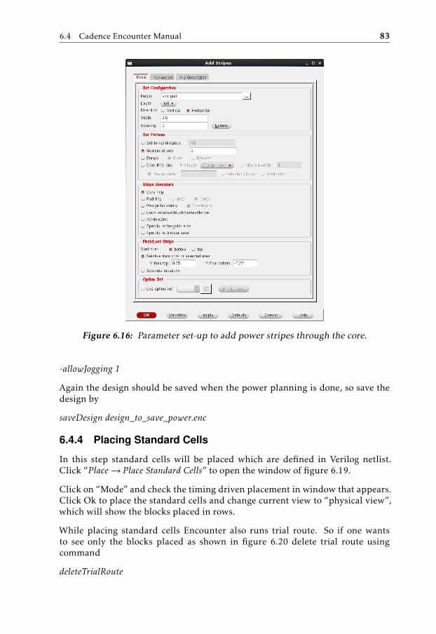
6.4 Cadence Encounter Manual 83
Figure 6.16: Parameter set-up to add power stripes through the core.
-allowJogging 1
Again the design should be saved when the power planning is done, so save thedesign by
saveDesign design_to_save_power.enc
6.4.4 Placing Standard Cells
In this step standard cells will be placed which are defined in Verilog netlist.Click “Place→ Place Standard Cells” to open the window of figure 6.19.
Click on “Mode” and check the timing driven placement in window that appears.Click Ok to place the standard cells and change current view to “physical view”,which will show the blocks placed in rows.
While placing standard cells Encounter also runs trial route. So if one wantsto see only the blocks placed as shown in figure 6.20 delete trial route usingcommand
deleteTrialRoute
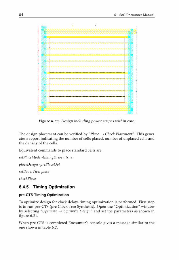
84 6 SoC Encounter Manual
Figure 6.17: Design including power stripes within core.
The design placement can be verified by “Place→ Check Placement”. This gener-ates a report indicating the number of cells placed, number of unplaced cells andthe density of the cells.
Equivalent commands to place standard cells are
setPlaceMode -timingDriven true
placeDesign -prePlaceOpt
setDrawView place
checkPlace
6.4.5 Timing Optimization
pre-CTS Timing Optimization
To optimize design for clock delays timing optimization is performed. First stepis to run pre-CTS (pre Clock Tree Synthesis). Open the “Optimization” windowby selecting “Optimize → Optimize Design” and set the parameters as shown infigure 6.21.
When pre-CTS is completed Encounter’s console gives a message similar to theone shown in table 6.2.

6.4 Cadence Encounter Manual 85
Figure 6.18: SRoute window to route power nets.
Figure 6.19: Placing standard cells in design.
Slack of critical path in design is given by worst negative slack (WNS). If thevalue of the slack is negative then the timing constraints are not met and positivevalue means that the timing constraints are already met. During pre-CTS somestandard cells may be replaced by newer ones to meet the timing constraints;which may result in an increase or a decrease in density of the core.
Equivalent command to perform pre-CTS is
optDesign -preCTS -outDir file_name_to_save_pre_CTS_report
Clock Tree Synthesis
When the tool places the standard cells it does not take into account the clockroute. So the delay in clock phase for different cells is not constant which mayresult in a faulty chip. So we need to perform clock tree synthesis.
Clock tree synthesis needs a “tree specification file” which contains information
Table 6.2: Summary of optimized design after pre-CTSSetup mode all reg2reg in2reg
WNS (ns) 0.093 0.093 0.106TNS (ns) 0.000 0.000 0.000Violating Paths 0 0 0All Paths 16 12 16Density 72.339%Routing Overflow 0.00% and 0.00% V

86 6 SoC Encounter Manual
Figure 6.20: Core area with standard cells placed.
about the tree synthesis. If you don’t have “tree specification file”, then use En-counter to create a sample specification file. This sample file can be edited lateraccordingly, for newer design requirements. A sample “tree specification file” islisted in appendix C.
Click “Clock → Synthesize Clock Tree” in main menu of Encounter window. Togenerate new “tree specification file” click on “Gen Spec. . . ” in basic tab of fig-ure 6.22.
This will open a window which has an option of selecting the clock buffers andinverters which will be placed during clock tree synthesis. Select all availableclock buffers and inverter from “Cells List” and add them to “Selected Cells” listby clicking add button.
In “Output Specification file” field write the name of the specification file. Com-pare settings with figure 6.23 and click OK to generate the specification file. Thecontrol returns to the window of figure 6.22; verify that the file selected in filefield is the same as the one just generated. Click OK to run clock tree synthesis.
Equivalent commands to run CTS from console are
createClockTreeSpec -output cts_file_name.cts
-bufferList add buffers and inverters separated by a “space”.
For example:
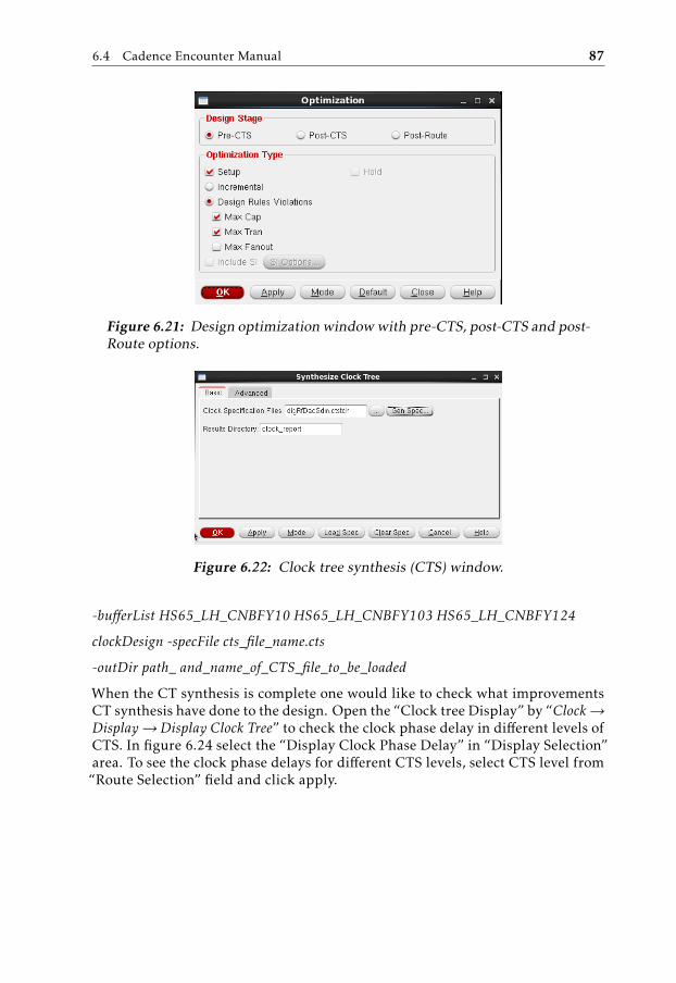
6.4 Cadence Encounter Manual 87
Figure 6.21: Design optimization window with pre-CTS, post-CTS and post-Route options.
Figure 6.22: Clock tree synthesis (CTS) window.
-bufferList HS65_LH_CNBFY10 HS65_LH_CNBFY103 HS65_LH_CNBFY124
clockDesign -specFile cts_file_name.cts
-outDir path_ and_name_of_CTS_file_to_be_loaded
When the CT synthesis is complete one would like to check what improvementsCT synthesis have done to the design. Open the “Clock tree Display” by “Clock→Display→ Display Clock Tree” to check the clock phase delay in different levels ofCTS. In figure 6.24 select the “Display Clock Phase Delay” in “Display Selection”area. To see the clock phase delays for different CTS levels, select CTS level from“Route Selection” field and click apply.
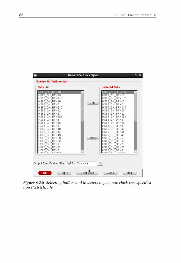
88 6 SoC Encounter Manual
Figure 6.23: Selecting buffers and inverters to generate clock tree specifica-tion (*.ctstch) file.
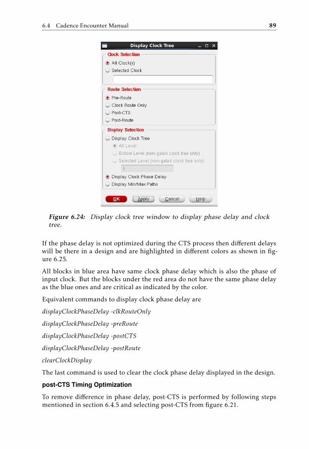
6.4 Cadence Encounter Manual 89
Figure 6.24: Display clock tree window to display phase delay and clocktree.
If the phase delay is not optimized during the CTS process then different delayswill be there in a design and are highlighted in different colors as shown in fig-ure 6.25.
All blocks in blue area have same clock phase delay which is also the phase ofinput clock. But the blocks under the red area do not have the same phase delayas the blue ones and are critical as indicated by the color.
Equivalent commands to display clock phase delay are
displayClockPhaseDelay -clkRouteOnly
displayClockPhaseDelay -preRoute
displayClockPhaseDelay -postCTS
displayClockPhaseDelay -postRoute
clearClockDisplay
The last command is used to clear the clock phase delay displayed in the design.
post-CTS Timing Optimization
To remove difference in phase delay, post-CTS is performed by following stepsmentioned in section 6.4.5 and selecting post-CTS from figure 6.21.
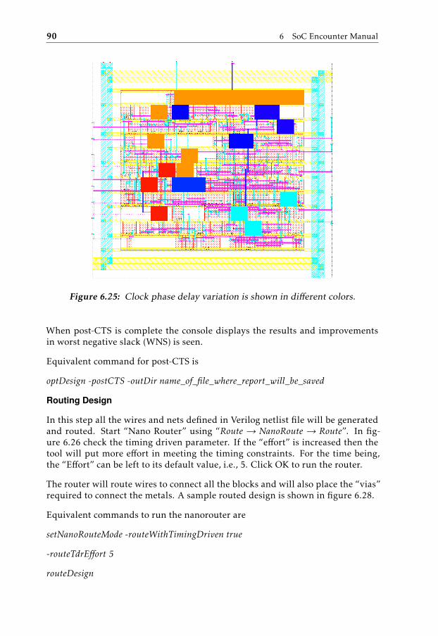
90 6 SoC Encounter Manual
Figure 6.25: Clock phase delay variation is shown in different colors.
When post-CTS is complete the console displays the results and improvementsin worst negative slack (WNS) is seen.
Equivalent command for post-CTS is
optDesign -postCTS -outDir name_of_file_where_report_will_be_saved
Routing Design
In this step all the wires and nets defined in Verilog netlist file will be generatedand routed. Start “Nano Router” using “Route → NanoRoute → Route”. In fig-ure 6.26 check the timing driven parameter. If the “effort” is increased then thetool will put more effort in meeting the timing constraints. For the time being,the “Effort” can be left to its default value, i.e., 5. Click OK to run the router.
The router will route wires to connect all the blocks and will also place the “vias”required to connect the metals. A sample routed design is shown in figure 6.28.
Equivalent commands to run the nanorouter are
setNanoRouteMode -routeWithTimingDriven true
-routeTdrEffort 5
routeDesign
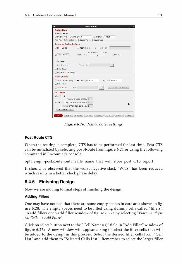
6.4 Cadence Encounter Manual 91
Figure 6.26: Nano router settings.
Post Route CTS
When the routing is complete; CTS has to be performed for last time. Post-CTScan be initialized by selecting post-Route from figure 6.21 or using the followingcommand in Encounter’s console.
optDesign -postRoute -outDir file_name_that_will_store_post_CTS_report
It should be observed that the worst negative slack “WNS” has been reducedwhich results in a better clock phase delay.
6.4.6 Finishing Design
Now we are moving to final steps of finishing the design.
Adding Fillers
One may have noticed that there are some empty spaces in core area shown in fig-ure 6.28. The empty spaces need to be filled using dummy cells called “fillers”.To add fillers open add filler window of figure 6.27a by selecting “Place→ Physi-cal Cells→ Add Filler”.
Click on select button next to the “Cell Names(s)” field in “Add Filler” window offigure 6.27a. A new window will appear asking to select the filler cells that willbe added to the design in this process. Select the desired filler cells from “CellList” and add them to “Selected Cells List”. Remember to select the larger filler
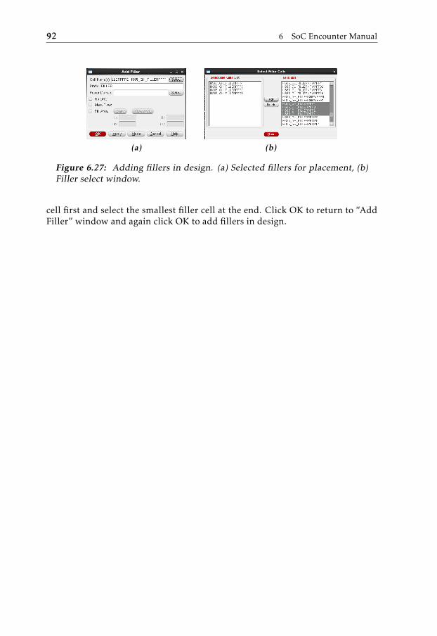
92 6 SoC Encounter Manual
(a) (b)
Figure 6.27: Adding fillers in design. (a) Selected fillers for placement, (b)Filler select window.
cell first and select the smallest filler cell at the end. Click OK to return to “AddFiller” window and again click OK to add fillers in design.
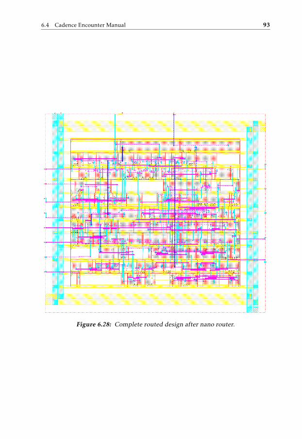
6.4 Cadence Encounter Manual 93
Figure 6.28: Complete routed design after nano router.

94 6 SoC Encounter Manual
Figure 6.29: Complete design with place & routed and empty spaces filled.
One can see that all the empty spaces in figure 6.29 will be filled with filler cells.Equivalent commands to add fillers using Encounter’s console are
addFiller
-cell All filler cells that will be added will be listed here separated by a space
-prefix FILLER
6.4.7 Checking Design
At this point, the design is ready to be exported to a gds file but before the designis exported a verification of design should be performed. There are several waysin which the design can be verified.
Verify Geometry
In this step, geometry of the design is verified. Figure 6.30 shows the optionsavailable to verify.
Here different options are available like minimum width of metals, minimumspacing between metals, short circuits, minimum cut and via enclosure etc. Selectthe options to be verified and click OK. In figure 6.30 the most common optionsare selected which are verified here. Warnings and errors will be marked by whitebox in design. Console results in
******** Start: VERIFY CONNECTIVITY ********
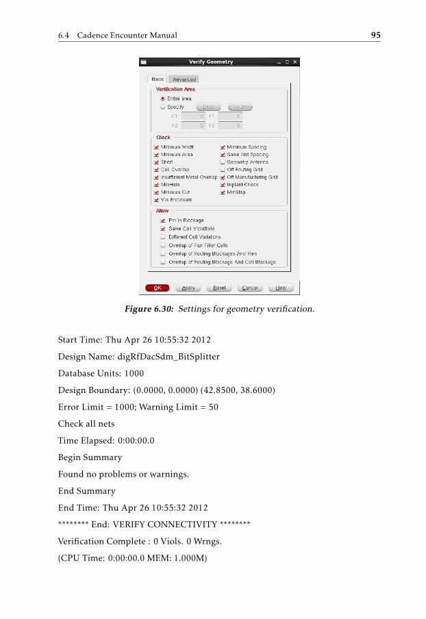
6.4 Cadence Encounter Manual 95
Figure 6.30: Settings for geometry verification.
Start Time: Thu Apr 26 10:55:32 2012
Design Name: digRfDacSdm_BitSplitter
Database Units: 1000
Design Boundary: (0.0000, 0.0000) (42.8500, 38.6000)
Error Limit = 1000; Warning Limit = 50
Check all nets
Time Elapsed: 0:00:00.0
Begin Summary
Found no problems or warnings.
End Summary
End Time: Thu Apr 26 10:55:32 2012
******** End: VERIFY CONNECTIVITY ********
Verification Complete : 0 Viols. 0 Wrngs.
(CPU Time: 0:00:00.0 MEM: 1.000M)

96 6 SoC Encounter Manual
If one wants to have a detailed look into the warnings and errors then open viola-tion browser from “Tools→ Violation Browser”. In violation browser all violationsare categorized according to the nature of the violation. Violation browser can beused to point a specific violation in layout window.
Equivalent command to verify the geometry is
verifyConnectivity -type all -report name_of_geometry_violation_report.rpt
Verify Connectivity
This step makes sure that all the modules/blocks are connected properly. Openfigure 6.31 by selecting “Verify→ Verify Connectivity” in main menu. Select thedefault options which are selected in figure 6.31.
Figure 6.31: Verifying connectivity of design.
A summary of violations will be displayed in console. Equivalent command ofconnectivity verification is
verifyConnectivity -type all -error 1000 -warning 50
Check DRC
Before exporting the design to a GDS file, the DRC should be checked using thefollowing command in Encounter terminal.
checkDrc
DRC errors in the design will be highlighted in physical window.

6.4 Cadence Encounter Manual 97
6.4.8 Export Design
Here design can be exported in several formats like gds file, Verilog netlist designand the SDF timing file.
Export GDS File
GDS file can be exported by opening GDS export window from “File→ Save→GDS/OASIS”. Set all the fields as shown in figure 6.32.
Figure 6.32: Export design to a *.gds file.
Map file field is important, because the design will be mapped to the technology,i.e., cmos065. So the map file should be chosen from the directory, where thestandard cell libraries were placed. Like in section 6.3 standard cell librarieswere chosen from the path
/sw/cadence/libraries/cmos065RF_534_IC615.010/CORE65GPHVT_5.1/libs/
In “libs” folder there is a *.map file; use this map file in “Map File” field to mapthe design to the desired technology library. Clicking OK will generate the *.gdsfile.
Design can be exported to gds file using the following commands.
streamOut output_gds_file_name.gds
-mapFile path_and_file_name_if_not_in_current_directory.map
-libName Library_name_in_which_design_is_imported_in_cadence
-units 1000 -mode ALL
The parameters used in streamout command area are
Output .gds file = output_gds_file_name.gds,
Output map file = path_and_file_name_if_not_in_current_directory.map,
Library Name = Library_name_in_which_design_is_imported_in_cadence,
98 6 SoC Encounter Manual
Units = 1000 (100, 200, 1000, 2000, 10000, 20000),
Mode = ALL (ALL, FILLONLY, NOFILL, NOINSTANCES).
Export Placed and Routed Net-list
During CTS process some buffers and inverters were added in design to overcomethe phase delay. Fillers were also added to fill the empty spaces in design. Thismeans that the new design has some extra design cells than the one which wasimported initially. To save the place and routed netlist file including all fillersand clock buffers and inverters, select “File → Save → Netlist” and uncheck the“Include Leaf Cell Definition”. Click ‘OK’ to save the netlist.
Equivalent command to run from console is
saveNetlist -excludeLeafCell name_of_palce_and_routed_netlist.v
Export SDF Timing File
To generate the SDF timing file open “Timing → Write SDF” from main menu.Uncheck the “Ideal Clock” field and click OK to generate the SDF timing file.
Following command can be used to generate SDF timing file from Encounterconsole.
write_sdf SDF_file_name.sdf
6.5 Import Design Netlist in Cadence
The design netlist can be imported to cadence environment to simulate the schematiclevel design. Import the design using the following steps.
1 Open cadence virtuoso window.
2 Select File -> Import -> Netlist.
3 Fill out the “Verilog In” window as shown in figure 6.33.
4 Click OK to import schematic in cadence.
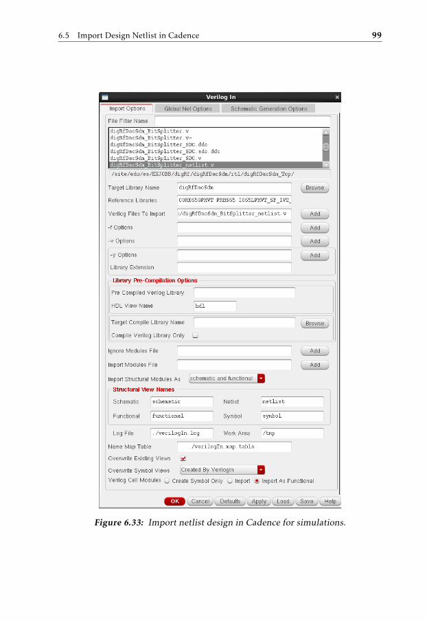
6.5 Import Design Netlist in Cadence 99
Figure 6.33: Import netlist design in Cadence for simulations.


Part VII
Conclusion and Future Work

7Conclusion and Future Work
The goal of the thesis was to design an all digital re-configurable sigma-deltamodulator.
The project was divided in sub modules to make things simpler during the projectphase. Different typologies of the sigma-delta modulators like signal feedbackand error feedback models were verified in MATLAB. The signal feedback modelprovides best performance in terms of SNR as compared to error feedback model.Modulators are also tested for different order of quantization levels; like first-order and second-order modulators. First-order modulators are quite same inperformance but the second-order modulators are different.
The second part of the thesis was to implement sigma-delta modulator in digitaldomain using SoC Encounter. On the basis of the simulation results that werecarried out in MATLAB, signal feedback modulator is the appropriate choice tomodel it using Verilog-HDL language for the hardware implementation. Themodulators were designed in 65-nm technology and re-configurability of themodulator is designed using MODELSIM.
Designing a chip through SoC Encounter is less time consuming as compared tomanual layout design methods, so saving time saves money, through this aspectdesigned chip would be cost efficient. One of the other advantages of the re-configurable sigma-delta modulator is that by changing input word-length of thesigma-delta modulator will automatically adjust itself through different switchesto meet the required specifications. The disadvantage of using SoC Encounter isthe chip area which is increased when an automatic layout is generated.
In the future one can work on power planning of the chip. The addition ofpipeline adders are suggested when the word-length is increased.
103


AIO Assignment File
Cadence Design Systems, Inc.
Cadence(R) Encounter(TM) IO Assignments
========================================
Version: 2
Offset: 9.75
Pin: out[0] E 2 0.180 0.180
Offset: 14.5
Pin: out[1] E 2 0.180 0.180
Offset: 19.25
Pin: out[2] E 2 0.180 0.180
Offset: 24
Pin: out[3] E 2 0.180 0.180
Offset: 28.75
Pin: out[4] E 2 0.180 0.180
Offset: 7.85
Pin: in[0] W 2 0.180 0.180
Offset: 10.7
Pin: in[1] W 2 0.180 0.180
105
106 A IO Assignment File
Offset: 13.55
Pin: in[2] W 2 0.180 0.180
Offset: 16.4
Pin: in[3] W 2 0.180 0.180
Offset: 19.25
Pin: in[4] W 2 0.180 0.180
Offset: 22.1
Pin: in[5] W 2 0.180 0.180
Offset: 24.95
Pin: in[6] W 2 0.180 0.180
Offset: 27.8
Pin: in[7] W 2 0.180 0.180
Offset: 15
Pin: reset N 1 0.180 0.180
Offset: 25
Pin: clk N 1 0.180 0.180
BConfiguration File
Generated by: Cadence Encounter 10.10-p003_1
OS: Linux x86_64(Host ID sob-00.edu.isy.liu.se)
Generated on: Mon Apr 16 11:51:38 2012
Design:
global rda_Input
set cwd path_of_current_working_directory.
set rda_Input(import_mode) -treatUndefinedCellAsBbox 0 -keepEmptyModule1
set rda_Input(ui_netlist) "digRfDacSdm_Integrator_netlist_GPHVT.v"
set rda_Input(ui_netlisttype) Verilog
set rda_Input(ui_rtllist) ""
set rda_Input(ui_ilmdir) ""
set rda_Input(ui_ilmlist) ""
set rda_Input(ui_ilmspef) ""
set rda_Input(ui_fmdir)
set rda_Input(ui_settop) 0
set rda_Input(ui_topcell)
set rda_Input(ui_celllib) ""
107
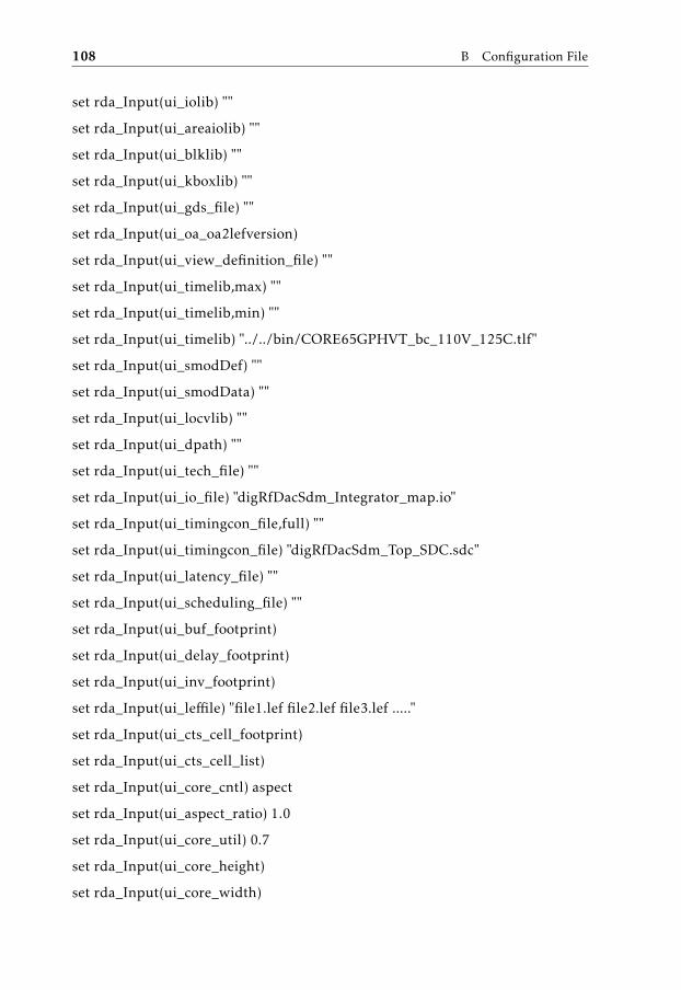
108 B Configuration File
set rda_Input(ui_iolib) ""
set rda_Input(ui_areaiolib) ""
set rda_Input(ui_blklib) ""
set rda_Input(ui_kboxlib) ""
set rda_Input(ui_gds_file) ""
set rda_Input(ui_oa_oa2lefversion)
set rda_Input(ui_view_definition_file) ""
set rda_Input(ui_timelib,max) ""
set rda_Input(ui_timelib,min) ""
set rda_Input(ui_timelib) "../../bin/CORE65GPHVT_bc_110V_125C.tlf"
set rda_Input(ui_smodDef) ""
set rda_Input(ui_smodData) ""
set rda_Input(ui_locvlib) ""
set rda_Input(ui_dpath) ""
set rda_Input(ui_tech_file) ""
set rda_Input(ui_io_file) "digRfDacSdm_Integrator_map.io"
set rda_Input(ui_timingcon_file,full) ""
set rda_Input(ui_timingcon_file) "digRfDacSdm_Top_SDC.sdc"
set rda_Input(ui_latency_file) ""
set rda_Input(ui_scheduling_file) ""
set rda_Input(ui_buf_footprint)
set rda_Input(ui_delay_footprint)
set rda_Input(ui_inv_footprint)
set rda_Input(ui_leffile) "file1.lef file2.lef file3.lef ....."
set rda_Input(ui_cts_cell_footprint)
set rda_Input(ui_cts_cell_list)
set rda_Input(ui_core_cntl) aspect
set rda_Input(ui_aspect_ratio) 1.0
set rda_Input(ui_core_util) 0.7
set rda_Input(ui_core_height)
set rda_Input(ui_core_width)

109
set rda_Input(ui_core_to_left) 0
set rda_Input(ui_core_to_right) 0
set rda_Input(ui_core_to_top) 0
set rda_Input(ui_core_to_bottom) 0
set rda_Input(ui_max_io_height) 0
set rda_Input(ui_row_height)
set rda_Input(ui_isHorTrackHalfPitch) 0
set rda_Input(ui_isVerTrackHalfPitch) 1
set rda_Input(ui_ioOri) R0
set rda_Input(ui_isOrigCenter) 0
set rda_Input(ui_isVerticalRow) 0
set rda_Input(ui_exc_net) ""
set rda_Input(ui_delay_limit) 1000
set rda_Input(ui_net_delay) 1000.0ps
set rda_Input(ui_net_load) 0.5pf
set rda_Input(ui_in_tran_delay) 0.1ps
set rda_Input(ui_captbl_file) ""
set rda_Input(ui_preRoute_cap) 1
set rda_Input(ui_postRoute_cap) 1
set rda_Input(ui_postRoute_xcap) 1
set rda_Input(ui_preRoute_res) 1
set rda_Input(ui_postRoute_res) 1
set rda_Input(ui_shr_scale) 1.0
set rda_Input(ui_rel_c_thresh) 0.03
set rda_Input(ui_tot_c_thresh) 5.0
set rda_Input(ui_cpl_c_thresh) 3.0
set rda_Input(ui_time_unit) none
set rda_Input(ui_cap_unit)
set rda_Input(ui_oa_reflib)
set rda_Input(ui_oa_abstractname)
set rda_Input(ui_oa_layoutname)

110 B Configuration File
set rda_Input(ui_sigstormlib) ""
set rda_Input(ui_cdb_file,min) ""
set rda_Input(ui_cdb_file,max) ""
set rda_Input(ui_cdb_file) ""
set rda_Input(ui_xtwf_file) ""
set rda_Input(ui_qxtech_file) ""
set rda_Input(ui_qxlayermap_file) ""
set rda_Input(ui_qxlib_file) ""
set rda_Input(ui_qxconf_file) ""
set rda_Input(ui_pwrnet) vdd
set rda_Input(ui_gndnet) gnd
set rda_Input(flip_first) 1
set rda_Input(double_back) 1
set rda_Input(assign_buffer) 1
set rda_Input(use_io_row_flow) 0
set rda_Input(ui_pg_connections) ""
set rda_Input(ui_gen_footprint) 0
CClock Tree Synthesis File
- Generated by: Cadence Encounter 10.10-p003_1- OS: Linux x86_64(Host ID sob-00.edu.isy.liu.se)- Generated on: Thu Apr 26 10:43:43 2012- Design: digRfDacSdm_BitSplitter- Command: clockDesign -genSpecOnly digRfDacSdm.ctstch
- Encounter(R) Clock Synthesis Technology File Format
– MacroModel –-MacroModel pin <pin> <maxRiseDelay> <minRiseDelay><maxFallDelay> <minFallDelay> <inputCap>
– Special Route Type –-RouteTypeName specialRoute-TopPreferredLayer 4-BottomPreferredLayer 3-PreferredExtraSpace 1-End
– Regular Route Type –-RouteTypeName regularRoute-TopPreferredLayer 4-BottomPreferredLayer 3-PreferredExtraSpace 1
111
112 C Clock Tree Synthesis File
-End
– Clock Group –-ClkGroup-+ <clockName>
————————————————————Clock Root : clkClock Name : clkClock Period : 0.5ns————————————————————AutoCTSRootPin clkPeriod 0.5nsMaxDelay 0.01ns - sdc driven defaultMinDelay 0ns - sdc driven defaultMaxSkew 20ps - sdc driven defaultSinkMaxTran 200ps - sdc driven defaultBufMaxTran 200ps - sdc driven defaultBuffer HS65_GH_BFX106 HS65_GH_BFX13 HS65_GH_BFX142HS65_GH_BFX18 HS65_GH_BFX2 HS65_GH_BFX213 HS65_GH_BFX22HS65_GH_BFX27 HS65_GH_BFX284 HS65_GH_BFX31 HS65_GH_BFX35HS65_GH_BFX4 HS65_GH_BFX40 HS65_GH_BFX44 HS65_GH_BFX49HS65_GH_BFX53 HS65_GH_BFX62 HS65_GH_BFX7 HS65_GH_BFX71HS65_GH_BFX9 HS65_GH_IVX106 HS65_GH_IVX13 HS65_GH_IVX142NoGating NODetailReport YESSetDPinAsSync NOSetIoPinAsSync NOSetASyncSRPinAsSync NOSetTriStEnPinAsSync NOSetBBoxPinAsSync NORouteClkNet YESPostOpt YESOptAddBuffer YESRouteType specialRouteLeafRouteType regularRouteEND

Bibliography
Wikner J.J. Afzal N. Study of modified noise-shaper architectures for oversam-pled sigma-delta dacs. NORCHIP, 2010, pages 1–4, 2010. Cited on page 24.
Kennedy M.P. Bhansali P., Hosseini K. Performance analysis of low power highspeed pipelined adders for digital sigma delta modulators. Electronic Letters,42(25):1442–1444, 2006. Cited on page 38.
A.R Duggal. Calibration of delta-sigma data converters in synchronous demod-ulation sensing applications. IEEE Sensors, Journal, 11(1):16–22, 2011. Notcited.
Van Roermund A. Janssen E. Look-Ahead Based Sigma-Delta Modulation. AnalogCircuits and Signal Processing. Springer, 2011. ISBN 9789400713864. URLhttp://books.google.se/books?id=HJtrNwXKk6IC. Cited on page 12.
David Jarman. A brief introduction to sigma delta conversion. 1995. Cited onpage 4.
Chen-Yi Lee Jui-Yuan Yu, Wan-Chun Liao. A mt-cdma based wireless body areanetwork for ubiquitous healthcare monitoring. Biomedical Circuits and Sys-tems Conference, 2006., pages 98–101, 2006. Cited on page 32.
Marcus Lovgren. Design of sigma delta modulators for oversampling digital toanalog converters. 2001. Cited on page 14.
Per Lowenborg. Mixed-Signal Processing Systems. 2nd edition, 2006. Cited onpage 23.
Bonizzoni E. Maloberti F. Noli S., Perez A.P. Sigma delta time interleaved currentsteering dac with dynamic elements matching. 52nd IEEE International Mid-west Symposium on Circuits and Systems, 2009. MWSCAS ’09, 2009. Cited onpage 32.
Jan Van der Spiegel Pervez M. Aziz, Henrik V. Sorensen. An overview of sigma-delta converters: How a 1-bit adc achieves more than 16-bit resolution. IEEESignal Processing Magazine, 13(1):61–84, 1996. Cited on page 15.
113

114 Bibliography
Murali S. Atienza D. De Micheli G. Benini L. Pullini. A, Angiolini F. Bringingnocs to 65 nm. IEEE Micro, 27(5):75–85, 2007. Cited on page 31.
Synopsys. SYN2TLF User Guide. 2005. Cited on pages 72 and 73.
Cadence Systems. LEF / DEF Language Reference Manual. 5.4 edition, 2003.Cited on page 72.
Upphovsrätt
Detta dokument hålls tillgängligt på Internet — eller dess framtida ersättare —under 25 år från publiceringsdatum under förutsättning att inga extraordinäraomständigheter uppstår.
Tillgång till dokumentet innebär tillstånd för var och en att läsa, ladda ner,skriva ut enstaka kopior för enskilt bruk och att använda det oförändrat för icke-kommersiell forskning och för undervisning. Överföring av upphovsrätten viden senare tidpunkt kan inte upphäva detta tillstånd. All annan användning avdokumentet kräver upphovsmannens medgivande. För att garantera äktheten,säkerheten och tillgängligheten finns det lösningar av teknisk och administrativart.
Upphovsmannens ideella rätt innefattar rätt att bli nämnd som upphovsmani den omfattning som god sed kräver vid användning av dokumentet på ovanbeskrivna sätt samt skydd mot att dokumentet ändras eller presenteras i sådanform eller i sådant sammanhang som är kränkande för upphovsmannens litteräraeller konstnärliga anseende eller egenart.
För ytterligare information om Linköping University Electronic Press se förla-gets hemsida http://www.ep.liu.se/
Copyright
The publishers will keep this document online on the Internet — or its possi-ble replacement — for a period of 25 years from the date of publication barringexceptional circumstances.
The online availability of the document implies a permanent permission foranyone to read, to download, to print out single copies for his/her own use andto use it unchanged for any non-commercial research and educational purpose.Subsequent transfers of copyright cannot revoke this permission. All other usesof the document are conditional on the consent of the copyright owner. Thepublisher has taken technical and administrative measures to assure authenticity,security and accessibility.
According to intellectual property law the author has the right to be men-tioned when his/her work is accessed as described above and to be protectedagainst infringement.
For additional information about the Linköping University Electronic Pressand its procedures for publication and for assurance of document integrity, pleaserefer to its www home page: http://www.ep.liu.se/
© Sohaib A. Qazi and S. Asmat Ali Shah