split non-linear cyclic analog-to-digital converter · split non-linear cyclic analog-to-digital...
TRANSCRIPT

Split Non-Linear Cyclic Analog-to-Digital Converter
By Shant Orchanian
The design, layout and simulation of a Cyclic ADC in the 0.18μm process that is fully
differential, self-calibrating and performs 1 million samples per second.
A Thesis
Submitted to the Faculty of
WORCESTER POLYTECHNIC INSTITUTE in partial fulfillment of the requirements for the
Degree of Master of Science in
Electrical and Computer Engineering
by
Shant Orchanian
April 2010
APPROVED:
______________________________________________________________________________ Professor John A. McNeill, Major Advisor ______________________________________________________________________________ Professor Stephen J. Bitar ______________________________________________________________________________ Professor Donald R. Brown

2
ABSTRACT
Analog-to-Digital Converters (ADC’s) are inherently optimized for linearity in order to produce an
accurate digital representation of an analog voltage. The Cyclic ADC’s linearity is limited by one of
its components, the residue amplifier. The residue amplifier is used to amplify the error between
the analog voltage and the digital decision by a gain of two in each cycle of a conversion. In previous
designs, this was accomplished by using a compound op-amp with a large open loop gain for
linearity, and negative feedback to achieve the gain of two. This thesis explores the use of a
resistively loaded differential pair to achieve this gain. The design reduces die size, power usage,
and analog complexity. To correct for this inherent non-linearity, a Split ADC concept is employed
to enable digital background calibration and a correction algorithm to account for this non-
linearity. The Integrated circuit is designed, laid out, and simulated using the Cadence Integrated
Circuit Front to Back design suite (ICFB) in the 0.18um Jazz CMOS process.

3
TABLE OF CONTENTS 1 Introduction ..................................................................................................................................................................... 8
1.1 Goals and Specifications .................................................................................................................................... 8
1.2 Project Motivation ............................................................................................................................................... 9
1.2.1 Non-Linearity ............................................................................................................................................... 9
1.2.2 Digital Calibration ...................................................................................................................................... 9
1.2.3 Simplicity and Innovation ..................................................................................................................... 10
2 Preface .............................................................................................................................................................................. 11
3 Background .................................................................................................................................................................... 12
3.1 Analog-to-Digital Converters......................................................................................................................... 12
3.2 ADC Performance Metrics .............................................................................................................................. 12
3.3 Oversampling Converters ............................................................................................................................... 16
3.4 Nyquist Converters ............................................................................................................................................ 17
3.4.1 Pipelined ADCs .......................................................................................................................................... 17
3.4.2 Successive Approximation ADCs ........................................................................................................ 18
3.4.3 The Cyclic ADC ........................................................................................................................................... 22
3.5 The Role of Capacitors ..................................................................................................................................... 24
3.5.1 Thermal Noise ............................................................................................................................................ 24
3.6 Options for Output Driving ............................................................................................................................ 25
3.6.1 Understanding LVDS ............................................................................................................................... 25
3.6.2 The Concepts behind LVDS ................................................................................................................... 25
3.6.3 Different Types of LVDS ......................................................................................................................... 26
3.6.4 Contrasting LVDS Types and Configurations ................................................................................ 27
3.6.5 A Typical LVDS Circuit ............................................................................................................................ 28
3.6.6 Applications ................................................................................................................................................ 29
3.6.7 Assessing LVDS in the ADC Design Process ................................................................................... 29
3.7 The Split-ADC Concept ..................................................................................................................................... 30

4
3.8 The Current Mirror ............................................................................................................................................ 31
3.9 The Differential Pair .......................................................................................................................................... 33
3.9.1 Bartlett’s Bisection Theorem ............................................................................................................... 34
4 High-Level Design ........................................................................................................................................................ 37
4.1 Block Diagram ..................................................................................................................................................... 37
5 The Input Block ............................................................................................................................................................. 38
5.1 Transistor Size Optimization ......................................................................................................................... 39
5.1.1 Dealing with the Presence of Distortion ......................................................................................... 39
5.1.2 Performing a Parametric Analysis ..................................................................................................... 40
5.1.3 Choosing Total Width ............................................................................................................................. 44
5.2 Reducing the Noise Floor ................................................................................................................................ 45
5.2.1 Resistor Tolerance ................................................................................................................................... 47
5.2.2 Implementation of Input Block ........................................................................................................... 48
5.2.3 Layout of the Input block ...................................................................................................................... 50
6 The Switched Capacitor Network ......................................................................................................................... 51
6.1 Defining the Correct Number of Capacitors for the Network .......................................................... 52
6.1.1 Using One Capacitor ................................................................................................................................ 52
6.1.2 Using Two Capacitors ............................................................................................................................. 53
6.1.3 Testing the Two Capacitor System .................................................................................................... 54
6.2 The Final Switch Capacitor Design: Four Capacitors .......................................................................... 55
6.3 Layout of the Switched Capacitor Circut .................................................................................................. 60
6.4 Determining Voltage Reference Values for Switched Capacitors ................................................... 61
7 Differential Amplifier ................................................................................................................................................. 62
7.1 Fundamental Components of the Differential Amplifier ................................................................... 62
7.2 Differential Amplifier Voltage Levels ......................................................................................................... 63
7.2.1 KT/C Capacitor Sizing ............................................................................................................................. 66
7.2.2 Derivations of Resistive Load Values and Bias Current ............................................................ 67

5
7.3 Replica Bias Analysis ........................................................................................................................................ 68
7.3.1 Advantages and Purpose of Using Replica Bias ........................................................................... 68
7.3.2 Designing Replica Bias............................................................................................................................ 68
7.3.3 Simulation of the Replica Bias Circuit .............................................................................................. 69
7.3.4 Differential Pair Symbol Representation ........................................................................................ 69
7.3.5 Differential Pair Layout .......................................................................................................................... 70
7.3.6 Differential Pair Extracted Simulation ............................................................................................. 71
8 The Logic Block ............................................................................................................................................................. 72
8.1 driving transistor gates ................................................................................................................................... 72
8.1.1 Tapered Buffer ........................................................................................................................................... 73
8.1.2 Advantages of Using Tapered Buffers .............................................................................................. 73
8.2 sample and hold circuit simulations .......................................................................................................... 75
8.2.2 Layout of Sample and hold Buffers ................................................................................................... 82
8.3 Driving Transistor Gates at Capacitor Array .......................................................................................... 84
8.3.1 Implementing Residue Amplifier Decisions .................................................................................. 85
8.3.2 Example of a Decision Implementation ........................................................................................... 86
8.3.3 Final Step in Designing the Gate Digital Driver ............................................................................ 87
8.3.4 Layout of the Gate Digital Driver ........................................................................................................ 88
8.4 Driving Transistor Gates of Input-Output Capacitors of Residue Amplifier .............................. 89
8.5 Designing “genericDemux” ............................................................................................................................. 91
8.5.1 “genericDemux” Symbol Representation ....................................................................................... 92
8.5.2 Layout Of The Digital Block .................................................................................................................. 93
9 The Comparators ......................................................................................................................................................... 94
9.1 The Pre-Amplifiers ............................................................................................................................................ 94
9.1.1 The ±1 Preamp........................................................................................................................................... 94
9.1.2 The 0 Preamp .......................................................................................................................................... 101
9.2 Analog Latch ...................................................................................................................................................... 104

6
9.2.1 Layout of the Analog Latch ................................................................................................................ 106
9.3 Digital latch ........................................................................................................................................................ 107
9.3.1 Layout of the Digital Latches ............................................................................................................ 109
9.4 Putting it all together ..................................................................................................................................... 110
9.4.1 Layout of Complete Comparators ................................................................................................... 113
The Bias Block ...................................................................................................................................................................... 115
9.5 Problems with Bias Block ............................................................................................................................ 116
9.6 Results of Isolation ......................................................................................................................................... 116
9.7 Layout of the Bias Block ............................................................................................................................... 118
10 The Output Block .................................................................................................................................................. 120
10.1 Creating LVDS Drivers ................................................................................................................................... 121
10.2 Making the Choice between LVDS and LVCMOS ................................................................................ 124
10.3 Output Process ................................................................................................................................................. 124
11 Putting it All Together ........................................................................................................................................ 125
11.1 Full Chip Schematic Simulations ............................................................................................................... 127
11.2 Layout of completed ADC ............................................................................................................................. 130
11.3 Extracted simulations of the complete ADC ......................................................................................... 133
12 Noise Analysis........................................................................................................................................................ 135
12.1 Circuit Schematic ............................................................................................................................................. 135
12.2 Bandwidth of Residue Amplifier ............................................................................................................... 137
12.3 Noise in the Differential Pair ...................................................................................................................... 138
12.3.1 Resistor Noise ......................................................................................................................................... 138
12.3.2 Replica Bias Noise ................................................................................................................................. 138
12.4 Noise Simulations using Cadence ............................................................................................................. 139
12.5 1/f noise .............................................................................................................................................................. 140
12.6 Choosing the length of the MOSFET’s ..................................................................................................... 142
12.7 Increasing Bias Current ................................................................................................................................ 142

7
12.8 Noise modeling of Actual Differential Pair ........................................................................................... 143
12.9 Total Noise with Modified Circuit............................................................................................................. 146
12.10 Feasibility of reducing noise using current techniques .............................................................. 147
12.11 Other ways to reduce 1/f Noise ............................................................................................................ 147
13 Innovation ............................................................................................................................................................... 149
14 Conclusion ............................................................................................................................................................... 151
14.1 Issues with Design .......................................................................................................................................... 151
14.2 Impact of Project ............................................................................................................................................. 152
15 Table of figures...................................................................................................................................................... 153
16 Bibliography ........................................................................................................................................................... 158

8
1 INTRODUCTION
The electronics world is faced with various challenges when attempting to integrate analog signals
with digital and discrete systems. Therefore, the existence of a tool that enables this integration is
vital to many electrical engineers in today’s world. The Analog-to-Digital Converter (ADC) is not a
new concept by any means, but is still a topic of interest when it comes to technology, due to its
inevitable necessity in many systems being used today. Mixed Signal design engineers are always
faced with important questions, such as: How can signals be converted faster, more accurately?
How does one optimize systems to achieve simpler, yet smarter converters? Other issues, such as
power consumption, complexity, interaction with other systems, price, and test time have spawned
several different types and designs of analog-to-digital converters. Yet, the market is still open to
different options. This project focuses on presenting a new option among the many present, with
distinct features that are aimed to satisfy various applications for analog-to-digital converters.
1.1 GOALS AND SPECIFICATIONS The goal of this project is to design, layout and complete extracted simulations of a Split Non-Linear
Cyclic ADC, resulting in a design that is able to use a digital background calibration algorithm to
correct for non-linearity inherent in the residue amplifier and manufacturing non idealities. The
specifications of this Cyclic ADC are shown below.
Table 1 - Specifications
Specifications
Circuit Type Integrated Circuit Maximum Size 1 mm2 Process Type 0.18 μm
Resolution 12 Bits Throughput 1 Msps
Other Specifications Fully Differential
The project is sponsored by the New England Center for Analog and Mixed Signal Design
(NECAMSID) located at WPI. This Integrated Circuit was designed using Cadence’s ICFB (Integrated
Circuit Front to Back design simulator) and the simulation models used are from Jazz
Semiconductor’s model library.

9
1.2 PROJECT MOTIVATION This project is an extension of a MQP completed by in 2009 by Shant Orchanian, Alvaro Soares Jr.
and Gentian Rrudho in which fundamental blocks for a Cyclic ADC was designed. This project was
suggested to the group by Professor John McNeill, who had previously worked in a similar Cyclic
ADC which employed a linear gain phase and used a digital calibration algorithm to correct for
mismatch errors and doping gradients in the IC manufacturing process. This project shows itself to
be unique due to a combination of characteristics.
1.2.1 NON-LINEARITY One of the most interesting aspects of this design is that a linear input and output relationship
within the chip’s differential amplifier is not necessary. This concept is very appealing to integrated
circuit designers because it removes a requirement that is often tough to comply without
complicated circuitry [1].
1.2.2 DIGITAL CALIBRATION Another attractive feature of the circuit is that its calibration is expected to be completed entirely in
the digital domain which is a favorable feature because it allows for the chip to be smaller, due to
the reduced complexity in the analog domain and the high digital densities that can be attained in
CMOS processes. Because of this relaxation of the analog specifications, laser trimmed resistors,
burnable fuses or other components needed to manually calibrate the IC can be omitted. An
example of when this feature is useful, is an application where several ADCs are needed to be run
simultaneously and are connected to a central processor.
The digital calibration will be done by a field-programmable gate array (FPGA) via an algorithm
created specifically for this ADC. The scope of this thesis includes the integrated circuit design,
layout and extracted simulation of this cyclic ADC and the digital algorithm was created
simultaneously by Hattief Spetla, a graduate research student at New England Center for Analog
and Mixed Signal Design (NECAMSID) at Worcester Polytechnic Institute. Hattie’s thesis (1)
includes details of the algorithm’s functionality.

10
1.2.3 SIMPLICITY AND INNOVATION Cyclic ADCs have a few advantages when compared to other types of converters – the first being
that it generally involves less complex circuitry as a consequence of the digital calibration algorithm
and the lack of a strictly linear differential amplifier. More importantly, in the realm of analog-to-
digital converters, cyclic ADCs have not been used as often as others, leaving more room for
innovation and significant contributions to the field.
The purpose of this document is to provide detailed understanding of the design of the Cyclic ADC
and its components.

11
2 PREFACE
This thesis is a continuation of my Major Qualifying Project (MQP), A Non-Linear Cyclic Analog-to-
Digital Converter (1). In this MQP I worked in a group with two other students to create the
fundamental building blocks of this converter. Design blocks that were completed in the MQP
include the residue amplifier, switched capacitor network, and the comparators. The first goal of
this thesis was to modify the timing of all the individual blocks previously created to enable them to
work together creating a successful simulation of a conversion. Once completed, the residue plot
(input output characteristic) was created and analyzed to verify functionality of the design. After
verification, the layout of each ADC design block was designed and tested for functionality. Next, a
full extracted simulation was completed to ensure all the blocks function together properly and a
final residue plot was made to prove functionality of the ADC.
Parts of this report have been taken from my Major Qualifying Project (1) and I would like to extend
a special thanks to my undergraduate capstone project partners Alvaro Soares and Gentin Rrudho
for all their hard work and late nights spent working on our MQP. I would also like to thank
Professor John McNeill for his insight, guidance and his specific questions designed to challenge my
understanding of the material and reinforce my confidence throughout both my MQP and Thesis. I
also want to thank my thesis committee members Professor Stephen J. Bitar and Professor Andrew
G. Klein for their insight and input and my colleagues, Chris David, Cody Brenneman and Tsai Chen
for all their help with Cadence’s ICFB.

12
3 BACKGROUND
The purpose of this section is to provide the reader enough background information to make design
choices and configurations easier to understand. The materials and fields of study obtained and the
design principles and theories shall all be introduced in this section.
3.1 ANALOG-TO-DIGITAL CONVERTERS Analog-to-digital converters are devices used to transfer continuous real-world signals into the
discrete digital domain. The use of these converters is advantageous to society because they allow
signals present in nature to be represented digitally. Since the ultimate goal of this project is to
create an analog-to-digital converter (ADC), the different types of ADC’s must be defined. A
common way to categorize these ADCs relates to the sampling frequency of the converter. The two
most commonly used ADC types are Oversampling converters and Nyquist converters.
3.2 ADC PERFORMANCE METRICS Before characteristics and features of integrated circuits and ADCs can be discussed, key
terminology and performance metrics must be defined to develop specifications for such circuits.
This section will define and briefly explain some important metrics and terms used in ADC design
(definitions provided by (2), (3), (4), (5), and (6)).
Acquisition time (tacq)
Acquisition time is the time during the sample stage in a sample-and-hold circuit output to
experience a full-scale transition and settle within a specified percentage of its final value.
Dynamic Range
Dynamic Range is the ratio of the maximum allowable input swing to the minimum input level that
can be sampled with a specified level of accuracy.
Spurious-Free Dynamic Range (SFDR)
Sometimes referred to as a measurement of fidelity for circuits, the SFDR is the ratio of the RMS
value of the peak signal amplitude to the RMS value of the amplitude of the peak spurious spectral
component, over the specified bandwidth.

13
Figure 1 - Spurious-Free Dynamic Range Illustration (7)
Effective Number of Bits (ENOB)
It is a measure of the true dynamic performance level of a data converter. ENOB is calculated from
the measured SNR based on the equation (2):
𝐸𝑁𝑂𝐵 = 𝑆𝑁𝑅+𝐷𝑖𝑠𝑡𝑜𝑟𝑡𝑖𝑜𝑛 − 1.76+20𝑙𝑜𝑔
𝐹𝑢𝑙𝑙 𝑆𝑐𝑎𝑙𝑒 𝐴𝑚𝑝𝑙𝑖𝑡𝑢𝑑𝑒
𝐴𝑐𝑡𝑢𝑎𝑙 𝐼𝑛𝑝𝑢𝑡 𝐴𝑚𝑝𝑙𝑖𝑡𝑢𝑑𝑒
6.02
Eq. 1
Signal-to-Noise Ratio (SNR)
The ratio of the signal power to the noise power at the output is known as SNR. Mathematically it
can be described simply as
𝑆𝑁𝑅 =𝑟𝑚𝑠 𝑆𝑖𝑔𝑛𝑎𝑙
𝑟𝑚𝑠 𝑁𝑜𝑖𝑠𝑒 Eq. 2
However, SNR has also a relationship with the effective number of bits, shown below:
𝑆𝑁𝑅 𝑑𝐵 = 6.02 𝐸𝑁𝑂𝐵 + 1.76 Eq. 3
Differential Non-Linearity (DNL)
The difference between the actual step and the ideal step length of the ADC’s output is known as
differential non-linearity (4). For an ADC, DNL is the measure of variation in the digital output code,
normalized to full scale, associated with a 1 least significant bit (LSB) change in the input code (2).

14
Figure 2 - Ideal (left) and Non-Ideal (right) Examples of ADC Transfer Function (4)
A change resulting in an error greater than 1 LSB results in lost bits.
Integral Non-Linearity (INL)
Differently from DNL, the integral non-linearity relates to the maximum difference between the
converter’s output from its ideal value. The ideal value can be described as a theoretical straight
line drawn from minus full scale to positive full scale (2). The figure below shows a graphical
representation of this concept:
Figure 3 - Integral Non-Linearity Example (4)
15
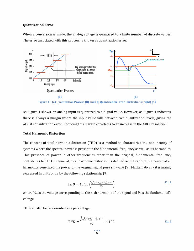
Quantization Error
When a conversion is made, the analog voltage is quantized to a finite number of discrete values.
The error associated with this process is known as quantization error.
(a)
(b)
Figure 4 – (a) Quantization Process (8) and (b) Quantization Error Illustrations (right) (4)
As Figure 4 shows, an analog input is quantized to a digital value. However, as Figure 4 indicates,
there is always a margin where the input value falls between two quantization levels, giving the
ADC its quantization error. Reducing this margin correlates to an increase in the ADCs resolution.
Total Harmonic Distortion
The concept of total harmonic distortion (THD) is a method to characterize the nonlinearity of
systems where the spectral power is present in the fundamental frequency as well as its harmonics.
This presence of power in other frequencies other than the original, fundamental frequency
contributes to THD. In general, total harmonic distortion is defined as the ratio of the power of all
harmonics generated the power of the original signal pure sin wave (5). Mathematically it is mainly
expressed in units of dB by the following relationship (9),
𝑇𝐻𝐷 = 10𝑙𝑜𝑔 𝑉2
2 + 𝑉32 + 𝑉4
2 + ⋯
𝑉𝑓2
Eq. 4
where Vhn is the voltage corresponding to the n-th harmonic of the signal and Vf is the fundamental’s
voltage.
THD can also be represented as a percentage,
𝑇𝐻𝐷 = 𝑉2
2 + 𝑉32 + 𝑉4
2 + ⋯
𝑉𝑓 × 100 Eq. 5

16
Total harmonic distortion is especially important in ADCs when building the input and sampling
blocks, as this report will further detail in its design section.
3.3 OVERSAMPLING CONVERTERS As mentioned in Section 3.1, one of the major types of converters is the oversampling ADC, which
exists in many variations. Oversampling ADCs are characterized as such due to having their
sampling frequency being much greater than twice the bandwidth of the signal, i.e. 𝑓𝑛 > 2 ∙
𝐵𝑎𝑛𝑑𝑤𝑖𝑑𝑡𝑠𝑖𝑔𝑛𝑎𝑙 . These types of circuits are implemented when attempting to obtain very high
accuracy. This precision is possible because the complex and precise analog circuitry is substituted
by the oversampling ADC’s use of digital signal processing techniques. The sacrifice that is made in
this case is the throughput that can be achieved (3).
Figure 5 - Block Diagrams for Nyquist and Oversampled ADCs
One of the advantages of oversampled ADCs is that aliasing is much less of a concern, in comparison
with Nyquist ADCs (3). That is because the signal’s frequency spectrum has frequencies much more
widely spaced, since the sampling rate is much greater than the signal’s bandwidth. A disadvantage
of oversampling converters is that a large amount of samples are require to perform a conversion
to a desired accuracy, versus the Nyquist ADCs, in which every conversion yields an individual
result.
Oversampled ADCs are a good option for converters where the signal is band limited, like music
systems, etc. Since this project is not an oversampling converter, these types of ADC’s will not be
explored further.

17
3.4 NYQUIST CONVERTERS A Nyquist ADC is a type of ADC that can resolve signals with frequencies up to ½ the sampling
frequency of the converter. This is the sampling rate adequate for recovering the original signal
according to the Nyquist theorem, i.e. 𝑓𝑛 = 2 ∙ 𝐵𝑎𝑛𝑑𝑤𝑖𝑑𝑡𝐴𝐷𝐶 , where fn is the sampling frequency
of the converter. There are several types of Nyquist ADCs in the analog design world. Johns and
Martin (9) compares the present ADC types with their common uses in terms of speed and
accuracy, shown below:
Table 2 - Speed and Accuracy Correlation with ADCs
Low-to-Medium Speed,
High Accuracy
Medium Speed,
Medium Accuracy
High Speed,
Low-to-Medium Accuracy
Integrating Successive Approximation
Flash
Two-Step
Interpolating
Oversampling Cyclic
Folding
Pipelined
Time-Interleaved
In the background portion of this paper, three types of converters that have been recently used in
the NECAMSID Lab will be explored: Pipelined, Successive Approximation, and Cyclic.
3.4.1 PIPELINED ADCS A common ADC structure, the pipeline converter receives its name from its multistage nature.
Figure 6 - Block Diagram of a 16-bit Pipelined ADC (8)

18
As Figure 8 shows, the analog input voltage VIN is sampled and enters the ADC. Each stage of the
converter is responsible for the quantization of a range of bits. Once a stage is completed, its output
residue voltage of becomes the next block’s input. A final block, containing an n-bit ADC resolves
the less significant bits of the converter. Finally a digital block receives each block’s output and
corrects for time and errors. The final decision is then composed.
3.4.2 SUCCESSIVE APPROXIMATION ADCS Successive-approximation ADCs are one of the most popular techniques for analog-to-digital
conversion since they are fairly quick in terms of conversion time, while having moderate circuit
complexity. There are several configurations that would qualify as successive-approximation
converters. For brevity of this report, the successive-approximation converter concept and a few
variations will be discussed in detail. For more complete descriptions of different types of
successive-approximation ADCs refer to (9).
Some authors recommend that the reader compare the functionality of a basic successive-
approximation converter as a “binary search” algorithm (9). An interesting way to think about this
algorithm is to imagine a book with 256 pages, in which you have to guess the page number
containing a specific event in the novel. However, you are only allowed to ask “yes/no” questions.
Therefore, using the binary search algorithm, one would try to approximate the number by first
asking the owner of the book if the event occurs on a page number greater than 128. If the answer
is no, then the next question would then address if the event occurs on a page number greater than
64. If so, then the remaining page range would then be divided by two and the same process would
be repeated. A flow chart presented by (10) is shown below:

19
Figure 7 - Flow Chart of Successive-Approximation Approach
The successive-approximation approach is similar to the anecdote above. The ADC works by
successively determining the bits of the output starting from the most significant bit (MSB) and
then checking the next bits. However, this method is very primitive for the world class types of
ADCs found today. Therefore, many improvements to that concept have been added, such as a
digital-to-analog converter (DAC) based approximation, using a block known as the Successive-
Approximation Register (SAR). A simple diagram of this functionality is shown below:
Figure 8 - DAC-based Successive-Approximation Converter (9)
In this case, a sample-and-hold block is usually needed so that the value being converted remains
constant through the conversion. The SAR is entirely digital and the DAC’s specifications will mostly
determine the speed and accuracy of the converter.

20
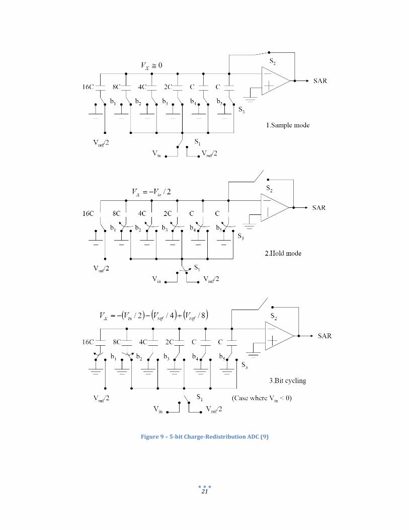
3.4.2.1 Charge Redistribution ADC
Shown in Figure 9 is an example of a charge-redistribution ADC (9). In this case, an array of
capacitors is used. Its advantage is that the sample and hold, DAC, and comparator blocks are all
combined into one block. The following chart explains the operation of Figure 9:
Table 3 - Charge-Redistribution (Figure 9) ADC Explanation
Operation
Mode Description
Sample All but the largest capacitor are charged to input voltage Vin while
comparator is being reset. The largest capacitor is set to Vref/2
Hold Comparator is taken off reset mode. Capacitors are switched to ground, with the exception of largest capacitor,
causing voltage on negative terminal of comparator Vx to become –Vin/2.
Bit Cycling If Vin is negative, the largest capacitor is switched to ground. If Vin is positive, the largest capacitor is remains at Vref/2.
Johns and Martin (9) catalogue other more complex types of SAR ADCs, which include calibration
and error correction blocks.
21
Figure 9 – 5-bit Charge-Redistribution ADC (9)

22
3.4.3 THE CYCLIC ADC A Cyclic converter, also known as an Algorithmic converter, is similar in operation to the successive
approximation converter. However, in the case of the Cyclic ADC, the reference voltage is not
altered. Instead, the error (or residue) of the amplifier is doubled (9).
Figure 10 – High Level Block Diagram of a Cyclic Converter (11)
As the block diagram above outlines, the operation of the cyclic converter functions in the following
manner: First, the input voltage is sampled by the sample-and-hold block. That value is then
compared to a threshold voltage, upon which a digital decision is made, determining a bit value in
the final sequence of the number sampled. A reference voltage is generated by a 1-bit digital-to-
analog converter which is dictated by the digital decision previously made. At the same time, the
input value is amplified by a factor two (ideally). The amplified value is then summed to a reference
voltage +/- VREF, leaving a residue voltage. The residue voltage then becomes the input of the
residue amplifier. This cycle is repeated enough times required to achieve the desired resolution,
earning the device its name. The sequence of decisions corresponds to the output value of the ADC.
3.4.3.1 Understanding the Residue Amplifier
A major part of the cyclic ADC is the residue amplifier. Therefore, in order to better comprehend the
operation of the ADC, a mathematical approach can be taken to explain this concept (11). The
equation below shows the relationship between the residue amplifier’s input and output:
𝑣𝑟𝑒𝑠𝑜𝑢𝑡= 𝐺 ∙ 𝑣𝑟𝑒𝑠 𝑖𝑛
− 𝑑 ∙ 𝑉𝑟𝑒𝑓 Eq. 6
where G is the gain of the amplifier and d is the digital decision.

23
Assuming ideal conditions, after performing N cycles, the amplifier exhibits the following negative
feedback loop relationship:
𝑣𝑟𝑒𝑠𝑜𝑢𝑡 (𝑁) = 𝐺𝑁 ∙ 𝑣𝑟𝑒𝑠 𝑖𝑛 − 𝐺𝑁−1𝑑1 + 𝐺𝑁−2𝑑2 + ⋯ + 𝐺0𝑑𝑁 ∙ 𝑉𝑟𝑒𝑓 Eq. 7
The output code of the ADC can be predicted by rearranging Eq. 7 into the following form (11):
𝑣𝑟𝑒𝑠 𝑖𝑛
𝑉𝑟𝑒𝑓=
1
𝐺𝑑1 +
1
𝐺𝑁−1𝑑2 + ⋯ +
1
𝐺𝑁𝑑𝑁 −
1
𝐺𝑁 𝑣𝑟𝑒𝑠𝑜𝑢𝑡 (𝑁)
𝑉𝑟𝑒𝑓
Eq. 8
The 1
𝐺𝑁 𝑣𝑟𝑒𝑠 𝑜𝑢𝑡 (𝑁)
𝑉𝑟𝑒𝑓 term of the equation can be redefined as the quantization error, and the first
term as the output code x:
𝑥 = 1
𝐺 𝑑1 +
1
𝐺
2
𝑑2 + ⋯ + 1
𝐺 𝑁
𝑑𝑁 Eq. 9
A plot relating the residue amplifier’s input and output can be created, as shown below:
Figure 11 - Residue Plot at G=2 (11)
Figure 12 - Residue Plot with G < 2 (11)
However, maintaining a constant gain of 2 may be challenging. Therefore, when G < 2, the residue
plot would look like Figure 12. This event makes it possible for two possible decisions for the same
input value, adding redundancy to the ADC. However, at the same time, it adds a level of complexity
to the calibration of the converter, which will be discussed in a further section of the document.

24
3.5 THE ROLE OF CAPACITORS As the previous section has outlined, the used of capacitors for ADCs is very common. As the design
sections of this paper will indicate, this ADC relies heavily on the use of multiple capacitors that will
be switched constantly to perform the cyclic function of the ADC. Therefore an understanding of
how the capacitors will affect this circuit and what constraints there are when choosing the correct
capacitors for our circuit is crucial.
3.5.1 THERMAL NOISE Thermal noise is inherent to all electronic circuits and it is caused by a random motion of electrons
in a conductor. It is a function of temperature and is constant over all frequencies. When designing
an analog to digital converter, this noise must be accounted for in the design of the sampling
capacitors in the sample-and-hold amplifier (SHA) in order to achieve a desirable signal-to-noise
ratio. Since the SNR is the integral of all the noise in a system, the lower the noise bandwidth, the
less noise is sampled by the ADC. Figure 13 below shows a model of a sample and hold switch with
a dc input and a thermal noise.
Figure 13- Diagram of Hold capacitor with Thermal Noise
When the sample switch is opened, the voltage on the capacitor is the DC signal plus the thermal
noise at the instant the switch is opened. Since the characteristic of the sample and hold circuit is a
low pass filter, the noise above the corner frequency of this low pass filter is attenuated. In order to
reduce the bandwidth of the noise the hold capacitor must be sized according to the SNR needed.
The equation below shows the relationship of capacitance and temperature to the RMS noise of a
system, which is the ratio of capacitor size to the total thermal noise power of the RC circuit.
𝑅𝑀𝑆 𝑛𝑜𝑖𝑠𝑒 = 𝐾𝑇
𝐶
Eq. 10

25
3.6 OPTIONS FOR OUTPUT DRIVING Every analog-to-digital converter has to interact with an off-chip digital domain, usually an FPGA or
a computer. Although sometimes designers may choose additional output drivers in their circuit at
the expense of simplicity, there are methods used to improve output performance. In this case,
various methods were researched. One particular method, known as Low Voltage Differential
Signaling (LVDS), showed itself to be a promising option for the circuit. Section 3.6 outlines the
existing configurations and applications of LVDS.
3.6.1 UNDERSTANDING LVDS Usually used for output blocks of ADCs, Low-Voltage Differential Signaling is a technology that was
officially introduced in 1994 by National Semiconductor. It was born out of the necessity to create
high performance solutions that consume little power and are susceptible to less noise than the
common techniques of the time, while being cost-effective, such as RS-442 and RS-485 standards. A
competing technology was Emitter Coupled Logic (ECL). However, it is incompatible with standard
logic levels, uses negative power rails, and leads to high chip-power dissipation (12).
Table 4 - Comparison Table of Differential Standards
3.6.2 THE CONCEPTS BEHIND LVDS LVDS, as the name suggests, is differential – meaning that it makes use of two signals to function. At
the cost of using an extra trace, space, and power, noise is considerably reduced through common-
mode rejection. As a consequence, many improvements can be made to the design, such as:
Signal swing can be dropped to only a few hundred millivolts due to signal-to-noise
rejection improvement
Rise time is shorter, resulting in faster data rates
Very low power consumption across a wide range of frequencies due to low swing and
current-mode driver outputs
Digital crosstalk onto analog circuitry is reduced

26
3.6.3 DIFFERENT TYPES OF LVDS The table below shows the different variations of LVDS found in the market today:
Table 5 - Industry Standards for Various LVDS Technologies (13)
While the concept of LVDS is the foundation of the standards found in the table above, there are
various applications for each one. Power consumption, performance, and target application are
among the differences listed above. For brevity, we will analyze the typical LVDS standard and how
it applies to this project. If applicable, the other technologies may be explored.
Different Configurations of LVDS
There are three common Bus types of LVDS configurations. They are:
Point-to-Point
Multidrop
Multipoint
3.6.3.1 Point-to-Point
Being the simplest configuration, Point-to-Point offers a direct path from the transmitter to the
receiver. This is favorable for use in the highest data rates, due to the simple path. A variation of
this configuration can be seen in Figure 15. All figures in this section are extracted from (12).
Figure 14 - Point-to-Point Configuration
Figure 15 - Data Distribution Using Point-to-Point Configuration

27
3.6.3.2 Multidrop
Multidrop is most efficient when various parts of a circuit need to receive the same information.
There is one driver and two or more receivers along the bus, as the figure below illustrates:
Figure 16 - Multidrop Configuration
3.6.3.3 Multipoint
A multipoint configuration uses various drivers and receivers. The advantage to this circuit is that it
can send information from multiple areas of the circuit, if necessary. However, this configuration
can get quite complex and speeds are generally lower than the other simpler configurations.
Figure 17 - Example of a Three-Node Multipoint Configuration
3.6.4 CONTRASTING LVDS TYPES AND CONFIGURATIONS The article released by National Semiconductor entitled “The Many Flavors of LVDS” (12)
summarizes the available technologies with the configurations used by them. This matrix is shown
below:
Table 6 - Bus Configurations vs. Standards

28
3.6.5 A TYPICAL LVDS CIRCUIT The following picture illustrates a high-level configuration for a LVDS circuit. Notice the detail
showing the reduction in interference due to the interaction in electric fields between the wires,
which are usually placed as a twisted pair.
Figure 18 - LVDS Driver and Receiver (13)
In the driver-receiver configuration shown in Figure 18, a 3.5mA current source is found in the
driver. Due to the high impedance “op-amp characteristic” of the receiver, all of the current flows
through the 350mV resistor in place. When the driver makes a switch, the current changes
direction of flow across the resistor and results in a logic state “one” or “zero.” Figure 19 illustrates
this concept.
Figure 19 - Digital Signaling Model

29
3.6.6 APPLICATIONS There are various applications for LVDS. As previously mentioned, the advantages presented by
LVDS make it a popular technology. Listed below are three common applications of LVDS within
integrated circuits.
Line drivers/receivers – Commonly used to convert single-ended signals into formats for
transmission over a cable or backplane.
SerDes – Serializer/deserializer pairs are used to multiplex a number of low-speed CMOS
lines and to transmit them as a single channel running at a higher data rate.
Switches – Used instead of bus architectures for high data rates. Commonly used for clock
distribution. LVDS is one of the most suitable signaling standards for clocks of any
frequency because of reliable signal integrity.
3.6.7 ASSESSING LVDS IN THE ADC DESIGN PROCESS There are various factors to consider when choosing a signaling standard, such as:
Required bandwidth
Ability to drive cables, backplanes, or long traces
Power budget
Network topology (point-to-point, multidrop, multipoint)
Serialized or parallel data transport
Clock or data distribution
Compliance to industry standards
Need or availability of signal conditioning

30
3.7 THE SPLIT-ADC CONCEPT One of the key characteristics in this project is the Split-ADC architecture. The figure below
illustrates the basic principle of the split-ADC. Instead of using one converter, the chip will have two
ADCs performing the same steps over the same input. The output then becomes the average of both
results. The difference of each ADC’s output is then sent to the error estimation block, which is
located off chip, in the digital realm (14).
Figure 20 - Illustration of Split-ADC Concept (11)
Ideally, the concept behind the split-ADC architecture is simple to comprehend: when the difference
between outputs xA and xB is zero, the calibration has occurred. This concept is important because it
will reduce the circuit’s calibration time significantly, as explained in (11). The following graph
contrasts the single ADC approach versus a split architecture.

31
Figure 21 - Split ADC Characteristics in Contrast with Single ADC Approach
As Figure 21 shows, the trade off in complexity is small compared to the advantages in calibration.
At the same time, the general speed, power and noise of circuit remains the same. This is because
the same parts are used but in proportions of one half the original size.
3.8 THE CURRENT MIRROR Biasing is very important to this project, making the necessity to build current sources imminent.
One of the most common forms of creating a current source is by using a MOSFET current mirror.
The current mirror relies on the assumption that transistors are closely matched, meaning that they
are fabricated under the same conditions, matching closely the values of the transistors’ threshold
voltages, mobility, and oxide capacitance. Therefore, since this level of matching and precision can
only be achieved in integrated circuits, the current is not commonly realized with discrete
components. Figure 22 shows a basic configuration for a current mirror.

32
Figure 22 - Current Mirror Example
According to the MOSFET Square Law, the current in the transistors can be defined as (3):
𝐼𝐷 =𝜇𝑛𝐶𝑜𝑥
2
𝑊
𝐿(𝑉𝐺𝑆 − 𝑉𝑡)2 Eq. 11
where ID is the MOSFET drain current, Cox is the capacitance of the oxide, W is the width of the
transistor, L is the length, VGS is the gate to source voltage and Vth is the threshold voltage of the
transistor. Therefore for the current ID1 in transistor M1, VGS1, can be solved.
𝑉𝐺𝑆1 = 2∙𝐼𝐷1 ∙𝐿1
𝜇𝑛𝐶𝑜𝑥 𝑊1+ 𝑉𝑡1 Eq. 12
As shown in Figure 22, by tying the MOSFET gates together, the following relationship is attained:
𝑉𝐺𝑆1 = 𝑉𝐺𝑆2
Using the value for VGS1 into the current of the second transistor:
𝐼𝐷2 =𝜇𝑛2𝐶𝑜𝑥 2
2
𝑊2
𝐿2
2∙𝐼𝐷1 ∙𝐿1
𝜇𝑛𝐶𝑜𝑥 𝑊1+ 𝑉𝑡1 − 𝑉𝑡2
2
Assuming the transistors are properly matched, the following assumptions can be made:
𝜇𝑛1 = 𝜇𝑛2
𝐶𝑜𝑥1 = 𝐶𝑜𝑥2
𝑉𝑡1 = 𝑉𝑡2

33
Simplifying the results to
𝐼𝐷2 = 𝐼𝐷1 𝑊2𝐿2
𝑊1𝐿1
Eq. 13
When comparing the current mirror to an ideal current source, the model falls short in a few
aspects. For example, an ideal source has infinite AC impedance, while a MOS mirror has finite
impedance. Also, the current mirror will have frequency limitations due to capacitive and inductive
parasitics.
3.9 THE DIFFERENTIAL PAIR The differential pair, sometimes referred to as the differential amplifier, is a vital part of this circuit.
According to Sedra and Smith, “the differential pair is the most widely used building block in analog
integrated-circuit design.” This is because differential amplifiers are less susceptible to noise than
their single-ended counterparts and they also allow for biasing of an amplifier without the use of
bypass and/or coupling capacitors, saving space on the chip being manufactured (15). As with the
current mirror, in integrated circuits, the differential pair relies largely on the ability to match
components.
The differential pair can be used in various configurations. In this section two modes of operation
will be explored: common-mode and differential gain modes. An example of a differential pair is
shown below:
Figure 23 - Differential Amplifier Example (16)

34
The differential pair consists of a symmetrical system of two MOSFETS sharing the same bias
current. The parameters in each transistor can be extracted using the square law equation, seen in
Eq. 11:
𝐼𝐷 =𝜇𝑛𝐶𝑜𝑥
2
𝑊
𝐿(𝑉𝐺𝑆 − 𝑉𝑡)2
where the currents at each transistor are equal to 𝐼𝐷
2.
3.9.1 BARTLETT’S BISECTION THEOREM The functionality of the system can be explored using Bartlett’s Bisection Theorem, which is based
on the symmetry of circuits and explores the fact that any two inputs can be represented in a
common mode and a differential mode.
Figure 24 –Amplifier Model
Figure 25 - Common Mode Model
Figure 26 - Differential Mode Model

35
The common-mode voltage can be defined as:
𝑉𝑐 =𝑉1+𝑉2
2 Eq. 14
And the differential voltage as:
𝑉𝑑 = 𝑉2 − 𝑉1 Eq. 15
Using this concept, it can be verified that:
𝑉1 = 𝑉𝑐 −𝑉𝑑
2 Eq. 16
and
𝑉2 = 𝑉𝑐 +𝑉𝑑
2 Eq. 17
The half circuit of each circuit model for the example in Figure 23 can be represented using the
bisection theorem, as shown below:
Figure 27 - Half-Circuit Model of the Common Mode
Figure 28 - Half-Circuit Model of the Differential Mode

36
A graph of the large signal characteristics of the differential pair is shown below:
Figure 29 - Signal Input-Output Characteristics of the Differential Input to Each Output
Figure 30 - Large Signal Input-Output Characteristic for the Differential Input to the Differential Output
To simplify calculations and circuitry it is common practice to attempt to operate with the linear
areas of the curves shown above. As was said in the introduction, the ingenuity of this project is that
the non-linearity is not as much of a pertinent issue in this circuit as will be explored in later
sections of this document.

37
4 HIGH-LEVEL DESIGN
The objective of this section is to give a brief high level overview of the integrated circuit being
designed for this project.
4.1 BLOCK DIAGRAM The figure below displays a proposed block diagram for the device. Several sub blocks are displayed
in the diagram. This approach gives us a modular idea of the design.
They main blocks found in this design are:
Switch Capacitor Array
Open Loop Differential Amplifier
Bias Circuitry
Comparator Network
Logic Sub Block
Output Drivers
Figure 31 - Block Diagram

38
The next sections of the report will dissect each of the blocks mentioned above and will outline how
each portion has been implemented.
5 THE INPUT BLOCK
The input of this ADC is composed of a sample-and-hold circuit which is used to obtain the input
signal onto the capacitors. This input block can appear quite complex because of the use of multiple
capacitors. Therefore, for simplicity a basic concept for the input block is shown below:
Figure 32 - Schematic of Input Block
As the figure above shows, in this simplified version of the input block, the input voltage Vin is
sampled onto capacitor C1. It is done so through a CMOS transmission gate, a configuration
involving a pair of opposite type MOSFETs. The use of transmission gates eliminates the
undesirable threshold voltage effects which give rise to loss of logic levels (3). The capacitor is
sampled at every positive of edge of the clock cycle, indicated in this case as Vclkp, and at every
negative edge of its inverted version, Vclkm, to bias the p-channel transistor.1
1 Note: Biasing for transistor M3 is simplified. In actual implementation, the gate voltage on M3 in Figure 32 is
delayed slightly to reduce charge injection.
39
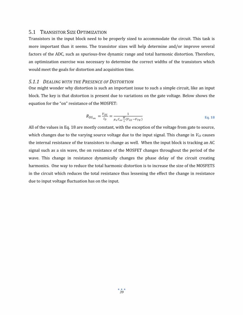
5.1 TRANSISTOR SIZE OPTIMIZATION Transistors in the input block need to be properly sized to accommodate the circuit. This task is
more important than it seems. The transistor sizes will help determine and/or improve several
factors of the ADC, such as spurious-free dynamic range and total harmonic distortion. Therefore,
an optimization exercise was necessary to determine the correct widths of the transistors which
would meet the goals for distortion and acquisition time.
5.1.1 DEALING WITH THE PRESENCE OF DISTORTION One might wonder why distortion is such an important issue to such a simple circuit, like an input
block. The key is that distortion is present due to variations on the gate voltage. Below shows the
equation for the “on” resistance of the MOSFET:
𝑅𝐷𝑆𝑜𝑛=
𝑉𝐷𝑆
𝐼𝐷=
1
𝜇𝑛𝐶𝑜𝑥𝑊
𝐿 𝑉𝐺𝑆 −𝑉𝑇𝐻
Eq. 18
All of the values in Eq. 18 are mostly constant, with the exception of the voltage from gate to source,
which changes due to the varying source voltage due to the input signal. This change in VGS causes
the internal resistance of the transistors to change as well. When the input block is tracking an AC
signal such as a sin wave, the on resistance of the MOSFET changes throughout the period of the
wave. This change in resistance dynamically changes the phase delay of the circuit creating
harmonics. One way to reduce the total harmonic distortion is to increase the size of the MOSFETS
in the circuit which reduces the total resistance thus lessening the effect the change in resistance
due to input voltage fluctuation has on the input.

40
5.1.2 PERFORMING A PARAMETRIC ANALYSIS The goal for this analysis was to determine the appropriate input block’s transistor widths. From
previous design experience, professor McNeill recommended the following assumptions:
The p-channel (M2) transistor will have a width that is 4 times larger than its n-channel
MOSFET equivalent
The n-channel MOSFET (M3) on the top plate of the capacitors should have a width
proportional (by a factor of x), but not necessarily equal, to the n-channel MOSFETs (M1) on
the bottom plate
This optimization can be thought of as the total area used by the entire input block. Therefore, the
total area can be found by determining the total width, WTotal, as a function of M1’s width, as shown
below:
𝑊𝑇𝑜𝑡𝑎𝑙 = 𝑊𝑄1+ 𝑊𝑄2
+ 𝑊𝑄3= 𝑊 + 4𝑊 + 𝑥𝑊 Eq. 19
Rearranging, 𝑊𝑇𝑜𝑡𝑎𝑙 = 5 + 𝑥 ∙ 𝑊
𝑊 =𝑊𝑇𝑜𝑡𝑎𝑙
5+𝑥 Eq. 20
As a result, a series of graphs were created where the values for x, W, and WTotal were swept, to find
the smallest transistors that would fit the parameters. The two main characteristics that relate to
these values are acquisition time and total harmonic distortion. To deliver values for those
attributes, several parametric analyses have been completed in ICFB. The following table indicates
the values that were simulated:
Table 7 - Swept Attributes
x 0.1 0.2 0.5 1 2 5 10
WTotal 10µm 20µm 50µm 100µm 200µm 500µm 1mm 2mm 5mm 10mm
The title of each graph indicates the values used for WTotal. On the y-axis, the red lines indicate THD
and the blue lines indicate acquisition time. The x-axis indicates the value of x.
Note: The values of x are scaled by a factor of 20, in order to accommodate simulation criteria in Cadence.

41

42

43
The results are summarized in the table below:
Table 8 - Summarized Optimization Results of tACQ and THD
WTotal
[µm] x tACQ
[ns] THD [%]
10 0.25 85 1.8 20 0.5 50 1.0 50 0.5 30 0.6
100 0.5 12 0.3 200 0.5 6 0.15 500 0.5 3 0.06
1000 0.5 1.9 0.035 2000 0.5 1.5 0.025 5000 0.5 1.1 0.016
10000 0.5 1.09 0.012
The values chosen were dictated by minimum of THD, which happened at the lower side of
acquisition time curve. It can be observed that there is a relationship between the total width of the
transistors and the parameters simulated. This relationship is shown below in Figure 33 and Figure
34.
Figure 33 - THD and WTotal Relationship
Figure 34 - Acquisition Time and WTotal Relationship
As the figures above indicate, the larger widths will give us better performance. However, the die
area must also be accounted for because of the rather large percentage of the final IC the input
block uses. This meaning that a compromise will be made. As a result, the next step was to set goals
for distortion and acquisition time that will establish the basis for this compromise.

44
5.1.2.1 Goals for Parameters
To ensure that the design is competitive, Professor McNeill has indicated that from experience, the
level of total harmonic distortion should be less than 0.01%. Once again, the Professor’s experience
in analog integrated circuit design served as a guide for a harmonic distortion goal. As defined in
the introduction of the paper, the ADC will perform one million samples per second, translating into
1 conversion per microsecond. Therefore, twenty percent of this time has been allocated for
sampling the input for reasons which will be discussed later. Because of this, the goals for this ADC
input parameters are as follows:
Table 9 - Parameter Goals
Parameter Goal
Total Harmonic Distortion < 0.01%
Acquisition Time < 200 ns
As the graphs show, thqe acquisition time is not an issue for us, since all measurements met the
required goal. The reason for such a loose acquisition time goal will be explained in a further
subsection.
5.1.3 CHOOSING TOTAL WIDTH When looking at the simulation results, the total harmonic distortion levels found were not below
the expected mark of 0.01%. The reason for this is inferred to be the limitations of the simulator.
The simulations were done under various conditions and yielded different results. However, when
looking at Cadence’s description of the THD formula, some parameters were not easily editable. As
a result, an assumption was made that the total harmonic distortion levels are low enough at a very
safe margin at a WTotal value of 5mm.
As stated in Eq. 20, the equation derived gives the parameters for width is:
𝑊 =𝑊𝑇𝑜𝑡𝑎𝑙
5+𝑥
Since it has been established that the total width for the input block is 5mm, the total with W from
Table 9 is 909um as seen below.
𝑊 =5𝑚𝑚
5+0.5
𝑊 = 909µ𝑚
45
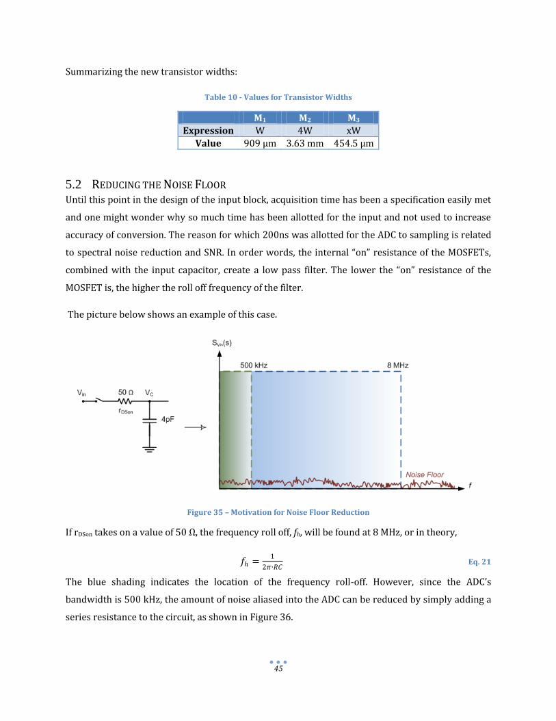
Summarizing the new transistor widths:
Table 10 - Values for Transistor Widths
M1 M2 M3
Expression W 4W xW
Value 909 µm 3.63 mm 454.5 µm
5.2 REDUCING THE NOISE FLOOR Until this point in the design of the input block, acquisition time has been a specification easily met
and one might wonder why so much time has been allotted for the input and not used to increase
accuracy of conversion. The reason for which 200ns was allotted for the ADC to sampling is related
to spectral noise reduction and SNR. In order words, the internal “on” resistance of the MOSFETs,
combined with the input capacitor, create a low pass filter. The lower the “on” resistance of the
MOSFET is, the higher the roll off frequency of the filter.
The picture below shows an example of this case.
Figure 35 – Motivation for Noise Floor Reduction
If rDSon takes on a value of 50 Ω, the frequency roll off, fh, will be found at 8 MHz, or in theory,
𝑓 =1
2𝜋∙𝑅𝐶 Eq. 21
The blue shading indicates the location of the frequency roll-off. However, since the ADC’s
bandwidth is 500 kHz, the amount of noise aliased into the ADC can be reduced by simply adding a
series resistance to the circuit, as shown in Figure 36.

46
Figure 36 - New Input Circuit Model with Added Resistor
To find the correct value for this resistance, the acquisition time must be taken into account to
obtain the precision desired for the ADC. Since this converter should be 16-bit linear, the input
accuracy must be within ½ a Least Significant Bit of the ADC, as shown below:
𝑡𝑎𝑙𝑙𝑜𝑤 = ln 217 ∙ 𝜏 Eq. 22
where τ is the RC circuit’s time constant and tallow is the value pre-determined as the input sampling
duration. Restructuring the equation, we’ll have:
𝜏 =𝑡𝑎𝑙𝑙𝑜𝑤
ln 217 ≈
200 𝑛𝑠
12= 16 𝑛𝑠
Knowing that 𝜏 = 𝑅𝐶 time constant is 16ns, the resistor size can be solved since the capacitor
value has been set to be 4pF on C1,
𝑅 =16 𝑛𝑠𝑒𝑐
4𝑝𝐹
𝑅 = 4𝑘𝛺
As expected, the input block will now have its acquisition time increased drastically. However, since
there is 200ns allotted for the sampling of the circuit there room for this increase. To ensure the
acquisition time is under 200ns, the figure below shows the acquisition time according to the
different resistance values from 0 to 10kΩ:

47
Figure 37 - Acquisition Time Dependence after Adding New Resistor
5.2.1 RESISTOR TOLERANCE According to the JAZZ library help files, the resistor tolerances will vary approximately by 25%.
That assumption is made based on the following documentation:
Therefore, once can see that this circuit may have a higher acquisition time than expected with a
5kΩ resistor. However, even with a 25 percent increase of resistance the acquisition time is still
below the 200ns mark.
Table 11 – Effect of Tolerances
-25% Expected +25%
Value 3 kΩ 4 kΩ 5 kΩ tACQ 111 nsec 148 nsec 185 nsec
To see the variation, the THD was also simulated. It can see that the swing in distortion does not
vary much when the resistor is varied, as shown in Figure 38.

48
Figure 38 - THD Dependence on Resistor Variation
Using Eq. 21, the roll-off frequency will now be
𝑓 =1
2𝜋∙𝑅𝐶=
1
2𝜋∙16𝑛𝑠= 9.95 𝑀𝐻𝑧
𝑓 ≈ 10 𝑀𝐻𝑧
As stated in Section 3.5.1, the SNR of ADC is the integral of all the noise in a system. Therefore, by
reducing total bandwidth of the input of the ADC the signal-to-noise ratio is reduced as well.
5.2.2 IMPLEMENTATION OF INPUT BLOCK In the actual input block designed for this ADC, a 4 capacitor implementation chosen with a
capacitor size of 1pF. Therefore all transistors need to be sized accordingly. The next page shows a
diagram of this concept.

49
Vclkp
Vclkm
C1A
Vicm
Vinp
Vdd
N-MOS
P-MOS
N-MOS
Vclkp
WL
0.25WL
xWL
C1B
C1C
C1D
Rin1
C2A
C2B
C2C
C2D
Vicm
Vclkp
Rin2
Vinm
N-MOS xWL
Vclkp
Vclkm
Vdd
N-MOS
P-MOSWL
0.25WL
Vclkp
Vclkm
Vdd
N-MOS
P-MOSWL
0.25WL
Vclkp
Vclkm
Vdd
N-MOS
P-MOSWL
0.25WL
Vclkp
Vclkm
Vdd
N-MOS
P-MOSWL
0.25WL
Vclkp
Vclkm
Vdd
N-MOS
P-MOSWL
0.25WL
Vclkp
Vclkm
Vdd
N-MOS
P-MOSWL
0.25WL
Vclkp
Vclkm
Vdd
N-MOS
P-MOSWL
0.25WL

50
5.2.3 LAYOUT OF THE INPUT BLOCK When creating the layout of this input block it was imperative to have a low resistance path to
charge and discharge the gates of the MOSFET’s. This is due to the extremely high gate capacitance
inherent in the large size of the MOSFET’s. The large gate capacitances create high surge currents
when switching and to increase the speed of switching large metal runs are needed between the
input buffers and the input MOSFET’s. Figure 39 below shows the layout of the input block of the
Cyclic Converter.
Figure 39 - Layout of Input Block

51
6 THE SWITCHED CAPACITOR NETWORK
One of the key characterisitcs of the Cyclic ADC is that it is able to use sampled values after a
decision has been made and apply those values to the residue amplifier. The ability to do analog
math with these values and sample the input with ease comes from the switch capacitor array.
Figure 40 - Switch Capacitor Array Block and its Interaction with other Blocks
The switch capacitor network interacts with every block of the design, since the values on the
capacitor dictate the input and output values of the ADC.
It is not surprising that an extensive amount of time was spent in this network. This section will
serve to explain the various switch capacitor designs create and the reasons why those designs
were discontinued.

52
6.1 DEFINING THE CORRECT NUMBER OF CAPACITORS FOR THE NETWORK A crucial part of the design of the Cyclic ADC is to decide how many capacitors will be used in the
DAC. More capacitors allow for more configurations but adds to the level of complexity by using
additional transistors for switching and transmission.
6.1.1 USING ONE CAPACITOR Using one capacitor as seen by the figure below means that there is one capacitor on each input and
one capacitor on each output of the differential amplifier. The differential counterpart is not
considered in this example for simplicity. One capacitor means that the amplifier’s input will have
one capacitor and the amplifier’s output will have one capacitor as well. This number is doubled for
the differential functionality.
Figure 41 - Example of Using One Capacitor
Although the approach of using one capacitor makes the circuit’s functionality very simple, this
approach proved to be ineffective immediately. This is due to a simple factor. Symbolized in the
graph as VDAC is the block responsible for choosing a decision based on a previous block. The
decision created by this block results in the switching to its respective voltage reference. However,
since the differential amplifier does not have a perfect gain of 2, two additional decisions need to be
made. With this design, two additional voltage references would need to be created. Since industry
standards and common practice usually limit the amount of off-chip reference voltages, it was
necessary to introduce an extra capacitor to incorporate decisions -2, -1, 0, +1, and +2.

53
6.1.2 USING TWO CAPACITORS To incorporate the desired decisions, the use of 2 capacitors was then implemented. Since there is a
positive, negative, and common mode reference voltage available for each capacitor, the resulting
decision would be represented as the diagram below indicates:
Figure 42 - Diagram of Decisions with 2 Capacitors
Figure 42 shows the position of the references in each of the 5 decisions. The voltages Vrefp Vrefm and
Vicm can be thought of “+2” , “-2” and “0” respectively due to the fact that Vicm is the zero reference
and Vrefp and Vrefm are ±0.34V away from Vicm it can be proven that these switching modes will
produce the equivalent reference of ±0.17V away from Vicm. Since each capacitor is ½ the size as in
the original one capacitor implementation the total capacitance does not change.
𝑃𝑙𝑢𝑠 1 = 𝑉𝑟𝑒𝑓𝑝 +𝑉𝑖𝑐𝑚
2
Eq. 23
𝑃𝑙𝑢𝑠 1 = 1.43𝑉+1.09𝑉
2= 1.26𝑉
𝑀𝑖𝑛𝑢𝑠 1 = 𝑉𝑟𝑒𝑓𝑚 +𝑉𝑖𝑐𝑚
2
Eq. 24
𝑀𝑖𝑛𝑢𝑠 1 = 0.77 𝑉+1.09𝑉
2= 0.93𝑉 Eq. 25
The voltages 1.26𝑉 and 0.93V correspond to the ±1 decision voltage levels.

54
6.1.3 TESTING THE TWO CAPACITOR SYSTEM As the testing indicated, implementing the ±1 decisions was now possible, but not as effective as
expected. The circuit used for testing this decision is shown below:
Figure 43 - Test Circuit for +/- 1 Decision
In other decisions, no charge is redistributed into the capacitors before switching. However, in this
case, the issue lies with the fact that in the ± 1 decision mode, there is a 0.34V difference on the top
plates of the capacitors. Since the top plates are connected to eachother, charge flows from one
capacitor into another implementing the avereging function. This DAC decision must be done in
less than a nanosecond in order to give the differential amplifier enough time to settle itself. In
order for this to be done the resistance of the switches connecting the bottom plates to Vicm , Vrefp
and Vrefm must be sufficently low. The main problem with this design was that the MOSFET switch
controlling Vicm had a very low overdrive voltage causing the transistor to stay in the saturation
region only allowing a small amount of current to flow. This caused the Nmos transistor connecting
Vicm to the bottom plate of the capacitor to be sized 20 times as large as the Vrefm transistor. This
caused a substantial amount of charge from the channel of the MOSFET to be forced into the 2pF
capacitor when the transistor was turned off, causing a large change in voltage in the capacitors
holding voltage information of the previous cycles. Figure 44 shows this charge injection affecting
the input.

55
Figure 44- Example of Charge Injection: Capacitor being Switched between a 500µm PMOS and a 250µm NMOS
As the transient response above shows, the charge forced into the capacitor changes the voltage
across the capacitor by over 100mV as indicated by point M1. Therefore a new alternative had to be
created that did not use Vicm to make critical DAC decisions.
6.2 THE FINAL SWITCH CAPACITOR DESIGN: FOUR CAPACITORS The approach in resolving this issue was to try to minimize avoid the use of Vicm for decisions that
needed charge redistribution. Instead four capacitors would be used to achieve the same result of
the 5 DAC decisions while avoiding Vicm. In this model each capacitor would have ¼ of the original
capacitance causing die area to not increase by a substantial amount. The four capacitor model
enabled the decisions to be made to make the decisions as seen in Figure 45.
Figure 45 - Method for Using 4 Capacitors

56
Using this design the ±1 decisions will be made without the use of Vicm as follows.
𝑃𝑙𝑢𝑠 1 = 3∗ 𝑉𝑟𝑒𝑓𝑝 +𝑉𝑟𝑒𝑓𝑚
4
Eq. 26
𝑃𝑙𝑢𝑠 1 = 3∗ 1.43𝑉+0.77𝑉
4 = 1.265V
𝑀𝑖𝑛𝑢𝑠 1 = 3∗ 𝑉𝑟𝑒𝑓𝑚 +𝑉𝑟𝑒𝑓𝑝
4
Eq. 27
𝑀𝑖𝑛𝑢𝑠 1 = 3∗0.77𝑉+1.43𝑉
4 = 0.935V
It can be seen that the 4 capacitor implementation yields a similar result as the 2 capacitor
approach as seen in the table below.
Table 12 - Comparison of Decisions
Decision 2 Capacitor
Implementation 4 Capacitor
Implementation
+2 1.43V 1.43V +1 1.26V 1.265V 0 1.09V 1.1V -1 0.93V 0.935V -2 0.77V 0.77V
Figure 46 shows a test circuit used to simulate the 4 capacitor approach:
Figure 46 - Circuit Implemented with 4 Capacitors

57
Using the 4 capacitor implementation, the overdrive voltages for the MOSFETS are much greater,
reducing the Rdson of the MOSFETs allowing much smaller transistor widths to be used. Using this
implementation, charge injection is reduced by a factor of about 21. Figure 47 and Figure 48 below
shows a comparison of the 2 capacitor model and the 4 capacitor model for the implementation of
the +1 decision.
Figure 47 - 2 Capacitor Implementation of “+1” Decision
Figure 48 – 4 Capacitor Implementation of “+1” Decision
As seen in the figures above, the charge injection is reduced from 108mV to 5mV a factor of more
than 21 improvements, while still complying with the 1ns charge redistribution time. Another
advantage of using the 4 capacitor design is that due to the enormous decrease in MOSFET width,

58
the overall die area for the design is actually reduced. Figure 49 shows a schematic representation
of the switched capacitor network including a model of the parasitic on the top and bottom plates of
the capacitors. Each of the 1pF capacitors has 250fF of parasitic capacitance on their bottom plates
and a combined 40fF capacitance on the node connecting the top plates of the capacitors.

Figure 49- Switched Capacitor Circuit
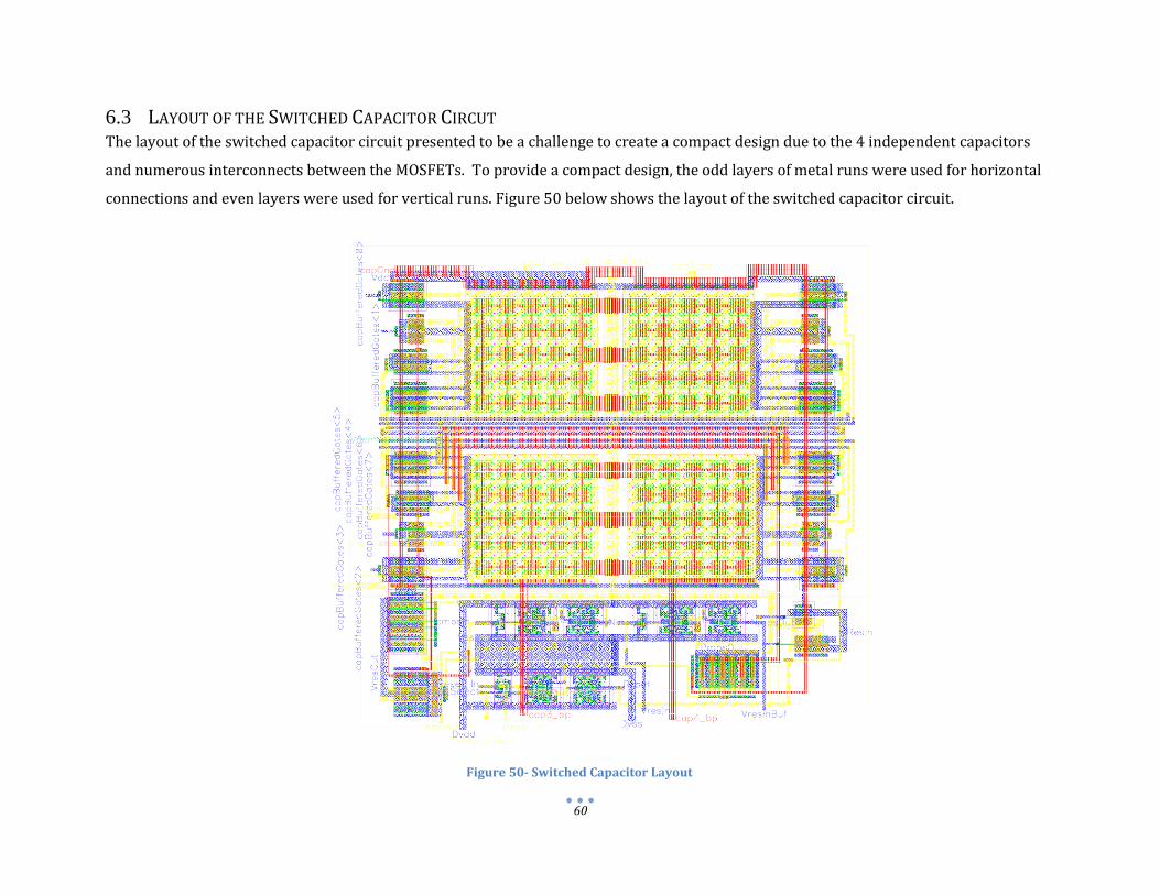
60
6.3 LAYOUT OF THE SWITCHED CAPACITOR CIRCUT The layout of the switched capacitor circuit presented to be a challenge to create a compact design due to the 4 independent capacitors
and numerous interconnects between the MOSFETs. To provide a compact design, the odd layers of metal runs were used for horizontal
connections and even layers were used for vertical runs. Figure 50 below shows the layout of the switched capacitor circuit.
Figure 50- Switched Capacitor Layout

61
6.4 DETERMINING VOLTAGE REFERENCE VALUES FOR SWITCHED CAPACITORS The voltage references being used by the ADC were originally found when using a two capacitor
approach. However, the reference voltages were kept for the four capacitor approach due to the
similarities in the design. The solution is based on the principle that the positive and negative
reference voltages can be found when the difference between them is the common output voltage
after shorting the inputs and outputs of the differential amplifier.
Figure 51 - Derivation for Reference Voltages
Therefore, the following two equations can be derived:
𝑉𝑟𝑒𝑓𝑚 − 𝑉𝑜𝑢𝑡𝑚𝑖𝑛 − 𝑉𝑜𝑐𝑚 = 𝑉𝑖𝑐𝑚 Eq. 28
𝑉𝑟𝑒𝑓𝑝 − 𝑉𝑜𝑢𝑡𝑚𝑎𝑥 − 𝑉𝑜𝑐𝑚 = 𝑉𝑖𝑐𝑚 Eq. 29
which, after some basic manipulation, will turn into:
𝑉𝑟𝑒𝑓𝑚 = 𝑉𝑖𝑐𝑚 + 𝑉𝑜𝑢𝑡𝑚𝑖𝑛 − 𝑉𝑜𝑐𝑚 Eq. 30
𝑉𝑟𝑒𝑓𝑝 = 𝑉𝑖𝑐𝑚 + 𝑉𝑜𝑢𝑡𝑚𝑎𝑥 − 𝑉𝑜𝑐𝑚 Eq. 31
Plugging in the values (specified in section 6.6):
𝑉𝑟𝑒𝑓𝑚 = 1.09𝑉 + 0.96𝑉 − 1.3𝑉
𝑽𝒓𝒆𝒇𝒎 = 𝟎. 𝟕𝟓𝑽
𝑉𝑟𝑒𝑓𝑝 = 1.09𝑉 + 1.64𝑉 − 1.3𝑉
𝑽𝒓𝒆𝒇𝒑 = 𝟏. 𝟒𝟑𝑽

62
DIFFERENTIAL AMPLIFIER
The differential amplifier block is the heart of the residue amplifier. Figure 52 shown below is the
schematic of the differential amplifier and its supportive circuitry. The behavior of the differential
amplifier and equations that governed its qualitative analysis was introduced previously in section
3.9. The role of each supportive component will be described in separate sections that follow. The
goal regarding the design of the differential amplifier was using an open-loop differential amplifier
in order to reduce the power consumption and complexity. The nonlinearity introduced by the
open-loop configuration is compensated for in the off chip calibration routine.
Figure 52-Schematic Representation of Differential Amplifier
6.5 FUNDAMENTAL COMPONENTS OF THE DIFFERENTIAL AMPLIFIER There are 4 main blocks in the design of the differential amplifier as seen below
The main part of this circuit is the differential pair
The Replica bias sub circuit
Resetting transistors to short inputs and outputs
A source follower used to set the gate voltage for the bias transistors

63
The topology used for the load of the differential amplifier is the resistive load. The reason for using
a resistive load is that the maximum gain needed for this application is a gain of two, which is a
small gain that easily can be achieved by the resistive load configuration. Therefore, the use of a
resistive load topology meets the constraint being faced (low gain) and minimizes the complexity of
the circuit.
6.6 DIFFERENTIAL AMPLIFIER VOLTAGE LEVELS Another aspect of the differential pair design was choosing the input, output, and common mode
voltage levels for the device. In order to start the design for this part known variables were listed
and several assumptions were initially considered.
Power supply rails range from ground (VSS = 0V) to VDD = 1.8V.
Threshold voltage for the transistors used in designing the differential amplifier was
selected, Vth = 0.45V. The threshold voltage was found in the available Jazz libraries.
Figure 53- Differential In-Out Characteristic
The derivation of the voltage levels started based on four equations, which will be discussed in this
section. The first set of equations involves determining the triode crashes within the differential
amplifier. The derivation of the following equations were based on the limitations that differential
amplifier faces. Below is shown the input output characteristic graph for the differential amplifier
which served as a guide to derive the equations that govern the input and output ranges of the
differential pair.
The low triode crash happens when inputs are equal to each other. In other words:

64
𝐿𝑜𝑤 𝑡𝑟𝑖𝑜𝑑𝑒 𝑐𝑟𝑎𝑠 → 𝑉𝐼𝑃 = 𝑉𝐼𝑀 = 𝑉𝐼𝐶𝑀 Eq. 32
An assumption made regarding the transistor, M9, that serves as the biasing of the differential
amplifier was that the minimum drain to source voltage must be equal to, VDS = 0.3V for this device
to be in saturation region.
Below are shown known voltages and the equation for the gate to source voltage for M1.
Vth = 0.45V
VDS = 0.3V
𝑉𝐺𝑆1 = 𝑉𝑡 + 𝑉𝑜𝑣1 Eq. 33
The four base equations used were the following;
Eq. 34 describes the low triode crash of the device:
𝑉𝐼𝐶𝑀 − 𝑉𝑡 + 𝑉𝑜𝑣1 = 0.3𝑉 Eq. 34
Equation Eq. 35 describes the high triode crash of the device:
𝑉𝑡 − 0.15 = 𝑉𝐼𝐶𝑀 +𝑉𝐼𝑅
2 − 𝑉𝑂𝐶𝑀 +
𝑉𝑂𝑅
2 Eq. 35
Equation Eq. 36 describes the output voltage range for the differential pair that is given by:
𝑉𝑂𝑅 = 𝐺 ∗ 𝑉𝐼𝑅 Eq. 36
Equation Eq. 37 relates the input range of the differential amplifier assumed to be at a value
approximately equal to M1 overdrive voltage:
𝑉𝐼𝑅 ≈ 𝑉𝑜𝑣1 = 0.15V Eq. 37
By using all the assumptions made above and values available, the VICM value can be found as shown.
Plugging in Vth and solving for VICM, the following is obtained:
𝑉𝐼𝐶𝑀 = 𝑉𝐼𝑅 + 0.75𝑉 Eq. 38
The next step is to solve Eq. 35. Using Eq. 36, VOR for 2VIR, can be substituted to get the following:

65
𝑉𝑡 − 0.15 = 𝑉𝐼𝐶𝑀 +𝑉𝐼𝑅
2 − 𝑉𝑂𝐶𝑀 −
2∗𝑉𝐼𝑅
2
0.45 − 0.15 = 𝑉𝐼𝐶𝑀 +𝑉𝐼𝑅
2 − 𝑉𝑂𝐶𝑀 − 𝑉𝐼𝑅
0.3 = 𝑉𝐼𝐶𝑀 +3𝑉𝐼𝑅
2− 𝑉𝑂𝐶𝑀 Eq. 39
The next step is to substitute VICM from Eq. 38:
0.3 = 0.75 + 𝑉𝐼𝑅 +3𝑉𝐼𝑅
2− 𝑉𝑂𝐶𝑀
Reordering the equation to solve for VOCM as a function VIR:
𝑉𝑂𝐶𝑀 =5𝑉𝐼𝑅 +0.9
2
Eq. 40
Respectively, VIR could be solved for:
𝑉𝐼𝑅 =2𝑉𝑂𝐶𝑀 −0.9
5 Eq. 41
Finally, VICM must be found. To do so, Eq. 41 will be inserted into Eq. 38, obtaining:
𝑉𝐼𝐶𝑀 = 2𝑉𝑂𝐶𝑀 −0.9
5+ 0.75
Eq. 42
With these results, a plot of the equations on the same axes is shown below since all equations are
represented as a function of VIR:
Figure 54 - Voltage Ranges Plot

66
The voltages shown on Figure 54 can be used to observe the impact of changing the voltage ranges
of the circuit. As the figure above shows, we can use the point of intersection between VICM and VIR
as the choice for voltage ranges:
𝑉𝑖𝑟 = 0.34𝑉
𝑉𝐼𝐶𝑀 = 1.09𝑉
𝑉𝑜𝑟 = 0.64𝑉
𝑉𝑂𝐶𝑀 = 1.3𝑉
Once the above voltage levels were found, they were used in the derivations of the resistive load
values and the differential pair bias current.
6.6.1 KT/C CAPACITOR SIZING The sampling capacitor size for the sample and hold circuit is determined by the KT/C noise floor
the input voltage range and the desired SNR. Eq. 48 below shows the relationship of capacitance
and temperature to the RMS noise of a system. In order to achieve a 12 bit noise floor for this ADC
an SNR of 74 db would be necessary.
𝑆𝑁𝑅 = 6.02db ∗ N + 1.76 db Eq. 43
𝑆𝑁𝑅 = 6.02db ∗ 12bits + 1.76 db = 74db
In order to achieve an SNR of 74 db a minimum capacitance value of 3.63pF would be needed
achieve a 74db resolution. The capacitors chosen in this circuit is 2pF as seen in Eq. 49 in order to
take into account differences from the ideal ADC quantization error and the split cyclic design.
𝐶 =1
2∗
2𝐾𝑇
𝑉𝑖𝑛 ∗
22
10
𝑆𝑁𝑅 20
2 Eq. 44
𝐶 =1
2 ∗
2∗1.3806∗10−23∗303.15𝐾
𝑉𝑖𝑛 ∗
22
10
74𝑑𝑏 20
2 = 1.81 𝑝𝐹
The scalar factor of ½ was introduced to accommodate the split architecture of this ADC, which has
two independent half ADC’s simultaneously converting the same input. Each of these half ADC’s
uses 2pF capacitors which increase the noise by a factor of 2 from a more traditional designed
single cyclic ADC with 4pF capacitors. This increase in noise from each half ADC would then be

67
averaged since both half ADC’ are converting the same input to a digital code, which would reduce
the noise by 2 thus having no net change KT/C noise from an overall system perspective.
6.6.2 DERIVATIONS OF RESISTIVE LOAD VALUES AND BIAS CURRENT Proper biasing of the differential amplifier is an essential part in this design. In the differential pair
circuit the bias current determines factors such as the slew rate of the amplifier, speed and
acquisition time of the amplifier while keeping all of the internal MOSFETs in their active region.
For the differential pair bias current there is a tradeoff of power consumption and speed. The faster
the settling time needed to achieve a small error margin, the more current is needed to bias the
differential pair. In this circuit, the voltage on the load capacitor needs to be resolved to 14 bits
accuracy in less than 20ns.
In order to acquire a signal and resolve to 14 bits resolution on the load capacitor there must be at
least 9.7τ (RC time constants) as shown in the equation below:
ln 2− # 𝑜𝑓 𝑏𝑖𝑡𝑠 𝑡𝑜 𝑟𝑒𝑠𝑜𝑙𝑣𝑒 = # 𝑜𝑓 τ 𝑛𝑒𝑒𝑑𝑒𝑑 𝑡𝑜 𝑎𝑐𝑖𝑣𝑒 𝑟𝑒𝑠𝑜𝑙𝑢𝑡𝑖𝑜𝑛 Eq. 45
ln 2−14 = 9.7τ Eq. 46
To find the resistance needed to achieve at least 9.7τ in the 20ns allotted we must find what τ is in
the circuit, which is seen in the equations below:
τ = 20𝑛𝑠
10= 2𝑛𝑠 Eq. 47
With the RC time constant known and the capacitance value assumed to a certain value as shown
below, the resistance necessary for the resistor load for the differential pair can be calculated by
making a use of the equation below:
𝑅 = τ
C Eq. 48
The capacitor value used in the above equation was chosen to be, C = 2pF. The C value was decided
while keeping in mind the SNR requirement in this project. For SNR description refer to section 3.2.
After putting all values in the resistor equation the resistor value needed for differential amplifier
load was found to be:
𝑅 =2.061𝑛𝑠
2𝑝𝐹= 1030.6Ω ≈ 1𝐾Ω Eq. 49

68
Knowing the values of the resistors in the resistive load portion of the ADC and the 𝑉𝑜𝑐𝑚 one can
calculate the bias current needed to operate the differential pair. The equation below is used to
determine the current through each branch of the differential amplifier:
𝐼𝐵𝑖𝑎𝑠
2=
𝑉𝑑𝑑−𝑉𝑜𝑐𝑚
𝑅𝑟𝑒𝑠𝑖𝑠𝑡𝑜𝑟 𝑙𝑜𝑎𝑑 Eq. 50
Plugging the values from above the current through one branch of the differential pair results to be:
𝐼𝐵𝑖𝑎𝑠
2=
1.8𝑉−1.3𝑉
1𝐾Ω= 500µ𝐴 Eq. 51
Therefore, the differential pair bias current would be the sum of the currents from both branches
that results to be:
𝐼𝐵𝑖𝑎𝑠 = 𝐼𝐵𝑖𝑎𝑠
2+
𝐼𝐵𝑖𝑎𝑠
2= 1𝑚𝐴 Eq. 52
6.7 REPLICA BIAS ANALYSIS A replica bias circuit is designed to mimic the behavior of the differential pair. That way, variations
from the input are accounted for by helping to stabilize VDS. One of the advantages of such circuitry
is that it applies a reference voltage to a targeted transistor in order to keep the current mirror as
consistent as possible with input voltage.
6.7.1 ADVANTAGES AND PURPOSE OF USING REPLICA BIAS The use of replica bias minimizes the channel length modulation on the current bias source. Replica
bias creates the same VDS as the original circuit being replicated, thus minimizing channel length
modulation. Designing a replica bias circuit requires a special care in terms of transistor matching.
As the name of this circuit suggests, it replicates the behavior and functions of the circuit that it
supports, in this case the differential amplifier. The transistors in the replica bias is a facto/r of 10
smaller compared to the transistors in the differential pair in order to minimize the current usage,
die area, and power consumption of the replica bias by a factor of 10.
6.7.2 DESIGNING REPLICA BIAS The role of the source follower in the circuit is that it sets the bias gate voltage by subtracting a
constant voltage, 309.5mV, from the common drain node of the replica bias transistors (the
constant voltage drop was measured in the actual node of the replica bias).

69
First, when VIP and VIM are the equal, the common source voltage is in its lowest level, which lowers
the current through the bias transistor due to the channel length modulation. Since the current
through bias transistor decreases, there is an excessive current supplied by Iin which in turn
charges the gate of the source follower. When the voltage on the source follower is increased, the
VDS of the source follower is decreased causing the gate voltage of the bias transistor to be
increased. This increase of gate voltage leads to an increase of the current through the current
source, therefore reestablishing the current in the whole circuit. Since the gate of the bias transistor
in the replica bias is connected to the bias of the differential amplifier, the current in the differential
amplifier is held constant.
6.7.3 SIMULATION OF THE REPLICA BIAS CIRCUIT Shown below is the result of a simulation performed to verify the proper functionality of the replica
bias circuit. Notice, for VIM = VIP the gate voltage of M9 is at its highest level. Indeed, notice the
behavior of the differential pair bias current; there is only a 3µA ripple in the 964.3mA bias current.
Figure 55-Replica Bias Simulation
Al l the above derivations contribute to the design of the differential amplifier.
6.7.4 DIFFERENTIAL PAIR SYMBOL REPRESENTATION The figure that follows is a symbol representation of the of the differential amplifier schematic
shown above. Once the differential amplifier was designed a symbol representation was created.
Notice all the input and output pins attached to the differential amplifier.

70
Figure 56-Symbol Representation of Differential Amplifier
6.7.5 DIFFERENTIAL PAIR LAYOUT Once the schematic was completed and verified, the layout of the differential pair was undertaken.
When completing the layout numerous things needed to be taken into account such as matching
issues, long metal runs, parasitic capacitances and resistances due to the layout of the components.
In order to keep a low output DC offset on the differential amplifier when the inputs are connected
together, the common centroid layout was used for the MOSFETS in the differential pair. Figure 57
below shows the completed layout for the differential pair.

71
Figure 57 - Layout of Differential Amplifier
6.7.6 DIFFERENTIAL PAIR EXTRACTED SIMULATION Once the layout was completed and verified using the Assura design rule check and the Layout
verses schematic check, an extracted cell view was created that found all the parasitic resistances
and capacitances from the particular layout such as power supply series resistance and metal layer
coupling parasitic capacitances.
Common Centroid Differential Pair
Output Shorting MOSFET”S
Load Resistors
Replica Bias

72
7 THE LOGIC BLOCK This circuitry is highly dependent on logic to operate. Many functions like, the control and timing of
switching, the digital decision making, and others are performed by this block. This section will
outline the various components created to perform the necessary logic functions for the cyclic ADC.
Figure 58 - Logic Block and its Interaction with other Blocks
7.1 DRIVING TRANSISTOR GATES Digital blocks in the ADC don’t have the current handling capability necessary to switch the large
transistors used in the analog circuitry. The ability for MOSFET’s to turn on and off within a short
time is critical in certain parts of this circuit, for instance in the sample-and-hold circuit, a buffer
circuit is needed to provide the current handling capability necessary to drive the large gate
capacitances of the analog circuitry.

73
7.1.1 TAPERED BUFFER The specific topology of a tapered buffer refers to a series of buffers connected together with
transistor widths increasing by a factor of 4 compared to the previous stage. The advantage of using
the following configuration is that the current handling capability of the digital block is increased
incrementally until the necessary driving current is attained
7.1.2 ADVANTAGES OF USING TAPERED BUFFERS The advantages of using tapered buffers is that it greatly reduces the rise time of an analog
transistor driven by an on chip digital block but it introduces a propagation delay into the circuit. In
order to maximize the usefulness of the tapered buffers the buffer size needs to be tailored to the
transistor gate being driven.
7.1.2.1 Buffer Schematics and Symbol
Below are displayed the minimum buffer size used in designing all necessary buffers for driving the
sample and hold circuit gates and a tapered buffer schematic in transistor level.
Figure 59 - Discrete Buffer Component
Notice that the minimum buffer size used has a length of factor 16 of the processes being used for
designing these buffers available in Jazz library.
The following figure represents the tapered buffer schematic in transistor level. Notice the width of
the second stage increases by an “n” factor compared to the first stage.
Figure 60-Schematic of a Buffer in Transistor Level

74
The figure below shows a two stage tapered buffer of size 32. As it can be seen the second stage is a
factor of four bigger compared to the first stage.
Figure 61 - Tapered Buffer of Size 32
The representation of the buffer above is in schematic form. After the schematics were designed
symbol representations were created and stored.
Figure below is a representation of a tapered buffer (size 32) symbol that can be imported into a
given schematic in order to optimize a specific signal.
Figure 62 - Tapered Buffer Symbol (size 32)
A number of buffers that ranged from size 16 to 1024 were designed and stored in working
libraries for later use. Indeed, for greater flexibility the designed buffers increased by a factor two.
In other words, the designed buffers ranged from 16, 32, 64… 512, 1024. A graphical representation
of the buffer series is shown below.
Figure 63-Representaion of the Tapered Buffer Topology
An example where the buffers were used to optimize the output signal of a digital block in order to
drive the transistor gates was the sample-and-hold circuit.

75
7.2 SAMPLE AND HOLD CIRCUIT SIMULATIONS Initially all the tapered buffers describe above were designed to drive the gates involved in the
sample and hold circuit at the front end of the design. The figure below Vin represents the analog
input signal to be sampled; M1 and M2 represent the signals coming from a digital block in order to
drive the gates of the CMOS switch constructed by nfet_4 and pfet_4 in ICFB. At the output side M3 is
another signal that drives the output gate which in turn loads the value stored in capacitor C1 into
the residue amplifier (not shown here).
Figure 64-Schematic Representation of the Sample and Hold Circuit
After designing a number of tapered buffers a series of simulations were conducted in order to
analyze the signal response based on the applied buffer size and determine the appropriate buffer
size needed to be used to drive a given gate.
7.2.1.1 Rise Time and Fall Time Measurements
The table below shows the combinations of components used for a series of simulations where the
rise time, fall time, and the delay time with respect to the original signals were studied. For
measuring the rise time a voltage level of 0V to 1.0V was used, whereas for measuring the fall time
the range from 1.8V to 1.0V was substituted instead. Also, notice that in order to get more data
points the buffer size was incremented by a factor of two.

76
Table 13 - Rise Time and Fall Time Measurements for Sample and Hold Circuit Simulations
NMOS Switch
(910µm)S2
----------------- Buffer Sizes
Rise Time (psec)
Fall Time (psec)
PMOS Switch (3705µm)S3
-------------------- Buffer Sizes
Rise Time (psec)
Fall Time (psec)
NMOS (460µm)S1 ---------------- Buffer Size
Rise Time (psec)
Fall Time (psec)
16 270 145 16 1750 1021 16 162 90 32 140 86 32 940 528 32 90 59 64 84 53 64 450 460 64 60 40
128 53 41 128 230 120 128 40 32 256 46 41 256 100 69 256 31 30 512 33 27 512 81 47 512 28 24
1024 30 25 1024 53 35 1024 28 22
7.2.1.2 Rise Time and Rise-Time Delay Response Analysis Though Simulations
The following figure shows all signals grouped together for the NMOS gate at the output stage of the
sample-and-hold circuit; the original signal is represented by S1. The following simulations are
used for measuring rise time, and time delay for each output signal. Signal S1 refers to the original
signal coming from the digital block and the rest of the signals are the outputs for each applied
buffer. Starting from left to right it can be seen that buff16 does not optimize the original signal due
to the fact that the rise time is similar to S1 and time delay is longer compare to buff64 output
signal. Buff64 has a shorter rise time compare to buff16 and buff32 and relatively the same rise
time compare to buff128, buff256, buff512, and buff1024. Also, buff 64 has a shorter time delay
compare to the rest of the signals leading to the conclusion that for driving this gate this buffer size
is the one that gives the best gate behavior.

77
Figure 65-Rising Edge of Signal for Different Buffer Sizes
7.2.1.3 Fall Time and Fall-Time Delay Response Analysis Though Simulations
Another simulation was performed for analyzing the falling time and falling-time delay response. In
this case the NMOS transistor gate at the CMOS switch was observed. Signal S2 refers to the original
signal coming from the digital block and the rest of the signals are the outputs of the applied
buffers. For analyzing the following simulation the same procedure used for analyzing the rise time
case was applied leading to the conclusion that for driving this transistor gate in the given
dimensions buff64 is the best fit.
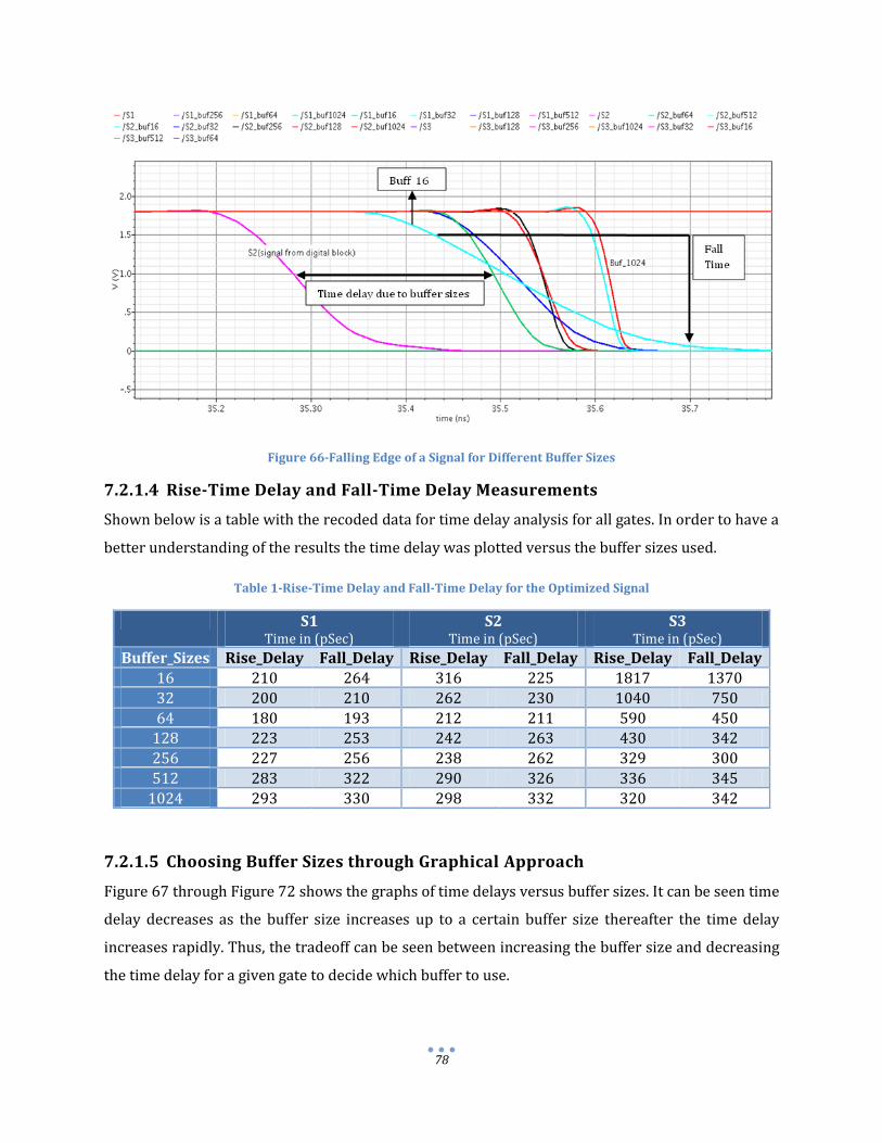
78
Figure 66-Falling Edge of a Signal for Different Buffer Sizes
7.2.1.4 Rise-Time Delay and Fall-Time Delay Measurements
Shown below is a table with the recoded data for time delay analysis for all gates. In order to have a
better understanding of the results the time delay was plotted versus the buffer sizes used.
Table 1-Rise-Time Delay and Fall-Time Delay for the Optimized Signal
S1 Time in (pSec)
S2 Time in (pSec)
S3 Time in (pSec)
Buffer_Sizes Rise_Delay Fall_Delay Rise_Delay Fall_Delay Rise_Delay Fall_Delay
16 210 264 316 225 1817 1370
32 200 210 262 230 1040 750
64 180 193 212 211 590 450 128 223 253 242 263 430 342
256 227 256 238 262 329 300
512 283 322 290 326 336 345
1024 293 330 298 332 320 342
7.2.1.5 Choosing Buffer Sizes through Graphical Approach
Figure 67 through Figure 72 shows the graphs of time delays versus buffer sizes. It can be seen time
delay decreases as the buffer size increases up to a certain buffer size thereafter the time delay
increases rapidly. Thus, the tradeoff can be seen between increasing the buffer size and decreasing
the time delay for a given gate to decide which buffer to use.

79
Figure 67-Plot of Rise Time Delays vs. Buffer Sizes for the Gate at the Sampling Capacitor
The graph above shows that the rise-time delay for NMOS gate at the output decreases to its
minimum for buff64 (log10 = 181) and rise-time delay (log10 = -9.74), which is the same result
observed in the simulations approach.
Figure 68-Plot of Fall Time Delays vs. Buffer Sizes for the Gate at the Sampling Capacitor
The fall-time delay for the same gate decreases to a lower value for buff 64 and fall-time delay (log10
= -9.71), again it is the same result observed in the simulation presented above.

80
Figure 69-Plot of Rise Time Delays vs. Buffer Sizes for the NMOS Gate at the Sampling Switch
The figure above displays the plot of rise-time delay vs. buffer size for NMOS gate at the CMOS
switch. In this case time delay reaches its minimum value for buff64 and rise-time delay (log10 = -
9.68).
Figure 70-Plot of Fall Time Delays vs. Buffer Sizes for the NMOS Gate at the Sampling Switch
The fall-time delay for the NMOS gate at the CMOS switch decreases to a lower value for buff 64 and
fall-time delay (log10 = -9.68), leading to a conclusion similar to the one presented above for the
particular gate.

81
Figure 71-Plot of Rise Time Delays vs. Buffer Sizes for the PMOS Gate at the Sampling Switch
The graph above displays the plot of rise-time delay vs. buffer size for PMOS gate at the CMOS
switch. This case results to a minimum time delay for buff256 (log10 = 2.41) and rise-time delay
(log10 = -9.48). It is an expected result since the gate size for a PMOS transistor is larger compare to
an NMOS transistor gate.
Figure 72-Plot of Fall Time Delays vs. Buffer Sizes for the PMOS Gate at the Sampling Switch

82
Figure 72 displays the plot of fall-time delay vs. buffer size for the same gate at the CMOS switch.
For this case the time delay for buff256 (log10 = 2.41) and rise-time delay (log10 = -9.52) is the
shortest time delay. Yet, considering that the decrease in time delay from buff128 to buff256 is only
0.42E-10 (from the table), it seems that buff128 is a better tradeoff since its physical size of buff128
is half the size.
7.2.2 LAYOUT OF SAMPLE AND HOLD BUFFERS There were many special considerations when completing the layout of the sample and hold buffers
due to the enormous sizes of the sample and hold MOSFET’s. The biggest considerations were due
to the large current spike needed when the tapered buffers were tripped. To take this into account,
very large power and ground metal runs were inserted to achieve a low enough resistance allowing
for sufficient switching speeds. Figure 73 shows the layout of the input tapered buffers. The large
metal run that wraps around the top of the circuit is the power and the large run in the middle of
the circuit is the ground connection. From these connections there are smaller spokes that connect
these larger powers to the individual tapered buffers.

83
Figure 73- Layout of Sample and Hold Buffers
VDD
VSS

84
7.3 DRIVING TRANSISTOR GATES AT CAPACITOR ARRAY Another crucial block of the digital design involved creating logic circuitry to drive the transistor
gates in the switched capacitor array based on the comparators’ outcome, a capacitor select signal,
and a residue mode signal. Signals that represent the comparators’ outcome and the capacitor
select are on-chip signals, whereas residue mode signal is an off-chip signal coming from an
external source such as an FPGA device. As shown below at Figure 74 each comparator’s outcome
is assigned a grey code value that represents one of the four outcomes to be considered, whereas
the rest of the combinations are ignored. Also, four possible logic combinations for the capacitor
select signal and residue mode signal are shown in the truth table,

85
Table 14 that follows below. In other words, based on the combination of the input signals,
comparators’ outcome and capacitor-select/residue-mode, output signals are generated that drive
eight assigned transistor gates at the capacitor array for forming one of the five output decisions of
the residue amplifier.
7.3.1 IMPLEMENTING RESIDUE AMPLIFIER DECISIONS Shown below is the matching of the comparators’ outcome to the residue amplifier decisions based
on the input signals described above. Notice that the solid arrow represents the residue -mode
signal that selects decisions -2, 0, and +2, whereas the dashed arrow represents the residue-mode
signal that selects decisions -1 and +1.
Figure 74- Matching of Comparators’ Outcome to Residue Amplifier Decisions
The truth table shown below is used to implement the functionalities described above. The truth
table was derived by considering all possible combinations of the variables described above.

86
Table 14-Truth Table for Gate Driver Digital Block
CAPACITOR-SELECT/RESIDUE-MODE COMBIANTIONS
Comparators’ Outcome
00 01 10 11
000 10101010 10101010 11111111 11111100
001 10101010 10101010 11110000 11111100
011 10101010 10101010 11110000 11000000
111 10101010 10101010 00000000 11000000
ELSE 10101010
Outputs, Transistor Gates
7.3.2 EXAMPLE OF A DECISION IMPLEMENTATION In order to further understand the complex operation of the gate digital driver it may be helpful to
consider an example of a decision implementation. For instance, let’s derive the implementation of
a “+2” decision. Shown below is the capacitor array whose gates are to be driven by the digital
driver.
Figure 75-Capacitor Array Block

87
In order to realize a “+2” decision the comparators output should be “111” and the capacitor-
select/residue-mode combination must be “10”, which means that capacitor-select signal allows the
capacitor array to perform its functions and residue-mode selects the “+2” decision. From the truth
table it can be seen that for the given comparators’ output, “111” and capacitor-select/residue-
mode combination “10” the signals to be sent to eight transistor gates are “00000000” with the far
left being the signal sent to the first gate, gate<0>. Going back to the capacitor array circuit and
assigning to each gate from gate<0> to gate<7> the corresponding bit, it can be seen that all PMOS
transistors will be “on” and all NMOS transistors will be “off”. This configuration connects all the
capacitors to the positive reference values, vrefp, thus giving rise to the “+2” decision. In addition,
by applying all combinations in the truth table to the capacitor array block one can realize all five
residue amplifier decisions.
7.3.3 FINAL STEP IN DESIGNING THE GATE DIGITAL DRIVER Once the truth table was created a hard ware description language (HDL) script was written in
VHDL using a digital designing graphical user interface (GUI), Xilinx 10.1i. Moreover, once the code
was written a test bench wave form was performed to verify the functions above. In this project, as
mentioned above, Cadence ICFB is used as the design tool. Yet, Cadence’s digital environment does
not support VHDL code; it supports Verilog instead. In order to use the written VHDL code an
intermediate path is followed. Cadence has the capability of converting a VHDL code to Verilog
code, which in turn is then synthesized using the available digital complier. For all the steps from
writing a VHDL code in Xilinx to completing the digital design in Cadence a tutorial was written.
After the designing process was completed the necessary power supply pins (VDD, VSS) were
attached to the digital component and a symbol was created for a simpler representation. The
newly digital driver was stored in a library for later use in circuit; its symbol representation is
shown below.
Figure 76-Digital Transistor Gate Driver

88
7.3.4 LAYOUT OF THE GATE DIGITAL DRIVER
The goal of the layout of the Gate Digital driver was to create the most compact solution possible. To do so all MOSFETS were put next to
each other in a linear fashion and connected together in a way where all the even metal layers traveled up and down and all the odd metal
layers traveled right to left. This allowed for a more dense solution as seen in Figure 77 below.
Figure 77- Layout of the Gate Digital Driver

7.4 DRIVING TRANSISTOR GATES OF INPUT-OUTPUT CAPACITORS OF RESIDUE AMPLIFIER This section concerns a digital block that drives the gates of switches that allow connecting
capacitors to the residue amplifier. The graphical behavior of the block is represented below
through the timing diagram. In this block the only external input controlling signal is the capSelect
signal, whereas the vresoutBuf signal is an output delayed signal that is feed back as an input to the
digital block. Delays between signals vresout and vresoutBuf, and vresin and vresinBuf are realized
through buffers as shown in circuit schematic representation below the timing diagram. The
functionalities of the digital block in discussion are as follows. When capSelect signal goes high
vresout switches to low in order to turn on the gate of the PMOS transistor leading to the connection
of Cout to the residue amplifier. Then, vresin goes high which in turn turns on the NMOS transistor
leading to the connection of Cin to the amplifier. On the other side, when capSelect goes low the
reverse operations take place. First, the capacitor Cout is disconnected followed by the disconnection
of Cin.
Figure 78-Behavior of “vresin-vresout switch” Digital Block
Below is shown an artistic circuit schematic representation together with the pins that connect to
the digital block described above.

90
vresin
vresinBuff
Residue Amplifier
m*Buffn*Buff
vresout
Cin Cout
vresin
vresoutBuff
capSelect
Figure 79-Representation of Gates to Drive With “vresin-vresout switch” Digital Block

91
7.5 DESIGNING “GENERICDEMUX” A demultiplexer (in this design called genericDemux) was another digital sub circuit designed with
the purpose of driving specific transistor gates based on certain input signal combinations. The
inputs of this digital block driver are the input to be send to a selected output pin, and the output
pin select signal. For each case two variables are considered, which give rise to four possible input
combinations. Yet, for this application only two combinations are needed for each case; the rest are
used to set the output values to zero “low” values. In the tables below the left columns represent
the input signal combinations and the right columns show the output results. On the left column the
bit on the far left corresponds to the input signal, whereas the bit on the right represents the select
output pin signal.
Table below shows the relationship between the input-select signal and output1 pin.
Table 15- input/output1 Relationship for “genericDemux”
input-select output1
00 0
10 1
ELSE 0
The following table represents the relationship between the input-select signal and output2 pin.
Table 16- input/output2 Relationship for “genericDemux”
input-select Output2
01 0
11 1
ELSE 0

92
7.5.1 “GENERICDEMUX” SYMBOL REPRESENTATION After the logic behavior of the demux was established a VHDL script was written in Xilinx and
synthesized in Cadence’s digital designing tools. A symbol representation of the demultiplexer
circuit was created and the newly designed digital driver was tested to verify its proper
functionalities. Below is shown the symbol representation of this digital block.
Figure 80- “genericDemux” Symbol Representation
In order to verify the demultiplexer’s proper functionality a simulation test was performed. For
instance, let’s consider an input combination from the truth table that represents the relationship
between input/output2, and observe the output. Shown in the graph is a doted arrow that shows
the input combination of input-select as “11”. For this input combination the expected outputs
(from the truth table) are output1 “0” and output2 “1”. Moreover, by following the same procedure
one can verify that the designed demux implements all logic combinations described in the truth
tables above.

93
Figure 81-Results “genericDemux” Simulation
7.5.2 LAYOUT OF THE DIGITAL BLOCK Figure 82 below shows the layout of the Generic demultiplexer using two transistors.
Figure 82- Layout of Generic Demux

94
8 THE COMPARATORS
The Cyclic ADC uses 3 comparators to create the digital decisions. The comparators are connected
to the output of the residue amplifier and are arranged in a thermometer code. The comparators
consist of the preamps, which are used to set the decision levels, amplify the difference between the
inputs and set the proper input voltage for the analog latch. The analog latch uses two inverters
that are connected to each other in a positive feedback configuration and are kept at their
metastable point until nudged by the output of the preamplifier to trigger the latch. The final
component in the comparators is the digital latch. The digital latch holds the value of the decision
throughout the next cycle and buffers the output to drive the external FPGA.
8.1 THE PRE-AMPLIFIERS There are two designs for the preamps. One design compares Voutp directly to Voutm and amplifies
there difference this is used in the “0” comparator. The other preamplifier design is used in the
“+1” and “-1” comparators to evaluate Voutp to Voutm+0.34V. This comparator is used to see if the
difference of Voutp to Voutm is greater than ½ Vref .
8.1.1 THE ±1 PREAMP The ±1 preamp is used to compare 1.47V to 1.13V and amplify the difference between the inputs.
Figure 83 shows a schematic representation of preamp. Some issues that arose in the making of
this preamp was the fact that the voltage difference of the output is less than the Vth of the
MOSFET’s , the input voltage is centered at 1.3V and, the output voltage needs to be centered at
around 0.9V.

95
In order to create an imbalance in the preamplifier decision levels an intentional mismatch was
created in the differential pair and also a mismatch in the source followers. With an input of 1.47V
for Vinp and 1.13V Vinm , the source followers reduce this voltage mismatch and lower the common
mode voltages to 770mV and 600mV. This leaves 170mV of mismatch to be compensated for by
the differential pair. Like the source followers, the Diff pair is mismatched. The differential pair
uses a self biased active load to have high output impedance and was biased with a replica bias that
was set to the comparator threshold voltage on the input. In order to keep the voltage threshold of
the comparators stable, the bias current of the replica was set by comparing the output of one leg of
the replica bias circuit to 0.9V using a differential pair current amplifier. One issue that was found
with using a feedback loop was that there were two stable states in which 0.9V could be achieved.
One state is when there is 50µA going through the circuit and the other state was when the system
was barely on and there was only pico amps of current flowing through it. To mitigate the two
stable states a constant 35µA bias current is used in addition to the replica bias transistor creating
only one stable state of 50µA.

Figure 83 - ±1 Preamplifier

Figure 84-Figure 86 below shows the startup transient of the replica bias circuitry. The first plot in
each figure shows the gate voltage of Vbias. This voltage is set by the negative feedback amplifier.
The second plot in each figure shows the convergence of Vrep1 and Vrep2 as the startup transients of
the preamplifier dies out. The third plot in each figure shows the current through the differential
amplifier.
Figure 84- Startup transient 27˚ C of ±1 Preamp
Figure 84 shows that the startup transient of the preamp at 27˚ C takes about 2.75µs to converge
and differential amplifier uses about 54uA.
Figure 85- Startup Transient at 70˚C of ±1 Preamp

98
Figure 85 and Figure 86 shows that the startup transient of the preamp at 70˚ C takes about 2µs to
converge and differential amplifier uses about 34uA. Also due to the high temperature there is a
small output offset not seen in the 27˚C simulation.
Figure 86- Startup Transient at 0˚C of ±1 Preamp
Figure 86 shows that the startup transient of the preamp at 0˚ C takes about 12µs to converge and
differential amplifier uses about 70uA. Also due to the low temperature there is a small output
offset not seen in the 27˚C simulation.
Figure 87 - Dc sweep of ±1 Preamp

99
Figure 87 shows a DC sweep of the ±1 preamplifier. There is a 340mV differential offset on the
preamplifier which is used to set the decision level of the comparators. The gain of this
preamplifier at 170mV single ended (zero crossing of output) is 35.1𝑉
𝑉 as seen in Figure 88. Unlike
in the successive approximation analog to digital converter where the preamplifiers need to have a
high gain and low noise, the cyclic ADC can recover from decision errors in the next residue cycle.
Figure 88- Preamplifier DC Gain Plot

8.1.1.1 Layout of the ±1 Preamplifier
Figure 89 below shows the layout of the ±1 preamplifier including the two capacitors to prevent oscillations in the bias circuit in the preamp.
Figure 89- Layout of the ± 1 Preamplifier
8.1.2 THE 0 PREAMP The zero preamp is used as the middle comparator in the thermometer code. The comparator
schematic is shown in Figure 90 and is much simpler than the ±1 comparator due to the fact that
there does not need to be any intentional mismatch between the inputs of the differential pair or
the source followers. This differential pair is also actively loaded with a self biased load to assure
simple and effective biasing. The length and width of the transistors was determined by finding the
proper ratio to allow for a 0.9V output common mode voltage. To keep a stable bias over input
range, a replica bias was used that mimics the entire circuit which keeps the drain to source
voltages on the biasing transistors equal which creates a much better current mirror.

Figure 90 –Preamplifier for the Zero Comparator

8.1.2.1 Layout of the Zero Preamplifier.
Figure 91 below shows the layout of the zero preamplifier, when creating this layout, much care was taken to compensate for mismatch
errors using the common centroid layout.
Figure 91- Layout of the Zero Preamplifier

Figure 92 below shows a DC sweep of the preamplifier for the zero comparator. The maximum gain
of this circuit is 32.1𝑉
𝑉 , this occurs at 0V differential input as seen below.
Figure 92- DC plot of the Zero preamp
8.2 ANALOG LATCH The analog latch employs positive feedback to take the differential output from the preamplifiers
and to amplify it until the differential output hits the rails. The circuit is built by using two
inverters connected in a positive feedback configuration that is clamped with 2 PMOS transistors.
This inverter configuration is then nudged by a differential pair with inputs connected to their
corresponding preamplifier. Figure 93 shows the actual schematic of the analog latch that was
borrowed from Cody Brenneman for use in a self calibrating successive approximation ADC.

Figure 93- Analog Latch

8.2.1 LAYOUT OF THE ANALOG LATCH The layout of the analog latch was completed by Cody Brenneman and was specifically designed to have a low parasitic capacitance in
order to reach the rail as fast as possible.
Figure 94- Layout of the Analog Latch

8.3 DIGITAL LATCH This project makes use of 2 different types of digital latches a latch that when reset holds a “0” state
and a latch that resets to a “1” state. This is used to set the logic levels for the first conversion cycle
when a zero decision needs to be made. The thermometer code for the comparators needs to be
“001” to create a zero decision. The digital latch was created using the basic D-flip flop topology and
adding logic to create a “1” state when the reset input is high. To create a “0” resetting latch, the
outputs Q and Qbar were switched and an input inverter was used to invert the signal to negate the
Qbar output. In order to sample only on the rising edge of the clock, 2 delay blocks and an inverter
were placed in the circuit to create a race condition to the and-gate as seen in Figure 95. The
schematics of the “1” and “0” reset latches are shown in figures Figure 96 and Figure 97
Figure 95- Rising edge detector

Figure 97- Digital Latch with "1" Reset
Figure 96- Digital Latch with “0” Reset

8.3.1 LAYOUT OF THE DIGITAL LATCHES Figure 98 andFigure 99 below shows the layout of the digital latches used hold the output of the analog latch for the next cycle.
Figure 99 - Layout of Digital Latch with Minus Reset Figure 98 – Layout of the Digital Latch with Plus Reset

8.4 PUTTING IT ALL TOGETHER Once all the separate sub-systems were built, a new schematic was made that incorporated all the
blocks and the appropriate connecting circuitry. A symbol was then made to be used in the top level
schematic as seen in Figure 100.
Figure 100 - "+1" Comparator Symbol
Whole block simulations were done to assess the operation and to test the accuracy of the
comparator threshold voltages and the timing of the input signals. A transient simulation was
completed in Figure 102 using the “+1” comparator and a 240mV input signal. This caused a low
decision by the comparator due to its 340mV threshold for a high logic level.

Figure 101 – Schematic Block Diagram of Comparators

Figure 102- Transient Simulation of +1 Comparator using a 280mV differential input
The first simulation in Figure 102 shows the transient response of the preamplifiers firing at 10ns.
At 17ns the analog latch is released as seen in the second simulation causing the preamp settling to
have a ripple in it due to the parasitic capacitance to the drain and source of the gates of the
MOSFET’s in the analog latch injecting charge into the output node of the preamps. The third
simulation shows the output of the block, the digital latch transitioning at 21ns. The fourth
simulation shows the control signals used to trigger the comparators.

8.4.1 LAYOUT OF COMPLETE COMPARATORS Once the appropriate sub blocks were created and laid out, the complete comparator block needed
to be connected. This was accomplished by connecting the sub blocks together in a compact fashion
taking into account the interconnections and power routing between the various blocks. Figure
103,Figure 104 and Figure 105 below shows the “+1” Comparator, “0” Comparator and the “-1”
Comparator respectively.
Figure 103 - Layout of “+1” Comparator

114
Figure 104 - Layout of "0" Comparator
Figure 105- Layout of the "-1" Comparator

115
THE BIAS BLOCK
The goal of the bias block is to create as close to an ideal current source as possible using CMOS
transistors. In an ideal current source, the output resistance of the source in infinite and the current
is constant no matter what the voltage is across the source. When a MOSFET is operated in the
active region, the MOSFET behaves like a current source with its output resistance being dependent
of the channel length modulation parameter λ. This parameter λ is due to the fact that pinch off of
the channel is occurs when the MOSFET is operating in the active region. As the drain to source
voltage is increased, the pinch off point moves towards the source causing the channel length to be
shorter than the physical length of the MOSFET. In short channel transistors this channel length
modulation becomes is a sizeable portion of the total length of the MOSFET increasing the output
current dependency of the drain to source voltage. To combat this, the length of the MOSFET’s in
the current mirror was increased from the standard 0.18µm set by the process to a much larger
1µm. To further increase the output resistance of the bias current source, a cascode is used to
shield the MOSFET’s in the current mirror from the varying voltages the current source
experiences.
Figure 106- Bias Block schematic
NMOS Current Sources
PMOS Current Sources
Isolated Diff
Pair Current
Source

116
8.5 PROBLEMS WITH BIAS BLOCK One of the biggest issues that were encountered when building the bias block was the crosstalk
from the residue amplifier. Since the residue amplifier is an open loop amplifier the only thing that
holds the amplifiers inputs at the common mode voltage is the common mode rejection of the
amplifier through many cycles of the amplifier. In the first few cycles of the conversion the inputs
of the differential pair are not at the proper input common mode. This puts a strain on the bias
circuit by changing the drain to source voltages on the bias circuits causing a large change in the Vds
of the cascoded MOSFET’S. Since the total width of the cascoded MOSFET for the differential pair is
122µ there is a large gate to drain capacitance. This capacitance couples the changing drain voltage
of the differential pair current source to the cascode gate voltages causing crosstalk between all the
currents in the IC. To prevent this, the bias current for the differential pair was isolated as seen in
Figure 106 by using separate 0.9V cascode voltages for the differential pair and the rest of the bias
block.
8.6 RESULTS OF ISOLATION Figure 108 below shows the crosstalk between the differential pair current source voltage to the
voltages at all the other current sources. The largest perturbation of the bias current in the
differential pair occurs during the first cycle when the input voltages in the differential pair are not
centered on the input common mode. When this occurs the bias current voltage swings 200mV
which gets coupled onto all the bias signals which disturbs the current in the entire IC. Figure 107
below shows the effectiveness of the isolation circuit. Any perturbation in the differential pair bias
current does not affect the currents in the entire IC.
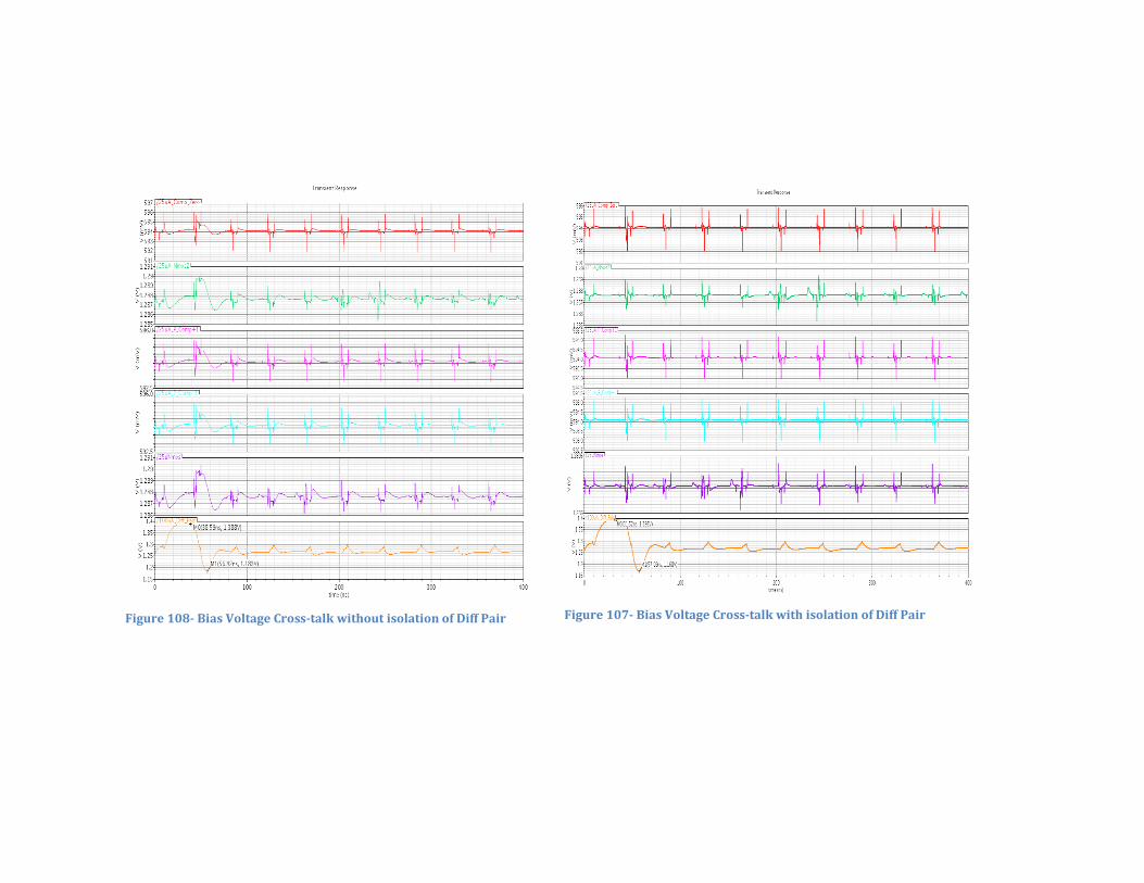
Figure 108- Bias Voltage Cross-talk without isolation of Diff Pair Figure 107- Bias Voltage Cross-talk with isolation of Diff Pair

8.7 LAYOUT OF THE BIAS BLOCK When creating the layout of the bias block special consideration was taken to create a mirrored
layout to reduce the effect doping gradients. To do this a half bias block was created that produced
half the current need for each reference bias. Once completed a larger bias block was designed
using the two half blocks as seen in Figure 109 below. The two 25kΩ resistors seen in the
schematic below are used to provide the 0.9V cascode voltage for the isolated differential pair.
Figure 109- Full Bias Block Schematic

Figure 110 below shows the completed bias block layout including the two half bias blocks and the differential pair cascode resistors.
Figure 110- Full Bias Block Layout
Half Bias Block 1
Half Bias Block 2
Cascode resistors voltage divider

9 THE OUTPUT BLOCK
One of the issues that were originally discussed during the MQP was how to drive the digital
outputs of the ADC. To do this, as represented in the background section, a common method known
as Low Voltage Differential Signaling (LVDS).This block would follow the comparator logic block, as
the diagram below indicates.
Figure 111- Block Interaction between Logic and Output Drivers

121
9.1 CREATING LVDS DRIVERS After performing research, the specifications of the industry standard LVDS was found as seen in
the table below:
Table 17 - LVDS Standards
Standard Min Max
Voltage Across Resistor 350mV 247mV 454mV Common Mode Voltage 1.2V 1.125V 1.375V
Current 3.5mA
Output Resistor 100Ω
Shown below is a copy of Figure 18. In this particular case, the receiver would be an FPGA that is
capable of taking LVDS outputs, which usually requires some signal translation.
Figure 112 - LVDS Revisited: Theoretical Schematic
To bias the LVDS, an N-MOS current mirror, with values designed to match the desired 3.5mA in the
specification. Also, the size of the transistors were set to allow for the 1.2V common mode. This
schematic is shown below:

122
Figure 113 - LVDS Schematic: Actual Circuit Implementation
As can be seen above, there is a transmission gate (M8, M23) at the input, which is fed by an input
voltage. This value is then obtained by the 4 transistors (M0, M1, M3, M4) forming the LVDS driver.
The biasing for the transistors is done by a simple current mirror (M17, M18). R3 is the output
resistor, with a parasitic capacitor next to it. To confirm that the circuit was running a transient
analysis was performed in ICFB. The results of that analysis are shown below:

123
Figure 114 – Simulated LVDS Outputs
From the top: (1) as can be seen, the current stays constant at 3.5mA. (2) The input voltage is
shown as a piecewise linear function. (3) Differential counterpart to input. (4) Differential voltage
seen by the receiver.
Figure 114, proves that all standards outlined in Table 17 have been met. Therefore the LVDS is
ready for use.

124
9.2 MAKING THE CHOICE BETWEEN LVDS AND LVCMOS Although a working version of an LVDS driver was created, it was necessary to analyze if creating
these drivers would be a worthwhile effort for this project. Therefore, the chart below was created:
Table 18 - LVDS and LVCMOS Comparison
Specification LVDS LVCMOS Preference
Number of Wires
12 6 LVCMOS
Complexity The design of a driver that can adhere to LVDS standards is necessary, which adds high complexity, comparatively.
Simple MOSFET drivers with common voltage references within the circuit
LVCMOS
Noise Reduces noise in long wire distances by being differential, especially in higher frequencies.
More prone to noise in longer distances, due to jitter and interference in system
LVDS
Power Moderate Power, Low Power LVCMOS Transmission Serial or Parallel Parallel LVCMOS
Speed Accommodates very high frequencies. Less used for high frequencies
LVDS
The table above shows a contrast between the two most feasible options: LVDS, being a great
technology in high-speed applications that require low noise levels, and LVCOMS, being the simpler,
more trivial option. Due to the complexity of this project it was determined that LVCMOS would
use less power, less output pins and would be less complex to implement. In order to make LVDS a
more convincing choice, circuitry would have to be added to serialize the data and transmit the 3
bits on one differential line. Since the data rate of LVCMOS is sufficient to transmit the parallel
comparator thermometer codes and would only use one more pin than the serialized LVDS data,
LVCMOS was ultimately chosen.
9.3 OUTPUT PROCESS Due to the fact that LVCMOS will be used and will be sent to the FPGA, some the following
characteristics apply to this block:
Output will be a thermometer code
Output code will be given per cycle, not per conversion.
Output Buffers will be confined in each Comparator Block.

125
10 PUTTING IT ALL TOGETHER
As each individual blocks in the Cyclic ADC was created and verified, the top level schematic which
contained ideal components were replaced with the proper schematics. Once all the blocks were
created a full schematic simulation was attempted. It took numerous minor corrections to have all
the different blocks work together and create a conversion. One of the major issues encountered
was the many timing issues that needed to be fixed to compensate for the differences in the ideal
blocks and the actual schematics. Figure 115 shows the annotated full chip schematic below.

Figure 115 - Full Chip Schematic
Switched Capacitor 1
Switched Capacitor 3
Switched Capacitor 2
Switched Capacitor 4
Comparators
Input
Bias
Reference
Input Block Minus
Input Block Plus
Differential Pair
Digital Timing
Digital Timing

127
10.1 FULL CHIP SCHEMATIC SIMULATIONS Once the ADC was running and the comparators were outputting valid digital codes, a series of
complete simulations were done build enough data to create the residue plot. The residue plot was
found by comparing the output voltage of the previous cycle’s residue voltage to the output of the
differential pair after a decision was made. This collection of points was then grouped by the
decision level and plotted as seen in the figure below.
Figure 116- ADC Residue Plot with Unmatched Parasitics
Once Figure 116 was completed it became evident that there was a system wide problem in this
Cyclic ADC. It appeared that the only residue mode out of the 5 decision levels that was working
correctly was the “0” decision, all the other decisions had two residue plots coinciding with each
one. After seeing this phenomenon, more simulations were completed to see if this pattern was a
coincidence or was actually occurring. It became evident that this was not a measurement error in
the extraction of the data or coincidence but some unmatched element in the Cyclic ADC. To verify
this phenomenon, additional simulations were completed gathering data on the residue plot and
which switched capacitor circuit was completing the subtraction. After sufficient data was taken it
became evident that when the switched capacitors 1&3 as seen in Figure 115 were doing the DAC
implementation, the residue plot was pushed towards the 0V differential voltage compared to when
0 Decision
+1 Decision
+2 Decision
-1 Decision
-2 Decision

128
switched capacitors 2&4 implemented the DAC decision. This difference is noted in Figure 110
below with switched capacitor circuits 1&3 in red and switched capacitor circuits 2&4 in blue.
Figure 117- Residue Plot with Unmated Parasitics ( DAC 1&3 Red DAC 2&4 Blue)
Figure 117 suggested that the switched capacitor circuits 1 and 3 had an additional capacitance on
a sensitive node that was creating a capacitor voltage divider on the sample capacitors which was
reducing the voltage gain of the circuit. This phenomenon seemed improbable due to the
symmetrical nature of the cyclic ADC. As seen in Figure 115 the only block that was not symmetrical
that was connected to any sensitive nodes was the input block. Attached to the top plates of the
capacitors in the switched capacitor blocks 1 and 3 was a 454.5µm NMOS transistor connecting the
top plates of the sample capacitors to Vicm. To test if the parasitic capacitance of this NMOS
transistor was causing the discrepancy in the residue plot, an identical NMOS transistor was
connected to the top plates of the capacitors in the switched capacitor blocks 2 and 4 and the
residue plot was generated as seen in Figure 118.
0 Decision
+1 Decision
+2 Decision
-1 Decision
-2 Decision

129
Figure 118- Residue Plot with Matched Parasitics
After adding the identical NMOS transistor to switched capacitor circuits 2 and 4 that was attached
to the top plates of switched capacitor circuit 1 and 3, the residue plots converged to one line from
each decision. This addition of the NMOS transistor proved that the source of the discrepancy was
due to the additional parasitic capacitance the input MOSFET put on the sensitive node. This
discovery opened up a series of questions on the feasibility of the entire design and a way to
calibrate for the differences in the 2 DAC’s in the current design.
0 Decision
+1 Decision
+2 Decision
-1 Decision
-2 Decision

130
10.2 LAYOUT OF COMPLETED ADC Once the full chip simulation was completed and verified, the layout of the ADC began in blocks
beginning with the Differential pair. Once the layout of a block was completed, verified using a
design rule check (DRC) and a layout verse schematic check (LVS) the block was simulated to verify
its functionality and then the next block was laid out. The DRC check is designed to verify layout
rules from the semiconductor foundry to insure accurate fabrication of the integrated circuit. One
example of this is the metal spacing rule. Due to mask errors, there is a minimum distance that two
metal runs can be away from each other. If this design rule is not abided, there is a possibility that
the two separate metal runs would be shorted together. The layout verse schematic check is
designed to verify that the schematic and the layout match. One example of a LVS error is if there is
a missing metal run between two transistors in the layout that is in the schematic. The LVS check
will help narrow down the location of the mismatch and verify if has been corrected.
Figure 119 shows the completed layout of the Cyclic ADC including the split feature. As can be seen
below there are two half ADC’s that are combined in the figure below. Due to the fact that this ADC
was not going to be fabricated because of the inherent flaw with using the differential pair, the pad
ring was not completed which would have been designed for a 2.5mm by 2.5mm package while this
chip is approximately 590um by 438um. This would have led to an extremely long power and
ground lines that is unnecessary. Because of the lack of a pad ring and locations for the power and
ground the very top level routing was not designed and was simulated using the schematic only.
Figure 120 shows an exploded view of a fully labeled half ADC.

131
Figure 119- Completed ADC Layout
A D C 1
A D C 2

132
Capacitor 1 Capacitor 2
Logic
4
INPUT BLOCK
Input Buffers
Capacitor 3
Capacitor 4
Logic
1
Logic
2
Logic
3
Diff Pair
Comparator +1
Comparator -1
Comparator 0
Bias
Timing
Figure 120- Half ADC Labeled Layout

133
10.3 EXTRACTED SIMULATIONS OF THE COMPLETE ADC After completing individual simulations on all blocks in the ADC laid out, a full extracted simulation
was completed and a residue plot was created. An extracted simulation is a simulation that uses the
layout of a circuit to recreate a schematic. This new schematic includes variables from the layout
such as trace resistances and parasitic capacitances. The extracted simulation accounted for
parasitic resistances greater than 10mΩ and parasitic capacitances greater than 1fF this resulted in
a total of 900 NMOS MOSFET’s, 1290 PMOS MOSFET’s, 35780 Capacitors and 9480 resistors.
Figure 121 shows the completed residue plot of the full scale extracted simulation. This figure was
found by completing many transient simulations varying the input voltage and tracking the
capacitor voltages and decisions over each cycle.

134
Figure 121 - Residue Plot of Full Scale extracted simulation of the Cyclic ADC

135
11 NOISE ANALYSIS
One of the most important performance metrics of an ADC is its noise performance. As discussed in
the input block, the best noise performance that can be attained in an ADC is determined by its
KT/C capacitor noise. The goal of this section is to characterize the noise performance of the
residue amplifier and to modify the residue amplifier to achieve a sufficient noise performance for
this ADC.
The schematics below shows the Differential Pair and the switched capacitor circuit being analyzed.
The components that need to be analyzed in the in the amplifier circuit include the differential pair,
a resistive load and the replica bias. In the switched capacitor circuit the main components that
need to be analyzed is the CMOS transmission gate that connects the output of the differential pair
to the top plate of the capacitors in the switched capacitor circuit and also the PMOS switches that
connect the bottom plate of the capacitors to the output common mode.
11.1 CIRCUIT SCHEMATIC Figure 124 below shows the complete schematic of the differential pair including the
MOSFET’s responsible for shorting the inputs and the outputs to their respective common modes.
Figure 125 shows the complete Switched capacitor network including the MOSFET’s used in other
parts of the ADC conversion cycle. Figure 126 is a simplified schematic of Figure 123 and Figure
125 and removes all MOSFET’s are off during Residue amplification process.

136
Figure 124- Differential Pair Figure 125- Switched Capacitor Block
Figure 126- Simplified Full Residue Amplifier Schematic

137
11.2 BANDWIDTH OF RESIDUE AMPLIFIER The Bandwidth of the residue amplifier is limited by the parasitic capacitances and
resistances of the MOSFET’s. In order to accurately find the bandwidth of the entire residue
amplifier, a simulation was run on the entire amplifier circuit and a bode plot was generated as
seen below.
Figure 127- Bandwidth of Residue Amplifier
The blue trace in Figure 127 shows the magnitude of the frequency response of the differential pair
and the red trace shows the output to the top plates of the capacitors. The DC gain of the residue
amplifier is 4.7db, the bandwidth of the differential pair is 1.48 GHz and the bandwidth of the entire
residue amplifier is 342 MHz. Since the bandwidth is limited by the voltage on the top plates of the
capacitors, the total noise will be integrated by the noise bandwidth of 23.177 ∗ 103 𝐻𝑧.
Noise Bandwidth = π
2∗ F3db
Noise Bandwidth = π
2∗ 342 Mhz = 23.177 ∗ 103 𝐻𝑧

138
11.3 NOISE IN THE DIFFERENTIAL PAIR There are 3 noise sources that are taken into account when analyzing the residue amplifier,
Thermal noise, Shot noise and 1/f noise. In order to accurately model the total noise of this system,
simulations spice simulations must be run.
11.3.1 RESISTOR NOISE There are two 500Ω resistors that act as the load in the differential pair, each contributing
equal amounts of noise. Since each resistor is directly connected to the output of the differential
pair the gain seen by each resistors noise is one.
𝑅𝑒𝑠𝑖𝑠𝑡𝑜𝑟 𝑁𝑜𝑖𝑠𝑒 = 4 ∗ 𝐾 ∗ 𝑇 ∗ 𝑅
𝑅𝑒𝑠𝑖𝑠𝑡𝑜𝑟 𝑁𝑜𝑖𝑠𝑒 = 4 ∗ 1.38𝐸−23 ∗ 290𝑘 ∗ 500Ω = 2.829𝑛𝑉
𝐻𝑧
11.3.2 REPLICA BIAS NOISE The replica bias circuit employed in this circuit is used to increase the common mode
rejection ratio of the differential pair. The increases the accuracy of the current mirror by
mimicking the drain to source voltage that current source of the differential amplifier sees. Any
noise from the replica bias or the current mirror will result in noise in the differential pair bias
current. In an ideal case, the differential pair and the load resistors would be perfectly matched
resulting in zero gain of the current noise to the output, making the noise in the replica bias
irrelevant. In a real integrated circuit imperfect matching and gradients in doping would create a
path for the bias current noise to affect the output of the amplifier. To minimize this effect a
common centroid layout was used in the differential pair. The common centroid layout is a
technique used to cancel out first order doping gradients in any direction for two identical
MOSFET’s. Figure 128 below shows the common centroid layout. Given two MOSFET’s M1 and M2
that need to be matched, each MOSFET can be split into 4 separate MOSFET’s and arranged in the
configuration below. Assuming good matching in the differential pair, any noise in the replica bias
circuit would be attenuated significantly by the symmetry of the circuitry and the differential
nature of the integrated making the noise added by any of the bias circuitry to be insignificant.
M1.1
M2.1
M1.3
M1.2
M2.2
M2.3
M2.4
M1.4
Figure 128- Common Centroid layout technique for two MOSFET’s

139
11.4 NOISE SIMULATIONS USING CADENCE The process that is being used to design this ADC is the Jazz 0.18µ CMOS process. In order to
properly model the various noise parameters, a noise simulation in ICFB must be run. To get valid
results the model files that simulate the properties of the CMOS process includes various noise
parameters. In order to get a baseline for my circuit I ran a noise simulation on the differential pair
using an ideal current source as seen in figure 6 below.
Figure 129- Differential Pair with Ideal Current Source

140
11.5 1/F NOISE Figure 130 below shows the noise simulation of the differential pair. There is a very large
1/f noise region. 1/f noise is caused by imperfections in the lattice atoms of the silicon wafer and is
increased as the channel length of a MOSFET is decreased. It is clear in the figure below that 1/f
noise dominates the noise performance in frequencies up to 100 Mhz.
Figure 130- Noise Simulation of Differential Pair with Ideal Current Source
In order to reduce the 1/f noise the channel length of the MOSFET’s in the differential pair must be
increased. Below shows a simulation of the 1/f noise for a 10x increase and a 100x increase in
MOSFET Length while keeping the W/L ratio constant.

141
Figure 131- Noise Simulation of Differential pair with 10x Lengths
When the length of the MOSFET’s in the differential pair was increased by a factor of 10x as seen in
Figure 131, the high frequency cutoff of the 1/f noise was reduced to 400khz and the bandwidth
was reduced by a factor of 10x.
Figure 132- Noise Simulation of Differential Pair with 100x Lengths

142
When the length of the MOSFET’s in the differential pair was increased by a factor of 100x as seen
in Figure 131, the high frequency cutoff of the 1/f noise was reduced to 30 kHz and the bandwidth
was reduced by a factor of 100x.
11.6 CHOOSING THE LENGTH OF THE MOSFET’S As the length of the MOSFET’s in the differential pair were increased, the 1/f noise and the
bandwidth decreased linearly. Since the bandwidth of the differential pair is much higher than that
of the switched capacitor circuit, the bandwidth of the differential pair can be reduced without
affecting the bandwidth of the entire circuit. After noting the linear relationship between
bandwidth and channel length, it appears that the channel length can be optimized to provide the
lowest 1/f noise possible while having sufficient bandwidth.
11.7 INCREASING BIAS CURRENT Once the channel length is optimized to provide the lowest frequency at which the 1/f noise
is dominant, the bias current can be increased to further reduce the total noise of the circuit by
lowering the entire noise plot. If the total power was increased by a factor of four, then each load
resistor would be reduced to 250Ω while leaving the gain constant as seen by factor of four increase
in transconductance.
𝑔𝑚 = 2𝐼𝑑
𝑉𝐺𝑆 − 𝑉𝑇
4 ∗ 𝑔𝑚 = 4 ∗ (2𝐼𝑑)
𝑉𝐺𝑆 − 𝑉𝑇

143
11.8 NOISE MODELING OF ACTUAL DIFFERENTIAL PAIR Using the experimental simulation data found in the previous section the noise of the complete ADC
Differential pair could be optimized. First a baseline noise simulation was run on the Differential
pair in Figure 122 and the Switched Capacitor Circuit in Figure 123.
Figure 133- Power Spectral Density of Original Differential Pair
As seen in Figure 133 the noise from the amplifier is 344uV RMS. Variance was determined by
taking the integral of the graph above in Matlab.
Figure 134- Power Spectral Density of Switched Capacitor Circuit

144
As seen in Figure 134 the noise of the switched capacitor circuit is 47.8uV which is mostly due to
KT/C noise as compared to ideal KT/C noise which has 44.7µV of noise. The extra 2.9uV of noise is
due to the modified switched capacitor circuit with MOSFET switches on the top and bottom plates
of the capacitor as seen in the figure below.
Figure 135- KTC Capacitor Noise (Left) - KTC Modified Capacitor Noise (Right)
After breaking up the Circuit into 2 sections it became clear that the only circuit that needs to be
modified to reduce the total noise is the Differential Pair amplifier circuit. From the experimental
results of the first section the length of the MOSFET’s in the differential pair was increased from
180nm to 18um and the width of the MOSFET’s was increased to 2mm. A noise simulation was then
completed to monitor the noise improvement.

145
Figure 136 above shows the reduction of the 1/f noise from the 100x increase in width of the
differential pair MOSFET’s. The noise total noise of the differential pair circuit has been reduced to
132uV RMS from 344uV RMS. To further decrease the noise in this circuit the bias circuit was
increased by a factor of four.
Figure 136- Power Spectral Density of Differential Pair with 100x MOSFETS
Figure 137- Noise Simulation of Differential pair with Large MOSFET’s and 4x bias current.

146
The increase in bias current from 1mA to 4mA decreased the noise of the complete differential
amplifier from 132uV to 82.7uV. Increasing the current by a factor of 4 decreased the noise to 62%
of the 132uV. Ideally increasing the current by a factor of 4 would make the noise be reduced to
50% of the total noise. This discrepancy is due to the other noise sources in the signal path such as
the noise from the MOSFET switches that connect the amplifier to the switched capacitor circuit
which is not affected by the increase in current through the differential pair.
11.9 TOTAL NOISE WITH MODIFIED CIRCUIT The total noise of the modified circuit as seen in the figure below is 72.8uV RMS. This is less than
double the absolute minimum noise due of 44.7uV RMS due to the KT/C capacitor noise.
The addition of the extra pole from the MOSFET adds another pole at around 1Ghz which
reduces the noise by an extra 20dB per decade after the pole frequency. This attenuation filters the
noise in the differential pair circuit making it only contribute 54.404uV of noise. This cascaded with
the 47.8uV is where the 72.42uV RMS of noise is created as seen in the equation below.
𝑇𝑜𝑡𝑎𝑙 𝑁𝑜𝑖𝑠𝑒 = 𝑆𝑤𝑖𝑡𝑐𝑒𝑑 𝐶𝑎𝑝 𝑁𝑜𝑖𝑠𝑒2 + 𝐷𝑖𝑓𝑓𝑒𝑟𝑒𝑛𝑡𝑖𝑎𝑙 𝑃𝑎𝑖𝑟 𝑁𝑜𝑖𝑠𝑒2
74.42𝑢𝑉 = 54.404𝑢𝑉2 + 47.8𝑢𝑉2
Figure 138- Power Spectral Density of the Full Residue Amplifier Circuit

147
11.10 FEASIBILITY OF REDUCING NOISE USING CURRENT TECHNIQUES Although the noise due to the differential pair and the KT/C capacitor noise contribute
almost equally to the total noise, the current method used to decrease the 1/f noise was to increase
the length of the MOSFET’s in the differential pair. When the length of the MOSFET’s were
increased, the width of the MOSFET’s needed to be increased proportionally making the total
MOSFET area increase in a squared fashion. Since the length and the width of the MOSFET were
increased by 100 the total die area was increased by 10,000. As this might be beneficial for noise
performance, it degrades almost all other performance metrics. As the area of the MOSFET
increases the gate capacitance all the parasitic capacitances increase linearly. This presents a
problem when using a switched capacitor circuit as the increase in gate capacitance creates a large
capacitor divider reducing the signal input voltage in the circuit. Also this increase in capacitance
reduces the speed of the MOSFET’s causing longer settling times reducing the overall speed of the
ADC.
11.11 OTHER WAYS TO REDUCE 1/F NOISE Since this ADC is running at 1Mhz and 200ns out of the 1µs is dedicated towards input
sampling in which time the ADC remains dormant, this time could be used to turn off the bias
current in the differential pair. Due to the fact that low frequency cutoff for 1/f noise is determined
by how long the MOSFET has been turned on, if the differential pair is reset every microsecond, the
low frequency limit for the 1/f noise would be limited to 1Mhz. The figure below shows the total
noise using MOSFET’s that are 10x longer than minimum length with the 1Mhz 1/f noise low
frequency limit.
1/f Noise Eliminated
Figure 139- PSD of Full Circuit with 1Mhz 1/f noise limit

148
If the differential pair could be reset every microsecond the 1/f noise that would be
eliminated is shown in the figure above. Doing this would eliminate the area, parasitic and speed
issues of using large MOSFET’s to reduce the 1/f noise. In order for this approach to work there
needs to be sufficient research on the time necessary to free the traps in the silicon lattice of
carriers and the amount of time it would take to prepare the differential pair before the first input
into the differential pair.

149
12 INNOVATION
This cyclic ADC is unique due to its designed non-linearity in the residue amplifier unlike existing
self- calibration algorithms which are designed to account for deviations from an ideal schematic
when built. This use of a digital calibration algorithm to correct for an inherently non-linear
differential pair greatly reduces power consumption and die area since a 16 bit linear op-amp
would not be needed to produce the desired ADC accuracy. In order to create a 16 bit linear op-
amp multiple stages are needed along with negative feedback capacitors and miller compensation
capacitors.
Figure 140 below is a chart that compares total die size to sample rate of various Nyquist
ADC topographies. This chart compares Pipelined, Flash, SAR and Cyclic ADC’s found in the IEEE
Explorer and includes data on resolution and minimum geometry size of each ADC. Although not
included in the graph below, this ADC operates at 1MSPS and has a die area excluding a pad ring of
0.25mm2. References for this figure are given at the end of the bibliography.

150
`
Figure 140- ADC Comparison Chart

151
13 CONCLUSION
Manufacturing costs have impeded the production and testing of this integrated circuit. However, in
terms of the design, this ADC has met its originally defined specifications. It Performs at 1 million
samples per second and has been designed in the Jazz 0.18um CMOS technology. The final
dimensions of this ADC layout are 590um by 438um which is smaller than the maximum stated goal
of 700um by 700um. This ADC has been designed as a Split Cyclic ADC and is fully functional in
simulation.
13.1 ISSUES WITH DESIGN
The biggest issue with the current design using a Differential Pair as a gain block in the cyclic
ADC is the use of two separate DAC’s in the switch capacitor circuits. The two DACs are used to
implement the digital subtraction from the output of the amplifier to obtain the residue voltage.
It was discovered that using two DAC’s creates two families of residue plots which was first noticed
during the schematic simulation of the complete ADC.
This discrepancy between each DAC’s residue plots is found to be due to the extra parasitic
capacitance on the top plates from the Input MOSFET’s that are off during the conversion process.
Although this effect can be mitigated by adding dummy input sampling MOSFET’s to the top plates
of the other capacitors, the underlying calibration issue still exists. The digital background
calibration algorithm was originally designed to account for process variations such as
concentration gradients and mismatch errors and was adapted to account for designed non-
linearity in this ADC. Although the digital calibration algorithm will be able to be calibrated for the
non-linearity in the Differential pair, the capacitor mismatch, which also presents itself as separate
residue curves, will not be able to calibrated.
In order to calibrate a split cyclic ADC the digital subtraction needs to be implemented with
only one DAC. One way to implement a split non-linear cyclic ADC with one DAC is to design a small
two staged, gain of thirty amplifier with negative feedback. Using a closed loop approach will enable
the DAC decision to be completed in the feedback loop thus creating only one family of curves for
the residue plot.
This Thesis proved the feasibility of developing Cyclic ADC’s using a non-linear gain stage for
its amplification. Although the use of a differential pair for this amplification was too ambitious, a

152
slightly larger closed loop amplifier with a low gain and negative feedback would be able to be
calibrated thus eliminating the problems seen in this project.
13.2 IMPACT OF PROJECT
The groundwork laid with this project serves as a basis and motivation for future similar projects. It
is important to stress the importance of this design. Little research has been done in cyclic ADC’s in
the 0.18um architecture proposed in this project. Due to the calibration being completed
automaticity, the cost and time involved in testing each ADC in a manufacturing line is greatly
reduced. Because of this, the potential for an ADC like this one that is small and self calibrated can
open up a whole new use for ADC’s such as the development of inexpensive smart walls that can
sense what is hanging on it and even react to inputs from a human. The lessons learned from this
project are enough to motivate further analysis of a similar integrated circuit and research has
begun to design a low gain closed loop amplifier to replace the differential pair in this ADC.
153
14 TABLE OF FIGURES
Figure 1 - Spurious-Free Dynamic Range Illustration (7) .................................................................................... 13
Figure 2 - Ideal (left) and Non-Ideal (right) Examples of ADC Transfer Function (4) .............................. 14
Figure 3 - Integral Non-Linearity Example (4) .......................................................................................................... 14
Figure 4 – (a) Quantization Process (8) and (b) Quantization Error Illustrations (right) (4)............... 15
Figure 5 - Block Diagrams for Nyquist and Oversampled ADCs ........................................................................ 16
Figure 6 - Block Diagram of a 16-bit Pipelined ADC (8) ........................................................................................ 17
Figure 7 - Flow Chart of Successive-Approximation Approach.......................................................................... 19
Figure 8 - DAC-based Successive-Approximation Converter (9) ...................................................................... 19
Figure 9 – 5-bit Charge-Redistribution ADC (9) ....................................................................................................... 21
Figure 10 – High Level Block Diagram of a Cyclic Converter (11) .................................................................... 22
Figure 11 - Residue Plot at G=2 (11) ............................................................................................................................. 23
Figure 12 - Residue Plot with G < 2 (11) ...................................................................................................................... 23
Figure 13- Diagram of Hold capacitor with Thermal Noise ................................................................................. 24
Figure 14 - Point-to-Point Configuration ..................................................................................................................... 26
Figure 15 - Data Distribution Using Point-to-Point Configuration ................................................................... 26
Figure 16 - Multidrop Configuration ............................................................................................................................. 27
Figure 17 - Example of a Three-Node Multipoint Configuration ....................................................................... 27
Figure 18 - LVDS Driver and Receiver (13) ................................................................................................................ 28
Figure 19 - Digital Signaling Model ................................................................................................................................ 28
Figure 20 - Illustration of Split-ADC Concept (11) .................................................................................................. 30
Figure 21 - Split ADC Characteristics in Contrast with Single ADC Approach ............................................. 31
Figure 22 - Current Mirror Example .............................................................................................................................. 32
Figure 23 - Differential Amplifier Example (16) ...................................................................................................... 33
Figure 24 –Amplifier Model .............................................................................................................................................. 34
Figure 25 - Common Mode Model .................................................................................................................................. 34
Figure 26 - Differential Mode Model.............................................................................................................................. 34
Figure 27 - Half-Circuit Model of the Common Mode ............................................................................................. 35
Figure 28 - Half-Circuit Model of the Differential Mode ........................................................................................ 35
Figure 29 - Signal Input-Output Characteristics of the Differential Input to Each Output ..................... 36
Figure 30 - Large Signal Input-Output Characteristic for the Differential Input to the Differential
Output......................................................................................................................................................................................... 36
Figure 31 - Block Diagram ................................................................................................................................................. 37

154
Figure 32 - Schematic of Input Block ............................................................................................................................. 38
Figure 33 - THD and WTotal Relationship ...................................................................................................................... 43
Figure 34 - Acquisition Time and WTotal Relationship ............................................................................................ 43
Figure 35 – Motivation for Noise Floor Reduction .................................................................................................. 45
Figure 36 - New Input Circuit Model with Added Resistor .................................................................................. 46
Figure 37 - Acquisition Time Dependence after Adding New Resistor ........................................................... 47
Figure 38 - THD Dependence on Resistor Variation ............................................................................................... 48
Figure 39 - Layout of Input Block ................................................................................................................................... 50
Figure 40 - Switch Capacitor Array Block and its Interaction with other Blocks ....................................... 51
Figure 41 - Example of Using One Capacitor .............................................................................................................. 52
Figure 42 - Diagram of Decisions with 2 Capacitors ............................................................................................... 53
Figure 43 - Test Circuit for +/- 1 Decision .................................................................................................................. 54
Figure 44- Example of Charge Injection: Capacitor being Switched between a 500µm PMOS and a
250µm NMOS .......................................................................................................................................................................... 55
Figure 45 - Method for Using 4 Capacitors ................................................................................................................. 55
Figure 46 - Circuit Implemented with 4 Capacitors ................................................................................................ 56
Figure 47 - 2 Capacitor Implementation of “+1” Decision .................................................................................... 57
Figure 48 – 4 Capacitor Implementation of “+1” Decision ................................................................................... 57
Figure 49- Switched Capacitor Circuit .......................................................................................................................... 59
Figure 50- Switched Capacitor Layout.......................................................................................................................... 60
Figure 51 - Derivation for Reference Voltages .......................................................................................................... 61
Figure 52-Schematic Representation of Differential Amplifier .......................................................................... 62
Figure 53- Differential In-Out Characteristic ............................................................................................................. 63
Figure 54 - Voltage Ranges Plot ....................................................................................................................................... 65
Figure 55-Replica Bias Simulation ................................................................................................................................. 69
Figure 56-Symbol Representation of Differential Amplifier ............................................................................... 70
Figure 57 - Layout of Differential Amplifier ............................................................................................................... 71
Figure 58 - Logic Block and its Interaction with other Blocks ............................................................................ 72
Figure 59 - Discrete Buffer Component........................................................................................................................ 73
Figure 60-Schematic of a Buffer in Transistor Level .............................................................................................. 73
Figure 61 - Tapered Buffer of Size 32 ........................................................................................................................... 74
Figure 62 - Tapered Buffer Symbol (size 32) ............................................................................................................. 74
Figure 63-Representaion of the Tapered Buffer Topology .................................................................................. 74

155
Figure 64-Schematic Representation of the Sample and Hold Circuit ............................................................ 75
Figure 65-Rising Edge of Signal for Different Buffer Sizes ................................................................................... 77
Figure 66-Falling Edge of a Signal for Different Buffer Sizes .............................................................................. 78
Figure 67-Plot of Rise Time Delays vs. Buffer Sizes for the Gate at the Sampling Capacitor ................. 79
Figure 68-Plot of Fall Time Delays vs. Buffer Sizes for the Gate at the Sampling Capacitor .................. 79
Figure 69-Plot of Rise Time Delays vs. Buffer Sizes for the NMOS Gate at the Sampling Switch ......... 80
Figure 70-Plot of Fall Time Delays vs. Buffer Sizes for the NMOS Gate at the Sampling Switch .......... 80
Figure 71-Plot of Rise Time Delays vs. Buffer Sizes for the PMOS Gate at the Sampling Switch .......... 81
Figure 72-Plot of Fall Time Delays vs. Buffer Sizes for the PMOS Gate at the Sampling Switch ........... 81
Figure 73- Layout of Sample and Hold Buffers ......................................................................................................... 83
Figure 74- Matching of Comparators’ Outcome to Residue Amplifier Decisions........................................ 85
Figure 75-Capacitor Array Block .................................................................................................................................... 86
Figure 76-Digital Transistor Gate Driver ..................................................................................................................... 87
Figure 77- Layout of the Gate Digital Driver .............................................................................................................. 88
Figure 78-Behavior of “vresin-vresout switch” Digital Block ............................................................................. 89
Figure 79-Representation of Gates to Drive With “vresin-vresout switch” Digital Block ....................... 90
Figure 80- “genericDemux” Symbol Representation .............................................................................................. 92
Figure 81-Results “genericDemux” Simulation ......................................................................................................... 93
Figure 82- Layout of Generic Demux ............................................................................................................................. 93
Figure 83 - ±1 Preamplifier ............................................................................................................................................ 96
Figure 84- Startup transient 27˚ C of ±1 Preamp ..................................................................................................... 97
Figure 85- Startup Transient at 70˚C of ±1 Preamp ................................................................................................ 97
Figure 86- Startup Transient at 0˚C of ±1 Preamp................................................................................................... 98
Figure 87 - Dc sweep of ±1 Preamp ............................................................................................................................... 98
Figure 88- Preamplifier DC Gain Plot ............................................................................................................................ 99
Figure 89- Layout of the ± 1 Preamplifier ................................................................................................................ 100
Figure 90 –Preamplifier for the Zero Comparator ............................................................................................... 102
Figure 91- Layout of the Zero Preamplifier ............................................................................................................. 103
Figure 92- DC plot of the Zero preamp ...................................................................................................................... 104
Figure 93- Analog Latch ................................................................................................................................................... 105
Figure 94- Layout of the Analog Latch ...................................................................................................................... 106
Figure 95- Rising edge detector ................................................................................................................................... 107
Figure 96- Digital Latch with “0” Reset ..................................................................................................................... 108

156
Figure 97- Digital Latch with "1" Reset ..................................................................................................................... 108
Figure 99 - Layout of Digital Latch with Minus Reset ......................................................................................... 109
Figure 98 – Layout of the Digital Latch with Plus Reset ..................................................................................... 109
Figure 100 - "+1" Comparator Symbol ...................................................................................................................... 110
Figure 101 – Schematic Block Diagram of Comparators .................................................................................... 111
Figure 102- Transient Simulation of +1 Comparator using a 280mV differential input ...................... 112
Figure 103 - Layout of “+1” Comparator ................................................................................................................. 113
Figure 104 - Layout of "0" Comparator ..................................................................................................................... 114
Figure 105- Layout of the "-1" Comparator ............................................................................................................. 114
Figure 106- Bias Block schematic ................................................................................................................................ 115
Figure 107- Bias Voltage Cross-talk with isolation of Diff Pair ....................................................................... 117
Figure 108- Bias Voltage Cross-talk without isolation of Diff Pair ................................................................ 117
Figure 109- Full Bias Block Schematic ....................................................................................................................... 118
Figure 110- Full Bias Block Layout ............................................................................................................................. 119
Figure 111- Block Interaction between Logic and Output Drivers ................................................................ 120
Figure 112 - LVDS Revisited: Theoretical Schematic .......................................................................................... 121
Figure 113 - LVDS Schematic: Actual Circuit Implementation ........................................................................ 122
Figure 114 – Simulated LVDS Outputs ....................................................................................................................... 123
Figure 115 - Full Chip Schematic ................................................................................................................................. 126
Figure 116- ADC Residue Plot with Unmatched Parasitics ............................................................................... 127
Figure 117- Residue Plot with Unmated Parasitics ( DAC 1&3 Red DAC 2&4 Blue) .............................. 128
Figure 118- Residue Plot with Matched Parasitics ............................................................................................... 129
Figure 119- Completed ADC Layout ........................................................................................................................... 131
Figure 120- Half ADC Labeled Layout ........................................................................................................................ 132
Figure 121 - Residue Plot of Full Scale extracted simulation of the Cyclic ADC ....................................... 134
Figure 122.............................................................................................................................................................................. 136
Figure 123.............................................................................................................................................................................. 136
Figure 124- Differential Pair .......................................................................................................................................... 136
Figure 125- Switched Capacitor Block ....................................................................................................................... 136
Figure 126- Simplified Full Residue Amplifier Schematic ................................................................................. 136
Figure 127- Bandwidth of Residue Amplifier ......................................................................................................... 137
Figure 128- Common Centroid layout technique for two MOSFET’s ............................................................ 138
Figure 129- Differential Pair with Ideal Current Source .................................................................................... 139

157
Figure 130- Noise Simulation of Differential Pair with Ideal Current Source ........................................... 140
Figure 131- Noise Simulation of Differential pair with 10x Lengths ............................................................ 141
Figure 132- Noise Simulation of Differential Pair with 100x Lengths ......................................................... 141
Figure 133- Power Spectral Density of Original Differential Pair .................................................................. 143
Figure 134- Power Spectral Density of Switched Capacitor Circuit .............................................................. 143
Figure 135- KTC Capacitor Noise (Left) - KTC Modified Capacitor Noise (Right) ................................... 144
Figure 136- Power Spectral Density of Differential Pair with 100x MOSFETS ......................................... 145
Figure 137- Noise Simulation of Differential pair with Large MOSFET’s and 4x bias current. .......... 145
Figure 138- Power Spectral Density of the Full Residue Amplifier Circuit ................................................ 146
Figure 139- PSD of Full Circuit with 1Mhz 1/f noise limit ................................................................................ 147
Figure 140- ADC Comparison Chart............................................................................................................................ 150

158
15 BIBLIOGRAPHY
1. Spetla, Hattie. Split Cyclic Analog to Digital Converter. Worcester, Ma : Worcester Polytechnic
Institute, 2009.
2. Analog Devices. Key Data Converter Terms and Specifications. [Online] February 2009.
http://www.analog.com/analog_root/static/solutionsBulletins/dac03-05/dac_terms.html.
3. Baker, R. Jacob. CMOS Circuit Design, Layout, and Simulation. 2nd Edition. Piscataway : John
Wiley & Sons, 2008.
4. Auclair, Devin, Gammal, Charles and Huang, Fitzgerald. 12b 100MSps Pipeline ADC with Open-
Loop Residue Amplifier. Worcester Polytechnic Institute. Worcester, MA : s.n., 2008. Major
Qualifying Report.
5. Data Translation, Inc. Overall Accuracy = ENOB (Effective Number of Bits). Marlboro, MA : s.n.,
2008. White Paper.
6. Razavi, Behzad. Principles of Data Conversion System Design. 1st. New York : Wiley, 1995.
7. Garcia, Juan, LaJeunesse, Stephen G. and Bartow, Douglas. Intersil - Measuring Spurious Free
Dynamic Range in a D/A Converter. [Online] January 1995.
http://www.intersil.com/data/tb/tb326.pdf.
8. Nair, Abhilash and Goluguri, Sanjeev. Design of a 16-bit 10-MHz Pipeline ADC Using the Split-
ADC Architechture in 0.25μ CMOS. Worcester Polytechning Institute. Worcester, MA : s.n., 2007.
Major Qualifying Project Report.
9. Johns, David A. and Martin, Ken. Analog Integrated Circuit Design. 1st. Toronto : John Wiley and
Sons, Inc., 1996.
10. Nave, Carl R. HyperPhysics - Georgia State University, Department of Physics and Astronomy.
[Online] 2006. http://hyperphysics.phy-astr.gsu.edu/hbase/hframe.html.

159
11. McNeill, John A. Worcester Polytechnic Institute - Electrical Engineering Department. [Online]
May 2006. http://ece.wpi.edu/~mcneill/papers/DSM_Creativity.pdf.
12. Goldie, John. National Semiconductor - Analog Edge. [Online] September 2008.
http://www.national.com/nationaledge/feb02/flavors.html.
13. National Semiconductor. LVDS Owner's Manual. 4th Edition. 2008. Fourth Edition.
14. “Split-ADC” Digital Background Correction of Open-Loop Residue Amplifier Nonlinearity Errors in
a 14b Pipeline ADC. McNeill, John A., Goluguri, Sanjeev and Nair, Abhilash. New Orleans : s.n.,
2007. International Symposium on Circuits and Systems. pp. 1237-1240.
15. Sedra, Adel S. and Smith, Kenneth C. Microelectronic Circuits. 5th Edition. New York : Oxford
University Press, 2004.
16. McNeill, John. Analog IC Design. [Online] February 2008.
http://ece.wpi.edu/~mcneill/4902/labs/lab1/4902_C2008_Lab7.pdf.
17. A 12-bit 75-MS/s Pipelined ADC Using Open-Loop Residue Amplification. Murmann, Boris and
Boser, Bernhard E. 12, December 2003, IEEE JOURNAL OF SOLID-STATE CIRCUITS, Vol. 38, pp.
2040-2050.
18. Basics of Design: Analog to Digital Converters. Morrison, D. G. October 2003, Electronic Design.
19. Shant Orchanian, Alvaro Soares, Gentin Rrudho. A Self-Calibrating Cyclic Analog to Digital
Converter. Worcester, Ma : Worcester Polytechnic Institute, 2009.

160
References for Figure 140- ADC Comparison Chart
1. A 75mW 10 bit 120MSample/s parallel pipeline ADC. Miyazaki, D. Furuta, M. Kawahito, S.
Solid-State Circuits Conference, 2003. ESSCIRC '03. Proceedings of the 29th European
Sept. 2003.
http://ieeexplore.ieee.org/stamp/stamp.jsp?tp=&arnumber=1257236
2. An 11b 70-MHz 1.2-mm2 49-mW 0.18-μm CMOS ADC with on-chip current/voltage references.
Young-Jae Cho Seung-Hoon Lee . IEEE Transactions on Circuits and Systems I: Regular Papers
Oct. 2005.
http://ieeexplore.ieee.org/stamp/stamp.jsp?tp=&arnumber=1519613
3. A 2.5-V 10-b 120 MSample/s CMOS pipelined ADC based on merged-capacitor switching. Sang-
Min Yoo Jong-Bum Park Seung-Hoon Lee Un-Ku Moon. IEEE Transactions on Circuits and
Systems Part II: Express Briefs
May 2004.
http://ieeexplore.ieee.org/stamp/stamp.jsp?tp=&arnumber=1299043
4. A 3-Bit 2.2V 3.08pJ/Conversion –step 11GS/S flash ADC in a 0.12um SiGe BiCMOS technology.
Yuan Yao Dai, F. Irwin, J.D. Jaeger, R.C. Bipolar/BiCMOS Circuits and Technology Meeting.
Oct. 2008.
http://ieeexplore.ieee.org/stamp/stamp.jsp?tp=&arnumber=4662756
5. A 0.5-V 8-bit 10-Ms/s Pipelined ADC in 90-nm CMOS. Junhua Shen Kinget, P.R. IEEE Journal
of Solid State Circuits.
Apr. 2008.
http://ieeexplore.ieee.org/stamp/stamp.jsp?tp=&arnumber=4476509
6. 12-bit low-power fully differential switched capacitor noncalibrating successive approximation
ADC with 1MS/s. Promitzer, G. IEEE Journal of Solid State Circuits.
July 2001.
http://ieeexplore.ieee.org/stamp/stamp.jsp?tp=&arnumber=933473
7. A 10-bit 50 MS/s Pipelined ADC With Capacitor-Sharing and Variable- Gm Opamp. Byung-Geun
Lee Tsang, R.M. IEEE Journal of Solid State Circuits.
March 2009
http://ieeexplore.ieee.org/stamp/stamp.jsp?tp=&arnumber=4787552
8. A 69-mW 10-bit 80-MSample/s Pipelined CMOS ADC. Byung-Moo Min Kim, P. Bowman,
F.W., III Boisvert, D.M. Aude, A.J. IEEE Journal of Solid State Circuits.
Dec. 2003
http://ieeexplore.ieee.org/stamp/stamp.jsp?tp=&arnumber=1253849

161
9. A 1.8-V 22-mW 10-bit 30-MS/S Pipelined CMOS ADC for low- Power Subsampling Applications.
Jian Li Xiaoyang Zeng Lei Xie Jun Chen Jianyun Zhang Yawei Guo Fudan Univ., Shanghai.
IEEE Journal of Solid State Circuits.
Feb. 2008
http://ieeexplore.ieee.org/stamp/stamp.jsp?tp=&arnumber=4444571
10. A Dual-Channel 6b 1Gs/s 0.18um CMOS ADC for Ultra Wide-Band Communication Systems.
Young-Jae Cho Kyung-Hoon Lee Hee-Cheol Choi Young-Ju Kim Kyoung-Jun Moon Seung-
Hoon Lee Seok-Bong Hyun Seong-Su Park . IEEE Circuits and Systems.
Apr. 2007
http://ieeexplore.ieee.org/stamp/stamp.jsp?tp=&arnumber=4145400
11. A 35-GS/s, 4-Bit Flash ADC With Active Data and Clock Distribution Trees. Shahramian, S.
Voinigescu, S.P. Carusone, A.C. IEEE Journal of Solid State Circuits.
May 2009
http://ieeexplore.ieee.org/stamp/stamp.jsp?tp=&arnumber=4982882
12. 12-bit non-calibrating noise-immunie redundant SAR ADC for system-on-a-chip. Shrivastava,
A. IEEE Circuits and Systems.
Sept. 2006
http://ieeexplore.ieee.org/stamp/stamp.jsp?tp=&arnumber=1692885
13. A fully integrated touch screen controller based on 12b 825kS/s SAR ADC. Pietri, S. Olmos, A.
Berens, M. Boas, A.V. Goes, M. Micro-Nanoelectronics, Technology and Applications.
Oct. 2009
http://ieeexplore.ieee.org/stamp/stamp.jsp?tp=&arnumber=5288895
14. A 10-bit 50Ms/s SAR ADC With a Monotonic Capacitor Switching Procedure. Chun-Cheng Liu
Soon-Jyh Chang Guan-Ying Huang Ying-Zu Lin. . IEEE Journal of Solid State Circuits.
Mar. 2010
http://ieeexplore.ieee.org/stamp/stamp.jsp?tp=&arnumber=5437496
15. IC Design of 2Ms/s 10-bit SAR ADC with Low Power. Cai Jun Ran Feng Xu Mei-hua. High
Density packaging and Microsystem Integration.
June 2007
http://ieeexplore.ieee.org/stamp/stamp.jsp?tp=&arnumber=4283644
16. An undersampling 14-bit cyclic ADC. Weitao Li Fule Li Dandan Guo Chun Zhang Zhihua
Wang . ASICON’ 09
Oct. 2009
http://ieeexplore.ieee.org/stamp/stamp.jsp?tp=&arnumber=5351493

162
17. A 12-bit cyclic ADC with random feedback capacitor interchanging technique. Chun-Hsien Kuo
Tso-Hung Fan Tai-Haur Kuo. SoC Design Conference.
March 2010
http://ieeexplore.ieee.org/stamp/stamp.jsp?tp=&arnumber=5423834
18. A 10 bit, 2Ms/s, 15 mW BiCMOS cyclic RSD A/D converter. Garrity, D. Rakers, P.
Bipolar/BiCMOS Circuits and Technology Meeting.
Sept. 1996
http://ieeexplore.ieee.org/stamp/stamp.jsp?tp=&arnumber=554645