specifications - nhn.ou.edu
TRANSCRIPT


SPECIFICATIONS for
apfhv3(ATLAS Pixel Flex Hybrid version 3)
-------- Alternate specifications must be submitted in writing -------
Order Quantity: 50 pieces
Number of metal layers 2
Substrate material 25.4 æm [1 mil] polyimide (Upilex preferred) w/sputtered seed metal (e.g., Cr or Ti) and
sputtered CU starter layer (adhesiveless Cu)
Delivered substrate size 86.6 mm x 19.6 mm ± 0.10 mm [3.4 in. x 0.7717 in.± 0.040 in.]
MetalizationBase metalization 16 æm [630 æin] minimumBarrier metal (where required) 2 æm [79 æin] Ni, ± 0.5 æm [19.7 æin]Au plating: No greater than 0.2 æm [7.9 æin].
Top to bottom metal registration tolerance No via hole breakout of any cover pad
Cover layer (top & bottom) 10 æm [390 æin] to 25.4 æm [1 mil]1 kV holdoff voltageCoefficient of thermal expansion < 130 ppm/oCExamples: DuPont PI 2734, Pyralux PC 1010 or PC 2010. Must be hard, scratch resistant and radiation tolerant to 100 Gy
Required cover layer total tolerance (see drawing): Bottom ± 127 æm [5 mil] maximum Top ± 127 æm [5 mil] maximum
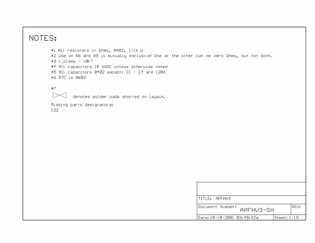
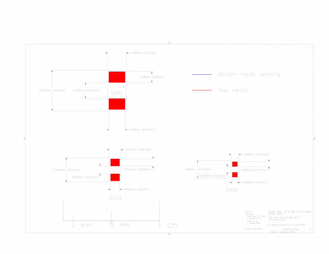
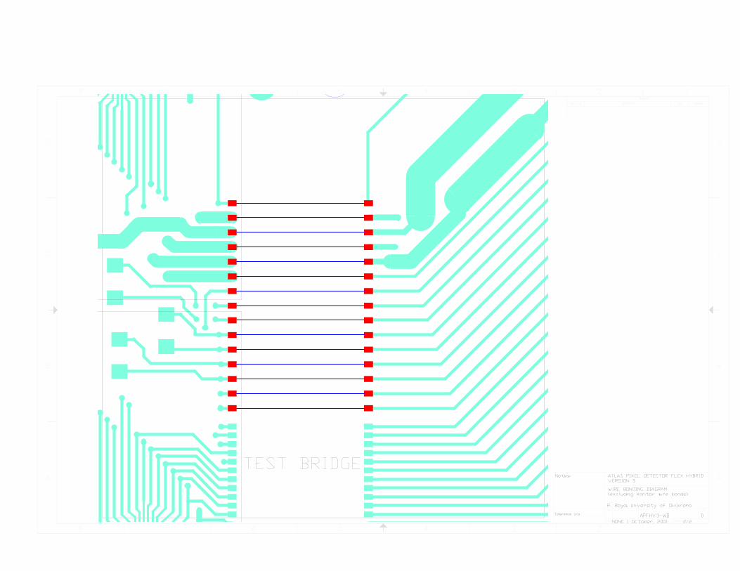
DESIGN FEATURESNote: Many (> 500) wire bond pads are on a 150 æm [5.9 mil] pitch. The traces from these padsare fanned out to a wider trace and space in a short distance. Most traces and spaces are 100 æm[3.9 mil].
Min. trace width 75 æm [2.9 mil]Min. trace space 75 æm [2.9 mil]Min. feature space

Via cover pad to trace* 100 æm [3.9 mil]Bond pad space 50 æm [2.0 mil]Bond pad size 100 æm x 300 æm [3.9 mil x 11.8 mil]Cover pad size* 200 æm diameter [7.9 mil]Via hole size* 25.4 æm [1 mil] minimum
* These parameters can be optimized for manufacturer's process
DESIGN FILE NOTESGerber files:
Device Gerber photoplotter with RS-274-X aperture generation
Parameter settings:OffsetX 0.000OffsetY 0.000
Plotfile Info: Coordinate Format 2.4 Coordinate Units Inch Data Mode Absolute Zero Suppression None End Of Block *
Drill file info: Tolerance Drill + 0.00 %Tolerance Drill - 0.00 %Rotate noMirror noOptimize yesAuto fit yesOffsetX 0.000OffsetY 0.000Format 2.4 (1/10000 in.)Zero suppression None
Drills used:Code Size Count Plated ThroughT01 0.050mm** 632 632T02 0.300mm 4 0T03 1.000mm 3 1 (see drawing)
** Via drill size can be optimized for fabrication process

FILE DEFINITIONS:File name Definitionapfhv3_fab.pdf This file (specifications, fabrication drawings, schematic, etc.)apfhv3_gerber.zip Zip file containing the following:
top.gbr Top metal layerbottom.gbr Bottom metal layerbottom_mask.gbr Bottom solder mask, negativetop_mask.gbr Top solder mask, negativecut.gbr Circuit outline (cutting guide)drill.xcl Excellon drill filerack.drl Drill tool list


V3 and v4.x Pigtail Connector Signals
Pin # Flex v3 Signal Name Flex v4.x Signal Name Pigtail Signal Name1 Vcal Vcal spare12 VDD_AMS VDD_AMS spare23 VDDA VDDA VDDA4 AGnd AGnd AGnd5 VDD VDD VDD6 DGnd DGnd DGnd7 STRIN DTO2N STRI/DTO2N8 STRIP DTO2P STRI/DTO2P9 RSIB RSIB RSIB10 DTON DTON DTON11 DTOP DTOP DTOP12 NTC_RET NTC_RET NTC_RET13 DCIN DCIN DCIN14 DCIP DCIP DCIP15 NTC NTC NTC16 XCKN XCKN XCKN17 XCKP XCKP XCKP
ATLAS PIXEL FLEX HYBRID MODULE PIGTAIL CONNECTOR
University of Olahoma Scale: n/aDwg.# Rev. A Units: n/aDrawn By: R. Boyd Date: 27 February, 2002

V3 and v4.x Test Connector Signals
Pad # Signal Name Pad # Signal Name3.x 4.x
1 Vcal 16 CCK2 VDD_AMS spare 2 17 DA3 DGnd 18 LD4 VDD 19 SYNCN5 AGnd 20 SYNCP6 VDDA 21 XCKN7 RSIB 22 XCKP8 DTOP 23 LV1N9 DTON 24 LV1P
10 STRIP DTO2P 25 STRN11 STRIN DTO2N 26 STRP12 DCIN 27 VDDA13 DCIP 28 VDD14 CKN 29 DGnd15 CKP 30 AGnd
ATLAS PIXEL FLEX HYBRID MODULE TEST CONNECTOR
University of Olahoma Scale: n/aDwg.# Rev. A Units: n/aDrawn By: R. Boyd Date: 26 February, 2002