( v ) preliminary specifications ( ) final specifications ... · pdf file( v ) preliminary...
TRANSCRIPT

1 of 30
AU OPTRONICS CORPORATION
Product Specification
B140RTN03.1 Document Version 0.3
( V ) Preliminary Specifications ( ) Final Specifications
Module 14.0” (13.98”) HD+ 16:9 Color TFT-LCD with LED Backlight design
Model Name B140RTN03.1 (H/W:0A)
Note ( ) LED Backlight with driving circuit design
Customer Date
HP /2012
Checked & Approved by
Date
Note: This Specification is subject to change without notice.
Approved by Date
Jonken Fan 09/04/2012
Prepared by Date
Queena Lee 09/04/2012
NBBU Marketing Division AU Optronics corporation
www.yslcd.com.tw
2 of 30
AU OPTRONICS CORPORATION
Product Specification
B140RTN03.1 Document Version 0.3
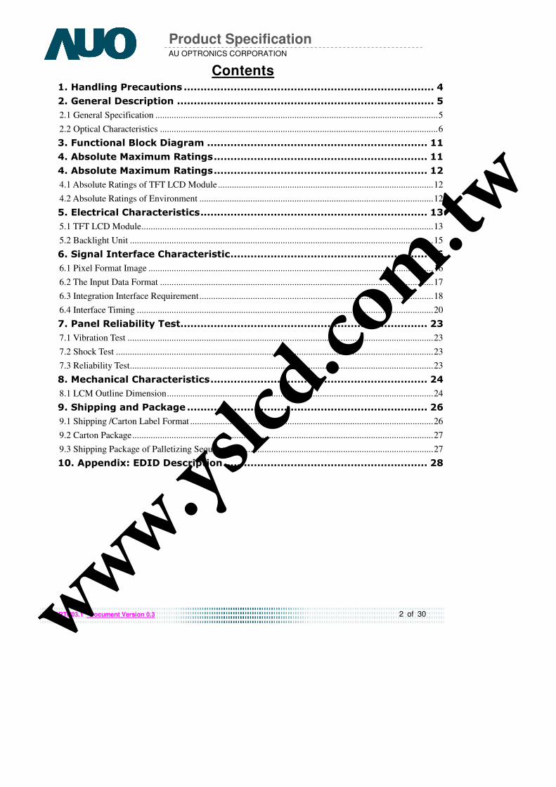
Contents 1. Handling Precautions ........................................................................... 4
2. General Description ............................................................................. 5
2.1 General Specification ..........................................................................................................................5
2.2 Optical Characteristics ........................................................................................................................6
3. Functional Block Diagram .................................................................. 11
4. Absolute Maximum Ratings................................................................ 11
4. Absolute Maximum Ratings................................................................ 12
4.1 Absolute Ratings of TFT LCD Module .............................................................................................12
4.2 Absolute Ratings of Environment .....................................................................................................12
5. Electrical Characteristics.................................................................... 13
5.1 TFT LCD Module..............................................................................................................................13
5.2 Backlight Unit ...................................................................................................................................15
6. Signal Interface Characteristic........................................................... 16
6.1 Pixel Format Image ...........................................................................................................................16
6.2 The Input Data Format ......................................................................................................................17
6.3 Integration Interface Requirement.....................................................................................................18
6.4 Interface Timing ................................................................................................................................20
7. Panel Reliability Test.......................................................................... 23
7.1 Vibration Test ....................................................................................................................................23
7.2 Shock Test .........................................................................................................................................23
7.3 Reliability Test...................................................................................................................................23
8. Mechanical Characteristics................................................................. 24
8.1 LCM Outline Dimension...................................................................................................................24
9. Shipping and Package ........................................................................ 26
9.1 Shipping /Carton Label Format .........................................................................................................26
9.2 Carton Package..................................................................................................................................27
9.3 Shipping Package of Palletizing Sequence........................................................................................27
10. Appendix: EDID Description............................................................. 28
www.yslcd.com.tw
3 of 30
AU OPTRONICS CORPORATION
Product Specification
B140RTN03.1 Document Version 0.3
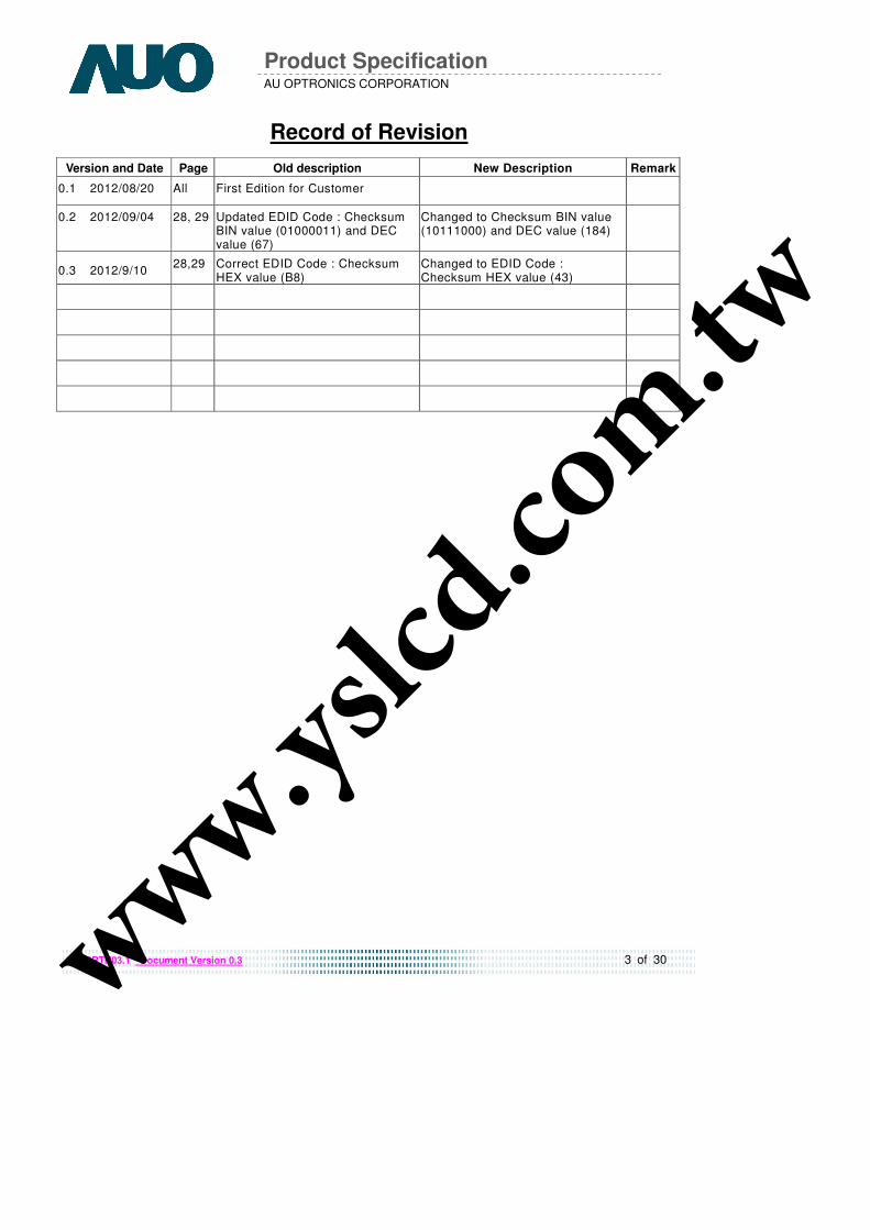
Record of Revision
Version and Date Page Old description New Description Remark
0.1 2012/08/20 All First Edition for Customer
0.2 2012/09/04 28, 29 Updated EDID Code : Checksum BIN value (01000011) and DEC value (67)
Changed to Checksum BIN value (10111000) and DEC value (184)
0.3 2012/9/10 28,29 Correct EDID Code : Checksum
HEX value (B8) Changed to EDID Code : Checksum HEX value (43)
www.yslcd.com.tw
4 of 30
AU OPTRONICS CORPORATION
Product Specification
B140RTN03.1 Document Version 0.3
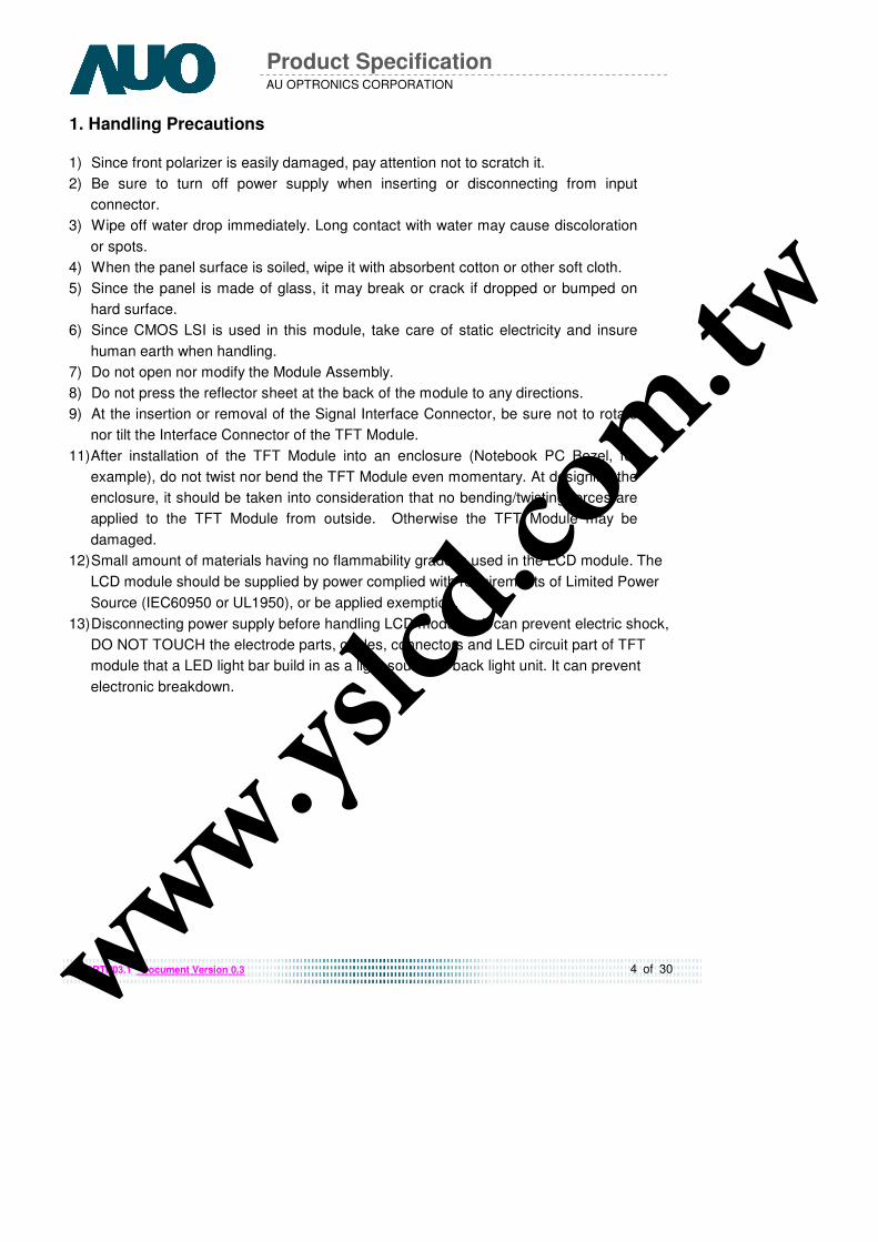
1. Handling Precautions 1) Since front polarizer is easily damaged, pay attention not to scratch it.
2) Be sure to turn off power supply when inserting or disconnecting from input
connector.
3) Wipe off water drop immediately. Long contact with water may cause discoloration
or spots.
4) When the panel surface is soiled, wipe it with absorbent cotton or other soft cloth.
5) Since the panel is made of glass, it may break or crack if dropped or bumped on
hard surface.
6) Since CMOS LSI is used in this module, take care of static electricity and insure
human earth when handling.
7) Do not open nor modify the Module Assembly.
8) Do not press the reflector sheet at the back of the module to any directions.
9) At the insertion or removal of the Signal Interface Connector, be sure not to rotate
nor tilt the Interface Connector of the TFT Module.
11) After installation of the TFT Module into an enclosure (Notebook PC Bezel, for
example), do not twist nor bend the TFT Module even momentary. At designing the
enclosure, it should be taken into consideration that no bending/twisting forces are
applied to the TFT Module from outside. Otherwise the TFT Module may be
damaged.
12) Small amount of materials having no flammability grade is used in the LCD module. The
LCD module should be supplied by power complied with requirements of Limited Power
Source (IEC60950 or UL1950), or be applied exemption.
13) Disconnecting power supply before handling LCD modules, it can prevent electric shock,
DO NOT TOUCH the electrode parts, cables, connectors and LED circuit part of TFT
module that a LED light bar build in as a light source of back light unit. It can prevent
electronic breakdown.
www.yslcd.com.tw

5 of 30
AU OPTRONICS CORPORATION
Product Specification
B140RTN03.1 Document Version 0.3
2. General Description
B140RTN03.1 is a Color Active Matrix Liquid Crystal Display composed of a TFT LCD panel,
a driver circuit, and LED backlight system. The screen format is intended to support the 16:9
HD, 1600(H) x900(V) screen and 262k colors (RGB 6-bits data driver) with LED backlight
driving circuit. All input signals are LVDS interface compatible.
B140RTN03.1 is designed for a display unit of notebook style personal computer and industrial machine.
2.1 General Specification
The following items are characteristics summary on the table at 25 ℃ condition:
Items Unit Specifications
Screen Diagonal [mm] 355.22
Active Area [mm] 309.60 X 174.15
Pixels H x V 1600x3(RGB) x 900
Pixel Pitch [mm] 0.1935X 0.1935
Pixel Format R.G.B. Vertical Stripe
Display Mode Normally White
White Luminance (Note: ILED is LED current)
[cd/m2]
250 typ. (5 points average) 212 min
Luminance Uniformity 1.25 max. (5 points)
Contrast Ratio 400 (typ)
Response Time [ms] 8 typ / 16 Max
Nominal Input Voltage VDD [Volt] +3.3 typ.
Power Consumption [Watt] 3.9 max. (Include Logic and Blu power)
Weight [Grams] 270 max.
Min. Typ. Max.
Length 319.9 320.4 320.9
Width 204.6 205.1 205.6
Physical Size Include bracket
[mm]
Thickness 3.0
Electrical Interface 2 channel LVDS
Glass Thickness [mm] 0.4
Surface Treatment Anti-Glare, Hardness 3H
Support Color 262K colors ( RGB 6-bit )
www.yslcd.com.tw
6 of 30
AU OPTRONICS CORPORATION
Product Specification
B140RTN03.1 Document Version 0.3
Temperature Range Operating Storage (Non-Operating)
[oC]
[oC]
0 to +50 -20 to +60
RoHS Compliance RoHS Compliance
2.2 Optical Characteristics
The optical characteristics are measured under stable conditions at 25℃ (Room
Temperature) :
Item Symbol Conditions Min. Typ. Max. Unit Note
White Luminance ILED=22mA
5 points average
212 250 - cd/m
2 1, 4, 5.
θR θL
Horizontal (Right) CR = 10 (Left)
40 40
45 45
-
- degree
Viewing Angle ψH ψL
Vertical (Upper) CR = 10 (Lower)
10 30
15 35
-
-
4, 9
Luminance Uniformity δ5P 5 Points - - 1.25 1, 3, 4
Luminance Uniformity δ13P 13 Points - - 1.53 2, 3, 4
Contrast Ratio CR 300 400 - 4, 6
Cross talk % 4 4, 7
Resoponse time TRT Rising + Falling - 8 16 msec
Rx TBD Red
Ry TBD
Gx TBD Green
Gy TBD
Bx TBD Blue
By TBD
Wx 0.283 0.313 0.343
Color / Chromaticity Coodinates
White Wy 0.299 0.329 0.359
NTSC %
CIE 1931
45
- 4
www.yslcd.com.tw
7 of 30
AU OPTRONICS CORPORATION
Product Specification
B140RTN03.1 Document Version 0.3
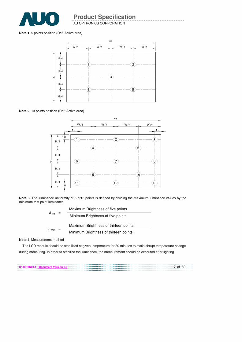
Note 1: 5 points position (Ref: Active area)
1 2
3
4 5
H /4
H /4
H /4
H /4
H
W
W /4 W /4 W /4 W /4
Note 2: 13 points position (Ref: Active area)
W /4
W
W /4
H
H /4
H /4
H /4
H /4
7
9 1 0
W /4
1
8
W /4
1 0
1 0
1 0
1 0
2 3
1 31 2
4 5
6
1 1
Note 3: The luminance uniformity of 5 or13 points is defined by dividing the maximum luminance values by the minimum test point luminance
Note 4: Measurement method
The LCD module should be stabilized at given temperature for 30 minutes to avoid abrupt temperature change
during measuring. In order to stabilize the luminance, the measurement should be executed after lighting
δW13 = Maximum Brightness of thirteen points Minimum Brightness of thirteen points
Maximum Brightness of five points δW5 = Minimum Brightness of five points
www.yslcd.com.tw
8 of 30
AU OPTRONICS CORPORATION
Product Specification
B140RTN03.1 Document Version 0.3
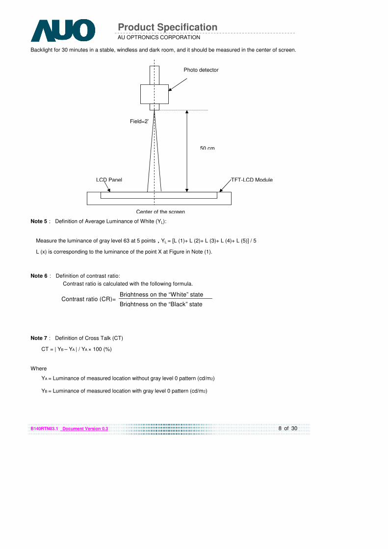
Backlight for 30 minutes in a stable, windless and dark room, and it should be measured in the center of screen.
Note 5: Definition of Average Luminance of White (YL):
Measure the luminance of gray level 63 at 5 points,YL = [L (1)+ L (2)+ L (3)+ L (4)+ L (5)] / 5
L (x) is corresponding to the luminance of the point X at Figure in Note (1).
Note 6: Definition of contrast ratio:
Contrast ratio is calculated with the following formula.
Note 7: Definition of Cross Talk (CT)
CT = | YB – YA | / YA × 100 (%)
Where
YA = Luminance of measured location without gray level 0 pattern (cd/m2)
YB = Luminance of measured location with gray level 0 pattern (cd/m2)
Center of the screen
TFT-LCD Module
50 cm
Photo detector
LCD Panel
Field=2°
Contrast ratio (CR)= Brightness on the “White” state
Brightness on the “Black” state
www.yslcd.com.tw
9 of 30
AU OPTRONICS CORPORATION
Product Specification
B140RTN03.1 Document Version 0.3
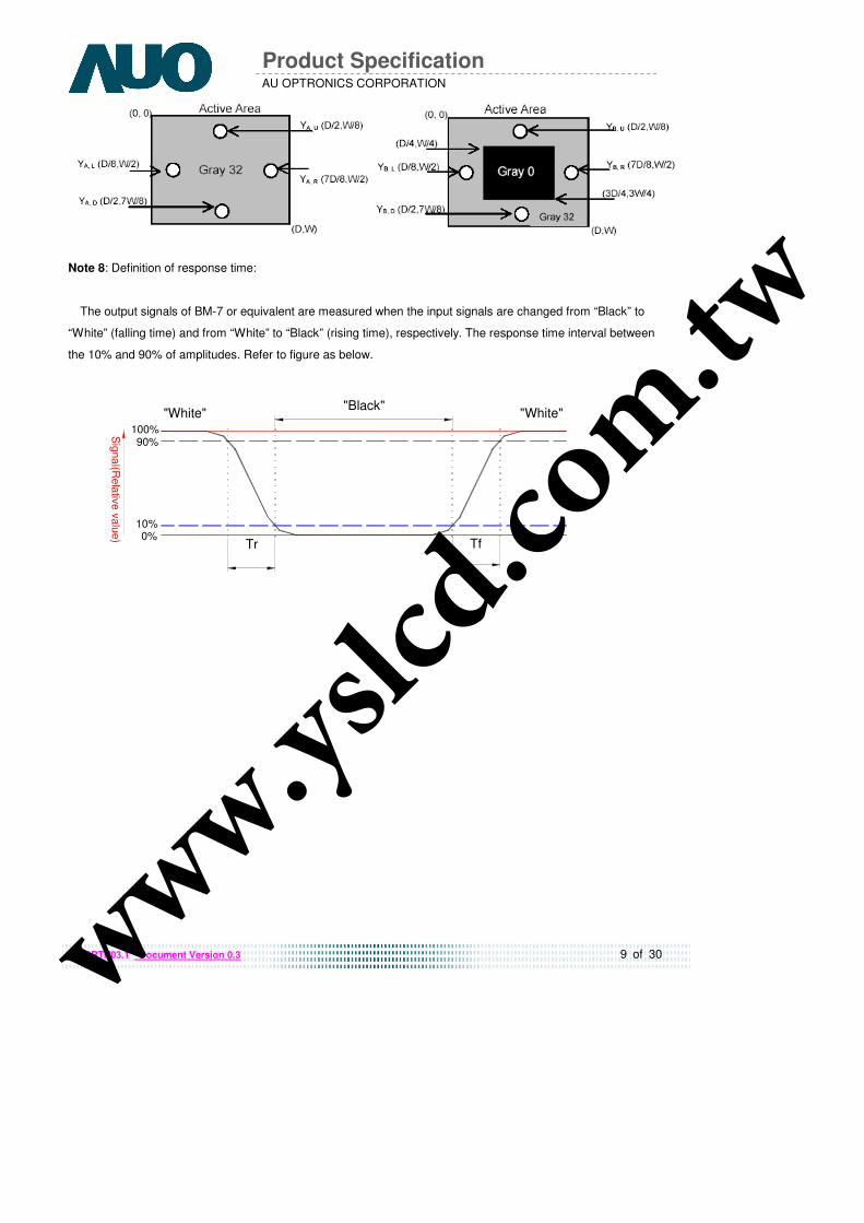
Note 8: Definition of response time:
The output signals of BM-7 or equivalent are measured when the input signals are changed from “Black” to
“White” (falling time) and from “White” to “Black” (rising time), respectively. The response time interval between
the 10% and 90% of amplitudes. Refer to figure as below.
Sig
na
l(Re
lativ
e v
alu
e)
"Black"
Tr Tf
"White""White"
0%10%
90%100%
www.yslcd.com.tw

10 of 30
AU OPTRONICS CORPORATION
Product Specification
B140RTN03.1 Document Version 0.3
Note 9. Definition of viewing angle
Viewing angle is the measurement of contrast ratio ≧ 10, at the screen center, over a 180° horizontal and
180° vertical range (off-normal viewing angles). The 180° viewing angle range is broken down as follows; 90°
(θ) horizontal left and right and 90° (Φ) vertical, high (up) and low (down). The measurement direction is
typically perpendicular to the display surface with the screen rotated about its center to develop the desired
measurement viewing angle.
www.yslcd.com.tw
11 of 30
AU OPTRONICS CORPORATION
Product Specification
B140RTN03.1 Document Version 0.3
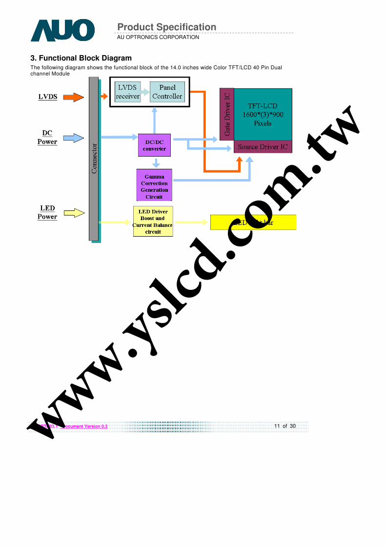
3. Functional Block Diagram The following diagram shows the functional block of the 14.0 inches wide Color TFT/LCD 40 Pin Dual channel Module
www.yslcd.com.tw
12 of 30
AU OPTRONICS CORPORATION
Product Specification
B140RTN03.1 Document Version 0.3
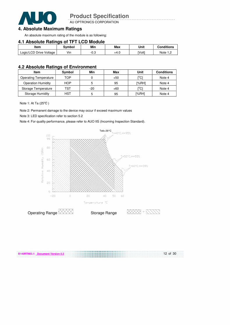
4. Absolute Maximum Ratings
An absolute maximum rating of the module is as following:
4.1 Absolute Ratings of TFT LCD Module Item Symbol Min Max Unit Conditions
Logic/LCD Drive Voltage Vin -0.3 +4.0 [Volt] Note 1,2
4.2 Absolute Ratings of Environment Item Symbol Min Max Unit Conditions
Operating Temperature TOP 0 +50 [oC] Note 4
Operation Humidity HOP 5 95 [%RH] Note 4
Storage Temperature TST -20 +60 [oC] Note 4
Storage Humidity HST 5 95 [%RH] Note 4
Note 1: At Ta (25℃ )
Note 2: Permanent damage to the device may occur if exceed maximum values
Note 3: LED specification refer to section 5.2
Note 4: For quality performance, please refer to AUO IIS (Incoming Inspection Standard).
Twb=39°C
Operating Range Storage Range
www.yslcd.com.tw
13 of 30
AU OPTRONICS CORPORATION
Product Specification
B140RTN03.1 Document Version 0.3
5. Electrical Characteristics
5.1 TFT LCD Module
5.1.1 Power Specification
Input power specifications are as follows;
The power specification are measured under 25℃ and frame frenquency under 60Hz
Symble Parameter Min Typ Max Units Note
VDD Logic/LCD Drive Voltage
3.0 3.3 3.6 [Volt]
PDD VDD Power - 1.25 [Watt] Note 1 IDD IDD Current - 417 [mA] Note 1
IRush Inrush Current - - 2000 [mA] Note 2
VDDrp Allowable Logic/LCD Drive Ripple Voltage
-
100 [mV] p-p
Note 1 : Maximum Measurement Condition:Black Pattern at 3.3V driving voltage. (Pmax=V3.3 x Iblack)
Note 2:Measure Condition
90%
10%
Vin rising time
0V
3.3V
0.5ms
註解註解註解註解 [MY1]:
PDD (max) = VDD(typ) x
IDD(max)
www.yslcd.com.tw
14 of 30
AU OPTRONICS CORPORATION
Product Specification
B140RTN03.1 Document Version 0.3
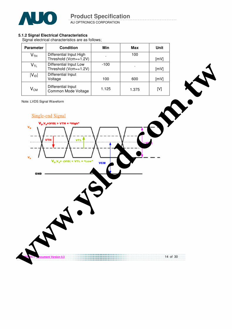
5.1.2 Signal Electrical Characteristics Signal electrical characteristics are as follows;
Parameter Condition Min Max Unit
VTH Differential Input High Threshold (Vcm=+1.2V)
- 100 [mV]
VTL Differential Input Low Threshold (Vcm=+1.2V)
-100 -
[mV]
|VID| Differential Input Voltage
100
600
[mV]
VCM Differential Input Common Mode Voltage
1.125 1.375 [V]
Note: LVDS Signal Waveform
www.yslcd.com.tw
15 of 30
AU OPTRONICS CORPORATION
Product Specification
B140RTN03.1 Document Version : 0.3
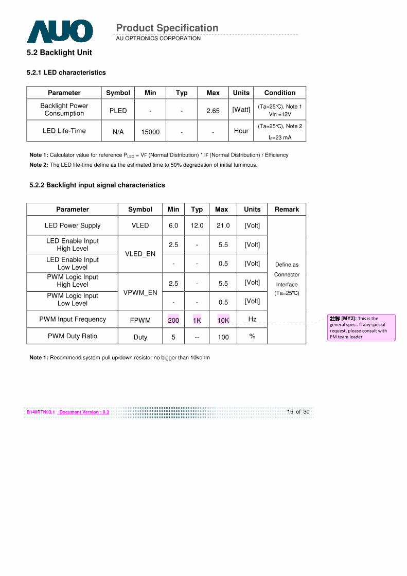
5.2 Backlight Unit
5.2.1 LED characteristics
Parameter Symbol Min Typ Max Units Condition
Backlight Power Consumption PLED - - 2.65 [Watt]
(Ta=25℃), Note 1
Vin =12V
LED Life-Time N/A 15000 - - Hour (Ta=25℃), Note 2
IF=23 mA
Note 1: Calculator value for reference PLED = VF (Normal Distribution) * IF (Normal Distribution) / Efficiency
Note 2: The LED life-time define as the estimated time to 50% degradation of initial luminous.
5.2.2 Backlight input signal characteristics
Parameter Symbol Min Typ Max Units Remark
LED Power Supply VLED 6.0 12.0 21.0 [Volt]
LED Enable Input High Level
2.5 - 5.5 [Volt]
LED Enable Input Low Level
VLED_EN
- - 0.5 [Volt]
PWM Logic Input High Level
2.5 - 5.5 [Volt]
PWM Logic Input Low Level
VPWM_EN
- - 0.5 [Volt]
PWM Input Frequency FPWM 200 1K 10K Hz
PWM Duty Ratio Duty 5 -- 100 %
Define as
Connector
Interface
(Ta=25℃)
Note 1: Recommend system pull up/down resistor no bigger than 10kohm
註解註解註解註解 [MY2]: This is the
general spec.. If any special
request, please consult with
PM team leader
www.yslcd.com.tw
16 of 30
AU OPTRONICS CORPORATION
Product Specification
B140RTN03.1 Document Version : 0.3
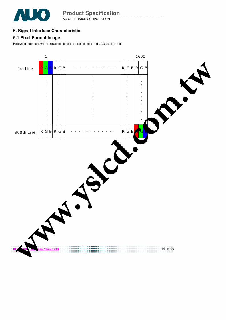
6. Signal Interface Characteristic
6.1 Pixel Format Image
Following figure shows the relationship of the input signals and LCD pixel format.
R G B R G B
R G B R G B
R G B R G B
R G B R G B
1 1600
1st Line
900th Line
www.yslcd.com.tw
17 of 30
AU OPTRONICS CORPORATION
Product Specification
B140RTN03.1 Document Version : 0.3
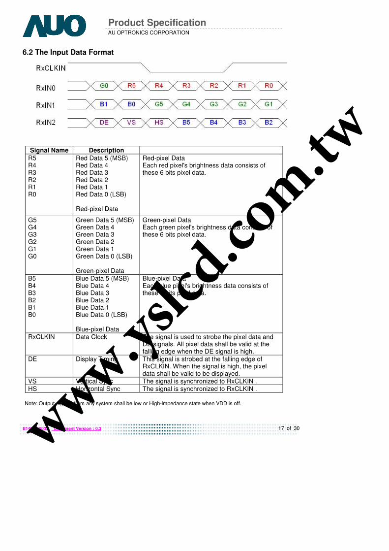
6.2 The Input Data Format
Signal Name Description
R5 R4 R3 R2 R1 R0
Red Data 5 (MSB) Red Data 4 Red Data 3 Red Data 2 Red Data 1 Red Data 0 (LSB) Red-pixel Data
Red-pixel Data Each red pixel's brightness data consists of these 6 bits pixel data.
G5 G4 G3 G2 G1 G0
Green Data 5 (MSB) Green Data 4 Green Data 3 Green Data 2 Green Data 1 Green Data 0 (LSB) Green-pixel Data
Green-pixel Data Each green pixel's brightness data consists of these 6 bits pixel data.
B5 B4 B3 B2 B1 B0
Blue Data 5 (MSB) Blue Data 4 Blue Data 3 Blue Data 2 Blue Data 1 Blue Data 0 (LSB) Blue-pixel Data
Blue-pixel Data Each blue pixel's brightness data consists of these 6 bits pixel data.
RxCLKIN Data Clock The signal is used to strobe the pixel data and DE signals. All pixel data shall be valid at the falling edge when the DE signal is high.
DE Display Timing This signal is strobed at the falling edge of RxCLKIN. When the signal is high, the pixel data shall be valid to be displayed.
VS Vertical Sync The signal is synchronized to RxCLKIN . HS Horizontal Sync The signal is synchronized to RxCLKIN .
Note: Output signals from any system shall be low or High-impedance state when VDD is off.
www.yslcd.com.tw
18 of 30
AU OPTRONICS CORPORATION
Product Specification
B140RTN03.1 Document Version : 0.3
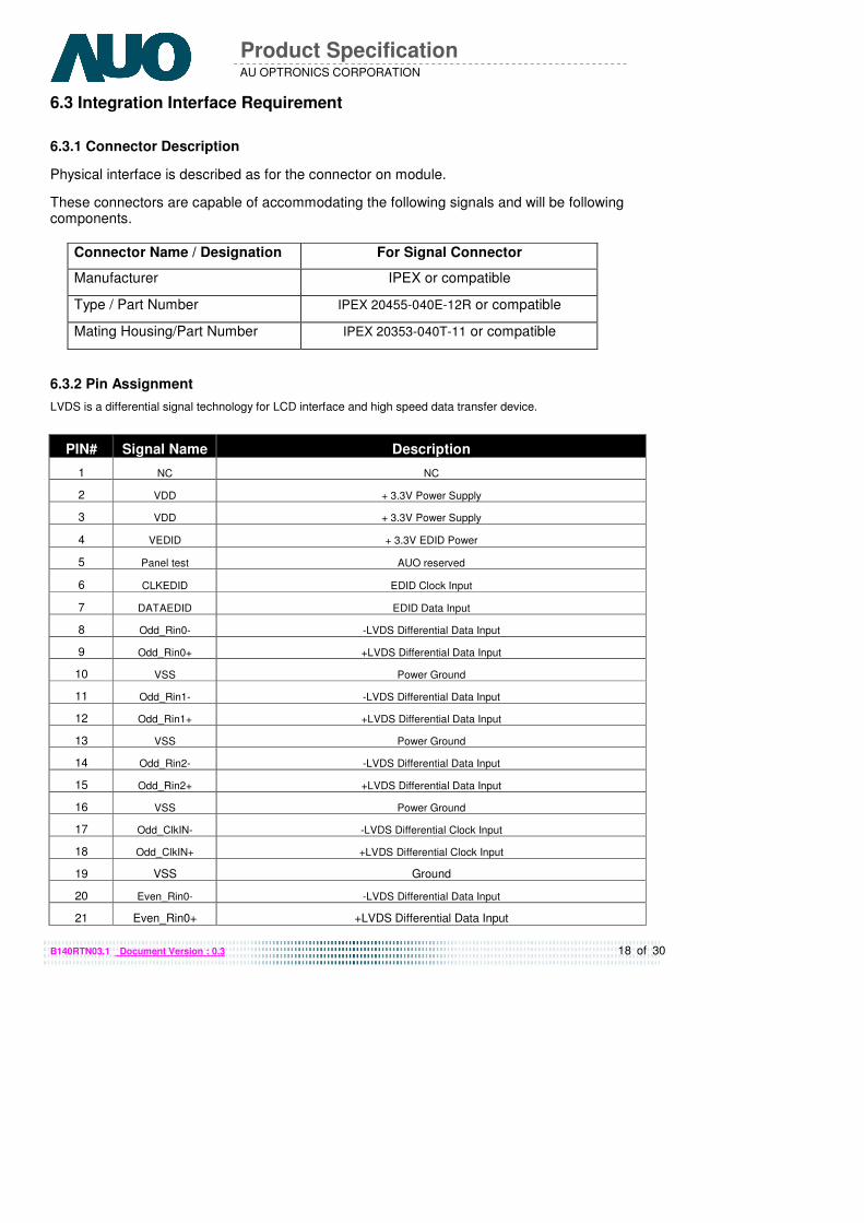
6.3 Integration Interface Requirement
6.3.1 Connector Description
Physical interface is described as for the connector on module.
These connectors are capable of accommodating the following signals and will be following components.
Connector Name / Designation For Signal Connector
Manufacturer IPEX or compatible
Type / Part Number IPEX 20455-040E-12R or compatible
Mating Housing/Part Number IPEX 20353-040T-11 or compatible
6.3.2 Pin Assignment
LVDS is a differential signal technology for LCD interface and high speed data transfer device.
PIN# Signal Name Description
1 NC NC
2 VDD + 3.3V Power Supply
3 VDD + 3.3V Power Supply
4 VEDID + 3.3V EDID Power
5 Panel test AUO reserved
6 CLKEDID EDID Clock Input
7 DATAEDID EDID Data Input
8 Odd_Rin0- -LVDS Differential Data Input
9 Odd_Rin0+ +LVDS Differential Data Input
10 VSS Power Ground
11 Odd_Rin1- -LVDS Differential Data Input
12 Odd_Rin1+ +LVDS Differential Data Input
13 VSS Power Ground
14 Odd_Rin2- -LVDS Differential Data Input
15 Odd_Rin2+ +LVDS Differential Data Input
16 VSS Power Ground
17 Odd_ClkIN- -LVDS Differential Clock Input
18 Odd_ClkIN+ +LVDS Differential Clock Input
19 VSS Ground
20 Even_Rin0- -LVDS Differential Data Input
21 Even_Rin0+ +LVDS Differential Data Input www.yslcd.com.tw

19 of 30
AU OPTRONICS CORPORATION
Product Specification
B140RTN03.1 Document Version : 0.3
22 VSS Power Ground
23 Even_Rin1- -LVDS Differential Data Input
24 Even_Rin1+ +LVDS Differential Data Input
25 VSS Power Ground
26 Even_Rin2- -LVDS Differential Data Input
27 Even_Rin2+ +LVDS Differential Data Input
28 VSS Power Ground
29 Even_ClkIN- -LVDS Differential Clock Input
30 Even_ClkIN+ +LVDS Differential Clock Input
31 VLED_GND LED_GND
32 VLED_GND LED_GND
33 VLED_GND LED_GND
34 NC NC
35 S-PWM Backlight_LED_PWM
36 LED_EN Backlight_LED_enable
37 NC NC
38 VLED LED_Positive (6~21)
39 VLED LED_Positive(6~21)
40 VLED LED_Positive(6~21)
Note1: Input signals shall be low or High-impedance state when VDD is off.
ww
w.yslcd.com.tw
20 of 30
AU OPTRONICS CORPORATION
Product Specification
B140RTN03.1 Document Version : 0.3
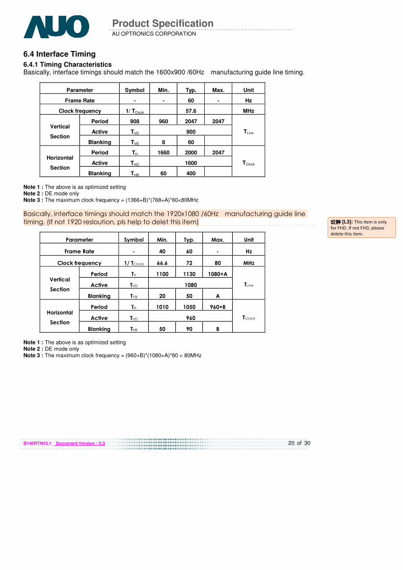
6.4 Interface Timing
6.4.1 Timing Characteristics Basically, interface timings should match the 1600x900 /60Hz manufacturing guide line timing.
Parameter Symbol Min. Typ. Max. Unit
Frame Rate - - 60 - Hz
Clock frequency 1/ TClock 57.6 MHz
Period 908 960 2047 2047
Active TVD 900 Vertical
Section Blanking TVB 8 60
TLine
Period TH 1660 2000 2047
Active THD 1600 Horizontal
Section Blanking THB 60 400
TClock
Note 1 : The above is as optimized setting Note 2 : DE mode only Note 3 : The maximum clock frequency = (1366+B)*(768+A)*60<80MHz
Basically, interface timings should match the 1920x1080 /60Hz manufacturing guide line
timing. (If not 1920 resloution, pls help to delet this item)
Parameter Symbol Min. Typ. Max. Unit
Frame Rate - 40 60 - Hz
Clock frequency 1/ TClock 66.6 72 80 MHz
Period TV 1100 1130 1080+A
Active TVD 1080 Vertical
Section
Blanking TVB 20 50 A
TLine
Period TH 1010 1050 960+B
Active THD 960 Horizontal
Section
Blanking THB 50 90 B
TClock
Note 1 : The above is as optimized setting Note 2 : DE mode only Note 3 : The maximum clock frequency = (960+B)*(1080+A)*60 < 80MHz
註解註解註解註解 [L3]: This item is only
for FHD. If not FHD, please
delete this item.
www.yslcd.com.tw
21 of 30
AU OPTRONICS CORPORATION
Product Specification
B140RTN03.1 Document Version : 0.3
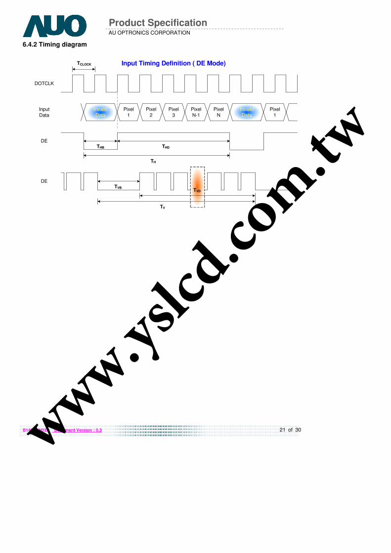
6.4.2 Timing diagram
DOTCLK
DE
TH
THB THD
DE
TV
TVB TVD
Input Timing Definition ( DE Mode) TCLOCK
Input
Data
Pixel
1
Pixel
2
Pixel
3
Pixel
N-1
Pixel
N
Invaild
Data
Invaild
Data
Pixel
1
www.yslcd.com.tw
22 of 30
AU OPTRONICS CORPORATION
Product Specification
B140RTN03.1 Document Version : 0.3
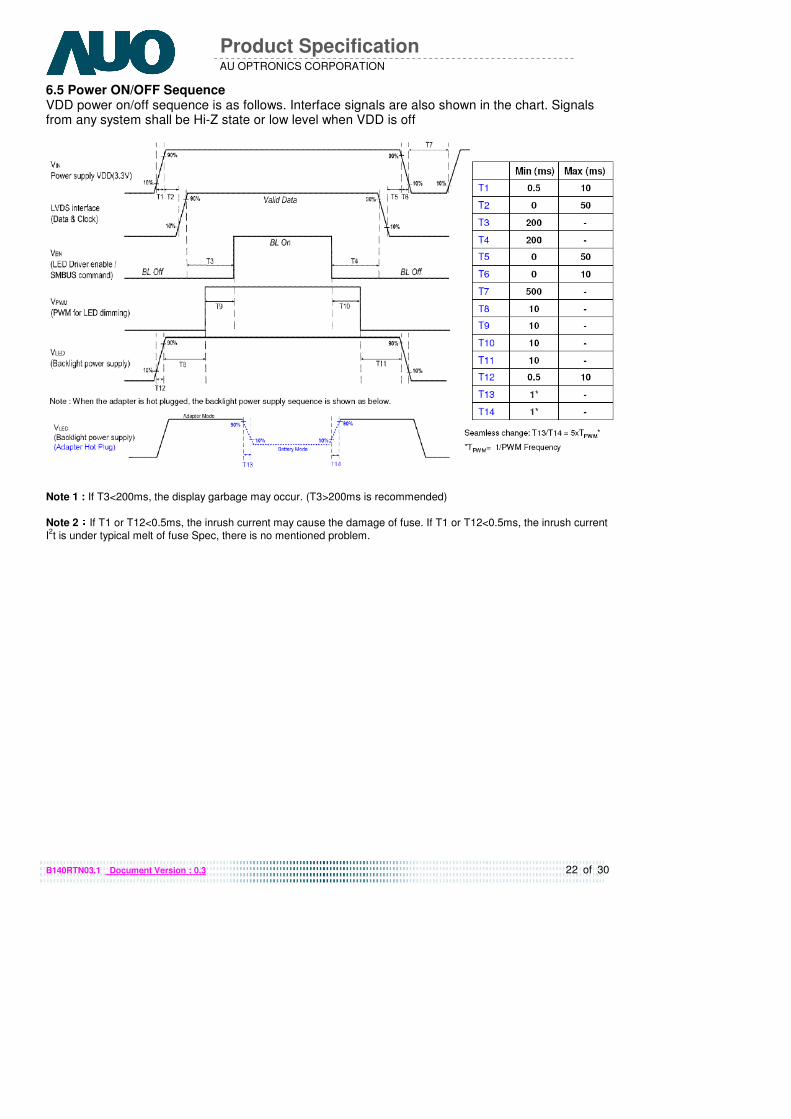
6.5 Power ON/OFF Sequence VDD power on/off sequence is as follows. Interface signals are also shown in the chart. Signals from any system shall be Hi-Z state or low level when VDD is off
Note 1 : If T3<200ms, the display garbage may occur. (T3>200ms is recommended)
Note 2::::If T1 or T12<0.5ms, the inrush current may cause the damage of fuse. If T1 or T12<0.5ms, the inrush current
I2t is under typical melt of fuse Spec, there is no mentioned problem.
www.yslcd.com.tw
23 of 30
AU OPTRONICS CORPORATION
Product Specification
B140RTN03.1 Document Version : 0.3
7. Panel Reliability Test
7.1 Vibration Test
Test Spec:
� Test method: Non-Operation
� Acceleration: 1.5 G
� Frequency: 10 - 500Hz Random
� Sweep: 30 Minutes each Axis (X, Y, Z)
7.2 Shock Test
Test Spec:
� Test method: Non-Operation
� Acceleration: 220 G , Half sine wave
� Active time: 2 ms
� Pulse: X,Y,Z .one time for each side
7.3 Reliability Test
Items Required Condition Note
Temperature
Humidity Bias Ta= 40℃℃℃℃, 90%RH, 300h
High Temperature
Operation Ta= 50℃℃℃℃, Dry, 300h
Low Temperature
Operation Ta= 0℃℃℃℃, 300h
High Temperature
Storage Ta= 60℃℃℃℃, 35%RH, 300h
Low Temperature
Storage Ta= -20℃℃℃℃, 50%RH, 250h
Thermal Shock
Test Ta=-20℃℃℃℃to 60℃℃℃℃, Duration at 30 min, 100 cycles
ESD Contact : ±8 KV
Air : ±15 KV
Note 1
Note1: According to EN 61000-4-2 , ESD class B: Some performance degradation allowed. No data lost
. Self-recoverable. No hardware failures.
Remark: MTBF (Excluding the LED): 30,000 hours with a confidence level 90%
www.yslcd.com.tw
24 of 30 B140RTN03.1 Document Version : 0.3
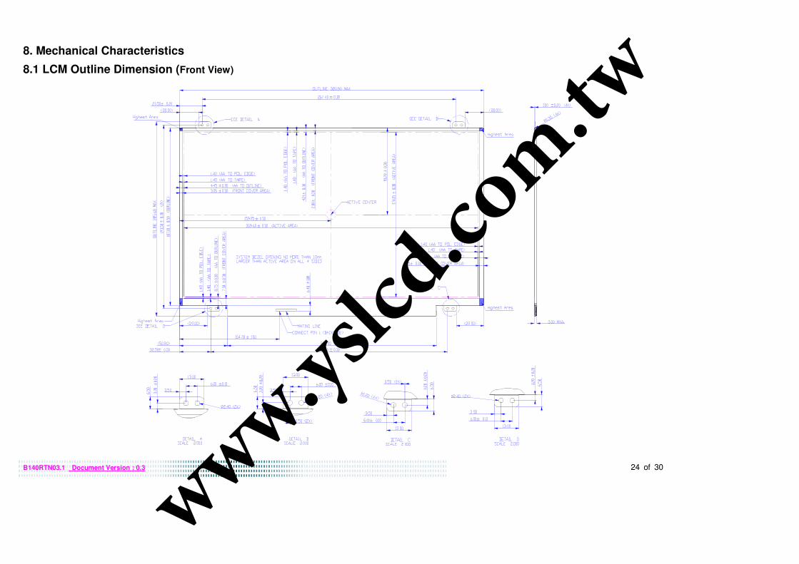
8. Mechanical Characteristics
8.1 LCM Outline Dimension (Front View)
www.
yslcd
.com.
tw
25 of 30 B140RTN03.1 Document Version : 0.3
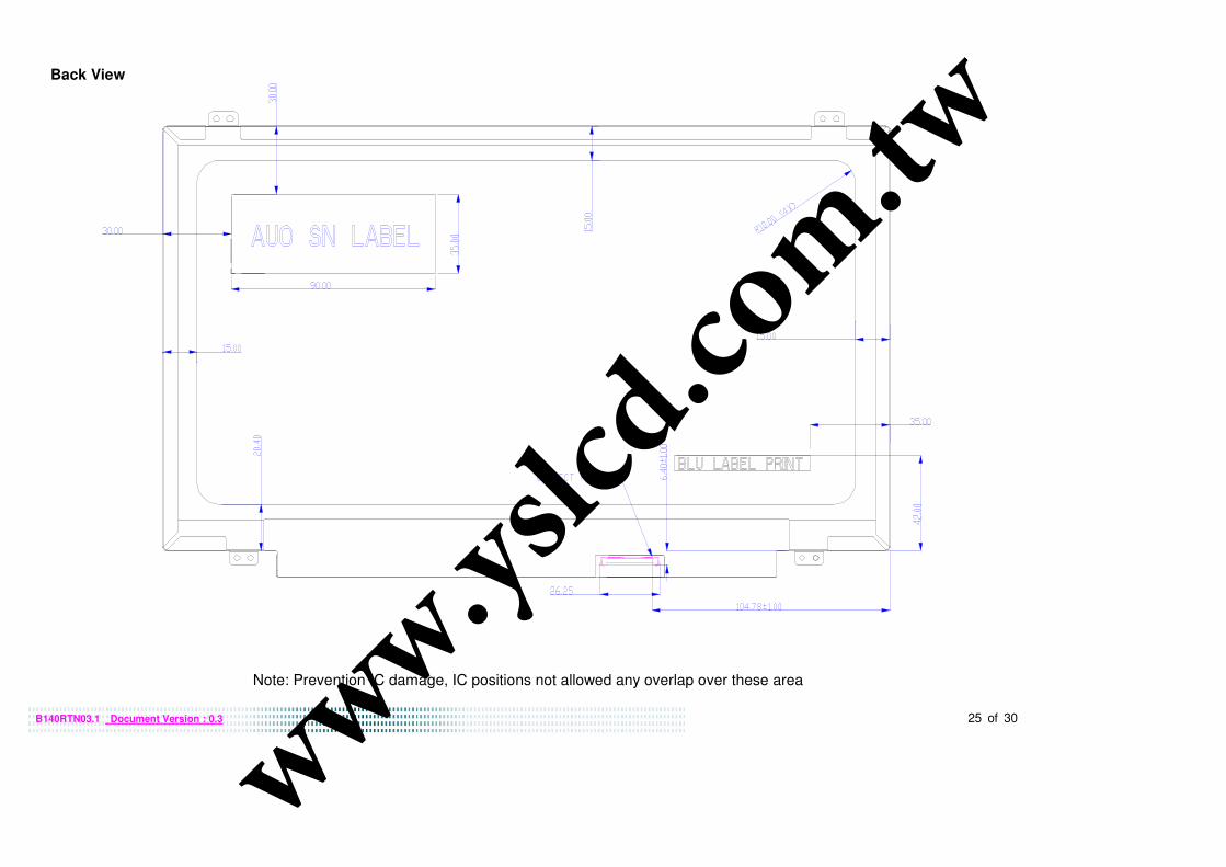
Back View
Note: Prevention IC damage, IC positions not allowed any overlap over these area
www.
yslcd
.com.
tw

26 of 30 B140RTN03.1 Document Version : 0.3
9. Shipping and Package
9.1 Shipping /Carton Label Format
www.yslcd.com.tw
27 of 30 B140RTN03.1 Document Version : 0.3
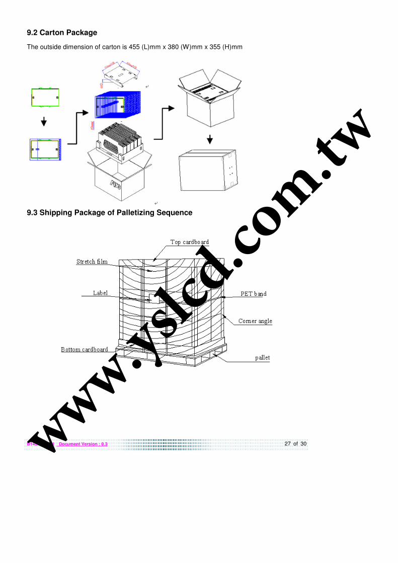
9.2 Carton Package
The outside dimension of carton is 455 (L)mm x 380 (W)mm x 355 (H)mm
9.3 Shipping Package of Palletizing Sequence
www.yslcd.com.tw
28 of 30 B140RTN03.1 Document Version : 0.3
10. Appendix: EDID Description
Address FUNCTION Value Value Value Note
HEX HEX BIN DEC
00 Header 00 00000000 0
01 FF 11111111 255
02 FF 11111111 255
03 FF 11111111 255
04 FF 11111111 255
05 FF 11111111 255
06 FF 11111111 255
07 00 00000000 0
08 EISA Manuf. Code LSB 06 00000110 6
09 Compressed ASCII AF 10101111 175
0A Product Code 3E 00111110 62
0B hex, LSB first 31 00110001 49
0C 32-bit ser # 00 00000000 0
0D 00 00000000 0
0E 00 00000000 0
0F 00 00000000 0
10 Week of manufacture 00 00000000 0
11 Year of manufacture 16 00010110 22
12 EDID Structure Ver. 01 00000001 1
13 EDID revision # 04 00000100 4
14 Video input def. (digital I/P, non-TMDS, CRGB) 90 10010000 144
15 Max H image size (rounded to cm) 1F 00011111 31
16 Max V image size (rounded to cm) 11 00010001 17
17 Display Gamma (=(gamma*100)-100) 78 01111000 120
18 Feature support (no DPMS, Active OFF, RGB, tmg Blk#1) 02 00000010 2
19 Red/green low bits (Lower 2:2:2:2 bits) A0 10100000 160
1A Blue/white low bits (Lower 2:2:2:2 bits) 95 10010101 149
1B Red x (Upper 8 bits) 99 10011001 153
1C Red y/ highER 8 bits 59 01011001 89
1D Green x 52 01010010 82
1E Green y 92 10010010 146
1F Blue x 26 00100110 38
20 Blue y 21 00100001 33
21 White x 50 01010000 80
22 White y 54 01010100 84
23 Established timing 1 00 00000000 0
24 Established timing 2 00 00000000 0 25 Established timing 3 00 00000000 0
26 Standard timing #1 01 00000001 1
27 01 00000001 1
28 Standard timing #2 01 00000001 1
29 01 00000001 1
2A Standard timing #3 01 00000001 1
2B 01 00000001 1
2C Standard timing #4 01 00000001 1 www.yslcd.com.tw
29 of 30 B140RTN03.1 Document Version : 0.3
2D 01 00000001 1
2E Standard timing #5 01 00000001 1
2F 01 00000001 1
30 Standard timing #6 01 00000001 1
31 01 00000001 1
32 Standard timing #7 01 00000001 1
33 01 00000001 1
34 Standard timing #8 01 00000001 1
35 01 00000001 1
36 Pixel Clock/10000 LSB FC 11111100 252
37 Pixel Clock/10000 USB 2B 00101011 43
38 Horz active Lower 8bits 40 01000000 64
39 Horz blanking Lower 8bits A0 10100000 160
3A HorzAct:HorzBlnk Upper 4:4 bits 61 01100001 97
3B Vertical Active Lower 8bits 84 10000100 132
3C Vertical Blanking Lower 8bits 1E 00011110 30
3D Vert Act : Vertical Blanking (upper 4:4 bit) 30 00110000 48
3E HorzSync. Offset 40 01000000 64
3F HorzSync.Width 2A 00101010 42
40 VertSync.Offset : VertSync.Width 33 00110011 51
41 Horz&Vert Sync Offset/Width Upper 2bits 00 00000000 0
42 Horizontal Image Size Lower 8bits 35 00110101 53
43 Vertical Image Size Lower 8bits AE 10101110 174
44 Horizontal & Vertical Image Size (upper 4:4 bits) 10 00010000 16
45 Horizontal Border (zero for internal LCD) 00 00000000 0
46 Vertical Border (zero for internal LCD) 00 00000000 0
47 Signal (non-intr, norm, no stero, sep sync, neg pol) 18 00011000 24
48 Pixel Clock/10,000 (LSB) 53 01010011 83
49 Pixel Clock/10,000 (MSB) 1D 00011101 29 40Hz frame rate
4A Horizontal Addressable Pixels, lower 8 bits 40 01000000 64
4B Horizontal Blanking Pixels, lower 8 bits A0 10100000 160
4C H Pixels, upper nibble : H Blanking, upper nibble 61 01100001 97
4D Vertical Addressable Lines, lower 8 bits 84 10000100 132
4E Vertical Blanking Lines, lower 8 bits 1E 00011110 30
4F V lines, upper nibble : V blanking, upper nibble 30 00110000 48
50 Horizontal Front Porch, lower 8 bits 40 01000000 64
51 Horizontal Sync Pulse, lower 8 bits 2A 00101010 42
52 V Front Porch, lower nibble : V Sync Pulse, lower nibble 33 00110011 51
53 VFP, 2 bits: VSP 2 bits: HFP 2 bits: HFP 2 bits 00 00000000 0
54 Horizontal Image Size in mm, lower 8 bits 35 00110101 53
55 Vertical Image Size in mm, lower 8 bits AE 10101110 174
56 H Image Size, upper nibble : V Image Size, upper nibble 10 00010000 16
57 Horizontal Border 00 00000000 0
58 Vertical Border 00 00000000 0
59 Bit Encode Sync Information 18 00011000 24
5A DC 00 00000000 0
5B HTOTAL 00 00000000 0
5C HA 00 00000000 0
nVDPS Reserved 00
www.yslcd.com.tw
30 of 30 B140RTN03.1 Document Version : 0.3
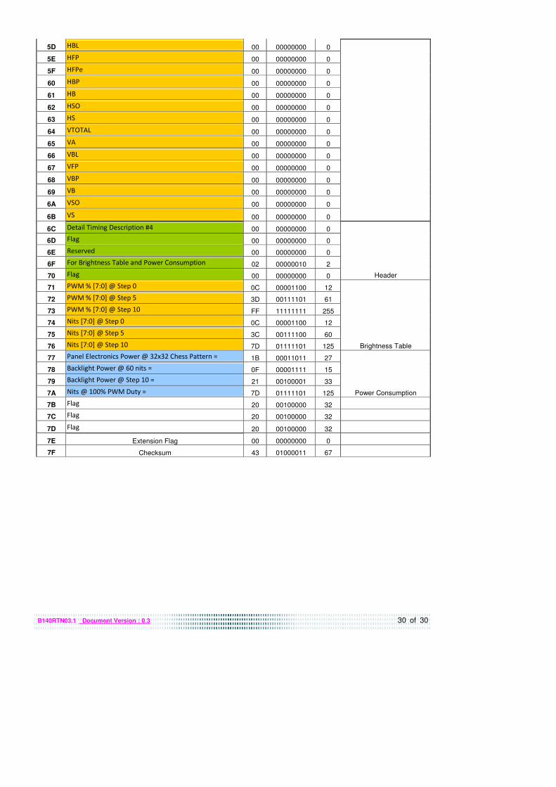
5D HBL 00 00000000 0
5E HFP 00 00000000 0
5F HFPe 00 00000000 0
60 HBP 00 00000000 0
61 HB 00 00000000 0
62 HSO 00 00000000 0
63 HS 00 00000000 0
64 VTOTAL 00 00000000 0
65 VA 00 00000000 0
66 VBL 00 00000000 0
67 VFP 00 00000000 0
68 VBP 00 00000000 0
69 VB 00 00000000 0
6A VSO 00 00000000 0
6B VS 00 00000000 0
6C Detail Timing Description #4 00 00000000 0
6D Flag 00 00000000 0
6E Reserved 00 00000000 0
6F For Brightness Table and Power Consumption 02 00000010 2
70 Flag 00 00000000 0 Header
71 PWM % [7:0] @ Step 0 0C 00001100 12
72 PWM % [7:0] @ Step 5 3D 00111101 61
73 PWM % [7:0] @ Step 10 FF 11111111 255
74 Nits [7:0] @ Step 0 0C 00001100 12
75 Nits [7:0] @ Step 5 3C 00111100 60
76 Nits [7:0] @ Step 10 7D 01111101 125 Brightness Table
77 Panel Electronics Power @ 32x32 Chess Pattern = 1B 00011011 27
78 Backlight Power @ 60 nits = 0F 00001111 15
79 Backlight Power @ Step 10 = 21 00100001 33
7A Nits @ 100% PWM Duty = 7D 01111101 125 Power Consumption
7B Flag 20 00100000 32
7C Flag 20 00100000 32
7D Flag 20 00100000 32
7E Extension Flag 00 00000000 0
7F Checksum 43 01000011 67
www.yslcd.com.tw