spatial light patterning of full color quantum dot
TRANSCRIPT

FULL PAPER
1701335 (1 of 9) © 2018 WILEY-VCH Verlag GmbH & Co. KGaA, Weinheim
www.advopticalmat.de
Spatial Light Patterning of Full Color Quantum Dot Displays Enabled by Locally Controlled Surface Tailoring
Han-Lim Kang, Jingu Kang, Jong Kook Won, Su-Min Jung, Jaehyun Kim, Chan Hyuk Park, Byung-Kwon Ju,* Myung-Gil Kim,* and Sung Kyu Park*
DOI: 10.1002/adom.201701335
Especially, colloidal lead halide perovskite quantum dots have been recently proven to be an excellent luminescent materials with nearly ideal efficiency.[4] Furthermore, other important kind of materials such as non-toxic I–III–VI systems are also emerged as important classes of quantum dot emit-ters.[5,6] Owing to these unique features, QDs have been studied for their use in a variety of industrial and scientific applica-tions, including photodetectors, thin-film transistors (TFTs), photovoltaics, and light-emitting diodes (LEDs).[7–12] More recently, colloidal QDs that can be synthesized and processed using a simple solution process have received significant attention, particu-larly in large area and high performance optoelectronic applications. Among these, QD-based LED (QLED) displays have been developed. These devices offer advantages over conventional organic LED displays due to their wide tunable color range, high color purity, and environmental stability. In achieving full color large-area QLED displays, an efficient high-resolution pat-terning technology remains a critical chal-
lenge. Research during the last decade has provided significant progress on patterning issues by employing several innovative methods including imprinting,[13–15] photolithography,[16,17] and inkjet printing.[18,19] Among these diverse methods, inkjet and contact printing[20] can pattern high-density multicolor QD devices with moderate accuracy and efficiency. These promising approaches facilitated the development of high-resolution QD-related electronic devices. However, their limited uniformity over the deposited area combined with the difficulty of performing large-area fabrication has limited the development of efficient manufacturing processes. Although previous photolithography-related approaches[16,17] have partially resolved the scaling and uniformity issues, they still require highly complicated device architectures and harsh fabrication processes that use organic solvents that may be detrimental to QD performance. Moreover, some repeated patterning technologies that employ additional relief processes[17] may not be compatible with efficient semi-conductor manufacturing processes. Therefore, the develop-ment of new materials, devices, and fabrication technologies for efficient high-resolution and large-area patterning of QD devices is required in order to achieve the widespread adoption of QD-related applications.
Quantum dot (QD) light-emitting diodes have been intensively investigated as a future display technology owing to their outstanding optoelectronic prop-erties such as narrow spectral bandwidths and high quantum efficiencies. Significant efforts have been made to achieve full color QD light-emitting diodes (QLEDs) by applying various fine-patterning technologies to active QD layers. However, the reported patterning methods generally require high processing cost and complex facilities which have limited their wide adoption in industrial-scale display applications. In this study, a fine patterning method is presented by employing spatial light-assisted and locally controlled surface tailoring. The chemical functionality of an interfacial polyethyleneimine (PEI) layer between ZnO and the QD layers is locally controlled by spatial light patterning (SLP), which is simultaneously used as a charge transfer layer and an anchoring agent for the selected QD nanoparticles. The versatility of this approach is demonstrated by patterning crossed stripes and multicolor QLED devices on selectively patterned PEI layers with a maximum luminescence of 1950 cd m−2 and a current efficiency of 2.9 cd A−1. The SLP process described herein is a general approach for fabricating full color QLEDs with marginal toxicity. This process is compatible with the standard complementary metal-oxide semiconductor (CMOS) processing technology.
H.-L. Kang, C. H. Park, Prof. B.-K. JuSchool of Electrical and Electronics EngineeringKorea UniversitySeoul 136-713, South KoreaE-mail: [email protected]. Kang, S.-M. Jung, J. Kim, Prof. S. K. ParkSchool of Electrical and Electronic EngineeringChung-Ang UniversitySeoul 06974, South KoreaE-mail: [email protected]. K. Won, Prof. M.-G. KimDepartment of ChemistryChung-Ang UniversitySeoul 06974, South KoreaE-mail: [email protected]
Full Color QLEDs
1. Introduction
In recent years, many studies have investigated the applica-tions of quantum dots (QDs) that promise attractive electronic and optoelectronic properties such as a high quantum effi-ciency, narrow spectral bandwidth, and controllable bandgap.[1–3]
Adv. Optical Mater. 2018, 6, 1701335

www.advancedsciencenews.com
© 2018 WILEY-VCH Verlag GmbH & Co. KGaA, Weinheim1701335 (2 of 9)
www.advopticalmat.de
In this study, we demonstrate efficient and simple patterning technologies that employ locally controlled surface tailoring of constitutional functional layers via photochemical deactiva-tion routes. The process yields finely patterned and scaled QD devices. Spatial light patterning (SLP) of polyethyleneimine (PEI; branched, molecular weight ≈25 000), a strong intercon-necting polymer, was utilized for the efficient and fine pat-terning of a QD layer. The high density of the amine functional groups in PEI allows it to be employed as both a charge transfer and anchor material in this study.[21] Multiple noncovalent inter-actions between PEI and the inorganic surfaces, such as dipole–dipole interactions, amine coordination on to a metal, and hydrogen bonding, were used to link specific functional layers to various nanostructured materials.[22–25] Moreover, an interfacial PEI layer deposited between electrically inhomogeneous layers, such as high work function metal/n-type or oxide/n-type organic semiconductors significantly modified the work function of the indium tin oxide (ITO) electrodes. Moreover, ZnO nanoparticles combined with dipolar PEI facilitated charge transport across the electrical energy barrier. This suggests that the material is a stable agent for efficient charge transfer.[21] In this study, the photolytic decomposition of PEI upon irradiation with ultravi-olet (UV) light from an excimer lamp (172 nm, 65 mW cm−2) induced the chemical decomposition of PEI and its amine groups, resulting in the loss of its dual functionality. Spatially selective UV irradiation was applied to PEI with a periodically patterned quartz mask, enabling locally controlled surface tai-loring of PEI. More importantly, multiple patterning steps can be performed with our strategy. We successfully developed finely patterned large-area red (R), green (G), and blue (B) QD films, as well as their corresponding inverted full color QLED devices.
2. Result and Discussion
In order to verify the effectiveness of the SLP-processed red, green, and blue QD layers, inverted multicolor QD-LEDs were fabricated on a borosilicate glass substrate. Figure 1a illus-trates a schematic of the inverted multicolor QD-LEDs. ZnO
nanoparticles (thickness of 55 nm) were spun over patterned ITO cathode electrodes and used as an electron transfer layer (ETL). After forming the ZnO ETL, PEI was spun and selectively removed via SLP process with a chrome-patterned quartz mask. Subsequently, core/shell type R, G, and B CdSe/ZnS QD layers were synthesized on the stacked ITO/ZnO/PEI layers to fab-ricate light-emitting layers (EMLs). After this step, 4,4′,4″-tris-(carbazol-9-yl) triphenylamine (TcTa), molybdenum (VI) oxide (MoO3), and aluminum (Al) were deposited using thermal evap-oration, creating a hole transport layer (HTL), a hole injection layer (HIL), and an anode electrode layer, respectively. Figure 1b and Figure S1 (Supporting Information) schematically describe the step-by-step process for fabricating fine-patterned QD LED arrays on a glass substrate. This process includes QD patterning of various layers on prepatterned PEI sites. These sites were patterned by spatial UV radiation via a chrome-coated quartz mask and the molecular tailoring of the PEI layer. The specific molecular structure of PEI was easily terminated by irradiation with highly energetic light. Irradiation caused the PEI to lose its functionality and induced subsequent removal when sub-jected to a mild ethanol rinse. In contrast, the nonirradiated PEI area remained on the ZnO ETL layer, possibly due to min-imal changes in the molecular structure. This resulted in intact structures inside the desired area after ethanol rinsing. On the predefined PEI structure, core/shell type CdSe/ZnS QDs were spun over the entire area and annealed for 5 min at 65 °C. Annealing improved the bonds between the PEI and QD layers. Strong multiple noncovalent interactions between the PEI and QD surfaces enable the strong adhesion of the QD layers, which can endure the typical solvent cleaning processes. In contrast, the regions where PEI was photochemically decomposed and removed with ethanol retained a weak dispersive force between the ZnO and QD surfaces.[26] Therefore, the weakly bonded QD nanoparticles were easy to remove using a simple toluene rinse. This allowed the retention of the assembled QD layers on the prepatterned PEI layer. To create full color QD layers, repeated PEI coatings, UV irradiation with appropriate quartz masks (for R, G, and B pixels), and rinsing were performed. This process reproduced each QD layer with minimal damage.
Adv. Optical Mater. 2018, 6, 1701335
Figure 1. a) Schematic of RGB full color QLED device. b) Illustration of photolithography process for patterning of quantum dots.
www.advancedsciencenews.com
© 2018 WILEY-VCH Verlag GmbH & Co. KGaA, Weinheim1701335 (3 of 9)
www.advopticalmat.de
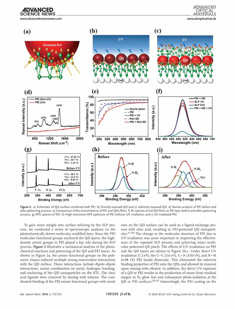
To gain more insight into surface tailoring by the SLP pro-cess, we conducted a series of spectroscopic analyses on the photochemically driven molecular modified layer. Since the PEI molecular functional groups anchored the QD layers, the high-density amine groups in PEI played a key role during the SLP process. Figure 2 illustrates a mechanical analysis of the photo-chemical reactions and patterning of the QD and PEI layers. As shown in Figure 2a, the amine functional groups on the poly-meric chains induced multiple strong noncovalent interactions with the QD surface. These interactions include dipole–dipole interactions, amine coordination on metal, hydrogen bonding, and anchoring of the QD nanoparticles on the ETL. The oleic acid ligands were removed by rinsing with toluene. The coor-dinated binding of the PEI amine functional groups with metal
ions on the QD surface can be used as a ligand exchange pro-cess with oleic acid, resulting in PEI-protected QD nanoparti-cles.[27,28] The change in the molecular structure of PEI due to UV irradiation was more important in improving the effective-ness of the repeated SLP process and achieving intact multi-color patterned QD pixels. The effects of UV irradiation on PEI and the QD layers are shown in Figure 2b,c. Under direct UV irradiation (7.2 eV), the CC (3.6 eV), CN (3.03 eV), and NH (4.08 eV) PEI bonds dissociate. This eliminated the inherent binding properties of PEI onto the QDs and allowed its removal upon rinsing with ethanol. In addition, the direct UV exposure of a QD or PEI results in the production of ozone from residual oxygen in N2 glove box and subsequent photo-oxidation at the QD or PEI surfaces.[26,29] Interestingly, the PEI coating on the
Adv. Optical Mater. 2018, 6, 1701335
Figure 2. a) Schematic of QD surface combined with PEI. b) Directly exposed QD and c) indirectly exposed QD. d) Raman analysis of PEI before and after patterning process. e) Comparison of the transmittance of PEI and QDs films. f) PL spectra of red QD films on PEI layer before and after patterning process. g) XPS spectra of PEI. h) High-resolution XPS spectrum of PEI without UV irradiation and i) UV-irradiated PEI.

www.advancedsciencenews.com
© 2018 WILEY-VCH Verlag GmbH & Co. KGaA, Weinheim1701335 (4 of 9)
www.advopticalmat.de
QD surface blocks the highly energetic UV irradiation and oxygen species adsorption on the QDs. This prevents photo-corrosion and unintentional QD adsorption. In addition, the quartz mask on the QDs suppresses residual oxygen penetra-tion and subsequent ozone generation, resulting in minimal degradation of the QD surfaces.
To study the chemical state of PEI, Raman spectroscopy was performed on UV-irradiated and nonirradiated PEI-coated glass substrates. As shown in Figure 2d, all of the vibrational, stretching, and bending peaks assigned to the CH2 (876 and 1299 nm), CN (1079 nm), and NH (1456 nm) bonds in PEI disappeared after UV irradiation. This clearly indicates the complete decomposition of the chemical structure of the PEI layer. On the other hand, the molecular structure of the PEI lying underneath the QD nanoparticles sustained minimal damage from the UV photons. The QD layer absorbed most of the UV energy and froze the excited molecular vibrations of PEI. Note that the confined organic molecules within inor-ganic cages can exhibit improved stability compared to free molecules; this is known to occur in dye molecules confined within zeolite cages.[30] Figure 2e shows a comparison of the optical transmittance of bare, QD-coated, and QD/PEI-coated quartz glass in the UV and visible regions. The transmittances of bare quartz glass in the visible and UV regions were more than 91% and 89%, respectively, whereas the transmission of a PEI-coated quartz glass dramatically decreased at shorter wave-lengths. These observations provide clear evidence for UV light absorption by the PEI layer. After UV irradiation on PEI, the oxidized functional groups, such as CO, NOH, and NO increased UV absorption. The oxidized functional groups fur-ther protect the QD surfaces from photo-oxidation. As shown in Figure S2 (Supporting Information), the gradual increase in UV absorption between 200 and 400 nm with deep ultraviolet (DUV) irradiation again confirmed the oxidation of the func-tional groups. The molecular structure of PEI decomposed due to the UV irradiation during SLP. The transmittance dropped below 60%, thus reducing the quantity of the UV photons reaching the QD layer. In addition, UV light absorption by the QD layer decreased the UV transmittance of the QD films and QD/PEI-coated quartz glass in the short wavelength region. The slight transmittance difference between the QD and QD/PEI-coated structures is attributed to the QD density difference between the respective films. The strong interaction between the QD surface and PEI molecule allowed the formation of a high-density QD layer in the QD/PEI structure. The composite layer exhibited a higher UV–vis absorption than the QD-only layer. The synergetic reduction of DUV penetration through the top PEI and QD layers protects the bottom PEI layer from DUV irradiation and photo-oxidation. Consequently, tailoring the undamaged surface of the PEI layer underneath the QDs ena-bled repeated SLP, allowing the creation of nearly intact struc-tured multicolor QD pixels. Although its underlying mecha-nisms require further research, we believe that the analysis presented above outlines a method for sustaining the molecular characteristics of a DUV-exposed PEI layer. The photolumines-cence (PL) characteristics of QD films during the SLP process confirmed the robustness of the QD/PEI layer. To examine the degradation of device performance during the SLP process, we performed PL measurement with multiple DUV-treated QD
layers after repeated SLP process. As shown in Figure 2f, the multiple SLP processes may slightly damage on the QD layer, resulting in somewhat degradation of PL intensity; however, the QD surface without over coated PEI layer (protected top layer) exhibited significant reduction of PL intensity (green line) pos-sibly due to photo-oxidation of the QD surface.[29]
As shown in Figure 2e, the top PEI layer and quartz mask during the SLP process reduced DUV penetration (by less than 50%) as well as the residual oxygen penetration. This sup-pressed the photo-oxidation of the PEI layer. The top PEI layer also suppresses the oxygen binding and photo-oxidation of the QD surfaces. The intact PL spectrum of the QD layer during the SLP process confirmed its stable adhesion to the substrate and the immunity of its surface to oxidation.
During the SLP process, the PEI is prepared with several patterning processes such as UV-irradiation under ambient nitrogen and ethanol washing process under ambient air. As a result, the PEI layer appears to be exposed to trace amount of water and oxygen during UV irradiation as well as substan-tial amount of ethanol during washing process. Similar to the thermal decomposition of PEI accompanying with gradual depolymerization of PEI (ultimately into CH2CHNH2),[31] the high energetic UV-irradiation might induce depolymeriza-tion reaction. Moreover, the residual oxygen and water within ambient nitrogen during the UV-irradiation are most likely attributed to the oxidation and hydroxylation of PEI chain. These findings may support the idea that noticeable decom-position and removal of PEI may be originated from the SLP processes. In Figure 2g,h,i, the X-ray photoelectron spectros-copy (XPS) results show the chemical modification of PEI by DUV irradiation and photo-oxidation. Figure 2g compares the wide energy survey spectra of PEI before and after UV irradi-ation. In both the scans, the peaks observed at 286, 400, and 532 eV are attributed to C1s, N1s, and O1s, respectively. Prior to the DUV irradiation of PEI, strong carbon (67.8 at%) and nitrogen (30.7 at%) peaks, and a weak oxygen (1.2 at%) peak were observed. After irradiation, the decreased N1s (23.6 at%) and increased O1s (8.0 at%) peaks confirmed the oxidation and loss of the amine functional group of PEI. The detailed XPS scan on the N1s peak shows the degree of PEI degradation due to UV irradiation (Figure 2h,i). The presence of neutral amine groups in pristine PEI was indicated by the N1s peak around 399 eV (Figure 2h). The nitrogen peak has two features, one at 398.5 eV corresponding to the bridging amine groups (NH) and a second at 400 eV corresponding to the terminal amine groups (NH2). The intensity of the latter peak has been reported to be mostly dependent on the bonds between PEI and the substrate.[28] After UV irradiation, the XPS spectra of the PEI layers show similar N 1s peaks but with smaller shoulders at 397.9 and 400.5 eV. These observations coincided with height reductions in the NH and NH2 peaks (Figure 2i). The XPS results also confirmed the formation of a decomposed PEI layer through the appearance of the oxidized NO (400.5 eV) and crosslinked tertiary amine (NR3: 397.9 eV) peaks. The relative abundance and binding energies of elements associated with the NO and NR3 peaks of PEI are consistent with previous work, which also shows the oxidation and crosslinking of NH and NH2.[32,33] The N1s XPS patterns in Figure 2h,i show a substantial decrease in the QD surface binding amine
Adv. Optical Mater. 2018, 6, 1701335

www.advancedsciencenews.com
© 2018 WILEY-VCH Verlag GmbH & Co. KGaA, Weinheim1701335 (5 of 9)
www.advopticalmat.de
groups after DUV irradiation, which again confirms the chem-ical functionality change in PEI during the SLP process. The main reason for the rather large decrease of nitrogen peak in XPS (after UV) is possibly due to the oxidation of PEI during the SLP processes which include amount of residual oxygen and water species the process atmosphere. The XPS spectra in Figure 2g–i shows dramatically decrease of nitrogen peak from 30 to 23.6 at% after UV treatment. To facilitate the efficient and full removal of the PEI, the ethanol rinsing process was carried out. As shown in Figure S3 (Supporting Information), the rinsing process resulted in significant removal of PEI on Si substrate with low nitrogen content of 3.4 at% and high Si content of 38.7 at%.
In addition to photodegradation stability, the chemical sta-bilities of EML and ETL are also important. Unfortunately, the QD and ZnO layers could be easily damaged by rinsing with the solvents used in SLP. This damage resulted in a poor device performance. Through the optimization of the interfacial layer and rinsing conditions, the PL and atomic force microscopy (AFM) measurements in Figure 3 confirmed that the pat-terned QD film and ZnO layer were robust during the toluene and ethanol rinsing processes. Figure 3a and Figure S4 (Sup-porting Information) show the effects of toluene rinsing on the QD layer with respect to various bottom PEI layer conditions. Depending on PEI concentration, the PL intensity of the QDs shows a different tendency after rinsing with toluene, whereby a QD layer on a denser PEI film shows a higher peak intensity. This appears to be closely related to the formation of a more uniform QD layer. Since the functional amine groups in PEI can induce strong multiple noncovalent interactions on the QD surfaces, the PEI molecules can be packed more densely by QD nanoparticles over the predefined PEI layer, thereby enhancing the PL peak. This shows that the SLP process, including rinsing with toluene, causes minimal damage to the QD nano-particles that coat the PEI layer. Unfortunately, increasing the PEI concentration in order to minimize the loss of QDs after rinsing can degrade QLED performance since PEI will act as an insulating layer.[34] On the other hand, after rinsing with toluene, a low-concentration QD layer coated on the patterned PEI could not maintain a uniform layer, and thus could not provide a uniform QLED pixel. When PEI was applied to the QLED, the device characteristics varied depending on the PEI concentration (Figure S5, Supporting Information). The elec-troluminescence (EL) of the QLED was measured by varying
the PEI concentration, and the optimum QLED performance was obtained at 0.8 wt% PEI while minimizing the damage to the QD layer. Moreover, the energy levels of the ZnO and QD layers were aligned by the use of the PEI layer.[35] As a result, the QLED efficiency was improved by 0.5 cd A−1 by using a PEI layer. Figure 3b shows the AFM image of the ZnO layer during the SLP process. In order to form a repeatable PEI pattern by UV irradiation, the ethanol rinsing process must be repeated. Ethanol was used as a dispersive solvent for the ZnO nanoparti-cles and as a solvent for the photodegraded portions of the PEI film. The nanoparticles on a uniformly coated ZnO layer were removed by ethanol to reduce its thickness by 10 nm and sur-face roughness by 0.7 nm after two patterning iterations. The slight damage to the ZnO layer only had a small effect on the QLED performance. Thus, SLP is a stable process that can be applied to the ZnO layer.
Figure 4a shows the PL image of the patterned 6 mm × 6 mm R, G, and B QD pixels on a glass substrate upon excitation with 356 nm UV light. The white dotted lines indicate the patterned area of each colored QD layer. In employing SLP on practical devices, multicolored inverted QLEDs were implemented based on previously described fabrication techniques. Figure 4b illus-trates the EL image of full color QLED devices with 4 mm × 4 mm pixel areas. To ensure minimal damage from repeated SLP appli-cations, the EL images and PL spectra were analyzed. These results clearly reveal the correct peak wavelengths for R (625 nm), G (530 nm), and B (440 nm), thereby confirming the quantum confinement characteristics of the SLP-processed QD pixels (Figure 4c). Since SLP utilizes the difference in bond strengths between the QDs and the underlying layers, such as selective strong multiple noncovalent and weak dispersive interactions, the toluene rinsing process easily overcame the small binding energy to yield controllably patterned structures. Based on the PL and EL analyses of the patterned QLED devices, it was concluded that the entire SLP process was repeatable and reproducible and mini-mized damage to the prepatterned QD layers.
The reliable and robust pattern prepared from colloidal QD nanoparticles using precisely controlled surface tailoring is exceptionally reproducible, suggesting new fabrication pos-sibilities for the next-generation full color QLED displays. However, high-resolution patterning and large-area formation remain significant challenges. Therefore, the development of simple, benign techniques for high performance area-scalable patterning is needed for next-generation QD-based electronics.
Adv. Optical Mater. 2018, 6, 1701335
Figure 3. a) PL spectra of red QD films, before and after rinsing. b) Thickness and roughness of ZnO nanoparticles coated on ITO glass.

www.advancedsciencenews.com
© 2018 WILEY-VCH Verlag GmbH & Co. KGaA, Weinheim1701335 (6 of 9)
www.advopticalmat.de
In this study, the reduced patterning area of each QD layer was observed in the PL images as a continuous and rectangular region (20 µm × 80 µm) when excited by 356 nm UV radiation (Figure 4d). Previous experiments have shown that partial expo-sure to UV light, possibly due to leakage or scattering from gaps between the quartz mask and sample, can occur in the shadow region, inducing a slight decomposition of the prepatterned PEI structures.[36] For the further fine patterning of full color QD layers, the undesired UV scattering should be minimized. To this end, we emphasize that hard contact or phase shift[37] masking process can alleviate the light scattering issues by reducing the air gap between photomask and sample surface.
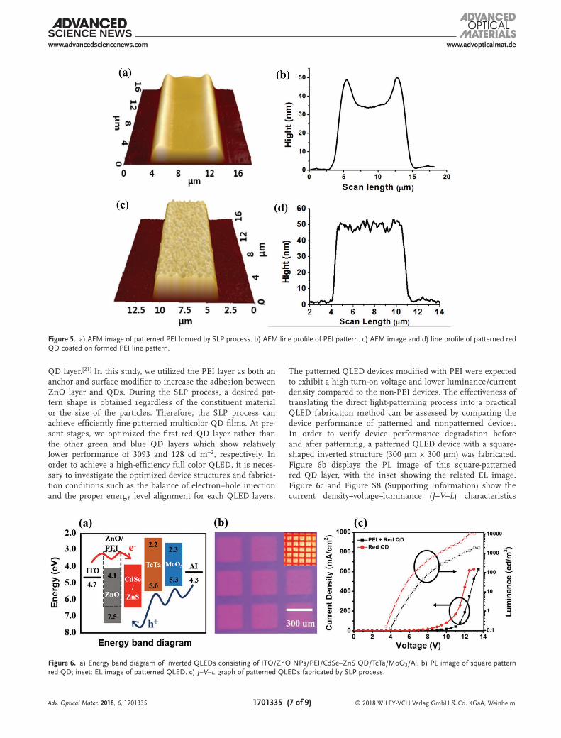
Here, we fabricated ultrafine structured rectangular (8 µm × 40 µm) and striped (width: 20 µm) patterns of multicolor QD layers for future on-chip device applications, as shown in Figure S6 (Supporting Information). To confirm the pre-cise dimensions and robust formation of the controllable fine structures, AFM was used after repeated application of the SLP process (Figure 5 and Figure S7, Supporting Information). Figure 5a,b show the fine-patterned PEI structures obtained on a glass substrate via the selective light-patterning and rinsing process. To clearly illustrate the formation of the alternative PEI structures, a 40 nm thick PEI layer was coated and pat-terned. Approximately 10 nm ridges at both the edges of the rectangular structure can be attributed to PEI crosslinking
upon UV irradiation, possibly due to undesirable UV leakage at the edge of the chrome mask. Figure 5c,d shows the AFM image and line profile of a SLP-processed QD layer. These results verify that minimal damage occurred on PEI after the QD patterning process, wherein a 10 nm QD layer was overlaid on the patterned PEI structure. As a result, the strongly bonded PEI layer is nearly intact after both the ethanol and toluene rinses, demonstrating the possibility of stable and uniformly scalable patterning for QD layers.
Since our approach can be easily implemented by a variety of fine-patterned QD-related applications with environmentally benign solution processes, we demonstrate its viability within a model for the scalable production of uniform multicolored QLED devices. In order to practically deliver fined-patterned QLED devices and translate the underlying mechanisms into device physics, we characterized the energy band levels of ZnO, the QDs, and the charge transporting/anchoring PEI layer.
Figure 6a provides a schematic illustration of the energy band diagram in an implemented QLED device. The sche-matic includes the energy level alignments of a layered struc-ture comprising ITO, ZnO, PEI, QD, TcTa, MoO3, and Al. Ultraviolet photoelectron spectroscopy revealed that PEI when incorporated with surface ZnO nanoparticles reduced the work function of the ZnO layer from 3.58 to 2.87 eV, thus facilitating electron injection and transport into the emissive CdSe/ZnS
Adv. Optical Mater. 2018, 6, 1701335
Figure 4. a) Patterned RGB QD films image of PL, excited by 365 nm UV radiation. b) Optical microscope image of simultaneous EL emission of a QLED on a single device at 9 V bias voltage. c) Full color PL spectra under photoactivation of patterned QD film. d) PL image of patterned RGB QDs coated on different substrates (, , and ) and on one substrate ().
www.advancedsciencenews.com
© 2018 WILEY-VCH Verlag GmbH & Co. KGaA, Weinheim1701335 (7 of 9)
www.advopticalmat.de
QD layer.[21] In this study, we utilized the PEI layer as both an anchor and surface modifier to increase the adhesion between ZnO layer and QDs. During the SLP process, a desired pat-tern shape is obtained regardless of the constituent material or the size of the particles. Therefore, the SLP process can achieve efficiently fine-patterned multicolor QD films. At pre-sent stages, we optimized the first red QD layer rather than the other green and blue QD layers which show relatively lower performance of 3093 and 128 cd m−2, respectively. In order to achieve a high-efficiency full color QLED, it is neces-sary to investigate the optimized device structures and fabrica-tion conditions such as the balance of electron–hole injection and the proper energy level alignment for each QLED layers.
The patterned QLED devices modified with PEI were expected to exhibit a high turn-on voltage and lower luminance/current density compared to the non-PEI devices. The effectiveness of translating the direct light-patterning process into a practical QLED fabrication method can be assessed by comparing the device performance of patterned and nonpatterned devices. In order to verify device performance degradation before and after patterning, a patterned QLED device with a square-shaped inverted structure (300 µm × 300 µm) was fabricated. Figure 6b displays the PL image of this square-patterned red QD layer, with the inset showing the related EL image. Figure 6c and Figure S8 (Supporting Information) show the current density–voltage–luminance (J–V–L) characteristics
Adv. Optical Mater. 2018, 6, 1701335
Figure 5. a) AFM image of patterned PEI formed by SLP process. b) AFM line profile of PEI pattern. c) AFM image and d) line profile of patterned red QD coated on formed PEI line pattern.
Figure 6. a) Energy band diagram of inverted QLEDs consisting of ITO/ZnO NPs/PEI/CdSe–ZnS QD/TcTa/MoO3/Al. b) PL image of square pattern red QD; inset: EL image of patterned QLED. c) J–V–L graph of patterned QLEDs fabricated by SLP process.

www.advancedsciencenews.com
© 2018 WILEY-VCH Verlag GmbH & Co. KGaA, Weinheim1701335 (8 of 9)
www.advopticalmat.de
of the two inverted red, green, and blue QLED devices. As expected, the patterned devices that include PEI as a sur-face modifier had lower performance than the nonpatterned devices. The devices also have a high turn-on voltage and low current density. However, the current became saturated at high voltages, and the device performance degraded. The PEI layer might limit the high-current flow and even limit the current efficiency value (2.9 cd A−1) at lower current densities compared to the nonpatterned devices, as shown in Figure S9 (Supporting Information).
In order to fabricate a high-efficiency QLED, it is necessary to study balance of electron–hole transport, proper energy levels alignment, and appropriate EML layer. Since the electrons are transported faster across ETL (ZnO) layer compared to the holes migrating through the HTL layer, excess electrons cause auger recombination and the electron–hole couple in layers other than the EML layer, which degraded the QLED perfor-mance.[38] Also, the improper energy band alignment between layers causes increase of turn-on voltage and decrease of effi-ciency. The PEI layer within patterned QLED can be used to these problems. The PEI layer can be used as electron blocking layer for ETL/HTL in QLED or work function control layer for EL devices.[21] The increased performance of QLED upon the addition of PEI can be achieved not only by employing a charge blocking barrier, but also by balancing the work functions between ZnO and the QDs. We believe that the performance of QLEDs based on a PEI layer can be further improved by opti-mizing charge injection (hole and electron) or carrier balance along with more appropriate material selection.
Although we have successfully fabricated full color QD dis-plays with fine patterning, the decreased luminescence after the SLP process may further be argued. On the basis of the dis-cussion and experimental findings, we argued that only a few monolayer of QDs can be loaded on top of the PEI layer. Since that only the QDs in direct contact with the PEI ligands may survive the post rinsing with toluene. This may be the main cause that the overall luminance is remarkably lower, due to the insufficient QD loading for emission.[39,40] In view of these experimental findings, multiple PEI–QD system and unique rinsing approaches which can form robust multilayered QDs with the SLP process are being investigated.
3. Conclusions
In summary, we demonstrated an efficient multilayer pat-terning process using QD nanoparticles for preparing fine-pat-terned full color QLED displays by employing locally controlled surface tailoring. The SLP process involving in-depth studies of the photochemically modified chemical structures of a PEI layer demonstrates a proof-of-concept as a practical procedure. The SLP technology can be applied as general nanomaterial patterning strategy, which is crucial for the industrial applica-tion of large-area electronic and optoelectronic devices. The SLP process could be further extended to the patterning of the other nanomaterials such as metal chalcogenide QDs, metal oxide QDs, carbon nanotubes, or silver nanowires. Further-more, this approach has the potential to set a milestone for the development of QD TFTs and QD-photosensor arrays by
the quasi-photolithographic methods of the amine functional groups on polymeric chains.[8,41]
Consequently, the results reported here imply that SLP can provide a general route to high-performance, extremely stable full color QLED devices with marginal toxicity and damage, offering compatibility with standard complementary metal-oxide semiconductor processing and large-scale device appli-cations. Although the advances reported in this study are noteworthy, a more systematic study is still needed to optimize the processes for high performance large scale QLED display fabrication.
4. Experimental SectionMaterial: The core/shell colloidal QDs for red and green QDs
were purchased from Eco-Flux, and blue QDs were purchased from NanoSquare. All QDs were covered with an oleic acid ligand. PEI (mean MW <20 000), dehydrated zinc acetate (≥98%), dimethyl sulfoxide (≥99.9%), tetramethylammonium hydroxide pentahydrate (≥97%), ethyl acetate (anhydrous, ≥99.8%), and ethanol (anhydrous, ≤0.0005% water) were purchased from Sigma-Aldrich.
Materials Synthesis: ZnO nanoparticles were synthesized using a solution–precipitation process as previously reported.[42] A solution of dehydrated zinc acetate in dimethyl sulfoxide (3 mmol) and 30 mL of a solution of tetramethylammonium hydroxide in ethanol (5.5 mmol) were mixed and stirred for 10 min in ambient air, then washed with ethyl acetate and dispersed in ethanol.
Device Fabrication: Inverted QLED devices were fabricated on ITO (thickness of 180 nm)-coated glass substrates. The windmill-patterned ITO glass was sonicated with acetone and isopropanol for 30 s and exposed to an oxygen plasma at 100 W for 30 s. ZnO nanoparticles (30 mg mL−1) were spun at 2000 rpm for 60 s and annealed at 90 °C for 30 min in a glove box, producing a mean particle thickness of 40 nm. PEI in ethanol (0.1 wt% in ethanol) was spin coated at 5000 rpm for 60 s under ambient air. Subsequently, UV irradiation (172 nm, 65 mW cm−2, L12530-01 MOD, Hamamatsu) was shone on the PEI layer through a chrome-coated quartz mask for 20 s, and then samples were washed with ethanol. QDs dispersed in toluene (5 mg mL−1) were spun over the patterned PEI layer at 4000 rpm for 50 s, and annealed in a glove box at 60 °C for 30 min. The QDs films were patterned by washing the QD film with toluene for 2 min and then sequentially annealed it in a glove box at 60 °C for 5 min. The identical process was repeated for each QD color. TcTa (50 nm), molybdenum (VI) oxide (MoO3, 10 nm), and aluminum (Al, anode, 150 nm) were thermally evaporated in a vacuum chamber to create a HTL, a HIL, and an anode electrode layer, respectively.
Measurement and Characterization: The J–V–L characteristics and EL spectra of the QLEDs were measured using a spectrophotometer (PR-670, Spectrascan) in a dark box at room temperature coupled to a voltage source (Model 237, Keithley) measurement unit. The morphological change of patterned QD films was characterized by noncontact mode AFM (NX-10, Park Systems). The patterned images of QDs were obtained by field emission scanning electron microscopy (Sigma, Carl Zeiss), and analyses were performed with an accelerating voltage of 10 kV. The PL of patterned QD films was obtained in the UV at 365 nm via an optical microscope (LV100N POL, Nikon), and the PL spectra of red, green, and blue (RGB) QD films were measured using a spectrometer (Ocean Optics, HR4000). The structural properties of the PEI layer were characterized by Raman spectroscopy (Bruker FRA 160/S, Burker). The chemical states of PEI were analyzed by XPS (K-Alpha+, ThermoFisher Science) using Al Kα radiation.
Supporting InformationSupporting Information is available from the Wiley Online Library or from the author.
Adv. Optical Mater. 2018, 6, 1701335

www.advancedsciencenews.com
© 2018 WILEY-VCH Verlag GmbH & Co. KGaA, Weinheim1701335 (9 of 9)
www.advopticalmat.de
AcknowledgementsThis research was supported by the Human Resources Development (No.20174030201810) of the Korea Institute of Energy Technology Evaluation and Planning (KETEP) grant funded by the Korea government Ministry of Trade, Industry and Energy, the Industrial Strategic Technology Development Program [10045145, Development of high performance (>70 cm−2 V−1 s−1) chalcogenide TFT backplane and cadmium-free highly efficient (>30 cd A−1) hybrid EL material/devices] funded by MOTIE/KEIT, and the National Research Foundation of Korea (NRF) funded by the Korea government (No. 2014M3A9B8023478).
Conflict of InterestThe authors declare no conflict of interest.
Keywordsfull color QLEDs, photochemical reaction, quantum dots, quantum-dot light-emitting diodes, spatial light patterning, surface tailoring
Received: December 7, 2017Revised: January 29, 2018
Published online: March 7, 2018
[1] A. P. Alivisatos, Science 1996, 271, 933.[2] D. V. Talapin, A. L. Rogach, A. Kornowski, M. Haase, H. Weller,
Nano Lett. 2001, 1, 207.[3] L. Qu, X. Peng, J. Am. Chem. Soc. 2002, 124. 2049.[4] F. Zhang, H. Zhong, C. Chen, X. G. Wu, X. Hu, H. Huang, J. Han,
B. Zou, Y. Dong, ACS Nano 2015, 9, 4533.[5] B. Chen, N. Pradhan, H. Zhong, J. Phys. Chem. Lett. 2018, 9, 435.[6] H. Zhong, Z. Bai, B. Zou, J. Phys. Chem. Lett. 2012, 3, 3167.[7] V. Sukhovatkin, S. Hinds, L. Brozozowski, E. H. Sargent, Science
2009, 324, 1542.[8] D. V. Talapin, C. B. Murray, Science 2005, 310, 86.[9] C.-H. M. chuang, P. R. Brown, V. Bulovic, M. G. Bawendi,
Nat. Mater. 2014, 13, 796.[10] V. L. Colvin, M. C. Schlamp, A. P. Alivisatos, Nature 1994, 370,
354.[11] Q. Sun, Y. A. Wang, L. S. Li, D. Wang, T. Zhu, J. Xu, C. Yang, Y. Li,
Nat. Photonics 2007, 1, 717.[12] B. S. Mashford, M. Stevenson, Z. Popovic, C. Hamilton, Z. Zhou,
C. Breen, J. Steckel, V. Bulovic, M. Bawendi, S. C. Sullivan, P. T. Kazlas, Nat. Photonics 2013, 7, 407.
[13] T. H. Kim, K. S. Cho, E. K. Lee, S. J. Lee, J. Chae, J. W. Kim, D. H. Kim, J. Y. Kwon, G. Amaratunga, S. Y. Lee, B. L. choi, Y. Kuk, J. M. Kim, K. Kim, Nat. Photonics 2011, 5, 176.
[14] B. H. Kim, S. J. Nam, N. R. Oh, S. Y. Cho, K. J. Yu, C. H. Lee, J. Zhang, K. Deshpande, P. Trefonas, J. H. Kim, J. Y. Lee, J. H. Shin, Y. J. Yu, J. B. Lim, S. M. Won, Y. K. Cho, N. H. Kim, K. J. Seo, H. N. Lee, T. I. Kim, M. S. Shim, J. A. Rogers, ACS Nano 2016, 10, 4920.
[15] M. K. Choi, J. W. Yang, K. H. Kang, D. C. Kim, C. S. Choi, C. E. Park, S. J. Kim, S. I. Chae, T.-H. Kim, J. H. Kim, T. H. Hyeon, D.-H. Kim, Nat. Commun. 2015, 6, 7149.
[16] J. J. Park, P. Prabhakaran, K. K. Jang, Y. G. Lee, J. H. Lee, K. H. Lee, J. H. Hur, J. M. Kim, N. C. Cho, Y. Son, D. Y. Yang, K. S. Lee, Nano Lett. 2010, 10, 2310.
[17] J. S. Park, J. Kyhm, H. H. Kim, S. Y. Jeong, J. H. Kang, S. E. Lee, K. T. Lee, K. S. Park, N. Barange, J. Y. Han, J. D. Song, W. K. Choi, Il. K. Han, Nano Lett. 2016, 16, 6946.
[18] V. Wood, M. J. panzer, J. Chen, M. S. Bradly, J. E. Halpert, M. G. Bawendi, V. Bulovic, Adv. Mater. 2009, 21, 2151.
[19] H. M. Haverinen, R. A. Myllylä, G. E. Jabbour, Appl. Phys. Lett. 2009, 94, 073108.
[20] L. A. Kim, P. O. Anikeeva, S. A. Coe-Sullivan, J. S. Steckel, M. G. Bawendi, V. Bulovic,Nano Lett. 2008, 8, 4513.
[21] H. H. Kim, S. Park, Y. Yi, D. I. Son, C. Park, D. K. Hwang, W. K. Choi, Sci. Rep. 2015, 5, 8968.
[22] Y. Zhou, C. F. Hernandez, J. Shim, J. Meyer, A. J. Giordano, H. L, P. Winget, T. Papadopoulos, H. Cheun, J. B. Kim, M. Fenoll, A. Dindar, W. Haske, E. Najafabadi, T. M. Khan, H. Sojoudi, S. Barlow, S. Graham, J. Luc Brédas, S. R. Marder, A. Kahn, B. Kippelen, Science 2012, 336, 327.
[23] O. Boussif, F. Lezoualc’h, M. A. Zanta, M. D. Mergny, D. Scherman, B. Demeneix, J. P. Behr, Proc. Natl. Acad. Sci. USA 1995, 92, 7297.
[24] T. Xia, M. Kovochich, M. Liong, H. Meng, S. Kabehie, S. George, J. I. Zink, A. E. Nel, ACS Nano 2009, 3, 3273.
[25] E. P. Dillon, C. A. Crouse, A. R. Barron, ACS Nano 2008, 2, 156.[26] H. Hu, Y. Ni, S. K. Mandal, V. Montana, B. Zhao, R. C. Haddon,
V. Parpura, J. Phys. Chem. B 2005, 109, 4285.[27] S. Sun, S. Anders, H. F. Hamann, J. U. Thiele, J. E. E. Baglin,
T. Thomson, E. E. Fullerton, C. B. Murray, B. D. Terris, J. Am. Chem. Soc. 2002, 124, 2884.
[28] T. Nann, Chem. Commun. 2005, 13, 1735.[29] S. C. Carrillo-Carrión, B. M. Simonet, M. Valcárcel, Chem. Commun.
2009, 5214.[30] M. L. Cano, F. L. Cozens, M. A. Esteves, F. marquez, H. Garcia,
J. Org. Chem. 1997, 62, 7121.[31] A. K. Burrell, T. M. Mcleskey, Q. X. Jia, Chem. Commun. 2008,
11, 1271.[32] J. R. Pels, F. Kapteijn, J. A. Moulijin, Q. Zhu, K. M. Thomas, Carbon
1995, 33, 1641.[33] R. Scatena, P. Bottoni, A. Pontoglio, B. Giardina, Curr. Med. Chem.
2010, 17, 61.[34] K. Ding, H. Chen, L. Fan, B. Wang, Z. Huang, S. Zhuang, B. Hu,
L. Wang, ACS Appl. Mater. Interfaces 2017, 9, 20231.[35] H. H. Kim, S. H. Park, Y. J. Y, D. I. Son, C. M. Park,
D. K. Hwang, W. K. Choi, Sci. Rep. 2015, 5, 8968.[36] J. S. Heo, T. H. Kim, S. G. Ban, D. S. Kim, J. H. Lee, J. S. Jur,
M.-G. Kim, Y. H. Kim, Y. T. Hong, S. K. Park, Adv. Mater. 2017, 29, 1701822.
[37] H. Miyajima, M. Mehregany, J. Microelectromech. Syst. 1995, 4, 220.[38] H. Y. Kim, Y. J. Park, J. W. Kim, C. J. Han, J. N. Lee, Y. H. Kim,
T. Greco, C. Ippen, A. Wedel, B. K. Ju, M. S. Oh, Adv. Funct. Mater. 2016, 26, 3454.
[39] W. K. Bae, J. H. Kwak, J. H. Lim, D. G. Lee, M. K. Nam, K. H. Char, C. H. Lee, S. H. Lee, Nano Lett. 2010, 10, 2368.
[40] M. Y. Gao, C. Lesser, S. Kirstein, H. Mojwald, A. L. Rogach, H. Weller, J. Appl. Phys. 2000, 87, 2297.
[41] J. H. Kim, J. K. Kim, S. H. Jo, J. G. Kang, J. W. Jo, M. W. Lee, J. H. Moon, L. Yang, M.-G. Kim, Y.-H. Kim, S. K. Park, Adv. Mater. 2016, 28, 3078.
[42] L. Qian, Y. Zheng, J. Xue, P. H. Holloway, Nat. Photonics 2011, 5, 543.
Adv. Optical Mater. 2018, 6, 1701335