sp4 witch hswa4-63dr+ - mini-circuits
TRANSCRIPT

SP4T RF Switch
Page 1 of 5
NotesA. Performance and quality attributes and conditions not expressly stated in this specification document are intended to be excluded and do not form a part of this specification document. B. Electrical specifications and performance data contained in this specification document are based on Mini-Circuit’s applicable established test performance criteria and measurement instructions. C. The parts covered by this specification document are subject to Mini-Circuits standard limited warranty and terms and conditions (collectively, “Standard Terms”); Purchasers of this part are entitled to the rights and benefits contained therein. For a full statement of the Standard Terms and the exclusive rights and remedies thereunder, please visit Mini-Circuits’ website at www.minicircuits.com/MCLStore/terms.jsp
Mini-Circuits®
www.minicircuits.com P.O. Box 350166, Brooklyn, NY 11235-0003 (718) 934-4500 [email protected]
HSWA4-63DR+
The Big Deal• High Isolation, 61 dB @ 0.9 GHz• Low insertion loss, 0.9 dB at 0.9 GHz• High IP3, +58 dBm• Fast switching, 255ns• Low current consumption, 110µA• Immune to latch-up
Product OverviewMini-Circuits’ HSWA4-63DR+ is a MMIC SP4T absorptive switch with an internal driver designed for wide-band operation from 30 MHz to 6 GHz, supporting many applications requiring high performance across a wide frequency range. This model provides excellent isolation, fast switching speed and high linearity in a tiny 4x4mm 24-Lead MCLP package. Produced using a unique CMOS process on silicon, it offers the performance of GaAs with the advantages of conventional CMOS devices. HSWA4-63DR+ provides a high level of ESD protection, MSL1 moisture sensitivity rating, and excellent repeatability.
Key FeaturesFeature Advantages
Wideband, 30 MHz to 6.0 GHzOne model can be used in many applications, saving component count. Also ideal for wideband applications such as military and instrumentation.
Absorptive switchIn the off condition, RF output ports which are not switched ON are terminated into 50Ω. This enables proper impedance termination of the circuitry following the RF output ports, preventing any unintended action such as oscillation.
High Isolation:• 61 dB at 0.9 GHz• 32 dB at 6 GHz
High isolation significantly reduces leakage of power into OFF ports.
High linearity• +58 dBm IIP3• +97 dBm IIP2 at 1.9 GHz
High linearity minimizes unwanted intermodulation products which are difficult or impossible to filter in multi-carrier environments such as CATV, or in the presence of strong interfering signal from adjacent circuitry or received by antenna.
Built-in negative voltage generatorOperates with single positive supply voltage; no need for DC blocking capacitors, unless external DC is present at the RF ports.
Built-in CMOS driver No need for external driver, saving PCB space and cost.
Wide Supply Voltage and low current+2.3 to 5.5V and 110µA typ.
Ideal for battery operated systems consuming very low current for long battery life.
Immune to Latch-up Unlike conventional CMOS devices, HSWA is immune to latch-up
Tiny size, 4 x 4mm QFN packageTiny footprint saves space in dense layouts while providing low inductance, repeatable transitions, and excellent thermal contact to the PCB.
Absorptive RF Switch with internal driverSingle Supply Voltage, +2.3V to +5.5V
CASE STYLE: DG984-1
MMIC

SP4T RF Switch
Page 2 of 5
NotesA. Performance and quality attributes and conditions not expressly stated in this specification document are intended to be excluded and do not form a part of this specification document. B. Electrical specifications and performance data contained in this specification document are based on Mini-Circuit’s applicable established test performance criteria and measurement instructions. C. The parts covered by this specification document are subject to Mini-Circuits standard limited warranty and terms and conditions (collectively, “Standard Terms”); Purchasers of this part are entitled to the rights and benefits contained therein. For a full statement of the Standard Terms and the exclusive rights and remedies thereunder, please visit Mini-Circuits’ website at www.minicircuits.com/MCLStore/terms.jsp
Mini-Circuits®
www.minicircuits.com P.O. Box 350166, Brooklyn, NY 11235-0003 (718) 934-4500 [email protected]
Product Features• High Isolation, 61 dB typ. at 0.9 GHz• Low insertion loss, 0.9 dB typ. at 0.9 GHz• High IP3, 58 dBm typ.• Fast switching time, 255 ns typ.• Low current consumption, 110 µA typ.• Immune to latch-up
Typical Applications• Defense• Test and Measurements• Switch matrices
General DescriptionHSWA4-63DR+ is a high isolation absorptive SP4T switch with integral CMOS driver, operates with single positive supply voltage while consuming, 110 µA typical. It has been designed for very wideband operation. It is packaged in a tiny 4 x 4 x 0.9 mm 24-lead package and is rated MSL1.
HSWA4-63DR+
REV. ORM161993HSWA4-63DR+RS/CP200922
50Ω 30MHz - 6 GHz
CASE STYLE: DG984-1
Simplified Schematic and Pad Description
Absorptive RF Switch with internal driverSingle Supply Voltage, +2.3V to +5.5V
FunctionPad
Number DescriptionRF COM 22 RF common/ SUM port*
RF1 14 RF OUT #1/Input #1*
RF2 11 RF OUT #2/Input #2*
RF3 8 RF-OUT #3 /Input #3*
RF4 5 RF-OUT #4 /Input #4*
Control 1 17 CMOS Control IN #1
Control 2 18 CMOS Control IN #2
Control 3 19 CMOS Control IN #3
VDD 16 Supply voltage
GND1-4, 6,9,10,12,13,15
20,21,23,24RF ground
+RoHS CompliantThe +Suffix identifies RoHS Compliance. See our web site for RoHS Compliance methodologies and qualifications
*Must be held at 0VDC. If required add DC blocking capacitors on these ports.
MMIC
Generic photo used for illustration purposes only
SP4T RF Switch HSWA4-63DR+
Page 3 of 5
NotesA. Performance and quality attributes and conditions not expressly stated in this specification document are intended to be excluded and do not form a part of this specification document. B. Electrical specifications and performance data contained in this specification document are based on Mini-Circuit’s applicable established test performance criteria and measurement instructions. C. The parts covered by this specification document are subject to Mini-Circuits standard limited warranty and terms and conditions (collectively, “Standard Terms”); Purchasers of this part are entitled to the rights and benefits contained therein. For a full statement of the Standard Terms and the exclusive rights and remedies thereunder, please visit Mini-Circuits’ website at www.minicircuits.com/MCLStore/terms.jsp
Mini-Circuits®
www.minicircuits.com P.O. Box 350166, Brooklyn, NY 11235-0003 (718) 934-4500 [email protected]
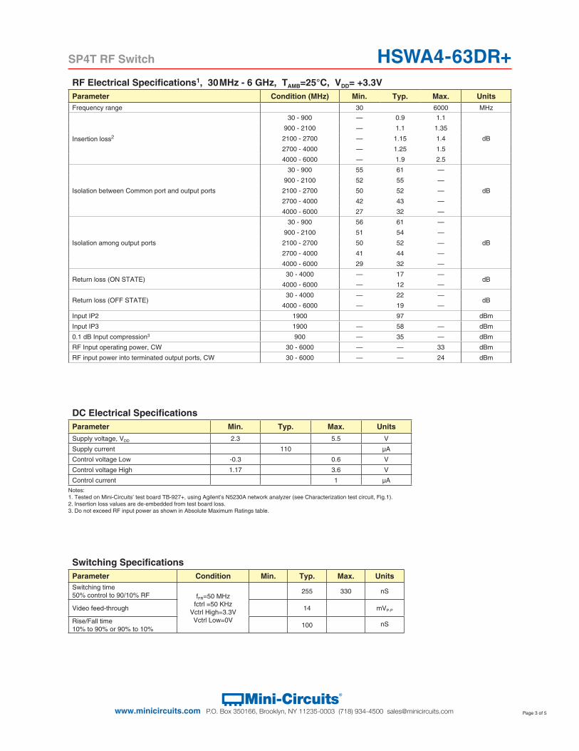
RF Electrical Specifications1, 30 MHz - 6 GHz, TAMB=25°C, VDD= +3.3V Parameter Condition (MHz) Min. Typ. Max. UnitsFrequency range 30 6000 MHz
Insertion loss2
30 - 900 — 0.9 1.1
dB
900 - 2100 — 1.1 1.35
2100 - 2700 — 1.15 1.4
2700 - 4000 — 1.25 1.5
4000 - 6000 — 1.9 2.5
Isolation between Common port and output ports
30 - 900 55 61 —
dB
900 - 2100 52 55 —
2100 - 2700 50 52 —
2700 - 4000 42 43 —
4000 - 6000 27 32 —
Isolation among output ports
30 - 900 56 61 —
dB
900 - 2100 51 54 —
2100 - 2700 50 52 —
2700 - 4000 41 44 —
4000 - 6000 29 32 —
Return loss (ON STATE)30 - 4000 — 17 —
dB4000 - 6000 — 12 —
Return loss (OFF STATE)30 - 4000 — 22 —
dB4000 - 6000 — 19 —
Input IP2 1900 97 dBm
Input IP3 1900 — 58 — dBm
0.1 dB Input compression3 900 — 35 — dBm
RF Input operating power, CW 30 - 6000 — — 33 dBm
RF input power into terminated output ports, CW 30 - 6000 — — 24 dBm
DC Electrical SpecificationsParameter Min. Typ. Max. UnitsSupply voltage, VDD 2.3 5.5 V
Supply current 110 µA
Control voltage Low -0.3 0.6 V
Control voltage High 1.17 3.6 V
Control current 1 µA
Switching SpecificationsParameter Condition Min. Typ. Max. UnitsSwitching time50% control to 90/10% RF fFR=50 MHz
fctrl =50 KHzVctrl High=3.3VVctrl Low=0V
255 330 nS
Video feed-through 14 mVP-P
Rise/Fall time10% to 90% or 90% to 10%
100 nS
Notes:1. Tested on Mini-Circuits’ test board TB-927+, using Agilent’s N5230A network analyzer (see Characterization test circuit, Fig.1).2. Insertion loss values are de-embedded from test board loss. 3. Do not exceed RF input power as shown in Absolute Maximum Ratings table.

SP4T RF Switch HSWA4-63DR+
Page 4 of 5
NotesA. Performance and quality attributes and conditions not expressly stated in this specification document are intended to be excluded and do not form a part of this specification document. B. Electrical specifications and performance data contained in this specification document are based on Mini-Circuit’s applicable established test performance criteria and measurement instructions. C. The parts covered by this specification document are subject to Mini-Circuits standard limited warranty and terms and conditions (collectively, “Standard Terms”); Purchasers of this part are entitled to the rights and benefits contained therein. For a full statement of the Standard Terms and the exclusive rights and remedies thereunder, please visit Mini-Circuits’ website at www.minicircuits.com/MCLStore/terms.jsp
Mini-Circuits®
www.minicircuits.com P.O. Box 350166, Brooklyn, NY 11235-0003 (718) 934-4500 [email protected]
Absolute Maximum Ratings4
Parameter RatingsOperating temperature -40°C to +105°C
Storage temperature -65°C to 150°C
VDD, Supply voltage -0.3 to 5.5V
Voltage control -0.3V Min. 3.6 Max.
RF Input power, CW 34 dBm
4. Operation of this device above any of these conditions may cause permanent damage.
Characterization Test Application Circuit
Figure 1. Block Diagram of test Circuit used for characterization (DUT soldered on Mini-Circuit’s TB-927+)
ParameterConditions
VDD=+2.3V and 5.5VControl= 0V and 3.3V
Test Equipment
Insertion loss, Isolation, Return loss and DC current
Pin=0 dBmKeysight N5242A Network Analyzer, E3631A power supply. Cblock: Internal to network Analyzer.
Switching time and DC CurrentRF frequency: 50 MHz at 0 dBm, Control frequency: 50 KHz
Keysight 54832B oscilloscope, 81110A pulse generator and E3631A power supply
Input IP3 +15 dBm / toneKeysight ES257D signal generators, E4416A power meter, N9020A Signal analyzer and E3631A power supply
Compression — Keysight N5242A Network Analyzer, E3631A power supply
TB-927+
Component Value Size
DUT HSWA4-63DR+ 4x4 mm
C2, C3, C4, C5 100pF
0402C6 1uF
R1, R2, R3, R5, R7, R9 0 Ohm
R4, R6, R8 1 MOhm
Truth Table- 3 Pin Control Truth Table- 2 Pin Control
Mode Control 3 Control 2 Control 1 Mode Control 2 Control 1RF COM-RF1 ON Low Low High RF COM-RF1 ON Low HighRF COM-RF2 ON Low High Low RF COM-RF2 ON High LowRF COM-RF3 ON Low High High RF COM-RF3 ON High High
High Low Low RF COM-RF4 ON Low LowLow Low Low
All off High Low HighAll off High High LowUnsupported High High High
State of Control VoltageState of Control
Voltage
RF COM-RF4 ON6. Pad 19= control 3 must be grounded.
6

SP4T RF Switch HSWA4-63DR+
Page 5 of 5
NotesA. Performance and quality attributes and conditions not expressly stated in this specification document are intended to be excluded and do not form a part of this specification document. B. Electrical specifications and performance data contained in this specification document are based on Mini-Circuit’s applicable established test performance criteria and measurement instructions. C. The parts covered by this specification document are subject to Mini-Circuits standard limited warranty and terms and conditions (collectively, “Standard Terms”); Purchasers of this part are entitled to the rights and benefits contained therein. For a full statement of the Standard Terms and the exclusive rights and remedies thereunder, please visit Mini-Circuits’ website at www.minicircuits.com/MCLStore/terms.jsp
Mini-Circuits®
www.minicircuits.com P.O. Box 350166, Brooklyn, NY 11235-0003 (718) 934-4500 [email protected]
ESD Rating Human Body Model (HBM): Class 2 (Pass 2000V) in accordance with MIL-STD-883, Method 3015
Charge Device Model (CDM): Class C1 (Pass 250V) in accordance with JESD22-C101
MSL RatingMoisture Sensitivity: MSL1 in accordance with IPC/JEDEC J-STD-020D
Additional Detailed Technical Information additional information is available on our dash board. To access this information click here
Performance DataData Table
Swept Graphs
Case Style DG984-1 Plastic package: exposed paddle Termination finish: NiPdAu
Tape & Reel
Standard quantities available on reel
F68
7” reels with 20, 50, 100, 200, 500 and 3000 devices
Suggested Layout for PCB Design PL-514
Evaluation Board TB-927+
Environmental Ratings ENV84
Product Marking
MCLHSWA4
24
1
Additional NotesA. Performance and quality attributes and conditions not expressly stated in this specification document are intended to be excluded and do not form a part of this specification document.
B. Electrical specifications and performance data contained in this specification document are based on Mini-Circuit’s applicable established test performance criteria and measurement instructions.
C. The parts covered by this specification document are subject to Mini-Circuits standard limited warranty and terms and conditions (collectively, “Standard Terms”); Purchasers of this part are entitled to the rights and benefits contained therein. For a full statement of the Standard Terms and the exclusive rights and remedies thereunder, please visit Mini-Circuits’ website at www.minicircuits.com/MCLStore/terms.jsp

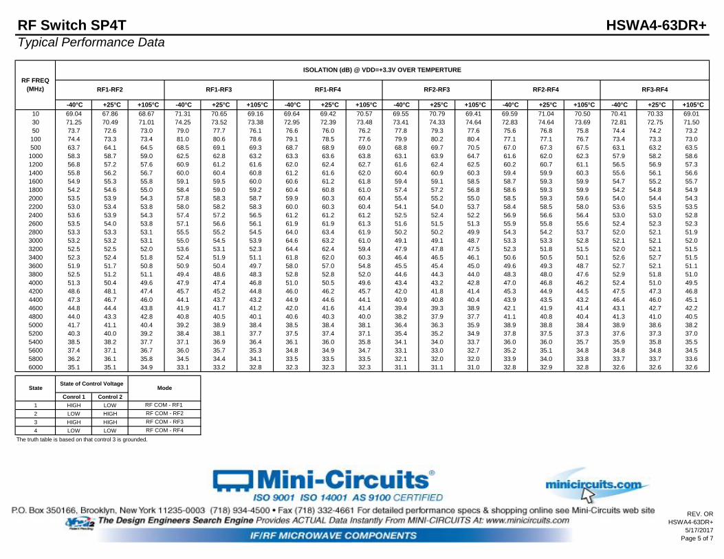
RF Switch SP4T HSWA4-63DR+Typical Performance Data
RF COM-
RF1
RF COM-
RF2
RF COM-
RF3
RF COM-
RF4
RF COM-
RF1
RF COM-
RF2
RF COM-
RF3
RF COM-
RF4 RF1-RF2 RF1-RF3 RF1-RF4 RF2-RF3 RF2-RF4 RF3-RF4
10 0.74 0.77 0.76 0.74 10 81.68 81.36 79.88 81.49 67.86 70.65 69.42 70.79 71.04 70.33
30 0.75 0.78 0.77 0.75 30 82.09 81.60 80.65 82.31 70.49 73.52 72.39 74.33 74.64 72.75
50 0.75 0.78 0.77 0.75 50 82.46 81.67 80.22 83.36 72.58 77.69 76.01 79.30 76.75 74.25
100 0.76 0.79 0.79 0.76 100 81.92 80.53 78.15 82.31 73.34 80.59 78.47 80.18 77.14 73.28
500 0.80 0.86 0.86 0.80 500 73.71 68.33 67.37 70.42 64.10 69.09 68.87 69.73 67.29 63.18
1000 0.88 0.96 0.96 0.87 1000 66.88 62.28 61.72 63.19 58.72 62.81 63.56 63.86 61.95 58.22
1200 0.92 1.01 1.00 0.91 1200 63.72 60.84 60.66 61.61 57.21 61.24 62.42 62.40 60.67 56.95
1400 0.95 1.04 1.04 0.94 1400 62.47 59.82 59.64 60.04 56.20 60.41 61.64 60.87 59.91 56.08
1600 0.98 1.06 1.05 0.96 1600 61.40 58.86 59.07 58.40 55.34 59.52 61.20 59.08 59.27 55.21
1800 0.99 1.03 1.02 0.98 1800 59.96 58.17 58.61 57.02 54.59 58.98 60.84 57.21 59.26 54.79
2000 0.99 0.99 0.97 0.96 2000 58.95 57.42 57.76 56.21 53.88 58.27 60.29 55.25 59.34 54.37
2200 0.94 0.96 0.96 0.94 2200 57.39 56.95 57.08 54.66 53.42 58.24 60.29 54.02 58.53 53.52
2400 0.92 1.01 1.02 0.91 2400 55.16 56.89 57.26 53.13 53.94 57.16 61.22 52.41 56.63 53.00
2600 0.91 1.13 1.12 0.91 2600 53.39 56.00 56.35 51.44 53.97 56.59 61.91 51.48 55.77 52.35
2800 0.93 1.18 1.16 0.91 2800 52.09 55.81 54.66 50.02 53.34 55.20 63.38 50.21 54.19 52.08
3000 0.94 1.15 1.11 0.91 3000 50.44 55.54 52.98 49.00 53.24 54.54 63.17 49.05 53.26 52.10
3200 0.95 1.08 1.04 0.91 3200 49.32 55.05 52.59 47.54 52.51 53.13 62.36 47.77 51.79 52.14
3400 1.00 1.04 1.01 0.94 3400 47.91 53.47 50.63 46.40 52.38 51.92 61.97 46.45 50.48 52.72
3600 1.05 1.05 1.03 0.99 3600 46.68 52.58 49.08 45.02 51.69 50.41 56.99 45.39 49.28 52.05
3800 1.14 1.10 1.08 1.06 3800 45.22 51.31 47.79 43.56 51.19 48.63 52.76 44.28 47.99 51.78
4000 1.17 1.15 1.15 1.08 4000 44.12 48.98 46.32 42.59 50.43 47.42 50.50 43.18 46.78 51.00
4200 1.13 1.24 1.25 1.07 4200 43.27 47.46 44.96 41.65 48.09 45.20 46.17 41.83 44.86 47.35
4400 1.04 1.38 1.37 1.03 4400 42.23 46.26 43.45 40.54 46.69 43.73 44.57 40.77 43.52 46.00
4600 1.06 1.55 1.49 1.10 4600 41.47 44.71 42.09 39.55 44.35 41.70 41.59 39.29 41.88 42.72
4800 1.25 1.62 1.57 1.31 4800 40.36 43.48 41.38 38.55 43.34 40.51 40.34 37.85 40.77 41.01
5000 1.64 1.69 1.63 1.70 5000 38.75 42.82 40.62 36.95 41.13 38.94 38.40 36.29 38.77 38.63
5200 2.00 1.77 1.79 2.04 5200 37.65 41.44 39.10 35.22 39.96 38.08 37.38 35.16 37.50 37.29
5400 2.16 1.88 2.00 2.24 5400 36.37 40.75 38.00 34.10 38.25 36.90 35.96 34.00 35.99 35.76
5600 2.16 1.99 2.11 2.23 5600 35.13 40.27 37.24 33.18 37.13 35.72 34.87 32.99 35.10 34.85
5800 2.02 2.06 2.13 2.16 5800 34.38 38.94 35.92 32.30 36.08 34.42 33.53 32.04 33.95 33.69
6000 1.90 2.10 2.11 2.08 6000 33.59 37.54 34.35 31.23 35.13 33.15 32.30 31.14 32.88 32.63
Conrol 1 Control 2
1 HIGH LOW
2 LOW HIGH
3 HIGH HIGH
4 LOW LOW
State of Control VoltageState Mode
INSERTION LOSS (dB)
VDD=+3.3V
The truth table is based on that control 3 is grounded.
VDD=+3.3V VDD=+3.3V
ISOLATION (dB)
RF COM - RF1
RF COM - RF2
RF COM - RF3
RF COM - RF4
RF FREQ
(MHz)
RF FREQ
(MHz)
REV. OR
HSWA4-63DR+
5/17/2017
Page 1 of 7

RF Switch SP4TTypical Performance Data
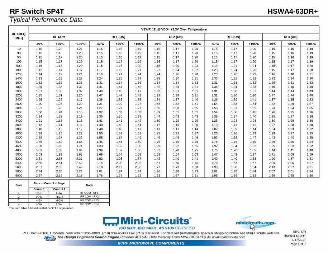
RF COM RF1 (ON) RF2 (ON) RF3 (ON) RF4 (ON) RF1 (OFF) RF2 (OFF) RF3 (OFF) RF4 (OFF)
10 1.20 1.16 1.17 1.17 1.16 10 1.13 1.14 1.14 1.13
30 1.18 1.16 1.17 1.17 1.16 30 1.13 1.13 1.14 1.13
50 1.17 1.16 1.17 1.17 1.16 50 1.13 1.13 1.14 1.13
100 1.17 1.17 1.17 1.17 1.17 100 1.13 1.13 1.13 1.13
500 1.18 1.17 1.20 1.21 1.17 500 1.11 1.09 1.09 1.11
1000 1.14 1.19 1.24 1.24 1.17 1000 1.05 1.05 1.05 1.08
1200 1.17 1.21 1.26 1.26 1.18 1200 1.04 1.10 1.10 1.08
1400 1.25 1.25 1.30 1.31 1.24 1400 1.07 1.16 1.16 1.12
1600 1.32 1.34 1.34 1.33 1.31 1600 1.13 1.20 1.20 1.17
1800 1.35 1.41 1.33 1.34 1.40 1800 1.18 1.24 1.25 1.23
2000 1.35 1.48 1.31 1.30 1.44 2000 1.24 1.24 1.23 1.29
2200 1.31 1.44 1.29 1.30 1.44 2200 1.29 1.21 1.18 1.33
2400 1.22 1.36 1.37 1.39 1.35 2400 1.29 1.14 1.12 1.35
2600 1.26 1.29 1.52 1.53 1.29 2600 1.29 1.04 1.06 1.34
2800 1.28 1.27 1.58 1.57 1.24 2800 1.24 1.07 1.12 1.31
3000 1.24 1.32 1.55 1.50 1.25 3000 1.18 1.18 1.22 1.27
3200 1.22 1.36 1.43 1.37 1.27 3200 1.12 1.27 1.33 1.22
3400 1.18 1.41 1.29 1.24 1.29 3400 1.05 1.36 1.37 1.19
3600 1.11 1.40 1.16 1.11 1.28 3600 1.10 1.38 1.39 1.21
3800 1.16 1.48 1.11 1.09 1.33 3800 1.19 1.36 1.36 1.27
4000 1.25 1.53 1.23 1.26 1.37 4000 1.30 1.28 1.25 1.35
4200 1.37 1.54 1.48 1.52 1.40 4200 1.38 1.18 1.13 1.44
4400 1.62 1.44 1.76 1.75 1.36 4400 1.46 1.04 1.03 1.49
4600 1.83 1.32 1.92 1.84 1.33 4600 1.50 1.09 1.16 1.52
4800 1.86 1.37 1.78 1.70 1.41 4800 1.50 1.24 1.29 1.52
5000 1.99 1.64 1.54 1.43 1.65 5000 1.46 1.35 1.43 1.46
5200 2.33 1.93 1.40 1.40 1.87 5200 1.36 1.41 1.47 1.39
5400 2.51 2.08 1.50 1.67 2.05 5400 1.26 1.44 1.46 1.29
5600 2.53 2.12 1.73 1.88 2.07 5600 1.16 1.39 1.38 1.19
5800 2.36 1.97 1.88 1.95 2.01 5800 1.06 1.34 1.25 1.11
6000 2.19 1.74 1.87 1.86 1.85 6000 1.08 1.20 1.13 1.12
Conrol 1 Control 2
1 HIGH LOW
2 LOW HIGH
3 HIGH HIGH
4 LOW LOW
HSWA4-63DR+
VDD=+3V
VSWR (:1)
StateState of Control Voltage
Mode
RF FREQ
(MHz)
RF FREQ
(MHz)VDD=+3V
RF COM - RF1
RF COM - RF2
RF COM - RF3
RF COM - RF4
VSWR (:1)
The truth table is based on that control 3 is grounded.
REV. OR
HSWA4-63DR+
5/17/2017
Page 2 of 7

RF Switch SP4T HSWA4-63DR+Typical Performance Data
-40°C +25°C +105°C -40°C +25°C +105°C -40°C +25°C +105°C -40°C +25°C +105°C
10 0.67 0.74 0.87 0.69 0.77 0.90 0.69 0.76 0.90 0.67 0.74 0.87
30 0.67 0.75 0.87 0.69 0.78 0.91 0.69 0.77 0.90 0.67 0.75 0.87
50 0.67 0.75 0.87 0.70 0.78 0.91 0.69 0.77 0.90 0.67 0.75 0.87
100 0.68 0.76 0.88 0.70 0.79 0.92 0.70 0.79 0.91 0.67 0.76 0.88
500 0.68 0.80 0.95 0.74 0.86 1.02 0.73 0.86 1.01 0.68 0.80 0.95
1000 0.72 0.88 1.05 0.80 0.96 1.15 0.79 0.96 1.14 0.72 0.87 1.05
1200 0.75 0.92 1.10 0.83 1.01 1.20 0.81 1.00 1.19 0.74 0.91 1.09
1400 0.77 0.95 1.13 0.85 1.04 1.24 0.85 1.04 1.23 0.76 0.94 1.13
1600 0.79 0.98 1.17 0.87 1.06 1.25 0.84 1.05 1.24 0.77 0.96 1.16
1800 0.80 0.99 1.18 0.84 1.03 1.22 0.82 1.02 1.21 0.79 0.98 1.16
2000 0.80 0.99 1.17 0.79 0.99 1.19 0.76 0.97 1.18 0.77 0.96 1.15
2200 0.75 0.94 1.13 0.74 0.96 1.17 0.74 0.96 1.17 0.75 0.94 1.13
2400 0.71 0.92 1.12 0.78 1.01 1.24 0.77 1.02 1.25 0.71 0.91 1.12
2600 0.70 0.91 1.13 0.89 1.13 1.34 0.87 1.12 1.35 0.70 0.91 1.13
2800 0.69 0.93 1.15 0.94 1.18 1.39 0.90 1.16 1.39 0.67 0.91 1.15
3000 0.70 0.94 1.18 0.91 1.15 1.37 0.86 1.11 1.34 0.67 0.91 1.15
3200 0.70 0.95 1.20 0.82 1.08 1.33 0.76 1.04 1.29 0.65 0.91 1.16
3400 0.74 1.00 1.25 0.76 1.04 1.30 0.73 1.01 1.28 0.68 0.94 1.20
3600 0.78 1.05 1.32 0.77 1.05 1.33 0.73 1.03 1.30 0.72 0.99 1.26
3800 0.86 1.14 1.41 0.80 1.10 1.38 0.76 1.08 1.37 0.78 1.06 1.33
4000 0.90 1.17 1.44 0.83 1.15 1.44 0.82 1.15 1.46 0.80 1.08 1.36
4200 0.85 1.13 1.40 0.92 1.24 1.52 0.92 1.25 1.54 0.78 1.07 1.35
4400 0.73 1.04 1.33 1.06 1.38 1.64 1.02 1.37 1.65 0.71 1.03 1.33
4600 0.74 1.06 1.35 1.23 1.55 1.82 1.16 1.49 1.77 0.77 1.10 1.41
4800 0.92 1.25 1.58 1.27 1.62 1.96 1.20 1.57 1.90 0.97 1.31 1.64
5000 1.31 1.64 1.95 1.32 1.69 2.03 1.24 1.63 1.97 1.37 1.70 2.01
5200 1.60 2.00 2.35 1.36 1.77 2.16 1.35 1.79 2.18 1.65 2.04 2.40
5400 1.79 2.16 2.52 1.47 1.88 2.25 1.57 2.00 2.39 1.84 2.24 2.61
5600 1.76 2.16 2.56 1.56 1.99 2.37 1.67 2.11 2.53 1.81 2.23 2.65
5800 1.63 2.02 2.41 1.67 2.06 2.47 1.71 2.13 2.55 1.76 2.16 2.58
6000 1.50 1.90 2.35 1.68 2.10 2.52 1.68 2.11 2.54 1.67 2.08 2.54
Conrol 1 Control 2
1 HIGH LOW
2 LOW HIGH
3 HIGH HIGH
4 LOW LOW
RF COM - RF1
RF COM-RF1 RF COM-RF2
RF COM - RF2
RF COM - RF3
RF COM - RF4
The truth table is based on that control 3 is grounded.
INSERTION LOSS (dB) @ VDD=+3.3V OVER TEMPERTURE
RF COM-RF3 RF COM-RF4
StateState of Control Voltage
Mode
RF FREQ
(MHz)
REV. OR
HSWA4-63DR+
5/17/2017
Page 3 of 7

RF Switch SP4T HSWA4-63DR+Typical Performance Data
-40°C +25°C +105°C -40°C +25°C +105°C -40°C +25°C +105°C -40°C +25°C +105°C
10 84.11 81.68 80.05 83.68 81.36 84.90 86.12 79.88 79.96 83.15 81.49 84.32
30 84.85 82.09 81.35 83.30 81.60 83.32 84.45 80.65 79.57 84.29 82.31 84.38
50 85.1 82.5 82.3 82.8 81.7 81.6 82.8 80.2 79.2 85.2 83.4 84.2
100 83.6 81.9 82.3 81.2 80.5 78.9 79.0 78.2 77.6 81.7 82.3 83.4
500 72.0 73.7 76.6 68.3 68.3 68.2 67.6 67.4 67.0 69.4 70.4 72.0
1000 65.6 66.9 69.2 62.2 62.3 62.2 61.8 61.7 61.4 62.3 63.2 64.5
1200 62.7 63.7 65.5 60.8 60.8 60.7 60.7 60.7 60.4 60.8 61.6 62.9
1400 61.3 62.5 63.9 59.7 59.8 59.6 59.6 59.6 59.4 59.3 60.0 61.1
1600 60.4 61.4 62.7 58.8 58.9 58.7 59.1 59.1 58.8 57.7 58.4 59.3
1800 59.1 60.0 61.0 58.1 58.2 58.0 58.6 58.6 58.3 56.4 57.0 57.9
2000 58.3 58.9 60.0 57.4 57.4 57.2 57.7 57.8 57.5 55.8 56.2 56.8
2200 56.8 57.4 58.1 56.8 57.0 57.1 56.9 57.1 57.0 54.3 54.7 55.3
2400 54.8 55.2 55.7 56.7 56.9 56.5 57.1 57.3 57.2 52.7 53.1 53.4
2600 53.0 53.4 53.9 56.0 56.0 55.8 56.1 56.3 56.1 51.3 51.4 51.8
2800 51.8 52.1 52.4 55.7 55.8 55.0 54.8 54.7 54.3 49.8 50.0 50.3
3000 50.2 50.4 50.6 55.8 55.5 54.7 53.2 53.0 52.9 48.7 49.0 49.0
3200 49.1 49.3 49.4 55.5 55.1 53.9 52.5 52.6 52.1 47.5 47.5 47.5
3400 47.9 47.9 48.0 53.9 53.5 52.3 50.7 50.6 49.9 46.4 46.4 46.6
3600 46.6 46.7 46.7 53.2 52.6 51.6 49.4 49.1 48.7 44.9 45.0 44.9
3800 45.0 45.2 45.1 52.9 51.3 51.0 48.3 47.8 47.7 43.6 43.6 43.5
4000 43.9 44.1 44.0 49.5 49.0 48.1 46.6 46.3 45.8 42.5 42.6 42.5
4200 43.1 43.3 43.1 48.0 47.5 46.8 45.0 45.0 44.4 41.7 41.6 41.6
4400 42.4 42.2 42.2 46.6 46.3 45.4 43.6 43.4 42.9 40.7 40.5 40.5
4600 41.4 41.5 41.1 45.2 44.7 44.1 42.4 42.1 41.9 39.6 39.6 39.3
4800 40.3 40.4 40.1 43.6 43.5 42.7 41.5 41.4 40.8 38.6 38.5 38.3
5000 39.0 38.7 38.6 43.3 42.8 42.0 41.0 40.6 40.2 37.1 36.9 36.7
5200 37.8 37.6 37.5 42.1 41.4 40.7 39.4 39.1 38.5 35.2 35.2 35.0
5400 36.5 36.4 36.3 41.3 40.8 40.1 38.3 38.0 37.7 34.0 34.1 34.1
5600 35.1 35.1 35.0 40.7 40.3 39.5 37.5 37.2 36.7 33.1 33.2 33.1
5800 34.4 34.4 34.3 39.5 38.9 38.2 36.1 35.9 35.5 32.3 32.3 32.4
6000 33.6 33.6 33.5 38.0 37.5 36.9 34.5 34.3 34.0 31.2 31.2 31.3
Conrol 1 Control 2
1 HIGH LOW
2 LOW HIGH
3 HIGH HIGH
4 LOW LOW
RF FREQ
(MHz) RF COM-RF1 RF COM-RF2
ISOLATION (dB) @ VDD=+3.3V OVER TEMPERTURE
StateState of Control Voltage
Mode
The truth table is based on that control 3 is grounded.
RF COM - RF1
RF COM - RF2
RF COM-RF3 RF COM-RF4
RF COM - RF3
RF COM - RF4
REV. OR
HSWA4-63DR+
5/17/2017
Page 4 of 7
RF Switch SP4T HSWA4-63DR+Typical Performance Data
-40°C +25°C +105°C -40°C +25°C +105°C -40°C +25°C +105°C -40°C +25°C +105°C -40°C +25°C +105°C -40°C +25°C +105°C
10 69.04 67.86 68.67 71.31 70.65 69.16 69.64 69.42 70.57 69.55 70.79 69.41 69.59 71.04 70.50 70.41 70.33 69.01
30 71.25 70.49 71.01 74.25 73.52 73.38 72.95 72.39 73.48 73.41 74.33 74.64 72.83 74.64 73.69 72.81 72.75 71.50
50 73.7 72.6 73.0 79.0 77.7 76.1 76.6 76.0 76.2 77.8 79.3 77.6 75.6 76.8 75.8 74.4 74.2 73.2
100 74.4 73.3 73.4 81.0 80.6 78.6 79.1 78.5 77.6 79.9 80.2 80.4 77.1 77.1 76.7 73.4 73.3 73.0
500 63.7 64.1 64.5 68.5 69.1 69.3 68.7 68.9 69.0 68.8 69.7 70.5 67.0 67.3 67.5 63.1 63.2 63.5
1000 58.3 58.7 59.0 62.5 62.8 63.2 63.3 63.6 63.8 63.1 63.9 64.7 61.6 62.0 62.3 57.9 58.2 58.6
1200 56.8 57.2 57.6 60.9 61.2 61.6 62.0 62.4 62.7 61.6 62.4 62.5 60.2 60.7 61.1 56.5 56.9 57.3
1400 55.8 56.2 56.7 60.0 60.4 60.8 61.2 61.6 62.0 60.4 60.9 60.3 59.4 59.9 60.3 55.6 56.1 56.6
1600 54.9 55.3 55.8 59.1 59.5 60.0 60.6 61.2 61.8 59.4 59.1 58.5 58.7 59.3 59.9 54.7 55.2 55.7
1800 54.2 54.6 55.0 58.4 59.0 59.2 60.4 60.8 61.0 57.4 57.2 56.8 58.6 59.3 59.9 54.2 54.8 54.9
2000 53.5 53.9 54.3 57.8 58.3 58.7 59.9 60.3 60.4 55.4 55.2 55.0 58.5 59.3 59.6 54.0 54.4 54.3
2200 53.0 53.4 53.8 58.0 58.2 58.3 60.0 60.3 60.4 54.1 54.0 53.7 58.4 58.5 58.0 53.6 53.5 53.5
2400 53.6 53.9 54.3 57.4 57.2 56.5 61.2 61.2 61.2 52.5 52.4 52.2 56.9 56.6 56.4 53.0 53.0 52.8
2600 53.5 54.0 53.8 57.1 56.6 56.1 61.9 61.9 61.3 51.6 51.5 51.3 55.9 55.8 55.6 52.4 52.3 52.3
2800 53.3 53.3 53.1 55.5 55.2 54.5 64.0 63.4 61.9 50.2 50.2 49.9 54.3 54.2 53.7 52.0 52.1 51.9
3000 53.2 53.2 53.1 55.0 54.5 53.9 64.6 63.2 61.0 49.1 49.1 48.7 53.3 53.3 52.8 52.1 52.1 52.0
3200 52.5 52.5 52.0 53.6 53.1 52.3 64.4 62.4 59.4 47.9 47.8 47.5 52.3 51.8 51.5 52.0 52.1 51.5
3400 52.3 52.4 51.8 52.4 51.9 51.1 61.8 62.0 60.3 46.4 46.5 46.1 50.6 50.5 50.1 52.6 52.7 51.5
3600 51.9 51.7 50.8 50.9 50.4 49.7 58.0 57.0 54.8 45.5 45.4 45.0 49.6 49.3 48.7 52.7 52.1 51.1
3800 52.5 51.2 51.1 49.4 48.6 48.3 52.8 52.8 52.0 44.6 44.3 44.0 48.3 48.0 47.6 52.9 51.8 51.0
4000 51.3 50.4 49.6 47.9 47.4 46.8 51.0 50.5 49.6 43.4 43.2 42.8 47.0 46.8 46.2 52.4 51.0 49.5
4200 48.6 48.1 47.4 45.7 45.2 44.8 46.0 46.2 45.7 42.0 41.8 41.4 45.3 44.9 44.5 47.5 47.3 46.8
4400 47.3 46.7 46.0 44.1 43.7 43.2 44.9 44.6 44.1 40.9 40.8 40.4 43.9 43.5 43.2 46.4 46.0 45.1
4600 44.8 44.4 43.8 41.9 41.7 41.2 42.0 41.6 41.4 39.4 39.3 38.9 42.1 41.9 41.4 43.1 42.7 42.2
4800 44.0 43.3 42.8 40.8 40.5 40.1 40.6 40.3 40.0 38.2 37.9 37.7 41.1 40.8 40.4 41.3 41.0 40.5
5000 41.7 41.1 40.4 39.2 38.9 38.4 38.5 38.4 38.1 36.4 36.3 35.9 38.9 38.8 38.4 38.9 38.6 38.2
5200 40.3 40.0 39.2 38.4 38.1 37.7 37.5 37.4 37.1 35.4 35.2 34.9 37.8 37.5 37.3 37.6 37.3 37.0
5400 38.5 38.2 37.7 37.1 36.9 36.4 36.1 36.0 35.8 34.1 34.0 33.7 36.0 36.0 35.7 35.9 35.8 35.5
5600 37.4 37.1 36.7 36.0 35.7 35.3 34.8 34.9 34.7 33.1 33.0 32.7 35.2 35.1 34.8 34.8 34.8 34.5
5800 36.2 36.1 35.8 34.5 34.4 34.1 33.5 33.5 33.5 32.1 32.0 32.0 33.9 34.0 33.8 33.7 33.7 33.6
6000 35.1 35.1 34.9 33.1 33.2 32.8 32.3 32.3 32.3 31.1 31.1 31.0 32.8 32.9 32.8 32.6 32.6 32.6
Conrol 1 Control 2
1 HIGH LOW
2 LOW HIGH
3 HIGH HIGH
4 LOW LOW
The truth table is based on that control 3 is grounded.
ISOLATION (dB) @ VDD=+3.3V OVER TEMPERTURE
RF1-RF4 RF2-RF3RF1-RF2 RF1-RF3 RF3-RF4
RF COM - RF2
RF COM - RF3
RF COM - RF4
RF2-RF4
RF FREQ
(MHz)
StateState of Control Voltage
Mode
RF COM - RF1
REV. OR
HSWA4-63DR+
5/17/2017
Page 5 of 7
RF Switch SP4T HSWA4-63DR+Typical Performance Data
-40°C +25°C +105°C -40°C +25°C +105°C -40°C +25°C +105°C -40°C +25°C +105°C -40°C +25°C +105°C
10 1.16 1.20 1.21 1.15 1.16 1.19 1.15 1.17 1.20 1.15 1.17 1.20 1.15 1.16 1.19
30 1.15 1.18 1.20 1.15 1.16 1.19 1.15 1.17 1.20 1.15 1.17 1.20 1.15 1.16 1.19
50 1.15 1.17 1.20 1.15 1.16 1.19 1.15 1.17 1.20 1.15 1.17 1.20 1.15 1.16 1.19
100 1.15 1.17 1.20 1.15 1.17 1.19 1.16 1.17 1.20 1.15 1.17 1.20 1.15 1.17 1.19
500 1.16 1.18 1.20 1.15 1.17 1.20 1.18 1.20 1.23 1.19 1.21 1.24 1.15 1.17 1.20
1000 1.12 1.14 1.17 1.17 1.19 1.21 1.22 1.24 1.27 1.23 1.24 1.26 1.15 1.17 1.20
1200 1.14 1.17 1.21 1.19 1.21 1.24 1.24 1.26 1.28 1.23 1.26 1.29 1.16 1.18 1.21
1400 1.23 1.25 1.27 1.24 1.25 1.28 1.28 1.30 1.31 1.30 1.31 1.32 1.22 1.24 1.26
1600 1.32 1.32 1.33 1.31 1.34 1.36 1.34 1.34 1.33 1.31 1.33 1.32 1.29 1.31 1.33
1800 1.35 1.35 1.33 1.41 1.41 1.42 1.35 1.33 1.31 1.36 1.34 1.33 1.40 1.40 1.40
2000 1.37 1.35 1.32 1.49 1.48 1.47 1.33 1.31 1.31 1.31 1.30 1.31 1.44 1.44 1.43
2200 1.35 1.31 1.26 1.47 1.44 1.41 1.29 1.29 1.31 1.31 1.30 1.30 1.47 1.44 1.40
2400 1.25 1.22 1.17 1.38 1.36 1.35 1.34 1.37 1.40 1.36 1.39 1.41 1.37 1.35 1.33
2600 1.30 1.26 1.20 1.31 1.29 1.27 1.53 1.52 1.51 1.54 1.53 1.54 1.32 1.29 1.27
2800 1.32 1.28 1.21 1.27 1.27 1.27 1.60 1.58 1.55 1.58 1.57 1.55 1.23 1.24 1.25
3000 1.30 1.24 1.16 1.32 1.32 1.33 1.59 1.55 1.51 1.54 1.50 1.45 1.26 1.25 1.26
3200 1.24 1.22 1.19 1.35 1.36 1.38 1.44 1.43 1.43 1.38 1.37 1.40 1.25 1.27 1.28
3400 1.21 1.18 1.15 1.41 1.41 1.42 1.30 1.29 1.29 1.25 1.24 1.24 1.30 1.29 1.30
3600 1.12 1.11 1.11 1.40 1.40 1.44 1.17 1.16 1.20 1.13 1.11 1.11 1.27 1.28 1.30
3800 1.18 1.16 1.12 1.48 1.48 1.47 1.11 1.11 1.14 1.07 1.09 1.14 1.34 1.33 1.32
4000 1.28 1.25 1.22 1.55 1.53 1.51 1.21 1.23 1.27 1.25 1.26 1.33 1.38 1.37 1.35
4200 1.39 1.37 1.32 1.58 1.54 1.49 1.49 1.48 1.46 1.53 1.52 1.47 1.43 1.40 1.35
4400 1.66 1.62 1.56 1.45 1.44 1.40 1.79 1.76 1.69 1.75 1.75 1.69 1.36 1.36 1.34
4600 1.90 1.83 1.74 1.33 1.32 1.30 1.99 1.92 1.85 1.92 1.84 1.82 1.35 1.33 1.32
4800 1.89 1.86 1.84 1.39 1.37 1.36 1.82 1.78 1.75 1.76 1.70 1.65 1.44 1.41 1.40
5000 2.03 1.99 1.93 1.69 1.64 1.58 1.59 1.54 1.53 1.47 1.43 1.37 1.71 1.65 1.59
5200 2.31 2.33 2.31 1.93 1.93 1.87 1.42 1.40 1.41 1.40 1.40 1.38 1.90 1.87 1.81
5400 2.56 2.51 2.43 2.14 2.08 2.02 1.51 1.50 1.45 1.70 1.67 1.67 2.09 2.05 1.97
5600 2.57 2.53 2.49 2.18 2.12 2.06 1.77 1.73 1.68 1.93 1.88 1.84 2.13 2.07 2.01
5800 2.44 2.36 2.28 2.01 1.97 1.89 1.96 1.88 1.83 2.01 1.95 1.84 2.07 2.01 1.94
6000 2.27 2.19 2.16 1.78 1.74 1.72 1.92 1.87 1.81 1.95 1.86 1.82 1.89 1.85 1.80
Conrol 1 Control 2
1 HIGH LOW
2 LOW HIGH
3 HIGH HIGH
4 LOW LOW
The truth table is based on that control 3 is grounded.
VSWR (:1) @ VDD= +3.3V Over Temperature
RF2 (ON)RF FREQ
(MHz)
RF COM - RF4
RF COM RF1 (ON) RF3 (ON) RF4 (ON)
RF COM - RF3
StateState of Control Voltage
Mode
RF COM - RF1
RF COM - RF2
REV. OR
HSWA4-63DR+
5/17/2017
Page 6 of 7

RF Switch SP4T HSWA4-63DR+Typical Performance Data
-40°C +25°C +105°C -40°C +25°C +105°C -40°C +25°C +105°C -40°C +25°C +105°C
10 1.25 1.13 1.01 1.26 1.14 1.01 1.26 1.14 1.01 1.25 1.13 1.01
30 1.25 1.13 1.01 1.26 1.13 1.01 1.26 1.14 1.01 1.25 1.13 1.01
50 1.25 1.13 1.01 1.25 1.13 1.01 1.26 1.14 1.01 1.25 1.13 1.01
100 1.24 1.13 1.01 1.25 1.13 1.00 1.25 1.13 1.00 1.24 1.13 1.01
500 1.23 1.11 1.02 1.21 1.09 1.04 1.21 1.09 1.04 1.23 1.11 1.03
1000 1.16 1.05 1.07 1.14 1.05 1.12 1.13 1.05 1.11 1.18 1.08 1.09
1200 1.14 1.04 1.11 1.16 1.10 1.14 1.17 1.10 1.16 1.17 1.08 1.11
1400 1.14 1.07 1.13 1.21 1.16 1.17 1.21 1.16 1.17 1.18 1.12 1.16
1600 1.17 1.13 1.17 1.28 1.20 1.15 1.28 1.20 1.16 1.21 1.17 1.19
1800 1.23 1.18 1.20 1.34 1.24 1.15 1.34 1.25 1.17 1.28 1.23 1.23
2000 1.31 1.24 1.21 1.37 1.24 1.10 1.37 1.23 1.09 1.35 1.29 1.25
2200 1.38 1.29 1.22 1.35 1.21 1.05 1.31 1.18 1.04 1.42 1.33 1.26
2400 1.40 1.29 1.18 1.28 1.14 1.01 1.26 1.12 1.04 1.46 1.35 1.25
2600 1.42 1.29 1.16 1.17 1.04 1.08 1.16 1.06 1.12 1.47 1.34 1.22
2800 1.37 1.24 1.11 1.11 1.07 1.14 1.16 1.12 1.16 1.45 1.31 1.19
3000 1.32 1.18 1.04 1.19 1.18 1.21 1.24 1.22 1.24 1.40 1.27 1.15
3200 1.25 1.12 1.01 1.32 1.27 1.23 1.38 1.33 1.29 1.35 1.22 1.14
3400 1.14 1.05 1.10 1.46 1.36 1.27 1.47 1.37 1.24 1.28 1.19 1.15
3600 1.14 1.10 1.16 1.52 1.38 1.24 1.53 1.39 1.27 1.28 1.21 1.19
3800 1.21 1.19 1.23 1.51 1.36 1.21 1.53 1.36 1.19 1.33 1.27 1.25
4000 1.35 1.30 1.30 1.44 1.28 1.12 1.39 1.25 1.08 1.42 1.35 1.30
4200 1.44 1.38 1.34 1.31 1.18 1.07 1.25 1.13 1.07 1.53 1.44 1.35
4400 1.57 1.46 1.37 1.15 1.04 1.06 1.14 1.03 1.12 1.62 1.49 1.38
4600 1.64 1.50 1.36 1.10 1.09 1.16 1.17 1.16 1.22 1.67 1.52 1.37
4800 1.64 1.50 1.34 1.27 1.24 1.23 1.32 1.29 1.25 1.66 1.52 1.36
5000 1.62 1.46 1.30 1.42 1.35 1.30 1.54 1.43 1.38 1.60 1.46 1.30
5200 1.49 1.36 1.21 1.53 1.41 1.29 1.62 1.47 1.33 1.54 1.39 1.24
5400 1.36 1.26 1.15 1.60 1.44 1.31 1.61 1.46 1.29 1.40 1.29 1.16
5600 1.25 1.16 1.14 1.53 1.39 1.23 1.54 1.38 1.26 1.32 1.19 1.06
5800 1.09 1.06 1.14 1.49 1.34 1.23 1.37 1.25 1.13 1.24 1.11 1.03
6000 1.07 1.08 1.18 1.29 1.20 1.14 1.21 1.13 1.16 1.23 1.12 1.10
Conrol 1 Control 2
1 HIGH LOW
2 LOW HIGH
3 HIGH HIGH
4 LOW LOW RF COM - RF4
RF FREQ
(MHz)
VSWR (:1) @ VDD= +3.3V Over Temperature
RF1 (OFF) RF2 (OFF) RF3 (OFF) RF4 (OFF)
StateState of Control Voltage
Mode
RF COM - RF1
RF COM - RF2
RF COM - RF3
The truth table is based on that control 3 is grounded.
REV. OR
HSWA4-63DR+
5/17/2017
Page 7 of 7

RF Switch SP4T HSWA4-63DR+
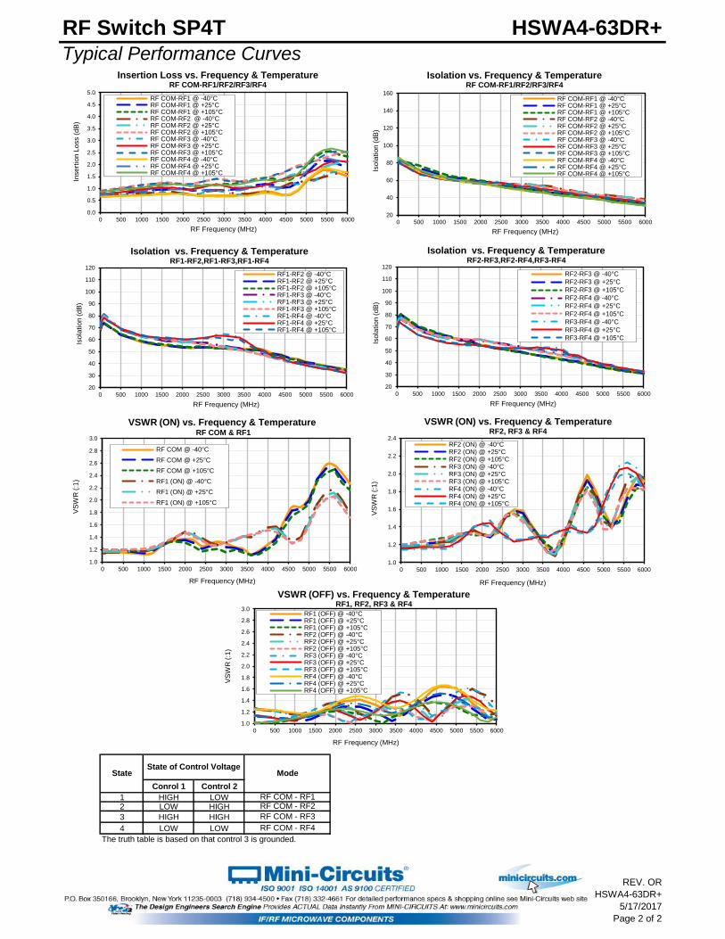
Typical Performance Curves
Conrol 1 Control 2
1 HIGH LOW
2 LOW HIGH
3 HIGH HIGH
4 LOW LOW
The truth table is based on that control 3 is grounded.
RF COM - RF3
StateState of Control Voltage
Mode
RF COM - RF1
RF COM - RF4
RF COM - RF2
0.0
0.5
1.0
1.5
2.0
2.5
3.0
0 500 1000 1500 2000 2500 3000 3500 4000 4500 5000 5500 6000
Inse
rtio
n L
oss (
dB
)
RF Frequency (MHz)
INSERTION LOSS RF COM-RF1, RF COM-RF2, RF COM-RF3 & RF COM-RF4
RF COM-RF1 @ VDD=+3.3V
RF COM-RF2 @ VDD=+3.3V
RF COM-RF3 @ VDD=+3.3V
RF COM-RF4 @ VDD=+3.3V
1.0
1.2
1.4
1.6
1.8
2.0
2.2
2.4
2.6
2.8
3.0
0 500 1000 1500 2000 2500 3000 3500 4000 4500 5000 5500 6000
VS
WR
(:1
)
RF Frequency (MHz)
VSWR (ON)RF COM,RF1,RF2,RF3,RF4
RF COM
RF1 (ON)
RF2 (ON)
RF3 (ON)
RF4 (ON)
1.0
1.1
1.2
1.3
1.4
1.5
1.6
1.7
1.8
0 500 1000 1500 2000 2500 3000 3500 4000 4500 5000 5500 6000
VS
WR
(:1
)
RF Frequency (MHz)
VSWR (OFF)RF1,RF2,RF3,RF4
RF1 (OFF)
RF2 (OFF)
RF3 (OFF)
RF4 (OFF)
0
10
20
30
40
50
60
70
80
90
100
0 500 1000 1500 2000 2500 3000 3500 4000 4500 5000 5500 6000
Iso
latio
n (
dB
)
RF Frequency (MHz)
ISOLATION RF COM-RF1, RF COM-RF1, RF COM-RF3 & RF COM-RF4
RF COM-RF1 @ VDD=+3.3V
RF COM-RF2 @ VDD=+3.3V
RF COM-RF3 @ VDD=+3.3V
RF COM-RF4 @ VDD=+3.3V
0
10
20
30
40
50
60
70
80
90
100
0 500 1000 1500 2000 2500 3000 3500 4000 4500 5000 5500 6000
Iso
latio
n (
dB
)
RF Frequency (MHz)
ISOLATION RF1-RF2,RF1-RF3,RF1-RF4,RF2-RF3,RF2-RF4 & RF3-RF4
RF1-RF2
RF1-RF3
RF1-RF4
RF2-RF3
RF2-RF4
RF3-RF4
REV. OR
HSWA4-63DR+
5/17/2017
Page 1 of 2
RF Switch SP4T HSWA4-63DR+
Typical Performance Curves
Conrol 1 Control 2
1 HIGH LOW2 LOW HIGH
3 HIGH HIGH
4 LOW LOW
RF COM - RF1
The truth table is based on that control 3 is grounded.
RF COM - RF2
RF COM - RF3
RF COM - RF4
StateState of Control Voltage
Mode
0.0
0.5
1.0
1.5
2.0
2.5
3.0
3.5
4.0
4.5
5.0
0 500 1000 1500 2000 2500 3000 3500 4000 4500 5000 5500 6000
Inse
rtio
n L
oss (
dB
)
RF Frequency (MHz)
Insertion Loss vs. Frequency & Temperature RF COM-RF1/RF2/RF3/RF4
RF COM-RF1 @ -40°CRF COM-RF1 @ +25°CRF COM-RF1 @ +105°CRF COM-RF2 @ -40°CRF COM-RF2 @ +25°CRF COM-RF2 @ +105°CRF COM-RF3 @ -40°CRF COM-RF3 @ +25°CRF COM-RF3 @ +105°CRF COM-RF4 @ -40°CRF COM-RF4 @ +25°CRF COM-RF4 @ +105°C
20
30
40
50
60
70
80
90
100
110
120
0 500 1000 1500 2000 2500 3000 3500 4000 4500 5000 5500 6000
Iso
latio
n (
dB
)
RF Frequency (MHz)
Isolation vs. Frequency & TemperatureRF1-RF2,RF1-RF3,RF1-RF4
RF1-RF2 @ -40°CRF1-RF2 @ +25°CRF1-RF2 @ +105°CRF1-RF3 @ -40°CRF1-RF3 @ +25°CRF1-RF3 @ +105°CRF1-RF4 @ -40°CRF1-RF4 @ +25°CRF1-RF4 @ +105°C
1.0
1.2
1.4
1.6
1.8
2.0
2.2
2.4
2.6
2.8
3.0
0 500 1000 1500 2000 2500 3000 3500 4000 4500 5000 5500 6000
VS
WR
(:1
)
RF Frequency (MHz)
VSWR (ON) vs. Frequency & Temperature RF COM & RF1
RF COM @ -40°C
RF COM @ +25°C
RF COM @ +105°C
RF1 (ON) @ -40°C
RF1 (ON) @ +25°C
RF1 (ON) @ +105°C
1.0
1.2
1.4
1.6
1.8
2.0
2.2
2.4
0 500 1000 1500 2000 2500 3000 3500 4000 4500 5000 5500 6000
VS
WR
(:1
)
RF Frequency (MHz)
VSWR (ON) vs. Frequency & Temperature RF2, RF3 & RF4
RF2 (ON) @ -40°CRF2 (ON) @ +25°CRF2 (ON) @ +105°CRF3 (ON) @ -40°CRF3 (ON) @ +25°CRF3 (ON) @ +105°CRF4 (ON) @ -40°CRF4 (ON) @ +25°CRF4 (ON) @ +105°C
20
40
60
80
100
120
140
160
0 500 1000 1500 2000 2500 3000 3500 4000 4500 5000 5500 6000
Iso
latio
n (
dB
)
RF Frequency (MHz)
Isolation vs. Frequency & Temperature RF COM-RF1/RF2/RF3/RF4
RF COM-RF1 @ -40°CRF COM-RF1 @ +25°CRF COM-RF1 @ +105°CRF COM-RF2 @ -40°CRF COM-RF2 @ +25°CRF COM-RF2 @ +105°CRF COM-RF3 @ -40°CRF COM-RF3 @ +25°CRF COM-RF3 @ +105°CRF COM-RF4 @ -40°CRF COM-RF4 @ +25°CRF COM-RF4 @ +105°C
20
30
40
50
60
70
80
90
100
110
120
0 500 1000 1500 2000 2500 3000 3500 4000 4500 5000 5500 6000
Iso
latio
n (
dB
)
RF Frequency (MHz)
Isolation vs. Frequency & TemperatureRF2-RF3,RF2-RF4,RF3-RF4
RF2-RF3 @ -40°C
RF2-RF3 @ +25°C
RF2-RF3 @ +105°C
RF2-RF4 @ -40°C
RF2-RF4 @ +25°C
RF2-RF4 @ +105°C
RF3-RF4 @ -40°C
RF3-RF4 @ +25°C
RF3-RF4 @ +105°C
1.0
1.2
1.4
1.6
1.8
2.0
2.2
2.4
2.6
2.8
3.0
0 500 1000 1500 2000 2500 3000 3500 4000 4500 5000 5500 6000
VS
WR
(:1
)
RF Frequency (MHz)
VSWR (OFF) vs. Frequency & Temperature RF1, RF2, RF3 & RF4
RF1 (OFF) @ -40°CRF1 (OFF) @ +25°CRF1 (OFF) @ +105°CRF2 (OFF) @ -40°CRF2 (OFF) @ +25°CRF2 (OFF) @ +105°CRF3 (OFF) @ -40°CRF3 (OFF) @ +25°CRF3 (OFF) @ +105°CRF4 (OFF) @ -40°CRF4 (OFF) @ +25°CRF4 (OFF) @ +105°C
REV. OR
HSWA4-63DR+
5/17/2017
Page 2 of 2
98-DG Rev.: AG (10/03/18) M170331 File: 98-DG.docx Sheet 6 of 15
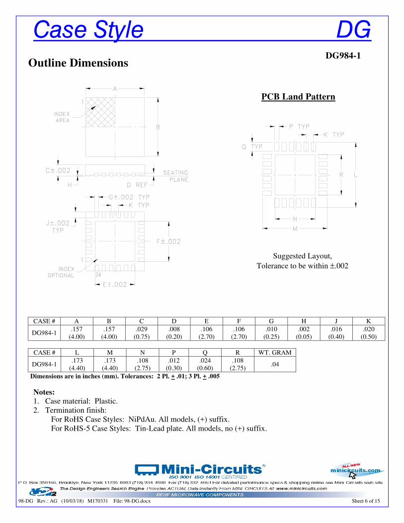
CASE # A B C D E F G H J K
DG984-1 .157
(4.00)
.157
(4.00)
.029
(0.75)
.008
(0.20)
.106
(2.70)
.106
(2.70)
.010
(0.25)
.002
(0.05)
.016
(0.40)
.020
(0.50)
CASE # L M N P Q R WT. GRAM
DG984-1 .173
(4.40)
.173
(4.40)
.108
(2.75)
.012
(0.30)
.024
(0.60)
.108
(2.75) .04
Dimensions are in inches (mm). Tolerances: 2 Pl. + .01; 3 Pl. + .005
Notes:
1. Case material: Plastic.
2. Termination finish:
For RoHS Case Styles: NiPdAu. All models, (+) suffix.
For RoHS-5 Case Styles: Tin-Lead plate. All models, no (+) suffix.
Outline Dimensions
DG984-1
Suggested Layout,
Tolerance to be within ±.002
PCB Land Pattern


Mini-Circuits Environmental Specifications
All Mini-Circuits products are manufactured under exacting quality assurance and control standards, and are capable of meeting published specifications after being subjected to any or all of the following physical and environmental test.
Specification Test/Inspection Condition Reference/Spec
ENV84
Operating Temperature -40° to 85° C or -40° to 105° CAmbient Environment
Refer to Individual Model Data Sheet
Storage Temperature -55° to 100° C or -65° to 150° CAmbient Environment
Refer to Individual Model Data Sheet
Temperature Humidity Bias 85°C, 85% RH, 168 hours J-STD-020
Temperature Cycling -65° to +150°C, 500 cycles MIL-STD-883, Method 1010.8 / JESD22-A104
High Temp Storage 150°C, 1000 hours MIL-STD-883, Method 1008.2 / JESD22-A103
Solder Reflow Heat Pb-Free Process: 260°C peak J-STD-020, Table 4-1, 4-2 and 5-2; Figure 5-1
Solderability Per Standard MIL-STD-883, Method 2003.9 / JESD22-B102
Marking Resistance to Solvents Laser marked, visual observation Mini-Circuits D4-Q4T0-04
This document and its contents are the property of Mini-Circuits.
Rev:ENV84 OR 08/19/16 File:M157739 ENV84.pdfPage: 1