soc design lab, electronic engineering, national changhua university of education, taiwan, r.o.c 1...
TRANSCRIPT
SoC Design Lab, Electronic Engineering, National Changhua University of Education, Taiwan, R.O.C 1
2009/11/30
Presenter: Pin-Chong Chen
Advisor: Tsung-Che Huang
Low-Cost CLT-Based Random Number Generator
for Communication Test

SoC Design Lab, Electronic Engineering, National Changhua University of Education, Taiwan, R.O.C 2
References
Y.-H. Chou, T.-H. Wu and T.-C. Huang, “Low-Cost CLT-based Random Number Generator for Communication Test,”VLSI Test Technology Workshop (VTTW), Test Applications, pp.79-82, Taiwan, Jul. 2009.

SoC Design Lab, Electronic Engineering, National Changhua University of Education, Taiwan, R.O.C 3
Outline
Introduction Previous Work Random Number Generator (RNG)
Normal Distribution RNG Uniform Distribution RNG
Programmable Delay Line (PDL) Coarse-tuned PDL Fine-tuned PDL
Experiment Results Conclusions

SoC Design Lab, Electronic Engineering, National Changhua University of Education, Taiwan, R.O.C 4
Introduction
In high-speed computer and communication systems, timing jitter is one of the most critical parameters.
Jitter testing is becoming indispensable.
Conventional Jitter Generator is executed by expensive external testers or instruments.
This paper develop a CLT-based Random Number Generator for Communication test.

SoC Design Lab, Electronic Engineering, National Changhua University of Education, Taiwan, R.O.C 5
Ideal and Jitter Waveform
Waveform transition is too early
Waveform transition is too lateIdeal Waveform
Jitter is defined as the short-term variations of a digital signal’s significant instants from their ideal positions in time.
Fig. 1 Jitter Waveforms

SoC Design Lab, Electronic Engineering, National Changhua University of Education, Taiwan, R.O.C 6
RNG (Screening Sampling)
)2cos(ln2 21 1 X
)2sin(ln2 22 1 X
Box-Muller
Ziggurat Algorithm
Fig. 2 Typical Ziggurat Algorithm
(1)

SoC Design Lab, Electronic Engineering, National Changhua University of Education, Taiwan, R.O.C 7
RNG (Direct Sampling)
Table LookUp
u n ifo rm d is tr ib u tio n
c d f -1
x
x
z
p d f
norm
al d
istri
butio
n
u n ifo rm d is tr ib u tio n
c d f -1
x
x
z
p d f
sinu
soid
al d
istri
butio
n
(b )(a )
Fig. 3 Typical Table LookUp Methods

SoC Design Lab, Electronic Engineering, National Changhua University of Education, Taiwan, R.O.C 8
Conventional CLT-based RNG
Fig. 4 A Conventional CLT-based RNG
The conventional CLT approves the sum of m independent random variables with uniform distribution, it will be approaching to a normal distribution.

SoC Design Lab, Electronic Engineering, National Changhua University of Education, Taiwan, R.O.C 9
Proposed CLT-based RNG
Fig. 5 Proposed CLT-based RNG
kn
n
n
43
12/
2/
Where k is a non-negative integer

SoC Design Lab, Electronic Engineering, National Changhua University of Education, Taiwan, R.O.C 10
LFSR-based Uniform Distribution RNG/JG
R3 R2 R1 R0Rn
Q[0]Q[1]Q[2]Q[3]Q[n-1]
clk
Exclusive-OR Feedback Circuit
Fig. 6 Uniform Distribution RNG
Q D
k2
in
Q D
Q Q
out
iDiQ
buffers k2
Fig. 7 Uniform Distribution Jitter Generator

SoC Design Lab, Electronic Engineering, National Changhua University of Education, Taiwan, R.O.C 11
CPDL
Q D Q D Q D Q D
02 12 12m m2
Jitter Distribution Control Block
IN OUT
Fig. 8 Coarse-tuned Programmable Delay Line
The jitter distribution control block can include several XOR gates for a uniform distribution RNG or be normal distribution RNG.

SoC Design Lab, Electronic Engineering, National Changhua University of Education, Taiwan, R.O.C 12
FPDL
in out
M[0] M[1] M[2] M[3]
M[0] M[1] M[2] M[3]
Fig. 9 Fine-tuned Programmable Delay Line
SoC Design Lab, Electronic Engineering, National Changhua University of Education, Taiwan, R.O.C 13
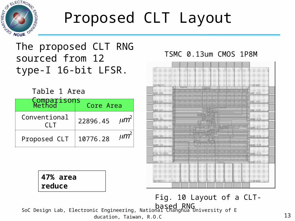
Proposed CLT Layout
Fig. 10 Layout of a CLT-based RNG
TSMC 0.13um CMOS 1P8MThe proposed CLT RNG sourced from 12 type-I 16-bit LFSR.
Method Core Area
Conventional CLT 22896.45
Proposed CLT 10776.28
2m2m
47% area reduce
Table 1 Area Comparisons

SoC Design Lab, Electronic Engineering, National Changhua University of Education, Taiwan, R.O.C 14
Randomness: Scatter Diagram
Fig. 11 Scatter diagrams with 10,000 entries of 16-bit outputs

SoC Design Lab, Electronic Engineering, National Changhua University of Education, Taiwan, R.O.C 15
Goodness of Fit
Fig. 12 Fitting Sampled Number to a Normal Distribution
In Communication test, the fitness is more critical than the randomness.
B
i i
ii
E
EA
1
22 )(
(2)
SoC Design Lab, Electronic Engineering, National Changhua University of Education, Taiwan, R.O.C 16
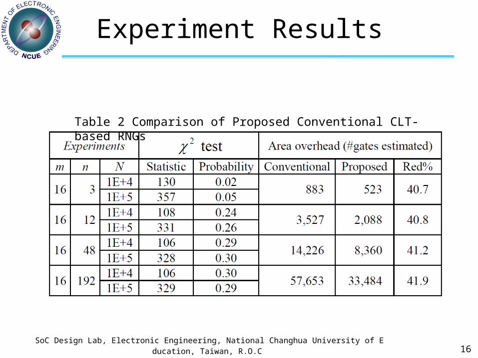
Experiment Results
Table 2 Comparison of Proposed Conventional CLT-based RNGs

SoC Design Lab, Electronic Engineering, National Changhua University of Education, Taiwan, R.O.C 17
Conclusions
In this paper we proposed a theorem to reduce the parallel counter in conventional type-I LFSR-sourced CLT-based RNG to a parallel 1’s counter.
More than 93% of counter area can be saved mainly due to the reduced register length for a 16-bit fraction system.
About 47% of area and 30% of adder levels, namely the propagation time can be reduced.
We proposed a jitter generator embedded in network
on-a-chip or system-in-a-package for communication
test.

SoC Design Lab, Electronic Engineering, National Changhua University of Education, Taiwan, R.O.C 18
Thanks for your attention.