snosbt0l–february 2000–revised … · 4 lm340, lm340a, lm7805, lm7812, lm7815...
TRANSCRIPT
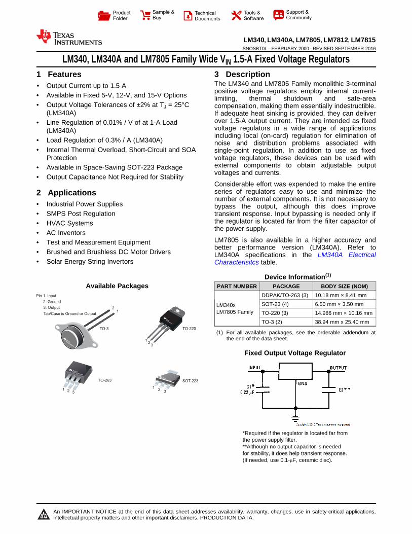
Pin 1. Input
2. Ground
3. Output
Tab/Case is Ground or Output
13
3
1
TO-3
SOT-223
TO-220
TO-263
2
122 3
12
Product
Folder
Sample &Buy
Technical
Documents
Tools &
Software
Support &Community
An IMPORTANT NOTICE at the end of this data sheet addresses availability, warranty, changes, use in safety-critical applications,intellectual property matters and other important disclaimers. PRODUCTION DATA.
LM340, LM340A, LM7805, LM7812, LM7815SNOSBT0L –FEBRUARY 2000–REVISED SEPTEMBER 2016
LM340, LM340A and LM7805 Family Wide VIN 1.5-A Fixed Voltage Regulators
1
1 Features1• Output Current up to 1.5 A• Available in Fixed 5-V, 12-V, and 15-V Options• Output Voltage Tolerances of ±2% at TJ = 25°C
(LM340A)• Line Regulation of 0.01% / V of at 1-A Load
(LM340A)• Load Regulation of 0.3% / A (LM340A)• Internal Thermal Overload, Short-Circuit and SOA
Protection• Available in Space-Saving SOT-223 Package• Output Capacitance Not Required for Stability
2 Applications• Industrial Power Supplies• SMPS Post Regulation• HVAC Systems• AC Inventors• Test and Measurement Equipment• Brushed and Brushless DC Motor Drivers• Solar Energy String Invertors
SPACE
Available Packages
3 DescriptionThe LM340 and LM7805 Family monolithic 3-terminalpositive voltage regulators employ internal current-limiting, thermal shutdown and safe-areacompensation, making them essentially indestructible.If adequate heat sinking is provided, they can deliverover 1.5-A output current. They are intended as fixedvoltage regulators in a wide range of applicationsincluding local (on-card) regulation for elimination ofnoise and distribution problems associated withsingle-point regulation. In addition to use as fixedvoltage regulators, these devices can be used withexternal components to obtain adjustable outputvoltages and currents.
Considerable effort was expended to make the entireseries of regulators easy to use and minimize thenumber of external components. It is not necessary tobypass the output, although this does improvetransient response. Input bypassing is needed only ifthe regulator is located far from the filter capacitor ofthe power supply.
LM7805 is also available in a higher accuracy andbetter performance version (LM340A). Refer toLM340A specifications in the LM340A ElectricalCharacterisitcs table.
Device Information(1)
PART NUMBER PACKAGE BODY SIZE (NOM)
LM340xLM7805 Family
DDPAK/TO-263 (3) 10.18 mm × 8.41 mmSOT-23 (4) 6.50 mm × 3.50 mmTO-220 (3) 14.986 mm × 10.16 mmTO-3 (2) 38.94 mm x 25.40 mm
(1) For all available packages, see the orderable addendum atthe end of the data sheet.
Fixed Output Voltage Regulator
*Required if the regulator is located far fromthe power supply filter.**Although no output capacitor is neededfor stability, it does help transient response.(If needed, use 0.1-μF, ceramic disc).
2
LM340, LM340A, LM7805, LM7812, LM7815SNOSBT0L –FEBRUARY 2000–REVISED SEPTEMBER 2016 www.ti.com
Product Folder Links: LM340 LM340A LM7805 LM7812 LM7815
Submit Documentation Feedback Copyright © 2000–2016, Texas Instruments Incorporated
Table of Contents1 Features .................................................................. 12 Applications ........................................................... 13 Description ............................................................. 14 Revision History..................................................... 25 Pin Configuration and Functions ......................... 36 Specifications......................................................... 4
6.1 Absolute Maximum Ratings ...................................... 46.2 ESD Ratings.............................................................. 46.3 Recommended Operating Conditions....................... 46.4 Thermal Information .................................................. 46.5 LM340A Electrical Characteristics,VO = 5 V, VI = 10 V............................................................ 56.6 LM340 / LM7805 Electrical Characteristics,VO = 5 V, VI = 10 V............................................................ 66.7 LM340 / LM7812 Electrical Characteristics,VO = 12 V, VI = 19 V.......................................................... 76.8 LM340 / LM7815 Electrical Characteristics,VO = 15 V, VI = 23 V.......................................................... 86.9 Typical Characteristics .............................................. 9
7 Detailed Description ............................................ 127.1 Overview ................................................................. 127.2 Functional Block Diagram ....................................... 12
7.3 Feature Description................................................. 127.4 Device Functional Modes........................................ 12
8 Application and Implementation ........................ 138.1 Application Information............................................ 138.2 Typical Applications ................................................ 148.3 System Examples ................................................... 15
9 Power Supply Recommendations ...................... 1710 Layout................................................................... 17
10.1 Layout Guidelines ................................................. 1710.2 Layout Example ................................................... 1710.3 Heat Sinking DDPAK/TO-263 and SOT-223
Package Parts.......................................................... 1811 Device and Documentation Support ................. 20
11.1 Documentation Support ........................................ 2011.2 Related Links ........................................................ 2011.3 Receiving Notification of Documentation Updates 2011.4 Community Resources.......................................... 2011.5 Trademarks ........................................................... 2011.6 Electrostatic Discharge Caution............................ 2011.7 Glossary ................................................................ 20
12 Mechanical, Packaging, and OrderableInformation ........................................................... 21
4 Revision HistoryNOTE: Page numbers for previous revisions may differ from page numbers in the current version.
Changes from Revision K (November 2015) to Revision L Page
• Changed pinout number order for the TO-220 and SOT-223 packages from: 2, 3, 1 to: 1, 2, 3 .......................................... 1
Changes from Revision J (December 2013) to Revision K Page
• Added ESD Ratings table, Thermal Information table, Feature Description section, Device Functional Modes,Application and Implementation section, Power Supply Recommendations section, Layout section, Device andDocumentation Support section, and Mechanical, Packaging, and Orderable Information section....................................... 1
• Deleted obsolete LM140 and LM7808C devices from the data sheet ................................................................................... 1• Changed Figure 13 caption from Line Regulation 140AK-5.0 to Line Regulation LM340, .................................................. 11• Changed Figure 14 caption from Line Regulation 140AK-5.0 to Line Regulation LM340, .................................................. 11
Changes from Revision I (March 2013) to Revision J Page
• Changed 0.5 from typ to max ................................................................................................................................................. 5
3
LM340, LM340A, LM7805, LM7812, LM7815www.ti.com SNOSBT0L –FEBRUARY 2000–REVISED SEPTEMBER 2016
Product Folder Links: LM340 LM340A LM7805 LM7812 LM7815
Submit Documentation FeedbackCopyright © 2000–2016, Texas Instruments Incorporated
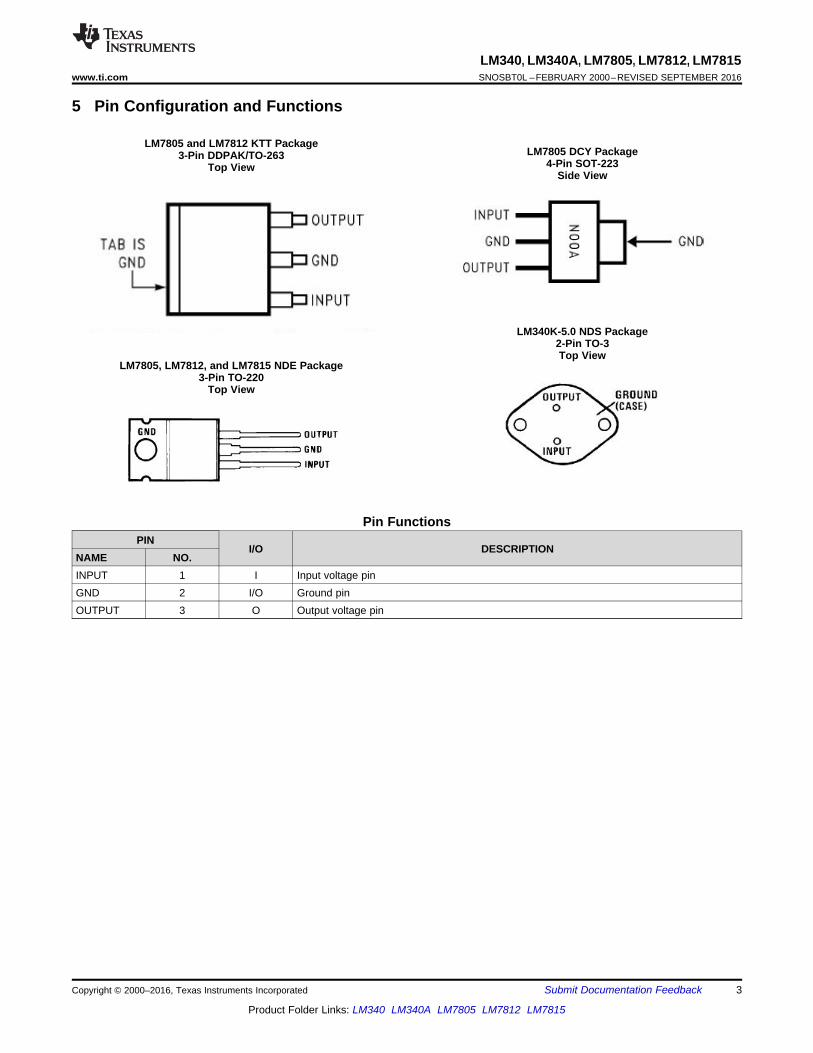
5 Pin Configuration and Functions
LM7805 and LM7812 KTT Package3-Pin DDPAK/TO-263
Top View
LM7805, LM7812, and LM7815 NDE Package3-Pin TO-220
Top View
LM7805 DCY Package4-Pin SOT-223
Side View
LM340K-5.0 NDS Package2-Pin TO-3Top View
Pin FunctionsPIN
I/O DESCRIPTIONNAME NO.INPUT 1 I Input voltage pinGND 2 I/O Ground pinOUTPUT 3 O Output voltage pin
4
LM340, LM340A, LM7805, LM7812, LM7815SNOSBT0L –FEBRUARY 2000–REVISED SEPTEMBER 2016 www.ti.com
Product Folder Links: LM340 LM340A LM7805 LM7812 LM7815
Submit Documentation Feedback Copyright © 2000–2016, Texas Instruments Incorporated
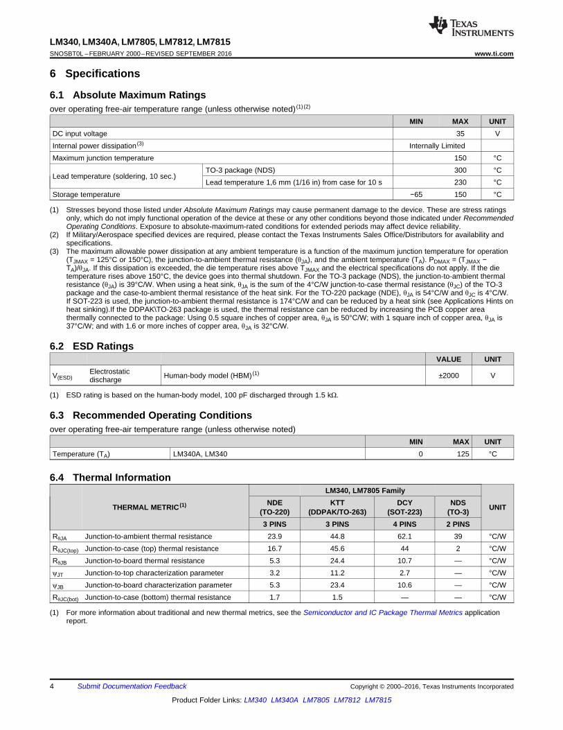
(1) Stresses beyond those listed under Absolute Maximum Ratings may cause permanent damage to the device. These are stress ratingsonly, which do not imply functional operation of the device at these or any other conditions beyond those indicated under RecommendedOperating Conditions. Exposure to absolute-maximum-rated conditions for extended periods may affect device reliability.
(2) If Military/Aerospace specified devices are required, please contact the Texas Instruments Sales Office/Distributors for availability andspecifications.
(3) The maximum allowable power dissipation at any ambient temperature is a function of the maximum junction temperature for operation(TJMAX = 125°C or 150°C), the junction-to-ambient thermal resistance (θJA), and the ambient temperature (TA). PDMAX = (TJMAX −TA)/θJA. If this dissipation is exceeded, the die temperature rises above TJMAX and the electrical specifications do not apply. If the dietemperature rises above 150°C, the device goes into thermal shutdown. For the TO-3 package (NDS), the junction-to-ambient thermalresistance (θJA) is 39°C/W. When using a heat sink, θJA is the sum of the 4°C/W junction-to-case thermal resistance (θJC) of the TO-3package and the case-to-ambient thermal resistance of the heat sink. For the TO-220 package (NDE), θJA is 54°C/W and θJC is 4°C/W.If SOT-223 is used, the junction-to-ambient thermal resistance is 174°C/W and can be reduced by a heat sink (see Applications Hints onheat sinking).If the DDPAK\TO-263 package is used, the thermal resistance can be reduced by increasing the PCB copper areathermally connected to the package: Using 0.5 square inches of copper area, θJA is 50°C/W; with 1 square inch of copper area, θJA is37°C/W; and with 1.6 or more inches of copper area, θJA is 32°C/W.
6 Specifications
6.1 Absolute Maximum Ratingsover operating free-air temperature range (unless otherwise noted) (1) (2)
MIN MAX UNITDC input voltage 35 VInternal power dissipation (3) Internally LimitedMaximum junction temperature 150 °C
Lead temperature (soldering, 10 sec.)TO-3 package (NDS) 300 °CLead temperature 1,6 mm (1/16 in) from case for 10 s 230 °C
Storage temperature −65 150 °C
(1) ESD rating is based on the human-body model, 100 pF discharged through 1.5 kΩ.
6.2 ESD RatingsVALUE UNIT
V(ESD)Electrostaticdischarge Human-body model (HBM) (1) ±2000 V
6.3 Recommended Operating Conditionsover operating free-air temperature range (unless otherwise noted)
MIN MAX UNITTemperature (TA) LM340A, LM340 0 125 °C
(1) For more information about traditional and new thermal metrics, see the Semiconductor and IC Package Thermal Metrics applicationreport.
6.4 Thermal Information
THERMAL METRIC (1)
LM340, LM7805 Family
UNITNDE(TO-220)
KTT(DDPAK/TO-263)
DCY(SOT-223)
NDS(TO-3)
3 PINS 3 PINS 4 PINS 2 PINSRθJA Junction-to-ambient thermal resistance 23.9 44.8 62.1 39 °C/WRθJC(top) Junction-to-case (top) thermal resistance 16.7 45.6 44 2 °C/WRθJB Junction-to-board thermal resistance 5.3 24.4 10.7 — °C/WψJT Junction-to-top characterization parameter 3.2 11.2 2.7 — °C/WψJB Junction-to-board characterization parameter 5.3 23.4 10.6 — °C/WRθJC(bot) Junction-to-case (bottom) thermal resistance 1.7 1.5 — — °C/W
5
LM340, LM340A, LM7805, LM7812, LM7815www.ti.com SNOSBT0L –FEBRUARY 2000–REVISED SEPTEMBER 2016
Product Folder Links: LM340 LM340A LM7805 LM7812 LM7815
Submit Documentation FeedbackCopyright © 2000–2016, Texas Instruments Incorporated
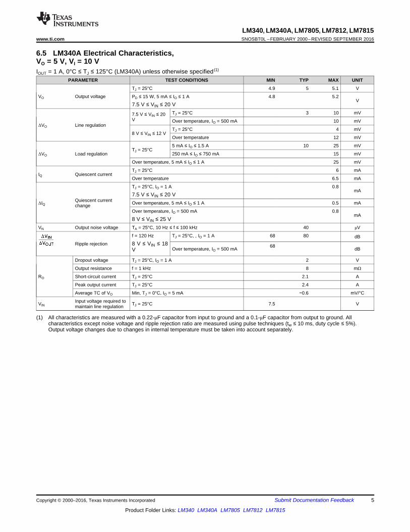
(1) All characteristics are measured with a 0.22-μF capacitor from input to ground and a 0.1-μF capacitor from output to ground. Allcharacteristics except noise voltage and ripple rejection ratio are measured using pulse techniques (tw ≤ 10 ms, duty cycle ≤ 5%).Output voltage changes due to changes in internal temperature must be taken into account separately.
6.5 LM340A Electrical Characteristics,VO = 5 V, VI = 10 VIOUT = 1 A, 0°C ≤ TJ ≤ 125°C (LM340A) unless otherwise specified (1)
PARAMETER TEST CONDITIONS MIN TYP MAX UNIT
VO Output voltage
TJ = 25°C 4.9 5 5.1 V
PD ≤ 15 W, 5 mA ≤ IO ≤ 1 A
7.5 V ≤ VIN ≤ 20 V4.8 5.2
V
ΔVO Line regulation
7.5 V ≤ VIN ≤ 20V
TJ = 25°C 3 10 mV
Over temperature, IO = 500 mA 10 mV
8 V ≤ VIN ≤ 12 VTJ = 25°C 4 mV
Over temperature 12 mV
ΔVO Load regulationTJ = 25°C
5 mA ≤ IO ≤ 1.5 A 10 25 mV
250 mA ≤ IO ≤ 750 mA 15 mV
Over temperature, 5 mA ≤ IO ≤ 1 A 25 mV
IQ Quiescent currentTJ = 25°C 6 mA
Over temperature 6.5 mA
ΔIQQuiescent currentchange
TJ = 25°C, IO = 1 A
7.5 V ≤ VIN ≤ 20 V0.8
mA
Over temperature, 5 mA ≤ IO ≤ 1 A 0.5 mA
Over temperature, IO = 500 mA
8 V ≤ VIN ≤ 25 V0.8
mA
VN Output noise voltage TA = 25°C, 10 Hz ≤ f ≤ 100 kHz 40 μV
Ripple rejection
f = 120 Hz
8 V ≤ VIN ≤ 18V
TJ = 25°C, , IO = 1 A 68 80 dB
Over temperature, IO = 500 mA 68 dB
RO
Dropout voltage TJ = 25°C, IO = 1 A 2 V
Output resistance f = 1 kHz 8 mΩ
Short-circuit current TJ = 25°C 2.1 A
Peak output current TJ = 25°C 2.4 A
Average TC of VO Min, TJ = 0°C, IO = 5 mA −0.6 mV/°C
VINInput voltage required tomaintain line regulation TJ = 25°C 7.5 V
6
LM340, LM340A, LM7805, LM7812, LM7815SNOSBT0L –FEBRUARY 2000–REVISED SEPTEMBER 2016 www.ti.com
Product Folder Links: LM340 LM340A LM7805 LM7812 LM7815
Submit Documentation Feedback Copyright © 2000–2016, Texas Instruments Incorporated
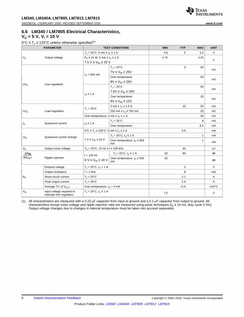
(1) All characteristics are measured with a 0.22-μF capacitor from input to ground and a 0.1-μF capacitor from output to ground. Allcharacteristics except noise voltage and ripple rejection ratio are measured using pulse techniques (tw ≤ 10 ms, duty cycle ≤ 5%).Output voltage changes due to changes in internal temperature must be taken into account separately.
6.6 LM340 / LM7805 Electrical Characteristics,VO = 5 V, VI = 10 V0°C ≤ TJ ≤ 125°C unless otherwise specified (1)
PARAMETER TEST CONDITIONS MIN TYP MAX UNIT
VO Output voltage
TJ = 25°C, 5 mA ≤ IO ≤ 1 A 4.8 5 5.2 V
PD ≤ 15 W, 5 mA ≤ IO ≤ 1 A
7.5 V ≤ VIN ≤ 20 V4.75 5.25
V
ΔVO Line regulation
IO = 500 mA
TJ = 25°C
7V ≤ VIN ≤ 25V3 50
mV
Over temperature
8V ≤ VIN ≤ 20V50
mV
IO ≤ 1 A
TJ = 25°C
7.5V ≤ VIN ≤ 20V50
mV
Over temperature
8V ≤ VIN ≤ 12V25
mV
ΔVO Load regulationTJ = 25°C
5 mA ≤ IO ≤ 1.5 A 10 50 mV
250 mA ≤ IO ≤ 750 mA 25 mV
Over temperature, 5 mA ≤ IO ≤ 1 A 50 mV
IQ Quiescent current IO ≤ 1 ATJ = 25°C 8 mA
Over temperature 8.5 mA
ΔIQ Quiescent current change
0°C ≤ TJ ≤ 125°C, 5 mA ≤ IO ≤ 1 A 0.5 mA
7 V ≤ VIN ≤ 20 VTJ = 25°C, IO ≤ 1 A 1 mA
Over temperature, IO ≤ 500mA
1 mA
VN Output noise voltage TA = 25°C, 10 Hz ≤ f ≤ 100 kHz 40 μV
Ripple rejectionf = 120 Hz
8 V ≤ VIN ≤ 18 V
TJ = 25°C, IO ≤ 1 A 62 80 dB
Over temperature, IO ≤ 500mA
62dB
RO
Dropout voltage TJ = 25°C, IO = 1 A 2 V
Output resistance f = 1 kHz 8 mΩ
Short-circuit current TJ = 25°C 2.1 A
Peak output current TJ = 25°C 2.4 A
Average TC of VOUT Over temperature, IO = 5 mA −0.6 mV/°C
VIN Input voltage required tomaintain line regulation
TJ = 25°C, IO ≤ 1 A 7.5 V
7
LM340, LM340A, LM7805, LM7812, LM7815www.ti.com SNOSBT0L –FEBRUARY 2000–REVISED SEPTEMBER 2016
Product Folder Links: LM340 LM340A LM7805 LM7812 LM7815
Submit Documentation FeedbackCopyright © 2000–2016, Texas Instruments Incorporated
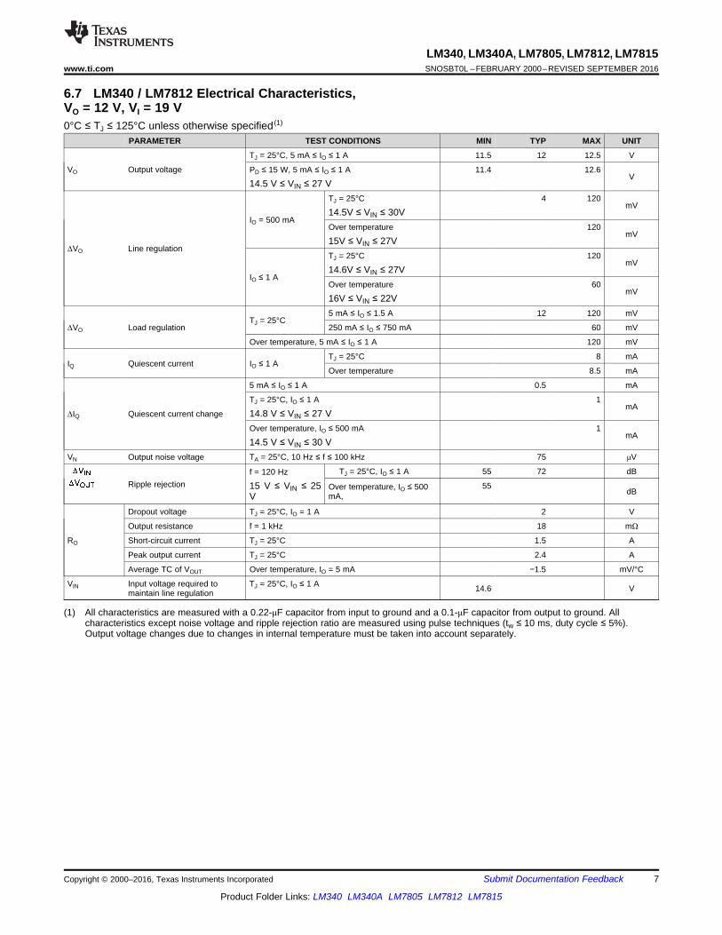
(1) All characteristics are measured with a 0.22-μF capacitor from input to ground and a 0.1-μF capacitor from output to ground. Allcharacteristics except noise voltage and ripple rejection ratio are measured using pulse techniques (tw ≤ 10 ms, duty cycle ≤ 5%).Output voltage changes due to changes in internal temperature must be taken into account separately.
6.7 LM340 / LM7812 Electrical Characteristics,VO = 12 V, VI = 19 V0°C ≤ TJ ≤ 125°C unless otherwise specified (1)
PARAMETER TEST CONDITIONS MIN TYP MAX UNIT
VO Output voltage
TJ = 25°C, 5 mA ≤ IO ≤ 1 A 11.5 12 12.5 V
PD ≤ 15 W, 5 mA ≤ IO ≤ 1 A
14.5 V ≤ VIN ≤ 27 V11.4 12.6
V
ΔVO Line regulation
IO = 500 mA
TJ = 25°C
14.5V ≤ VIN ≤ 30V4 120
mV
Over temperature
15V ≤ VIN ≤ 27V120
mV
IO ≤ 1 A
TJ = 25°C
14.6V ≤ VIN ≤ 27V120
mV
Over temperature
16V ≤ VIN ≤ 22V60
mV
ΔVO Load regulationTJ = 25°C
5 mA ≤ IO ≤ 1.5 A 12 120 mV
250 mA ≤ IO ≤ 750 mA 60 mV
Over temperature, 5 mA ≤ IO ≤ 1 A 120 mV
IQ Quiescent current IO ≤ 1 ATJ = 25°C 8 mA
Over temperature 8.5 mA
ΔIQ Quiescent current change
5 mA ≤ IO ≤ 1 A 0.5 mA
TJ = 25°C, IO ≤ 1 A
14.8 V ≤ VIN ≤ 27 V1
mA
Over temperature, IO ≤ 500 mA
14.5 V ≤ VIN ≤ 30 V1
mA
VN Output noise voltage TA = 25°C, 10 Hz ≤ f ≤ 100 kHz 75 μV
Ripple rejectionf = 120 Hz
15 V ≤ VIN ≤ 25V
TJ = 25°C, IO ≤ 1 A 55 72 dB
Over temperature, IO ≤ 500mA,
55dB
RO
Dropout voltage TJ = 25°C, IO = 1 A 2 V
Output resistance f = 1 kHz 18 mΩ
Short-circuit current TJ = 25°C 1.5 A
Peak output current TJ = 25°C 2.4 A
Average TC of VOUT Over temperature, IO = 5 mA −1.5 mV/°C
VIN Input voltage required tomaintain line regulation
TJ = 25°C, IO ≤ 1 A 14.6 V
8
LM340, LM340A, LM7805, LM7812, LM7815SNOSBT0L –FEBRUARY 2000–REVISED SEPTEMBER 2016 www.ti.com
Product Folder Links: LM340 LM340A LM7805 LM7812 LM7815
Submit Documentation Feedback Copyright © 2000–2016, Texas Instruments Incorporated
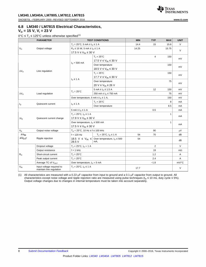
(1) All characteristics are measured with a 0.22-μF capacitor from input to ground and a 0.1-μF capacitor from output to ground. Allcharacteristics except noise voltage and ripple rejection ratio are measured using pulse techniques (tw ≤ 10 ms, duty cycle ≤ 5%).Output voltage changes due to changes in internal temperature must be taken into account separately.
6.8 LM340 / LM7815 Electrical Characteristics,VO = 15 V, VI = 23 V0°C ≤ TJ ≤ 125°C unless otherwise specified (1)
PARAMETER TEST CONDITIONS MIN TYP MAX UNIT
VO Output voltage
TJ = 25°C, 5 mA ≤ IO ≤ 1 A 14.4 15 15.6 V
PD ≤ 15 W, 5 mA ≤ IO ≤ 1 A
17.5 V ≤ VIN ≤ 30 V14.25 15.75
V
ΔVO Line regulation
IO = 500 mA
TJ = 25°C
17.5 V ≤ VIN ≤ 30 V4 150
mV
Over temperature
18.5 V ≤ VIN ≤ 30 V150
mV
IO ≤ 1 A
TJ = 25°C
17.7 V ≤ VIN ≤ 30 V150
mV
Over temperature
20 V ≤ VIN ≤ 26 V75
mV
ΔVO Load regulationTJ = 25°C
5 mA ≤ IO ≤ 1.5 A 12 150 mV
250 mA ≤ IO ≤ 750 mA 75 mV
Over temperature, 5 mA ≤ IO ≤ 1 A, 150 mV
IQ Quiescent current IO ≤ 1 ATJ = 25°C 8 mA
Over temperature 8.5 mA
ΔIQ Quiescent current change
5 mA ≤ IO ≤ 1 A 0.5 mA
TJ = 25°C, IO ≤ 1 A
17.9 V ≤ VIN ≤ 30 V1
mA
Over temperature, IO ≤ 500 mA
17.5 V ≤ VIN ≤ 30 V1
mA
VN Output noise voltage TA = 25°C, 10 Hz ≤ f ≤ 100 kHz 90 μV
Ripple rejectionf = 120 Hz
18.5 V ≤ VIN ≤28.5 V
TJ = 25°C, IO ≤ 1 A 54 70 dB
Over temperature, IO ≤ 500mA,
54dB
RO
Dropout voltage TJ = 25°C, IO = 1 A 2 V
Output resistance f = 1 kHz 19 mΩ
Short-circuit current TJ = 25°C 1.2 A
Peak output current TJ = 25°C 2.4 A
Average TC of VOUT Over temperature, IO = 5 mA −1.8 mV/°C
VIN Input voltage required tomaintain line regulation
TJ = 25°C, IO ≤ 1 A 17.7 V
9
LM340, LM340A, LM7805, LM7812, LM7815www.ti.com SNOSBT0L –FEBRUARY 2000–REVISED SEPTEMBER 2016
Product Folder Links: LM340 LM340A LM7805 LM7812 LM7815
Submit Documentation FeedbackCopyright © 2000–2016, Texas Instruments Incorporated
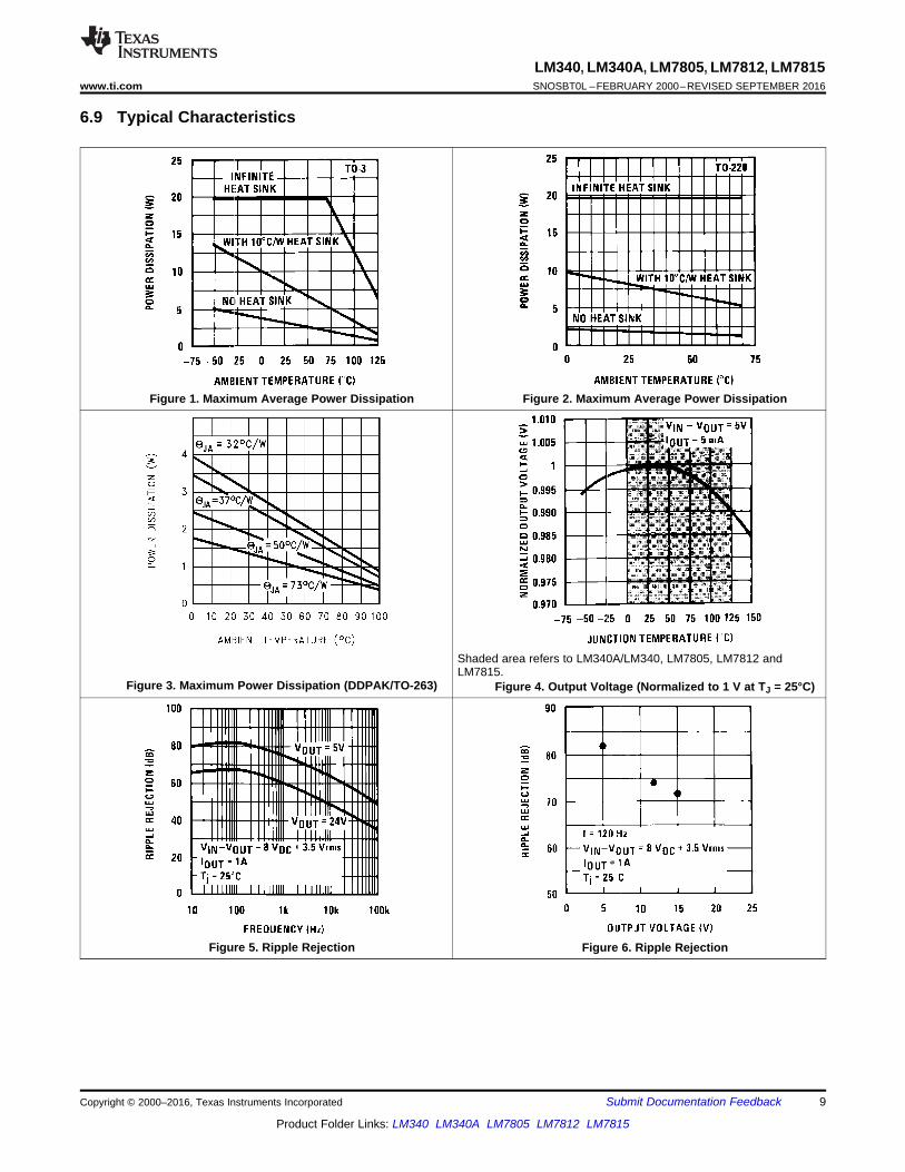
6.9 Typical Characteristics
Figure 1. Maximum Average Power Dissipation Figure 2. Maximum Average Power Dissipation
Figure 3. Maximum Power Dissipation (DDPAK/TO-263)
Shaded area refers to LM340A/LM340, LM7805, LM7812 andLM7815.
Figure 4. Output Voltage (Normalized to 1 V at TJ = 25°C)
Figure 5. Ripple Rejection Figure 6. Ripple Rejection
10
LM340, LM340A, LM7805, LM7812, LM7815SNOSBT0L –FEBRUARY 2000–REVISED SEPTEMBER 2016 www.ti.com
Product Folder Links: LM340 LM340A LM7805 LM7812 LM7815
Submit Documentation Feedback Copyright © 2000–2016, Texas Instruments Incorporated
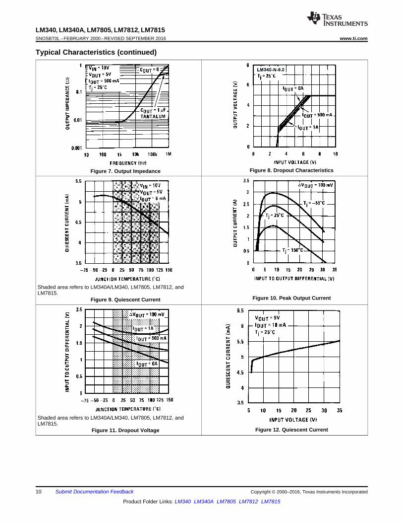
Typical Characteristics (continued)
Figure 7. Output Impedance Figure 8. Dropout Characteristics
Shaded area refers to LM340A/LM340, LM7805, LM7812, andLM7815.
Figure 9. Quiescent Current Figure 10. Peak Output Current
Shaded area refers to LM340A/LM340, LM7805, LM7812, andLM7815.
Figure 11. Dropout Voltage Figure 12. Quiescent Current
11
LM340, LM340A, LM7805, LM7812, LM7815www.ti.com SNOSBT0L –FEBRUARY 2000–REVISED SEPTEMBER 2016
Product Folder Links: LM340 LM340A LM7805 LM7812 LM7815
Submit Documentation FeedbackCopyright © 2000–2016, Texas Instruments Incorporated
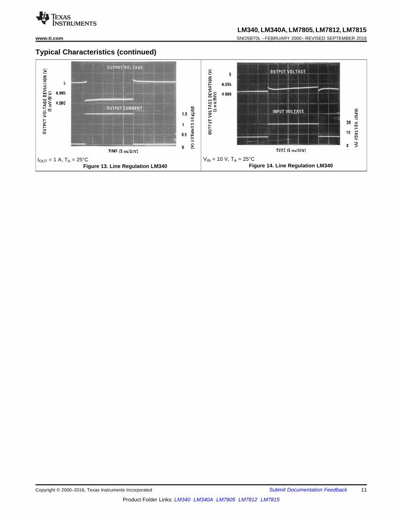
Typical Characteristics (continued)
IOUT = 1 A, TA = 25°CFigure 13. Line Regulation LM340
VIN = 10 V, TA = 25°CFigure 14. Line Regulation LM340
12
LM340, LM340A, LM7805, LM7812, LM7815SNOSBT0L –FEBRUARY 2000–REVISED SEPTEMBER 2016 www.ti.com
Product Folder Links: LM340 LM340A LM7805 LM7812 LM7815
Submit Documentation Feedback Copyright © 2000–2016, Texas Instruments Incorporated
7 Detailed Description
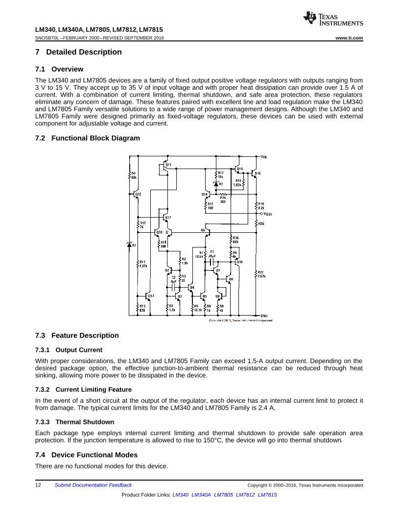
7.1 OverviewThe LM340 and LM7805 devices are a family of fixed output positive voltage regulators with outputs ranging from3 V to 15 V. They accept up to 35 V of input voltage and with proper heat dissipation can provide over 1.5 A ofcurrent. With a combination of current limiting, thermal shutdown, and safe area protection, these regulatorseliminate any concern of damage. These features paired with excellent line and load regulation make the LM340and LM7805 Family versatile solutions to a wide range of power management designs. Although the LM340 andLM7805 Family were designed primarily as fixed-voltage regulators, these devices can be used with externalcomponent for adjustable voltage and current.
7.2 Functional Block Diagram
7.3 Feature Description
7.3.1 Output CurrentWith proper considerations, the LM340 and LM7805 Family can exceed 1.5-A output current. Depending on thedesired package option, the effective junction-to-ambient thermal resistance can be reduced through heatsinking, allowing more power to be dissipated in the device.
7.3.2 Current Limiting FeatureIn the event of a short circuit at the output of the regulator, each device has an internal current limit to protect itfrom damage. The typical current limits for the LM340 and LM7805 Family is 2.4 A.
7.3.3 Thermal ShutdownEach package type employs internal current limiting and thermal shutdown to provide safe operation areaprotection. If the junction temperature is allowed to rise to 150°C, the device will go into thermal shutdown.
7.4 Device Functional ModesThere are no functional modes for this device.
13
LM340, LM340A, LM7805, LM7812, LM7815www.ti.com SNOSBT0L –FEBRUARY 2000–REVISED SEPTEMBER 2016
Product Folder Links: LM340 LM340A LM7805 LM7812 LM7815
Submit Documentation FeedbackCopyright © 2000–2016, Texas Instruments Incorporated
8 Application and Implementation
NOTEInformation in the following applications sections is not part of the TI componentspecification, and TI does not warrant its accuracy or completeness. TI’s customers areresponsible for determining suitability of components for their purposes. Customers shouldvalidate and test their design implementation to confirm system functionality.
8.1 Application InformationThe LM340x and LM7805 series is designed with thermal protection, output short-circuit protection, and outputtransistor safe area protection. However, as with any IC regulator, it becomes necessary to take precautions toassure that the regulator is not inadvertently damaged. The following describes possible misapplications andmethods to prevent damage to the regulator.
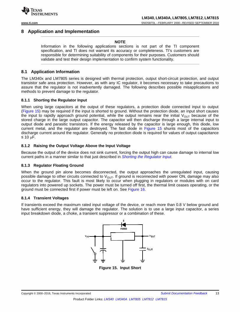
8.1.1 Shorting the Regulator InputWhen using large capacitors at the output of these regulators, a protection diode connected input to output(Figure 15) may be required if the input is shorted to ground. Without the protection diode, an input short causesthe input to rapidly approach ground potential, while the output remains near the initial VOUT because of thestored charge in the large output capacitor. The capacitor will then discharge through a large internal input tooutput diode and parasitic transistors. If the energy released by the capacitor is large enough, this diode, lowcurrent metal, and the regulator are destroyed. The fast diode in Figure 15 shunts most of the capacitorsdischarge current around the regulator. Generally no protection diode is required for values of output capacitance≤ 10 μF.
8.1.2 Raising the Output Voltage Above the Input VoltageBecause the output of the device does not sink current, forcing the output high can cause damage to internal lowcurrent paths in a manner similar to that just described in Shorting the Regulator Input.
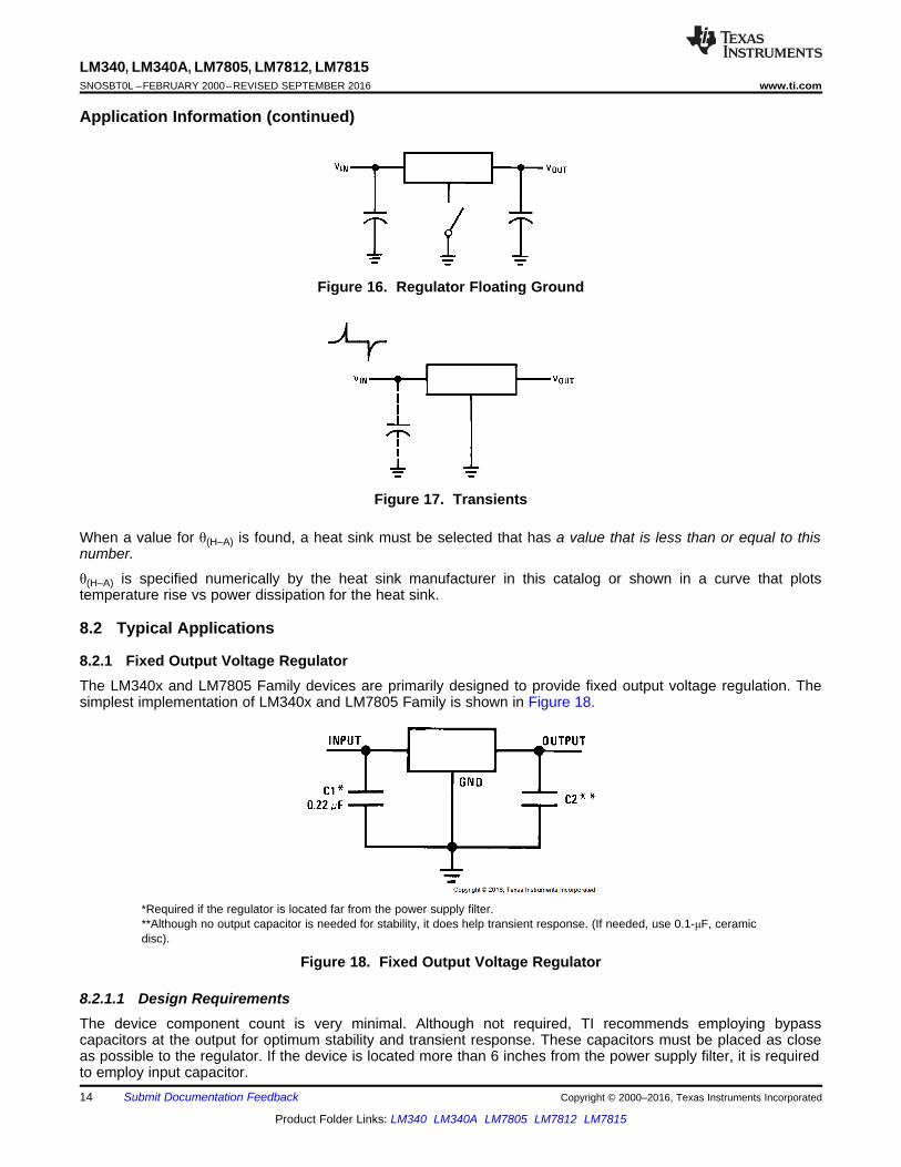
8.1.3 Regulator Floating GroundWhen the ground pin alone becomes disconnected, the output approaches the unregulated input, causingpossible damage to other circuits connected to VOUT. If ground is reconnected with power ON, damage may alsooccur to the regulator. This fault is most likely to occur when plugging in regulators or modules with on cardregulators into powered up sockets. The power must be turned off first, the thermal limit ceases operating, or theground must be connected first if power must be left on. See Figure 16.
8.1.4 Transient VoltagesIf transients exceed the maximum rated input voltage of the device, or reach more than 0.8 V below ground andhave sufficient energy, they will damage the regulator. The solution is to use a large input capacitor, a seriesinput breakdown diode, a choke, a transient suppressor or a combination of these.
Figure 15. Input Short
14
LM340, LM340A, LM7805, LM7812, LM7815SNOSBT0L –FEBRUARY 2000–REVISED SEPTEMBER 2016 www.ti.com
Product Folder Links: LM340 LM340A LM7805 LM7812 LM7815
Submit Documentation Feedback Copyright © 2000–2016, Texas Instruments Incorporated
Application Information (continued)
Figure 16. Regulator Floating Ground
Figure 17. Transients
When a value for θ(H–A) is found, a heat sink must be selected that has a value that is less than or equal to thisnumber.
θ(H–A) is specified numerically by the heat sink manufacturer in this catalog or shown in a curve that plotstemperature rise vs power dissipation for the heat sink.
8.2 Typical Applications
8.2.1 Fixed Output Voltage RegulatorThe LM340x and LM7805 Family devices are primarily designed to provide fixed output voltage regulation. Thesimplest implementation of LM340x and LM7805 Family is shown in Figure 18.
*Required if the regulator is located far from the power supply filter.**Although no output capacitor is needed for stability, it does help transient response. (If needed, use 0.1-μF, ceramicdisc).
Figure 18. Fixed Output Voltage Regulator
8.2.1.1 Design RequirementsThe device component count is very minimal. Although not required, TI recommends employing bypasscapacitors at the output for optimum stability and transient response. These capacitors must be placed as closeas possible to the regulator. If the device is located more than 6 inches from the power supply filter, it is requiredto employ input capacitor.

0.1 PF0.22 PF
OUTPUTINPUT
GND
VOVI
0.1 PF0.22 PF
OUTPUTINPUT
GND
VOVI
15
LM340, LM340A, LM7805, LM7812, LM7815www.ti.com SNOSBT0L –FEBRUARY 2000–REVISED SEPTEMBER 2016
Product Folder Links: LM340 LM340A LM7805 LM7812 LM7815
Submit Documentation FeedbackCopyright © 2000–2016, Texas Instruments Incorporated
Typical Applications (continued)8.2.1.2 Detailed Design ProcedureThe output voltage is set based on the device variant. LM340x and LM7805 Family are available in 5-V, 12-Vand 15-V regulator options.
8.2.1.3 Application Curve
Figure 19. VOUT vs VIN, VOUT = 5 V
8.3 System Examples
IOUT = V2–3 / R1 + IQΔIQ = 1.3 mA over line and load changes.
VOUT = 5 V + (5 V/R1 + IQ) R2 5 V/R1 > 3 IQ,load regulation (Lr) ≈ [(R1 + R2)/R1] (Lr of LM340-5).
Figure 20. Current Regulator Figure 21. Adjustable Output Regulator
Figure 22. High Input Voltage Circuit With SeriesResistor
Figure 23. High Input Voltage Circuitimplementation With Transistor
0.1 PF
OUTPUTINPUT
GND
+ OUT
+ +
0.1 PF
OUTPUTINPUT
GND
- OUT
+ +
LM340
LM79xx
0.1 PF0.22 PF
OUTPUT
INPUT
GND
VO
R13.0:
Q12N6133
IO MAX
IQ1
IREG
VI
0.1 PF0.22 PF
OUTPUT
INPUT
GND
OUT
R13.0:
Q12N6132
IN
RSC
Q22N6124
16
LM340, LM340A, LM7805, LM7812, LM7815SNOSBT0L –FEBRUARY 2000–REVISED SEPTEMBER 2016 www.ti.com
Product Folder Links: LM340 LM340A LM7805 LM7812 LM7815
Submit Documentation Feedback Copyright © 2000–2016, Texas Instruments Incorporated
System Examples (continued)
β(Q1) ≥ IO Max / IREG MaxR1 = 0.9 / IREG = β(Q1) VBE(Q1) / IREG Max (β +1) – IO Max
RSC = 0.8 / ISCR1 = βVBE(Q1) / IREG Max (β +1) – IO Max
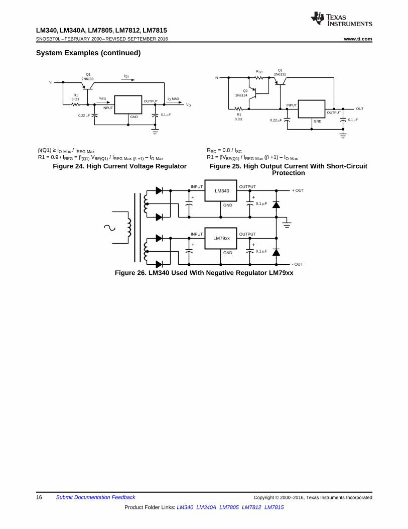
Figure 24. High Current Voltage Regulator Figure 25. High Output Current With Short-CircuitProtection
Figure 26. LM340 Used With Negative Regulator LM79xx
17
LM340, LM340A, LM7805, LM7812, LM7815www.ti.com SNOSBT0L –FEBRUARY 2000–REVISED SEPTEMBER 2016
Product Folder Links: LM340 LM340A LM7805 LM7812 LM7815
Submit Documentation FeedbackCopyright © 2000–2016, Texas Instruments Incorporated
9 Power Supply RecommendationsThe LM340 is designed to operate from a wide input voltage up to 35 V. Please refer to electrical characteristicstables for the minimum input voltage required for line/load regulation. If the device is more than six inches fromthe input filter capacitors, an input bypass capacitor, 0.1 μF or greater, of any type is needed for stability.
10 Layout
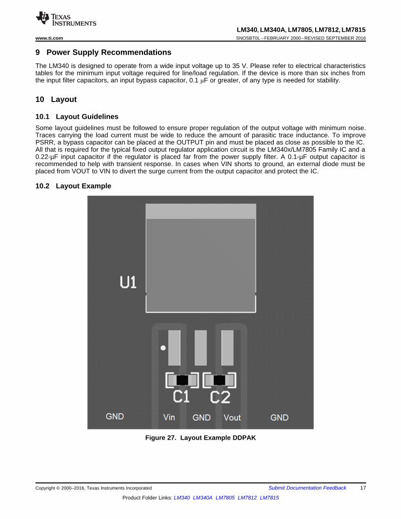
10.1 Layout GuidelinesSome layout guidelines must be followed to ensure proper regulation of the output voltage with minimum noise.Traces carrying the load current must be wide to reduce the amount of parasitic trace inductance. To improvePSRR, a bypass capacitor can be placed at the OUTPUT pin and must be placed as close as possible to the IC.All that is required for the typical fixed output regulator application circuit is the LM340x/LM7805 Family IC and a0.22-µF input capacitor if the regulator is placed far from the power supply filter. A 0.1-µF output capacitor isrecommended to help with transient response. In cases when VIN shorts to ground, an external diode must beplaced from VOUT to VIN to divert the surge current from the output capacitor and protect the IC.
10.2 Layout Example
Figure 27. Layout Example DDPAK
18
LM340, LM340A, LM7805, LM7812, LM7815SNOSBT0L –FEBRUARY 2000–REVISED SEPTEMBER 2016 www.ti.com
Product Folder Links: LM340 LM340A LM7805 LM7812 LM7815
Submit Documentation Feedback Copyright © 2000–2016, Texas Instruments Incorporated
Layout Example (continued)
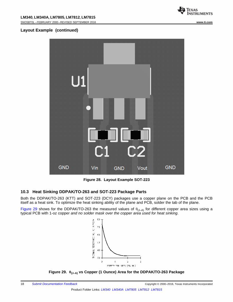
Figure 28. Layout Example SOT-223
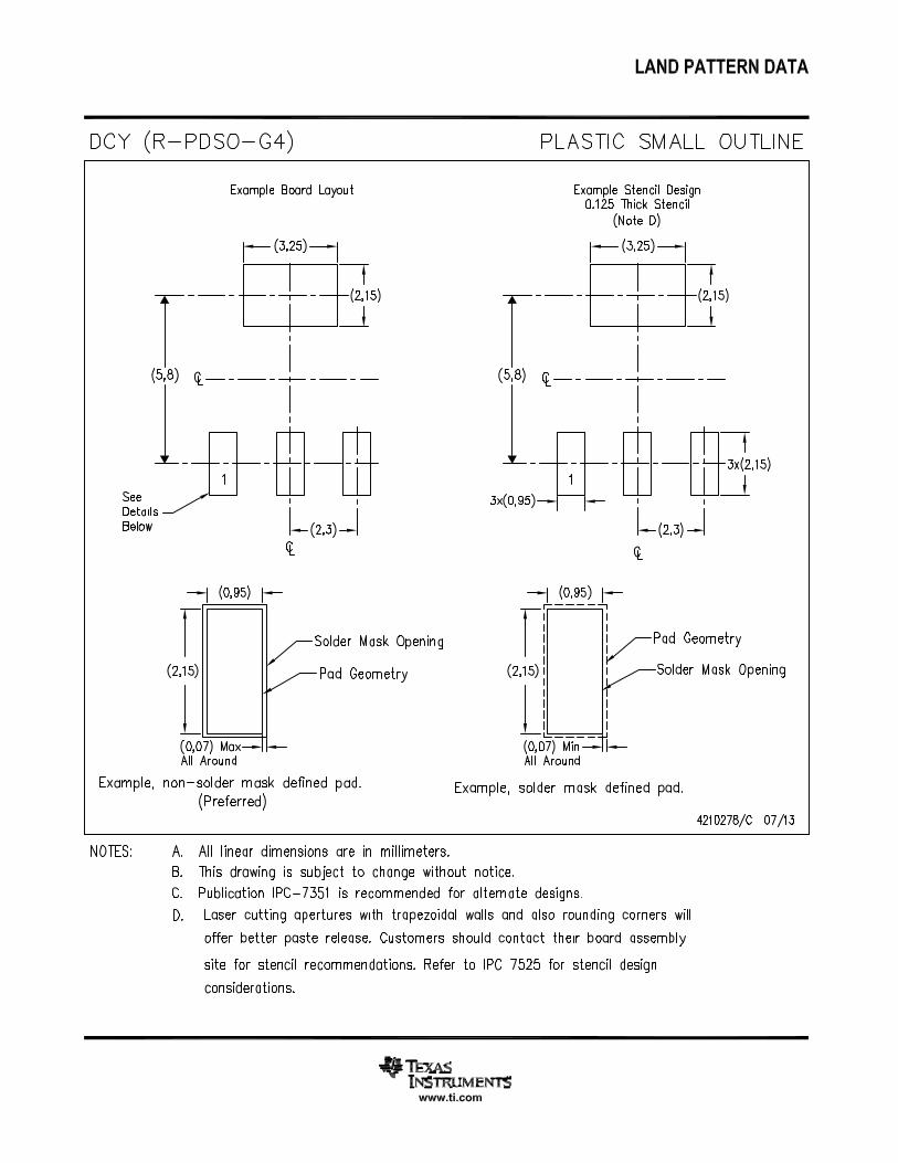
10.3 Heat Sinking DDPAK/TO-263 and SOT-223 Package PartsBoth the DDPAK/TO-263 (KTT) and SOT-223 (DCY) packages use a copper plane on the PCB and the PCBitself as a heat sink. To optimize the heat sinking ability of the plane and PCB, solder the tab of the plane.
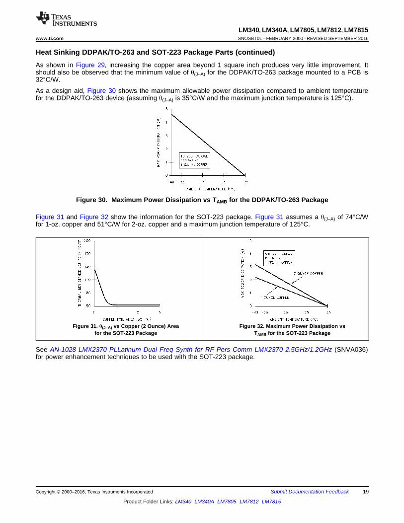
Figure 29 shows for the DDPAK/TO-263 the measured values of θ(J–A) for different copper area sizes using atypical PCB with 1-oz copper and no solder mask over the copper area used for heat sinking.
Figure 29. θ(J–A) vs Copper (1 Ounce) Area for the DDPAK/TO-263 Package
19
LM340, LM340A, LM7805, LM7812, LM7815www.ti.com SNOSBT0L –FEBRUARY 2000–REVISED SEPTEMBER 2016
Product Folder Links: LM340 LM340A LM7805 LM7812 LM7815
Submit Documentation FeedbackCopyright © 2000–2016, Texas Instruments Incorporated
Heat Sinking DDPAK/TO-263 and SOT-223 Package Parts (continued)As shown in Figure 29, increasing the copper area beyond 1 square inch produces very little improvement. Itshould also be observed that the minimum value of θ(J–A) for the DDPAK/TO-263 package mounted to a PCB is32°C/W.
As a design aid, Figure 30 shows the maximum allowable power dissipation compared to ambient temperaturefor the DDPAK/TO-263 device (assuming θ(J–A) is 35°C/W and the maximum junction temperature is 125°C).
Figure 30. Maximum Power Dissipation vs TAMB for the DDPAK/TO-263 Package
Figure 31 and Figure 32 show the information for the SOT-223 package. Figure 31 assumes a θ(J–A) of 74°C/Wfor 1-oz. copper and 51°C/W for 2-oz. copper and a maximum junction temperature of 125°C.
Figure 31. θ(J–A) vs Copper (2 Ounce) Areafor the SOT-223 Package
Figure 32. Maximum Power Dissipation vsTAMB for the SOT-223 Package
See AN-1028 LMX2370 PLLatinum Dual Freq Synth for RF Pers Comm LMX2370 2.5GHz/1.2GHz (SNVA036)for power enhancement techniques to be used with the SOT-223 package.
20
LM340, LM340A, LM7805, LM7812, LM7815SNOSBT0L –FEBRUARY 2000–REVISED SEPTEMBER 2016 www.ti.com
Product Folder Links: LM340 LM340A LM7805 LM7812 LM7815
Submit Documentation Feedback Copyright © 2000–2016, Texas Instruments Incorporated
11 Device and Documentation Support
11.1 Documentation Support
11.1.1 Related DocumentationFor related documentation, see the following:• AN-1028 LMX2370 PLLatinum Dual Freq Synth for RF Pers Comm LMX2370 2.5GHz/1.2GHz (SNVA036)• LM140K Series 3-Terminal Positive Regulators (SNVS994)
11.2 Related LinksThe table below lists quick access links. Categories include technical documents, support and communityresources, tools and software, and quick access to sample or buy.
Table 1. Related Links
PARTS PRODUCT FOLDER SAMPLE & BUY TECHNICALDOCUMENTS
TOOLS &SOFTWARE
SUPPORT &COMMUNITY
LM340 Click here Click here Click here Click here Click hereLM340A Click here Click here Click here Click here Click hereLM7805 Click here Click here Click here Click here Click hereLM7812 Click here Click here Click here Click here Click hereLM7815 Click here Click here Click here Click here Click here
11.3 Receiving Notification of Documentation UpdatesTo receive notification of documentation updates, navigate to the device product folder on ti.com. In the upperright corner, click on Alert me to register and receive a weekly digest of any product information that haschanged. For change details, review the revision history included in any revised document.
11.4 Community ResourcesThe following links connect to TI community resources. Linked contents are provided "AS IS" by the respectivecontributors. They do not constitute TI specifications and do not necessarily reflect TI's views; see TI's Terms ofUse.
TI E2E™ Online Community TI's Engineer-to-Engineer (E2E) Community. Created to foster collaborationamong engineers. At e2e.ti.com, you can ask questions, share knowledge, explore ideas and helpsolve problems with fellow engineers.
Design Support TI's Design Support Quickly find helpful E2E forums along with design support tools andcontact information for technical support.
11.5 TrademarksE2E is a trademark of Texas Instruments.All other trademarks are the property of their respective owners.
11.6 Electrostatic Discharge CautionThese devices have limited built-in ESD protection. The leads should be shorted together or the device placed in conductive foamduring storage or handling to prevent electrostatic damage to the MOS gates.
11.7 GlossarySLYZ022 — TI Glossary.
This glossary lists and explains terms, acronyms, and definitions.
21
LM340, LM340A, LM7805, LM7812, LM7815www.ti.com SNOSBT0L –FEBRUARY 2000–REVISED SEPTEMBER 2016
Product Folder Links: LM340 LM340A LM7805 LM7812 LM7815
Submit Documentation FeedbackCopyright © 2000–2016, Texas Instruments Incorporated
12 Mechanical, Packaging, and Orderable InformationThe following pages include mechanical, packaging, and orderable information. This information is the mostcurrent data available for the designated devices. This data is subject to change without notice and revision ofthis document. For browser-based versions of this data sheet, refer to the left-hand navigation.
PACKAGE OPTION ADDENDUM
www.ti.com 4-Apr-2017
Addendum-Page 1
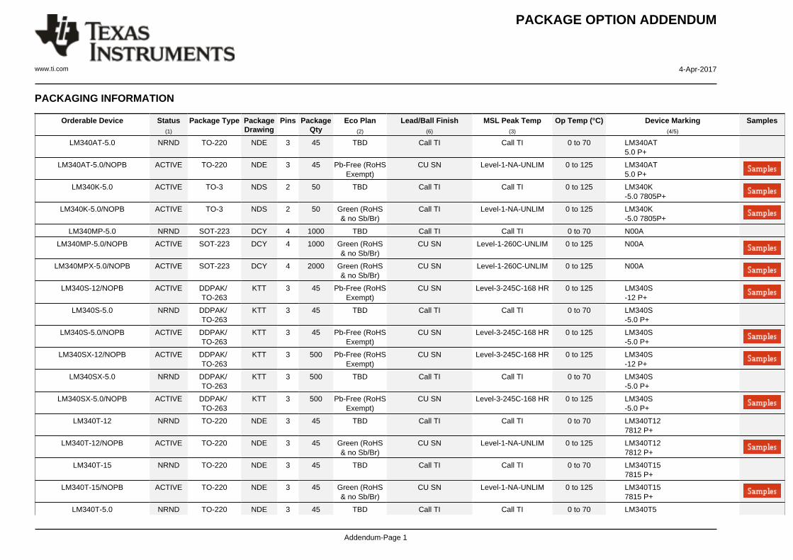
PACKAGING INFORMATION
Orderable Device Status(1)
Package Type PackageDrawing
Pins PackageQty
Eco Plan(2)
Lead/Ball Finish(6)
MSL Peak Temp(3)
Op Temp (°C) Device Marking(4/5)
Samples
LM340AT-5.0 NRND TO-220 NDE 3 45 TBD Call TI Call TI 0 to 70 LM340AT5.0 P+
LM340AT-5.0/NOPB ACTIVE TO-220 NDE 3 45 Pb-Free (RoHSExempt)
CU SN Level-1-NA-UNLIM 0 to 125 LM340AT5.0 P+
LM340K-5.0 ACTIVE TO-3 NDS 2 50 TBD Call TI Call TI 0 to 125 LM340K-5.0 7805P+
LM340K-5.0/NOPB ACTIVE TO-3 NDS 2 50 Green (RoHS& no Sb/Br)
Call TI Level-1-NA-UNLIM 0 to 125 LM340K-5.0 7805P+
LM340MP-5.0 NRND SOT-223 DCY 4 1000 TBD Call TI Call TI 0 to 70 N00A
LM340MP-5.0/NOPB ACTIVE SOT-223 DCY 4 1000 Green (RoHS& no Sb/Br)
CU SN Level-1-260C-UNLIM 0 to 125 N00A
LM340MPX-5.0/NOPB ACTIVE SOT-223 DCY 4 2000 Green (RoHS& no Sb/Br)
CU SN Level-1-260C-UNLIM 0 to 125 N00A
LM340S-12/NOPB ACTIVE DDPAK/TO-263
KTT 3 45 Pb-Free (RoHSExempt)
CU SN Level-3-245C-168 HR 0 to 125 LM340S-12 P+
LM340S-5.0 NRND DDPAK/TO-263
KTT 3 45 TBD Call TI Call TI 0 to 70 LM340S-5.0 P+
LM340S-5.0/NOPB ACTIVE DDPAK/TO-263
KTT 3 45 Pb-Free (RoHSExempt)
CU SN Level-3-245C-168 HR 0 to 125 LM340S-5.0 P+
LM340SX-12/NOPB ACTIVE DDPAK/TO-263
KTT 3 500 Pb-Free (RoHSExempt)
CU SN Level-3-245C-168 HR 0 to 125 LM340S-12 P+
LM340SX-5.0 NRND DDPAK/TO-263
KTT 3 500 TBD Call TI Call TI 0 to 70 LM340S-5.0 P+
LM340SX-5.0/NOPB ACTIVE DDPAK/TO-263
KTT 3 500 Pb-Free (RoHSExempt)
CU SN Level-3-245C-168 HR 0 to 125 LM340S-5.0 P+
LM340T-12 NRND TO-220 NDE 3 45 TBD Call TI Call TI 0 to 70 LM340T127812 P+
LM340T-12/NOPB ACTIVE TO-220 NDE 3 45 Green (RoHS& no Sb/Br)
CU SN Level-1-NA-UNLIM 0 to 125 LM340T127812 P+
LM340T-15 NRND TO-220 NDE 3 45 TBD Call TI Call TI 0 to 70 LM340T157815 P+
LM340T-15/NOPB ACTIVE TO-220 NDE 3 45 Green (RoHS& no Sb/Br)
CU SN Level-1-NA-UNLIM 0 to 125 LM340T157815 P+
LM340T-5.0 NRND TO-220 NDE 3 45 TBD Call TI Call TI 0 to 70 LM340T5
PACKAGE OPTION ADDENDUM
www.ti.com 4-Apr-2017
Addendum-Page 2
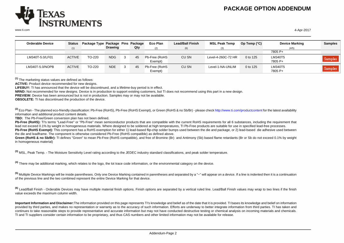
Orderable Device Status(1)
Package Type PackageDrawing
Pins PackageQty
Eco Plan(2)
Lead/Ball Finish(6)
MSL Peak Temp(3)
Op Temp (°C) Device Marking(4/5)
Samples
7805 P+
LM340T-5.0/LF01 ACTIVE TO-220 NDG 3 45 Pb-Free (RoHSExempt)
CU SN Level-4-260C-72 HR 0 to 125 LM340T57805 P+
LM340T-5.0/NOPB ACTIVE TO-220 NDE 3 45 Pb-Free (RoHSExempt)
CU SN Level-1-NA-UNLIM 0 to 125 LM340T57805 P+
(1) The marketing status values are defined as follows:ACTIVE: Product device recommended for new designs.LIFEBUY: TI has announced that the device will be discontinued, and a lifetime-buy period is in effect.NRND: Not recommended for new designs. Device is in production to support existing customers, but TI does not recommend using this part in a new design.PREVIEW: Device has been announced but is not in production. Samples may or may not be available.OBSOLETE: TI has discontinued the production of the device.
(2) Eco Plan - The planned eco-friendly classification: Pb-Free (RoHS), Pb-Free (RoHS Exempt), or Green (RoHS & no Sb/Br) - please check http://www.ti.com/productcontent for the latest availabilityinformation and additional product content details.TBD: The Pb-Free/Green conversion plan has not been defined.Pb-Free (RoHS): TI's terms "Lead-Free" or "Pb-Free" mean semiconductor products that are compatible with the current RoHS requirements for all 6 substances, including the requirement thatlead not exceed 0.1% by weight in homogeneous materials. Where designed to be soldered at high temperatures, TI Pb-Free products are suitable for use in specified lead-free processes.Pb-Free (RoHS Exempt): This component has a RoHS exemption for either 1) lead-based flip-chip solder bumps used between the die and package, or 2) lead-based die adhesive used betweenthe die and leadframe. The component is otherwise considered Pb-Free (RoHS compatible) as defined above.Green (RoHS & no Sb/Br): TI defines "Green" to mean Pb-Free (RoHS compatible), and free of Bromine (Br) and Antimony (Sb) based flame retardants (Br or Sb do not exceed 0.1% by weightin homogeneous material)
(3) MSL, Peak Temp. - The Moisture Sensitivity Level rating according to the JEDEC industry standard classifications, and peak solder temperature.
(4) There may be additional marking, which relates to the logo, the lot trace code information, or the environmental category on the device.
(5) Multiple Device Markings will be inside parentheses. Only one Device Marking contained in parentheses and separated by a "~" will appear on a device. If a line is indented then it is a continuationof the previous line and the two combined represent the entire Device Marking for that device.
(6) Lead/Ball Finish - Orderable Devices may have multiple material finish options. Finish options are separated by a vertical ruled line. Lead/Ball Finish values may wrap to two lines if the finishvalue exceeds the maximum column width.
Important Information and Disclaimer:The information provided on this page represents TI's knowledge and belief as of the date that it is provided. TI bases its knowledge and belief on informationprovided by third parties, and makes no representation or warranty as to the accuracy of such information. Efforts are underway to better integrate information from third parties. TI has taken andcontinues to take reasonable steps to provide representative and accurate information but may not have conducted destructive testing or chemical analysis on incoming materials and chemicals.TI and TI suppliers consider certain information to be proprietary, and thus CAS numbers and other limited information may not be available for release.
PACKAGE OPTION ADDENDUM
www.ti.com 4-Apr-2017
Addendum-Page 3
In no event shall TI's liability arising out of such information exceed the total purchase price of the TI part(s) at issue in this document sold by TI to Customer on an annual basis.
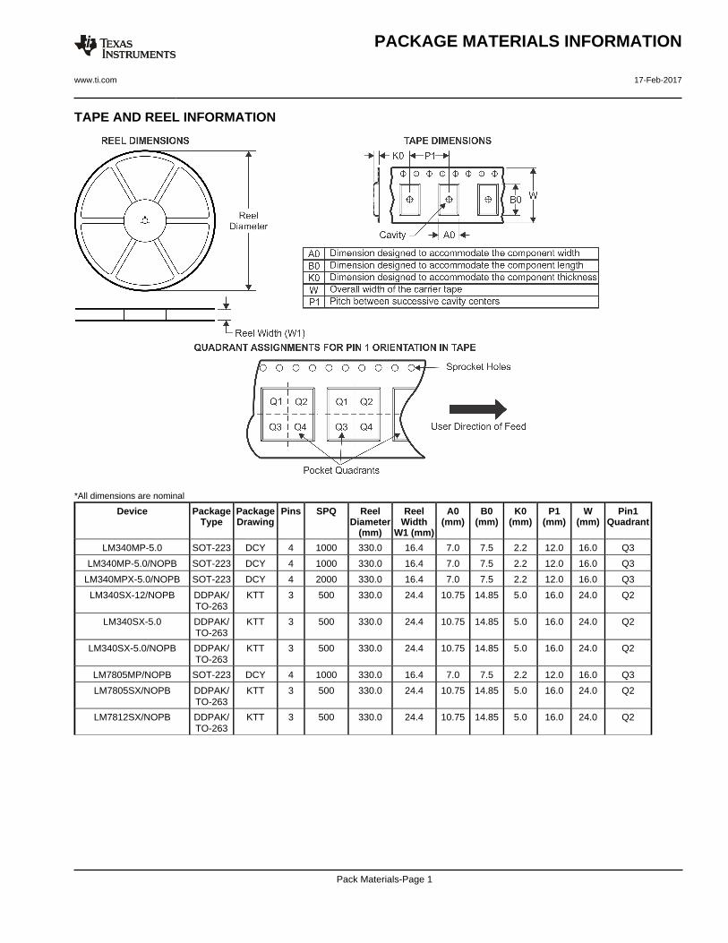
TAPE AND REEL INFORMATION
*All dimensions are nominal
Device PackageType
PackageDrawing
Pins SPQ ReelDiameter
(mm)
ReelWidth
W1 (mm)
A0(mm)
B0(mm)
K0(mm)
P1(mm)
W(mm)
Pin1Quadrant
LM340MP-5.0 SOT-223 DCY 4 1000 330.0 16.4 7.0 7.5 2.2 12.0 16.0 Q3
LM340MP-5.0/NOPB SOT-223 DCY 4 1000 330.0 16.4 7.0 7.5 2.2 12.0 16.0 Q3
LM340MPX-5.0/NOPB SOT-223 DCY 4 2000 330.0 16.4 7.0 7.5 2.2 12.0 16.0 Q3
LM340SX-12/NOPB DDPAK/TO-263
KTT 3 500 330.0 24.4 10.75 14.85 5.0 16.0 24.0 Q2
LM340SX-5.0 DDPAK/TO-263
KTT 3 500 330.0 24.4 10.75 14.85 5.0 16.0 24.0 Q2
LM340SX-5.0/NOPB DDPAK/TO-263
KTT 3 500 330.0 24.4 10.75 14.85 5.0 16.0 24.0 Q2
LM7805MP/NOPB SOT-223 DCY 4 1000 330.0 16.4 7.0 7.5 2.2 12.0 16.0 Q3
LM7805SX/NOPB DDPAK/TO-263
KTT 3 500 330.0 24.4 10.75 14.85 5.0 16.0 24.0 Q2
LM7812SX/NOPB DDPAK/TO-263
KTT 3 500 330.0 24.4 10.75 14.85 5.0 16.0 24.0 Q2
PACKAGE MATERIALS INFORMATION
www.ti.com 17-Feb-2017
Pack Materials-Page 1
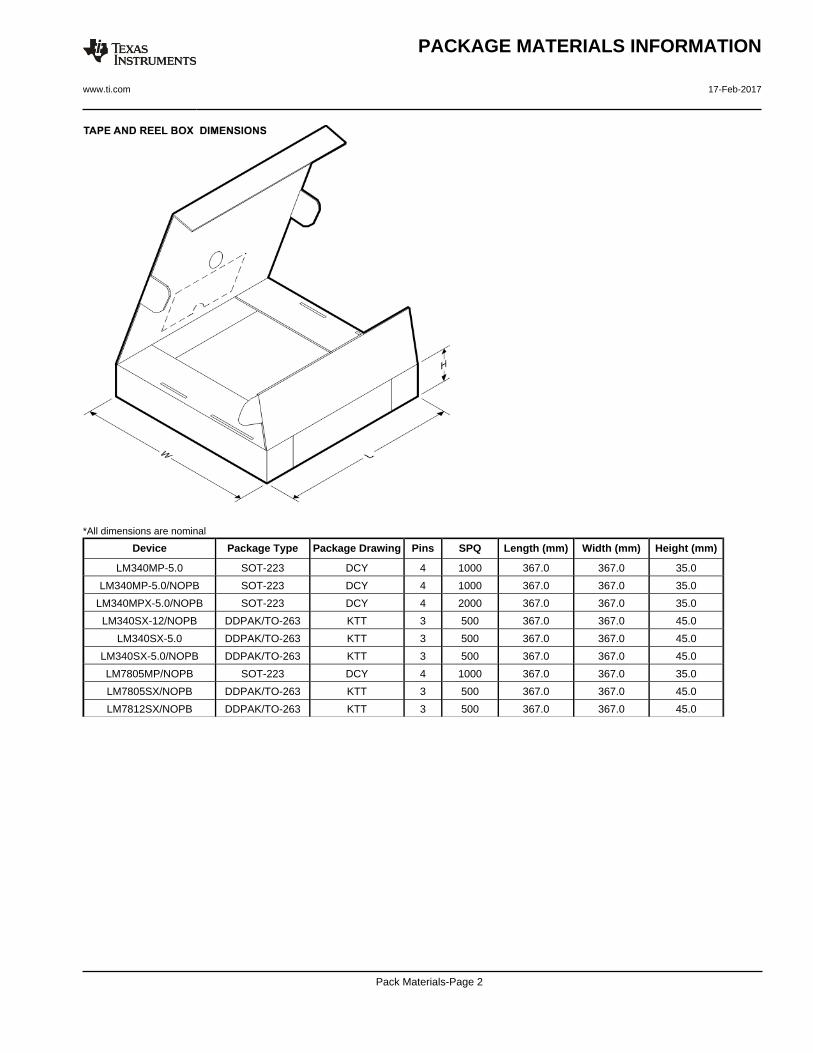
*All dimensions are nominal
Device Package Type Package Drawing Pins SPQ Length (mm) Width (mm) Height (mm)
LM340MP-5.0 SOT-223 DCY 4 1000 367.0 367.0 35.0
LM340MP-5.0/NOPB SOT-223 DCY 4 1000 367.0 367.0 35.0
LM340MPX-5.0/NOPB SOT-223 DCY 4 2000 367.0 367.0 35.0
LM340SX-12/NOPB DDPAK/TO-263 KTT 3 500 367.0 367.0 45.0
LM340SX-5.0 DDPAK/TO-263 KTT 3 500 367.0 367.0 45.0
LM340SX-5.0/NOPB DDPAK/TO-263 KTT 3 500 367.0 367.0 45.0
LM7805MP/NOPB SOT-223 DCY 4 1000 367.0 367.0 35.0
LM7805SX/NOPB DDPAK/TO-263 KTT 3 500 367.0 367.0 45.0
LM7812SX/NOPB DDPAK/TO-263 KTT 3 500 367.0 367.0 45.0
PACKAGE MATERIALS INFORMATION
www.ti.com 17-Feb-2017
Pack Materials-Page 2
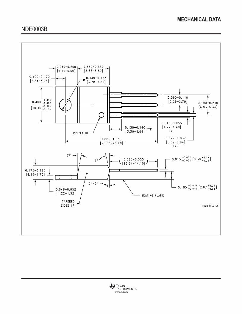
MECHANICAL DATA
NDE0003B
www.ti.com
MECHANICAL DATA
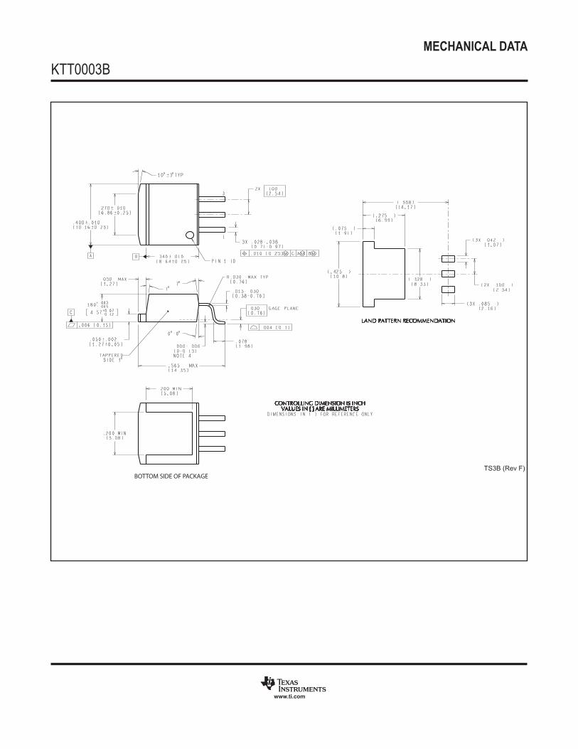
KTT0003B
www.ti.com
BOTTOM SIDE OF PACKAGETS3B (Rev F)
MECHANICAL DATA
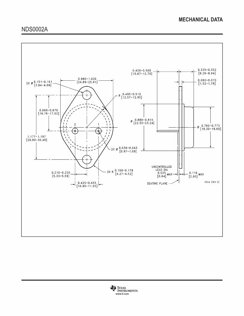
NDS0002A
www.ti.com
MECHANICAL DATA
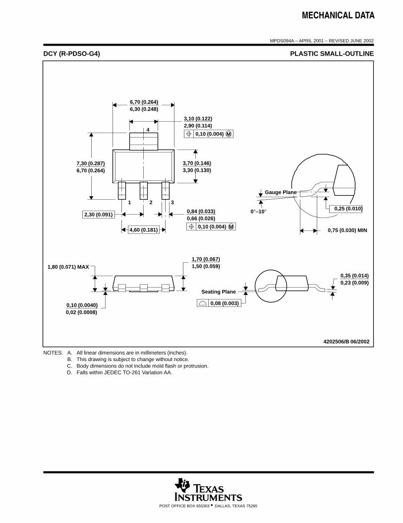
MPDS094A – APRIL 2001 – REVISED JUNE 2002
POST OFFICE BOX 655303 • DALLAS, TEXAS 75265
DCY (R-PDSO-G4) PLASTIC SMALL-OUTLINE
4202506/B 06/2002
6,30 (0.248)6,70 (0.264)
2,90 (0.114)3,10 (0.122)
6,70 (0.264)7,30 (0.287) 3,70 (0.146)
3,30 (0.130)
0,02 (0.0008)0,10 (0.0040)
1,50 (0.059)1,70 (0.067)
0,23 (0.009)0,35 (0.014)
1 2 3
4
0,66 (0.026)0,84 (0.033)
1,80 (0.071) MAX
Seating Plane
0°–10°
Gauge Plane
0,75 (0.030) MIN
0,25 (0.010)
0,08 (0.003)
0,10 (0.004) M
2,30 (0.091)
4,60 (0.181) M0,10 (0.004)
NOTES: A. All linear dimensions are in millimeters (inches).B. This drawing is subject to change without notice.C. Body dimensions do not include mold flash or protrusion.D. Falls within JEDEC TO-261 Variation AA.
MECHANICAL DATA
NDG0003F
www.ti.com
T03F (Rev B)
IMPORTANT NOTICE FOR TI DESIGN INFORMATION AND RESOURCES
Texas Instruments Incorporated (‘TI”) technical, application or other design advice, services or information, including, but not limited to,reference designs and materials relating to evaluation modules, (collectively, “TI Resources”) are intended to assist designers who aredeveloping applications that incorporate TI products; by downloading, accessing or using any particular TI Resource in any way, you(individually or, if you are acting on behalf of a company, your company) agree to use it solely for this purpose and subject to the terms ofthis Notice.TI’s provision of TI Resources does not expand or otherwise alter TI’s applicable published warranties or warranty disclaimers for TIproducts, and no additional obligations or liabilities arise from TI providing such TI Resources. TI reserves the right to make corrections,enhancements, improvements and other changes to its TI Resources.You understand and agree that you remain responsible for using your independent analysis, evaluation and judgment in designing yourapplications and that you have full and exclusive responsibility to assure the safety of your applications and compliance of your applications(and of all TI products used in or for your applications) with all applicable regulations, laws and other applicable requirements. Yourepresent that, with respect to your applications, you have all the necessary expertise to create and implement safeguards that (1)anticipate dangerous consequences of failures, (2) monitor failures and their consequences, and (3) lessen the likelihood of failures thatmight cause harm and take appropriate actions. You agree that prior to using or distributing any applications that include TI products, youwill thoroughly test such applications and the functionality of such TI products as used in such applications. TI has not conducted anytesting other than that specifically described in the published documentation for a particular TI Resource.You are authorized to use, copy and modify any individual TI Resource only in connection with the development of applications that includethe TI product(s) identified in such TI Resource. NO OTHER LICENSE, EXPRESS OR IMPLIED, BY ESTOPPEL OR OTHERWISE TOANY OTHER TI INTELLECTUAL PROPERTY RIGHT, AND NO LICENSE TO ANY TECHNOLOGY OR INTELLECTUAL PROPERTYRIGHT OF TI OR ANY THIRD PARTY IS GRANTED HEREIN, including but not limited to any patent right, copyright, mask work right, orother intellectual property right relating to any combination, machine, or process in which TI products or services are used. Informationregarding or referencing third-party products or services does not constitute a license to use such products or services, or a warranty orendorsement thereof. Use of TI Resources may require a license from a third party under the patents or other intellectual property of thethird party, or a license from TI under the patents or other intellectual property of TI.TI RESOURCES ARE PROVIDED “AS IS” AND WITH ALL FAULTS. TI DISCLAIMS ALL OTHER WARRANTIES ORREPRESENTATIONS, EXPRESS OR IMPLIED, REGARDING TI RESOURCES OR USE THEREOF, INCLUDING BUT NOT LIMITED TOACCURACY OR COMPLETENESS, TITLE, ANY EPIDEMIC FAILURE WARRANTY AND ANY IMPLIED WARRANTIES OFMERCHANTABILITY, FITNESS FOR A PARTICULAR PURPOSE, AND NON-INFRINGEMENT OF ANY THIRD PARTY INTELLECTUALPROPERTY RIGHTS.TI SHALL NOT BE LIABLE FOR AND SHALL NOT DEFEND OR INDEMNIFY YOU AGAINST ANY CLAIM, INCLUDING BUT NOTLIMITED TO ANY INFRINGEMENT CLAIM THAT RELATES TO OR IS BASED ON ANY COMBINATION OF PRODUCTS EVEN IFDESCRIBED IN TI RESOURCES OR OTHERWISE. IN NO EVENT SHALL TI BE LIABLE FOR ANY ACTUAL, DIRECT, SPECIAL,COLLATERAL, INDIRECT, PUNITIVE, INCIDENTAL, CONSEQUENTIAL OR EXEMPLARY DAMAGES IN CONNECTION WITH ORARISING OUT OF TI RESOURCES OR USE THEREOF, AND REGARDLESS OF WHETHER TI HAS BEEN ADVISED OF THEPOSSIBILITY OF SUCH DAMAGES.You agree to fully indemnify TI and its representatives against any damages, costs, losses, and/or liabilities arising out of your non-compliance with the terms and provisions of this Notice.This Notice applies to TI Resources. Additional terms apply to the use and purchase of certain types of materials, TI products and services.These include; without limitation, TI’s standard terms for semiconductor products http://www.ti.com/sc/docs/stdterms.htm), evaluationmodules, and samples (http://www.ti.com/sc/docs/sampterms.htm).
Mailing Address: Texas Instruments, Post Office Box 655303, Dallas, Texas 75265Copyright © 2017, Texas Instruments Incorporated