smt stencil design and considerations - smt & surface mount
TRANSCRIPT

STM STENCIL DESIGN AND CONSIDERATION BASE ON IPC Page 1 of 34
02/06/2007
SMT STENCIL DESIGN AND CONSIDERATIONS
Cuong Tran
Process Engineer

STM STENCIL DESIGN AND CONSIDERATION BASE ON IPC Page 2 of 34
02/06/2007
Table of Content
Subject……………………………………………………………………………………………………….Page
A Brief Discussion of PCBA Technology………………………………………………………3-5
Discussion of SMT Technology…………………………………………………………………….5-9
Role of SMT Stencil in SMT………………………………………………………………………….9-10
SMT Stencil Design……………………………………………………………………………………..10-31
SMT Printing Troubleshooting……………………………………………………………………31-33
Reference Documents………………………………………………………………………………..34

STM STENCIL DESIGN AND CONSIDERATION BASE ON IPC Page 3 of 34
02/06/2007
A BRIEF DISCUSSION OF PCBA TECHNOLOGY
Introduction:
PCBA (Printed Circuit Board Assembly) is a segment of printed circuit board technology. This
segment of printed circuit board industry is concentrated in assemble all the pieces of
electronic industry to one piece before output them to market. This segment covers:
interconnection technology, package design technology, system integration technology, board
and system test technology…etc. However, in a very brief and short description, PCBA is the
segment that concentrated in assembly all electronics and electro mechanical components on
the surface of a PCBA using metallic bonding such as: pin through-hole’s solder, surface mount
solder, or press fit interconnection.
Pin through-hole technology is the technology where components are soldered on the
board using male-female type connections. PCB (printed circuit board) bare fabrication will
provide holes that connected to all the internal circuit of the fabrication. On the other hand, the
components that will be assembled on this through-hole fabrication have male-pin type that
make by electronics packaging industry. When PCBA process applies, the components that
have male-pin will be placed in the through-hole fabrication and then solder them together by
selective wave, selective wave fixture, or dip in the liquid solder to form interconnection joins.
The picture below should illustrate the summary of this type of technology:
Similar to pin through-hole technology is press-fit components design. Press-fit
technology deviate from the idea of through hole component’s design, but not using solder to
join the component to the PCB fabrication, but have the same strength as pin through
structure. The only different between these two technologies are: 1) the male pin will be make
to fit the female hole on the PCB fabrication. 2) In order to achieve join structure, press-fit will
use pressure to put the male pin into the female hole on the fabrication in order to complete
the joining. 3) press-fit technology does not use any solder, but design in very fit and tight
dimensions between the holes of PCB fabrication and the component male pin. 4) All the
defects of this technology will come from the accuracy of the dimensions, the support tooling,

STM STENCIL DESIGN AND CONSIDERATION BASE ON IPC Page 4 of 34
02/06/2007
and the support equipment. The picture below should illustrate the summary of this type of
technology:
Last but not least, the current and widely use technology now is SMT (Surface Mount
Technology). Briefly, we can use the name of this technology to understand its use. Mounting
or solder the components on the surface of the PCB fabrication is SMT. Different between SMT
and pin through-hole technology is: while pin through-hole using liquid solder, SMT use solder
in the physical form of paste and then melt this paste in a heat oven to form the solder join.
This method of forming solder join gives SMT the advantage below: improves the time of
production, improves production capacity in term of quantity of complete product, increases
the density of components that can be mounted on the PCB fabrications, and it helps the PCBA
technology to produce products with smaller and smaller size. The picture below should
illustrate the summary of this technology:

STM STENCIL DESIGN AND CONSIDERATION BASE ON IPC Page 5 of 34
02/06/2007
This document will concentrate to discuss how to optimization and design of one of the
most important tool in SMT, SMT stencil. This tool is a printing template to deposit solder on
the surface of the SMT PCB fabrication. Although SMT stencil is just a tool that help to complete
SMT manufacture process, but it plays a very critical role in achieving high quality SMT product.
We will discuss a little more detail of SMT technology which will lead to how design a quality
stencil for SMT process.
DISCUSSION OF SMT TECHOLOGY
As we discussed in the paragraphs above, SMT technology is the technology that mount
components on the surface of PCB fabrication. This is different from pin through-hole and
press-fit technology where we mount the components through the body of PCB fabrication.
However, in reality, these technologies often use or design concurrent altogether because of
their advantages and disadvantages base of the need of applications and availabilities of
components. For understand more about SMT we need to understand the process components
of this technology. We can distinguish them by the description below: 1) SMT Printing, 2) SMT
PCB, 3) SMT Placements, and 4) SMT Reflow. However, for stencil design purpose, we will
concentrate on SMT printing and SMT PCB fabrication.
First of all, we need to understand what are differences between SMT components in
comparison with other process components? At the beginning of this document, we discussed
about pin through-hole and press-fit technology. These two technology have the similarity is
that they are both mount through the body of the PCB fabrication, but they were different
because one technology uses solder to mount, and the other technology uses pressure and
physical dimension to mount. SMT is completely different from these two types of PCBA
process because it is only mounted on the surface of the PCB fabrication. This is why it
introduced three other terms: Components termination, PCB pads, and solder paste.
Component terminations are metallic area that attaches directly on the SMT components for
the purpose is that it will be the bonding area that connected with the PCB fabrication. In
relation, PCB pads are metallic area on the PCB fabrication surface to serve the purpose of
bonding PCB interconnection to the component interconnection using SMT process. In order to
attach or bond the component’s termination and the PCB pads, solder paste or SMT epoxy are
used to help these metallic chemical bonding. The relationship between these three terms is
generally understood as the following: PCB lay-out, Component Termination design, and PCBA
bonding.
PCB fabrication is the PCBA component that lay-out all the wiring of electronic circuits. PWB
(printed wired board) and PCB are similar technologies that condense complex physical wiring

STM STENCIL DESIGN AND CONSIDERATION BASE ON IPC Page 6 of 34
02/06/2007
of circuit design into an organized manner that will give the same function as physical wiring.
The relationship of SMT component, PCB lay-out, and PCBA process are discussed in two steps
below:
1) While these wiring hide within the body of the PCB fabrication, each of the circuit
connection will represent on the surface of the PCB fabrication by PCB pads. In other
words, PCB pads are metallic surface that directly connected to the wiring within the
body of the PCB fabrication. The PCB pads are design base on the external
components pins or termination that will assemble on the PCB surface. These
components has its own function to the circuit, when they are assemble on the PCB
surface, they will connect to the internal wiring of the PCB and complete the circuit
design. Thus, if a designer use similar wiring and different component can create
different assembly and different circuit design. This is the strongest advantages of
the PCB lay-out in comparison with physical wiring. The picture below illustrated the
SMT PADs and SMT component placing on the PAD:

STM STENCIL DESIGN AND CONSIDERATION BASE ON IPC Page 7 of 34
02/06/2007
2) Between the component terminations and the PCB pad is the solder paste. After the
solder paste melted, it will form a solid solder join like the picture above, which will
connect functional components to the internal circuit wiring of PCB fabrication to
complete the circuit. the picture below should illustrate the idea:
SMT PROCESS AND BASIC EQUIPMENTS
SMT processes and basic equipments are created to achieve the manufacture capabilities of
SMT technology. In this section, we will briefly discuss some basic equipments and equipments
lay-out to perform manufacture of SMT. This discussion also refer to some basic process that
apply to SMT manufacturing.
Basic of SMT Equipments Lay-out:
Deviate from the idea of an assembly line, SMT equipments are lay-out in line. Each equipment
will provides some of the basic function and basic process requirement. First of all, let summary
SMT line lay-out. The general SMT line lay-out will have these basic equipments that follow SMT
process sequences: 1) SMT printer, 2) SMT Transport Rail Unit, 3) SMT Automated Paste
Inspection unit (Optional), 4) SMT Chip Shooter, 5) SMT Transport Rail Unit, 6) SMT IC Placer,
7) SMT Transport Rail Unit, 7) SMT Oven, 8) SMT End Transport Unit, 10) SMT Optical
Inspection: 5DX, 3DX, X-Ray, or AOI (Optional), and 11) SMT In process QA Station. We will
briefly describe in the following sections about each of equipment because they will introduce
some of the basic processes of SMT, and the picture below should illustrate the line lay-out
described above:

STM STENCIL DESIGN AND CONSIDERATION BASE ON IPC Page 8 of 34
02/06/2007
1) SMT Printer: use to print solder paste on the surface of PCB fabrication. The main tool for this
equipment is a SMT stencil with special aperture cut base on the pad lay-out of each PCB
fabrication. This meant that all will be unique for each assembly and each PCB side defend on
assembly. We will discuss more about how important is a SMT stencil and how we design them
in later discussion of this document.
2) SMT Transport Rail Unit: use to transport PCB fabrication along the line from one machine to
another. Some time, the equipment itself have build in transport rail, but additional transport
rails are used ensure smother process.
3) SMT Automated Inspection Unit (Optional): this is optional equipment because it is not required
and applied to all SMT line. Some contract manufacture use, semi automated inspection tool to
perform the quality inspection, and while the other contract manufacture might use automated
inspection. This type of SMT equipment is to help inspect quality of printing process. This type of
equipment will inspect on alignment of the printing, solder paste height, solder paste volume,
and other solder paste printing defects. This is optional equipment, but they are very important
in SMT process and SMT quality because more than 70% of solder defects begin from SMT
printing.
4) SMT Chip Shooter: some company might refer this machine as passive placement base
on their process. However, Chip Shooter is more accurate term because this machine
will place small IC such as: SOP, TSOP…etc. Most of the time, this machine will place
both small IC and passive components such as: capacitors, resistors, inductors, op-amp,
oscillators…etc. This machine will place components with really high speed, and this is
the main reason that it used to place only small IC and passive components.
5) SMT IC Placer: use to place bigger and more complicate IC such as: QFN, BGA,
LBGA…etc. This machine is armed with more optical and alignment capabilities. It can be
programmed to place IC with more termination pins and more complicated pad layout
components. It usually place part with slower speed because these part require higher
accuracy of SMT placement.
6) SMT Oven: the ideal is like a regular baking oven with extreme high temperature that
able to melt solder into liquid. After solder paste printed on the PCB fabrication, and the
placing all SMT components is done, then the assembly board will send over this oven to

STM STENCIL DESIGN AND CONSIDERATION BASE ON IPC Page 9 of 34
02/06/2007
melt the solder paste and create the solder joints between component terminations and
PCB pads.
7) Optical Inspection Units: these units are varies in capabilities and purpose because they
more concentrate on specific inspection after the solder joints came out of the oven.
They are important but optional because these equipments are purpose to enhance
quality inspection only. Many companies still use visual inspection as the main QC
methods.
8) QA and QC station: this is human operate table or station, where visual inspection
performs not by machine but human. This station also purpose to ensure defect are
recorded and fixed before moving further in PCBA processes.
The Role of SMT Stencil in Surface Mount Technology:
SMT printing begins the SMT production processes. This is the reason that it becomes the first
most important process to achieve high quality in SMT production. Although to achieve high quality in
SMT printing requires other process control such as: good condition equipment, good printing
parameter and set-up, good printing support, good print cleaning, good printing operator, and good
print tooling, but good printing stencil plays one of the most important role in the achievement of high
quality SMT PCBA process. This is why many PCBA process engineer and project engineers concentrate
to produce a good SMT stencil for printing process because it is the main tool that cannot be
maneuvered or chance unless getting a new one. At the least, if SMT production start with a good
designed SMT stencil, it will help to minimize at least 60% to 70% SMT defects besides process handling,
SMT placement, and SMT reflow. Many of PCBA engineer believe that if they can have a very good
stencil design, they can prevent 60% to 70% of SMT solder defects for the whole SMT process. This has
triggered many discussions of how to design a good SMT stencil in the PCBA industry. Each of discussion
provides different observations that help engineers to design SMT stencil. This short document will
provide an observation that will help to inform readers on how a SMT stencil design begin and
complete? What are requirements of a good SMT stencil design? What is the optimization method?
What are factors that help to produce a good SMT stencil design? And how achieve this goal with
engineering approach?
SMT STENCIL DESIGN, PREPARATION, AND CONSIDERATIONS
Many technical papers and researches introduce different approach of achieving good SMT stencil
design. In this short writing, the writer would like to introduce a systematic approach that helps
engineer or designer to review, to prevent, and to improve their stencil design. This document also
includes the discussion of how to minimize the SMT printing defects such as: over print, under print,
solder bridge…etc.

STM STENCIL DESIGN AND CONSIDERATION BASE ON IPC Page 10 of 34
02/06/2007
PREPARATION AND CONSIDERATIONS
In order to design a good SMT stencil, the writer would like to introduce a systematic approach to
achieve this goal. This system consist of four steps: CAD or GERBER review, BOM review, Standard
Suggestion Review, and PCB fabrication review. We will discuss each steps and its function:
1) CAD or GERBER Review: CAD or GERBER is always required because this information is not only
used to make stencil but for SMT placement process it is required to help SMT programming.
Usually, this information always provided.
2) BOM Review: many engineer might not think of this step as a relevant step, but it play a very
important role for stencil design process because of the information that provide in the BOM.
The information usually available provide from BOM: part packaging type, part packaging size,
and process type.
3) Standard and Suggestion Review: some of the packages have special suggestion for stencil
design from manufacture, stencil design also have certain standard design, for some companies
also available their own stencil design guideline, and at review standard will help the designer to
set his or her mind on certain type of stencil design such as NO-CLEAN or CLEAN design, LEAD or
LEAD-FREE solder printing design.
4) PCB Fabrication Review: optional but the most important step. The solder sample is not always
available to the stencil designer, but it provides many missing information that not provide in
CAD, GERBER, BOM, or Standard Guideline. The information provides by sample PCB fabrication
include: variation in dimension of PCB pad from GERBER to actually fabrication, is there any
DFM that normally not see by CAD or GERBER, and how this actual PCB fabrication impact on
the stencil design.
SMT STENCIL DESIGN
This stencil design suggestion will base on IPC-7525 Rev L that released in 2005 and IPC-7095 Rev A that
released in October 2004. The ideas and formulas mention in this document base on suggestion and
analysis of these two standards above. We will begin by looking at general guideline suggested by IPC-
7525 Rev L, and then discuss in detail with analysis of IPC-standard and then move forward to specific
application of these analysis.
IPC-7525 Rev L General Guideline and Formulas:
According to this IPC-7525L standard, two factors that help a designer to calculate and estimate the
quality of his stencil design are: Aspect Ratio and Area Ratio. However, we also introduce another factor
that not directly mention in IPC document is solder paste volume estimation.

STM STENCIL DESIGN AND CONSIDERATION BASE ON IPC Page 11 of 34
02/06/2007
1) Aspect Ratio: is the calculation of percentage that solders paste release through an aperture
onto the surface of PCB fabrication or PCB pad. This is a simplified version of area ratio. This
relationship is simply compared width of the PCB pad and thickness of stencil foil. The
standard suggests that good aspect ratio is at least greater than 1.5 or understood as 150%
solder release on the PCB pad through a aperture when the printing squeeze sweep the
solder over the aperture. This is the simplified version of area ratio when the length is much
greater than the width so the standard suggested the formula below:
𝑨𝒔𝒑𝒆𝒄𝒕 𝑹𝒂𝒕𝒊𝒐 =𝑾𝒊𝒅𝒕𝒉 𝒐𝒇 𝑨𝒑𝒆𝒓𝒕𝒖𝒓𝒆
𝑻𝒉𝒊𝒄𝒌𝒏𝒆𝒔𝒔 𝒐𝒇 𝒔𝒕𝒆𝒏𝒄𝒊𝒍 𝒇𝒐𝒊𝒍
𝑊𝑖𝑑𝑡 𝑜𝑓 𝑎𝑝𝑒𝑟𝑡𝑢𝑟𝑒 = 𝑊 𝑎𝑛𝑑 𝑇𝑖𝑐𝑘𝑛𝑒𝑠𝑠 𝑜𝑓 𝑠𝑡𝑒𝑛𝑐𝑖𝑙 𝑓𝑜𝑖𝑙 = 𝑇
𝑆𝑜𝑚𝑒𝑡𝑖𝑚𝑒 𝑊 = 𝐷 𝑖𝑛 𝑟𝑜𝑢𝑛𝑑 𝑃𝐶𝐵 𝑝𝑎𝑑,𝑤𝑒𝑟𝑒 𝑊 = 𝑊𝑖𝑑𝑡 𝑜𝑓 𝑡𝑒 𝑝𝑎𝑑,𝑎𝑛𝑑 𝐷
= 𝐷𝑖𝑎𝑚𝑒𝑡𝑒𝑟 𝑜𝑓 𝑡𝑒 𝑐𝑖𝑟𝑐𝑢𝑙𝑎𝑟 𝑝𝑎𝑑 𝑡𝑜 𝑒𝑠𝑡𝑖𝑚𝑎𝑡𝑒 𝑎𝑠𝑝𝑒𝑐𝑡 𝑟𝑎𝑡𝑖𝑜
𝑨𝒔𝒑𝒆𝒄𝒕 𝑹𝒂𝒕𝒊𝒐 =𝑾
𝑻
2) Area Ratio: is the ratio between the aperture walls and the PCB pad. This calculates the
percentage of solder release on the PCB pad with certain aperture design. The standard
suggests the good solder release is greater or at least 0.66 (66%). The description of this
calculation below:
𝐀𝐫𝐞𝐚 𝐑𝐚𝐭𝐢𝐨 =𝐀𝐫𝐞𝐚 𝐨𝐟 𝐭𝐡𝐞 𝐩𝐚𝐝
𝐀𝐫𝐞𝐚 𝐨𝐟 𝐭𝐡𝐞 𝐚𝐩𝐞𝐫𝐭𝐮𝐫𝐞 𝐰𝐚𝐥𝐥𝐬=
𝐋 ∗ 𝐖
𝟐 ∗ 𝐋+𝐖 ∗ 𝐓
𝐿 = 𝑇𝑒 𝑙𝑒𝑛𝑔𝑡 𝑜𝑓 𝑡𝑒 𝑝𝑎𝑑
𝑊 = 𝑇𝑒 𝑊𝑖𝑑𝑡 𝑜𝑓 𝑡𝑒 𝑝𝑎𝑑
𝑇 = 𝑇𝑒 𝑡𝑖𝑐𝑘𝑛𝑒𝑠𝑠 𝑜𝑓 𝑠𝑡𝑒𝑛𝑐𝑖𝑙 𝑓𝑜𝑖𝑙
3) Theoretical Solder Paste Volume: this idea was not discuss detail in IPC standard and no
special suggested formula, but it played a very important role in solder paste quality control.
Theoretical Volume is the volume of solder paste intended to deposit on the PCB pad. When
an aperture designed, there is certain amount of solder paste that intended to deposit on
the PCB pad, and this intended volume is calculated by normal volume theory. Using solder
paste volume comparison between theoretical volume and the actual volume deposited on
the PCB pad can show how accurate and how good solder release and deposit after printing
process. For example, if an aperture size 10x10 mils with a stencil thickness is 5 mils then
the theoretical volume is 500 (mils)³. For some reason, the measure volume of this aperture
is 300 (mils) ³, then it raises the question why this volume is too far different from the
intended or theory volume. The stencil designer or the engineer can go back and check if the
aperture’s cut was accurate as he designed, or was other factors that caused these two
volumes too far different from each other. Thus, understand theoretical volume can help

STM STENCIL DESIGN AND CONSIDERATION BASE ON IPC Page 12 of 34
02/06/2007
control, improve, and trouble shoot SMT printing process. The theoretical volume is thought
as the following formula:
𝐓𝐡𝐞𝐨𝐫𝐞𝐭𝐢𝐜𝐚𝐥 𝐒𝐨𝐥𝐝𝐞𝐫 𝐏𝐚𝐬𝐭𝐞 𝐕𝐨𝐥𝐮𝐦𝐞
= 𝐀𝐫𝐞𝐚 𝐨𝐟 𝐭𝐡𝐞 𝐚𝐩𝐞𝐫𝐭𝐮𝐫𝐞 ∗ 𝐓𝐡𝐢𝐜𝐤𝐧𝐞𝐬𝐬 𝐨𝐟 𝐬𝐭𝐞𝐧𝐜𝐢𝐥
Stencil Design’s Formula and Apertures:
𝑨𝒓𝒆𝒂 𝑹𝒂𝒕𝒊𝒐 =𝑨𝒓𝒆𝒂 𝒐𝒇 𝒕𝒉𝒆 𝒑𝒂𝒅
𝑨𝒓𝒆𝒂 𝒐𝒇 𝒕𝒉𝒆 𝒂𝒑𝒆𝒓𝒕𝒖𝒓𝒆 𝒘𝒂𝒍𝒍𝒔=
𝑳 ∗𝑾
𝟐 ∗ 𝑳+𝑾 ∗ 𝑻
𝐿 = 𝑇𝑒 𝑙𝑒𝑛𝑔𝑡 𝑜𝑓 𝑡𝑒 𝑝𝑎𝑑
𝑊 = 𝑇𝑒 𝑊𝑖𝑑𝑡 𝑜𝑓 𝑡𝑒 𝑝𝑎𝑑
𝑇 = 𝑇𝑒 𝑡𝑖𝑐𝑘𝑛𝑒𝑠𝑠 𝑜𝑓 𝑠𝑡𝑒𝑛𝑐𝑖𝑙 𝑓𝑜𝑖𝑙
𝑇𝑒𝑜𝑟𝑒𝑡𝑖𝑐𝑎𝑙 𝑆𝑜𝑙𝑑𝑒𝑟 𝑃𝑎𝑠𝑡𝑒 𝑉𝑜𝑙𝑢𝑚𝑒 = 𝐴𝑟𝑒𝑎 𝑜𝑓 𝑡𝑒 𝑎𝑝𝑒𝑟𝑡𝑢𝑟𝑒 ∗ 𝑇𝑖𝑐𝑘𝑛𝑒𝑠𝑠 𝑜𝑓 𝑠𝑡𝑒𝑛𝑐𝑖𝑙
Analysis of Standard Area Ratio of IPC-7525A:
When look at the suggest formula above, we see that this formula bases on rectangular
aperture because:
1) Numerator is the area of rectangle formula when L*W = Area. This suggested that this
formula bases on rectangular pad.
2) Denominator is 2*(L + W)* T or we can thought this as (T * Perimeter of rectangle).
3) If I use this analysis and look at the formula one more time, it would be like this:
𝑨𝒓𝒆𝒂 𝒓𝒂𝒕𝒊𝒐 =𝑨𝒓𝒆𝒂 𝒐𝒇 𝒓𝒆𝒄𝒕𝒂𝒏𝒈𝒖𝒍𝒂𝒓
𝑷𝒆𝒓𝒊𝒎𝒆𝒕𝒆𝒓 𝒐𝒇 𝒓𝒆𝒄𝒕𝒂𝒏𝒈𝒖𝒍𝒂𝒓 ∗ 𝑻𝒉𝒊𝒄𝒌𝒏𝒆𝒔𝒔 𝒐𝒇 𝒔𝒕𝒆𝒏𝒄𝒊𝒍=
𝑳 ∗𝑾
𝟐 ∗ 𝑳 + 𝑾 ∗ 𝑻
This wording of IPC formula does not change the formula, but give use more analysis options because in
reality, rectangular pad is not the only type of pad shape use on the PCB, and thinking this way will help
to calculate the other pad’s geometric. Before we discuss further in specific formula apply for each PCB
pad shape, we need to understand this three terms: 1) ratio 1:1, 2) extend 1:1, and 3) reduce 1:1.
1) Area ratio 1:1 means that the aperture will cut or open exact dimensions of the PCB pad.

STM STENCIL DESIGN AND CONSIDERATION BASE ON IPC Page 13 of 34
02/06/2007
2) Area Extend 1:1 means that the aperture will cut or open by extend each dimension of the
PCB pad one. The picture below should illustrate the idea:
𝐿 𝑎 𝑤𝑖𝑑𝑡 𝑜𝑓 𝑎𝑝𝑒𝑟𝑡𝑢𝑟𝑒 = 𝐿 𝑝 𝑙𝑒𝑛𝑔𝑡 𝑜𝑓 𝑃𝐶𝐵 𝑝𝑎𝑑 + 1
𝑊 𝑎 𝑤𝑖𝑑𝑡 𝑜𝑓 𝑎𝑝𝑒𝑟𝑡𝑢𝑟𝑒 = 𝑊 𝑝 𝑊𝑖𝑑𝑡 𝑜𝑓 𝑡𝑒 𝑃𝐶𝐵 𝑝𝑎𝑑 + 1
3) Area reduce 1:1 means that the aperture will cut or open after reduce all dimensions of PCB
pad to 1 unit. The idea should illustrate in the picture below:
𝐿 𝑎 𝑤𝑖𝑑𝑡 𝑜𝑓 𝑎𝑝𝑒𝑟𝑡𝑢𝑟𝑒 = 𝐿 𝑝 𝑙𝑒𝑛𝑔𝑡 𝑜𝑓 𝑃𝐶𝐵 𝑝𝑎𝑑 − 1
𝑊 𝑎 𝑤𝑖𝑑𝑡 𝑜𝑓 𝑎𝑝𝑒𝑟𝑡𝑢𝑟𝑒 = 𝑊 𝑝 𝑊𝑖𝑑𝑡 𝑜𝑓 𝑡𝑒 𝑃𝐶𝐵 𝑝𝑎𝑑 − 1
Formulas for Popular Aperture:
In this following section, we will discuss in detail of some popular aperture use in the industry. We will
assume that these formulas will not apply for not 1:1 design.
1) Rectangular Pad with Rectangular Aperture:

STM STENCIL DESIGN AND CONSIDERATION BASE ON IPC Page 14 of 34
02/06/2007
This formula applies for rectangular pad with the design of rectangular aperture:
=𝑨𝒓𝒆𝒂 𝒐𝒇 𝒕𝒉𝒆 𝒓𝒆𝒄𝒕𝒂𝒏𝒈𝒖𝒍𝒂𝒓 𝑷𝒂𝒅
(𝑷𝒆𝒓𝒊𝒎𝒆𝒕𝒆𝒓 𝒐𝒇 𝒓𝒆𝒄𝒕𝒂𝒏𝒈𝒖𝒍𝒂𝒓 𝒂𝒑𝒆𝒓𝒕𝒖𝒓𝒆∗ 𝑻𝒉𝒊𝒄𝒌𝒏𝒆𝒔𝒔 𝒐𝒇 𝒔𝒕𝒆𝒏𝒄𝒊𝒍 𝒇𝒐𝒊𝒍)
𝑨𝒓𝒆𝒂 𝒓𝒂𝒕𝒊𝒐 𝒂𝒄𝒄𝒐𝒓𝒅𝒊𝒏𝒈 𝒕𝒐 𝑰𝑷𝑪 =𝑳 ∗𝑾
𝟐 ∗ 𝑳𝒎 +𝑾𝒎 ∗ 𝑻
𝐿𝑚 = 𝐿 𝑖𝑛 1: 1 𝑟𝑎𝑡𝑖𝑜, 𝑜𝑡𝑒𝑟 𝑐𝑎𝑠𝑒 𝐿𝑚 ≠ 𝐿
𝑇𝑒𝑜𝑟𝑒𝑡𝑖𝑐𝑎𝑙 𝑣𝑜𝑙𝑢𝑚𝑒 𝑓𝑜𝑟 𝑟𝑒𝑐𝑡𝑎𝑛𝑔𝑢𝑙𝑎𝑟 𝑎𝑝𝑒𝑟𝑡𝑢𝑟𝑒 = 𝐿𝑚 ∗𝑊𝑚 ∗ 𝑇 = 𝑡𝑖𝑐𝑘𝑛𝑒𝑠𝑠 𝑜𝑓 𝑠𝑡𝑒𝑛𝑐𝑖𝑙 𝑓𝑜𝑖𝑙
2) Square Pad with Square Aperture:
This formula applies for square PCB pad with square aperture design:
𝐴𝑟𝑒𝑎 𝑟𝑎𝑡𝑖𝑜 𝑜𝑓 𝑠𝑞𝑢𝑎𝑟𝑒 𝑎𝑝𝑒𝑟𝑡𝑢𝑟𝑒
=𝐴𝑟𝑒𝑎 𝑜𝑓 𝑠𝑞𝑢𝑎𝑟𝑒 𝑝𝑎𝑑
𝑃𝑒𝑟𝑖𝑚𝑒𝑡𝑒𝑟 𝑜𝑓 𝑠𝑝𝑢𝑎𝑟𝑒 𝑎𝑝𝑒𝑟𝑡𝑢𝑟𝑒 ∗ 𝑇𝑖𝑐𝑘𝑛𝑒𝑠𝑠 𝑜𝑓 𝑠𝑡𝑒𝑛𝑐𝑖𝑙 𝑓𝑜𝑖𝑙
𝐴𝑟𝑒𝑎 𝑟𝑎𝑡𝑖𝑜 𝑓𝑜𝑟 𝑠𝑞𝑢𝑎𝑟𝑒 𝑎𝑝𝑒𝑟𝑡𝑢𝑟𝑒 =𝐿2
4𝐿𝑚 ∗ 𝑇
𝐿 = 𝐿𝑒𝑛𝑔𝑡 𝑜𝑓 𝑡𝑒 𝑃𝐶𝐵 𝑠𝑞𝑢𝑎𝑟𝑒 𝑝𝑎𝑑
𝑇 = 𝑇𝑖𝑐𝑘𝑛𝑒𝑠𝑠 𝑜𝑓 𝑠𝑡𝑒𝑛𝑐𝑖𝑙 𝑓𝑜𝑖𝑙
𝐿𝑚 = 𝐿 𝑖𝑛 1: 1 𝑟𝑎𝑡𝑖𝑜𝑛, 𝑏𝑢𝑡 𝑓𝑜𝑟 𝑜𝑡𝑒𝑟 𝑐𝑎𝑠𝑒 𝐿𝑚 ≠ 𝐿
3) Circular Pad with Circular Aperture:
This formula applies for circular PCB pad with circular aperture design:
𝐴𝑟𝑒𝑎 𝑟𝑎𝑡𝑖𝑜 𝑜𝑓 𝑐𝑖𝑟𝑐𝑢𝑙𝑎𝑟 𝑎𝑝𝑒𝑟𝑡𝑢𝑟𝑒 =𝐴𝑟𝑒𝑎 𝑜𝑓 𝑡𝑒 𝑐𝑖𝑟𝑐𝑢𝑙𝑎𝑟 𝑝𝑎𝑑
(𝐶𝑖𝑟𝑐𝑢𝑚𝑓𝑒𝑟𝑒𝑛𝑐𝑒 𝑜𝑓 𝑡𝑒 𝑐𝑖𝑟𝑐𝑢𝑙𝑎𝑟 𝑎𝑝𝑒𝑟𝑡𝑢𝑟𝑒∗ 𝑇𝑖𝑐𝑘𝑛𝑒𝑠𝑠 𝑜𝑓 𝑠𝑡𝑒𝑛𝑐𝑖𝑙 𝑓𝑜𝑖𝑙)

STM STENCIL DESIGN AND CONSIDERATION BASE ON IPC Page 15 of 34
02/06/2007
𝑨𝒓𝒆𝒂 𝒓𝒂𝒕𝒊𝒐 𝒐𝒇 𝒄𝒊𝒓𝒄𝒖𝒍𝒂𝒓 𝒂𝒑𝒆𝒓𝒕𝒖𝒓𝒆 =𝝅 ∗ (
𝑫𝟐)𝟐
𝛑 ∗ 𝐃𝐦 ∗ 𝐓
𝐷 = 𝐷𝑖𝑎𝑚𝑒𝑡𝑒𝑟 𝑜𝑓 𝑡𝑒 𝑃𝐶𝐵 𝑝𝑎𝑑
𝐷𝑚 = 𝐷 𝑖𝑛 1: 1 𝑟𝑎𝑡𝑖𝑜, 𝑜𝑡𝑒𝑟 𝑐𝑎𝑠𝑒 𝐷𝑚 ≠ 𝐷
𝑻𝒉𝒆𝒐𝒓𝒆𝒕𝒊𝒄𝒂𝒍 𝒗𝒐𝒍𝒖𝒎𝒆 𝒐𝒇 𝒄𝒊𝒓𝒄𝒖𝒍𝒂𝒓 𝒂𝒑𝒆𝒓𝒕𝒖𝒓𝒆 = 𝝅 ∗ 𝑫𝒎
𝟐 𝟐
∗ 𝑻 = 𝑻𝒉𝒊𝒄𝒌𝒏𝒆𝒔𝒔 𝒐𝒇 𝒔𝒕𝒆𝒏𝒄𝒊𝒍 𝒇𝒐𝒊𝒍
4) Circular Pad with Square Aperture with round corner trim:
Generally, we can use the formula below to estimate area ratio:
𝑨𝒓𝒆𝒂 𝒓𝒂𝒕𝒊𝒐 𝒇𝒐𝒓 𝒔𝒒𝒖𝒂𝒓𝒆 𝒂𝒑𝒆𝒓𝒕𝒖𝒓𝒆 𝒐𝒗𝒆𝒓 𝒓𝒐𝒖𝒏𝒅 𝒑𝒂𝒅 =𝝅 ∗
𝑫𝟐
𝟐
𝑳𝒎 𝟐 ∗ 𝑻
𝐷 = 𝑑𝑖𝑎𝑚𝑒𝑡𝑒𝑟 𝑜𝑓 𝑡𝑒 𝑟𝑜𝑢𝑛𝑑 𝑝𝑎𝑑
𝐿𝑚 = 𝐷 − 𝑠𝑜𝑚𝑒 𝑢𝑛𝑖𝑡𝑠 𝑐𝑜𝑠𝑒 𝑏𝑦 𝑡𝑒 𝑠𝑡𝑒𝑛𝑐𝑖𝑙 𝑑𝑒𝑠𝑖𝑔𝑛𝑒𝑟
In some most of the case, the four corners of the square will be trim off to prevent excess
printing solder that might create solder balls. We will discuss in detail for this aperture
design.
Explanation of this formula:

STM STENCIL DESIGN AND CONSIDERATION BASE ON IPC Page 16 of 34
02/06/2007
These two diagrams help to explain the estimation of round corner square aperture over the circular
PCB pad. First let analyze the diagrams, the length of square equal to the diameter of the circle or this
length can be any number that the designer choose. For this analysis, we will use the length of square
equal the diameter.
A) Analysis of above diagrams and theoretical volume:
𝐿𝑠 = 𝐷,𝑤𝑒𝑟𝑒 𝐿𝑠 = 𝑙𝑒𝑛𝑔𝑡 𝑜𝑓 𝑠𝑞𝑢𝑎𝑟𝑒 𝑎𝑛𝑑 𝐷 = 𝐷𝑖𝑎𝑚𝑒𝑡𝑒𝑟 𝑜𝑓 𝑡𝑒 𝑐𝑖𝑟𝑐𝑢𝑙𝑎𝑟 𝑝𝑎𝑑.
𝑨𝒕 =𝑳𝒔𝟐
𝟐,𝑤𝑒𝑟𝑒 𝐴𝑡 = 𝐴𝑟𝑒𝑎 𝑜𝑓 𝑡𝑟𝑖𝑎𝑛𝑔𝑙𝑒 𝑏𝑒𝑓𝑜𝑟𝑒 𝑟𝑜𝑢𝑛𝑑 𝑐𝑜𝑟𝑛𝑒𝑟 𝑡𝑟𝑖𝑚𝑚𝑒𝑑 𝑎𝑛𝑑 𝐿𝑠2
= 𝐴𝑟𝑒𝑎 𝑜𝑓 𝑡𝑒 𝑠𝑞𝑢𝑎𝑟𝑒 𝑎𝑝𝑒𝑟𝑡𝑢𝑟𝑒 𝑏𝑒𝑓𝑜𝑟𝑒 𝑡𝑟𝑖𝑚𝑏𝑙𝑒.
𝐴𝑥 = 𝜃
360 ∗ 𝜋 ∗
𝐿𝑠
2
2
𝐴𝑥 = 𝑎𝑟𝑒𝑎 𝑜𝑓 𝑡𝑒 𝑟𝑜𝑢𝑛𝑑 𝑐𝑜𝑟𝑛𝑒𝑟 𝑤𝑖𝑡 𝑡𝑒 𝑎𝑛𝑔𝑙𝑒 𝜃
= 60°𝑜𝑟 30° 𝑑𝑒𝑝𝑒𝑛𝑑 𝑜𝑛 𝑡𝑒 𝑐𝑜𝑖𝑐𝑒 𝑜𝑓 𝑑𝑒𝑠𝑖𝑔𝑛𝑒𝑟.
For example: If a designer want the square aperture with round corner over a circular PCB pad
with the diameter = 10 mils. He or she can give the instruction below:
Open Square aperture with the length of 10x10 and round corner 3 or 6. The “3 or 6” means
30 degree or 60 degree for the central angle of round corner section.
Thus, the area of the trimmed corner for the triangle in the above picture is:
𝐴𝑟𝑒𝑎 𝑜𝑓 𝑡𝑟𝑖𝑚𝑚𝑒𝑑 𝑐𝑜𝑟𝑛𝑒𝑟1
2𝐴𝑦 = 𝐴𝑡 − 2𝐴𝑥
The total round corner areas were trimmed:
𝑇𝑜𝑡𝑎𝑙 𝑎𝑟𝑒𝑎 𝑤𝑒𝑟𝑒 𝑡𝑟𝑖𝑚𝑚𝑒𝑑 𝑜𝑓𝑓 𝑓𝑟𝑜𝑚 𝑠𝑞𝑢𝑎𝑟𝑒 𝑎𝑝𝑒𝑟𝑡𝑢𝑟𝑒 = 𝐿𝑠2 − 4𝐴𝑦

STM STENCIL DESIGN AND CONSIDERATION BASE ON IPC Page 17 of 34
02/06/2007
𝑻𝒉𝒆𝒐𝒓𝒆𝒕𝒊𝒄𝒂𝒍 𝑽𝒐𝒍𝒖𝒎𝒆 𝒇𝒐𝒓 𝒓𝒐𝒖𝒏𝒅 𝒄𝒐𝒓𝒏𝒆𝒓 𝒔𝒒𝒖𝒂𝒓𝒆 𝒂𝒑𝒆𝒓𝒕𝒖𝒓𝒆 = (𝑳𝒔𝟐 − 𝟒𝑨𝒚)*T
𝑇 = 𝑡𝑖𝑐𝑘𝑛𝑒𝑠𝑠 𝑜𝑓 𝑠𝑡𝑒𝑛𝑐𝑖𝑙 𝑓𝑜𝑖𝑙
Please look at the analysis picture below:
These are calculations for each factor in the perimeter formula:
𝐴𝑟𝑐 𝐿𝑒𝑛𝑔𝑡 𝑡𝑎𝑡 𝑏𝑒𝑐𝑜𝑚𝑒 𝑟𝑜𝑢𝑛𝑑 𝑐𝑜𝑟𝑛𝑒𝑟 = 𝐿𝑎 = 𝐿𝑠
2 ∗ 𝜃
Thus, the perimeter:
𝑃𝑒𝑟𝑖𝑚𝑒𝑡𝑒𝑟 𝑜𝑓 𝑡𝑒 𝑠𝑞𝑢𝑎𝑟𝑒 𝑟𝑜𝑢𝑛𝑑 𝑐𝑜𝑟𝑛𝑒𝑟𝑠 = 𝑃𝑠 = 4𝐿𝑠 − 4𝐿𝑎
B) Area Ratio for Round Corner Square Aperture over circular PCB pad:
𝑨𝒓𝒆𝒂 𝒓𝒂𝒕𝒊𝒐 𝒇𝒐𝒓 𝒓𝒐𝒖𝒏𝒅 𝒄𝒐𝒓𝒏𝒆𝒓 𝒔𝒒𝒖𝒂𝒓𝒆 𝒂𝒑𝒆𝒓𝒕𝒖𝒓𝒆 =𝝅 ∗
𝑫𝟐
𝟐
𝑷𝒔 ∗ 𝑻
𝐷 = 𝐷𝑖𝑎𝑚𝑒𝑡𝑒𝑟 𝑜𝑓 𝑡𝑒 𝑐𝑖𝑟𝑐𝑢𝑙𝑎𝑟 𝑃𝐶𝐵 𝑝𝑎𝑑
𝑃𝑠 = 𝑃𝑒𝑟𝑖𝑚𝑒𝑡𝑒𝑟 𝑜𝑓 𝑡𝑒 𝑆𝑞𝑢𝑎𝑟𝑒 𝑎𝑛𝑑 𝑅𝑜𝑢𝑛𝑑 𝑐𝑜𝑟𝑛𝑒𝑟𝑠
𝑇 = 𝑇𝑖𝑐𝑘𝑛𝑒𝑠𝑠 𝑜𝑓 𝑡𝑒 𝑠𝑡𝑒𝑛𝑐𝑖𝑙 𝑓𝑜𝑖𝑙
5) Rectangular Pad with Home-base Aperture

STM STENCIL DESIGN AND CONSIDERATION BASE ON IPC Page 18 of 34
02/06/2007
Home-base aperture is suggested on the right picture by IPC standard. On the left, is
the analysis picture base of this suggestion because it is critical to our discussion of
home-base aperture’s shape?
𝑃𝑒𝑟𝑖𝑚𝑒𝑡𝑒𝑟 𝑜𝑓 𝑡𝑟𝑖𝑎𝑔𝑙𝑒 = 𝐿𝑎 + 𝐿𝑏 + 𝐿𝑐
𝑃𝑒𝑟𝑖𝑚𝑒𝑡𝑒𝑟 𝑜𝑓 𝑟𝑒𝑐𝑡𝑎𝑛𝑔𝑙𝑒 = 𝑊𝑖𝑑𝑡 𝑜𝑓 𝑝𝑎𝑑 + 𝐿𝑓 ∗ 2
If I use the left picture to calculate, my relative length La, Lb, Lc lengths are
understand as follow:
√𝐿𝑎² = (1
3𝐿)2 + (
1
2𝐿𝑐)2
𝐿𝑏2 = (1
3𝐿)2 + (
1
2𝐿𝑐)²
𝐿𝑐 = 𝑤𝑖𝑑𝑡 𝑜𝑓 𝑡𝑒 𝑝𝑎𝑑
𝐿𝑓 =2
3𝑙𝑒𝑛𝑔𝑡 𝑜𝑓 𝑡𝑒 𝑝𝑎𝑑
𝐿𝑒 =1
3𝑜𝑓 𝑙𝑒𝑛𝑔𝑡 𝑜𝑓 𝑡𝑒 𝑝𝑎𝑑
Perimeter of the home-base aperture is:
𝑃𝑒𝑟𝑖𝑚𝑒𝑡𝑒𝑟 𝑜𝑓 𝑜𝑚𝑒𝑏𝑎𝑠𝑒 𝑎𝑝𝑒𝑟𝑡𝑢𝑟𝑒 = √𝐿𝑎 + √𝐿𝑏 + 𝐿𝑐 + 𝐿𝑓
Area ratio of the home-base:
𝐴𝑟𝑒𝑎 𝑟𝑎𝑡𝑖𝑜 𝑜𝑓 𝑜𝑚𝑒𝑏𝑎𝑠𝑒 𝑎𝑝𝑒𝑟𝑡𝑢𝑟𝑒
=𝐴𝑟𝑒𝑎 𝑜𝑓 𝑟𝑒𝑐𝑡𝑎𝑛𝑔𝑢𝑙𝑎𝑟 𝑝𝑎𝑑
𝑃𝑒𝑟𝑖𝑚𝑒𝑡𝑒𝑟 𝑜𝑓 𝑜𝑚𝑒𝑏𝑎𝑠𝑒 ∗ 𝑇𝑖𝑐𝑘𝑛𝑒𝑠𝑠 𝑜𝑓 𝑠𝑡𝑒𝑛𝑐𝑖𝑙 𝑓𝑜𝑖𝑙

STM STENCIL DESIGN AND CONSIDERATION BASE ON IPC Page 19 of 34
02/06/2007
𝑨𝒓𝒆𝒂 𝒓𝒂𝒕𝒊𝒐 𝒐𝒇 𝒉𝒐𝒎𝒆𝒃𝒂𝒔𝒆 =𝑳 ∗ 𝑳𝒄
√𝑳𝒂+ √𝑳𝒃+ (𝟐 ∗ 𝒍𝒇) + 𝑳𝒄 ∗ 𝑻
Theoretical volume for home-base aperture:
𝑇𝑒𝑜𝑟𝑦 𝑣𝑜𝑙𝑢𝑚𝑒 𝑓𝑜𝑟 𝑜𝑚𝑒𝑏𝑎𝑠𝑒 𝑎𝑝𝑒𝑟𝑡𝑢𝑟𝑒
= 𝐴𝑟𝑒𝑎 𝑜𝑓 𝑡𝑟𝑖𝑎𝑛𝑔𝑙𝑒 + 𝐴𝑟𝑒𝑎 𝑜𝑓 𝑟𝑒𝑐𝑡𝑎𝑛𝑔𝑙𝑒
∗ 𝑇𝑖𝑐𝑘𝑛𝑒𝑠𝑠 𝑜𝑓 𝑠𝑡𝑒𝑛𝑐𝑖𝑙 𝑓𝑜𝑖𝑙
𝑻𝒉𝒆𝒐𝒓𝒆𝒕𝒊𝒄𝒂𝒍 𝒗𝒐𝒍𝒖𝒎𝒆 𝒇𝒐𝒓 𝒉𝒐𝒎𝒆𝒃𝒂𝒔𝒆 𝒂𝒑𝒆𝒓𝒕𝒖𝒓𝒆 = 𝟏
𝟐𝒍𝒆 ∗ 𝑳𝒄 ∗ 𝑻
6) Rectangular Pad with Bow Tie Aperture
The picture on the right is the suggestion by IPC, and the picture on the left is the
analysis base on this suggestion. Thus, the relative calculations are:
𝐿𝑎2 = (0.1 𝐿𝑒𝑛𝑔𝑡 𝑜𝑓 𝑝𝑎𝑑 𝑜𝑟 0.2 𝑙𝑒𝑛𝑔𝑡 𝑜𝑓 𝑝𝑎𝑑)2 + (1
2𝑤𝑖𝑑𝑡 𝑜𝑓 𝑝𝑎𝑑)2
√𝐿𝑏² = 0.1 𝑙𝑒𝑛𝑔𝑡 𝑜𝑓 𝑝𝑎𝑑 𝑜𝑟 0.2 𝑙𝑒𝑛𝑔𝑡 𝑜𝑓 𝑝𝑎𝑑 2 + (1
2𝑤𝑖𝑑𝑡 𝑜𝑓 𝑝𝑎𝑑)
Thus, perimeter of bow tie or inverted home base aperture:
𝑃𝑒𝑟𝑖𝑚𝑒𝑡𝑒𝑟 𝑜𝑓 𝑏𝑜𝑤 𝑡𝑖𝑒 = 𝐿𝑎2 + 𝐿𝑏2 +𝑊 + 2𝐿
Area ratio calculation as follow:
𝐴𝑟𝑒𝑎 𝑟𝑎𝑡𝑖𝑜 𝑓𝑜𝑟 𝑏𝑜𝑤 𝑡𝑖𝑒 =𝑎𝑟𝑒𝑎 𝑜𝑓 𝑟𝑒𝑐𝑡𝑎𝑛𝑔𝑢𝑙𝑎𝑟 𝑝𝑎𝑑
𝑝𝑒𝑟𝑖𝑚𝑒𝑡𝑒𝑟 𝑜𝑓 𝑏𝑜𝑤 𝑡𝑖𝑒
𝑨𝒓𝒆𝒂 𝒓𝒂𝒕𝒊𝒐 𝒇𝒐𝒓 𝒃𝒐𝒘 𝒕𝒊𝒆 =𝑳 ∗ 𝑾
√𝑳𝒂𝟐 + √𝑳𝒃𝟐 +𝑾+ 𝟐𝑳
Theory Volume for bow tie:
𝑇𝑒𝑜𝑟𝑦 𝑣𝑜𝑙𝑢𝑚𝑒 𝑓𝑜𝑟 𝑏𝑜𝑤 𝑡𝑖𝑒 𝑎𝑝𝑒𝑟𝑡𝑢𝑟𝑒
= 𝐴𝑟𝑒𝑎 𝑜𝑓 𝑟𝑒𝑐𝑡𝑎𝑛𝑔𝑢𝑙𝑎𝑟 𝑝𝑎𝑑 − 𝑏𝑜𝑤 𝑡𝑖𝑒 𝑎𝑟𝑒𝑎 𝑜𝑟 𝑡𝑟𝑖𝑎𝑛𝑔𝑙𝑒 𝑎𝑟𝑒𝑎
∗ 𝑇𝑖𝑐𝑘𝑛𝑒𝑠𝑠 𝑜𝑓 𝑠𝑡𝑒𝑛𝑐𝑖𝑙 𝑓𝑜𝑖𝑙

STM STENCIL DESIGN AND CONSIDERATION BASE ON IPC Page 20 of 34
02/06/2007
𝑻𝒉𝒆𝒐𝒓𝒆𝒕𝒊𝒄𝒂𝒍 𝒗𝒐𝒍𝒖𝒎𝒆 𝒇𝒐𝒓 𝒃𝒐𝒘 𝒕𝒊𝒆 = 𝑳 ∗𝑾 − 𝟏
𝟐 𝟎.𝟏𝑳 𝒐𝒓 𝟎.𝟐𝑳 ∗𝑾 ∗ 𝑻
7) Rectangular PCB Pad with Single Side Oblong Aperture:
The picture on the right is oblong design suggested by IPC, and on the right is the analysis
diagram of this suggestion. Thus, base on this analysis, oblong design calculations as follow:
Factors:
Dm = Diameter of imagination Dm = Width of the Pad = W
One side oblong is haft of the circle added on one side of the pad as aperture shape. Thus,
relative length calculation as follow:
𝐷𝑚 = 𝑊
𝐿𝑎 = 𝐿 − 𝐷𝑚 𝑜𝑟 𝐿 −𝑊
Perimeter of the oblong:
STM STENCIL DESIGN AND CONSIDERATION BASE ON IPC Page 21 of 34
02/06/2007
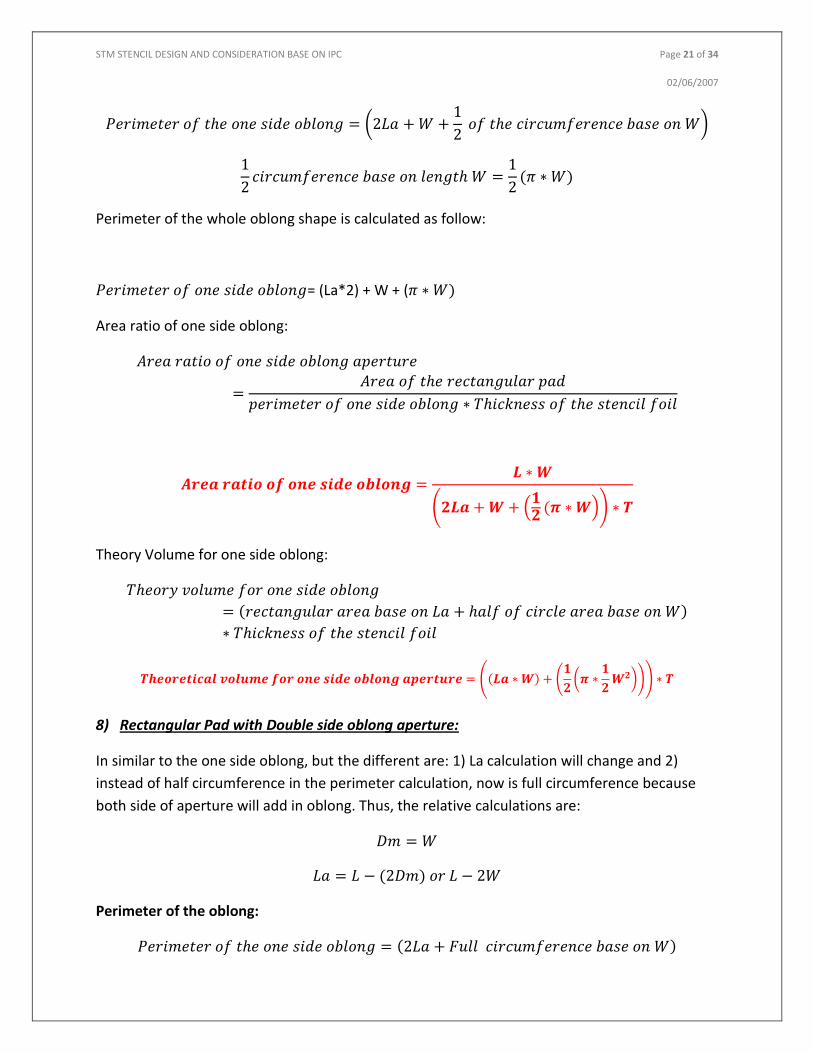
𝑃𝑒𝑟𝑖𝑚𝑒𝑡𝑒𝑟 𝑜𝑓 𝑡𝑒 𝑜𝑛𝑒 𝑠𝑖𝑑𝑒 𝑜𝑏𝑙𝑜𝑛𝑔 = 2𝐿𝑎 +𝑊 +1
2 𝑜𝑓 𝑡𝑒 𝑐𝑖𝑟𝑐𝑢𝑚𝑓𝑒𝑟𝑒𝑛𝑐𝑒 𝑏𝑎𝑠𝑒 𝑜𝑛 𝑊
1
2𝑐𝑖𝑟𝑐𝑢𝑚𝑓𝑒𝑟𝑒𝑛𝑐𝑒 𝑏𝑎𝑠𝑒 𝑜𝑛 𝑙𝑒𝑛𝑔𝑡 𝑊 =
1
2(𝜋 ∗𝑊)
Perimeter of the whole oblong shape is calculated as follow:
𝑃𝑒𝑟𝑖𝑚𝑒𝑡𝑒𝑟 𝑜𝑓 𝑜𝑛𝑒 𝑠𝑖𝑑𝑒 𝑜𝑏𝑙𝑜𝑛𝑔= (La*2) + W + (𝜋 ∗ 𝑊)
Area ratio of one side oblong:
𝐴𝑟𝑒𝑎 𝑟𝑎𝑡𝑖𝑜 𝑜𝑓 𝑜𝑛𝑒 𝑠𝑖𝑑𝑒 𝑜𝑏𝑙𝑜𝑛𝑔 𝑎𝑝𝑒𝑟𝑡𝑢𝑟𝑒
=𝐴𝑟𝑒𝑎 𝑜𝑓 𝑡𝑒 𝑟𝑒𝑐𝑡𝑎𝑛𝑔𝑢𝑙𝑎𝑟 𝑝𝑎𝑑
𝑝𝑒𝑟𝑖𝑚𝑒𝑡𝑒𝑟 𝑜𝑓 𝑜𝑛𝑒 𝑠𝑖𝑑𝑒 𝑜𝑏𝑙𝑜𝑛𝑔 ∗ 𝑇𝑖𝑐𝑘𝑛𝑒𝑠𝑠 𝑜𝑓 𝑡𝑒 𝑠𝑡𝑒𝑛𝑐𝑖𝑙 𝑓𝑜𝑖𝑙
𝑨𝒓𝒆𝒂 𝒓𝒂𝒕𝒊𝒐 𝒐𝒇 𝒐𝒏𝒆 𝒔𝒊𝒅𝒆 𝒐𝒃𝒍𝒐𝒏𝒈 =𝑳 ∗ 𝑾
𝟐𝑳𝒂+𝑾 + 𝟏𝟐 (𝝅 ∗𝑾 ∗ 𝑻
Theory Volume for one side oblong:
𝑇𝑒𝑜𝑟𝑦 𝑣𝑜𝑙𝑢𝑚𝑒 𝑓𝑜𝑟 𝑜𝑛𝑒 𝑠𝑖𝑑𝑒 𝑜𝑏𝑙𝑜𝑛𝑔
= 𝑟𝑒𝑐𝑡𝑎𝑛𝑔𝑢𝑙𝑎𝑟 𝑎𝑟𝑒𝑎 𝑏𝑎𝑠𝑒 𝑜𝑛 𝐿𝑎 + 𝑎𝑙𝑓 𝑜𝑓 𝑐𝑖𝑟𝑐𝑙𝑒 𝑎𝑟𝑒𝑎 𝑏𝑎𝑠𝑒 𝑜𝑛 𝑊
∗ 𝑇𝑖𝑐𝑘𝑛𝑒𝑠𝑠 𝑜𝑓 𝑡𝑒 𝑠𝑡𝑒𝑛𝑐𝑖𝑙 𝑓𝑜𝑖𝑙
𝑻𝒉𝒆𝒐𝒓𝒆𝒕𝒊𝒄𝒂𝒍 𝒗𝒐𝒍𝒖𝒎𝒆 𝒇𝒐𝒓 𝒐𝒏𝒆 𝒔𝒊𝒅𝒆 𝒐𝒃𝒍𝒐𝒏𝒈 𝒂𝒑𝒆𝒓𝒕𝒖𝒓𝒆 = 𝑳𝒂 ∗ 𝑾 + 𝟏
𝟐 𝝅 ∗
𝟏
𝟐𝑾𝟐 ∗ 𝑻
8) Rectangular Pad with Double side oblong aperture:
In similar to the one side oblong, but the different are: 1) La calculation will change and 2)
instead of half circumference in the perimeter calculation, now is full circumference because
both side of aperture will add in oblong. Thus, the relative calculations are:
𝐷𝑚 = 𝑊
𝐿𝑎 = 𝐿 − (2𝐷𝑚) 𝑜𝑟 𝐿 − 2𝑊
Perimeter of the oblong:
𝑃𝑒𝑟𝑖𝑚𝑒𝑡𝑒𝑟 𝑜𝑓 𝑡𝑒 𝑜𝑛𝑒 𝑠𝑖𝑑𝑒 𝑜𝑏𝑙𝑜𝑛𝑔 = 2𝐿𝑎 + 𝐹𝑢𝑙𝑙 𝑐𝑖𝑟𝑐𝑢𝑚𝑓𝑒𝑟𝑒𝑛𝑐𝑒 𝑏𝑎𝑠𝑒 𝑜𝑛 𝑊

STM STENCIL DESIGN AND CONSIDERATION BASE ON IPC Page 22 of 34
02/06/2007
𝑐𝑖𝑟𝑐𝑢𝑚𝑓𝑒𝑟𝑒𝑛𝑐𝑒 𝑏𝑎𝑠𝑒 𝑜𝑛 𝑙𝑒𝑛𝑔𝑡 𝑊 = (𝜋 ∗𝑊)
𝑃𝑒𝑟𝑖𝑚𝑒𝑡𝑒𝑟 𝑜𝑓 𝑑𝑜𝑢𝑏𝑙𝑒 𝑠𝑖𝑑𝑒 𝑜𝑏𝑙𝑜𝑛𝑔 = (2𝐿𝑎 + 𝜋 ∗ 𝑊 )
Area ratio of double side oblong:
𝐴𝑟𝑒𝑎 𝑟𝑎𝑡𝑖𝑜 𝑜𝑓 𝑑𝑜𝑢𝑏𝑙𝑒 𝑠𝑖𝑑𝑒 𝑜𝑏𝑙𝑜𝑛𝑔
=𝑎𝑟𝑒𝑎 𝑜𝑓 𝑟𝑒𝑐𝑡𝑎𝑛𝑔𝑢𝑙𝑎𝑟 𝑝𝑎𝑑
𝑝𝑒𝑟𝑖𝑚𝑒𝑡𝑒𝑟 𝑜𝑓 𝑑𝑜𝑢𝑏𝑙𝑒 𝑠𝑖𝑑𝑒 𝑜𝑏𝑙𝑜𝑛𝑔 ∗ 𝑇𝑖𝑐𝑘𝑛𝑒𝑠𝑠 𝑜𝑓 𝑠𝑡𝑒𝑛𝑐𝑖𝑙
𝑨𝒓𝒆𝒂 𝒓𝒂𝒕𝒊𝒐 𝒐𝒇 𝒅𝒐𝒖𝒃𝒍𝒆 𝒔𝒊𝒅𝒆 𝒐𝒃𝒍𝒐𝒏𝒈 =𝑳 ∗ 𝑾
𝟐𝑳𝒂+ 𝝅 ∗𝑾 ∗ 𝑻
Theoretical volume for double side oblong:
𝑇𝑒𝑜𝑟𝑦 𝑣𝑜𝑙𝑢𝑚𝑒 𝑓𝑜𝑟 𝑑𝑜𝑢𝑏𝑙𝑒 𝑠𝑖𝑑𝑒 𝑜𝑏𝑙𝑜𝑛𝑔
= 𝑎𝑟𝑒𝑎 𝑜𝑓 𝑟𝑒𝑐𝑡𝑎𝑛𝑔𝑢𝑙𝑎𝑟 𝑏𝑎𝑠𝑒 𝑜𝑛 𝐿𝑎 + 𝐴𝑟𝑒𝑎 𝑜𝑓 𝑐𝑖𝑟𝑐𝑙𝑒 𝑏𝑎𝑠𝑒 𝑜𝑛 𝑊 ∗ 𝑇
𝑻𝒉𝒆𝒐𝒓𝒆𝒕𝒊𝒄𝒂𝒍 𝒗𝒐𝒍𝒖𝒎𝒆 𝒇𝒐𝒓 𝒅𝒐𝒖𝒃𝒍𝒆 𝒔𝒊𝒅𝒆 𝒐𝒃𝒍𝒐𝒏𝒈 = 𝑳𝒂 ∗𝑾 + 𝝅 ∗ 𝟏
𝟐𝒘
𝟐
∗ 𝑻
9) Glue Design Aperture:
This is a suggestion design aperture for glue. On the left is IPC suggestion, and on the right is
analysis base on this suggestion. Thus, the aperture shape suggested is a double side oblong.
However, the relative calculation is a little bit different. Thus, detail explanation is below:
𝐺 = 𝐺𝑎𝑝 𝑏𝑒𝑡𝑤𝑒𝑒𝑛 𝑡𝑤𝑜 𝑝𝑎𝑑𝑠
𝐷𝑔 = 𝐷𝑖𝑎𝑚𝑒𝑡𝑒𝑟 𝑜𝑓 𝑡𝑒 𝑔𝑙𝑢𝑒 𝑎𝑝𝑒𝑟𝑡𝑢𝑟𝑒 𝑡𝑎𝑡 𝑢𝑠𝑒 𝑡𝑜 𝑐𝑎𝑙𝑐𝑢𝑙𝑎𝑡𝑒 𝑜𝑏𝑙𝑜𝑛𝑔 =1
3𝐺
𝐿𝑔 = 𝑖𝑠 𝑡𝑒 𝑙𝑒𝑛𝑔𝑡 𝑙𝑒𝑛𝑔𝑡 𝑎𝑓𝑡𝑒𝑟 𝑜𝑏𝑙𝑜𝑛𝑔 = 𝑊 𝑜𝑓 𝑡𝑒 𝑝𝑎𝑑 − 2𝐷𝑔

STM STENCIL DESIGN AND CONSIDERATION BASE ON IPC Page 23 of 34
02/06/2007
𝑊 = 𝑊𝑖𝑑𝑡 𝑜𝑓 𝑡𝑒 𝑝𝑎𝑑
Calculation detail of this glue design:
Perimeter of the oblong glue aperture:
𝑃𝑒𝑟𝑖𝑚𝑒𝑡𝑒𝑟 𝑜𝑓 𝑡𝑒 𝑜𝑏𝑙𝑜𝑛𝑔 𝑔𝑙𝑢𝑒 𝑎𝑝𝑒𝑟𝑡𝑢𝑟𝑒 = 2𝐿𝑔 + (𝜋 ∗ 𝐷𝑔)
𝐴𝑟𝑒𝑎 𝑟𝑎𝑡𝑖𝑜 𝑜𝑓 𝑡𝑒 𝑔𝑙𝑢𝑒 𝑎𝑝𝑒𝑟𝑡𝑢𝑟𝑒
=𝑊𝑖𝑑𝑡 𝑜𝑓 𝑡𝑒 𝑝𝑎𝑑 ∗ 𝑔𝑎𝑝 𝑜𝑓 𝑡𝑒 𝑝𝑎𝑑
𝑝𝑒𝑟𝑖𝑚𝑒𝑡𝑒𝑟 𝑜𝑓 𝑡𝑒 𝑜𝑏𝑙𝑜𝑛𝑔 𝑔𝑙𝑢𝑒 𝑎𝑝𝑒𝑟𝑡𝑢𝑟𝑒 ∗ 𝑇𝑖𝑐𝑘𝑛𝑒𝑠𝑠 𝑜𝑓 𝑡𝑒 𝑠𝑡𝑒𝑛𝑐𝑖𝑙 𝑓𝑜𝑖𝑙
𝑨𝒓𝒆𝒂 𝒓𝒂𝒕𝒊𝒐 𝒐𝒇 𝒕𝒉𝒆 𝒈𝒍𝒖𝒆 𝒂𝒑𝒆𝒓𝒕𝒖𝒓𝒆 =𝑾 ∗ 𝑮
𝟐𝑳𝒈+ 𝝅 ∗ 𝑫𝒈 ∗ 𝑻
𝑇𝑒𝑜𝑟𝑦 𝑣𝑜𝑙𝑢𝑚𝑒 𝑓𝑜𝑟 𝑔𝑙𝑢𝑒 𝑎𝑝𝑒𝑟𝑡𝑢𝑟𝑒
= 𝑎𝑟𝑒𝑎 𝑜𝑓 𝑟𝑒𝑐𝑡𝑎𝑛𝑔𝑢𝑙𝑎𝑟 𝑏𝑎𝑠𝑒 𝑜𝑛 𝑙𝑒𝑛𝑔𝑡 𝐿𝑔 + 𝑐𝑖𝑟𝑐𝑙𝑒 𝑎𝑟𝑒𝑎 𝑏𝑎𝑠𝑒 𝑜𝑛 𝐷𝑔 ∗ 𝑇
𝑻𝒉𝒆𝒐𝒓𝒚 𝒗𝒐𝒍𝒖𝒎𝒆 𝒇𝒐𝒓 𝒈𝒍𝒖𝒆 𝒂𝒑𝒆𝒓𝒕𝒖𝒓𝒆 = 𝑳𝒈 ∗ 𝑮 + 𝝅 ∗ 𝑫𝒈
𝟐 𝟐
∗ 𝑻
NOTE: we are questioned why using width of the pad and the gap for the pad area instead of
using length of the multiply the width of the pad. The explanation is that this glue aperture will
print in the area between two pads. This is why gap between to pads was used as factor and the
width of the pad will replace the length of the pad for this case. Glue design is not often use in
the normal SMT production process. Most of the time, when glue application needed, a glue
dispenser equipment is use to replace printing stencil because printing solder past and glue does
not happened in the same time. The printing process of glue has to be separated from solder
printing otherwise, if some of the glue or epoxy contaminate the solder paste, it will create
contamination defects for SMT solder joints. Thus, this glue application is seldom use stencil
printing technology because it usually replace with dispenser equipment to reduce solder joints
defects and process complication.
STANDARD APERTURE MODIFICATIONS:
After we discussed several basic formulas for aperture above, the question is how are they
applying in SMT stencil design? In reality, after practice from time to time, the stencil design
begin to have more experiences, the modification number will be appear in his/her mind and
these formulas above will only use for quality improvement analysis. However, they provide
deeper understanding of relationship between PCB pad layout, Component layout, and SMT
stencil design into another level when it can help to determine or to improve DFM problem. In

STM STENCIL DESIGN AND CONSIDERATION BASE ON IPC Page 24 of 34
02/06/2007
the following sections, we will use several popular component types to discuss SMT stencil
design and application for sample formula above.
Fine Pitch Components and Stencil Aperture Suggestion:
This section will discuss how to design fine pitch component base information given by
manufacture data sheet, CAD or GERBER, BOM descriptions, and SMT applications.
1) Definition of a Pitch: There are three popular definitions that will illustrate below,
but we will choose only one for the purpose of our discussion.
Regardless of any kind of PCB pad shape, the three definitions are: right edge of Pad
A to the right edge of pad B is one pitch, left edge of Pad A to left edge of pad B is
one pitch, and the center point or midpoint of pad A to the center or midpoint of
pad B is the pitch. However, look at these three definitions we will think of a pitch in
term of formula below:
𝑨 𝒑𝒊𝒕𝒄𝒉 = 𝑾𝒊𝒅𝒕𝒉 𝒐𝒇 𝒕𝒉𝒆 𝒑𝒂𝒅 + 𝑻𝒉𝒆 𝑮𝒂𝒑 𝒃𝒆𝒕𝒘𝒆𝒆𝒏 𝒕𝒘𝒐 𝒑𝒂𝒅𝒔
For ideal design and condition:
𝑾𝒊𝒅𝒕𝒉 𝒐𝒇 𝒕𝒉𝒆 𝒑𝒂𝒅 = 𝑻𝒉𝒆 𝑮𝒂𝒑 𝒃𝒆𝒕𝒘𝒆𝒆𝒏 𝒕𝒘𝒐 𝒑𝒂𝒅𝒔
2) Type of components: type of components that need consideration of these ideas are
BGA, LBGA, PBGA, CSP Lead Less, QFN, SMT Connectors…etc.
3) Definition of Fine Pitch: Generally, any component that have .5 mm = 19.68 mil or
20 mils pitch components to the low pitch are consider fine pitch.
4) General Rule of Fine Pitch Aperture: Always try to get back to the ideal condition
that width of the pad should equal to the gap between two pads. However, always
consider or calculate the aspect ratio, area ratio, and theoretical volume if need to
verify the aperture design. Designers should not forget that IPC-7525L suggested
that aspect ratio should equal or greater than 1.5 and area ratio should equal or
greater than 0.66. Designers should use these suggestions as the limit control for
their aperture design. The following table should help to consider the aperture
design, and let not forget these are guideline only, and in case by case study, actual
calculation should help. These suggestions below base on 5 mils thickness stencil.

STM STENCIL DESIGN AND CONSIDERATION BASE ON IPC Page 25 of 34
02/06/2007
The stencil technology is laser cut and electro-polish stencil. We will discuss fine
pitch only because they are currently popular and have more problems. Any other
pitch QFN can use reduce 1:1 and oblong aperture as standard for consideration.
A) For QFN, SMT connector, or other components with rectangular pad with 20 mils:
Pitch (mils)
Units (mm)
Unit (mils)
Width (mils) Gap Modifications
Aperture Shape
20 0.5 20 10 10
Can keep width same
length
Oblong (single/double depend on pad
11 9 Reduce width
1 mils
Oblong (single/double depend on pad
12 8 Reduce width
1 1/2 mils
Oblong (single/double depend on pad
13 7 Reduce width 2 mil (DFM)
Oblong (single/double depend on pad
14 6.5 Reduce width 2.5 mil (DFM)
Oblong (single/double depend on pad
B) For BGA with round pad and 20 mils pitch:
Pitch (mils)
Units (mm)
Unit (mils)
Width (mils)
Gap DFM Modification/Aperture Shape
20 0.5 20 10 10 NO Square Round corner Diameter = Length
11 9 NO Square Round corner Length = 9
12 8 Caution Square Round Corner Length = 8
13 7 DFM No suggestion
14 6.5 DFM No suggestion
C) For QFN with rectangular pad and 16 mils pitch:
Pitch (mils)
Unit (mm)
Unit (mils)
Width (mils)
Gap (mils)
Modification and aperture
16 0.4 16 8 8 Double side oblong 1:1

STM STENCIL DESIGN AND CONSIDERATION BASE ON IPC Page 26 of 34
02/06/2007
9 7 Reduce 1:1 double side oblong
10 6 DFM
11 5 DFM
D) For BGA with round pad and 16 mils pitch:
Pitch (mils)
Unit (mm)
Unit (mils)
Diameter (mils)
Gap (mils)
Modification and aperture
16 0.4 16 8 8 Square round corner with length = 8
9 7 Square round corner with length = 7
10 6 DFM
11 5 DFM
E) Other BGA Pitches and Size:
The other BGA Pitch and size can use these following design considerations:
1) Always check the width and the gap are equal or not
2) Always consider if the lay-out has DFM
3) For BGA that above 20 mils pitch, use standard round 1:1 ratio
4) For BGA with 35 mils pitches to above can consider 6 mils thickness stencil
5) For the gap is 3 mils less than the diameter can be considered as DFM depended
on case by case basis.
6) Some time, consider BGA alloy can help improve the solder structure for BGA
F) Lead-Less QFN Package:
This is a special design component where all the termination leads are hided
underneath the package. Many manufacturers suggested different stencil design,
and in this document we will suggest a combination of stencil and process design to
reduce problem when manufacture this component is PCBA process. The typical
component lay-out for this type is illustrated in the picture below and our example is
applied for both 20 mil and 16 mil pitch component.

STM STENCIL DESIGN AND CONSIDERATION BASE ON IPC Page 27 of 34
02/06/2007
To design stencil for this component type, use the following suggestions:
1) Measure the GERBER: Length, Width, and Gap
2) Compare measurement between the GERBER and the PCB sample fabrication
if available
3) Reduce the Length 1-3 mils
4) Reduce the width 1-3 mils defend on gap, use pitch definition to consider
how much need to be change in width dimension for aperture
5) Use invert oblong shape where the oblong point to the center ground pad
6) Off-set the aperture ½ mils outward the center of the part
7) Reduce center ground pad 1:1 and then cut windows
8) Stencil technology must use at least laser cut and electro-polish stencil
9) Program SMT placement with very slow or zero pressure placement
10) If possible, provide direct pin support underneath this location when printing
SMT
11) Use two cycle cleaning for SMT printing parameter
12) Please look at the picture below to see how the aperture is designed:
G) Other type of Fine Pitch components:
If we discuss detail how to design each fine pitch component will take a long time to
complete. However, there is a great common concept that use for majority of pitch
component design is understand how to use pitch definition as the guideline. In the

STM STENCIL DESIGN AND CONSIDERATION BASE ON IPC Page 28 of 34
02/06/2007
previous sections, we have discussed pitch formula and some fine pitch component.
These discussions base on several main ideas that help designers to designer stencil
aperture for all of fine pitch as long as he or she have correct and valuable data.
These data are: 1) how big is the gap between two pads, 2) how wide is the width of
the PCB pad, 3) how big is the component size, and where on the board that this
component will be placed by SMT. These information valuable because:
1) Gap between two pads will help the designer estimate the level of DFM for
PCB lay-out and help him to define the pitch of component. When knowing
the gap value will help the designer to choose how wide his stencil aperture
can be.
2) How wide of is one pad will help the designer to design how much width
reduction he can go base on the given PCB lay-out and is the lay-out have
DFM problem.
3) How big the component will help the designer to see if this component can
be placed by SMT and does is need to have more paste print reduction
because the component will be placed by hand.
4) Where the component will be placed on the surface of PCB will help the
designer to see what type of thickness stencil can use and is there and
additional tool needs to support the printing process.
5) The length was not mentioned because they are less important in pitch
components. The general rule of reducing the length is not suggested
because it is base on the choice of designer.
The general rules that can apply to design all other pitch components are:
1) Ideal condition, Width of the pad = gap between two pads
2) Reduce width length for aperture from 1 to 3 mils base on the widen of
width
3) Helpful to use double of invert single oblong to have more clearance at the
head and tail of the pitch component lead. This shape help to prevent solder
bridge.
4) Off-set the aperture ½ mils outward the center of the component if needed,
usually, this will apply when there is a center pad or center ground pad
involve. The gap between all the leads of the component and the center pad
should not be bridge unless it is purposed in circuit design and PCB lay-out.
Thus, knowing the gap between the center pad and component leads is very
important piece of information. Picture below illustrate how off-set look like
when print solder paste:

STM STENCIL DESIGN AND CONSIDERATION BASE ON IPC Page 29 of 34
02/06/2007
5) For the pad length, designer can keep the same ratio of reduction is 1:1, but
recommend that this length should always reduce 1 to 2 mills to prevent the
solder printing over the length of the pad.
6) For fine pitch component (between 20 mils to smaller), use laser cut and
electro-polish stencil for between aperture opening quality and better solder
printing release.
7) In fine pitch component, if the gap is less than two unit of the width of the
pad, the designer should caution to consider this lay-out for DFM.
8) With practice, compare the data measure from CAD or GERBER with the data
measure from the actual PCB fabrication should help designer to prevent
many solder printing defects.
Chip Component: Capacitors and Resistor Design:
1) How to change gap in design stencil (Off-set technique):
The diagram demonstrates how to use aperture off-set or reduction technique to expand or
reduce the gap between to PCB pads. Since, we cannot change what designed on the PCB
fabrication, this technique will be useful to help expand or reduce gap length. The question is
when reducing the gap, some solder will be printing outside the PCB pad and are these solder
will become the solder balls or not? The answer is yet. Thus, the designer should not off-set too
much outside the PBC pad and it would create solder ball after SMT reflow. The optimum off-
set distance is ½ mils for each side.
2) When are we needed to use off-set? And why are we using off-set?

STM STENCIL DESIGN AND CONSIDERATION BASE ON IPC Page 30 of 34
02/06/2007
A) When are we needed to use off-set?
Off-set technique is use to reduce the gap between two pads. This technique is used
when the designer afraid of tombstone, solder bridge, or solder wet fill up.
B) Why are we using off-set?
For small size passive components such as: 0402, 0201, or 01005 sometime need to
off-set the aperture to help the component sit still during reflow. In another word,
this technique helps to balance the forces of both pads during reflow and help the
tombstone defects. This technique only uses when the gap between two passive PCB
pads is larger than standard recommended design. In another word, it is larger than
the length between two terminations of the passive chip component. The picture
below shows how this relationship applies:
Second, off-set technique uses in QFN, BGA, or fine pitch design is mainly for the
purpose of reducing solder-bridge and edge of the lead fillet. Check the suggest
aperture design below. Designer should always consider if the lay-out has DFM or
not, and this consideration should help him or her to choose appropriate design
Size Recommended pad width
recommended pad length
Recommended gap
Aperture design
1005 11.0 7.0 6.0 1 to 1
0201 12.0 15.0 9.0 1 to 1

STM STENCIL DESIGN AND CONSIDERATION BASE ON IPC Page 31 of 34
02/06/2007
0402 20.0 21.0 12.0 1/3 rule home-base. Shift inward if the gap is more than 12 and
reduction if the gap is less than 12
0603 28.0 32.0 23.0 1 to 1
0805 52.0 38.0 23.0 1 to 1
1206 65.0 45.0 60.0 1 to 1
1210 50.0 102.0 60.0 1 to 1
TROUBLE SHOOTING SMT PRINTING PROCESS:
We have not discussed all the SMT components aperture design yet because it is impossible to
complete describe each component types and size. However, we have covered the main aspect
of the SMT aperture design base on IPC-7525L. This document target to introduce that one the
stencil designers understood the interpretations from IPC-7525L standard, it should help them
to develop techniques that work for each PCBA because it is always case-by-case study in PCBA
stencil design. Research and suggestion from industry will help to enhance knowledge, but it is
more help that a stencil designer can detect their design problem. This following section will
discuss an optimization method that help to trouble and improve SMT printing. Although SMT
stencil is the most important tool for SMT printing, but to achieve high quality, other
knowledge of SMT printing should be practice intelligently. Thus, to trouble shoot SMT printing,
we should able to answer these following questions when any SMT printing defect occurs: 1)
what is the defect? 2) What are possible factors? 3) How good is the stencil cleaning? 4) How
good is the printing support? How good is the printing alignment? How good is the aperture
design? Is there any DFM? Is there any additional tool need beside the SMT stencil?
In order to answer all these questions, the following trouble shooting sequences suggested:

STM STENCIL DESIGN AND CONSIDERATION BASE ON IPC Page 32 of 34
02/06/2007
Here are some main SMT printing defects:
Define
•Start of Define the printing defect: misalignments, solder bridge, insufficient solder deposit, insufficient solder release...etc.
• Printing problem need to be defined correctly or it will lead to the incorrect implementation
Evaluation
•What are the possible factors?
•Beside printing process, is there any other SMT process that can contribute to the problem (PCB fabrication lay-out or DFM).
Implementation
•Test the conclusion of which consider as the root cause of the problem
•Reproduce the defect if needed to verify the the factor is the root cause
•Provide solution base on define, evaluation, and test.

STM STENCIL DESIGN AND CONSIDERATION BASE ON IPC Page 33 of 34
02/06/2007
These are three main stencil printing defects. Other defects that related to stencil printing are
solder balls, tombstone, and open solder have discussed by previous aperture design already.
When troubleshoot the printing process, the main reference data that manufacture use to
estimate the quality of printing are: solder paste volume and solder paste height. These two
reference data will help the stencil designer to modify or enhance their design. However, on
visual inspections, these three defects above will show is the printing parameter correct? And is
there any problem with the design of printing process? Thus, it conclude our discussion of how
to design stencil and how to trouble should the performance of the stencil that was designed.
Although, we have not complete all the details discussion of the SMT printing and Stencil
Design Process, but we have cover most of the main idea how to produce a good stencil design.

STM STENCIL DESIGN AND CONSIDERATION BASE ON IPC Page 34 of 34
02/06/2007
References:
IPC-7525L: Stencil Design Guideline, IPC Association Connecting Electronics Industries, May
200, 2215 Sanders Road, Northbrook, IL 60062-6135.
IPC-7095A: Design and Assembly Process Implementation for BGAs, IPC Association
Connecting Electronics Industries, October 2004, 3000 Lakeside Drive, Suite 3096,
Bannockburn, IL 60015-1249.