small molecule organic ferroelectric cocrystal thin …xray.engr.wisc.edu/publications/adam jandl ms...
TRANSCRIPT
SMALL MOLECULE ORGANIC
FERROELECTRIC COCRYSTAL
THIN FILMS
by
Adam C. Jandl
A thesis submitted in partial fulfillment of the
requirements for the degree of
Master of Science
(Materials Science)
at the
UNIVERSITY OF WISCONSIN‐MADISON
2009
i
Table of Contents Abstract ..................................................................................................................................... ii
Acknowledgements .................................................................................................................. iii
1. Introduction ........................................................................................................................... 1
1.1 Motivation ....................................................................................................................... 2
1.2 Goals ............................................................................................................................... 4
1.3 Electrical Properties of Cocrystals .................................................................................. 5
1.4 Comparison with Ferroelectric Polymers ....................................................................... 6
2. Structural and Electrical Properties ...................................................................................... 8
2.1 Structure of Phenazine and Chloranilic Molecules ......................................................... 8
2.2 Structure of Phenazine-Chloranilic Cocrystals ............................................................... 9
2.3 Ferroelectricity and the Curie-Weiss Law .................................................................... 10
3. Thin Film Growth and Structural Properties ...................................................................... 15
3.1 Thin Film Growth Vacuum Chamber ........................................................................... 15
3.2 Thin Film Growth ......................................................................................................... 16
3.3 Experimental Device Structure ..................................................................................... 18
3.4 Morphology and Crystalline Phase Identification of Thin Films ................................. 19
4. Dielectric Constant and Resistivity of Cocrystal Thin Films ............................................. 23
4.1 Low Temperature Dielectric Constant Measurements ................................................. 23
4.2 Analysis of Low Temperature Measurements .............................................................. 25
4.3 Room Temperature Statistical Study ............................................................................ 28
4.4 Resistivity of Cocrystal Thin Films .............................................................................. 30
4.5 Analysis of Resistivity Measurements .......................................................................... 31
5. Conclusions and Future Directions ..................................................................................... 34
5.1 Growth of Non-porous or Oriented Films .................................................................... 35
5.2 Dielectric Layers and FET Structures ........................................................................... 36
References ............................................................................................................................... 38
ii Abstract
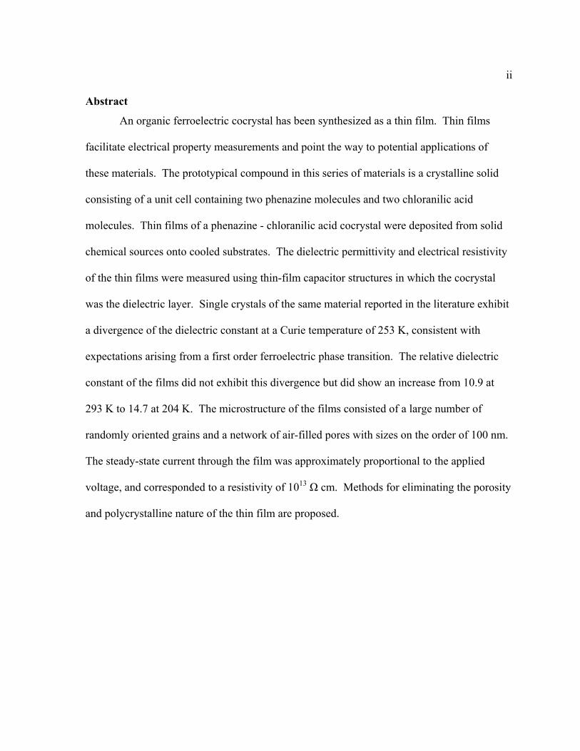
An organic ferroelectric cocrystal has been synthesized as a thin film. Thin films
facilitate electrical property measurements and point the way to potential applications of
these materials. The prototypical compound in this series of materials is a crystalline solid
consisting of a unit cell containing two phenazine molecules and two chloranilic acid
molecules. Thin films of a phenazine - chloranilic acid cocrystal were deposited from solid
chemical sources onto cooled substrates. The dielectric permittivity and electrical resistivity
of the thin films were measured using thin-film capacitor structures in which the cocrystal
was the dielectric layer. Single crystals of the same material reported in the literature exhibit
a divergence of the dielectric constant at a Curie temperature of 253 K, consistent with
expectations arising from a first order ferroelectric phase transition. The relative dielectric
constant of the films did not exhibit this divergence but did show an increase from 10.9 at
293 K to 14.7 at 204 K. The microstructure of the films consisted of a large number of
randomly oriented grains and a network of air-filled pores with sizes on the order of 100 nm.
The steady-state current through the film was approximately proportional to the applied
voltage, and corresponded to a resistivity of 1013 Ω cm. Methods for eliminating the porosity
and polycrystalline nature of the thin film are proposed.
iii Acknowledgements
Nicholas Thompson deserves the most appreciation and gratitude. Without Nick, this
work would not have been possible and may never have begun. Nick built the original
growth chamber, assisted with most experiments, and is solely responsible for all of the
scanning electron micrographs. Josef Spalenka deserves great thanks for depositing the
metals films used as contacts for the ferroelectric layers. Soonjoo Seo was incredibly helpful
with the development and maintenance of our vacuum chamber. Roberto Cruz was a
wonderful assistance during his short time with the group; his enthusiasm and dedication was
always above and beyond all of our expectations. I would also like to thank all of the other
members of the Paul Evans Research group not already specifically mentioned for their
comments, suggestions, and support. Lastly, and most importantly, I wish to thank Professor
Paul G. Evans who I have had the pleasure of working with for the past two and a half years.
His guidance, patience, and assistance have been invaluable. Without Prof. Evans more than
just this research and thesis would not have been possible or realized.
1
1. Introduction
Organic electronic materials including semiconductors, dielectrics, and conducting
polymers are an emerging class of materials with applications that are similar to their
inorganic counterparts.[1-3] The ease of processing organic molecules offers distinct
advantages in terms of cost and also offers a great degree of flexibility in integrating
electronic materials with a wide range of substrates.[1,4-5] In addition, organic electronic
materials offer functions that are not available in inorganic semiconductors, and have the
potential to allow these functions to be integrated in easily processed devices.[1,4,6]
Among the properties that are available in organic materials is ferroelectricity.
Organic ferroelectrics have properties that are similar to inorganic ferroelectrics, but with
much greater potential ease of integration. Although inorganic ferroelectrics are now
beginning to be integrated with silicon and other inorganic semiconductors, for example
SrTiO3 on Si, comprehensive materials integration is difficult because of the high
temperatures required to form the required metal oxides.[7] The chemical stability and low
processing temperatures of organic ferroelectrics promises to allow much more
straightforward integration.
Among the most promising of the organic ferroelectric materials are two-component
crystals formed from hydrogen donor and acceptor molecules. Horiuchi et al. have
discovered a class of organic crystals composed of two molecules connected by hydrogen
bonds to form a cocrystal.[8] These cocrystals have a first-order ferroelectric phase
transition, high dielectric permittivity, and high resistivity.[8-11] The electrical properties of
the cocrystals suggest applications as gate dielectric and ferroelectric layers in organic field
2 effect transistors (FETs).[9,12-13] This thesis describes efforts to develop and characterize
thin films of the two-component organic ferroelectrics.
1.1 Motivation
Ferroelectric materials offer several opportunities when used in electronic devices.
At the level of electronic components, ferroelectrics can be used to create non-volatile
memory elements and high dielectric constant layers. From a more fundamental perspective,
our interest in these materials arise from possible first-order phase transitions which can lead
to very high dielectric constants as described by the Curie-Weiss law.[14]
Since the dielectric constant of a ferroelectric with a first-order phase transition is
largest when the temperature is near the Curie temperature, materials with phase transitions
near a device’s operating temperature need to be selected. In comparison with other
materials, the ferroelectric phase transition of the cocrystals are found at temperatures which
are more practical for device applications.[8-11] The most commonly studied ferroelectric
cocrystal in this class, consisting of phenazine and chloranilic acid molecules, has a Curie
temperature of 253 K.[8,10,12-13,15-20] The names of these molecules are often
abbreviated as Phz and H2ca, respectively. Cocrystals or tricrystals (three-component
crystals) of an anilic acid (two anilic acid species in the case of tricrystals) and phenazine or
bipyridine have also been reported.[8,11] The deuteration of the anilic acid, for example to
create D2ca/Phz cocrystals, leads to an increase in the Curie temperature.[10] The origin of
this effect has not yet been definitively determined, but has been recently discussed by Koval
et al. as a change in the tunneling frequency due to the increased mass of the hydrogen and a
change in the geometry of the hydrogen bond.[21] Curie temperatures of the cocrystals and
3 tricrystals, and their deuterated analogs, can span a range between 140 K, for phenazine and
bromanilic acid cocrystals, to 335 K, for deuterated iodanilic acid and 5,5’-dimethyl-2,2’-
bipyridine (55DMBP).[8,11] The Curie temperature thus lies in a useful range of
temperatures for electronic devices. The transition temperatures and a number of other
properties are shown for several cocrystal compounds in Table 1.
Studying the cocrystals as thin films is important because integration of these
materials into devices will require the creation of flat planar layers. Thin films can be
integrated into devices such as thin-film capacitors, memories, and field effect transistors.
Films can also simplify studies of the electrical properties because the layers allow the
creation of wide, thin samples that are easily described mathematically. Additionally, it is
important to study the cocrystals as thin films if they are to be used in this way since this
form could change the material’s properties because of stresses or microstructures unique to
the thin film form. Thin films of the cocrystal have not been reported in the literature. To
date only articles describing single crystals and powders are published.[8,10,15,20]
The high dielectric constant and high resistivity of the cocrystals suggest that these
materials could be used as gate insulating layers in FETs. Increasing the dielectric constant
of the gate insulator increases the accumulated charge at the semiconductor-insulator
interface and thereby increases the channel conductivity.[22] The dielectric constant, at
room temperature and the Curie temperature, of several cocrystal compounds are listed in
Table 1. Improving the resistivity of the gate dielectric reduces the leakage currents to the
gate.
4 The low coercive fields and moderate spontaneous polarization of organic
ferroelectrics may allow the cocrystals to act as the ferroelectric layers in ferroelectric FETs
(FeFETs).[ 23] In FeFETs the dielectric constant and resistivity of the ferroelectric layer are
equally important as in the FETs, but the ferroelectric properties of the layer become
essential as well. The polarization of the ferroelectric can act as an effective gate voltage in
addition to the externally supplied bias and thereby alter the magnitude of the source-drain
current. By measuring the source-drain current for a constant gate voltage the state of the
polarization can be inferred.[23] These characteristics allow FeFETs to act as non-volatile
memories in which the state of the memory is read without destroying the stored
information.[23] The relevant properties of the ferroelectric layers are the coercive electric
field and the spontaneous polarization. The coercive field is the electric field necessary to
switch the state of the polarization. The spontaneous polarization is the average electric
dipole moment per unit volume of the crystal. Small coercive fields allow for lower
operating voltages. Large polarizations increase the effective gate voltage. The values of
these properties may vary with the composition of the ferroelectric (Table 1).
1.2 Goals
Our goal was to create thin films of a prototypical compound in this class to study
their electronic properties. We have investigated the growth of the hydrogen bonded organic
thin films, searched for the ferroelectric phase transition in thin films, and studied electronic
transport through the films using resistivity measurements. These studies attempted to
determine the necessary growth conditions of cocrystal films for use in FETs and FeFETs.
Our research has documented the dielectric constant as a function of temperature and
5 resistivity of the films. Future experiments will attempt to integrate these materials into
device structures.
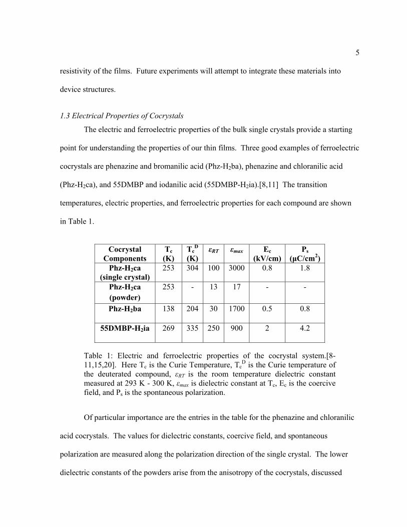
1.3 Electrical Properties of Cocrystals
The electric and ferroelectric properties of the bulk single crystals provide a starting
point for understanding the properties of our thin films. Three good examples of ferroelectric
cocrystals are phenazine and bromanilic acid (Phz-H2ba), phenazine and chloranilic acid
(Phz-H2ca), and 55DMBP and iodanilic acid (55DMBP-H2ia).[8,11] The transition
temperatures, electric properties, and ferroelectric properties for each compound are shown
in Table 1.
Cocrystal
Components Tc
(K) Tc
D
(K) εRT εmax Ec
(kV/cm)Ps
(μC/cm2) Phz-H2ca
(single crystal) 253 304 100 3000 0.8 1.8
Phz-H2ca (powder)
253 - 13 17 - -
Phz-H2ba 138 204 30 1700 0.5 0.8
55DMBP-H2ia 269 335 250 900 2 4.2
Table 1: Electric and ferroelectric properties of the cocrystal system.[8-11,15,20]. Here Tc is the Curie Temperature, Tc
D is the Curie temperature of the deuterated compound, εRT is the room temperature dielectric constant measured at 293 K - 300 K, εmax is dielectric constant at Tc, Ec is the coercive field, and Ps is the spontaneous polarization.
Of particular importance are the entries in the table for the phenazine and chloranilic
acid cocrystals. The values for dielectric constants, coercive field, and spontaneous
polarization are measured along the polarization direction of the single crystal. The lower
dielectric constants of the powders arise from the anisotropy of the cocrystals, discussed
6 below in Section 2.3. The dielectric constant of the powders increases at the Curie
temperature, but the effect is not as pronounced as it is for the single crystals.[8,16]
The range of electrical properties of the ferroelectric cocrystals is exemplified by the
four materials listed in Table 1. Properties outside of the ranges shown in Table 1 may
become possible in the future by developing new compounds with different molecular
components. As more molecular components which are capable of forming a ferroelectric
cocrystal are discovered the range of these properties may expand. The discovery of new
components and compounds is an area of active research.[24]
1.4 Comparison with Ferroelectric Polymers
Ferroelectric polymers comprise a second important class of organic ferroelectric
materials.[25-30] The electric and ferroelectric properties of the polymer are a benchmark
for the cocrystals, especially since the two classes of materials have similar potential
applications. Polyvinylidene fluoride (PVDF) and a copolymer of PVDF with
trifluoroethylene (P(VDF-TrFE)) are the most important and widely studied ferroelectric
polymers.[25-29,31-33] Ferroelectric polymers have been used as the gate dielectric or
ferroelectric layer in FETs and memories.[25-30]
Like the cocrystals, the ferroelectric properties of the polymers are a result of their
chemical and crystalline structure. The VDF oligomer is responsible for the ferroelectric
properties of PVDF and P(VDF-TrFE). The copolymer is used to stabilize the material in the
ferroelectric phase.[25] The ferroelectric properties of the polymer are due to the dipole
moments between the hydrogen and fluorine atoms bonded to the carbon backbone. In order
for the dipoles to align, a rotation around the carbon chain is required of the fluorine and
7 hydrogen atoms. This rotation requires a considerable amount of energy, and results in large
coercive fields, up to 500 kV/cm.[32] The spontaneous polarization is 13 μC/cm2.[33] Both
of these values are larger than the values for the cocrystal ferroelectrics as shown in Table 1.
The large polarization allow the films to perform well in FeFETs.[29-30,34-35] Work is
being done to reduce the coercive field.[36-37]
Unlike cocrystals, ferroelectric polymers lack a first order phase transition. It has
been predicted that the Curie temperature of the polymers is above its glass transition
temperature.[25] The divergence of the dielectric constant is not apparent in electrical
measurements because the ferroelectric phase vanishes at the glass transition.[23]
The dielectric susceptibilities of ferroelectric polymers range from 9 to 25 depending
on the composition of the copolymer.[25-28] The resistivity of ferroelectric polymers is
high, on the order of 1012 Ω cm - 1014 Ω cm.[25-28] The resistivity does not reach values for
inorganic insulators such as SiO2, 1014 Ω cm – 1016 Ω cm, which is one of the most
commonly used dielectrics in electronic devices.[22]
8 2. Structural and Electrical Properties
The electrical properties of the cocrystal are a result of its crystal structure. The most
notable feature of the cocrystal structure is the hydrogen bond between phenazine and
chloranilic acid molecules. The hydrogen bond is also the origin of the crystal’s ferroelectric
properties so a brief discussion of the bond and its relation to the phase transition is provided.
2.1 Structure of Phenazine and Chloranilic Molecules
The chemical structure of the pure phenazine and chloranilic acid compounds provide
insight into the formation of the cocrystal. Chloranilic acid has a single monoclinic
crystalline phase (a = 10.03 Å, b = 5.544 Å, c = 7.566 Å, β = 104.8o).[38] Phenazine has two
crystalline polymorphs.[39-40] The more relevant of these phases for our work was the
monoclinic β-phase (a = 11.64 Å, b = 11.54 Å, c = 6.898 Å, β = 99.48o).[39-40] The
structures of phenazine and chloranilic acid molecules are shown in Figure 1. Chloranilic
acid has two -OH groups on opposite sides of the molecule.[38] Each of these groups can
participate in a hydrogen bond with other molecules. Chloranilic acid is a hydrogen donor
(D) since it can provide protons in the hydrogen bonds. Phenazine has two nitrogen atoms
on opposite sides of the molecule, each of which is capable of participating in a hydrogen
bond.[39-40] Phenazine is a hydrogen acceptor (A) since protons can bind to the nitrogen
atoms. The ability for these two chemicals to form two hydrogen bonds on opposite sides of
the molecule is the basis for the structure of the cocrystal and is generally true for the
cocrystal material system.[9,11-13,16,18]

9
Figure 1: Chemical structure sketch of the two molecules composing the cocrystal.
2.2 Structure of Phenazine-Chloranilic Cocrystals
The structure of the phenazine and chloranilic acid cocrystal has been determined by
Horiuchi et al.[8,10] When phenazine and chloranilic acid molecules cocrystallize each
molecule forms two hydrogen bonds to form semi-infinite chains with a …DADA… pattern.
These chains run along the [110] and [1-10] crystallographic directions.[8,17] The chains of
molecules pack together into planes parallel to the (001) plane.[10] Similarly oriented chains
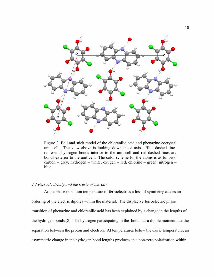
stack along the [001] direction with alternating chain orientations.[10] The unit cell of the
cocrystal is monoclinic with lattice constants of a = 12.43 Å, b = 3.80 Å, c = 16.92 Å, and
angle β = 107.8o.[10] A schematic diagram of the crystal structure viewed along the b-axis is
shown in Figure 2. The physical arrangement and hydrogen bonds of the molecules within
the unit cells are responsible for the ferroelectric and dielectric properties of the material.
O
O
Cl
Cl
OH
OH
N
N
Chloranilic Acid Phenazine
10
Figure 2: Ball and stick model of the chloranilic acid and phenazine cocrystal unit cell. The view above is looking down the b axis. Blue dashed lines represent hydrogen bonds interior to the unit cell and red dashed lines are bonds exterior to the unit cell. The color scheme for the atoms is as follows: carbon – grey, hydrogen – white, oxygen – red, chlorine – green, nitrogen – blue.
2.3 Ferroelectricity and the Curie-Weiss Law
At the phase transition temperature of ferroelectrics a loss of symmetry causes an
ordering of the electric dipoles within the material. The displacive ferroelectric phase
transition of phenazine and chloranilic acid has been explained by a change in the lengths of
the hydrogen bonds.[8] The hydrogen participating in the bond has a dipole moment due the
separation between the proton and electron. At temperatures below the Curie temperature, an
asymmetric change in the hydrogen bond lengths produces in a non-zero polarization within
11 the unit cell.[8] The dipole moment of each unit cell of the cocrystal is determined by the
length and symmetry of the hydrogen bonds. Above the Curie temperature, all of the
hydrogen bonds have equal lengths and the net dipole moment is zero. Below the Curie
temperature displacements of the phenazine and chloranilic acid molecules by less than 10
pm cause the length of the hydrogen bond on one side of the molecule (either phenazine or
chloranilic acid) to become longer than the other.[10] This asymmetry give rise to a net
polarization along the b axis of the unit cell.[8]
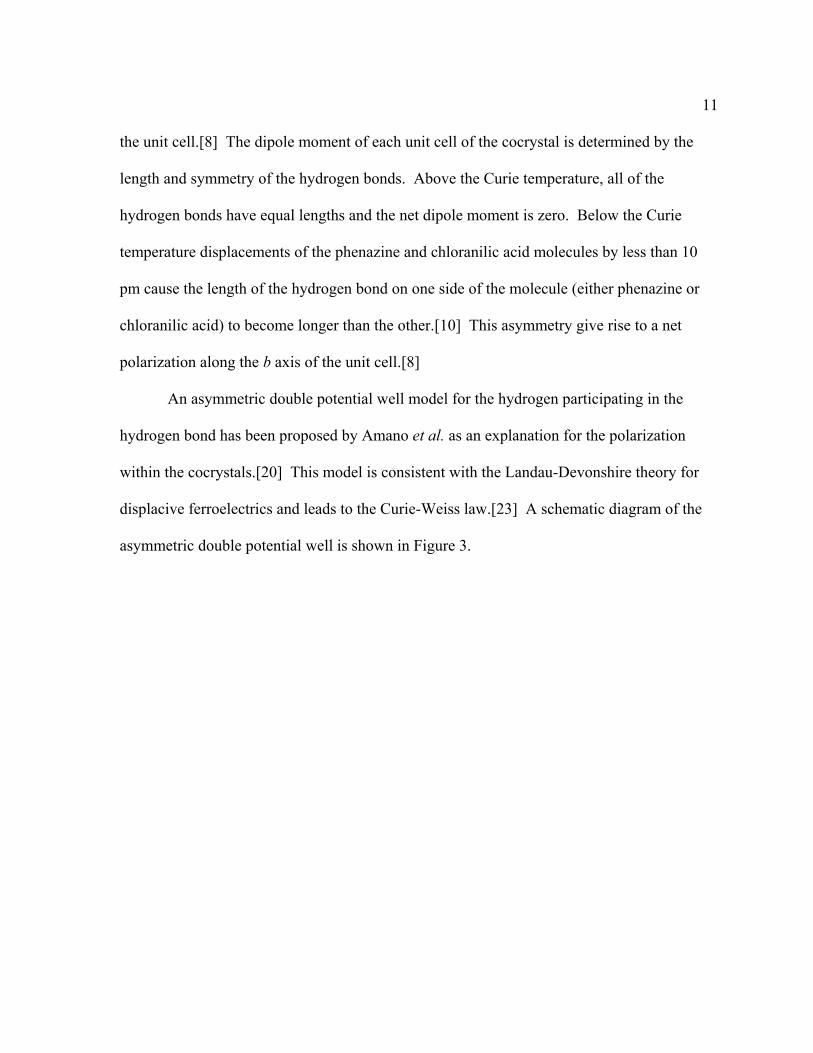
An asymmetric double potential well model for the hydrogen participating in the
hydrogen bond has been proposed by Amano et al. as an explanation for the polarization
within the cocrystals.[20] This model is consistent with the Landau-Devonshire theory for
displacive ferroelectrics and leads to the Curie-Weiss law.[23] A schematic diagram of the
asymmetric double potential well is shown in Figure 3.
12
Figure 3: Schematic diagram of the free energy double potential well for the chloranilic acid and phenazine cocrystal proposed by Amano et al.[20] Arrows indicate the dipole moment of the hydrogen bonds which are themselves represented as the dashed lines. Protons participating in the hydrogen bonds are shown in green. Drawing is adopted from ref. 20.
The divergence in the dielectric constant of phenazine and chloranilic acid cocrystals
can be explained by the Curie-Weiss law. The first order phase transition is due to the
evolution of the free energy as a function of temperature. As the temperature is increased
from below the Curie temperature the double potential well suddenly becomes a single well,
as shown in Figure 3. This sudden loss of a second well causes the proton to settle into the
only available well. Therefore, the previously aligned dipole moments now cancel and the
Phz Phz Phz PhzH2ca H2ca H2ca
Phz Phz Phz PhzH2ca H2ca H2ca
Paraelectric phase, T > Tc
Ferroelectric phase, T < Tc
13 net polarization is lost. This sudden change in the polarization causes a divergence in the
dielectric constant near the transition temperature.
The dielectric constant does not go to infinity but can increase by one or more orders
of magnitude. The dielectric constant of the phenazine and chloranilic acid cocrystal can
increase from 100 at room temperature to 3000 at the Curie temperature.[8] This is the
largest divergence reported for any organic ferroelectric.[12]
The dielectric permittivity of the cocrystal depends on the orientation between the
external electric field and the crystal planes. The largest dielectric permittivity is observed
when the external electric field is aligned parallel to the b-axis, the polarization direction, of
the cocrystal. The electrical properties for this crystal direction are listed in Table 1 as the
single crystal values.
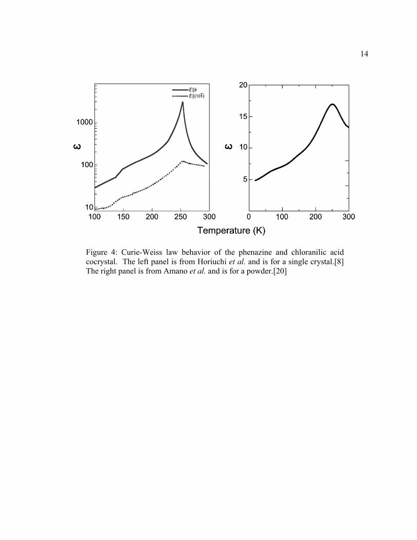
Two previous studies have reported the temperature dependence of the dielectric
constant of phenazine and chloranilic acid cocrystal. Horiuchi et al. measured the dielectric
constant as a function of temperature, along the polarization direction [010], and along a
perpendicular direction, [10-1], to demonstrate the anisotropy of the crystals.[8] The left
panel of Figure 4 shows the expected sharp divergence of the dielectric constant at the Curie
temperature. Amano et al. made the same measurement of a powder of the cocrystal sample
and a plot of their data is shown in the right panel of Figure 4.[20] Amano et al. found an
increase of the dielectric constant at the Curie temperature but did not observe the sharp
divergence found by Horiuchi et al.[8,20] The magnitude of the dielectric constant of the
powders is less than the magnitude measured for the single crystal and the effect has been
attributed to the anisotropy of the cocrystal.[20]
14
Figure 4: Curie-Weiss law behavior of the phenazine and chloranilic acid cocrystal. The left panel is from Horiuchi et al. and is for a single crystal.[8] The right panel is from Amano et al. and is for a powder.[20]

15 3. Thin Film Growth and Structural Properties
A physical vapor deposition system using vacuum sublimation and condensation was
used to grow the cocrystal thin films from pure chemical powder sources. Films were
characterized structurally using x-ray diffraction to determine what crystalline structures
were present in the films. Scanning electron microscopy (SEM) was used to determine the
morphology of the films. Film thicknesses were measured optically with a non-contact
profilometer and these measurements were confirmed by SEM images.
3.1 Thin Film Growth Vacuum Chamber
We designed and built a vacuum chamber to deposit the cocrystal films. By using our
own design we were able to modify the system to control various growth parameters such as
source temperatures and fluxes, and substrates temperatures. The chamber included two
effusion cells for the chemical sources. A photograph of the chamber is shown in Figure 5.
Figure 5: Photographs of the chamber (left) and substrate stage (right). The photograph of the chamber is taken from above. The substrate stage is shown connected to the vacuum chamber as the flange closest to the bottom of the left image. In the right image the substrate stage has been removed from the chamber to show the details of the apparatus.
16 Two pumps were used to evacuate the chamber. Vacuum in the chamber was
maintained with a continuously operating turbomolecular pump (TMP) separated from the
main chamber by a gate valve. A sorption pump was used in the initial reduction of the
pressure from one atmosphere to 10-4 torr. Opening the gate valve allowed the TMP to
further reduce the pressure to 10-8 torr after eight to ten hours. The pressure in the chamber
was monitored with an ion gauge.
Two chemical effusion cells were used to sublimate solid chemical sources. The
effusion cells were placed in line of sight of the substrate. Chemical source powders were
purchased from Sigma-Aldrich (St. Louis, MO). The chloranilic acid purity was 100.2% as
determined by titration with sodium hydroxide and the phenazine purity was 98%. These
purities were determined by the manufacturer. The effusion cells were independently heated
by tungsten filaments. The temperatures of the effusion cells were measured using type-K
thermocouples cemented to the end of the quartz crucibles containing the precursor materials.
Each effusion cell was also equipped with a rotatable shutter.
The temperature of the effusion cells produced by the filament was not reliable. It
appeared that the temperature was dependent on the amount of source powder placed into the
cell. Due to this difficulty the temperature of the effusion cells would vary by 3 K to 5 K for
a particular current. Fortunately, these small fluctuations did not appear to affect the results
of film growth by an observable amount.
3.2 Thin Film Growth
The substrates for the thin films were mounted on a cooling stage for the deposition
(Figure 5). Films would not form on room temperature substrates so the growth procedure
17 always began by cooling the substrate stage to between 110 K and 140 K with a liquid
nitrogen bath. The liquid nitrogen was contained in a Styrofoam bucket on the outside of the
chamber and a thermal feed-through, consisting of two copper posts passing through a
vacuum flange, was used to make the connection between the substrate stage and the cooling
bath. The temperature of the stage was measured with a silicon diode (Lake Shore
Cryotronics, Westerville, OH, model DT-470-SD-12).
The sublimation of the powder sources began after the substrates were completely
cooled. Once the temperature of the substrates was below 140 K heating of the effusion cells
began with the shutters closed. The chloranilic acid powder was heated to 93 oC and the
phenazine powder was heated to 70 oC. When the sources were heated the pressure in the
chamber increased from 10-8 torr to 10-6 torr. Growth at these pressures takes advantage of
the molecular transport properties of the vacuum due to the low number of scattering events
during the time-of-flight between the effusion cells and substrates. Once the chemical
sources reached the specified temperatures, the shutters were opened to start the deposition
process.
A range of different deposition times were used for the growth of the thin films. The
durations of the deposition ranged from 40 minutes to four hours. The most common
duration was one hour. The thickness of the films depended on the deposition time and the
source flux (a function of the source temperature). The thickness of the film was controlled
by the duration of the deposition time.
The sublimation and film growth process was stopped after the deposition duration
elapsed. At the end of the deposition time the cooling of the substrates was halted, the
18 shutters were closed, and the heaters were turned off. Once the substrates had returned to
room temperature, they were removed from the vacuum chamber.
3.3 Experimental Device Structure
Figure 6 shows a schematic diagram of the capacitor structure. The Au metal films
used for bottom electrodes were deposited by electron-beam evaporation onto Si substrate.
These metal films were used as the bottom electrode in the thin film capacitor structure. A
second set of substrates used Ni instead of Au in the bottom electrode in order to investigate
any changes in the growth of the films on different surfaces. The cocrystal films were
deposited onto the metal films using the vacuum sublimation process described in Section
3.2.
The final step to create the capacitor structures was to deposit the top electrodes.
These electrodes were deposited by electron-beam evaporation. The size of the electrodes
was defined by a shadow mask placed on top of the film. These electrodes were circular
pads between 170 μm and 190 μm in diameter.
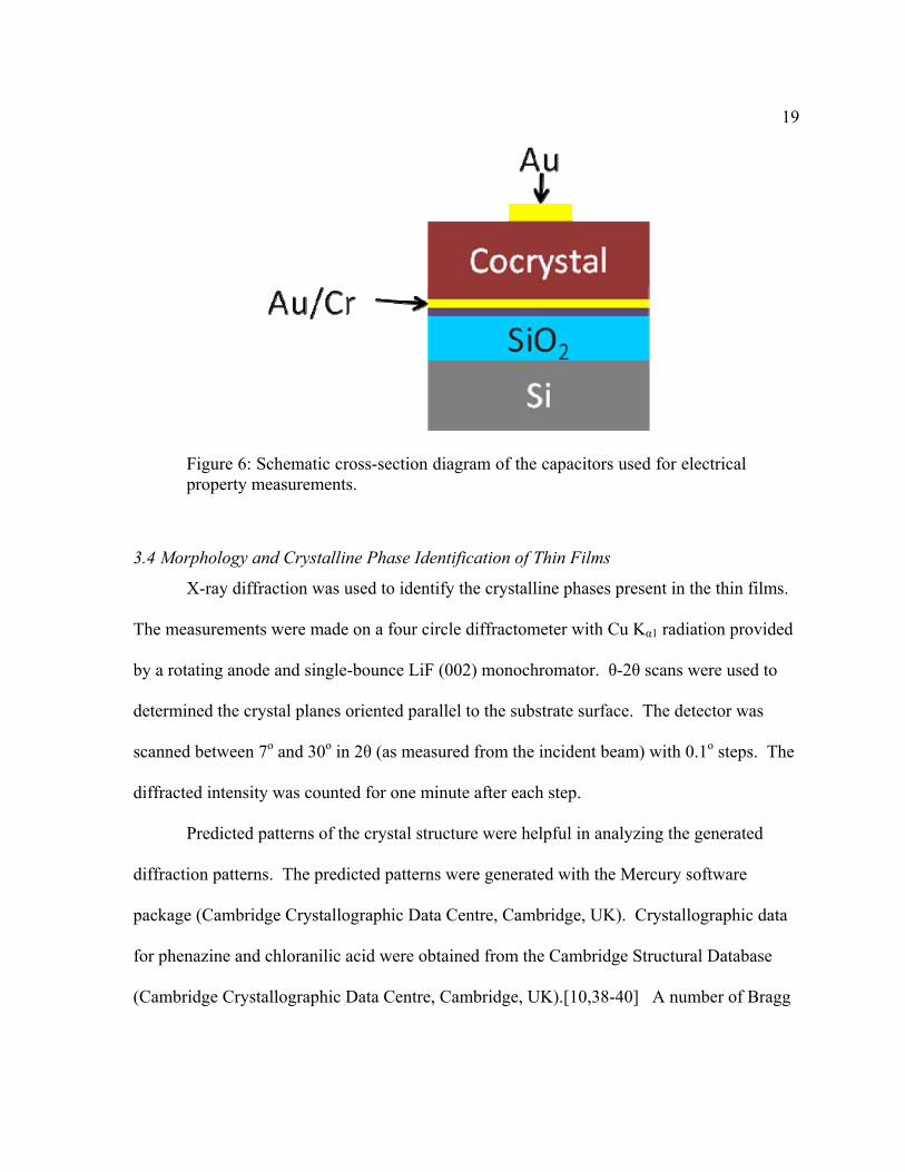
19
Figure 6: Schematic cross-section diagram of the capacitors used for electrical property measurements.
3.4 Morphology and Crystalline Phase Identification of Thin Films
X-ray diffraction was used to identify the crystalline phases present in the thin films.
The measurements were made on a four circle diffractometer with Cu Kα1 radiation provided
by a rotating anode and single-bounce LiF (002) monochromator. θ-2θ scans were used to
determined the crystal planes oriented parallel to the substrate surface. The detector was
scanned between 7o and 30o in 2θ (as measured from the incident beam) with 0.1o steps. The
diffracted intensity was counted for one minute after each step.
Predicted patterns of the crystal structure were helpful in analyzing the generated
diffraction patterns. The predicted patterns were generated with the Mercury software
package (Cambridge Crystallographic Data Centre, Cambridge, UK). Crystallographic data
for phenazine and chloranilic acid were obtained from the Cambridge Structural Database
(Cambridge Crystallographic Data Centre, Cambridge, UK).[10,38-40] A number of Bragg
20 reflections that proved useful in differentiating the phases fell between ten and thirty degrees
in two-theta at the Cu Kα1 photon energy.
Experimentally generated patterns were compared with the predicted patterns to
indentify which crystalline phases were present in the films. This method allowed us to
indentify all known phases of phenazine, chloranilic acid, and their cocrystal; mixtures of
these phases could also be identified in this way. The diffraction experiments allowed us to
use only films which were the cocrystal for the electrical property measurements. Films
containing observable amounts of phenazine or chloranilic acid crystal phases were not used
for the electrical measurements.
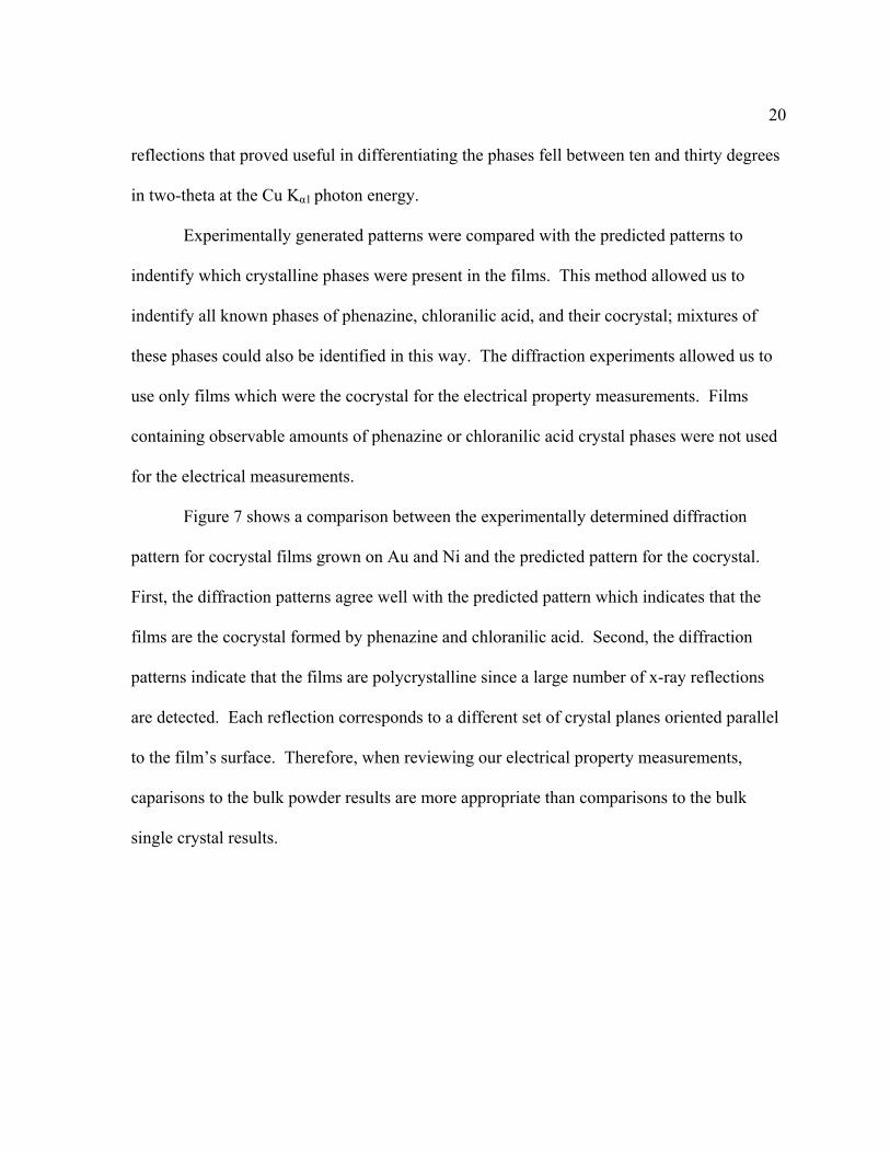
Figure 7 shows a comparison between the experimentally determined diffraction
pattern for cocrystal films grown on Au and Ni and the predicted pattern for the cocrystal.
First, the diffraction patterns agree well with the predicted pattern which indicates that the
films are the cocrystal formed by phenazine and chloranilic acid. Second, the diffraction
patterns indicate that the films are polycrystalline since a large number of x-ray reflections
are detected. Each reflection corresponds to a different set of crystal planes oriented parallel
to the film’s surface. Therefore, when reviewing our electrical property measurements,
caparisons to the bulk powder results are more appropriate than comparisons to the bulk
single crystal results.
21
Figure 7: Scattered intensity vs. 2θ (the angle between the incoming and diffracted beam). The top and bottom panels correspond to cocrystal films grown on Au and Ni, respectively. The predicted diffraction pattern is provided for comparison and is shown in grey in each panel. These diffraction patterns indicate that both films are the cocrystal and are polycrystalline.
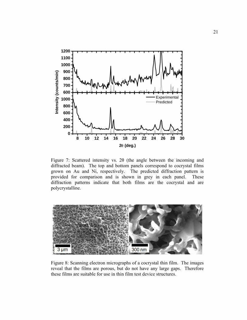
Figure 8: Scanning electron micrographs of a cocrystal thin film. The images reveal that the films are porous, but do not have any large gaps. Therefore these films are suitable for use in thin film test device structures.
600
700
800
900
1000
1100
1200
Experimental Predicted
Inte
nsi
ty (
co
un
ts/m
in)
8 10 12 14 16 18 20 22 24 26 28 300
200
400
600
800
1000
2 (deg.)
22 Scanning electron microscopy was used to view the morphology of cocrystal thin
films. SEM images of the cocrystal are shown in Figure 8. The images reveal that the film
structure is porous. The pores are on the order of 100 nm and do not penetrate directly to the
substrate. Electrodes deposited on top of these films would not be electrically shorted to the
bottom electrode. The porosity of the film needs to be considered when interpreting the
electrical property measurements because effects such as the high surface area, low dielectric
constant voids, possible surface conductivity, surface tension, and stresses could affect our
results.
The thickness of the films was determined using three different experimental
techniques since it was difficult to accurately measure the thickness with any individual
method. During film growth a portion of the substrate was shadowed with a glass cover slip
to provide a step-edge. First, SEM images taken at oblique angles (nearly parallel to the
substrate’s surface) were used to measure the height of the step-edge. A second, but similar,
technique on cleaved substrates allowed for measurement of the film’s thickness at an
interior point of the film. The third method used an optical profilometer to measure the
height of the step-edge. It was found that the profilometer had difficulty imaging the height
of the as-grown edge, but sputtering of a thin film of Au across the edge allowed for reliable
measurements. All three techniques agreed on the thickness of a particular film to within
10%. Although the thickness of a film was different for each growth, all thicknesses were
between one and two microns.
23 4. Dielectric Constant and Resistivity of Cocrystal Thin Films
The dielectric constant as a function of temperature and the electrical resistivity of the
thin films were measured. The dielectric constant measurements were made to determine
whether the cocrystals exhibit Curie-Weiss behavior. A large number of capacitors were
measured at room temperature to do a statistical study of the dielectric constant. To our
knowledge, no precise measurements of the resistivity of the cocrystals have been
published.[8] By measuring the current-voltage relationship of the capacitor devices we have
calculated the resistivity of the films.
4.1 Low Temperature Dielectric Constant Measurements
The temperature dependence of the dielectric constant can be used to study the
ferroelectricity of the cocrystal. Since the Curie temperature of bulk single crystals is 253 K,
measurements were made in vacuum and used a cryostat to control the temperature during
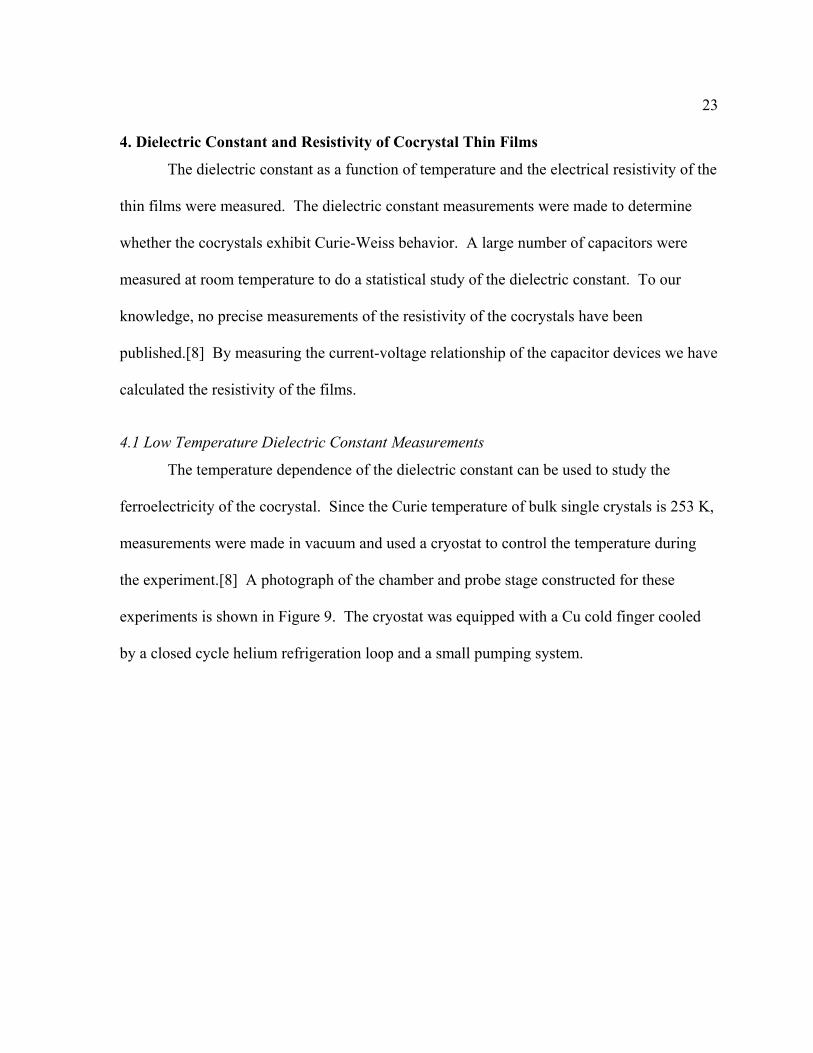
the experiment.[8] A photograph of the chamber and probe stage constructed for these
experiments is shown in Figure 9. The cryostat was equipped with a Cu cold finger cooled
by a closed cycle helium refrigeration loop and a small pumping system.
24
Figure 9: Photograph of the cryostat (left) and probe stage (right). The photograph of the cryostat also shows the motion stage and microscope. Pictured in the right photograph is one of cocrystal films, light brown rectangle slightly right and up from center.
The cryostat was constructed with the capability to make precise measurements of the
small capacitance of our devices. An electrical feed-through was added for coaxial cables
which minimized the mutual capacitance between the test leads by grounding the outer
conductor of the wires. Connections from the center conductor of the coax wires to the test
devices were made with two very fine Pt wires, one soldered to the bottom electrode and the
second touching a top electrode.
The capacitance of the devices was measured with an Andeen-Hagerling 2500A
Capacitance Bridge at 1 KHz and a maximum of 0.75 volts rms. Measurements of the
temperature and capacitance were automatically recorded as the temperature was decreased
from 290 K - 320 K to 40 K - 100 K. After the temperature of the device stabilized at a
minimum, the refrigeration was stopped and the test device was allowed to warm slowly
while temperature and capacitance measurements were continued. We calculated the
25 dielectric constant from measurements of capacitance. The relationship between these values
is:
4
(1)
Here ε is the dielectric constant of the film, l is the distance between the electrodes, C is the
measured capacitance, εo is the permittivity of free space, and D is the diameter of the top
electrode. Equation (1) assumes that both conducting plates of the capacitor are circular and
parallel. Therefore this equation is an approximation for the devices tested since the bottom
electrode is not a circle of diameter D, but is nearly infinite on the scale of the top electrode.
Additionally, Equation (1) assumes that the dielectric medium is continuous and isotropic, so
the calculated value of ε using this equation will be the effective dielectric constant for the
section of polycrystalline, porous film between the electrodes.
4.2 Analysis of Low Temperature Measurements
The relationship between the temperature and dielectric constant of the thin films is
compared to the same relationship for bulk single crystals and powders. The differences
between the temperature and dielectric constant relationships of single crystals, powders, and
films can be explained by a discussion of their structure and the anisotropy of the crystal.
Recall the discussion of the effects of crystal anisotropy from Section 2.3.
We measured the dielectric constant of the thin films as a function of temperature.
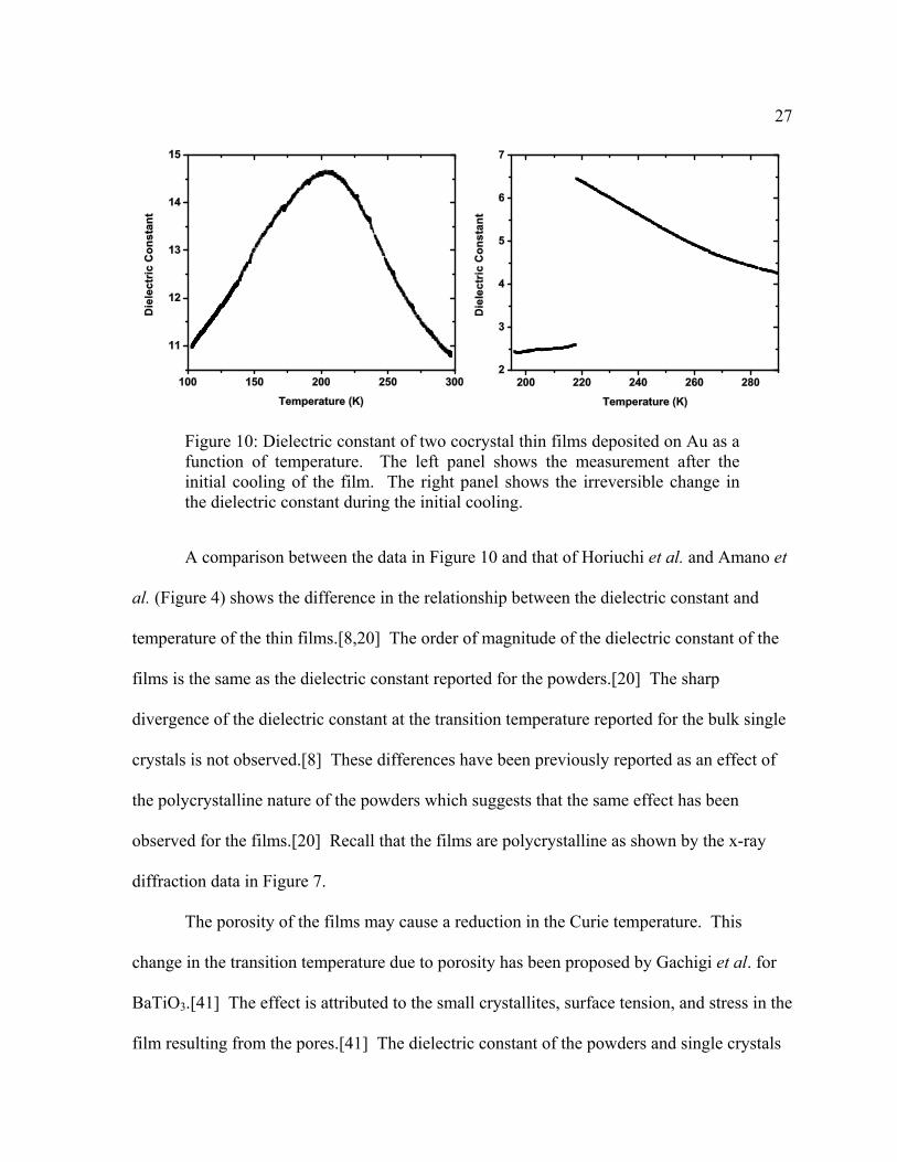
Our results are shown in the left panel of Figure 10. The dielectric constant at room
temperature was 10.9 and as the temperature decreased the dielectric constant increased to
14.7 at 204 K. Below this temperature the dielectric constant decreased to 10.9 at 103 K,
26 which was the lowest temperature of our measurements. Note that the maximum dielectric
constant did not occur at the Curie temperature of the bulk single crystals. Since the
maximum dielectric constant for both the single crystal and powder is observed at the same
temperature our results suggest an effect, such as a reduction of the Curie temperature, which
is unique to the thin film form.
During our experiments we observed an effect which will be important for future
experiments. The measurements in the left panel of Figure 10 were taken while warming the
film after the first time it had been cooled. Data from another film (right panel of Figure 10)
suggests an irreversible change takes place during the initial decrease in temperature. The
dielectric constant decreases discontinuously at 218 K, but does not have the same
discontinuity while the film is returning to room temperature. Inspection of the film with
SEM reveals the formation of cracks in the film. Future work will require more
mechanically stable capacitor structures to eliminate crack formation and artifacts associated
with irreversible structural changes.
27
Figure 10: Dielectric constant of two cocrystal thin films deposited on Au as a function of temperature. The left panel shows the measurement after the initial cooling of the film. The right panel shows the irreversible change in the dielectric constant during the initial cooling.
A comparison between the data in Figure 10 and that of Horiuchi et al. and Amano et
al. (Figure 4) shows the difference in the relationship between the dielectric constant and
temperature of the thin films.[8,20] The order of magnitude of the dielectric constant of the
films is the same as the dielectric constant reported for the powders.[20] The sharp
divergence of the dielectric constant at the transition temperature reported for the bulk single
crystals is not observed.[8] These differences have been previously reported as an effect of
the polycrystalline nature of the powders which suggests that the same effect has been
observed for the films.[20] Recall that the films are polycrystalline as shown by the x-ray
diffraction data in Figure 7.
The porosity of the films may cause a reduction in the Curie temperature. This
change in the transition temperature due to porosity has been proposed by Gachigi et al. for
BaTiO3.[41] The effect is attributed to the small crystallites, surface tension, and stress in the
film resulting from the pores.[41] The dielectric constant of the powders and single crystals
28 would not experience this change in the Curie temperature since the porous structure is found
only in the thin films. Future experiments may be able to determine the validity of this
conclusion if non-porous films can be grown.
4.3 Room Temperature Statistical Study
We measured a large number of devices at room temperature in a statistical study of
the dielectric constant of cocrystal ferroelectric thin films. For this study the uncertainty in
each measured value was determined. The measured properties which could affect the
calculated dielectric constant are film thickness, top electrode diameter, and capacitance as
shown in Equation (1).
The capacitance and dimensions of two cocrystal films were measured for the
statistical study. One of the films was grown on an Au bottom electrode and the other on Ni
bottom electrode. Thirty devices with Au contacts and twenty devices with Ni contacts were
measured for each film. The capacitance of a device was determined as the difference
between the capacitance of a device minus the capacitance just before electrical contact to the
top electrode was made. The thickness of the film was measured five times with the optical
profilometer and the average of these measurements was used for the calculations. The
diameter of multiple electrodes on each film was measured with SEM images and the
average of these values was used in the calculations. Equation (1) was used to calculate the
dielectric constant of the measured devices.
A distribution of dielectric constants was found due to systematic and experimental
errors in the measurements of the capacitance, film thickness, and top electrode diameter. To
characterize this error the standard deviation of each measured variable was estimated, the
29 error was propagated through the calculation, and the uncertainty of the dielectric constant
calculations was determined.
Three different procedures where used to estimate the standard deviation of the
variables in Equation (1). The capacitance bridge would display the measured capacitance
continually. During our measurements, the first several digits would remain constant and the
fourth or fifth digit would fluctuate. The standard deviation of the capacitance was estimated
as being one order of magnitude greater than the order of the fluctuating digit, which was on
the order of 10-2 pF. The uncertainty in the measurement of thickness was estimated as one
standard deviation from the average, 300 nm. The uncertainty in the top electrodes was
estimated as the largest difference from the average diameter, 10 μm. Estimating the
standard deviation of the diameter and capacitance as we did is likely an overestimate, but
since both were much less than the uncertainty in the film thickness the results were not
significantly affected. The relatively large uncertainty (10 % to 20% compared to less than
1% for the other values) in the film thickness measurements tended to dominate the
calculation of the total error.
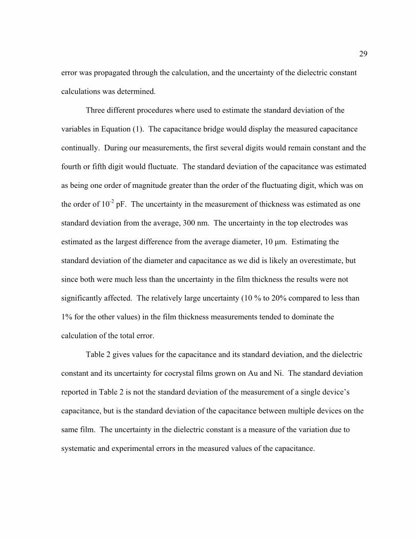
Table 2 gives values for the capacitance and its standard deviation, and the dielectric
constant and its uncertainty for cocrystal films grown on Au and Ni. The standard deviation
reported in Table 2 is not the standard deviation of the measurement of a single device’s
capacitance, but is the standard deviation of the capacitance between multiple devices on the
same film. The uncertainty in the dielectric constant is a measure of the variation due to
systematic and experimental errors in the measured values of the capacitance.
30
Bottom Electrode
Capacitance (pF) Dielectric Constant Average Std. Deviation Average Uncertainty
Au 1.61 0.171 12.9 1.37
Ni 3.62 0.283 13.1 1.02
Table 2: Room temperature measurements of two cocrystal films grown on two species of bottom electrodes.
Two conclusions can be drawn from the data in Table 2. First, the dielectric constant
is statistically equivalent for the films grown on Au and Ni bottom electrodes. This indicates
that the different electrodes are not affecting the dielectric constant of the films. Second, the
dielectric constant of both of the films is equivalent to the bulk powder values reported by
Saito et al. and Amano et al.[15,20] Both of these reports have shown independently that the
room temperature dielectric constant of the phenazine and chloranilic acid cocrystals is
13.[15,20]
4.4 Resistivity of Cocrystal Thin Films
We calculated the electrical resistivity of our films from measurements of resistance.
The film’s resistivity is related to the experimentally observed resistance by using:
4
(2)
Here ρ is the resistivity, D is the device diameter, R is the measured resistance, and d is the
distance between the top and bottom electrodes. The resistance is computed from a
measurement of the steady-state current as a function of the applied voltage using Ohm’s
31 law. Data for resistivity measurements is presented as a plot of current versus voltage called
an IV curve.
Measurements of the steady-state current were made as a function of applied voltage.
These experiments used the capacitor structures described in Section 3.3. The measurements
were made using an Agilent 4155C Semiconductor Parameter Analyzer. Voltages were
scanned between -10 V and 10 V, in steps of 0.5 V, and the current was recorded after each
step. A pause of 20 seconds was observed between each voltage step and the corresponding
current measurement. Voltage scans were repeated with different voltage ranges and
directions to ensure that charging or discharging of the capacitor was not affecting the
measured current. This procedure ensured that the current passing through the capacitor had
reached the steady-state limit and not being affected by transient currents.
4.5 Analysis of Resistivity Measurements
Plots of the current flowing between the electrodes as a function of the applied
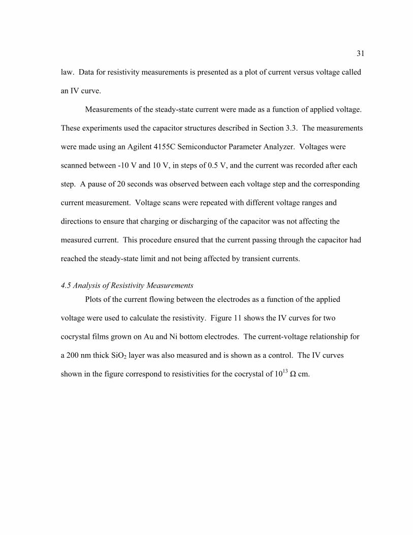
voltage were used to calculate the resistivity. Figure 11 shows the IV curves for two
cocrystal films grown on Au and Ni bottom electrodes. The current-voltage relationship for
a 200 nm thick SiO2 layer was also measured and is shown as a control. The IV curves
shown in the figure correspond to resistivities for the cocrystal of 1013 Ω cm.
32
Figure 11: Current-voltage curves for cocrystal films grown on Ni and Au respectively. The red line in each graph is the average linear fit of all three devices. The slope of this fit is proportional to the resistivity, 1013 Ω cm.
The electrical circuit which was used to make the meausrements of the data shown in
Figure 11 was designed to ensure accurate measurements of small currents. Since the
resistance of the capacitors was relatively high the current passing through the device was on
the order of 1 - 10 pA. Currents of the same magnitude can also be generated in the leads
from a variety of other effects such as vibrations in the wires, poor insulation on the wires, or
uninsulated soldered connections. To prevent these sources of error, only the center
conductors of coax wires were used for the electrical connections, all sheilding was
grounded, solder joints were insulated with shrink-wrap tubing, and vibration damping pads
were used to support the cables and equipment. These procedures allowed us to measure
currents as small as 1 pA accurately.
As with the dielectric constant measurements there are structural factors which must
be considered when reviewing these results. Equation (2) assumes a continuous volume of
33 resistive material, but the films used in the experiments were porous. A more accurate model
would consist of an array of resistors in series and in parallel, each of which would
correspond to an individual crystal grain or pore in the device. Since resistors add inversely
in parallel, the effective resistivity would be equal to the smallest resistivity present in the
device assuming a nearly infinite number of resistors. Therefore this model sets a lower
bound on the actual resistivity and it is likely that the actual resistivity of the cocrystal is
larger than the measured value.
34 5. Conclusions and Future Directions
We have found that the organic ferroelectric cocrystal thin films of phenazine and
chloranilic acid have a high room temperature dielectric permittivity and resistivity. We
have also shown that the films demonstrate an increase in the dielectric constant for
temperatures below room temperature, but the relation of this effect to the Curie-Weiss law
divergence of the dielectric constant in single crystals has not been determined.
Using a vacuum chamber we created two-component organic cocrystals for use as a
dielectric layer in thin film capacitors. The vacuum chamber was designed and built
specifically for the purpose of growing the two-component films. The chamber was
equipped with two effusion cells for independent control of the flux of each chemical source.
We also had the capability to control the temperature of the substrate which was important
since films would only form on cooled substrates.
The films were investigated structurally with x-ray powder diffraction and SEM. We
were also able to identify the crystalline components of the films using x-ray powder
diffraction and the film’s morphology was imaged with an SEM. These characterizations
have allowed us to identify important structural properties of the films which were
considered when interpreting the measured electrical properties of the films.
Two electrical properties of the organic cocrystals were measured. The first we
considered was the dielectric constant which was calculated from measurements of the
capacitance of our devices. Both room temperature measurements and variable temperature
measurements were made. The dielectric constant at room temperature was 13 and is
sufficient for use as a gate dielectric in organic FETs. The dielectric constant increased to
14.7 at 204 K which may be due to the ferroelectric phase transition, but more work is
35 needed to determine if the microstructure is affecting these results. The second property we
measured was the electrical resistivity. By measuring the steady-state current as a function
of applied voltage we calculated a resistivity of 1013 Ω cm.
We determined that the porosity and polycrystalline nature of the thin films was
affecting the measured electrical properties. In the future it would be desirable to grow films
in which these aspects could be controlled and so we can propose future studies which could
provide these results.
Using these new thin films several experiments are possible, such as: integration as
dielectric layers in FETs, integration as ferroelectric layers in FeFETs, integration in high
dielectric constant multilayers, measurement of the dielectric constant as a function of
frequency and investigation of non-porous or oriented organic cocrystal growth. Here we
will consider the growth of non-porous or oriented films and in Section 5.2 integration of the
films into FETs and FeFETs will be discussed.
5.1 Growth of Non-porous or Oriented Films
Comparison of our results to those for bulk single crystals and powders indicate that
our measurements are being influenced by the porous polycrystalline nature of the films. By
changing growth conditions it may be possible to form non-porous polycrystalline films and
possibly even oriented or single crystal films.
The porosity of the films may be a result of the low substrate temperatures used
during growth. However, we have also found that the substrates must be cooled below room
temperatures in order to form a film. To investigate the effects of substrate temperature,
experiments should be done which vary the substrate temperature between our current
36 growth temperatures, 110 K - 130 K, and room temperature, 290K - 300 K. These
experiments should attempt to determine the highest possible temperature for film
condensation. The results will determine if the substrate temperature is responsible for the
film’s porosity or if another mechanism needs to be considered.
Since the cocrystals are anisotropic the polycrystalline nature of the films forces the
electrical measurements to average over all of the crystals planes. Therefore, it would be
desirable to orient the films so that only specific planes are measured. One possible way to
accomplish this goal would be to form an ordered self assembled monolayer (SAM) on the
surface of the bottom electrode. This SAM could present a surface of hydrogen donor or
acceptor sites for the attachment of the first layer of phenazine or chloranilic acid molecules.
The SAM would be able to increase the attraction between the film and substrate and such an
effect has been shown to assist in the formation of commensurate single component organic
films by Hooks et al.[42] Therefore, these experiments should try to determine what SAMs
could be used as hydrogen donor or acceptor sites and how the presence of these molecules is
able to affect the growth of the cocrystal films. Further experiments could then focus on
altering the SAMs to select the most favorable orientation of the cocrystal.
5.2 Dielectric Layers and FET Structures
The integration of dielectric or ferroelectric layers in to FET structures offers several
advantages. High dielectric constant gate insulators can reduce the operating voltages of the
devices and ferroelectric layers can be used to create non-volatile, non-destructive read out
memory devices.
37 The dielectric constant and resistivity of the cocrystal films make them suitable for
use in FETs. Current organic FETs use ferroelectric polymers for their high dielectric
constant and resistivity.[25-28,30,34-36] As discussed in Section 1.4 the dielectric constant
of these polymers is between 9 and 25 and the resistivity is 1012 Ω cm – 1014 Ω cm.[25-28]
We found that the cocrystal films have a dielectric constant of 13 at room temperature and
resistivity of 1013 Ω cm at this temperature. Since higher dielectric constants are possible by
deuterating the chloranilic acid and a higher resistivity should be possible by eliminating the
porosity of the films, experiments should be done which incorporate the cocrystals as gate
dielectric layers in FETs. These experiments would also be able to determine the role of the
cocrystal as a ferroelectric for FeFETs since the device geometry is the same as for the FET.
The cocrystals used in this way would provide the first opportunity to study a low coercive
field ferroelectric used in an organic FeFET.
38 References
1. C. D. Dimitrakopoulos, P. R. L. Malenfant, “Organic Thin Film Transistors for Large Area Electronics,” Adv. Mater. (2002) 14, 99.
2. G. B. Blanchet, Y.-L. Loo, J. A. Rogers, F. Gao, C. R. Fincher, “Large Area, High Resolution, Dry Printing of Conducting Polymers for Organic Electronics,” Appl. Phys. Lett. (2003) 82,463.
3. A. Facchetti, M.-H. Yoon, T. J. Marks, “Gate Dielectrics for Organic Field-Effect Transistors: New Opportunities for Organics Electronics,” Adv. Mater. (2005) 17, 1705.
4. S. R. Forrest, “The Path to Ubiquitous and Low-Cost Organic Electronic Appliances on Plastic,” Nature. (2004) 428, 911.
5. Y.-L. Loo, I. McCulloch, Guest Editors, “Progress and Challenges in Commercialization of Organic Electronics,” MRS Bulletin. (2008) 33, 653.
6. H. Sirringhaus, M. Ando, “Materials Challenges and Applications of Solution-Processed Organic Field-Effect Transistors,” MRS Bulletin. (2008) 33, 676.
7. M. P. Warusawithana, C. Cen, C. R. Sleasman, J. C. Woicik, Y. L. Li, L. F. Kourkoutis, J. A. Klug, H. Li, P. Ryan, L. P. Wang, M. Bedzyk, D. A. Muller, L. Q. Chen, J. Levy, D. G. Schlom, “A Ferroelectric Oxide Made Directly on Silicon,” Science. (2009) 324, 367.
8. S. Horiuchi, F. Ishii, R. Kumai, Y. Okimoto, H. Tachibana, N. Nagaosa, Y. Tokura, “Ferroelectricity Near Room Temperature in Co-Crystals of Nonpolar Organic Molecules,” Nat. Mater. (2005) 4, 163.
9. S. Horiuchi, Y. Tokura, “Organic Ferroelectrics,” Nat. Mater. (2008) 7, 357.
10. S. Horiuchi, R. Kumai, Y. Tokura, “Room-Temperature Ferroelectricity and Gigantic Dielectric Susceptibility on a Supramolecular Architecture of Phenazine and Deuterated Chloranilic Acid,” J. Am. Chem. Soc. (2005) 127, 5010.
11. S. Horiuchi, R. Kumai, Y. Tokura, “A Supramolecular Ferroelectric Realized by Collective Proton Transfer,” Angew. Chem. Int. Ed. (2007) 46, 3497.
12. S. Horiuchi, T. Hasegawa, Y. Tokura, “Neutral-Ionic Transition, Ferroelectricity, and Field-Effect Transistors Based on Molecular Donor-Acceptor Compounds,” Mol. Cryst. Liq. Cryst. (2006) 455, 295.
13. S. Horiuchi, T. Hasegawa, Y. Tokura, “Molecular Donor-Acceptor Compounds as Prospective Organic Electronic Materials,” J. Phys. Soc. Jpn. (2006) 75, 051016.
14. C. Kittel, “Introduction to Solid State Physics,” (1996) New Jersey: John Wiley & Sons, Inc.
39 15. K. Saito, M. Amano, Y. Yamamura, T. Tojo, T. Atake, “Low-Temperature Phase
Transitions of an Organic Ferroelectrics, Phenazine-Chloranilic Acid,” J. Phys. Soc. Jpn. (2006) 75, 033601.
16. F. Ishii, N. Nagaosa, Y. Tokura, K. Terakura, “Covalent Ferroelectricity in Hydrogen-Bonded Organic Molecular Systems,” Phy. Rev. (2006) 73, 212105.
17. K. Gotoh, T. Asaji, H. Ishida, “Hydrogen Bonding in Two Solid Phases of Phenazine-Chloranilic Acid (1/1) Determined at 170 and 93 K,” Acta Cryst. (2007) 63, 17.
18. S. Horiuchi, R. Kumai, Y. Tokura, “Hydrogen-Bonded Donor-Acceptor Compounds for Organic Ferroelectric Materials,” Chem. Commun. (2007) 2321.
19. T. Asaji, J. Seliger, V. Zagar, M. Sekiguchi, J. Watanabe, K. Gotoh, H. Ishida, S. Vrtnik, J. Dolinsek, “Phase Transition and Temperature Dependent Electronic State of an Organic Ferroelectric, Phenazine-Chloranilic Acid (1:1),” J. Phys.: Condens. Matter. (2007) 19, 226203.
20. M. Amano, Y. Yamamura, M. Sumita, S. Yasuzuka, H. Kawaji, T. Atake, K. Saito, “Calorimetric and Dielectric Study of Organic Ferroelectrics, Phenazine-Chloranilic Acid, and its Bromo Analog,” J. Chem. Phys. (2009) 130, 034503.
21. S. Koval, J. Kohanoff, R. L. Migoni, E. Tosatti, “Ferroelectricity and Isotope Effects in Hydrogen-Bonded KDP Crystals,” Phys. Rev. Lett. (2002) 89, 187602.
22. S. M. Sze, K. K. Ng, “Physics of Semiconductor Devices,” (2007) New Jersey: John Wiley & Sons, Inc.
23. J. F. Scott, “Ferroelectric Memories,” (2000) Berlin: Springer.
24. S. Horiuchi, R. Kumai, Y. Tokura, “Proton-Displacive Ferroelectricity in Neutral Cocrystals of Anilic Acids with Phenazine,” J. Mater. Chem. (2009) 19,4421.
25. A. J. Lovinger, “Ferroelectric Polymers,” Science. (1983) 220, 1115.
26. M. Dietze, J. Krause, C.-H. Solterbeck, M. Es-Souni, “Thick Film Polymer-Ceramic Composites for Pyroelectric Applications,” J. Appl. Phys. (2007) 101, 054113.
27. S. Fujisaki, H. Ishiwara, Y. Fujisaki, “Low-Voltage Operation of Ferroelectric Poly(Vinylidene Fluoride-Trifluoroethylene) Copolymer Capacitors and Metal-Ferroelectric-Insulator-Semiconductor Diodes,” Appl. Phys. Lett. (2007) 90, 162902.
28. K.-H. Kim, “Properties of Ferroelectric VDF-TrFE Copolymer Capacitors Direlctly Deposited on Si Wafers,” J. Kor. Phys. Soc. (2008) 52, 88.
29. S. H. Noh, W. Choi, M. S. Oh, D. K. Kwang, K. Lee, S. Im, S. Jang, E. Kim, “ZnO-Based Nonvolatile Memory Thin-Film Transistors with Polymer Dielectric/Ferroelectric Double Gate Insulators,” Appl. Phys. Lett. (2007) 90, 253504.
30. J. C. Scott, L. D. Bozano, “Nonvolatile Memory Elements Based on Organic Materials,” Adv. Mater. (2007) 19, 1452.
40 31. H. Ogura, A. Chiba, “Calculation of the Equilibrium Polarization of Vinylidene Fluoride-
Trifluoroethylene Copolymers Using the Iteration Method,” Ferroelec. (1987) 74, 347.
32. T. Furukawa, “Ferroelectric Properties of Vinylidene Fluoride Copolymers,” Phase Trans. (1989) 18, 143.
33. K. Noda, K. Ishida, A. Kubono, T. Horiuchi, H. Yamada, K. Matsushige, “Remnant Polarization of Evaporated Films of Vinylidene Fluoride Oligomers,” J. Appl. Phys. (2003) 93, 2866.
34. K. N. N. Unni, R. de Bettignies, S. Dabos-Seignon, J.-M. Nunzi, “A Nonvolatile Memory Element Based on an Organic Field-Effect Transistor,” Appl. Phys. Lett. (2004) 85, 1823.
35. R. C. G. Naber, C. Tanase, P. W. M. Blom, G. H. Gelinck, A. W. Marsman, F. J. Touwslager, S. Setayesh, D. M. De Leeuw, “High-Performance Solution-Processed Polymer Ferroelectric Field-Effect Transistors,” Nat. Mater. (2005) 4, 243.
36. F. A. Yildirim, C. Ucurum, R. R. Schliewe, W. Bauhofer, R. M. Meixner, H. Goebel, W. Krautschneider, “Spin-Case Composite Gate Insulation for Low Driving Voltages and Memory Effect in Organic Field-Effect Transistors,” Appl. Phys. Lett. (2007) 90, 083501.
37. R. C. G. Naber, P. W. M. Blom, A. W. Marsman, D. M. de Leeuw, “Low Voltage Switching of a Spin Cast Ferroelectric Polymer,” Appl. Phys. Lett. (2004) 85, 2032.
38. E. K. Andersen, “The Crystal and Molecular Structure of Hydroxyquinones and Salts of Hydroxyquinones. I. Chloranilic Acid,” Acta Cryst. (1967) 22, 188.
39. A. M. Glazer, “Mixed Crystals of Phenazine and N-oxyphenazine: Refinement of Crystal Structure,” Philos. Trans. R. Soc. London. (1970) 266, 593.
40. W. Jankowski, M. Gdaniec, “The β-polymorph of Phenazine,” Acta Cryst. (2002) 58, 0181.
41. K. Gachigi, U Kumar, J. P. Dougherty, “Grain Size Effects in Barium Titanate,” Ferroelec. (1993) 143,229.
42. D. E. Hooks, T. Fritz, M. D. Ward, “Epitaxy and Molecular Organization on Solid Substrates,” Adv. Mater. (2001) 13, 227.