skynet: memristor-based 3d ic for artificial neural … memristor-based 3d ic for artificial neural...
TRANSCRIPT
SkyNet: Memristor-based 3D IC for
Artificial Neural Networks
Sachin Bhat, Sourabh Kulkarni, JiaJun Shi, Mingyu Li and Csaba Andras Moritz
Department of Electrical and Computer Engineering, University of Massachusetts, Amherst, MA, USA
[email protected], [email protected]
Abstract— Hardware implementations of artificial neural
networks (ANNs) have become feasible due to the advent of
persistent 2-terminal devices such as memristor, phase change
memory, MTJs, etc. Hybrid memristor crossbar/CMOS systems
have been studied extensively and demonstrated experimentally.
In these circuits, memristors located at each cross point in a
crossbar are, however, stacked on top of CMOS circuits using
back end of line processing (BOEL), limiting scaling. Each
neuron’s functionality is spread across layers of CMOS and
memristor crossbar and thus cannot support the required
connectivity to implement large-scale multi-layered ANNs. This
paper introduces a new fine-grained 3D integrated ASIC
technology for ANNs that is the first IC technology for this
purpose. Synaptic weights implemented with devices are
incorporated in a uniform vertical nanowire template co-locating
the memory and computation requirements of ANNs within each
neuron. Novel 3D routing features are used for interconnections
in all three dimensions between the devices enabling high
connectivity without the need for special pins or metal vias. To
demonstrate the proof of concept of this fabric, classification of
binary images using a perceptron-based feed forward neural
network is shown. Bottom-up evaluations for the proposed fabric
considering 3D implementations of fabric components reveal up
to 21x density, 1.8x power benefits and a 2.6x improvement in
delay when compared to 16nm hybrid memristor/CMOS
technology.
Index Terms—Artificial Neural Networks, 3D integration, 3D
vertical integration, Memristor, Perceptron.
I. INTRODUCTION
The field of Artificial Neural Networks (ANNs) has
attracted increasing attention in recent years. ANNs are the
preferred computation models for a wide variety of
applications such as computer vision, pattern recognition,
process control, signal processing among others which are
hard to tackle using algorithmic approaches of conventional
computers. ANNs are biologically inspired abstract
computation models made up of densely interconnected
parallel processing units called neurons. These processing
units take several inputs weighted by the synaptic weights,
which are integrated and mapped to outputs based on a non-
linear function called the activation function.
ANNs have a highly parallel architecture, dense
connectivity, and distributed memory and computation. Several
hardware implementations have been proposed with analog
CMOS[1], digital CMOS[2], and hybrid
memristor/CMOS[3][4], which can take advantage of their
inherent parallelism and run orders of magnitude faster than
their software counterparts. Recently, the hybrid memristor
crossbar/CMOS systems have received widespread attention.
Memristors are novel nanoscale devices with multi-state
persistent memory, which makes them suitable candidates for
modeling key features of synaptic weights. Analog or digital
circuits using CMOS technology address decoding circuits,
activation function, and other supporting features as part of the
neuron functionality. In these implementations, synaptic
weights are mapped to a global memristor crossbar array
integrated on top of CMOS circuits with communication
achieved either through area distributed interfaces[3] or
Through-silicon Vias (TSVs)[5].
Conceptually, in ANNs, the synaptic weights and the
neurons are co-localized and spatially distributed. Synaptic
weights grow quadratically with the number of neurons.
However, the heterogeneity of the stacked hybrid
memristor/CMOS technology introduces memory,
connectivity and scalability bottlenecks, which limit their
ability to implement practical neural networks. Furthermore,
CMOS logic doesn’t scale as well as the denser memristor
crossbar arrays and hence, to implement large-scale neural
networks, multi-chip systems are required which also causes
inter-chip communication overhead[6]. As synaptic weights
are mapped to a global memristor crossbar array, area
distributed interface or TSVs are required for communication
between the synaptic weights and neurons, and decoding
circuitry for addressing, which leads to additional
overhead[4]. Currently, there is no integrated circuit
technology for implementing large-scale neural networks.
In this paper, we propose a new fine-grained 3-D ASIC
technology called SkyNet to implement artificial neural
networks for cognitive computing applications. This
technology which builds on uniform vertical nanowire
templates meets ANN requirements as: (i) it enables dense 3D
vertical integration of synaptic weights, neurons and
interconnect in a fabric-centric mindset; (ii) it allows for 3D
spatial distribution of synaptic weights and neurons thus
mitigating the need for stacked hybrid architecture; and (iii)
achieves high connectivity between synaptic weights and
neurons by utilizing 3-D routing features. In section Error!
Reference source not found., we give a brief background on
ANNs. In section Error! Reference source not found., we
introduce the core fabric components of the technology. In
section Error! Reference source not found., we show the
implementation of the Perceptron, one of the first ANNs to be
conceptualized in the proposed fabric. Section Error!
Reference source not found. shows the simulation
methodology of the proposed fabric. Section Error!
Reference source not found. shows the benchmarking
results. Section Error! Reference source not found.
concludes the paper.
II. ARTIFICIAL NEURAL NETWORKS - BACKGROUND
Neurons in ANNs are characterized by an activation
function and interconnection of these neurons defines the
functionality of the network.
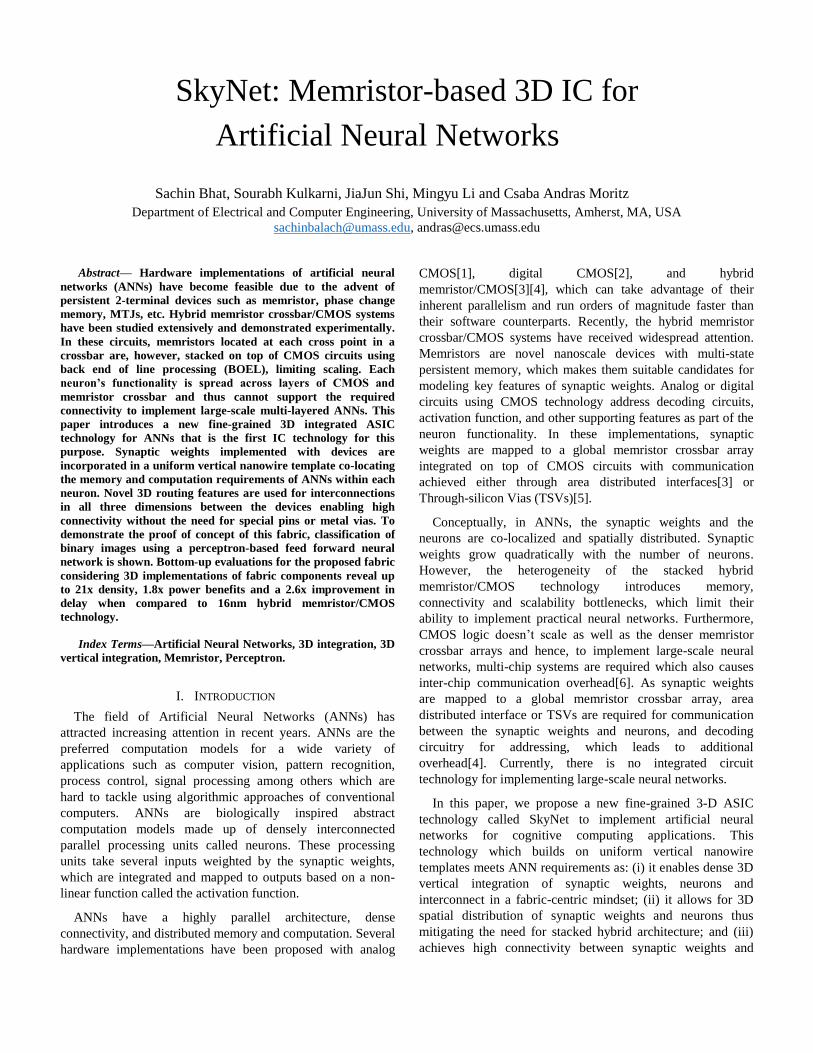
Fig. 1A shows an abstract model of a neuron with ‘n’
inputs. The inputs to the neuron can be any real values, with
each input having a weight associated with it. Strengths or
weights associated with the neurons are called synaptic
weights. The inputs are multiplied with their corresponding
synaptic weights and integrated at the neuron. The integrated
weighted inputs are fed to the activation function, which maps
it to a real value. Synaptic weights are used to store the
knowledge acquired by the network and can be changed to
attain the desired objective.
In layered neural networks, the neurons are organized in
multiple layers where input from previous layers feeds to the
next layer. This type of network is called Feedforward neural
network (Fig. 1B) and is used as an example in this paper.
Other configurations can also be supported. Different types of
ANNs differ mainly due to their activation function and
interconnection of nodes.
III. CORE FABRIC COMPONENTS
In hybrid memristor/CMOS systems connectivity between
the memristor crossbar arrays and underlying CMOS circuits
are engineered as an after-thought and is a compromise. As
ANNs scale in size, number of synapses and connections grow
quadratically which quickly becomes impractical to wire.
SkyNet follows a fabric-centric mindset where the active and
passive devices, circuit framework, and connectivity are
carefully engineered together towards a 3-D organization. Its
manufacturability requirement follows the same mindset as
other 3D IC fabrics (SkyBridge[7] and Skybridge-3D-
CMOS[8][9][10]). The fabric uses a regular array of uniform
pre-doped vertical nanowires as a template which is then
functionalized with vertical junctionless transistors,
memristors, 3D routing structures such as bridges, co-axial
routing structures, SkyBridge-Interlayer-Connection (SB-ILC),
etc., through material deposition techniques.
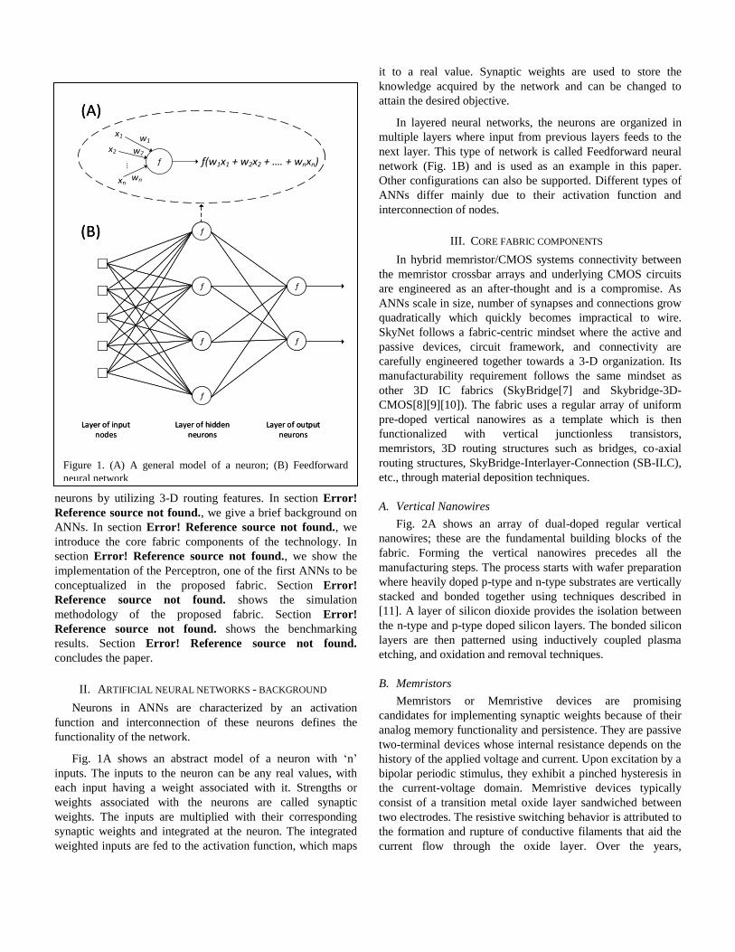
A. Vertical Nanowires
Fig. 2A shows an array of dual-doped regular vertical
nanowires; these are the fundamental building blocks of the
fabric. Forming the vertical nanowires precedes all the
manufacturing steps. The process starts with wafer preparation
where heavily doped p-type and n-type substrates are vertically
stacked and bonded together using techniques described in
[11]. A layer of silicon dioxide provides the isolation between
the n-type and p-type doped silicon layers. The bonded silicon
layers are then patterned using inductively coupled plasma
etching, and oxidation and removal techniques.
B. Memristors
Memristors or Memristive devices are promising
candidates for implementing synaptic weights because of their
analog memory functionality and persistence. They are passive
two-terminal devices whose internal resistance depends on the
history of the applied voltage and current. Upon excitation by a
bipolar periodic stimulus, they exhibit a pinched hysteresis in
the current-voltage domain. Memristive devices typically
consist of a transition metal oxide layer sandwiched between
two electrodes. The resistive switching behavior is attributed to
the formation and rupture of conductive filaments that aid the
current flow through the oxide layer. Over the years,
f f(w1x1 + w2x2 + wnxn)...
x1
x2
xnwn
w2
w1
Layer of input nodes
Layer of hidden neurons
Layer of output neurons
f
f
f
f
ff
(A)
(B)
f f(w1x1 + w2x2 + wnxn)...
x1
x2
xnwn
w2
w1
Layer of input nodes
Layer of hidden neurons
Layer of output neurons
f
f
f
f
ff
(A)
(B)
Figure 1. (A) A general model of a neuron; (B) Feedforward
neural network

memristors with several different oxide materials have been
proposed such as titanium dioxide[12] and hafnium
dioxide[13], to name few.
The proposed fabric uses titanium dioxide memristive devices
for synaptic weight implementation. Fig. 2B shows the
memristor device design. Memristors are distributed
throughout the fabric along with other fabric components with
fine granularity unlike stacked architectures in hybrid
memristor/CMOS systems. The titanium oxide based
memristors have an intrinsic rectifying property due to their
highly non-linear switching dynamics, and hence external
select devices such as transistors or diodes are not required for
their operation[14]. Since the aforementioned memristors can
be deposited with material deposition techniques, the
manufacturing requirements for them do not depart from that
of the other SkyNet components. They have similar feature
size as fabric components; as small as 10x10nm2 has been
experimentally demonstrated[13]. Since the silicon nanowires
are heavily doped, the inner electrode forms an ohmic contact.
This kind of structure is similar to the memristors with
asymmetric electrodes experimentally demonstrated in [15].
C. Vertical Gate-All-Around Junctionless Transistors
Vertical Gate-All-Around (V-GAA) junctionless p-type and
n-type transistors shown in Fig. 2C and Fig. 2D are the active
devices in the proposed fabric. These transistors have uniform
doping across source, channel and drain regions. The work
function difference between the gate electrode and the heavily
doped silicon nanowires modulates the behavior of these
transistors. Because of their structural simplicity, these
transistors can be stacked on the vertical nanowires to form 3-
D circuits. These types of transistors have been well researched
and also experimentally demonstrated by our group[16].
D. 3D Connectivity Features
The functionality of the ANNs depends on the
interconnection of the neurons in the network. In hybrid
memristor/CMOS systems, metal vias are used for connecting
CMOS neurons with the memristor crossbar arrays. This is
sufficient for very small-scale ANNs. However, for large-scale
ANNs, the wiring requirement explodes with the number of
synaptic weights. Hence, to efficiently implement ANNs, a
good interconnection framework is necessary. The proposed
fabric supports a sleuth of interconnect structures to
accommodate this connectivity without routing congestions. (i)
Bridges (Fig. 2G) are metal wires used for horizontal routing of
signals between nanowires; (ii) The heavily doped nanowires
can be used for vertical routing of signals; (iii) bridges for
horizontal routing; (iv) Co-axial routing structures (Fig. 2E)
can be used for vertical routing in addition to the nanowires;
and (v) SB-ILC (Fig. 2F) is for connecting n-type and p-type
nanowires when implementing circuits with the vertical GAA
transistors.
IV. PERCEPTRON IMPLEMENTATION
Perceptron is one of the first and simplest ANNs to be ever
conceptualized. The components of the perceptron closely
resemble that of the abstract neuron model shown in Fig 1A
with sigmoid function as the activation function. Fig. 3A shows
the hardware implementation of the perceptron with inputs
encoded as voltages (Vj). Memristors are used as synaptic
weights (wj) and a differential amplifier as the activation
function. Since negative weights cannot be implemented with
positive conductances, each weight w is implemented as a
differential pair of memristor conductances G = G+ - G-. The
input voltages are multiplied by conductances to generate
currents according to Ohm’s law. The currents corresponding
Figure 2. Core fabric components; (A) Dual-doped silicon nanowires; (B) Titanium dioxide memristor; (C) P-type V-GAA junctionless
transistor; (D) N-type V-GAA junctionless transistor; (E) Co-axial routing structure; (F) SkyBridge-Interlayer-connection (SB-ILC); (G)
Ohmic contact on n-type and p-type silicon with Tungsten bridges.
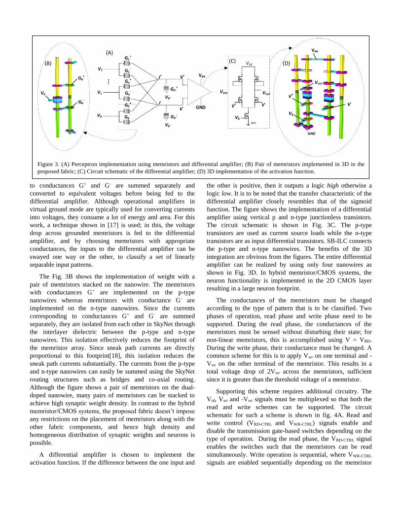
to conductances G+ and G- are summed separately and
converted to equivalent voltages before being fed to the
differential amplifier. Although operational amplifiers in
virtual ground mode are typically used for converting currents
into voltages, they consume a lot of energy and area. For this
work, a technique shown in [17] is used; in this, the voltage
drop across grounded memristors is fed to the differential
amplifier, and by choosing memristors with appropriate
conductances, the inputs to the differential amplifier can be
swayed one way or the other, to classify a set of linearly
separable input patterns.
The Fig. 3B shows the implementation of weight with a
pair of memristors stacked on the nanowire. The memristors
with conductances G+ are implemented on the p-type
nanowires whereas memristors with conductance G- are
implemented on the n-type nanowires. Since the currents
corresponding to conductances G+ and G- are summed
separately, they are isolated from each other in SkyNet through
the interlayer dielectric between the p-type and n-type
nanowires. This isolation effectively reduces the footprint of
the memristor array. Since sneak path currents are directly
proportional to this footprint[18], this isolation reduces the
sneak path currents substantially. The currents from the p-type
and n-type nanowires can easily be summed using the SkyNet
routing structures such as bridges and co-axial routing.
Although the figure shows a pair of memristors on the dual-
doped nanowire, many pairs of memristors can be stacked to
achieve high synaptic weight density. In contrast to the hybrid
memristor/CMOS systems, the proposed fabric doesn’t impose
any restrictions on the placement of memristors along with the
other fabric components, and hence high density and
homogeneous distribution of synaptic weights and neurons is
possible.
A differential amplifier is chosen to implement the
activation function. If the difference between the one input and
the other is positive, then it outputs a logic high otherwise a
logic low. It is to be noted that the transfer characteristic of the
differential amplifier closely resembles that of the sigmoid
function. The figure shows the implementation of a differential
amplifier using vertical p and n-type junctionless transistors.
The circuit schematic is shown in Fig. 3C. The p-type
transistors are used as current source loads while the n-type
transistors are as input differential transistors. SB-ILC connects
the p-type and n-type nanowires. The benefits of the 3D
integration are obvious from the figures. The entire differential
amplifier can be realized by using only four nanowires as
shown in Fig. 3D. In hybrid memristor/CMOS systems, the
neuron functionality is implemented in the 2D CMOS layer
resulting in a large neuron footprint.
The conductances of the memristors must be changed
according to the type of pattern that is to be classified. Two
phases of operation, read phase and write phase need to be
supported. During the read phase, the conductances of the
memristors must be sensed without disturbing their state; for
non-linear memristors, this is accomplished using V = VRD.
During the write phase, their conductance must be changed. A
common scheme for this is to apply Vwr on one terminal and -
Vwr on the other terminal of the memristor. This results in a
total voltage drop of 2Vwr across the memristors, sufficient
since it is greater than the threshold voltage of a memristor.
Supporting this scheme requires additional circuitry. The
Vrd, Vwr and -Vwr signals must be multiplexed so that both the
read and write schemes can be supported. The circuit
schematic for such a scheme is shown in fig. 4A. Read and
write control (VRD-CTRL and VWR-CTRL) signals enable and
disable the transmission gate-based switches depending on the
type of operation. During the read phase, the VRD-CTRL signal
enables the switches such that the memristors can be read
simultaneously. Write operation is sequential, where VWR-CTRL
signals are enabled sequentially depending on the memristor
Figure 3. (A) Perceptron implementation using memristors and differential amplifier; (B) Pair of memristors implemented in 3D in the
proposed fabric; (C) Circuit schematic of the differential amplifier; (D) 3D implementation of the activation function.

that needs to be written. Figure 2 shows the implementation of
the read/write circuitry in SkyNet. Co-axial routing structures
are used to supply the control signals to n and p-type vertical
junctionless transistors. SB-ILC is used to short the terminals
of the p-type and n-type transistors, which are connected to the
memristors through the bridges. This results in a very compact
implementation vs. state-of-the-art.
V. EVALUATION METHODOLOGY
A. Memristor Model
As mentioned earlier, titanium oxide memristors are
considered for this work. Verilog-A VTEAM[19] memristor
model compatible with HSPICE was chosen to model them. It
is a general model for voltage controlled memristors and is
used to fit the experimental results of titanium dioxide
memristors demonstrated in [20]. For these devices, due to
their high non-linear switching dynamics, the memristor
conductances can be read with VRD ≈ 0.8V without disturbing
the state of the memristors. For all memristors considered in
this work, Gmax = 5x10⁻⁴ S and Gmin = 5x10⁻⁵ S. The synaptic
weights can be set from - Gmax + Gmin to + Gmax -Gmin because of
the differential representation.
B. Device and Circuit-level Simulations
Device simulations for n-type and p-type vertical
junctionless transistors were characterized in our previous
work[21]. The simulation for other fabric components was also
shown. The TCAD device and process simulation data were
used to create behavioral models for HSPICE simulation.
The resistance and capacitance of the interconnect were
modeled using PTM[22]. 3D layouts that were manually built
using the 3D design rules in [7]. HSPICE simulations were
carried out to verify the functionality of the perceptron. Area
footprint was calculated based on the number of nanowires and
nanowire pitch.
VI. RESULTS
A single-layer perceptron is a feedforward neural network,
which is capable of classification of linearly separable patterns.
To validate correct functionality, we implement a single-layer
Figure 4. (A) Circuit schematic of the read/write circuit; (B) Read/write circuit implementation in Neuro-SkyBridge; (C) Perceptron in
Neuro-SkyBridge.
V1 V4 V7
V2 V5 V8
V3 V6 V9
Vb Vb
Bias Bias
f
f
f
W1,1
W3,b
...
0V
0.8V
(A) (B)
(C)
Pattern X Pattern T Pattern
Input nodes
Output neurons
Synaptic weights
V1 V4 V7
V2 V5 V8
V3 V6 V9
Vb Vb
Bias Bias
f
f
f
W1,1
W3,b
...
0V
0.8V
(A) (B)
(C)
Pattern X Pattern T Pattern
Input nodes
Output neurons
Synaptic weights
Figure 5. (A) 3x3 binary image pixels encoded as voltages; (B)
Single-layer perceptron used to classify the images; (C) Input
patterns considered for classification.
perceptron with 3 perceptrons, which can classify binary
images of 3x3 pixels. We completed detailed simulation
including a physical layer of such an implementation. The
functional scheme is shown in Fig. 5. It consists of 10 inputs,
32 synaptic weights, and three output perceptron to classify
three different input patterns ‘X’, ‘T’ and ‘+’. Inputs
corresponding to pixels are encoded using voltages V1 to V9.
The black pixels were encoded with 0V while the white pixels
with 0.8V. Since such patterns are linearly separable, there
exists a set of synaptic weights wi,j which enable successful
classification. The synaptic weights for such classification
were calculated using the perceptron learning rule[22].
Table I shows the single-layer perceptron benchmarking
results vs. the hybrid memristor/CMOS 16nm, which also was
completed. The proposed SkyNet design has 21x density
benefits, 2.6x improvement in latency and 1.8x power
efficiency over the hybrid stacked version. These density
benefits are substantial even at this small ANN. Larger designs
would benefit increasingly from the connectivity in this fabric
vs. state-of-the-art hybrid schemes due to the higher routing
demand in the stacked CMOS version that has no dedicated
resources for connecting the neurons between hidden layers in
an ANN.
TABLE I. Results of single-layer perceptron
Single-layer
perceptron Area
(um2)
Power
(uW)
Latency
(ps)
Proposed fabric 0.21 5.325 9.49
Hybrid memristor/ CMOS
4.59 13.845 17.085
VII. CONCLUSION AND FUTURE WORK
In this paper, we described the first architected 3D ASIC
technology for ANNs. Various fabric components are
introduced, and their use in the implementation of ANNs is
demonstrated. The fabric allows for co-localization of synaptic
weights and neurons, which is not possible with the hybrid
memristor/CMOS approach. For the example studied the
SkyNet achieves 21x density, 2.6x latency, and 1.8x power
efficiency benefits. We expect larger ANNs to accentuate
these benefits even further.
REFERENCES
[1] Mead, Carver. "Neuromorphic electronic systems." Proceedings of the
IEEE 78.10 (1990): 1629-1636.
[2] F. Akopyan et al., “TrueNorth: Design and Tool Flow of a 65 mW 1
Million Neuron Programmable Neurosynaptic Chip,” IEEE Trans. Comput. Des. Integr. Circuits Syst., vol. 34, no. 10, pp. 1537–1557,
2015.
[3] Strukov, Dmitri B., et al. "Hybrid CMOS/memristor circuits." Circuits
and Systems (ISCAS), Proceedings of 2010 IEEE International Symposium on. IEEE, 2010.
[4] Kim, Kuk-Hwan, et al. "A functional hybrid memristor crossbar-array/CMOS system for data storage and neuromorphic applications."
Nano Letters 12.1 (2011): 389-395.
[5] Sacchetto, Davide, et al. "Resistive programmable through-silicon vias for reconfigurable 3-D fabrics." IEEE Transactions on Nanotechnology
11.1 (2012): 8-11.
[6] Zamarreño-Ramos, Carlos, et al. "Multicasting mesh AER: a scalable
assembly approach for reconfigurable neuromorphic structured AER
systems. application to ConvNets." IEEE transactions on biomedical circuits and systems 7.1 (2013): 82-102.
[7] M. Rahman, S. Khasanvis, J. Shi, M. Li, C. A. Moritz. "Skybridge: 3D
Integrated Circuit Technology Alternative to CMOS." Available Online: http://arxiv.org/abs/1404.0607.
[8] Shi, Jiajun, et al. "NP-Dynamic Skybridge: A Fine-grained 3D IC Technology with NP-Dynamic Logic." IEEE Transactions on Emerging
Topics in Computing (2017).
[9] Li, Mingyu, et al. "Skybridge-3D-CMOS: A Vertically-Composed Fine-
Grained 3D CMOS Integrated Circuit Technology." VLSI (ISVLSI),
2016 IEEE Computer Society Annual Symposium on. IEEE, 2016.
[10] Li, Mingyu, et al. "Skybridge-3D-CMOS: A Vertically-Composed Fine-
Grained 3D CMOS Integrated Circuit Technology." IEEE Transactions
on Nanotechnology, In press, 2017.
[11] Batude, P., et al. "Advances in 3D CMOS sequential integration."
Electron Devices Meeting (IEDM), 2009 IEEE International. IEEE, 2009.
[12] Strukov, Dmitri B., et al. "The missing memristor found." nature
453.7191 (2008): 80-83.
[13] Govoreanu, B., et al. "10× 10nm 2 Hf/HfO x crossbar resistive RAM
with excellent performance, reliability and low-energy operation." Electron Devices Meeting (IEDM), 2011 IEEE International. IEEE,
2011.
[14] Yang, J. Joshua, et al. "Engineering nonlinearity into memristors for passive crossbar applications." Appl. Phys. Lett 100.11 (2012): 113501.
[15] Williamson, Adam, et al. "Synaptic behavior and STDP of asymmetric
nanoscale memristors in biohybrid systems." Nanoscale 5.16 (2013):
7297-7303.
[16] Rahman, Mostafizur, et al. "Experimental prototyping of beyond-CMOS nanowire computing fabrics." Nanoscale Architectures (NANOARCH),
2013 IEEE/ACM International Symposium on. IEEE, 2013.
[17] Yakopcic, Chris, et al. "SPICE analysis of dense memristor crossbars for
low power neuromorphic processor designs." Aerospace and Electronics
Conference (NAECON), 2015 National. IEEE, 2015.
[18] Zidan, Mohammed Affan, et al. "Memristor-based memory: The sneak
paths problem and solutions." Microelectronics Journal 44.2 (2013):
176-183.
[19] Kvatinsky, Shahar, et al. "VTEAM: A general model for voltage-
controlled memristors." IEEE Transactions on Circuits and Systems II: Express Briefs 62.8 (2015): 786-790.
[20] Alibart, Fabien, Elham Zamanidoost, and Dmitri B. Strukov. "Pattern classification by memristive crossbar circuits using ex-situ and in-situ
training." Nature Communications 4 (2013).
[21] Shi, Jiajun, et al. "Architecting NP-Dynamic Skybridge." Nanoscale Architectures (NANOARCH), 2015 IEEE/ACM International
Symposium on. IEEE, 2015.
[22] Arizona State University. PTM-MG device models for 16nm node,
<www.ptm.asu.edu>.
[23] Rosenblatt, Frank. "Principles of neurodynamics." (1962).