sis detector simulation with coupled antennas for detecting to...
TRANSCRIPT

IJCSNS International Journal of Computer Science and Network Security, VOL.17 No.11, November 2017
163
Manuscript received November 5, 2017 Manuscript revised November 20, 2017
SIS Detector Simulation with Coupled Antennas for Detecting to The Frequency Ghz40
Seyed Mohammad Larimian1, Alireza Erfanian2, Seyed Hossein Mohseni Armaki3
1.MA in Electronic, Malek Ashtar University, Tehran, Iran 2. Associate Professor, Electronic Faculty, Malek Ashtar University, Tehran, Iran, Corresponding Author
3.Associate Professor, Telecommunication Faculty, Malek Ashtar University, Tehran, Iran
Summary One type of superconducting detectors, which is based on the Josephson links is the SIS detectors, (superconductor-Insulator- superconductor), which has a high sensitivity. In this thesis, the SIS detector is designed with antenna (spiral and bow tie) to the frequency of GHz40. In the simulations, the designed antenna gains, depending on the type of antenna, is between dBi1.62 to dBi4.75 in the frequency of 30 to 40 GHz. Key words: SIS Detector - Antenna - Spiral - Bow Tie - Millimeter Wave.
1. Introduction
Millimeter waves, in the wavelength of 1 to 10 mm, equivalent to 30 to 300 GHz, are able to transmit through materials such as cloth, nylon, leather and so on, and also have a good transmission coefficient in fog and dust. Therefore, the use of systems that operate in this wavelength region, may help to see objects hidden under clothing, in suitcases or even see inside the walls, and also they can be used in foggy and misty weather and in landing aircraft, maritime patrol and rescue operations, aerial and land surveillance. Another application of using millimeter-wave systems is the detection of cosmic radiation in the wavelength region, leading to advances in astronomy affairs. Radar and communication systems, in this wavelength region have many developments.
Today, millimeter wave imaging systems are made in different structures, by using a variety of technologies, and researches are in progress in scientific and research centers to use new development and technologies. The most common technology that is used in commercial products, mainly in incoming inspections, critical and important facilities, such as airports are telecommunications receptor technology. These receptors, which serve as a radiometer, are primarily using a diode for a signal detector. In this area, making the diodes with greater sensitivity, at higher frequencies and their integration is today’s research, which are ongoing in the academic and research centers. In this study, the aim is simulating suitable superconducting detector for imaging in the millimeter wave region. For this purpose, the necessary steps should be taken.
2. The Use of Millimeter Waves
2.1. The Electromagnetic Spectrum
Electromagnetic waves are called in various names according to their frequency (wavelength): RF, millimeter wave, infrared (IR), terahertz, visible light, ultraviolet, X-rays and gamma rays. These names are arranged in order of increasing frequency [11].

IJCSNS International Journal of Computer Science and Network Security, VOL.17 No.11, November 2017
164
Fig. 1 The electromagnetic spectrum [11]
Table 1: Standard division of waves [12] Up to
frequency From the frequency Name of frequency spectrum In English
300 exahertz 30 exahertz Gamma-ray γ 30 exahertz 3 exahertz Hard X-ray HX
3 exahertz 30 petahertz Soft X-ray SX
33 petahertz 3 petahertz Far ultraviolet radiation EUV
3 petahertz 750 terahertz Near ultraviolet radiation NUV
750 terahertz 400 terahertz visible light Visible
400 terahertz 214 terahertz Near-infrared NIR
214 terahertz 100 terahertz Short wave infrared (terahertz) SIR
100 terahertz 37 terahertz Medium wave infrared (terahertz) MIR
37 terahertz 20 terahertz Long-wave infrared (terahertz) HIR
20 terahertz 300 gigahertz Far infrared (THz) FIR
300 gigahertz 30 gigahertz Ultra-high frequency (millimeter wave) EHF
30 gigahertz 3 gigahertz Very high frequency (microwave) SHF
3 gigahertz 300 megahertz Ultra-high frequency (microwave) UHF
300 megahertz 30 megahertz Very high frequency (microwave) VHF
30 megahertz 3 megahertz High frequency (microwave) HF
3 megahertz 300 kilohertz Medium frequency (microwave) MF
300 kilohertz 30 kilohertz Low frequency (microwave) LF
30 kilohertz 3 kilohertz Very low frequency (microwave) VLF
3 kilohertz 300 hertz In the audio frequency (microwave) VF
300 hertz 30 hertz Extremely Low Frequency ELF Physics of electromagnetic waves is a category of Physics of Waves, which has the following characteristics:
• Electromagnetic waves have the same nature and speed and only differ in terms of the frequency, or wavelength.
IJCSNS International Journal of Computer Science and Network Security, VOL.17 No.11, November 2017
165
• There is no gap in the spectrum of electromagnetic wave physics, which means we can produce any desired frequency. • There is no determined up or down limit to measure the frequency or wavelength.
2.2. Features and Capabilities of Millimeter Waves and Compared with Competing Technologies
2.2.1. The Reaction with the Atmosphere
Terahertz waves resonate by water vapor and absorb to it [12-13-4]. This phenomenon could be effective in applications related to astronomy, such as piles of dust and gas surrounding the galaxies, making the sensors on the earth move, terahertz telescope, etc. [8]
2.2.2. Reacting with Metals
These waves can react with metals easily. For example, for copper, deep into the skin in the normal radiation in frequency of one terahertz is 100 nm, and it cannot enter into the metal and have an intense reflection, and metal objects, which reflect largely, can be detected, while, they are covered with a cloth or paper or things like this that was mentioned above.
3. Types of Detectors Based on Superconducting
3.1. Transmission Edge Sensor (TES)
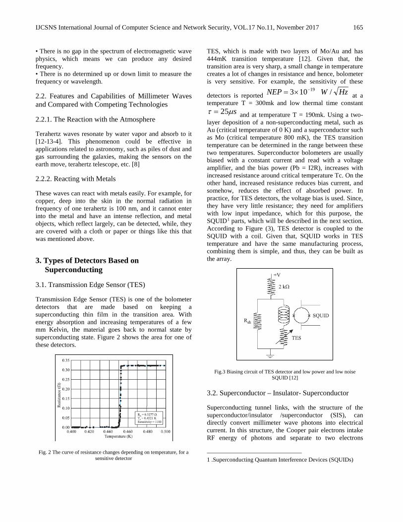
Transmission Edge Sensor (TES) is one of the bolometer detectors that are made based on keeping a superconducting thin film in the transition area. With energy absorption and increasing temperatures of a few mm Kelvin, the material goes back to normal state by superconducting state. Figure 2 shows the area for one of these detectors.
Fig. 2 The curve of resistance changes depending on temperature, for a
sensitive detector
TES, which is made with two layers of Mo/Au and has 444mK transition temperature [12]. Given that, the transition area is very sharp, a small change in temperature creates a lot of changes in resistance and hence, bolometer is very sensitive. For example, the sensitivity of these
detectors is reported at a temperature T = 300mk and low thermal time constant
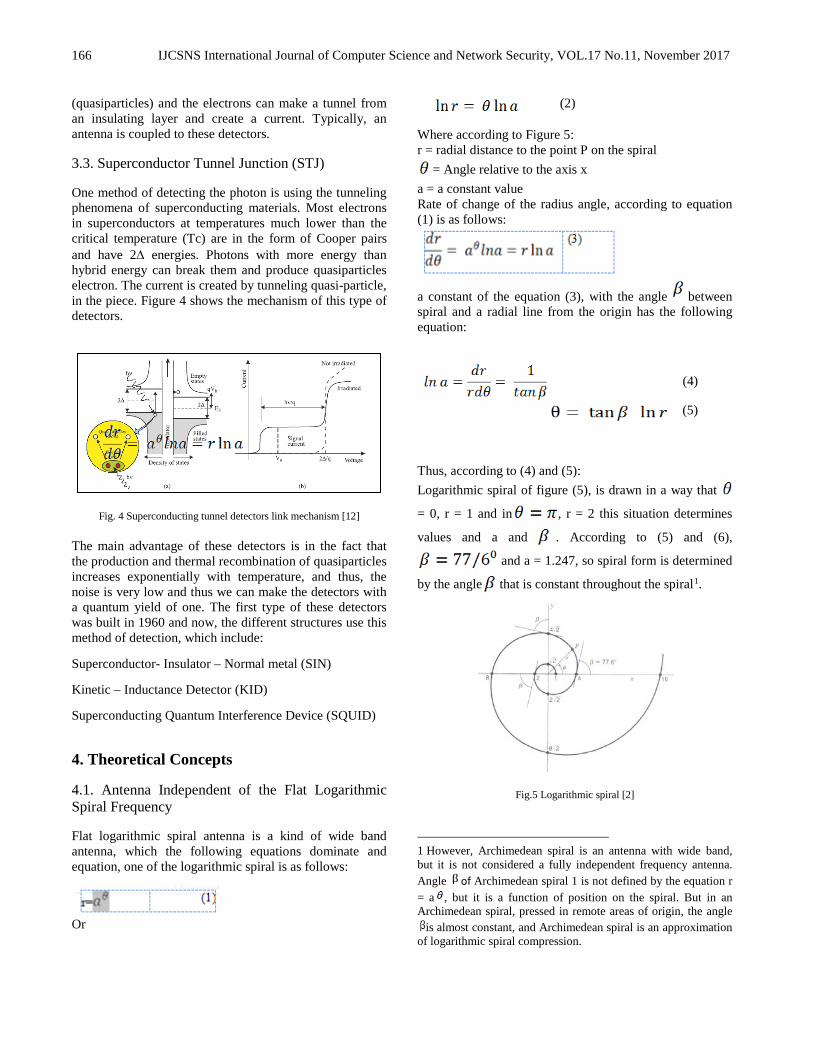
and at temperature T = 190mk. Using a two-layer deposition of a non-superconducting metal, such as Au (critical temperature of 0 K) and a superconductor such as Mo (critical temperature 800 mK), the TES transition temperature can be determined in the range between these two temperatures. Superconductor bolometers are usually biased with a constant current and read with a voltage amplifier, and the bias power (Pb = I2R), increases with increased resistance around critical temperature Tc. On the other hand, increased resistance reduces bias current, and somehow, reduces the effect of absorbed power. In practice, for TES detectors, the voltage bias is used. Since, they have very little resistance; they need for amplifiers with low input impedance, which for this purpose, the SQUID1 parts, which will be described in the next section. According to Figure (3), TES detector is coupled to the SQUID with a coil. Given that, SQUID works in TES temperature and have the same manufacturing process, combining them is simple, and thus, they can be built as the array.
Fig.3 Biasing circuit of TES detector and low power and low noise
SQUID [12]
3.2. Superconductor – Insulator- Superconductor
Superconducting tunnel links, with the structure of the superconductor/insulator /superconductor (SIS), can directly convert millimeter wave photons into electrical current. In this structure, the Cooper pair electrons intake RF energy of photons and separate to two electrons
1 .Superconducting Quantum Interference Devices (SQUIDs)
HzWNEP /103 19−×=
sµτ 25=
IJCSNS International Journal of Computer Science and Network Security, VOL.17 No.11, November 2017
166
(quasiparticles) and the electrons can make a tunnel from an insulating layer and create a current. Typically, an antenna is coupled to these detectors.
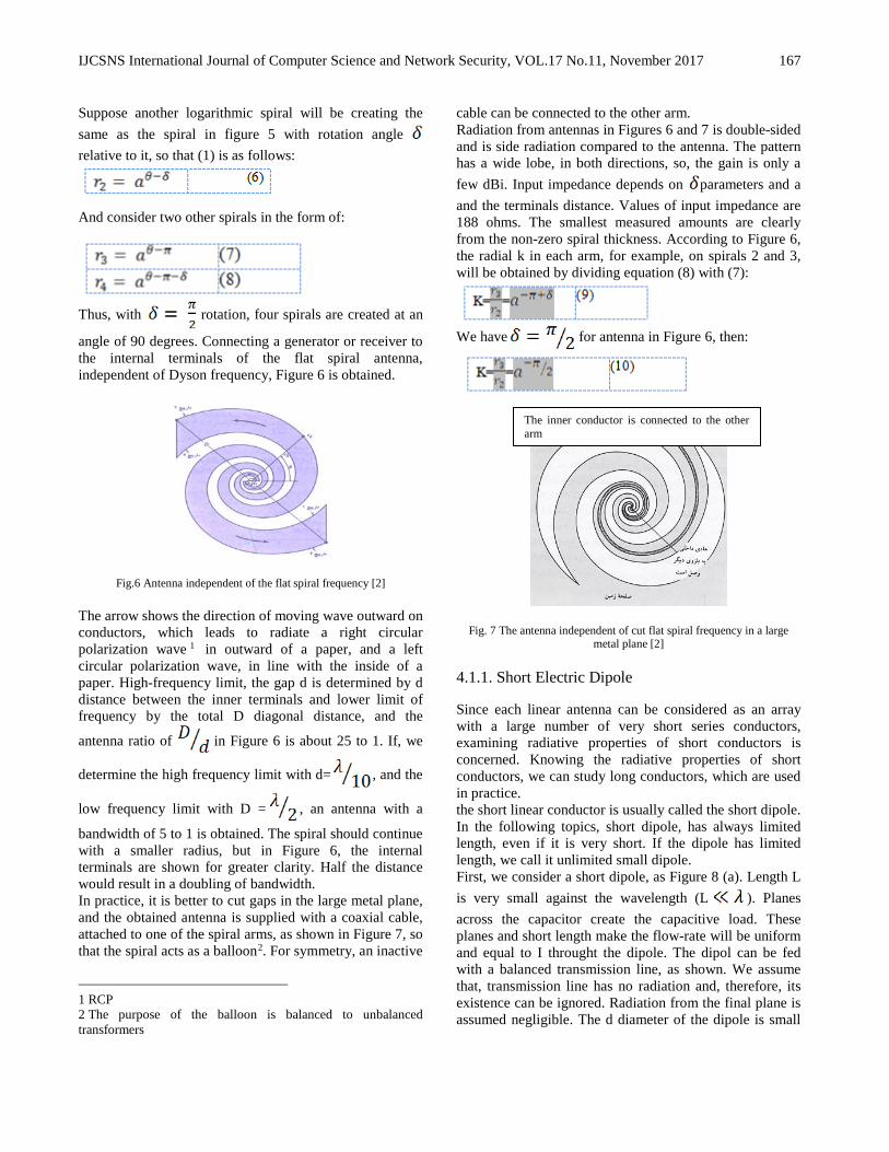
3.3. Superconductor Tunnel Junction (STJ)
One method of detecting the photon is using the tunneling phenomena of superconducting materials. Most electrons in superconductors at temperatures much lower than the critical temperature (Tc) are in the form of Cooper pairs and have 2∆ energies. Photons with more energy than hybrid energy can break them and produce quasiparticles electron. The current is created by tunneling quasi-particle, in the piece. Figure 4 shows the mechanism of this type of detectors.
Fig. 4 Superconducting tunnel detectors link mechanism [12]
The main advantage of these detectors is in the fact that the production and thermal recombination of quasiparticles increases exponentially with temperature, and thus, the noise is very low and thus we can make the detectors with a quantum yield of one. The first type of these detectors was built in 1960 and now, the different structures use this method of detection, which include:
Superconductor- Insulator – Normal metal (SIN)
Kinetic – Inductance Detector (KID)
Superconducting Quantum Interference Device (SQUID)
4. Theoretical Concepts
4.1. Antenna Independent of the Flat Logarithmic Spiral Frequency
Flat logarithmic spiral antenna is a kind of wide band antenna, which the following equations dominate and equation, one of the logarithmic spiral is as follows:
Or
(2)
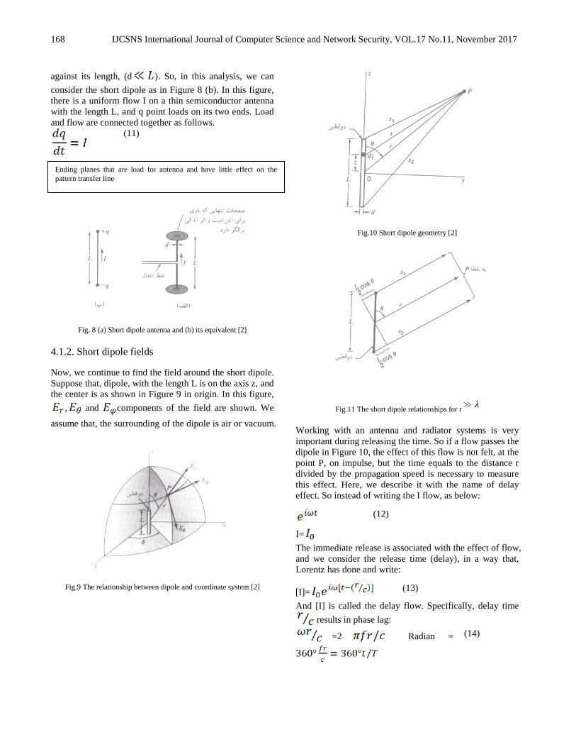
Where according to Figure 5: r = radial distance to the point P on the spiral
= Angle relative to the axis x a = a constant value Rate of change of the radius angle, according to equation (1) is as follows:
a constant of the equation (3), with the angle between spiral and a radial line from the origin has the following equation:
Thus, according to (4) and (5): Logarithmic spiral of figure (5), is drawn in a way that
= 0, r = 1 and in , r = 2 this situation determines
values and a and . According to (5) and (6), and a = 1.247, so spiral form is determined
by the angle that is constant throughout the spiral1.
Fig.5 Logarithmic spiral [2]
1 However, Archimedean spiral is an antenna with wide band, but it is not considered a fully independent frequency antenna. Angle of Archimedean spiral 1 is not defined by the equation r = a , but it is a function of position on the spiral. But in an Archimedean spiral, pressed in remote areas of origin, the angle
is almost constant, and Archimedean spiral is an approximation of logarithmic spiral compression.
)4(
(5)
IJCSNS International Journal of Computer Science and Network Security, VOL.17 No.11, November 2017
167
Suppose another logarithmic spiral will be creating the same as the spiral in figure 5 with rotation angle relative to it, so that (1) is as follows:
And consider two other spirals in the form of:
Thus, with rotation, four spirals are created at an
angle of 90 degrees. Connecting a generator or receiver to the internal terminals of the flat spiral antenna, independent of Dyson frequency, Figure 6 is obtained.
Fig.6 Antenna independent of the flat spiral frequency [2]
The arrow shows the direction of moving wave outward on conductors, which leads to radiate a right circular polarization wave 1 in outward of a paper, and a left circular polarization wave, in line with the inside of a paper. High-frequency limit, the gap d is determined by d distance between the inner terminals and lower limit of frequency by the total D diagonal distance, and the
antenna ratio of in Figure 6 is about 25 to 1. If, we
determine the high frequency limit with d= , and the
low frequency limit with D = , an antenna with a
bandwidth of 5 to 1 is obtained. The spiral should continue with a smaller radius, but in Figure 6, the internal terminals are shown for greater clarity. Half the distance would result in a doubling of bandwidth. In practice, it is better to cut gaps in the large metal plane, and the obtained antenna is supplied with a coaxial cable, attached to one of the spiral arms, as shown in Figure 7, so that the spiral acts as a balloon2. For symmetry, an inactive
1 RCP 2 The purpose of the balloon is balanced to unbalanced transformers
cable can be connected to the other arm. Radiation from antennas in Figures 6 and 7 is double-sided and is side radiation compared to the antenna. The pattern has a wide lobe, in both directions, so, the gain is only a few dBi. Input impedance depends on parameters and a and the terminals distance. Values of input impedance are 188 ohms. The smallest measured amounts are clearly from the non-zero spiral thickness. According to Figure 6, the radial k in each arm, for example, on spirals 2 and 3, will be obtained by dividing equation (8) with (7):
We have for antenna in Figure 6, then:
Fig. 7 The antenna independent of cut flat spiral frequency in a large
metal plane [2]
4.1.1. Short Electric Dipole
Since each linear antenna can be considered as an array with a large number of very short series conductors, examining radiative properties of short conductors is concerned. Knowing the radiative properties of short conductors, we can study long conductors, which are used in practice. the short linear conductor is usually called the short dipole. In the following topics, short dipole, has always limited length, even if it is very short. If the dipole has limited length, we call it unlimited small dipole. First, we consider a short dipole, as Figure 8 (a). Length L is very small against the wavelength (L ). Planes across the capacitor create the capacitive load. These planes and short length make the flow-rate will be uniform and equal to I throught the dipole. The dipol can be fed with a balanced transmission line, as shown. We assume that, transmission line has no radiation and, therefore, its existence can be ignored. Radiation from the final plane is assumed negligible. The d diameter of the dipole is small
The inner conductor is connected to the other arm
IJCSNS International Journal of Computer Science and Network Security, VOL.17 No.11, November 2017
168
against its length, (d ). So, in this analysis, we can consider the short dipole as in Figure 8 (b). In this figure, there is a uniform flow I on a thin semiconductor antenna with the length L, and q point loads on its two ends. Load and flow are connected together as follows.
)11(
Fig. 8 (a) Short dipole antenna and (b) its equivalent [2]
4.1.2. Short dipole fields
Now, we continue to find the field around the short dipole. Suppose that, dipole, with the length L is on the axis z, and the center is as shown in Figure 9 in origin. In this figure,
, and components of the field are shown. We
assume that, the surrounding of the dipole is air or vacuum.
Fig.9 The relationship between dipole and coordinate system [2]
Fig.10 Short dipole geometry [2]
Fig.11 The short dipole relationships for r
Working with an antenna and radiator systems is very important during releasing the time. So if a flow passes the dipole in Figure 10, the effect of this flow is not felt, at the point P, on impulse, but the time equals to the distance r divided by the propagation speed is necessary to measure this effect. Here, we describe it with the name of delay effect. So instead of writing the I flow, as below:
)12(
I= The immediate release is associated with the effect of flow, and we consider the release time (delay), in a way that, Lorentz has done and write:
)13( [I]= And [I] is called the delay flow. Specifically, delay time
results in phase lag: )14(
=2 Radian =
Ending planes that are load for antenna and have little effect on the pattern transfer line

IJCSNS International Journal of Computer Science and Network Security, VOL.17 No.11, November 2017
169
Where T = 1 / f the period of one cycle and f is frequency. Equation (14) is the expression of the fact that, a change, at time t, at a distance r from a flow element, is a result of changes that have happened in time t- (r /c) in the flow. The time lags r /c are the time required to publish changes to the distance r, c speed of light. We can express the electric and magnetic fields in terms of vector and scalar potentials. Since we are interested in near and far dipole fields, we should use delay potentials, which are statements include t-r /c. For dipole in Figure 9 or 10, delayed vector potential of electric current has only one component, that is . The value of this component is:
)15(
Where [I] is the delay flow and it is as follows: )16( =
In (16) and (17): Z = Point distance on the conductor
= Peak of uniform flow on the wire
= Permeability of free space If the distance to the dipole will be much larger than the length of the dipole (r and the wavelength will be
much larger than the length of the dipole (λ s = r and we can ignore the field phase shift caused by different sections of wire. In this case, Integral (16) can be considered constant and (16) can be written:
)17(
Delay scalar potential, V of a load distribution is as follows:
)18(
V=
Where [ ], delay load density is as follows:
)19( =
= Infinit small sized volume element
= Permittivity of free space Because in the study dipole, the zone containing endpoint loads are in Figure 8 (b), (18) will be as follows:
)20( V= { - }
And )21(
[q]=
Placing (21) in (20) gives:
)22( V= [ -
]
According to Figure 11, for r , we can consider the lines that are connected to the P point from the two ends of the dipole, parallel, so:
)23(
And
)24(
By placing (23) and (24) in (22), we can show that the field of an electric dipole are:
)25(
( )
)26(
)
= 1 is used in obtaining (25) and (26). Now, we focus our attention to the magnetic field, which can be obtained of Curl A, as follows:
)27(
= [ ] +
[ ] + [ ]
Since = 0, the first and fourth sentences (27) are zero,
and since and are independent of , second and

IJCSNS International Journal of Computer Science and Network Security, VOL.17 No.11, November 2017
170
third sentences (27), are also zero. So, two sentences are
remained and and as a result, H only has component. So:
)28(
)
)29(
Therefore, the dipole fields have only three , and
components. , and components are zero.
If r is very large, sentences 1/ and 1/ in (25), (26) and (28), can be ignored against the sentence 1/r. So the far field is negligible and in fact, only two field
components, and remains which include:
)30(
𝐸𝐸𝜃𝜃 = 𝑗𝑗𝑗𝑗𝑗𝑗0𝐿𝐿 sin𝜃𝜃𝑒𝑒𝑖𝑖𝑖𝑖[𝑡𝑡−(𝑟𝑟 𝑐𝑐⁄ )]
4𝜋𝜋𝜀𝜀0𝑐𝑐2𝑟𝑟=
j𝑗𝑗0𝛽𝛽𝐿𝐿4𝜋𝜋𝜀𝜀0𝑐𝑐𝑟𝑟
sin 𝜃𝜃 𝑒𝑒𝑖𝑖𝑗𝑗[𝑡𝑡−(𝑟𝑟 𝑐𝑐⁄ )]
)31(
𝐻𝐻𝜑𝜑 = 𝑗𝑗𝑗𝑗𝑗𝑗0𝐿𝐿 sin𝜃𝜃𝑒𝑒𝑖𝑖𝑖𝑖[𝑡𝑡−(𝑟𝑟 𝑐𝑐⁄ )]
4𝜋𝜋𝑐𝑐𝑟𝑟=
j𝑗𝑗0𝛽𝛽𝐿𝐿4𝜋𝜋𝑟𝑟
sin 𝜃𝜃 𝑒𝑒𝑖𝑖𝑗𝑗[𝑡𝑡−(𝑟𝑟 𝑐𝑐⁄ )]
The ratios 𝐸𝐸𝜃𝜃 3T to 𝐻𝐻𝜑𝜑 3T in (30) and (31) are as follows:
)32( 𝐸𝐸𝜃𝜃𝐻𝐻𝜑𝜑
= 1𝜀𝜀0𝑐𝑐
= �𝜇𝜇0𝜀𝜀0
=376.7𝛺𝛺
That is called the intrinsic impedance of free space and it is the pure resistance. Comparing (30) and (31) shows that, in far fields, 𝐸𝐸𝜃𝜃and 𝐻𝐻𝜑𝜑 has the same phase. Also, we see that the field pattern
of both is matched with𝑠𝑠𝑠𝑠𝑠𝑠 𝜃𝜃. The pattern is independent of𝜑𝜑, so, spatial pattern is obtained from the rotation of pattern in figure 12 around the dipole axis. According to near field statements in (25), (26) and (28), we see that an electric field has two components, for small r, 𝐸𝐸𝜃𝜃 and𝐸𝐸𝑟𝑟
that both have a phase difference with a magnetic field 90°, like fields inside the resonator, at average distance,
𝐸𝐸𝜃𝜃 and 𝐸𝐸𝑟𝑟 could almost have 90 ° phase difference, therefore, the total electric field vector rotates in a plane parallel to the release direction and the orthogonal field phenomenon occurs. For components𝐸𝐸𝜃𝜃 and𝐻𝐻𝜑𝜑, the near
field patterns are similar to the far field patterns and are matched with𝑠𝑠𝑠𝑠𝑠𝑠 𝜃𝜃 12. But the near field pattern 𝐸𝐸𝑟𝑟 is matched with𝑐𝑐𝑐𝑐𝑠𝑠 𝜃𝜃. Spatial pattern𝐸𝐸𝑟𝑟 as well, will be
obtained from the rotation of this pattern around a dipole axis.
Fig.12 (a) The near and far field patterns, short dipole components 𝐸𝐸𝜃𝜃و 𝐻𝐻𝜑𝜑 and (b) near-field pattern for 𝐸𝐸𝜃𝜃 component [2]
5. Simulation
5.1. Designing SIS Link
5.1.1. Obtaining SIS link
As mentioned before, if the link length is smaller than the Josephson penetration length, it is said to be short Josephson’s link. In this dissertation, manufacturing constraints caused the minimum dimensions of the SIS link will be 40 micrometers in 40 micro meter and by considering these considerations, we determine the value of critical current density.
(33) 𝜑𝜑0=2.07× 10⁻⁷𝐺𝐺𝑐𝑐𝑐𝑐2
𝜇𝜇0 = 1.256 × 10⁻⁶ 𝑁𝑁 𝐴𝐴2� d′ ≅ 160𝑠𝑠𝑐𝑐
𝜆𝜆𝑗𝑗 = �𝜑𝜑0
2𝜋𝜋𝜇𝜇0𝑗𝑗𝑐𝑐𝑑𝑑′ 𝑗𝑗𝑐𝑐 = 625𝐴𝐴 𝑐𝑐𝑐𝑐2�
According to the experiences of the manufacturing in superconducting lab, it is possible to make a link with certain critical flow density.
5.1.2. Determine the Specification of SIS Link
As shown below, the parameters of an SIS link, which are important in the design, include 𝐺𝐺𝑛𝑛 and 𝐶𝐶𝑗𝑗 and these parameters depend on physical characteristics and geometry dimensions of the link. The link capacitor (𝐶𝐶𝑗𝑗) can be obtained from the following equation.

IJCSNS International Journal of Computer Science and Network Security, VOL.17 No.11, November 2017
171
(34) 𝐶𝐶𝑗𝑗 = 𝜀𝜀
𝐴𝐴𝑑𝑑
Where, A is cross- section of the link and𝜀𝜀 = 𝜀𝜀0𝜀𝜀𝑟𝑟 is the coefficient of permittivity index and d is the thickness of the insulating layer. Also, 𝐺𝐺𝑛𝑛is obtained from the following formula
(35) 𝐺𝐺𝑛𝑛= 𝐴𝐴𝑔𝑔𝑛𝑛 Where 𝑔𝑔𝑛𝑛is the conductivity of the insulation, in the area and depends on the material of superconducting and the type and the thickness of insulation and the process of making link and there is no certain formulation, for it. In order to obtain it, for an identified insulating material and superconductivity, it can be measured in a single manufacturing process, for different thickness of the insulating layer, and use it as a reference for the design. The ability to detect SIS link is due to the nonlinear properties of the flow resulting from normal electron tunneling in this link. 𝐶𝐶𝑗𝑗Capacitors spend part of link flow on charging and discharging of the link and do not attend in the tunneling process, thus for having an ideal SIS link, the value of the capacitor should be zero, therefore, for having detectors, with more bandwidth, links with fewer capacitors should be used, but due to constraints on the construction of the lower dimensions that we can build, the dimensions with the width and length of 40𝜇𝜇𝑐𝑐, can be made and we design with these dimensions in this research, as a result, we have:
(36) 𝜀𝜀0 = 8.85 × 10⁻¹²
𝐹𝐹𝑐𝑐
𝜀𝜀𝑟𝑟 ≅ 40𝐹𝐹𝑐𝑐
𝜇𝜇𝑐𝑐 × 40𝜇𝜇𝑐𝑐 = 1600𝜇𝜇𝑐𝑐2 A=40 d =2nm
𝐶𝐶𝑗𝑗 = 𝜀𝜀0𝜀𝜀𝑟𝑟𝐴𝐴𝑑𝑑≅ 282𝑃𝑃𝐹𝐹
The amount of𝐺𝐺𝑛𝑛 is usually in the SIS detectors between 0.01𝛺𝛺−1 and 0.1𝛺𝛺−1 that in this study, according to the values obtained in the laboratory of superconductivity, approximately 0.1𝛺𝛺−1 is obtained.
5.1.3. Selecting Bias Voltage for SIS Link
In this link, the response of the flow in the ideal state in
the distance𝑉𝑉𝑔𝑔 −ℏ𝑗𝑗𝑠𝑠𝑒𝑒
< 𝑉𝑉𝑜𝑜 < 𝑉𝑉𝑔𝑔, is equal to ℏ𝑗𝑗𝑠𝑠𝑒𝑒
and
in the distance 𝑉𝑉𝑔𝑔 < 𝑉𝑉𝑜𝑜 < 𝑉𝑉𝑔𝑔 + ℏ𝑗𝑗𝑠𝑠𝑒𝑒
is equal -ℏ𝑗𝑗𝑠𝑠𝑒𝑒
, which is equal to its quantum limit, and outside of this distance, the value of this quantity is zero. For a real link, the response of the flow is in the form of the curve, thus,
for optimal performance, the bias voltage link must be
selected approximately equal to𝑉𝑉𝑔𝑔 ± ℏ𝑗𝑗𝑠𝑠2𝑒𝑒
, and otherwise, responding SIS link flow, which has a direct effect on the detection gain, will be low for the desired frequency. Since, the impact noise is as the most important component of the noise in the SIS link, from the dc flow of the link and the dc flow of the link increases suddenly with an increase in dc link voltage of the amount of𝑉𝑉𝑔𝑔, so, two
of the above selects the𝑉𝑉𝑔𝑔 −ℏ𝑗𝑗𝑠𝑠2𝑒𝑒
amount. [8] ℏ ≅ 1.05 × 10⁻³⁴𝐽𝐽. 𝑠𝑠 f =35GHz e ≅ 1.6 × 10⁻¹⁹𝐶𝐶 𝑉𝑉𝑔𝑔 = 2.9𝑐𝑐𝑉𝑉
V= 𝑉𝑉𝑔𝑔 −ℏ𝑗𝑗𝑠𝑠2𝑒𝑒
≅ 2.8𝑐𝑐𝑉𝑉
(37)
5.2. The Design of Antennas
Now, due to the above conditions, we design the antennas, that we design and simulate two antennas (Spiral Antenna and bow tie Antenna).
5.2.1. Antenna Independent of the Logarithmic Flat Spiral Frequency
Table 2. Overall specifications of spiral antenna [4] Quantity Typical Minimum Maximum
Polarisation Circular - - Radiation pattern Bi-directional
broadside lobes - -
Gain 5 dBi 4 dBi 6 dBi Performance bandwidth
5:1 1.5:1 (40 %)
> 10:1
Complexity Medium - -
The lowest radius of the spiral part is determined by the highest frequency, and the maximum radius is determined by the low frequency of the antenna. For frequencies of 30 to 40 GHz, the radius of the antenna is calculated as follows.
(38) 𝑟𝑟1 ≈
𝐶𝐶2𝜋𝜋�𝜀𝜀𝑟𝑟𝑒𝑒𝑟𝑟𝑟𝑟𝑓𝑓𝑚𝑚𝑚𝑚𝑚𝑚
=3 × 10⁸
2𝜋𝜋√2.2 × 40 × 109= 0.8𝑐𝑐𝑐𝑐
(39) 𝑟𝑟2 ≈
𝐶𝐶2𝜋𝜋�𝜀𝜀𝑟𝑟𝑒𝑒𝑟𝑟𝑟𝑟𝑓𝑓𝑚𝑚𝑖𝑖𝑛𝑛
=3 × 10⁸
2𝜋𝜋√2.2 × 30 × 109= 1.07𝑐𝑐𝑐𝑐
The number of rounds can be obtained from the following formula
(40) N=𝑟𝑟2−𝑟𝑟14𝑤𝑤
= 1.07−0.84×0.25
= 0.27 In practice, 𝑟𝑟1radius should be lower than the amount

IJCSNS International Journal of Computer Science and Network Security, VOL.17 No.11, November 2017
172
above, and the𝑟𝑟2 radius should be more than the obtained amount that as a result, it will increase the number of rounds. By selecting 𝑟𝑟1 = .011𝑐𝑐𝑐𝑐 and 𝑟𝑟2 =7.765𝑐𝑐𝑐𝑐 and the number of 2.16 rounds, the following results are obtained.
Fig.13 View of Designed Spiral
Fig.14 Designed spiral pattern in the frequencies 30, 35 and 40 GHz
5.2.2. Designing the bow tie antenna
Bow antenna is the modified form of the dipole antenna [6] that is often appropriate for wide band frequency interval without increasing complexity, and given the simplicity, it has a logical performance [10]. This antenna is generally used in the UHF range to the millimeter wave range, and also, the antenna can be used in arrays. The bow tie antenna is not sensitive to small changes in parameters and therefore, it improves the manufacturing errors. This antenna has a good gain between 1 dBi to 4.5 dBi with the broad bandwidth. A bow tie antenna is an omnidirectional antenna on H plane. Its broadband performance, in principle, is limited by its pattern performance, so that the pattern is ideal in frequencies close to𝑓𝑓𝑚𝑚𝑖𝑖𝑛𝑛 and 2𝑓𝑓𝑚𝑚𝑖𝑖𝑛𝑛 and in the frequencies of 3𝑓𝑓𝑚𝑚𝑖𝑖𝑛𝑛 and more, the pattern of the antenna will be non-ideal, but a 3: 1 antenna can be designed [10-7] and due to the limited operating frequency of this research, we use the antenna in this dissertation. For designing an antenna with suitable gain, we design the antenna in transmission mode and calculate its gain.
Table 3. The general specifications of bow tie antenna [1] Maximum Minimum Typical Quantity
- - Linear Polarisation - - Omnidirectional
in a plane Radiation
pattern 4.5 dBi 1 dBi 4 dBi Gain
3:1 1.5:1 2:1 Performance bandwidth
- - Simple Complexity According to what was mentioned, as shown below, we design an antenna with flare angle of 60 degrees, 3.17 mm arm's length, feed gap distance of 83 micrometers, and feed width of 100 micrometers that the results of the simulations are as below.
Fig.15 View of the bow designed in the first stage
Table 4. The specification of the designed bow tie in the first stage Name Description Value
La Arm length 3.177 mm Wf Feed width 100 μm Sf Feed gap 83 μm θ f Flare angle 60 °
The pattern of the antenna in the frequency of 30 GHz, 35

IJCSNS International Journal of Computer Science and Network Security, VOL.17 No.11, November 2017
173
GHz and 40 Ghz is in the form below:
Fig. 16 Bow tie pattern designed in the first stage at frequencies of 30, 35 and 40 GHz
The simulation results are matched with what was mentioned in the theory, and this antenna, with this specification, has a good gain.
SIS link dimensions are 40 micrometers in 40 micrometers, and according to the gap distance in the obtained design of these dimensions is smaller than the gap distance. Therefore, in the stimulations, we consider the limitation of the size and consider the gap distance 40 micrometers, and according to it, we perform the simulations that the antenna with the following characteristics is obtained.
Fig.17 View of the designed bow ties in the second stage
Table 5. The specification of the designed bow tie in the second stage Name Description Value
La Arm length 3.177 mm Wf Feed width 40 μm Sf Feed gap 40 μm θ f Flare angle 85 °
The pattern of the antenna in the frequency 30 GHz, 35 GHz and 40 GHz are in the form below.
IJCSNS International Journal of Computer Science and Network Security, VOL.17 No.11, November 2017
174
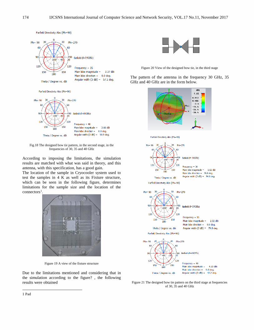
Fig.18 The designed bow tie pattern, in the second stage, in the frequencies of 30, 35 and 40 GHz
According to imposing the limitations, the simulation results are matched with what was said in theory, and this antenna, with this specification, has a good gain. The location of the sample in Cryocooler system used to test the samples in 4 K as well as its Fixture structure, which can be seen in the following figure, determines limitations for the sample size and the location of the connectors1.
Figure 19 A view of the fixture structure
Due to the limitations mentioned and considering that in the simulation according to the figure? , the following results were obtained
1 Pad
Figure 20 View of the designed bow tie, in the third stage
The pattern of the antenna in the frequency 30 GHz, 35 GHz and 40 GHz are in the form below.
Figure 21 The designed bow tie pattern on the third stage at frequencies of 30, 35 and 40 GHz

IJCSNS International Journal of Computer Science and Network Security, VOL.17 No.11, November 2017
175
As it is shown in the figure, the viewing angle has decreased in the frequency of 40 GHz, but given the proper gain, this problem can be ignored.
6. Conclusion
Logarithmic spiral antenna with dBi3-dBi4.75 gain was designed and simulated at frequencies (40-30) GHz and the gain can be matched with the values that were discussed in theory, and, the antenna can be used.
Bow tie antenna with the gain from dBi1.62 to dBi4.13 was designed and simulated at frequencies (40-30) GHz and this gain can be matched with the values that were discussed in theory, and the antenna can be used.
6.1. The Future Suggestions
- Given the wide frequency band of spiral antenna and the ability to detect SIS link, in GHz frequencies, to the extent 1000 GHz designing the SIS detector should be done in this frequency range.
- Analysis of analytical methods of transmission lines, antennas, filters and other microwave devices that superconductors have been used in them rather than metal. This could, eventually, lead to an appropriate application for analysis and the detailed design of the superconducting microwave devices.
- Optimal design of a complete milimeter and submillimeter wave detector system of superconducting, such as different combinations in the configuration of a detector, integrated superconducting (ie series and parallel combinations of SIS links).
References [1] Ilari Khusheh Mehri, making the Salitani diode, Master
Thesis, autumn 2010. [2] Kraus and Marfka, antenna, translator Mahmoud Diani,
third edition, 2005. [3] David J. Griffiths. Introduction to Electrodynamics (2nd
Edition). Prentice Hall ،1989. [4] Fixsen, D.J., Bennett, C.L and Mather, J.C., COBE FIRAS
OBSERVATIONS OF GALACTIC LINES, Astrophysical Journal, 526, 207,1999.
[5] J.D., Dyson, R. Bawer, P.E. Mayes, J.I. Wolfe,“A Note on the Difference Between Equiangular and Archimedes Spiral Antennas (Correspondence) “IRE Transactions on microwave Theory and Techniques, vol. 9, pp. 203—205, March 1961.
[6] K. L. Shlager, G. S. Smith, J.G. Maloney, “Optimization of bow-tie antennas for pulse radiation”, IEEE Transactions on Antennas and Propagation,vol. 42, pp. 975—982, July 1994.
[7] M. Bailey,” Broad-band half-wave dipole”, IEEE Transactions on Antennas and Propagation, vol 32, pp 410 – 412, Apr 1984.
[8] Pieternel, F., Levelt, E., Hilsenrath, G.W,. Leppelmeier, C.H.J., Van den Oord, P.K., Bhartia, J., Tamminen, J.F., de Hann, J.P and Veefkind, J.P., Science objectives of the of the ozone monitoring instrument.IEEE Trans. On Geoscience And Remote Sensing.44, 1199, 2006.
[9] Prof. Dr. Rudolf Gross andDr. Achim Marx ’’Applied Superconductivity:Josephson Effect and Superconducting Electronics’’ Manuscript to the Lectures during WS 2003/2004, WS 2005/2006, WS 2006/2007,WS 2007/2008, WS 2008/2009, and WS 2009/2010
[10] R. C. Compton, R. C. McPhedran, Z. Popovic, G. M. Rebeiz, P. P. Tong and D. B. Rutledge, "Bow-tie antennas on a dielectric half-space: theory and experiment", IEEE Transactions on Antennas and Propagation, vol. 35, pp. 622 – 631, June 1987.
[11] Ronald G. Driggers,Introduction to Infrared and Electro-Optical Systems, Artech House,1998
[12] Withington, S.,Terahertz astronomical telescopes and instrumentation, Trans. R. Soc. Lond. A,362,395-402. 2004.
[13] Woolard, D., Loerop,W and Shur,M.S and Editors, Terahertz Sensing Technology, Volumw II.Emergining Scientific Application and Novel Device Concepts, World Scientific, ISBN 981-238-611-4. 2003.