single-photon imaging in complementary metal oxide semiconductor processes by e. charbon...
TRANSCRIPT
Single-photon imaging in complementary metal oxide semiconductor processes
by E. Charbon
Philosophical Transactions AVolume 372(2012):20130100
March 28, 2014
©2014 by The Royal Society
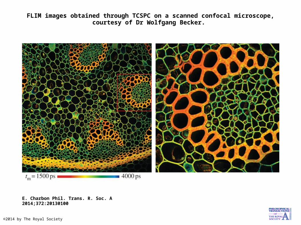
FLIM images obtained through TCSPC on a scanned confocal microscope, courtesy of Dr Wolfgang Becker.
E. Charbon Phil. Trans. R. Soc. A 2014;372:20130100
©2014 by The Royal Society

Histograms of the response of OGB-1 molecules to repeated excitation in the presence of Ca2+ ions at various concentrations [3].
E. Charbon Phil. Trans. R. Soc. A 2014;372:20130100
©2014 by The Royal Society
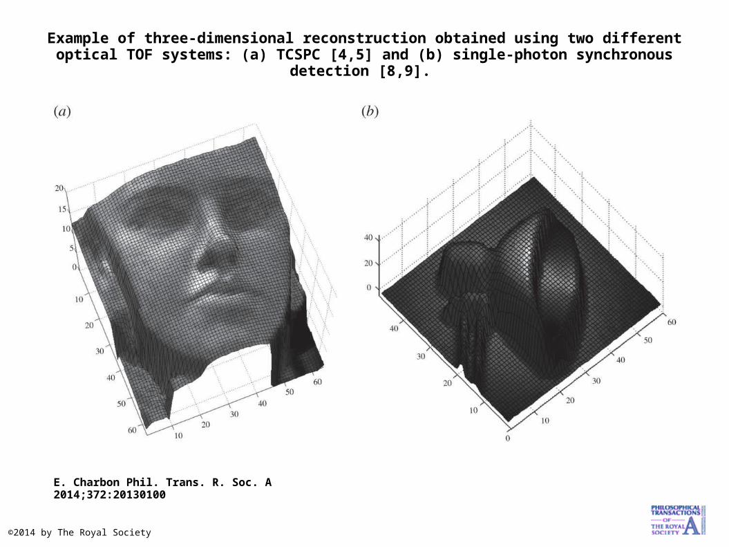
Example of three-dimensional reconstruction obtained using two different optical TOF systems: (a) TCSPC [4,5] and (b) single-photon synchronous detection [8,9].
E. Charbon Phil. Trans. R. Soc. A 2014;372:20130100
©2014 by The Royal Society
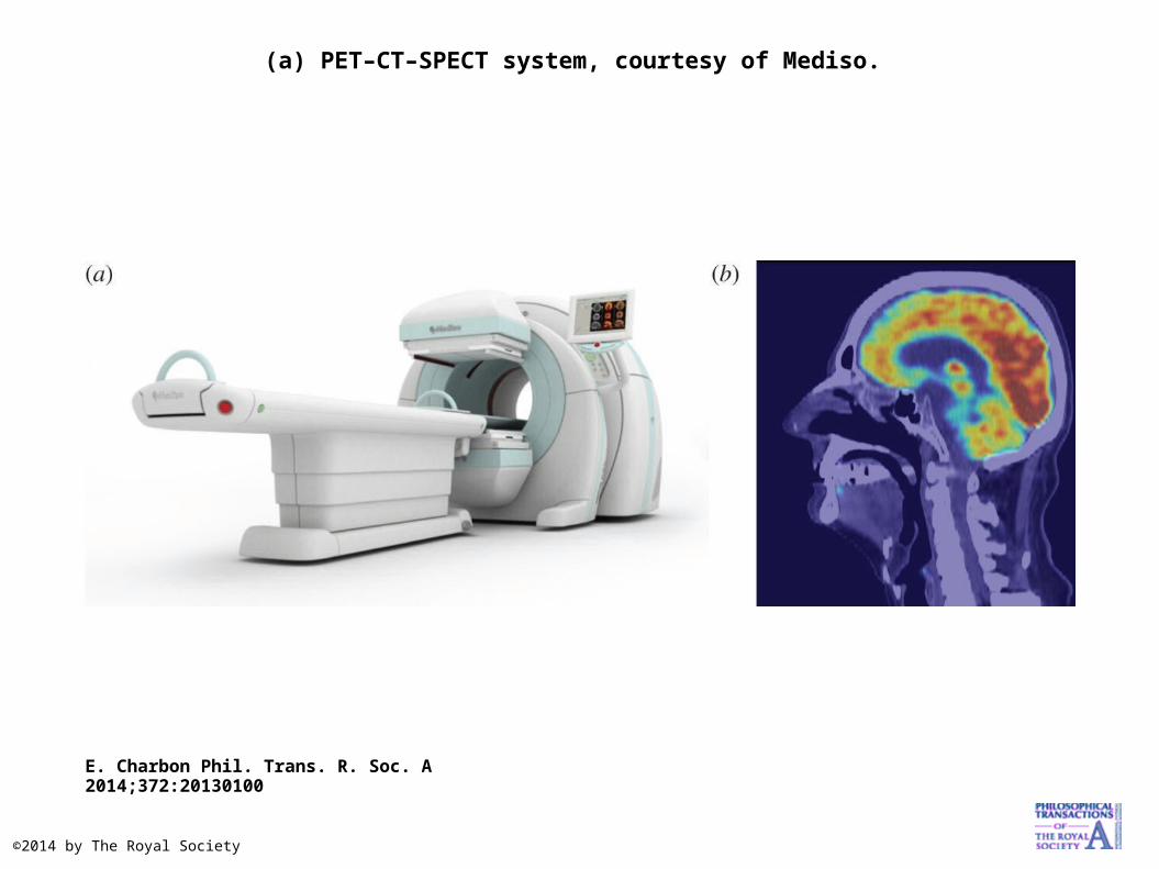
(a) PET–CT–SPECT system, courtesy of Mediso.
E. Charbon Phil. Trans. R. Soc. A 2014;372:20130100
©2014 by The Royal Society
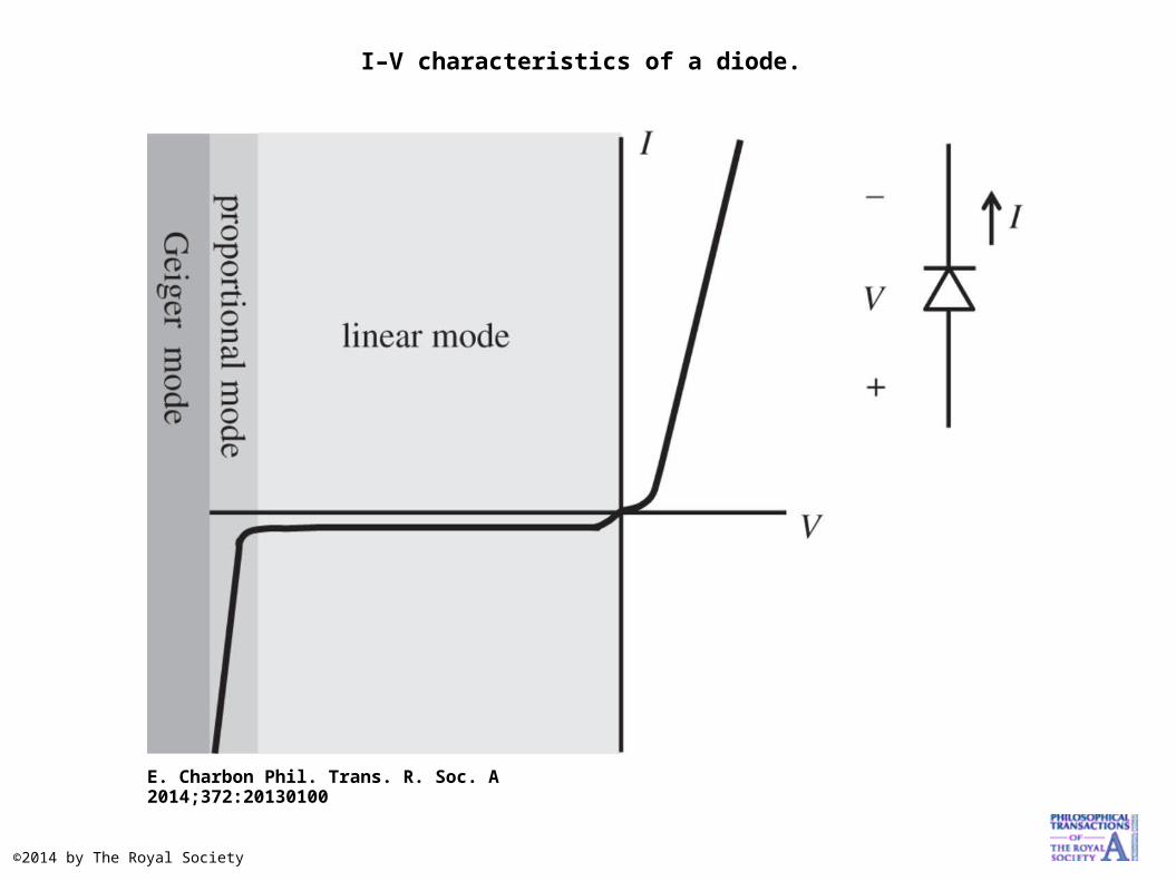
I–V characteristics of a diode.
E. Charbon Phil. Trans. R. Soc. A 2014;372:20130100
©2014 by The Royal Society

(a) SPAD with passive quenching and recharge circuit and (b) simple quantitative model.
E. Charbon Phil. Trans. R. Soc. A 2014;372:20130100
©2014 by The Royal Society
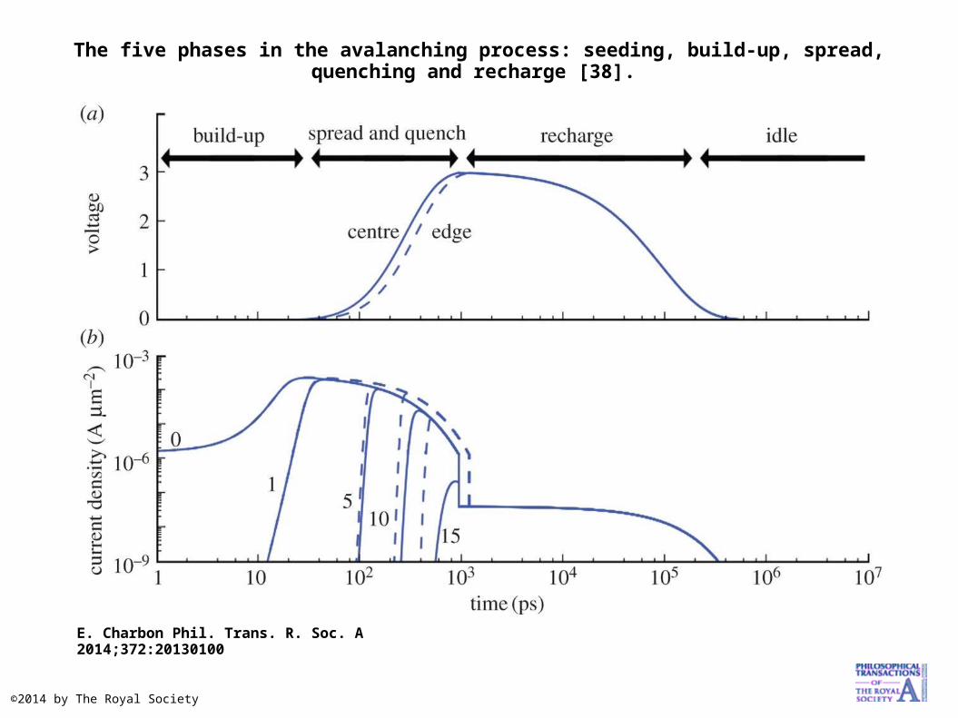
The five phases in the avalanching process: seeding, build-up, spread, quenching and recharge [38].
E. Charbon Phil. Trans. R. Soc. A 2014;372:20130100
©2014 by The Royal Society
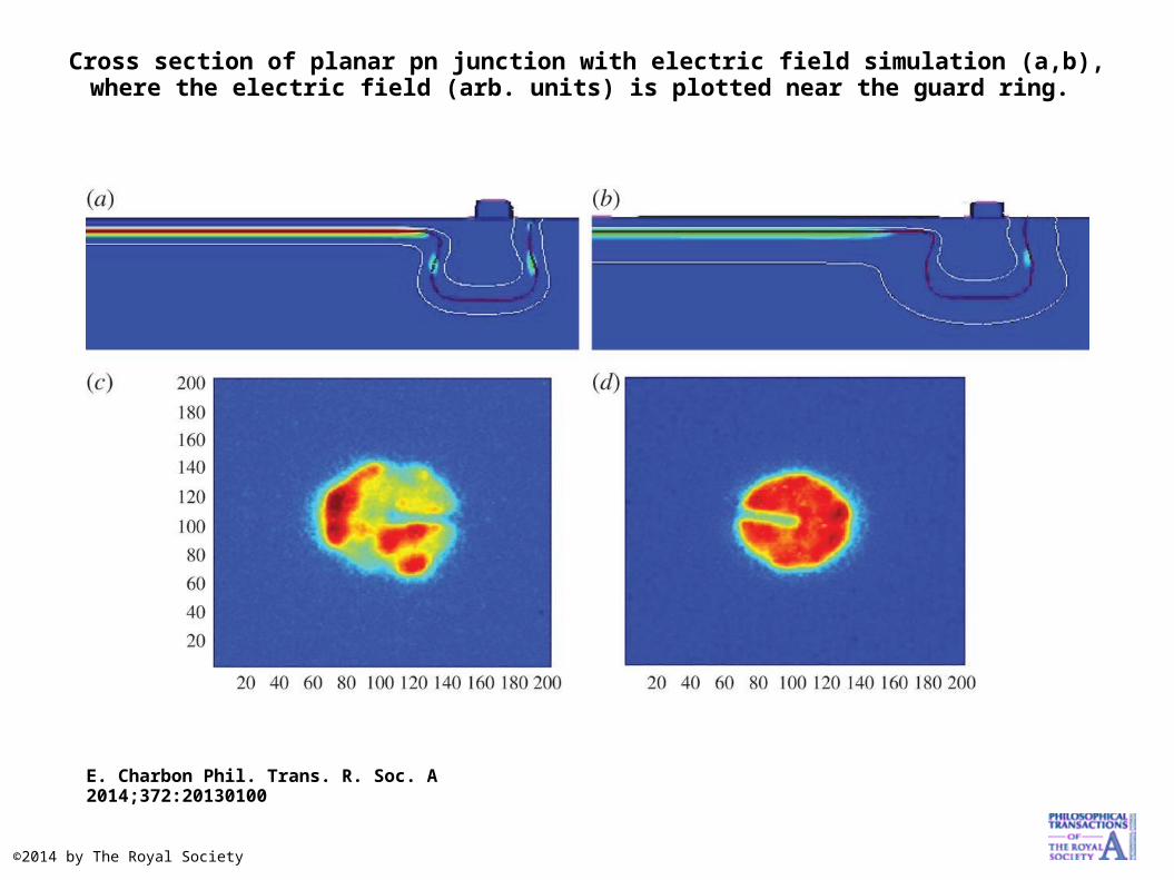
Cross section of planar pn junction with electric field simulation (a,b), where the electric field (arb. units) is plotted near the guard ring.
E. Charbon Phil. Trans. R. Soc. A 2014;372:20130100
©2014 by The Royal Society

Premature edge breakdown prevention mechanisms in planar and semi-planar processes.
E. Charbon Phil. Trans. R. Soc. A 2014;372:20130100
©2014 by The Royal Society
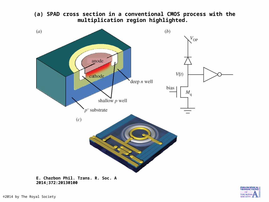
(a) SPAD cross section in a conventional CMOS process with the multiplication region highlighted.
E. Charbon Phil. Trans. R. Soc. A 2014;372:20130100
©2014 by The Royal Society

Active recharge mechanisms: (a) single-slope and (b) double-slope.
E. Charbon Phil. Trans. R. Soc. A 2014;372:20130100
©2014 by The Royal Society

Photo response in actively recharged SPADs [4], where saturation frequency is fsat=1/tdead.
E. Charbon Phil. Trans. R. Soc. A 2014;372:20130100
©2014 by The Royal Society
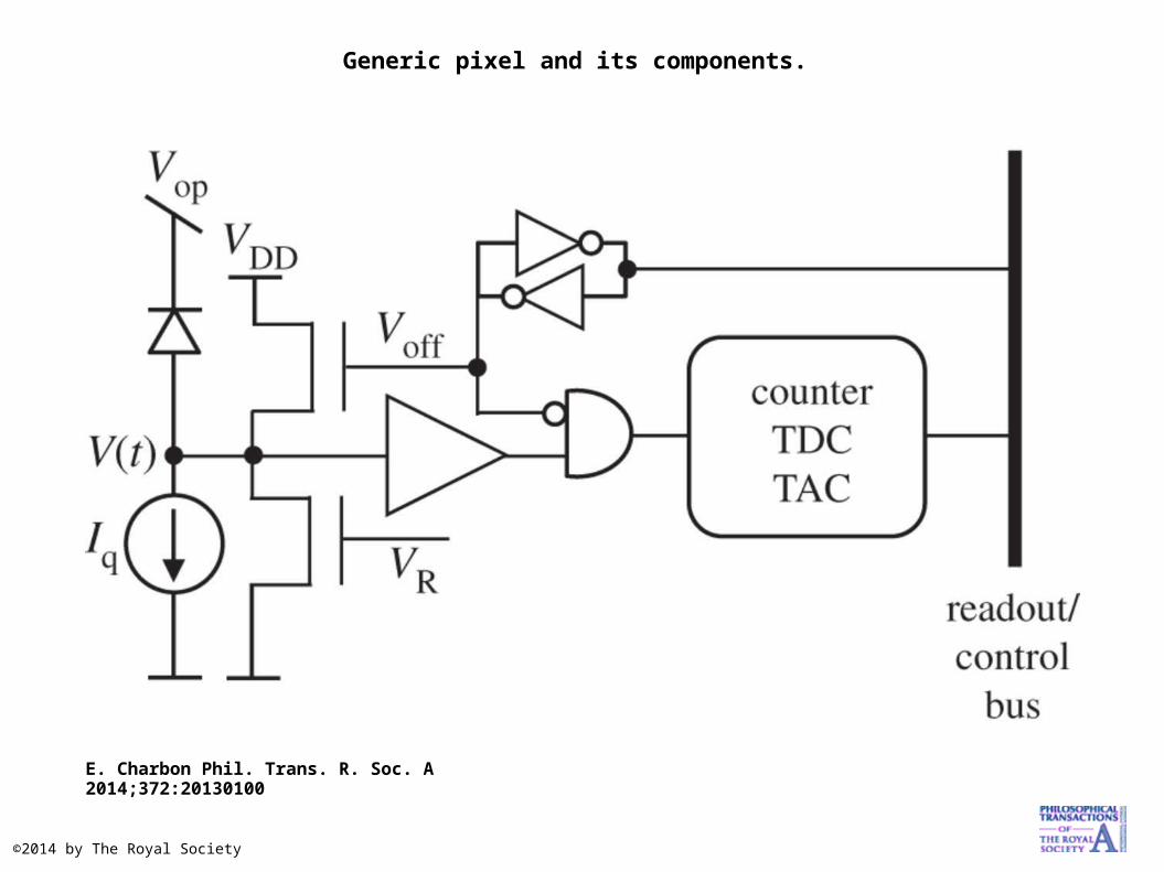
Generic pixel and its components.
E. Charbon Phil. Trans. R. Soc. A 2014;372:20130100
©2014 by The Royal Society
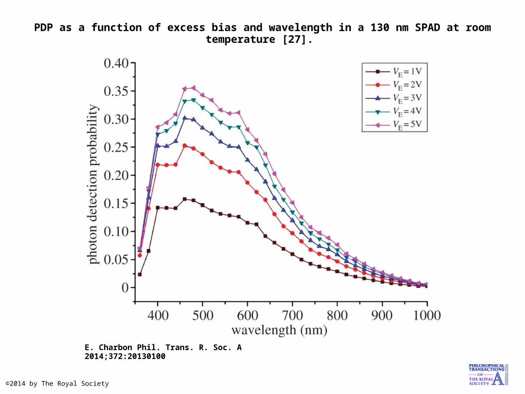
PDP as a function of excess bias and wavelength in a 130 nm SPAD at room temperature [27].
E. Charbon Phil. Trans. R. Soc. A 2014;372:20130100
©2014 by The Royal Society
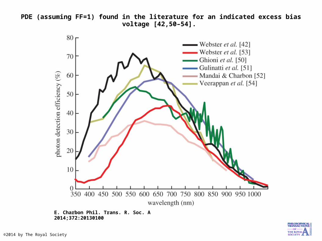
PDE (assuming FF=1) found in the literature for an indicated excess bias voltage [42,50–54].
E. Charbon Phil. Trans. R. Soc. A 2014;372:20130100
©2014 by The Royal Society
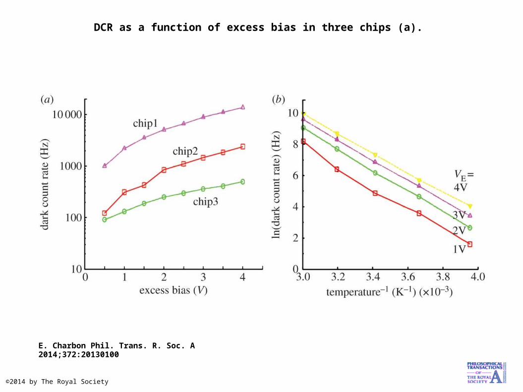
DCR as a function of excess bias in three chips (a).
E. Charbon Phil. Trans. R. Soc. A 2014;372:20130100
©2014 by The Royal Society
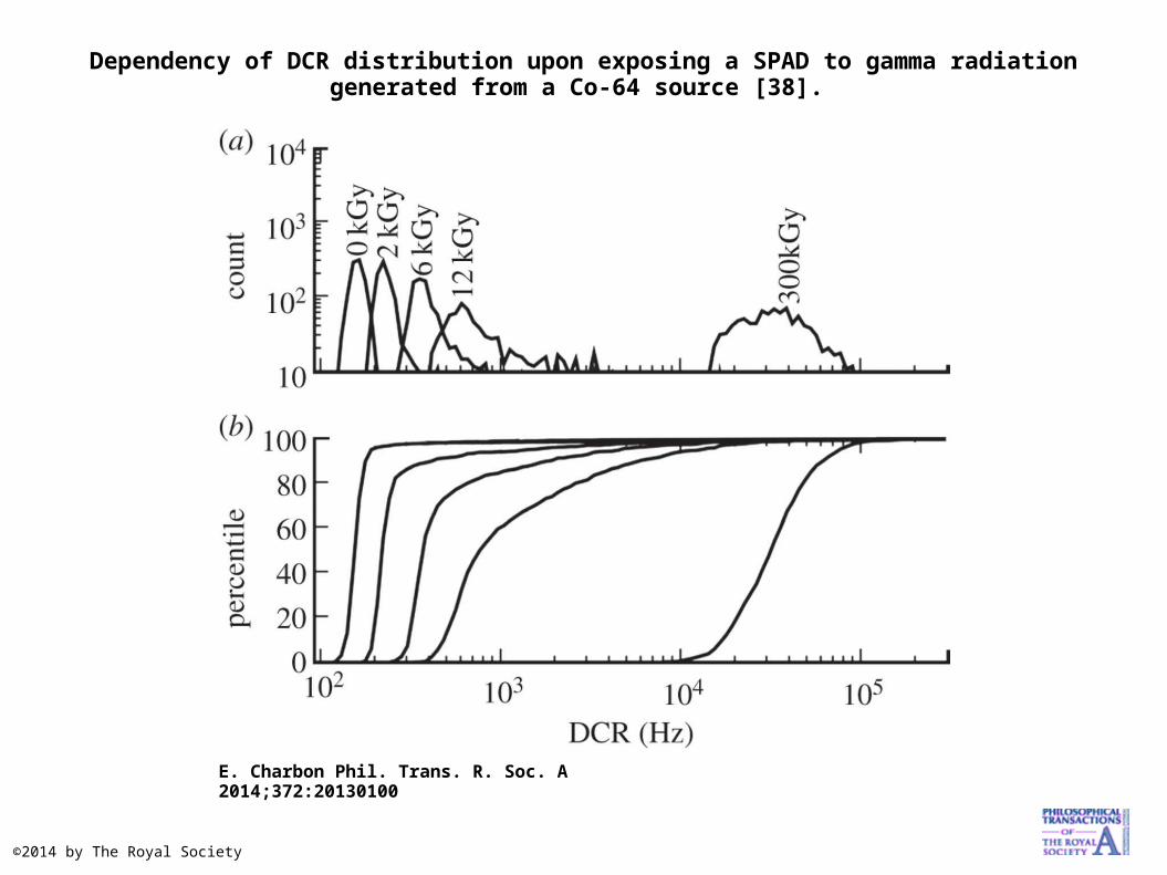
Dependency of DCR distribution upon exposing a SPAD to gamma radiation generated from a Co-64 source [38].
E. Charbon Phil. Trans. R. Soc. A 2014;372:20130100
©2014 by The Royal Society
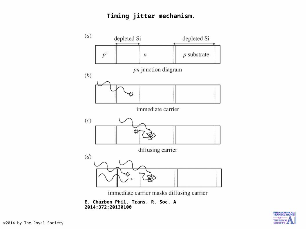
Timing jitter mechanism.
E. Charbon Phil. Trans. R. Soc. A 2014;372:20130100
©2014 by The Royal Society

Typical timing jitter response in a SPAD: (a) simulated and (b) measured response as a function of the number of detected photons n.
E. Charbon Phil. Trans. R. Soc. A 2014;372:20130100
©2014 by The Royal Society
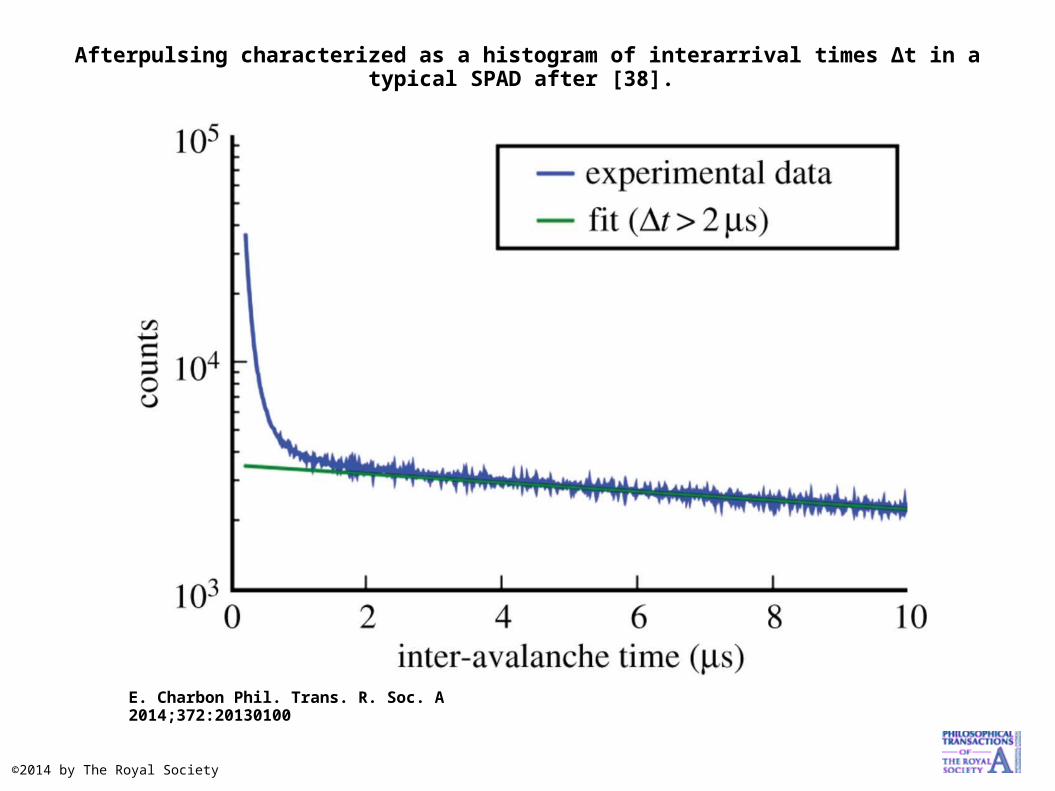
Afterpulsing characterized as a histogram of interarrival times Δt in a typical SPAD after [38].
E. Charbon Phil. Trans. R. Soc. A 2014;372:20130100
©2014 by The Royal Society
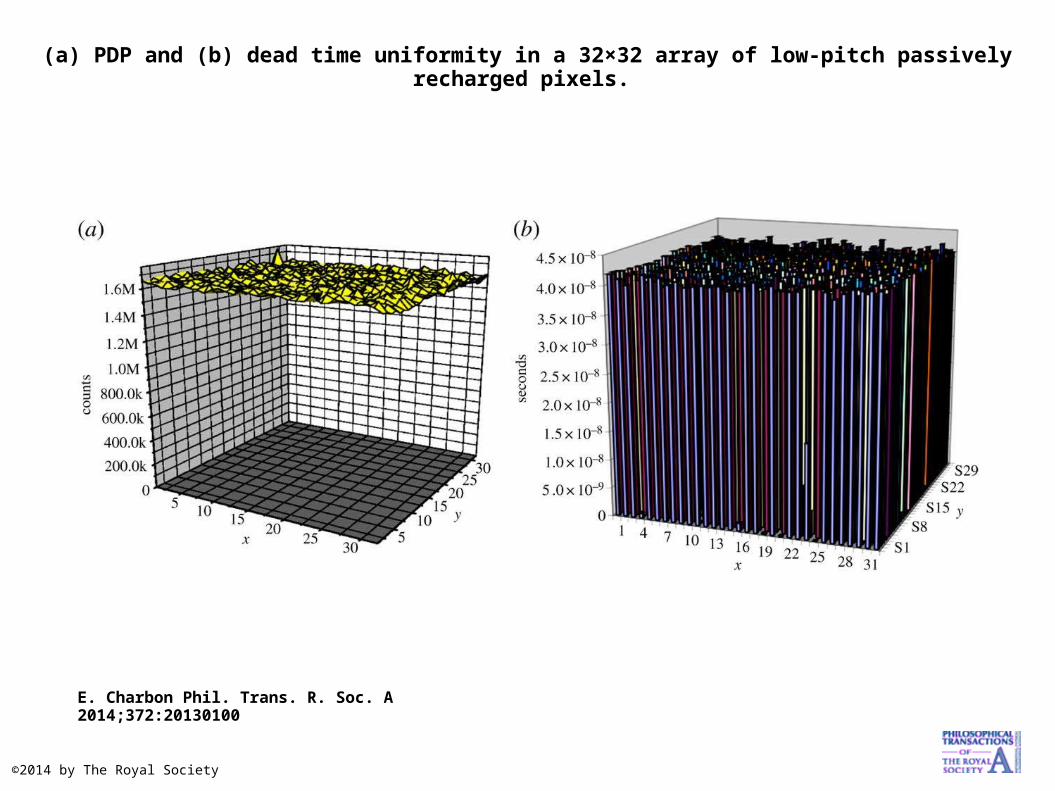
(a) PDP and (b) dead time uniformity in a 32×32 array of low-pitch passively recharged pixels.
E. Charbon Phil. Trans. R. Soc. A 2014;372:20130100
©2014 by The Royal Society
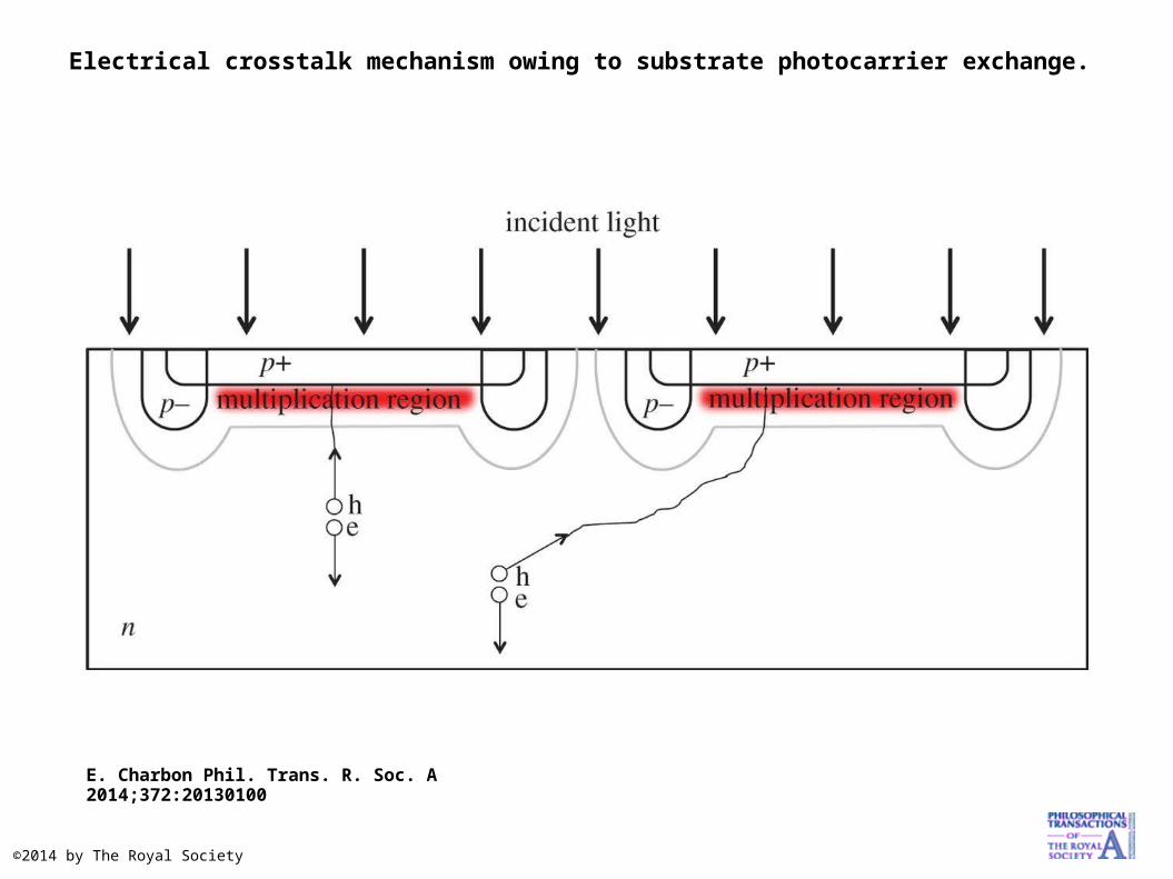
Electrical crosstalk mechanism owing to substrate photocarrier exchange.
E. Charbon Phil. Trans. R. Soc. A 2014;372:20130100
©2014 by The Royal Society

Crosstalk characterization around a high DCR pixel before (a) and after suppression of that pixel (b) [12].
E. Charbon Phil. Trans. R. Soc. A 2014;372:20130100
©2014 by The Royal Society
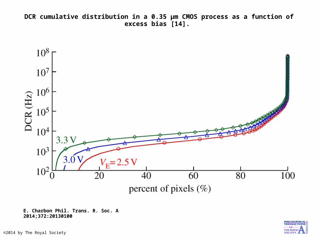
DCR cumulative distribution in a 0.35 μm CMOS process as a function of excess bias [14].
E. Charbon Phil. Trans. R. Soc. A 2014;372:20130100
©2014 by The Royal Society
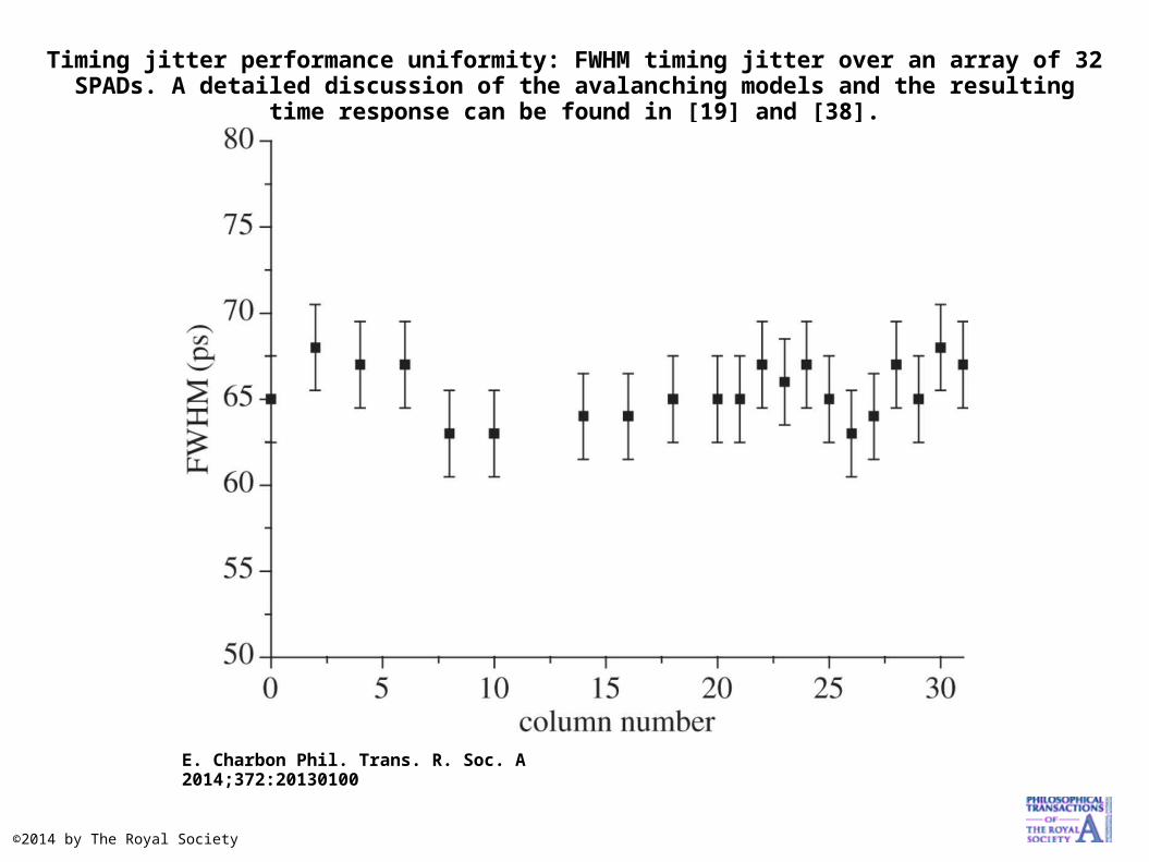
Timing jitter performance uniformity: FWHM timing jitter over an array of 32 SPADs. A detailed discussion of the avalanching models and the resulting time response can be found in [19]
and [38].
E. Charbon Phil. Trans. R. Soc. A 2014;372:20130100
©2014 by The Royal Society
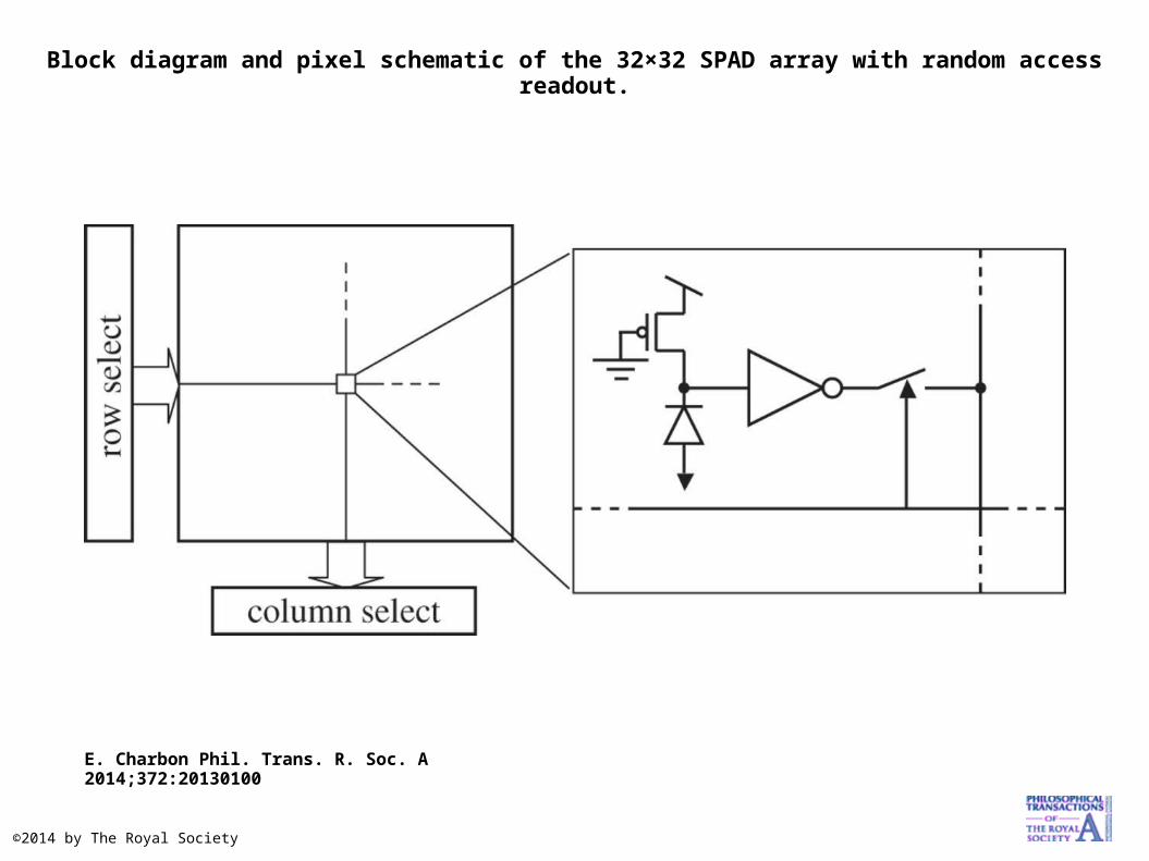
Block diagram and pixel schematic of the 32×32 SPAD array with random access readout.
E. Charbon Phil. Trans. R. Soc. A 2014;372:20130100
©2014 by The Royal Society

A 32×32 SPAD array with random access readout [5,22].
E. Charbon Phil. Trans. R. Soc. A 2014;372:20130100
©2014 by The Royal Society

Schematic diagram of the latchless pipelined readout (a); timing diagram and operation of the circuit (b).
E. Charbon Phil. Trans. R. Soc. A 2014;372:20130100
©2014 by The Royal Society
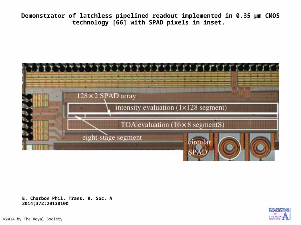
Demonstrator of latchless pipelined readout implemented in 0.35 μm CMOS technology [66] with SPAD pixels in inset.
E. Charbon Phil. Trans. R. Soc. A 2014;372:20130100
©2014 by The Royal Society
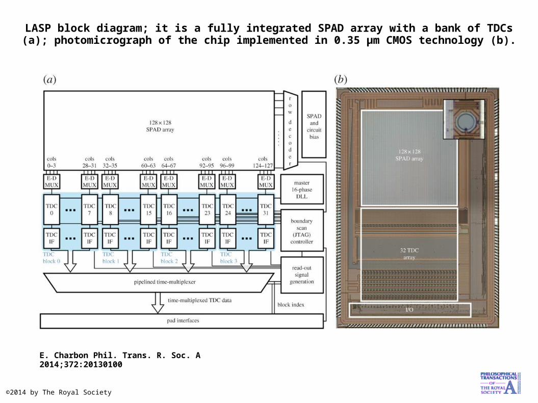
LASP block diagram; it is a fully integrated SPAD array with a bank of TDCs (a); photomicrograph of the chip implemented in 0.35 μm CMOS technology (b).
E. Charbon Phil. Trans. R. Soc. A 2014;372:20130100
©2014 by The Royal Society
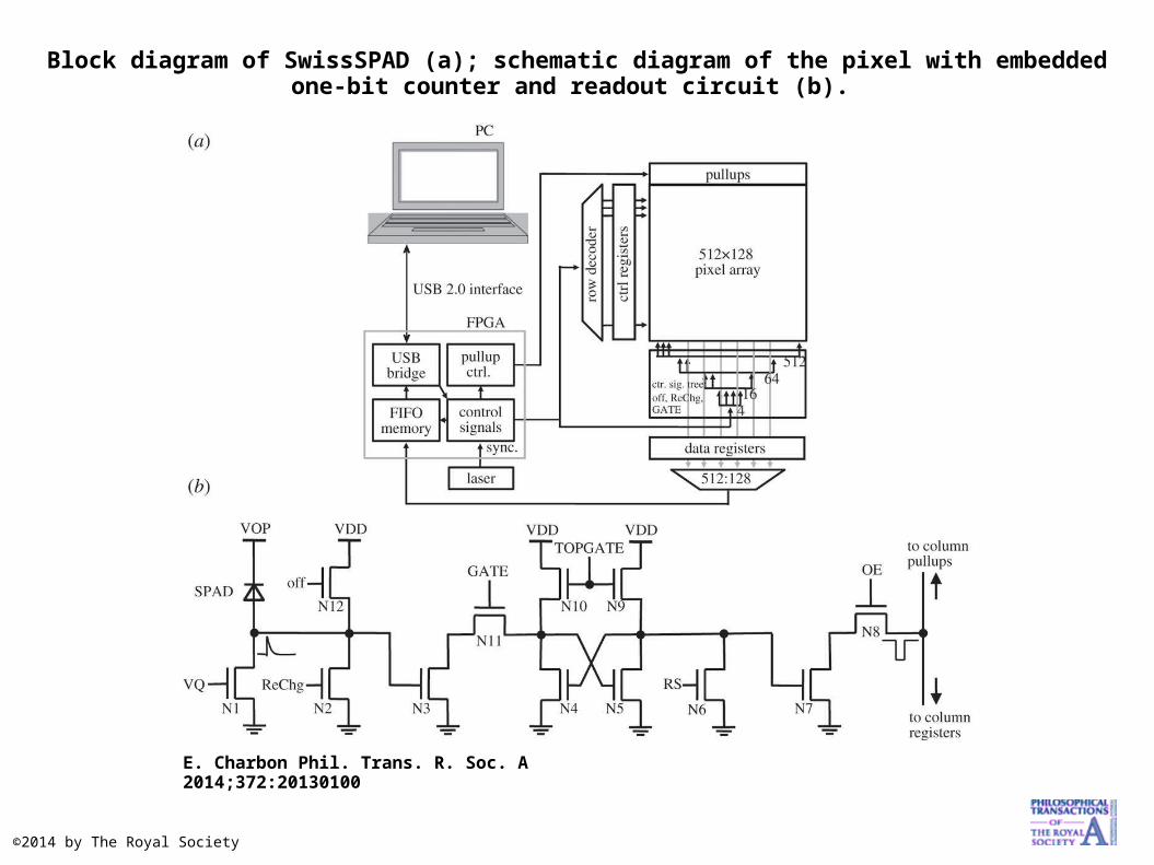
Block diagram of SwissSPAD (a); schematic diagram of the pixel with embedded one-bit counter and readout circuit (b).
E. Charbon Phil. Trans. R. Soc. A 2014;372:20130100
©2014 by The Royal Society
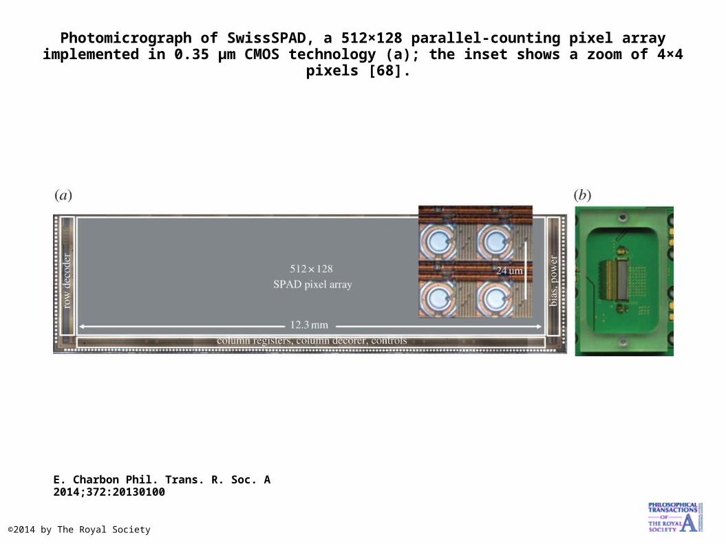
Photomicrograph of SwissSPAD, a 512×128 parallel-counting pixel array implemented in 0.35 μm CMOS technology (a); the inset shows a zoom of 4×4 pixels [68].
E. Charbon Phil. Trans. R. Soc. A 2014;372:20130100
©2014 by The Royal Society
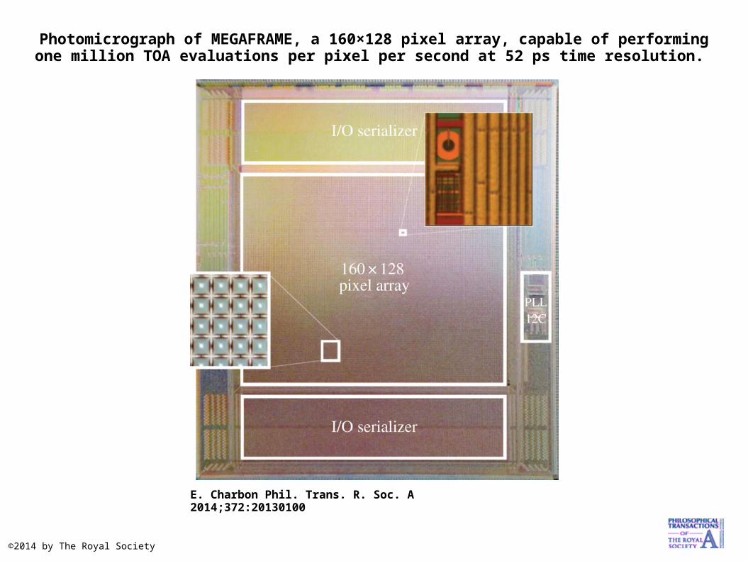
Photomicrograph of MEGAFRAME, a 160×128 pixel array, capable of performing one million TOA evaluations per pixel per second at 52 ps time resolution.
E. Charbon Phil. Trans. R. Soc. A 2014;372:20130100
©2014 by The Royal Society
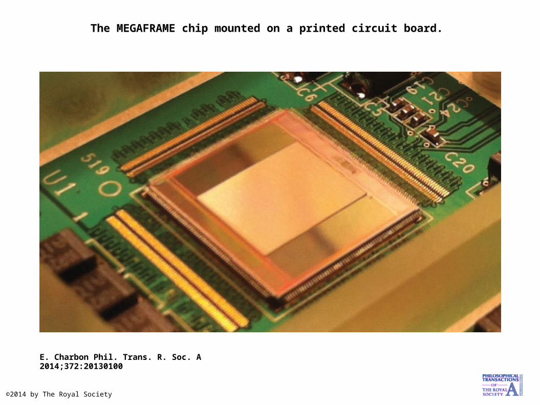
The MEGAFRAME chip mounted on a printed circuit board.
E. Charbon Phil. Trans. R. Soc. A 2014;372:20130100
©2014 by The Royal Society
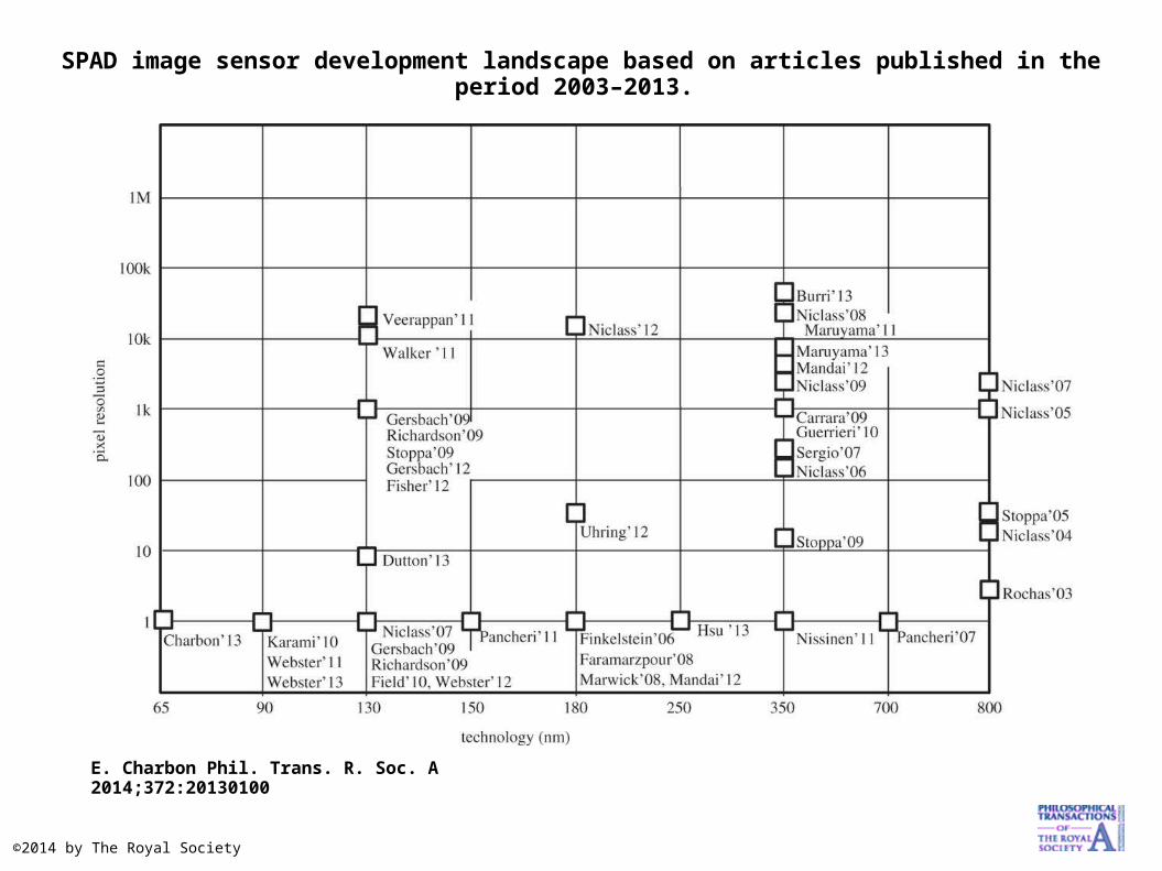
SPAD image sensor development landscape based on articles published in the period 2003–2013.
E. Charbon Phil. Trans. R. Soc. A 2014;372:20130100
©2014 by The Royal Society