simulation of yield / cost learning curves with y4
TRANSCRIPT

1
Simulation of Yield / Cost Learning Curves with Y4
Pranab K. Nag*, Wojciech Maly* and Hermann Jacobs**
*5000 Forbes AvenueDepartment of Electrical and Computer Engineering
Carnegie Mellon UniversityPittsburgh, PA 15213-3890
Phone: (412) - 268 - 4975 / 6637Fax: (412) - 268 - 3204
e-mail: {pkn, maly}@ece.cmu.edu
**Siemens AGDept. ZFE T ME 1
Corporate Research and Development, MicroelectronicsOtto Hahn Ring 6
D-81730 Munich, GermanyPhone: +49 89 636-45752
Fax: +49 89 636-47069e-mail: [email protected]
Abstract
This paper describes a prototype of a discrete event simulator - Y4 (Yield Forecaster) - capa-
ble of simulating defect related yield loss as a function of time, for a multi-product IC manu-
facturing line. The methodology of estimating yield and cost is based on mimicking the
operation and characteristics of a manufacturing line in the time domain. The paper presents
a set of models that take into account the effect of particles introduced during wafer process-
ing as well as changes in their densities due to process improvements. These models also
illustrate a possible way of accounting for the primary attributes of fabrication, product and
failure analysis which affect yield learning. A spectrum of results are presented for a manu-
facturing scenario to demonstrate the usefulness of the simulator in formulating IC manufac-
turing strategies.

2
1. Introduction
The cost of a new VLSI fabrication line producing several different products using several
hundred steps is now estimated to be close to a billion dollars. In the past years both cost and
complexity of manufacturing have been observed to increase exponentially and there has
been no indication that this trend is going to slow down [1]. This trend has been further fueled
by the need to produce faster, more complex and higher quality ICs, which demands precise
fabrication and a nearly particle-free environment. This upward trend places the industry at
an even higher risk. Thus, semiconductor manufacturers must be able to produce quality
products with minimum achievable cost to stay ahead of their competition.
Optimum exploration of cost-revenue trade-offs is difficult involving yield forecasts, and
cannot be realized unless it is based on adequate experimental or simulation models. A few
researchers have investigated yield learning in a semiconductor manufacturing line [2, 3, 4,
5], but the models applied do not capture the mechanics of yield learning itself. As a result,
methodologies to perform cost versus yield trade-off analysis over time do not exist at present.
To address this need, we have developed a new methodology to predict defect-related yield
which takes into consideration not only the operational aspects of manufacturing, but also the
process of yield learning. Models have been developed to estimate yield and cost as a function
of time. The goals of this paper are to present a tool -Y4 (Yield Forecaster) - which imple-
ments this methodology, and to illustrate Y4’s use in developing manufacturing strategies.
The structure of this paper is as follows. In the next section, we discuss the characteristics
of a modern manufacturing line, focussing on the yield learning process. In section 3 we derive
a methodology to simulate defect-related yield versus time curves for a manufacturing pro-
cess. Section 4 briefly deals with the implementation of the methodology and models imple-
mented in Y4. A spectrum of simulation results are presented in Section 5 to illustrate the
relevance of the cost and yield models applied.
2. Yield Learning in VLSI Fabrication
The new yield modeling philosophy postulated in this paper is based on the following ratio-
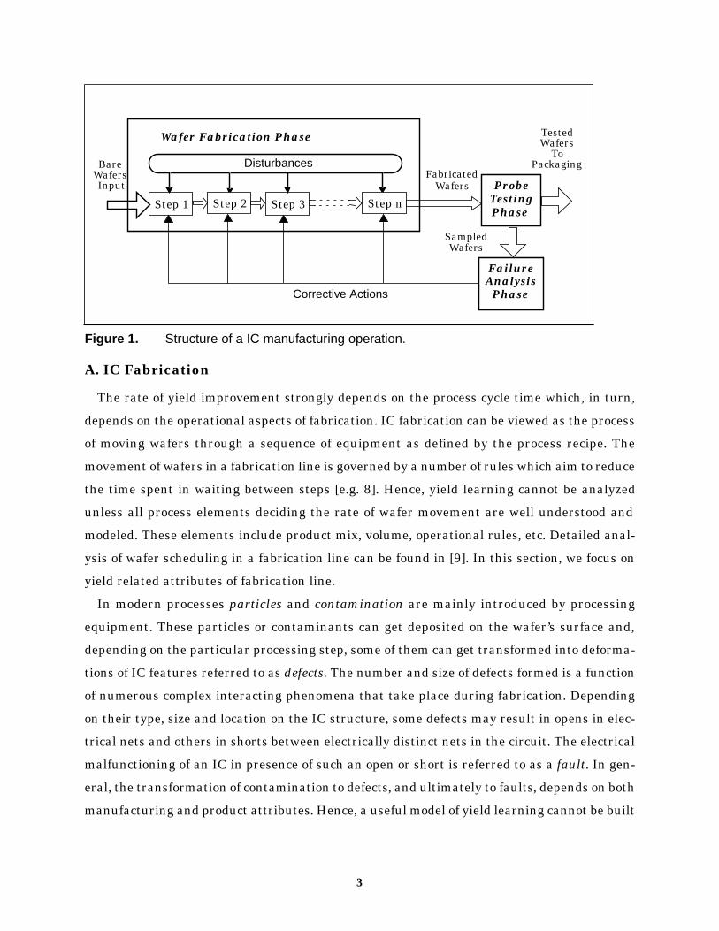
nale [6, 7]. A manufacturing process can be viewed as consisting of two components: product
fabrication and failure analysis, as illustrated in Figure 1. In order to capture the essence of
the mechanism of yield learning, it is necessary to take a closer look at the key events in each
of these components.
3
A. IC Fabrication
The rate of yield improvement strongly depends on the process cycle time which, in turn,
depends on the operational aspects of fabrication. IC fabrication can be viewed as the process
of moving wafers through a sequence of equipment as defined by the process recipe. The
movement of wafers in a fabrication line is governed by a number of rules which aim to reduce
the time spent in waiting between steps [e.g. 8]. Hence, yield learning cannot be analyzed
unless all process elements deciding the rate of wafer movement are well understood and
modeled. These elements include product mix, volume, operational rules, etc. Detailed anal-
ysis of wafer scheduling in a fabrication line can be found in [9]. In this section, we focus on
yield related attributes of fabrication line.
In modern processes particles and contamination are mainly introduced by processing
equipment. These particles or contaminants can get deposited on the wafer’s surface and,
depending on the particular processing step, some of them can get transformed into deforma-
tions of IC features referred to as defects. The number and size of defects formed is a function
of numerous complex interacting phenomena that take place during fabrication. Depending
on their type, size and location on the IC structure, some defects may result in opens in elec-
trical nets and others in shorts between electrically distinct nets in the circuit. The electrical
malfunctioning of an IC in presence of such an open or short is referred to as a fault. In gen-
eral, the transformation of contamination to defects, and ultimately to faults, depends on both
manufacturing and product attributes. Hence, a useful model of yield learning cannot be built
Figure 1. Structure of a IC manufacturing operation.
Step 1 Step 2 Step 3 Step n
Disturbances
Wafer Fabrication Phase
ProbeTesting
FailureAnalysisPhase
BareWafersInput
FabricatedWafers
TestedWafers
SampledWafers
Corrective Actions
Phase
ToPackaging

4
without an adequate understanding of the major mechanism of contamination deposition and
the associated contamination-defect-fault relationship [10].
B. Failure Analysis
Typically, improvement of process quality, i.e. yield increase, is achieved in two different
ways. One is contamination control and the other is via failure analysis. In this paper we focus
on the latter. For failure analysis, a small fraction of wafers are selected (after probe testing)
using some sampling rules. A simple sampling rule is, for instance, to select the wafer with
the highest number of failed ICs. More complex sampling rules can be used when more infor-
mation on the nature of the failure can be extracted from the electrical testing results.
Once a set of defective die is chosen, an attempt is made to diagnose the cause of failure in
each selected die. Diagnosis is usually formulated by performing defect localization and iden-
tification, analysis of the particle causing the defect, and identifying the set of equipment
which could be the possible source of the particle. Of these, the first step is the most time con-
suming and uncertain. The particle analysis step can also be time-consuming and require
very expensive equipment.
Defect localization is accomplished through direct observation methods such as optical,
scanning electron, and transmission electron microscopy [11, 12]. These methods, however,
have several drawbacks. First, these techniques are useful only when the portion of the die
which needs to be searched is fairly small. Second, defects which are in lower layers of the IC
(polysilicon for example) may be masked by the upper levels. Use of diagnostic testing to
obtain tighter bounds on the neighborhood of the defects [15] is very promising and in the
future may vastly improve defect localization.
Once a defect is localized, one can usually identify the step which introduced the particle
causing the defect. In cases where this is not possible, more elaborate techniques (such as
scanning electron microscopy (SEM) [13], selectively stripping away IC layers [14], or cross-
section analysis using TEM) can be used to identify the nature or chemical composition of the
particle.
The step that follows failure analysis is that of taking corrective actions. Observe, however,
from a yield learning perspective, corrective actions are justifiable if a significant number of
defects of the same type are detected. Only then must the suspect piece of equipment be
cleaned or repaired, or process modifications be applied.

5
3. Modeling the Yield Learning Process
From the above short summary, it is evident that the yield learning process should be
described as a sequence of events starting with the introduction of particles, followed by
detection of defects and identification of their source, and concluding with eliminating the
source of particles. The rate of yield learning, therefore, depends on:
1. The relationship between particles, defects and faults;
2. Ease of defect localization which in turn depends on:
a. size, layer and type of defect,
b. level of “diagnosability” of the IC design and,
c. probability of occurrence of catastrophic defects;
3. Effectiveness of the corrective actions performed;
4. The timing of each of the events mentioned above;
5. Rate of wafer movement through the process.
All of the above factors must be modeled in order to build an yield learning simulator.
In order to describe the yield as a function of time, let us first concentrate on a single prod-
uct manufacturing line. Let us also assume that there exists only one type of defect originat-
ing from a single source (a piece of equipment) of particles. This simple case suffices to capture
the essence of the yield learning process.
The hypothetical yield versus time curve for the above scenario resembles the staircase
function shown in Figure 2. Here, Tf is the time required for analysis and detection of the fail-
ure mechanism leading to process intervention. Te is the time needed for a process correction
which decreases contamination levels, and the time required for the new process parameters
to be effective. Tr is the interval between the time process correction is made and the time
change in yield of the fabricated wafers is observed. The total time required for yield change
to occur is Tc = (Tf + Te + Tr) and the net change in yield is Yc. The value of Yc is determined
by the new level of contamination.
Estimating Tr is equivalent to estimating the cycle time for a process, albeit partially, start-
ing from an intermediate process step where the correction is made until the last step of the
process. Thus, it is the sum of the raw processing time (RPT) and the queuing time that
results when wafers must wait between process steps. One of the major contributors to the
queuing time is the downtime of the equipment. Note that the time factor Te may also con-

6
tribute to the equipment downtime depending on the outcome of failure analysis. Tf, the time
needed to detect and localize the defect, depends on a number of attributes associated with
IC design, defect and failure analysis process. The change in yield, Yc, on the other hand,
depends on the correctness of the diagnosis and the efficiency with which the contamination
rate can be reduced as a result of the corrective actions.
Note that Figure 2 depicts yield improvement cycles for only one type of defect originating
from one source. In reality, there will be a number of such cycles overlapping in time with each
other. The yield learning curve for a product is, thus, a combination of all such individual
overlapping learning curves.
From this basic model of the yield learning process, it is clear that the primary capability
of the simulator must be to keep track of the sequence of events in a factory [e.g. 16]. The sec-
ond requirement for the simulator is the ability to simulate the movement of the wafers in a
fabrication line, and representing such entities as product, process recipes, equipment, per-
sonnel and operating rules. The specific modeling aspects have been dealt with in detail by
others [9, 16] with the exception of models for evaluating Tf and Yc. Further, to achieve the
capability of performing cost revenue trade-off studies, the simulator must be able to take into
account the capital and the operating costs of the fabrication line and failure analysis facility.
Ceratin key aspects of modeling yield loss, failure analysis, corrective actions and cost are dis-
cussed next.
Figure 2. Key events in yield learning process.
Yie
ld
Time
Tc
Tf Te Tr
Yc
Tc
Tf Te Tr
Yc
SamplingTime
ProcessIntervention
ParametersModified
YieldChange
Observed

7
A. Yield Modeling
The primary aim in yield modeling is to classify each die on a wafer as fault-free or faulty
so that yield can easily be estimated by evaluating the ratio of good die to the total number
of die on a wafer. One can simulate yield in a Monte Carlo manner but for reasons of practi-
cality it is necessary to develop simpler models suitable for an event driven system.
In attempting to develop a simpler yield model, the first step is to choose a model for the
particles that may ultimately cause IC failure. We assume that particle types are uniquely
characterized and associated with their source i.e. the generating equipment (however, each
source can generate more than one type of particle and several sources can generate the same
type of particle). A source and particle type pair will be referred to as a disturbance type. In
the simulator described in this paper, each disturbance type is assumed to generate two or
three dimensional particles of a certain size, Rc, and the number of particles on a wafer is
given by Nc. The distributions of Nc and Rc are assumed to be independent of each other and
modeled as gaussian and polynomial distributions, respectively [17, 18]. The particular form
of polynomial distribution for defect size is K/Rp, where K is a constant, R, the defect size and,
p, the exponent is extracted experimentally [18]. It is also assumed that the particles are dis-
tributed uniformly on a wafer.
The next important modeling issue is the contamination-defect-fault relationship. This
relationship is modeled in two steps - modeling the transformation of contamination to defect
and then defect to fault. In modeling particle to defect transformation, one has to consider pos-
sible changes in defect size. If the particle size is Rc, then the defect size, Rd is given by Rd =
CcRc, where Cc is a given constant for a given process step. Defect to defect transformation
(three dimensional defect propagation) and removal of defects (due to layer polishing, wafer
cleaning, etc.) are modeled in a similar manner.
Defect to fault mapping has been extensively studied in the past. There are two distinct
methods, one uses Monte Carlo techniques [19] and the other uses models based upon the crit-
ical area concept [20, 21]. Monte Carlo techniques are excessively time-consuming, whereas
models based on critical area estimate only the average yield. Neither method directly
answers the question: given the size, location and layer of a defect on a wafer, what is the
resulting fault, if any? We have used a variation of the critical area concept which is described
in detail in [7]. It is based on the fact that if defects are assumed to be uniformly distributed,
then one can avoid assigning a location to the defects (which can increase the computational
complexity). Instead, one can assign a probability that a defect is located inside the critical

8
area for that defect and a fault type. An important feature of this concept is its ability to
model, with high accuracy, the sensitivity of a layout design to various kinds of defects.
B. Modeling Failure Analysis Process
In modeling the failure analysis process, the objective is to estimate the time required to
identify a subset of equipment responsible for causing a die to be defective. Here, we present
some of the key features of such a model.
Failure analysis is modeled as a three step process involving sampling of wafers, multi-step
defect analysis and assignment of the dominant cause of failure. In the sampling step, those
wafers are selected for analysis that have at least a given number of defective die. To avoid
overloading of failure analysis equipment, the above rule is combined with the requirement
that wafers can be sampled only when the number of wafers in the input queue of failure anal-
ysis is less than a certain given value. Hence, timing of wafer selection is a function of the rate
of wafer movement (through fabrication steps) and the level of wafer defectivity.
We are assuming in this paper that defect analysis may require a multi-step procedure. To
estimate the time required at each step of the defect analysis process, it is useful to introduce
a diagnosability measure, m, with a value between 0.0 and 1.0 defined for type of fault in each
product. (A value close to 1.0 indicates that the fault is easily diagnosable). Suppose that at
each step, starting with an initial value of mi, a final value of mf is achieved in time tf. One
possible form of the function is given by:
(1)
where ed represents the efficiency of the diagnosis process and is a parameter which depends
on the analysis equipment. The above model of the diagnostic process implies that more the
time spent on analysis, the higher are the chances of detecting the cause of the fault.
It remains now to define a model for estimating the initial diagnosability for the first step
of the analysis. It is assumed that each fault for a product is characterized by:
1. An estimate for the area on the chip where the defect may be present, As (The maxi-
mum value for As is Achip or the total area of the chip).
2. The size of the defect, R.
3. The layer n, in which the defect is manifested, n = 0 for the top layer.
mf 1.0 1.0 mi–( )eedtf–
–=

9
Using these parameters one can estimate the initial diagnosability by the following equation:
(2)
where a, b, and c are positive constants which capture the relative importance of each of the
three attributes defined above. This model also provides the ability to capture differences in
products which are affected by the same kind of defects. However, the model implicitly
assumes that the source is correctly identified in the event that the diagnosis is successful. In
reality, however, diagnosis can be incorrect introduced by ambiguity and/or lack of
information. In fact, correct diagnosis may itself take several learning cycles. Ambiguity
arises from the fact that many different sources of particles may cause the same defect or
result in the same faulty signature. Thus, this can be taken into account by properly
formulating the particle to defect to fault mapping information. Likewise, incorrect
information can be modeled by introducing false mapping information.
Another component of defect analysis time is the queuing time which is governed by equip-
ment availability and the scheduling rules applied to control wafer flow. We assume a first-in-
first-out rule. Further, a maximum time limit for analysis is also assumed in order to avoid
long waiting times for incoming wafers. In reality, queuing times can be long because of high
priority wafers or other operational reasons.
C. Modeling Corrective Actions
The main objectives in modeling corrective actions are to:
a. decide when a piece of equipment needs to be repaired or cleaned,
b. decide when the equipment can be taken off-line (if required), and
c. estimate the new value of parameters modifying particle generation model.
The first requirement can be achieved by keeping a count, Esuspect, of the number of times a
piece of equipment is held responsible for a fault in the die fabricated. Note that several
equipment can be held responsible simultaneously. When the count exceeds a predefined
threshold, Ethresh, the particular piece of equipment needs to be cleaned. The second
requirement is met by using the rule to wait for the next scheduled maintenance period to
perform the cleaning operation if the estimated waiting time is less than a predefined interval
of time.
mi 1 a n⋅–( ) 1 b As⋅ c As R⋅ ⋅+–( )=

10
Modeling considerations for the third and most important factor - the change in model
parameters of particles must be discussed in more detail. In our approach it is assumed that
both the number of particles per wafer and the relative occurrences of different particle sizes
change as a result of cleaning. It is further assumed that the new distribution of the number
of particles, Nc, is a normal distribution with a new mean, mnew, and standard deviation, σnew,
given by:
(3)
where km and kσ are given constants between 0.0 and 1.0. A value of zero indicates that the
operation of cleaning removes the source entirely. Similarly, we assume that the distribution
of particle size, Rc, is still a polynomial distribution with new exponent, pnew, given by:
(4)
where pdiff is a positive constant. This model implies that a change in particle number is
independent of any change in size distribution. The other important assumption in our model
is that cleaning or repairing changes particle (by a fixed factor) characteristics so as to
continuously reduce the rate of occurrence of defective die. Any increase in particle count with
time can be taken into account by modifying the particle model by adding a time component.
Also, it is quite likely that actual change in particle characteristics itself may be a randomly
varying quantity.
In the above modeling consideration we have ignored the fact that often instead of equip-
ment, process steps or materials used in a step may be held responsible for defects. A simple
variation of the above model can be used to model application of corrective action to process
steps. Difference will arise in the time taken to make the correction.
D. Cost Modeling
One of the accepted industry standards for estimating manufacturing cost is the cost-of-
ownership model developed by Sematech [22]. In this model, the focus is on estimating the
effective contribution of equipment and other resources to the wafer cost. This analytical
model requires prior estimates of attributes like uptime, throughput yield, die yield, cycle
times, etc. These parameters could be extracted by direct observation in a factory with vary-
ing degree of confidence, but cannot easily be extrapolated to an alternate scenario. The cost
mnew mold km⋅=
σnew σold kσ⋅=
pnew pold pdiff+=

11
model described in [23] gives a direct estimate of wafer cost arising out of equipment usage
(activity) in a multi-product fabrication line. In that model wafer cost is defined as being com-
posed of two components: the first being the direct equipment usage (based on active usage of
equipment by a given product) and the fraction of time during which a piece of equipment is
not processing any wafers. The focus is on "fair" allocation of the cost incurred when equip-
ment is not processing any wafers in a multi-product facility. Costs arising out of material/
energy usage, equipment service and operators are also taken into account. In this paper, we
use a variation of the model to estimate the wafer cost and then combine the wafer cost with
the wafer yield estimates to model the die cost [24].
4. Structure and Implementation of Y4
The methodology and the models for yield learning described in the previous section have
been implemented as a software tool called Y4 (Yield Forecaster). Figure 3 shows the overall
structure of the Y4 framework. The heart of the simulator is the event handler which com-
municates with six modules: the wafer movement simulator (WSIM), the yield simulator
(YSIM), the failure analysis simulator (FASIM), the in-line particle monitor simulator
(PSIM), the cost simulator (COSIM) and the probe tester simulator (TSIM). The operation of
the event handler and these six modules can be controlled through the simulation control
unit. The user can implement different models using the toolkit of functions provided for
accessing and modifying the common database for all the modules and the event handling
routines. A basic user interface is available to read input files for the models, output the sta-
tistics gathered and customize the simulation control strategy.
The models described in the previous section have been implemented as internal models of
the submodules (WSIM, etc.). WSIM is similar to the commercial fabrication line simulator
ManSim [25], although the current implementation models only a subset of ManSim’s oper-
ating rules and conditions. On the other hand, the number of external events that can be
defined in ManSim is limited. Thus, it was considered necessary to implement Y4 with the
ability to define events for particle introduction (YSIM), failure analysis (FASIM) and correc-
tive actions (YSIM).
Discussion of the models for particle monitor simulation (PSIM) and the wafer test simula-
tion (TSIM) are outside the scope of this paper. A description of the models and the results
obtained are presented in [7]. In this paper, we focus on the other four submodules - WSIM,
YSIM, FASIM and COSIM.

12
5. Illustrative Simulation Results
In this section, two kinds of results are presented. First, results of simulations replicating
some of the known phenomena in a manufacturing line are described. Cycle times and
throughput analyses of a single and a two product manufacturing line are presented. Subse-
quent simulation results illustrate the general difference in wafer cost for single and two
product factories. These examples illustrate the basic functionality of Y4. Then, illustration
of capability to handle non-trivial trade-offs are presented through yield learning simula-
tions. The impact of the capacity of the failure analysis facility on the learning rate is pre-
sented. The impact on cost of a sudden degradation in yield caused by a sharp increase in
particle rates in one piece of equipment is analyzed. Finally, we consider the impact of ease
of diagnosability of a product on the yield learning rate.
The minimum duration of simulation in each case is one year with a 12 week warm-up
period. The process recipes, equipment, and cost data used in these examples were taken from
an existing manufacturing line. Operators in the manufacturing line were not simulated, and
thus, any variability in observed cycle times and cost is solely due to the temporary unavail-
ability of equipment.
Figure 3. Top level structure of the Y4 framework.
Event Handler
WSIM YSIM
PSIM
FASIM
TSIM
COSIM
CREST Layout
Databaseand
Toolkit
SimulationControl
User Models
DataInput/Output
User Interface
OutputFiles
InputFiles
Y4 Core

13
In the examples that follow, we will primarily use a 0.5 micron 3 metal CMOS process rec-
ipe. Due to its proprietary nature, data pertaining to cost of equipment, etc., has been scaled
appropriately. The process recipes had to be reduced for the same reason. The modified recipe
consists of 145 steps using 183 pieces of equipment for a 2496 wafer starts per week (WSPW)
capacity factory (a medium sized factory). The lot size is 24 wafers and thus the line capacity
is 104 lots per week. In a few examples, we will also use a 0.5 micron, 2-metal, trench capac-
itor DRAM process. After preprocessing, the recipe for this process consists of 175 steps using
214 pieces of equipment also with a capacity of 2496 WSPW. The raw processing times are
302 hrs and 427 hrs for the CMOS and DRAM processes, respectively. All of the above pro-
cesses and cost data are good approximations of medium size real life manufacturing opera-
tions.
A. Cycle Time Simulation
14
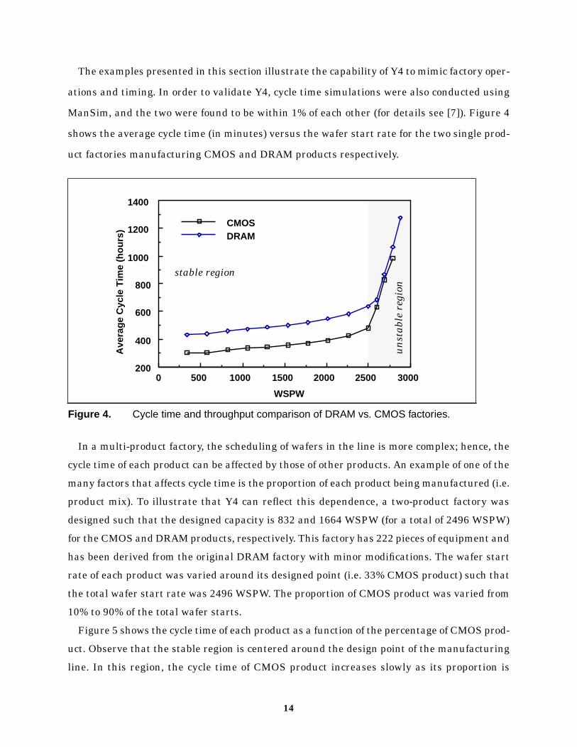
The examples presented in this section illustrate the capability of Y4 to mimic factory oper-
ations and timing. In order to validate Y4, cycle time simulations were also conducted using
ManSim, and the two were found to be within 1% of each other (for details see [7]). Figure 4
shows the average cycle time (in minutes) versus the wafer start rate for the two single prod-
uct factories manufacturing CMOS and DRAM products respectively.
In a multi-product factory, the scheduling of wafers in the line is more complex; hence, the
cycle time of each product can be affected by those of other products. An example of one of the
many factors that affects cycle time is the proportion of each product being manufactured (i.e.
product mix). To illustrate that Y4 can reflect this dependence, a two-product factory was
designed such that the designed capacity is 832 and 1664 WSPW (for a total of 2496 WSPW)
for the CMOS and DRAM products, respectively. This factory has 222 pieces of equipment and
has been derived from the original DRAM factory with minor modifications. The wafer start
rate of each product was varied around its designed point (i.e. 33% CMOS product) such that
the total wafer start rate was 2496 WSPW. The proportion of CMOS product was varied from
10% to 90% of the total wafer starts.
Figure 5 shows the cycle time of each product as a function of the percentage of CMOS prod-
uct. Observe that the stable region is centered around the design point of the manufacturing
line. In this region, the cycle time of CMOS product increases slowly as its proportion is
Figure 4. Cycle time and throughput comparison of DRAM vs. CMOS factories.
300025002000150010005000200
400
600
800
1000
1200
1400
CMOSDRAM
WSPW
Ave
rage
Cyc
le T
ime
(hou
rs)
stable region
un
stab
le r
egio
n

15
increased. The cycle time of DRAM product, on the other hand, decreases slowly in this range.
Since this factory is derived from the DRAM line, the characteristics of the line are dominated
by the DRAM process. Hence, the cycle time of the CMOS product increases as its proportion
is raised. In the unstable region, cycle times of both products increase rapidly since the avail-
able capacity is not enough to fabricate the larger proportion of CMOS product in the line. In
general, one can expect to encounter unstable operating conditions on both extremes around
the design point.
B. Cost Analysis of Fabrication Line
In this section, results of wafer cost estimates are presented for the manufacturing lines
described in the previous section. For the CMOS factory, the minimum value of wafer cost
attained is $2745 (at designed capacity). For the DRAM product, the minimum wafer cost
obtained is $3272. The DRAM cost is higher mainly because the process requires expensive
equipment to define the trench capacitors and executes more lithography steps.
Figure 6 shows estimates of wafer cost as a function of the product mix for the two-product
factory presented earlier. Increasing the proportion of CMOS product decreases its cost for
the same reason as in a single product factory - better utilization of the capacity for the equip-
ment used in the CMOS process. Further, the cost incurred due to the idle times of equipment
used solely by one process is allocated to the corresponding product only - an artifact of the
Figure 5. Cycle time of two product factory (CMOS and DRAM).
% of CMOS product
Ave
rage
Cyc
le T
ime
(hou
rs)
1009080706050403020100500
600
700
800
900
1000
1100
CMOSDRAM
stable region
unstable region

16
“fair” allocation cost model. This effect is more pronounced for the DRAM product since it
requires specialized equipment (for trench capacitors and epitaxial layers) not required by
the CMOS process.
In the unstable operating region, the wafer cost for both products increases as the propor-
tion of CMOS product is increased. The cost of CMOS product increases because of starvation
of non-bottleneck equipment in spite of the fact that more wafers are being produced. In fact,
the throughput of the CMOS product is no longer directly proportional to the input wafer
start rate as one may expect. The cost of DRAM product, on the other hand, increases dra-
matically mainly because of under-utilization of the “DRAM only” dedicated equipment.
Notice that a similar effect is not apparent for the CMOS product at low wafer starts since
the CMOS process does not have any significant (expensive) equipment dedicated to it.
Almost all the process steps of CMOS are shared by the DRAM process leading to nearly uni-
form utilization of the shared equipment.
C. Yield Learning Analysis
In order to illustrate the capability of Y4 to simulate yield learning curves, the fabrication
line for the 0.5 micron 3 metal CMOS process was used. It was assumed that wafers are 6
inches in diameter which can accommodate 110 chips of 1.4 cm2 size each.
Defects in the polysilicon and the three metal layers were considered as main yield detrac-
tors. Defects in the polysilicon layer were assumed to be introduced during the poly deposition
Figure 6. Wafer cost as a function of product mix.
10090807060504030201002000
2500
3000
3500
4000
4500
5000
5500
6000
6500
7000CMOSDRAM
% of CMOS product
Cos
t of W
afer
($) stable region
unstable region
design point

17
step. Defects in metal layers were assumed to be caused by particles generated at the common
sputtering step. It was also assumed that these defects result in shorts in their respective lay-
ers. The critical area for shorts, as a function of defect size, for each defect type was derived
by scaling results obtained from several CMOS designs in order to mimic a microprocessor
like product [21].
The initial exponent, p, of the particle size distribution was taken to be 2.0. The initial mean
and variance of the particle number distribution was set in a such a way that the total initial
yield was less than 10%. Note that the initial yield also depends on the critical areas assumed
for each of the defect types.
Wafers were sampled for failure analysis when there were more than 30 defective die on a
wafer and when there were fewer than 3 wafers waiting to be analyzed. The failure analysis
was simulated as comprising five steps: observation under microscope, observation with
SEM, stripping layers (if required), cross section analysis and spectroscopic analysis (Wave-
length Dispersion Spectroscopy -WDX, Energy Dispersion Spectroscopy - EDX, etc.). These
steps were carried out in sequence and the time required at each step was calculated using
Eqns. 1 and 2. The parameter ed for each equipment was chosen to reflect the time expected
to be spent at each of these steps. The maximum time required to analyze 30 defects in the
top metal layer was about 2 weeks (not considering the queueing time). The value of search
area, As (Eq. 2), for each product under consideration was assumed to be defined by a distri-
bution given as a table ranging from 0.0 to 1.4 cm2 (chip size) with a mean at 0.2 cm2.
Assignment of the equipment responsible was accomplished by incrementing the variable
Esuspect by 1 for the piece of equipment responsible for the defect. For the rest of the equiva-
lent equipment, the increment value was 0.5. Corrective actions on a piece of equipment were
deemed necessary when this count exceeded 20 (Ethresh). The equipment was taken off-line
for cleaning as soon as it had finished processing the current lot of wafers. The value of pdiff
was set to be 0.02 for each type of particle, and km and kσ (Eq. 3) were set to be 0.95.
Figure 7 shows an example of the trend plot of total die yield for each lot. Note that the yield
starts increasing only after about 15 weeks. This is because failure analysis is not conducted
for the first 10 weeks in order to let the simulated fabrication line settle into an equilibrium.
The total period of simulation is 75 weeks and the yield values shown in the figure are for
approximately 7500 lots. Note that yield learning rate is quite high. This is because only four
types of defects are considered and that the failure analysis turnaround time is relatively
quick (an artifact of simple FIFO scheduling rule used).

18
The variance in yield is observed to increase (Figure 7) as the yield ramps up and then
decreases as the rate of yield increase drops. This reflects the variance of a binomial distribu-
tion which is highest when yield is 0.5 (i.e. variance = npq, where, n is the number of samples,
p is probability that a die is good and q = 1-p). This is because the probability of occurrence of
a defective die on a wafer is nearly constant in a short period of time and thus the total num-
ber of defective die on a wafer must follow a binomial distribution. In reality, the variance in
yield is likely to be much larger than the value predicted by our model because of noise in
other process parameters (like etch rate, film thickness, etc.). Such factors are not currently
modeled in Y4.
The weekly average of the yield trend plot is shown in Figure 8 along with the yield of the
poly-silicon and the metal 3 layers. Observe that the yield of the metal 3 layer starts to
increase almost right after failure analysis is initiated (after the 10th week). The polysilicon
layer yield, on the other hand, starts to increase only after another 15 weeks (around 25th
week). This reflects the fact that polysilicon defects are more difficult to detect than metal 3
defects which are nearer to the surface of the chip. Further, the yield of metal 3 is low enough
in the first few weeks of failure analysis that the resources are kept busy analyzing samples
for metal defects. Polysilicon defects are, in effect, ignored until the metal 3 yield reaches
about 0.65. However the rate of yield learning for the polysilicon layer is higher than metal 3
since the increased availability of samples with polysilicon defects compensates for the
decreased diagnosability of these defects.
Figure 7. Example of simulated yield learning curve.
Yie
ld
Week
0
0.1
0.2
0.3
0.4
0.5
0.6
0.7
0.8
0.9
0 10 20 30 40 50 60 70 80
war
m-u
p pe
riod

19
Figure 9 shows the results of yield simulation when the number of each type of failure anal-
ysis equipment is doubled. In addition to the obvious increase in the yield learning, two more
effects are apparent. First, the polysilicon layer yield starts to increase around the 20th week,
which is about 5 weeks sooner than in the previous case. Secondly, at this point, the metal 3
yield is higher than that in the earlier case (0.73 instead of 0.65). There is enough leftover
capacity to allow for allocation of resources to the detection of polysilicon defects while the
metal defects are being analyzed. Availability of more resources enables metal defects to be
diagnosed more quickly.
D. Impact of Sudden Change in Yield on Learning Rate and Cost
In the previous section, we have implicitly assumed that changes occurring in particle rates
and size distributions due to cleaning the corresponding equipment causes an improvement
in yield. However, they may possibly change in such a way as to degrade the yield. This could
be due to some internal disturbance such as imprecise processing causing more particles to
be released. Here, we consider the result of such a change occurring in one of the sputtering
tools. The change causes the metal yield to degrade. Specifically, at the end of 30th week, the
mean of the particle number distribution for one of the seven sputtering tools is assumed to
increase by a factor of five.
Figure 10 shows the result of the simulation illustrating the yield trend plots. Observe that
the net yield learning rate has decreased compared to the result shown in Figure 8. The
Figure 8. Yield learning curves for CMOS product.
807060504030201000.0
0.1
0.2
0.3
0.4
0.5
0.6
0.7
0.8
0.9
1.0
Total yieldPoly yieldMetal 3 yield
Week
Yie
ld

20
increase in metal defects causes metal yield to drop first. After a certain delay, failure analy-
sis catches up with the increased number of defective die with metal defects, and metal yield
starts to increase again. But at the same time, the polysilicon yield learning rate drops
because failure analysis resources are mostly consumed in detecting metal defects.
Figure 11 illustrates a similar situation but with double the failure analysis capacity. As
expected, the yield learning rate is higher than in the simulation shown in Figure 10. But
there is an important difference between the two sets of yield learning curves. In the latter
Figure 9. Yield learning with double failure analysis capacity.
Figure 10. Yield learning with sudden increase in defect release rates.
807060504030201000.0
0.1
0.2
0.3
0.4
0.5
0.6
0.7
0.8
0.9
1.0
Total yield
Poly yield
Metal 3 yield
Week
Yie
ld
807060504030201000.0
0.1
0.2
0.3
0.4
0.5
0.6
0.7
0.8
0.9
1.0
Total yieldPoly yieldMetal 3 yield
Week
Yie
ld

21
case, the yield learning rate of polysilicon layer remains essentially unaffected. This result
again illustrates that the extra capacity helps to perform analysis on polysilicon defects in
spite of higher occurrence of defective die with metal defects. Also, at the time the yield prob-
lem occurs, the metal yield is high enough that the number of defective die sampled for anal-
ysis is already low. Thus, the failure analysis facility has little trouble absorbing the relatively
small increase in the number of defective die with metal defects.
It is interesting to compare the two manufacturing lines - one with a normal capacity and
the other with doubled capacity of failure analysis - from the perspective of sensitivity
towards yield degradation. Table 1 summarizes the results for the two manufacturing lines.
The cumulative number of good die for the simulation period and the average cost are com-
pared. Notice that, as it should be expected, the manufacturing line with more failure analy-
sis capacity is much less sensitive to the yield problem. Thus, any loss incurred due the yield
problem illustrated earlier is appreciably reduced in the second manufacturing line.
Finally, for argument’s sake, assume that all the ICs produced can be sold at $100 each. The
last two rows of Table 1 show the estimated profit in absolute value and as a percentage of
the total investment, respectively. Comparing the case where there are no yield disturbances,
Figure 11. Effect of increased failure analysis capacity in the event of yield degradation.
807060504030201000.0
0.1
0.2
0.3
0.4
0.5
0.6
0.7
0.8
0.9
1.0
Total yieldPoly yieldMetal 3 yield
Week
Yie
ld

22
one can see that an extra investment of $38M in failure analysis facility increases the profit
by $355M.
E. Yield Learning Dependence on Product Design
Learning rate can also be improved by appropriately designing a product for diagnosis. In
this section, the two product factory designed for CMOS and DRAM processes presented ear-
lier will be used to illustrate the dependence of yield learning rate on product attributes. This
factory is designed to operate for 832 and 1664 WSPW for the CMOS and DRAM products,
respectively. The same defect types, i.e. polysilicon and metal shorts, are considered as in pre-
vious cases. The die size is also assumed to be the same as for the CMOS product, i.e. 1.4 cm2.
However, several important differences in the attributes of the CMOS and DRAM products
are assumed. These are:
1. Defects in DRAM are more diagnosable than in the CMOS product. This is modeled by
assuming a smaller mean search area, As, for DRAM, 0.08 cm2, than CMOS, 0.5 cm2
(variances are 0.0002 and 0.008).
2. DRAM is more sensitive to polysilicon shorts than CMOS product. Sensitivity to metal
shorts in both products is assumed to be similar.
Normal capacity Double capacity
Undis-turbed
fab
Withyield
degra-dation
%change
Undis-turbed
fab
Withyield
degra-dation
%change
Number ofgood die (inmillion $)
7.62 5.81 -23.75 11.54 10.49 -9.1
Cost of die ($) 72.52 94.92 +29.92 51.13 56.90 +11.28
% of cost fromfailure analysis
5.47 5.32 -2.74 11.5 12.44 +8.17
Profit (in mil-lion $)
209 30 -85.6 564 452 -19.9
Profit (% ofinvestment)
37.8 5.4 - 95.6 75.7 -
Table 1. Cost comparison.

23
3. There are two metal levels in the DRAM compared to three in the CMOS product.
All other assumptions such as the cleaning model and defect diagnosis equipment parameters
are the same as in the previous examples.
When the CMOS product alone is sampled for performing defect diagnosis, the final yield
attained in 75 weeks of simulation is 0.48 for CMOS and 0.41 for DRAM. The yield of the
DRAM product is less than the CMOS entirely because of significantly lower polysilicon yield
for DRAM. Although the CMOS product has one more metal layer, the higher density of pol-
ysilicon defects more than compensates for the extra metal layer.

24
Instead, if only the DRAM product is sampled for defect diagnosis, the maximum yields
attained are 0.68 and 0.60 for the CMOS and DRAM products, respectively. The difference in
learning rates amounts to a significant gain in terms of productivity and cost of good die, as
shown in Table 2. This analysis illustrates not only the importance of developing proper mod-
els to differentiate diagnosability of products, but also that such analysis can be applied to
quantify differences in cost benefits.
The advantage of using a product with high diagnosability was illustrated by setting the
area of search for defects to be very low i.e. mean = 0.08 cm2 and variance = 0.0002 for As. One
can also explore a spectrum of diagnosability conditions by varying As. The results obtained
from such experiments are shown in Table 3 to further illustrate the dependence of produc-
tivity and cost on the efficiency of failure analysis. It is assumed that diagnosability of a prod-
uct can be improved without incurring any extra cost.
CMOS AssistedAnalysis
DRAM AssistedAnalysis
CMOS DRAM CMOS DRAM
Number ofgood die(millions)
1.518 2.804 2.107 3.605
Cost ofgood die ($)
125 161 95 126
% of costfrom fail-
ure analysis5.5 4.27 6.08 4.57
Table 2. Productivity and cost comparison for product assisted analysis.
mean As = 0.08var As = 0.0002
mean As = 0.16var As = 0.0008
mean As = 0.32var As = 0.0032
mean As = 0.4var As = 0.005
CMOS DRAM CMOS DRAM CMOS DRAM CMOS DRAM
Number ofgood die(millions)
2.017 3.605 2.086 4.400 1.758 3.900 1.364 3.007
Table 3. Productivity and cost comparison for different diagnosability conditions.

25
Notice that the decrease in productivity and increase in cost is not monotonic with increas-
ing As. The table indicates that the case with mean As = 0.16 cm2 results in higher productiv-
ity and lower cost than with mean As = 0.08 cm2. Further investigation reveals that the yield
learning rate for the polysilicon defects is faster for the case when mean As = 0.16 cm2 for the
DRAM product. This increase in learning rate occurs because larger mean and variance in As
results in a decrease in number of diagnosable chips for both metal and polysilicon defects.
This decrease reduces the load on failure analysis facility. The decreased load in turn allows
analysis of chips with polysilicon defects in addition to the ones with metal defects. In the case
where mean As = 0.08 cm2, the higher rate of occurrence of diagnosable metal defects results
in much less capacity available for diagnosing polysilicon defects.
Notice that the diagnosability of a product can be improved in several ways. One can add
test points to improve the observability of certain faults. One can design appropriate diagnos-
tic electrical testing procedures to isolate and localize defects. In products with internal mem-
ory structures (cache, ROM, etc.), one can make these structures accessible for external
testing. Each of these methods will have a different effect on the distribution of the search
area and require some resources (and thus cost) to be allocated. But one should certainly
explore such possibilities for at least one product (not necessarily a memory product) in the
line, since the possible rewards can be substantial. It should be noted that other products will
benefit only when there are common process steps between the products. For defects in steps
not shared by different products, for example trench capacitor formation in DRAM, there can
be no yield benefits.
Cost ofgood die ($)
95 126 91 103 108 117 139 151
% of costfrom fail-
ure analysis6.08 4.57 5.54 4.89 5.87 5.41 5.23 4.80
mean As = 0.08var As = 0.0002
mean As = 0.16var As = 0.0008
mean As = 0.32var As = 0.0032
mean As = 0.4var As = 0.005
CMOS DRAM CMOS DRAM CMOS DRAM CMOS DRAM
Table 3. Productivity and cost comparison for different diagnosability conditions.

26
6. Conclusions
We have presented a new methodology to estimate both cost and yield of VLSI circuits as a
function of time. The key and unique characteristic of our methodology is the integration of
major relationships governing the kinetics of the IC manufacturing operation. Such integra-
tion provides a very powerful option for the crucial process of strategic manufacturing design
and decision-making. We have also presented a representative suite of applied models which
take into account the inter-domain dependencies.
The methodology and the models were implemented as the software tool Y4. Through a
spectrum of simulation results we have illustrated that Y4 can reasonably replicate the man-
ufacturing line characteristics. This has been achieved after extensive tuning to semiconduc-
tor manufacturing reality.
But more importantly, we have shown that Y4 is capable of simulating scenarios which are
relevant to cost-revenue trade-off studies. Such a capability in our opinion is extremely valu-
able if one takes into account such manufacturability-related tasks as:
a. Factory design and capacity planning,
b. Product design and analysis,
c. Designing failure analysis strategy and
d. Testing strategy.
It is important to re-emphasize that, for the sake of simplicity, we ignored several factors
such as operator interaction and applicability of particle scanners in yield learning. It must
also be noted that the results presented here are specific to the factories considered and the
assumptions made, and that any two factories are unlikely to be the same. However, there is
reason to believe that the trends observed in our simulations does illustrate the reality of
semiconductor manufacturing. Finally, it must be mentioned that the approach taken in Y4
is only a first step in modeling IC manufacturing in a manner addressing inter-disciplinary
trade-offs. The methodology described here should, and hopefully will, be expanded in the
future. So the results presented in this paper should be viewed as an opening of a new domain
of study rather than as the final results of mature research.
Acknowledgments
This research has been supported by Sematech grant MC-511 for Manufacturing Design
Sciences and Semiconductor Research Corporation (SRC). The authors would also like to

27
thank Tyecin Inc., for providing the software ManSim, Alfred Kersch of Siemens AG, Munich,
Steven Brown of SEMATECH, and, Darius Rohan of Texas Instruments, Dallas, for providing
data, encouragement and feedback.
References
[1] W. Maly, “Cost of Silicon Viewed from VLSI Design Perspective,” Proc. of 31st
Design Automation Conf., pp. 135-142, June, 1994.
[2] D. Dance and R. Jarvis, “Using Yield Models to Accelerate Learning Curve
Progress,” IEEE Trans. on Semiconductor Manufacturing, vol. 5, no. 1, pp. 41-46,
1992.
[3] J. A Cunningham, “Using the Learning Curve as a Management Tool,” IEEE Spec-
trum, pp. 45-48, June, 1980.
[4] D. R. Latourette, “A Yield Learning Model for Integrated Circuit Manufacturing,”
Semiconductor International, pp. 163-170, July 1995.
[5] R. E. Bohn, “The Impact of Noise on VLSI Process Improvement,” IEEE Trans. on
Semiconductor Manufacturing, vol. 8, no. 3, pp. 228-238, Aug. 1995.
[6] P. K. Nag and W. Maly, “Yield Learning Simulation,” Proc. of SRC TECHCON '93,
pp. 280-282, Oct. 1993.
[7] Pranab K. Nag, Yield Forecasting, Ph.D. Dissertation, Carnegie Mellon University,
April 1996.
[8] S. C. H. Lu, D. Ramaswamy, and P. R. Kumar, "Efficient Scheduling Policies to
Reduce Mean and Variance of Cycle-Time in Semiconductor Manufacturing," IEEE
Trans. on Semiconductor Manufacturing, Vol. 7, No. 3, pp. 374-388, Aug, 1994.
[9] L. F. Atherton and R. W. Atherton, Wafer Fabrication: Factory Performance and
Analysis, Kluwer Academic Publishers, 1995.
[10] J. B. Khare and W. Maly, From Contamination to Defects, Faults and Yield Loss:
Simulation and Applications, Kluwer Academic Publishers, March 1996.
[11] I. Banerjee, B. Tracy, P. Davies and R. McDonald, “Use of Advanced Analytical
Techniques for VLSI Failure Analysis,” Proc. Int. Reliability Phys. Symp., pp. 61-68,
1990.
[12] E. I. Cole et. al., “Advanced Scanning Electron Microscopy Methods and Applica-
tions to Integrated Circuit Failure Analysis,” Scanning Microscopy, vol. 2, no. 1, pp.
133-150, 1988.

28
[13] W. Reiners et. al., “Electron Beam Testing of Passivated Devices via Capacitive
Coupling Voltage Contrast,” Scanning Microscopy, vol. 2, no. 1, pp. 161-175, 1988.
[14] D. D’Agosta, “Non-destructive Passivation Deprocessing using the RIE,” Proc. Int.
Symp. Test and Failure Anal., pp. 257-260, 1989.
[15] S. Griep, J. Khare, R. Lemme, U. Papenburg, D. Schmitt-Landsiedel, W. Maly, D. M.
H. Walker, J. Winnerl, and T. Z. Settler, "Speedup of Failure Analysis Using Defect
Simulation," Proc. of 5the Eur. Symp. on Reliability of Electron Devices, Failure
Physics and Analysis (ESREF 93), Bordeaux, Oct. 1993.
[16] C. D. Pegden, R. P. Sadowski, and R. E. Shannon, Introduction to Simulation Using
SIMAN, 2nd. Ed., McGraw Hill, 1995.
[17] C. H. Stapper, F. M. Armstrong, and K. Saji, "Integrated Circuit Yield Statistics,"
Proc. of the IEEE, Vol. 71, No. 4, pp. 453-470, April 1983.
[18] J. B. Khare, W. Maly and M. E. Thomas, "Extraction of Defect Size Distributions in
an IC layer Using Test Structure Data," IEEE Trans. on Semiconductor Manufac-
turing, Vol. 7, No. 3, pp. 354-368, Aug, 1994.
[19] D. D. Gaitonde and D. M. H. Walker, “Hierarchical Mapping of Spot Defects to Cat-
astrophic Faults - Design and Applications,” IEEE Trans. on Semiconductor Manu-
facturing, vol. 8, no. 2, pp. 160-166, May 1995.
[20] W. Maly and J. Deszczka, "Yield Estimation Model for VLSI Artwork Evaluation,"
Electron Lett., vol. 19, no. 6, pp. 226-227, March, 1983.
[21] P. K. Nag and W. Maly, "Hierarchical Extraction of Critical Area for Shorts in Very
Large ICs," Proc. of Int. Workshop on Defect and Fault Tolerance in VLSI Systems
(DFT), pp. 19-27, Lafayette, Nov. 1995.
[22] E. Neacy et. al., “Cost Analysis for Multiple Product/Multiple Process Factory:
Application of SEMATECH's Future Factory Design Methodology,” 1993 Advanced
Semiconductor Manufacturing Conference and Workshop (ASMC) Proc., pp. 212-
219, Oct, 1993.
[23] W. Maly, H. Jacobs, and A. Kersch, “Estimation of Wafer Cost for Technology
Design,” Proc. of 1993 IEDM, pp. 35.6.1 - 35.6.4, Washington D.C., Dec. 1993.
[24] P. K. Nag and W. Maly, “Cost of Ad Hoc Wafer Release Policies,” Int. Symp. on Semi-
conductor Manufacturing (ISSM), pp. 97-102, Nov. 1995
[25] ManSim X, User Manual, Tyecin Systems Inc, San Jose, CA, 1995.