simulation of switching converters
DESCRIPTION
nothingTRANSCRIPT

Time
0s 1ms 2ms 3ms 4ms 5ms 6ms 7ms 8ms 9ms 10msV(out) AVG (V(out))
0V
20V
40VV(error) AVG (V(error))
-20V
0V
20VV(control) AVG (V(control))
0V
10V
20V
SEL>>
AVG (V(out))
V(out)
V(error)
AVG (V(error))
V(control)
AVG(V(control))
Chapter 9
Simulation
of
Switching Converters

Power switching converters Simulation of switching converters 2
Overview
PSpice PSpice Simulations using .CIR
PSpice Simulations using schematics entry
PSpice Simulations Using Behavioral Modeling
PSpice simulations using vendor models
Small-signal analysis of switching converters
Creating capture symbols for PSpice simulation
Solving convergence problems
Matlab
Simulink

Power switching converters Simulation of switching converters 3
PSpice Simulations using .CIR
An Ideal Open-Loop Buck Converter
LO
10mH
CO
RV
PWM
+
-
1 2
0
100µF 5O
Open-loop buck converter simulation
* SWITCHING FREQUENCY = 1 KHZ ; DUTY CYCLE = 50%
VPWM 1 0 PULSE(0 10 0 1US 1US 0.5MS 1MS)
* PULSE PWM SOURCE: PULSED VOLTAGE = 10 V, RISE TIME = 1 US,
* FALL TIME = 1 US, PULSE WIDTH = 500 US, PERIOD = 1 MS.
L0 1 2 10M
C0 2 0 100U
RL 2 0 5
.TRAN 50US 20MS
.OPTION ITL5=0
.PROBE
.END

Power switching converters Simulation of switching converters 4
PSpice Simulations using .CIR
An Ideal Open-Loop Buck Converter
Time
0s 5ms 10ms 15ms 20msV1(RL) I(C0) I(L0)
-4.0
0
4.0
8.0
I(C0)
I(L0)
V1(RL)

Power switching converters Simulation of switching converters 5
PSpice Simulations using .CIR
An Ideal Open-Loop Buck Converter
Time
0s 5ms 10ms 15ms 20ms 25ms 30ms 35ms 40ms 45ms 50ms
I(C0) I(L0) V(2)
-2.0
0
2.0
4.0
6.0
I(CO)
I(LO)
V(2)
L = 50 mH

Power switching converters Simulation of switching converters 6
PSpice Simulations using .CIR
An Ideal Open-Loop Buck Converter
L = 5 mH

Power switching converters Simulation of switching converters 7
PSpice Simulations using .CIR
An Ideal Open-Loop Buck Converter
Time
0s 5ms 10ms 15ms 20ms
V(2) I(LO) I(CO)
-2
0
2
4
6
8
10
V(2)
I(LO)
I(CO)
L = 1.25 mH

Power switching converters Simulation of switching converters 8
PSpice Simulations using .CIR
An Ideal Open-Loop Buck Converter
Time
0s 5ms 10ms 15ms 20ms
V(2) I(LO) I(CO)
-2.0
0
2.0
4.0
6.0
8.0
I(CO)
I(LO)
V(2)
L = 10 mH
and
C = 500 uF

Power switching converters Simulation of switching converters 9
PSpice Simulations using .CIR
An Ideal Open-Loop Buck Converter
Time
0s 5ms 10ms 15ms 20msV(2) I(LO) I(CO)
-5
0
5
10
I(CO)
I(LO)
V(2)L = 1.25 mH
and
C = 500 uF

Power switching converters Simulation of switching converters 10
PSpice Simulations using .CIR
S
Ron
N
N
N
+c
+N
-
-c
Voltage-controlled switch
S<name> N+ N- NC+ NC- SNAME
.MODEL SNAME VSWITCH (RON=0.01 ROFF=1E+7 VON=0.7 VOFF=0)

Power switching converters Simulation of switching converters 11
PSpice Simulations using .CIR
Current-controlled switch
Ron
W
N-
+N
NV
W<name> N+ N- VN WNAME
.MODEL WNAME ISWITCH (RON=0.01 ROFF=1E+7 ION=0.1 IOFF=0)

Power switching converters Simulation of switching converters 12
PSpice Simulations using .CIR
Buck Converter with an Ideal Switch
CO100uf
LO
10mH
1
S1
VPWM
DFW
0
VS 10V R5ohms
2
RSX
3
OPEN-LOOP BUCK CONVERTER WITH AN IDEAL SWITCH
* SWITCHING FREQUENCY = 1 KHZ ; DUTY CYCLE = 50%
VS 1 0 10.0
VPWM 100 101 PULSE(0 1 0 1US 1US 500US 1MS)
S1 1 2 100 101 SX
RSX 100 0 10G
DFW 0 2 D1
L0 2 3 10M
C0 3 0 100U
RL 3 0 5
.MODEL SX VSWITCH (RON=0.01 ROFF=1E+7 VON=1 VOFF=0)
.MODEL D1 D
.TRAN 0.05MS 20MS
.PROBE
.END

Power switching converters Simulation of switching converters 13
PSpice Simulations using .CIR
Buck Converter with an Ideal Switch
Time
0s 5ms 10ms 15ms 20msV(3) I(LO) I(CO)
0
2.0
4.0
6.0
-1.0
I(CO)
I(LO)
V(3)

Power switching converters Simulation of switching converters 14
PSpice Simulations using .CIR
Buck Converter with an Ideal Switch
Time
15.0ms 15.5ms 16.0ms 16.5ms 17.0ms 17.5ms 18.0ms
V(3) 20* I(CO)
0
5.0
-3.0
I(CO)*20
V(3)

Power switching converters Simulation of switching converters 15
PSpice Simulations using .CIR
L0 2 3 100U IC=1
C0 3 0 IC=5
.TRAN 2NS 200NS UIC
Using Initial Conditions IC
Time
0s 5ms 10ms 15ms 20msV(3) I(LO) I(CO)
0
2.0
4.0
6.0
-1.0
I(CO)
I(LO)
V(3)

Power switching converters Simulation of switching converters 16
PSpice Simulations using
schematics entry
Boost converter
+-+-
S1
S VON = 1.0VVOFF = 0.0V
ROFF = 1e6RON = 1.0
pwm
Dbreak
D1
0
V2TD = 0
TF = 1nPW = 0.5mPER = 1m
V1 = 0
TR = 1n
V2 = 1 R1C1
V1
10Vdc
outL
1
10mH
20O+
-
100µF
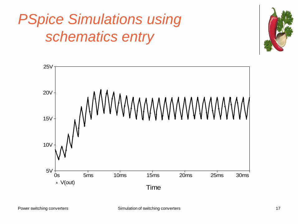
Power switching converters Simulation of switching converters 17
PSpice Simulations using
schematics entry
Time
0s 5ms 10ms 15ms 20ms 25ms 30ms
V(out)
5V
10V
15V
20V
25V

Power switching converters Simulation of switching converters 18
PSpice Simulations using
schematics entry
Time
0s 5ms 10ms 15ms 20ms 25ms 30msI(L
1) I(C
1)
-2.0A
-1.0A
0A
1.0A
2.0A
3.0A
I(C1)
I(L1)

Power switching converters Simulation of switching converters 19
PSpice Simulations Using
Behavioral Modeling
ABM.OLB part library
Control system parts
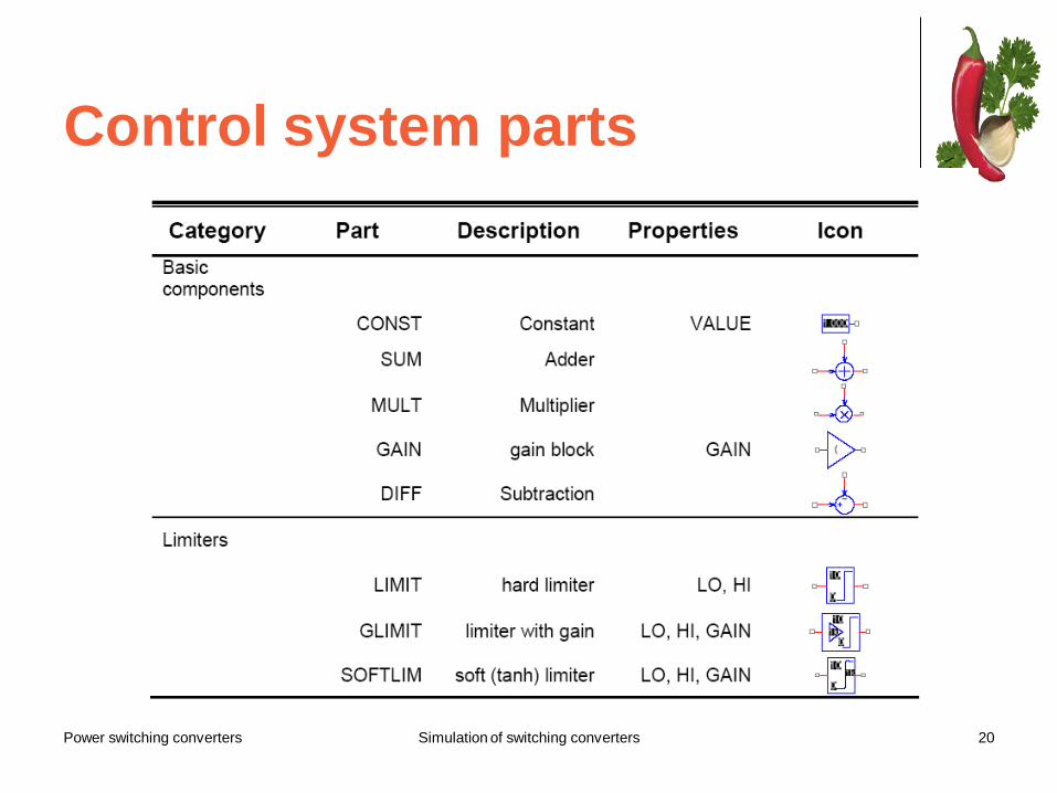
Power switching converters Simulation of switching converters 20
Control system parts

Power switching converters Simulation of switching converters 21
Control system parts
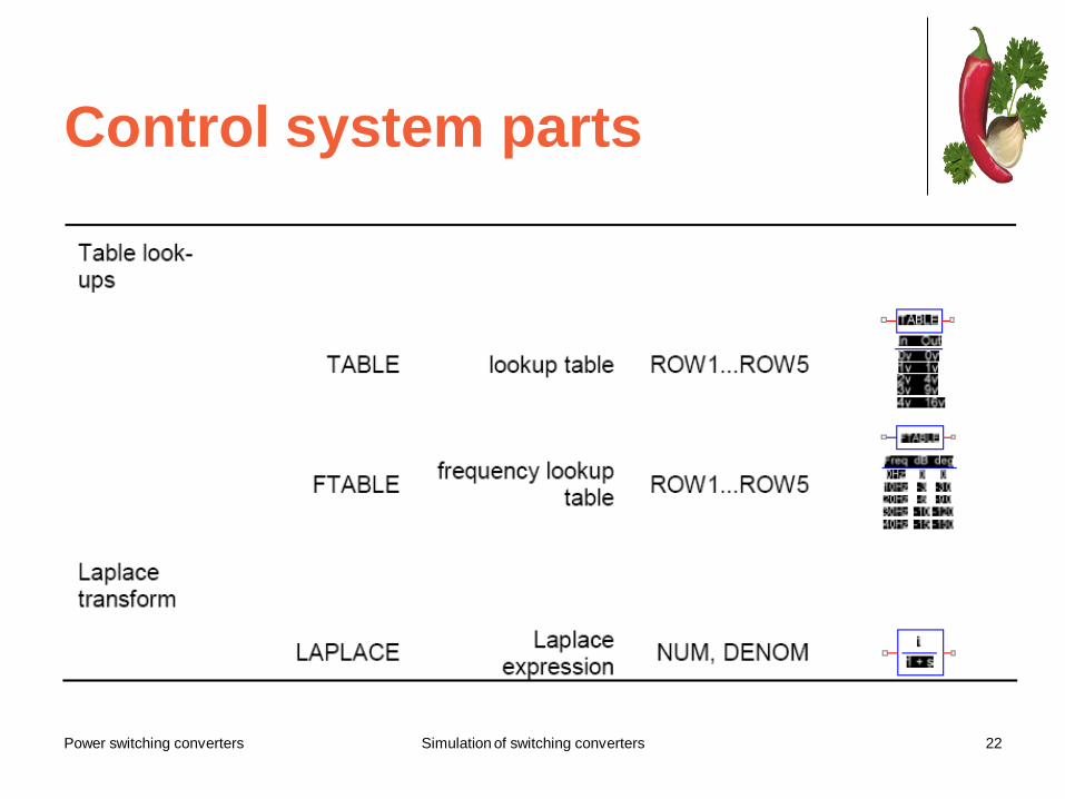
Power switching converters Simulation of switching converters 22
Control system parts

Power switching converters Simulation of switching converters 23
Control system parts

Power switching converters Simulation of switching converters 24
Control system parts

Power switching converters Simulation of switching converters 25
PSpice-equivalent parts

Power switching converters Simulation of switching converters 26
PSpice-equivalent parts

Power switching converters Simulation of switching converters 27
Operators in ABM expressions

Power switching converters Simulation of switching converters 28
Operators in ABM expressions

Power switching converters Simulation of switching converters 29
Functions in arithmetic
expressions

Power switching converters Simulation of switching converters 30
Functions in arithmetic
expressions

Power switching converters Simulation of switching converters 31
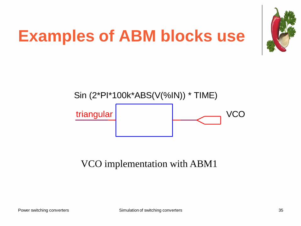
Examples of ABM blocks use
PARAMETERS:
PI = 3.141592654freq = 1k
3*sin (2*PI*freq*TIME)
sine
ABM and PARAM

Power switching converters Simulation of switching converters 32
Examples of ABM blocks use
control
3*V (sine)
Node voltages can be accessed from ABM blocks

Power switching converters Simulation of switching converters 33
Examples of ABM blocks use
rmssine
If (TIME<=0,0,SQRT(SDT(PWR(V(%IN),2))/TIME))
RMS meter
If(argument,then,else)
If (TIME<=0, 0, SQRT(SDT(PWR(V(%IN),2))/TIME))
Power switching converters Simulation of switching converters 34
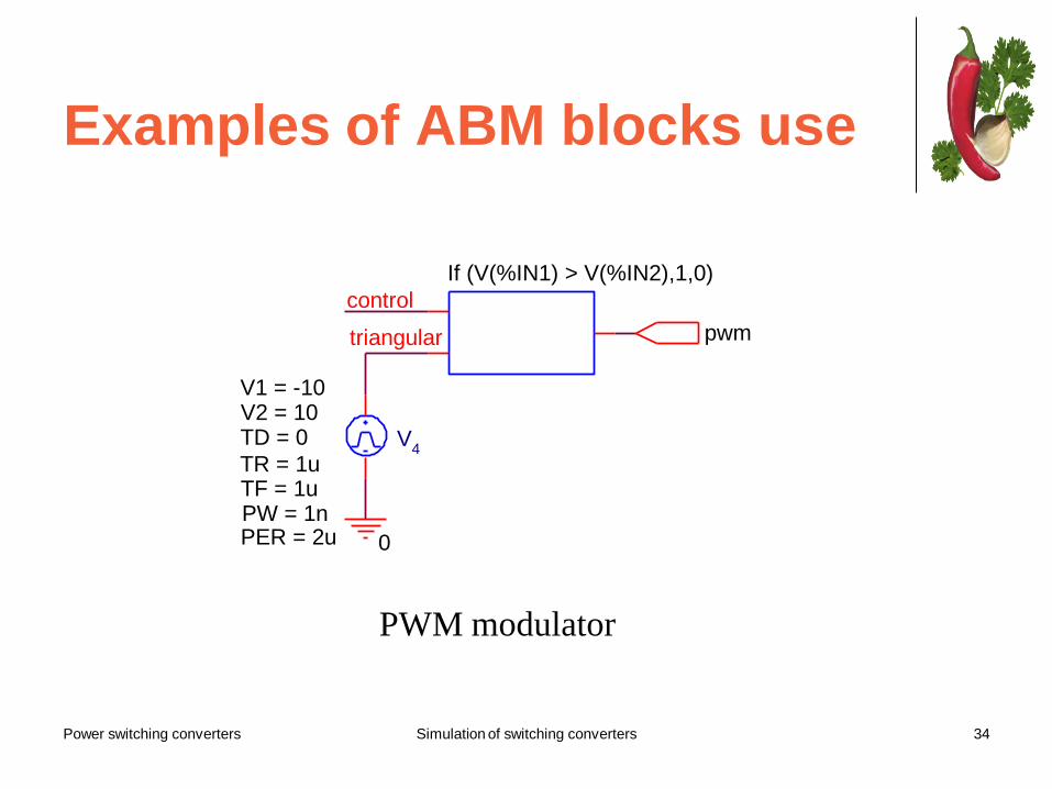
Examples of ABM blocks use
control
pwm
0
If (V(%IN1) > V(%IN2),1,0)
V4
triangular
TD = 0
TF = 1uPW = 1nPER = 2u
V1 = -10
TR = 1u
V2 = 10
PWM modulator
Power switching converters Simulation of switching converters 35
Examples of ABM blocks use
Sin (2*PI*100k*ABS(V(%IN)) * TIME)
VCOtriangular
VCO implementation with ABM1

Power switching converters Simulation of switching converters 36
PSpice Simulations Using Control
Blocks
control
0
pwmtriangular
V4
TD = 0
TF = 0.5mPW = 1nPER = 1m
V1 = -10
TR = 0.5m
V2 = 10
100k10
0
PWM modulator with control blocks

Power switching converters Simulation of switching converters 37
PSpice Simulations Using Control
Blocks
0
OpAmp
V4
1Vac
0Vdc
50
50 + sIN OUT
PARAMETERS:
Vcc
= +12
VEE
= 0
0
0
Vcc
VEE
In-
0
In+
R2
10Meg
100k
R1
10Meg
Model of an operational amplifier

Power switching converters Simulation of switching converters 38
PSpice Simulations Using Control
Blocks
Frequency
10mHz 1.0Hz 100Hz 10KHz 1.0MHz 100MHz1.0mHz
P(V(OPAMP))
-100d
-50d
0dDB(V(OPAMP))
-50
0
50
100
SEL>>
Open loop frequency response

Power switching converters Simulation of switching converters 39
PSpice Simulations Using Control
Blocks
V4
1Vac
0Vdc
R3
10k
OpAmp
0
R2
10Meg
R1
10Meg
0
In-
R4
1k
50
50 + sIN OUT
In+
0
PARAMETERS:
Vcc
= +12
VEE
= 0
100k
Vcc
VEE
0
Closed loop amplifier

Power switching converters Simulation of switching converters 40
PSpice Simulations Using Control
Blocks
Frequency
10mHz 1.0Hz 100Hz 10KHz 1.0MHz 100MHz1.0mHz
P(V(OPAMP))
-100d
-50d
0d
SEL>>
DB(V(OPAMP))-50
0
50
Closed loop frequency response

Power switching converters Simulation of switching converters 41
Voltage –mode PWM boost
converter
Error amplifier
3
C1
0
0
1Meg
1Meg+s
pwm_out
If (V(%IN1) > V (%IN2),1,0)control
5
Dbreak
D1
12
-12V
ref
out
saw
V1
10Vdc
+-
+
-
S1
S VON = 1.0VVOFF = 0.0V
ROFF = 1e6RON = 0.05
error
R2
1
pwm
sense
V4TD = 0
TF = 1nPW = 1nPER = 1m
V1 = 0
TR = 999u
V2 = 10
PWM
modulator
R1
0
L1
10mH
-++-
E1
E
GAIN = 0.25
20100µF
+
-

Power switching converters Simulation of switching converters 42
Voltage –mode PWM boost
converter
Time
0s 1ms 2ms 3ms 4ms 5ms 6ms 7ms 8ms 9ms 10msV(out) AVG (V(out))
0V
20V
40VV(error) AVG (V(error))
-20V
0V
20VV(control) AVG (V(control))
0V
10V
20V
SEL>>
AVG (V(out))
V(out)
V(error)
AVG (V(error))
V(control)
AVG(V(control))

Power switching converters Simulation of switching converters 43
PSpice simulations using vendor
models
TL084
+
-
V+
V-
D1
MUR420
sense
L1
10mHIC = 0
R7
1
0
0
pwm_out
-15
saw
R6
100
+15
Vref
out
+15
R3
100k
R5
3k
R4
1k
V4TD = 0
TF = 1nPW = 1nPER = 1m
V1 = 0
TR = 999u
V2 = 10
pwm
R2
300k
R8
300
PWM modulator
5
control
V1
10Vdc
Error amplifier
C1
100uF
LM311
+
-GV
+V
-
B/S B
R1
20
0
X2
MTP15N05E/MC ESR
10m
-15
+
-
.TRAN 0 30m 0 0.1u
.OPTIONS STEPGMIN
.OPTIONS ABSTOL= 10p
.OPTIONS ITL1= 400
.OPTIONS ITL4= 500
.OPTIONS RELTOL= 0.01
.OPTIONS VNTOL= 10u

Power switching converters Simulation of switching converters 44
PSpice simulations using vendor
models
Time
0s 5ms 10ms 15ms 20ms 25ms 30msV(out)
0V
10V
20V
SEL>>
V(control)4.8V
5.0V
5.2VI(L
1)
0A
2.0A
4.0A

Power switching converters Simulation of switching converters 45
Vorperian models for PSpice
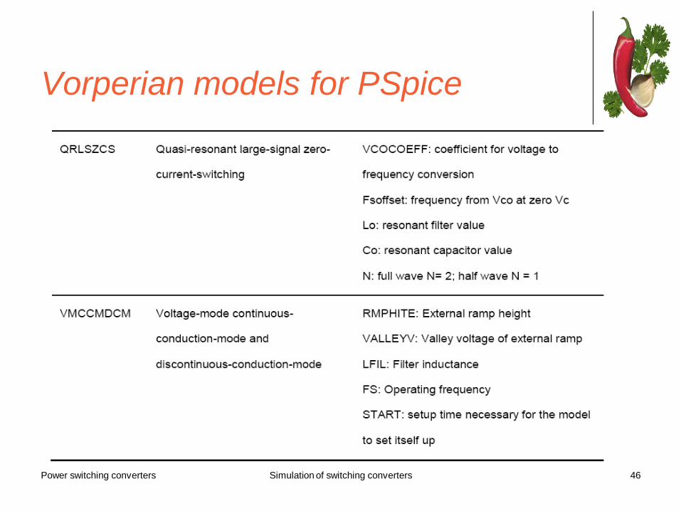
Power switching converters Simulation of switching converters 46
Vorperian models for PSpice

Power switching converters Simulation of switching converters 47
Vorperian models for PSpice

Power switching converters Simulation of switching converters 48
Vorperian models for PSpice **** VMSSCCM ****
* Small signal continuous conduction voltage mode model
* Params: RMPHITE --> External ramp height
* D --> Duty cycle
* Ic --> Current flowing from terminal C
* Vap --> Voltage across terminal A P
* Rsw --> Switch on resistance
* Rd --> diode on resistance
* Rm --> which models the base storage effects
* Re --> models ripple across esr of cap
* Pins control voltage --
* common -------- |
* passive----- | |
* active -- | | |
.subckt VMSSCCM A P C VC Params: RMPHITE=2 D=0.4 IC=1 VAP=20
+ Rsw=1e-6 Rd=1e-6 Re=1e-6 Rm=1e-6
efm 4 0 value =v(Vc)/rmphite
e2 A 6 value=v(0,4)*Vap/d
g1 A P value=v(4)*IC
gxfr 6 P VALUE=I(vms)*D
exfr 9 P VALUE=V(6,P)*D
vms 9 8 0
rd 8 C d*rd+(1-d)*rsw+d*(1-d)*re+rm
rope 4 0 1g
rgnd 0 P 1g
.ends

Power switching converters Simulation of switching converters 49
Small-signal analysis of switching
converters
R20
0
U7
VMSSCCM
D = 0.5IC = -1.84
RD = 1e-6
RE = 10mRM = 1e-6
RMPHITE = 10
RSW = 10mVAP = -17.6
1
3
2
4
A
C
P
VC
Rs1
300k
out
Rs
1
Resr
10m
V1
10Vdc
0
L1
10mHIC = 0
Rs2
100k
sense
V4
1Vac
0Vdc
Cout
100uFIC = 0
+
-
Small-signal AC analysis

Power switching converters Simulation of switching converters 50
Small-signal analysis of switching
converters
Time
0s 5ms 10ms 15ms 20ms 25ms 30msV(OUT)
0V
10V
20V
SEL>>
I(L1)
0A
1.0A
2.0A
3.0A

Power switching converters Simulation of switching converters 51
Small-signal analysis of switching
converters
Frequency
1.0Hz 10Hz 100Hz 1.0KHz 10KHz 100KHz 1.0MHz
P(V(OUT))
-300d
-200d
-100d
-0dDB(V(OUT))
-80
-40
0
40
SEL>>
Open-loop transfer function

Power switching converters Simulation of switching converters 52
Small-signal analysis of switching
converters
U7
VMSSCCM
D = 0.5IC = -1.84
RD = 1e-6
RE = 10mRM = 1e-6
RMPHITE = 10
RSW = 10mVAP = -17.6
1
3
2
4
A
C
P
VC
Rs2
100k
Resr
10m
0V
4
1Vac
10Vdc
L1
10mHIC = 0
Rs
1
R
20 sense
out
Cout
100uFIC = 0
Rs1
300k
0
Input impedance
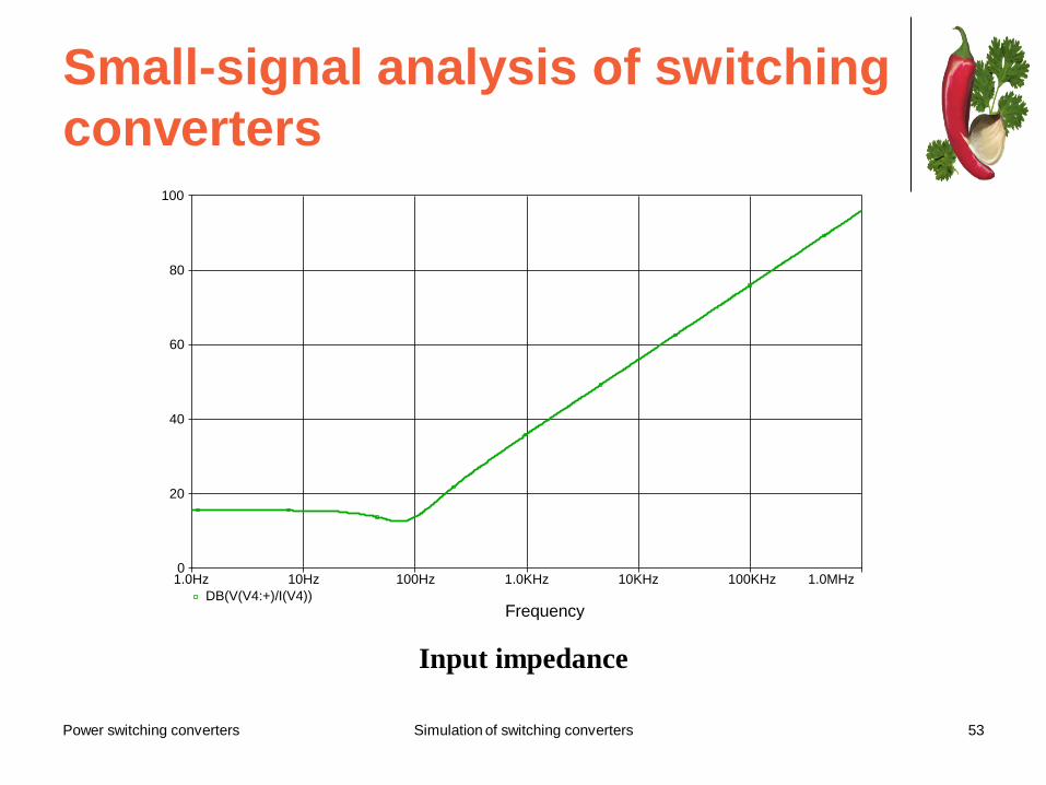
Power switching converters Simulation of switching converters 53
Small-signal analysis of switching
converters
Frequency
1.0Hz 10Hz 100Hz 1.0KHz 10KHz 100KHz 1.0MHz
DB(V(V4:+)/I(V4))
0
20
40
60
80
100
Input impedance

Power switching converters Simulation of switching converters 54
Small-signal analysis of switching
converters
Output impedance
sense0
U7
VMSSCCM
D = 0.5IC = -1.84
RD = 1e-6
RE = 10mRM = 1e-6
RMPHITE = 10
RSW = 10mVAP = -17.6
1
3
2
4
A
C
P
VC
L1
10mHIC = 0
Resr
10m
0
out
Rs2
100k
V4
1Vac
10Vdc
R
20
Rs
1
V5
10Vdc
Rs1
300kC
out
100uFIC = 0
+
-
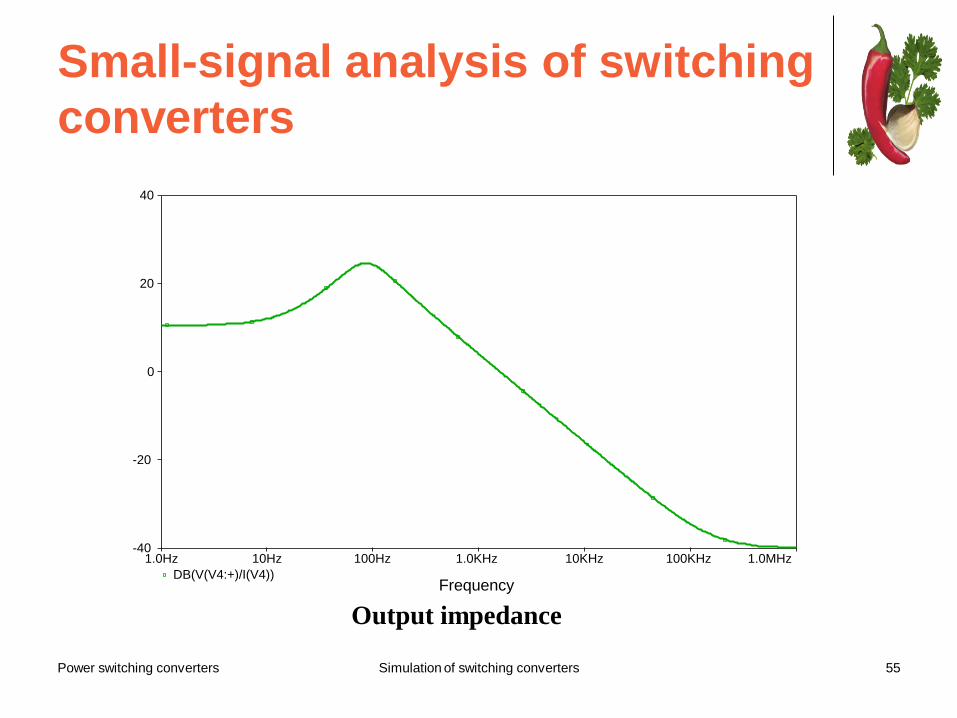
Power switching converters Simulation of switching converters 55
Small-signal analysis of switching
converters
Output impedance
Frequency
1.0Hz 10Hz 100Hz 1.0KHz 10KHz 100KHz 1.0MHz
DB(V(V4:+)/I(V4))
-40
-20
0
20
40

Power switching converters Simulation of switching converters 56
Small-signal analysis of switching
converters
L1
10mHIC = 0
Rs
1
Rs1
300k
U7
VMSSCCM
D = 0.5IC = -1.84
RD = 1e-6
RE = 10mRM = 1e-6
RMPHITE = 10
RSW = 10mVAP = -17.6
1
3
2
4
A
C
P
VC
Rs2
100k
V1
10Vdc
sense
0
0
V4
TD = 20m
TF = 1nPW = 50mPER = 50m
V1 = 1.2
TR = 1n
V2 = 1.5
Cout
100uFIC = 0
Resr
10m
R
20
out
+
-
Small-signal transient analysis

Power switching converters Simulation of switching converters 57
Small-signal analysis of switching
converters
Small-signal transient analysis
Time
0s 5ms 10ms 15ms 20ms 25ms 30ms
I(L1)
0A
1.0A
2.0A
3.0AV(OUT)
0V
10V
20V
25V
SEL>>

Power switching converters Simulation of switching converters 58
Averaged-inductor model for a
voltage-mode boost converter
C1
100uIC = 0
V1
10
R2
20
R1
10m
0.5
out
U7 BOOSTVM
Rs = 1
FS = 1k
L = 10m
DON
IN OUT
GND
R3
1
0
+
-

Power switching converters Simulation of switching converters 59
Output voltage obtained with the
averaged-inductor model
Time
0s 5ms 10ms 15ms 20ms 25ms 30msV(OUT)
0V
5V
10V
15V
20V
25V
30V

Power switching converters Simulation of switching converters 60
Measuring the loop gain
0
V1
1Vac
0Vdc
R
20
0
0
Vf
0
Rs
1
-++-
E1
E
GAIN = 0.25
Vg
10Vdc
Cout
100uFIC = 0
Resr
10m
U7VMSSCCM
D = 0.5IC = -1.84
RD = 1e-6
RE = 10mRM = 1e-6
RMPHITE = 10
RSW = 10mVAP = -17.6
1
3
2
4
A
C
P
VC
L1
10mHIC = 0 out
0
+
-

Power switching converters Simulation of switching converters 61
Measuring the loop gain
Frequency
1.0mHz 10mHz 100mHz 1.0Hz 10Hz 100Hz 1.0KHz 10KHz 100KHz 1.0MHz 10MHzP(V(VF))
-360
-270
-180
-90
0
90
SEL>>
(100.000,-163.029)
DB(V(VF))-80
-40
0
20(100.000,-1.2488)
Power switching converters Simulation of switching converters 62
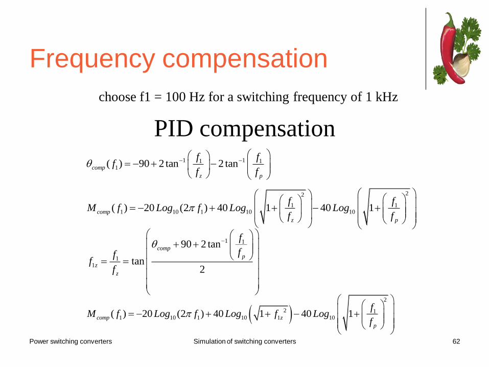
Frequency compensation
choose f1 = 100 Hz for a switching frequency of 1 kHz
PID compensation 1 11 1
1( ) 90 2 tan 2 tancomp
z p
f ff
f f
22
1 11 10 1 10 10( ) 20 (2 ) 40 1 40 1comp
z p
f fM f Log f Log Log
f f
1 1
11
90 2 tan
tan2
comp
p
z
z
f
fff
f
2
2 11 10 1 10 1 10( ) 20 (2 ) 40 1 40 1comp z
p
fM f Log f Log f Log
f

Power switching converters Simulation of switching converters 63
PID compensation
1p
3 3
1 = f
2 CR
2
1 2
p
2 1 2
( + )C C = f
2 C CR
1z
2 1
1 = f
2 CR
2z
1 3 3
1 = f
2 ( + )CR R
21
1
R = K
R
2 1 32
1 3
( + )R R R = K
R R
3 1 23
2 1 2
C CR = .C
+ C CR
Mag_comp_f1 = -7.0985
Ph_comp = 32
k1_db = -24.6094
k1 = 0.0588
k2_db = -5.0259
k2 = 0.5607
R2 = 588.2076
R3 = 269.7258
C1 = 5.0034e-005
C2 = 1.3496e-006
C3 = 2.8658e-006

Power switching converters Simulation of switching converters 64
Boost switching converter with
PID compensator
-15
pwmR
s
1
+15
saw
Cout
100uFIC = 20
L1
10mHIC = 4
C1
5.0014e-005
R2
518.3291
V110V
dc
0
R1
10k
0
-15
sense
R6
100
V3
-15
out
5
+15
LM311
+
-G
V+
V-
B/S B
Rs3
1k
0
0
D1
MUR420
+15
C3
2.5483e-006
Error amplifier
R
20
R4
10meg
Vref
V4TD = 0
TF = 1nPW = 1nPER = 1m
V1 = 0
TR = 999u
V2 = 10
Rs2
3k
TL084
+
-
V+
V-
ESR
10m
R8
300
R3
173.0498
V2`15
control
VX2
MTP15N05E/MC
PWM
modulator
C2
1.1461e-006
-15
pwm_out
+
-

Power switching converters Simulation of switching converters 65
Simulation results with a PID
compensator
Time
0s 5ms 10ms 15ms 20ms 25ms 30msV(out)
0V
20V
40VV(control)
5.0V
7.5V
10.0V
SEL>>
I(L1)
4.0A
4.5A
5.0A

Power switching converters Simulation of switching converters 66
PI compensation
0 Cout
200uFIC = 0
0
EAO
0
10
-10
L1
10mHIC = 0
Vg
10Vdc
Rs
1out
100k
Resr
10m
0
10
10 + s
error
R
20
Vf
0
R1
1k
V1
1Vac
0Vdc
Vf
C1
500n
U7VMSSCCM
D = 0.5IC = -1.84
RD = 1e-6
RE = 10mRM = 1e-6
RMPHITE = 10
RSW = 10mVAP = -17.6
1
3
2
4
A
C
P
VC
0
-++-
E1
E
GAIN = 0.25
R2
10k
+
-
Small-signal model of the boost converter with PI
compensation
1 1
1 2
1sC RTF
sC R

Power switching converters Simulation of switching converters 67
PI compensation
Frequency
1.0mHz 10mHz 100mHz 1.0Hz 10Hz 100Hz 1.0KHz 10KHz 100KHz 1.0MHz
P(V(VF)) P(V(EAO))
-360
-270
-180
-90
0
90
180
DB(V(VF)) DB(V(EAO))-200
-100
0
SEL>>
Compensated loop gain
Uncompensated loop gain
Compensated loop gain
Uncompensated loop gain
100
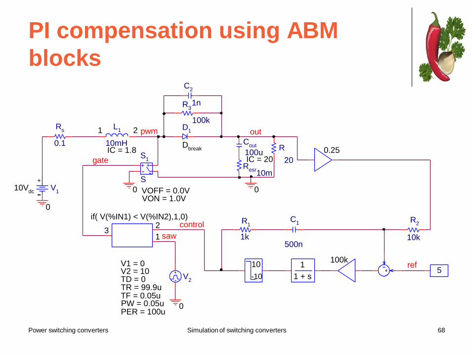
Power switching converters Simulation of switching converters 68
PI compensation using ABM
blocks
0
saw
Resr
10m
0
51
1 + s
out
Dbreak
D1
10
-10
R2
10k
R1
1k
R3
100k
if( V(%IN1) < V(%IN2),1,0)
13
2
V2TD = 0
TF = 0.05uPW = 0.05uPER = 100u
V1 = 0
TR = 99.9u
V2 = 10
C1
500n
C2
1n
+-
+
-
S1
S
VON = 1.0VVOFF = 0.0V
Cout
100uIC = 20
Rs
0.1
ref
0
0
R
20gate
100k
L1
10mHIC = 1.8
1 2
V1
10Vdc
pwm
control
0.25
+
-

Power switching converters Simulation of switching converters 69
Simulation results of the PI
compensation using ABM blocks
Time
0s 5ms 10ms 15ms 20ms 25ms 30msV(CONTROL)
0V
5V
10VV(OUT)
0V
10V
20V
30V
SEL>>
I(L1)
0A
2.0A
4.0A

Power switching converters Simulation of switching converters 70
PI compensation using vendor
models
R3
10
0
R1
1k
-15
+15
V110V
dc
V2
TD = 0
TF = 0.05uPW = 0.05uPER = 100u
V1 = 0
TR = 99.9u
V2 = 10
-15
Cout
100uIC = 20
0
ref
0
0
gate
out
X1
MTP15N05E/MC
R
20
0
Rs
0.1
V3
+15Vdc
C1
500nLM311
+
-G
V+
V-
B/S BR
6
1k
TL084
+
-
V+
V-
5
0
L1
10mHIC = 1.8
1 2
R5
3k
0
R2
10k
saw
-15
Resr
10m
control
+15
pwm
V4
-15Vdc
D2
MUR420
R4
300
+15
+
-
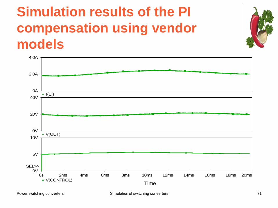
Power switching converters Simulation of switching converters 71
Simulation results of the PI
compensation using vendor
models
Time
0s 2ms 4ms 6ms 8ms 10ms 12ms 14ms 16ms 18ms 20ms
V(CONTROL)
0V
5V
10V
SEL>>
V(OUT)0V
20V
40VI(L
1)
0A
2.0A
4.0A
Power switching converters Simulation of switching converters 72
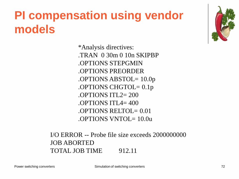
PI compensation using vendor
models
*Analysis directives:
.TRAN 0 30m 0 10n SKIPBP
.OPTIONS STEPGMIN
.OPTIONS PREORDER
.OPTIONS ABSTOL= 10.0p
.OPTIONS CHGTOL= 0.1p
.OPTIONS ITL2= 200
.OPTIONS ITL4= 400
.OPTIONS RELTOL= 0.01
.OPTIONS VNTOL= 10.0u
I/O ERROR -- Probe file size exceeds 2000000000
JOB ABORTED
TOTAL JOB TIME 912.11

Power switching converters Simulation of switching converters 73
Creating capture symbols for PSpice
simulation •Vendors often provide PSpice models for their circuit
components. They are normally provided in a text file with
extension .LIB; if the file has a different extension, it should be
changed to .LIB
•Start the PSpice Model Editor and from the File menu, choose
Create Parts
•Browse to find the input model library (.LIB file) and click
OK to start
•This step creates an .OBL file with a schematic symbol linked
to your model
•To place the new part into the schematic, open Capture, and
from the Place menu choose Part. Click Add library, then find
and add the new “.OLB” file
Power switching converters Simulation of switching converters 74
Solving convergence
problems
PSpice uses the Newton-Raphson algorithm to solve the nonlinear equations in these analyses
The algorithm is guaranteed to converge only if the analysis is started close to the solution
If the initial guess is far away from the solution, this may cause a convergence failure or even a false convergence
If the node voltages do not settle down within a certain number of iterations, an error message will be issued

Power switching converters Simulation of switching converters 75
DC analysis error messages
The DC Analysis calculates the small-signal bias points before starting the AC analysis or the initial transient solution for the transient analysis
Solutions to the DC analysis may fail to converge because of incorrect initial voltage guesses, model discontinuities, unstable or bistable operation, or unrealistic circuit impedances
When an error is found during the DC analysis, SPICE will then terminate the run because both the AC and transient analyses require an initial stable operating point in order to start

Power switching converters Simulation of switching converters 76
DC analysis error messages
No convergence in DC analysis
PIVTOL Error
Singular Matrix
Gmin/Source Stepping Failed
No Convergence in DC analysis at Step = xxx

Power switching converters Simulation of switching converters 77
Transient analysis error messages
If the node voltages do not settle down, the time step is reduced and SPICE tries again to determine the node voltages
If the time step is reduced beyond a certain fraction of the total analysis time, the transient analysis will issue an error message “Time step too small” and the analysis will be halted
Transient analysis failures are usually due to model discontinuities or unrealistic circuit, source, or parasitic modeling

Power switching converters Simulation of switching converters 78
Solutions to convergence
problems
There are two ways to solve convergence problems
the first only tries to fix the symptoms by adjusting the simulator options
while the other attacks the root cause of the convergence problems
Once the circuit is properly modeled, many of the modifications of the "options" parameters will no longer be required
It should be noted that solutions involving simulation options may simply mask the underlying circuit instabilities

Power switching converters Simulation of switching converters 79
Bias point (DC) convergence
Checking circuit topology and connectivity
Modeling of circuit components
PSpice options are checked to ensure that
they are properly defined

Power switching converters Simulation of switching converters 80
Checking circuit topology and
connectivity
Make sure that all of the circuit connections are valid
Check for incorrect node numbering or dangling nodes
Verify component polarity
Check for syntax mistakes
Make sure that the correct PSpice units (i.e. MEG for 1E6, not M, which means mili in simulations) are used

Power switching converters Simulation of switching converters 81
Make sure that there is a DC path from every node to ground
Make sure that there are at least two connections at every node
Make sure that capacitors and/or current sources are not connected in series
Make sure that no (groups of) nodes are isolated from ground by current sources and/or capacitors
Make sure that there are no loops of inductors and/or voltage sources only

Power switching converters Simulation of switching converters 82
Place the ground (node 0) somewhere in the
circuit
Be careful when floating grounds (e.g., chassis
ground) are used; a large resistor should be
connected from the floating node to ground. All
nodes will be reported as floating if "0 ground" is
not used
Make sure that voltage/current generators use
realistic values, and verify that the syntax is
correct
Make sure that dependent source gains are
correct, and that E/G element expressions are
reasonable

Power switching converters Simulation of switching converters 83
Verify that division by zero or LOG(0) cannot occur
Voltages and currents in PSpice are limited to the range +/- 1e10
Avoid using digital components, unless really necessary
Initialize the digital nodes with valid digital values
Avoid situations where an ideal current source delivers current into a reverse-biased p-n junction without a shunt resistance

Power switching converters Simulation of switching converters 84
Setting up the options for the
analog simulation
Increase ITL1 to 400
Use NODESETs to set node voltages to the nearest reasonable guess at their DC values
Enable the GMIN stepping algorithm
Set PREORDER in Simulation Profiles options
Setting the value of ABSTOL to 1 µ
PSpice does not always converge when relaxed tolerances are used
Setting GMIN to a value between 1n and 10n will often solve convergence problems
Setting GMIN to a value, which is greater than 10n, may cause convergence problems

Power switching converters Simulation of switching converters 85
Transient convergence
The transient analysis can fail to complete if
the time step becomes too small
This can be due to either
(a) the Newton-Raphson iterations would not
converge even for the smallest time step size
(b) something in the circuit is moving faster than
can be accommodated by the minimum step size

Power switching converters Simulation of switching converters 86
Transient convergence
The circuit topology and connectivity should
first be checked
Followed by the PSpice options

Power switching converters Simulation of switching converters 87
Circuit topology and
connectivity
Avoid using digital components, unless really
necessary
Initialize the nodes with valid digital value to ensure
there are no ambiguous states
Use RC snubbers around diodes
Add Capacitance for all semiconductor junctions

Power switching converters Simulation of switching converters 88
Circuit topology and
connectivity Add realistic circuit and element parasitics
It is important that switching times be nonzero
It is recommended that all inductors have a parallel resistor
Look for waveforms that transition vertically (up or down) at the point during which the analysis halts

Power switching converters Simulation of switching converters 89
Circuit topology and
connectivity
Increase the rise/fall times of the PULSE
sources
Ensure that there is no unreasonably large
capacitor or inductor

Power switching converters Simulation of switching converters 90
PSpice options
Set RELTOL=.01
Reduce the accuracy of ABSTOL/VNTOL if
current/voltage levels allow it
ABSTOL and VNTOL should be set to about 8
orders of magnitude below the level of the maximum
voltage and current
Increase ITL4, but no more than 100

Power switching converters Simulation of switching converters 91
PSpice options
Skipping the bias point is not recommended
Any applicable .IC and IC= initial conditions
statements should be added to assist in the
initial stages of the transient analysis

Power switching converters Simulation of switching converters 92
Switching converter simulation using
Matlab Working with transfer functions
Consider a buck converter designed to operate in the continuous conduction
mode having the following parameters: R = 4Ω, L = 1.330 mH, C = 94 µf, Vs =
42 V, Va = 12 V
1 2
2
2
0 0
1 1( )
( )1
o z z
d
s s
s sv sK
s sd s
Q
2(1 )
sd
VK
D
1
1z
ESR
sR C
2
2
(1 )( || ) ind
z ESR
RDs R R R
L L
0
(1 )1 ind e
ESR
R r D D
R RLC
||e ESRr R R
0
(1 ) 1
( )ind e
ESR
QR r D
L C R R

Power switching converters Simulation of switching converters 93
Switching converter simulation using
Matlab % this is a comment
% parameters
R= 4;
L = 1.330 e-3;
Rind = 100 e-3;
C = 94 e-6;
Resr = 10 e-3
Vs = 42;
Va = 12;
D=Va/Vs;
Kd= Vs/(1-D)^2;
Sz1=1/(Resr*C);
Req = R-(Resr*R/(Resr+R));
Sz2 = (1/L)*(1-D)^2* Req – Rind/L;
Re=(Resr*R)/( Resr+R);
Wo = (1/sqrt(L*C)) * sqrt((Rind+re*D*(1-D))/(Resr+R));
Q = Wo/(((Rind+re*(1-D))/L)+(1/(C*(Resr+R))));

Power switching converters Simulation of switching converters 94
Switching converter simulation using
Matlab % polynomials are entered in descending order of S.
n1=[1/Sz1 1]
n2=[-1/Sz2 1]
NUM=conv(n1,n2)
% the convolution realizes the product of 2 polynomials
% define denumerator
DEN = [1/(Wo^2) 1/(Wo*Q) 1]
% create TF variable
sysTF = Kd * tf(NUM,DEN)
which returns
Transfer function:
-5.317e-008 s^2 - 0.05648 s + 82.32
4.913e-006 s^2 + 0.01343 s + 1sysTF
Power switching converters Simulation of switching converters 95
Switching converter simulation using
Matlab
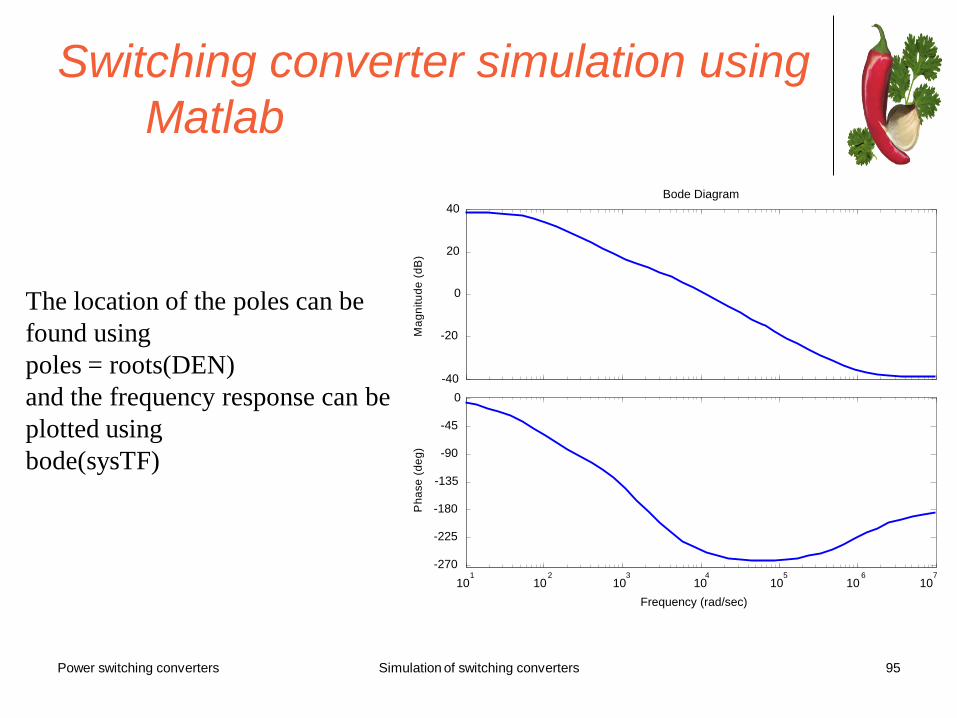
The location of the poles can be
found using
poles = roots(DEN)
and the frequency response can be
plotted using
bode(sysTF)
Bode Diagram
Frequency (rad/sec)
Ph
ase
(de
g)
Ma
gn
itu
de
(dB
)
-40
-20
0
20
40
101
102
103
104
105
106
107
-270
-225
-180
-135
-90
-45
0

Power switching converters Simulation of switching converters 96
Switching converter simulation using
Matlab The small signal transient step response can be plotted using
Figure % this command opens a new figure window
step(sysTF) Step Response
Time (sec)
Am
plitu
de
0 0.01 0.02 0.03 0.04 0.05 0.06 0.07 0.08-10
0
10
20
30
40
50
60
70
80
90

Power switching converters Simulation of switching converters 97
Switching converter simulation using
Matlab
Working with matrices
Consider a buck converter designed to operate in the continuous conduction mode
having the following parameters: R = 4Ω, L = 1.330 mH, C = 94 µf, Vs = 42 V, Va
= 12 V.
% state-space averaged model of a Buck converter
Rload= 4; % load resistance
L= 1.330e-3; % inductance
cap=94.e-6; % capacitance
Ts=1.e-4; % switching period
Vs=42; % input DC voltage
Vref=12; % desired output voltage
The average duty cycle is:
D=Vref/(Vs); % ideal duty cycle

Power switching converters Simulation of switching converters 98
Switching converter simulation using
Matlab ^
^ ^ ^1
^
2
10
1 10 0
sVDxL
x u dL L
xC RC
A=[ 0 -1/L
1/cap -1/(Rload*cap)]
B1=[ 1/L
0]; %during Ton
B2=[ 0
0]; %during Toff
B=B1*D+B2*(1-D)
C=[0 1];

Power switching converters Simulation of switching converters 99
Switching converter simulation using
Matlab
OLpoles = eig(A)
sysOL=ss(A,B,C,0)
step(sysOL)
Time (sec.)
Am
plitu
de
Step Response
0 0.5 1 1.5 2 2.5 3 3.5 4 4.5
x 10-3
0
0.05
0.1
0.15
0.2
0.25
0.3
0.35
From: U (1)
To
:Y
(1)

Power switching converters Simulation of switching converters 100
Switching converter simulation using
Matlab
gamma=[ Vs/L
0];
closed-loop poles:
P=1e3*[-0.3298 + 0.10i -0.3298 - 0.10i]';
Bf= gamma*(D/Vref);
F=place(A,Bf ,P)

Power switching converters Simulation of switching converters 101
Switching converter simulation using
Simulink
-5.317e-8 s^2 - 0.05648 s + 82.32
4.913e-6 s^2 + 0.01343 s + 1sysTF
[NUM,DEN] = TFDATA(sysTF,’v’)
-5.317e-8s -0.0565s+82.322
4.913e-6s +0.0134s+1.02
Transfer Fcn
time
To Workspace1
output
To Workspace
Step Scope
Clock
0 0.005 0.01 0.015 0.02 0.025 0.03 0.035 0.04 0.045 0.05-10
0
10
20
30
40
50
60
70
80
90
Time (s)
Ou
tpu
t

Power switching converters Simulation of switching converters 102
Switching converter simulation using
Simulink
sysZPK = zpk(sysTF)
-0.010821 (s+1.064e006) (s-1455)
(s+2657) (s+76.6)sysZPK
zeroes: [-1.0638e+006 +1455]
poles: [-2657 -76.6]
gain: [-0.010821]
-0.010821(s+1.0638e+006)(s-1455)
(s+2657)(s+76.6)
Zero-Pole
time
To Workspace1
output
To Workspace
Step Scope
Clock

Power switching converters Simulation of switching converters 103
Switching converter simulation using
Simulink
0 752
10638 2660
214.82 0 '
0 1 '
0
A
B
C
D
time
To Workspace1
output
To Workspace
Step
x' = Ax+Bu
y = Cx+Du
State-Space
Scope
Clock