simatic s5 1p 243 - siemens · siemens warning risks involved in the use of...
TRANSCRIPT

SIEMENS
SIMATIC S5
1P 243AnalogModulewith FB 160/
FB 161
Equipment Manual
Order No: 6ES5998–0KF21
Subject to change without notice
@ Siemens AG 1989, All rights reserved
Application and Application Area 1
Mechanical Construction 2
Function Description 3
Interrupt Processing 4
Putting into Operation 5
Technical Specifications 6
Programming Instructions 7
8
9
10

@ Copyright Siemens AG 1989 All Rights Reserved
Passing on and reproduction of these documents, or utilization and disclosure of their con-tents is prohibited unless specifically authorized. Violations are cause for damageliability.All rights reserved, particularly in the event a patent is issued or a utility–model patent regis-tered.

SIEMENS
Warning
Risks involved in the use of so-called SIMATIC–compatible modules of non-Siemensma-nufacture
“The manufacturer of a product (SIMATIC in this case) is under the general obligation to givewarning of possible risks attached to his product. This obligation has been extended in recentcourt rulings to include parts supplied by other vendors. Accordingly, the manufacturer is obligedto observe and recognize such hazards as may arise when a product is combined with productsof other manufacture.
For this reason, we feel obliged to warn our customers who use SIMATIC products not toinstall so-called SIMATIC–compatible modules of other manufacture in the form of re-placement or add–on modules in SIMATIC systems.
Our products undergo a strict quality assurance procedure. We have no knowledge as to wheth-er outside manufacturers of so–called SIMATIC–compatible modules have any quality assur-ance at all or one that is nearly equivalent to ours. These so–called SIMATIC– compatible mod-ules are not marketed in agreement with Siemens; we have never recommended the use of so–called SIMATIC– compatible modules of other manufacture. The advertising of these other man-ufacturers for so–called SIMATIC–compatible modules wrongly creates the impression that thesubject advertised in periodicals, catalogues or at exhibitions had been agreed to by us. Whereso–called SIMATIC– compatible modules of non–Siemens manufacture are combined with ourSIMATIC automation systems, we have a case of our product being used contrary to recommen-dations. Because of the variety of applications of our SIMATIC automation systems and the largenumber of these products marketed worldwide, we cannot give a concrete description specifical-ly analyzing the hazards created by these so–called SIMATIC– compatible modules. It is beyondthe manufacturer’s capabilities to have all these so–called SIMATIC–compatible moduleschecked for their effect on our SIMATIC products. If the use of so–called SIMATIC– compatiblemodules leads to defects in a SIMATIC automation system, no warranty for such systems will begiven by Siemens.
In the event of product liability damages due to the use of so–called SIMATIC–compatible mod-ules, Siemens is not liable since we took timely action in warning users of the potential hazardsinvolved in so–called SIMATIC– compatible modules. ”
@) Siernem AG 1990, All rights rexwed

R02192 Contenta
1
22.12.22.32.42.5
33.13.23.33.3.13.3.23.3.33.3.43.43.4.13.4.23.4.2.13.4.2.23.4.2.33.4.3.3.4.3.13.4.3.23.4.3.33.4.43.4.4.13.4.4.23.53.5.1.3.5.23,5.33.63.6.13.6.2.3.6.33.6.43.6.4.13.6.4.23.6.4.33.6.4.43.73.7.13.7.23.7.3
Application and Application Area . . . . . . . . . . . . . . . . . . . . . . . . . . . . . . . . . . . . . 1 – 1
Mechanical Construction . . . . . . . . . . . . . . . . . . . . . . . . . . . . . . . . . . . . . . . . . . . . .2 – 1Dimensions and Mechanical Data. . . . . . . . . . . . . . . . . . . . . . . . . . . . . . . . . . . . . . . 2 – 1Overview of thelndividual Variants . . . . . . . . . . . . . . . . . . . . . . . . . . . . . . . . . . . . . . 2–1Block Diagram 1P 243 – IAA, Full Configuration . . . . . . . . . . . . . . . . . . . . . . . . . 2 – 3Block Diagram 1P 243 – IAB, Partial Configuration . . . . . . . . . . . . . . . . . . . . . . . 2 – 4Block Diagram 1P 243 – IAC, Partial Configuration . . . . . . . . . . . . . . . . . . . . . . . 2 – 5
Function Description . . . . . . . . . . . . . . . . . . . . . . . . . . . . . . . . . . . . . . . . . . . . . . . . . 3 – 1Binary Input . . . . . . . . . . . . . . . . . . . . . . . . . . . . . . . . . . . . . . . . . . . . . . . . . . . . . . . . . . 3 – 1Binary Output . . . . . . . . . . . . . . . . . . . . . . . . . . . . . . . . . . . . . . . . . . . . . . . . . . . . . . . . 3–2Analog Input . . . . . . . . . . . . . . . . . . . . . . . . . . . . . . . . . . . . . . . . . . . . . . . . . . . . . . . . . 3–3Rated Input Ranges . . . . . . . . . . . . . . . . . . . . . . . . . . . . . . . . . . . . . . . . . . . . . . . . . . . 3–3Conversion of the Analog input Signals . . . . . . . . . . . . . . . . . . . . . . . . . . . . . . . . . . 3–4InputCircuitry . . . . . . . . . . . . . . . . . . . . . . . . . . . . . . . . . . . . . . . . . . . . . . . . . . . . . . . . 3–5Digital Representation ofMeasuring Values . . . . . . . . . . . . . . . . . . . . . . . . . . . . . . 3–5Analog Output . . . . . . . . . . . . . . . . . . . . . . . . . . . . . . . . . . . . . . . . . . . . . . . . . . . . . . . . 3–7Jumpering ofAnalog Output . . . . . . . . . . . . . . . . . . . . . . . . . . . . . . . . . . . . . . . . . . . 3–7Digitai/Analog Convertersl and2 . . . . . . . . . . . . . . . . . . . . . . . . . . . . . . . . . . . . . . 3–7Rated Output Range and Resolution . . . . . . . . . . . . . . . . . . . . . . . . . . . . . . . . . . . . 3–7Writing theAnalog Outputs . . . . . . . . . . . . . . . . . . . . . . . . . . . . . . . . . . . . . . . . . . . . 3–7Digital Representation ofAnalog Values . . . . . . . . . . . . . . . . . . . . . . . . . . . . . . . . . 3–8Digital/Analog Converter3 . . . . . . . . . . . . . . . . . . . . . . . . . . . . . . . . . . . . . . . . . . . . . 3–9Rated OutputRangeand Resolution . . . . . . . . . . . . . . . . . . . . . . . . . . . . . . . . . . . . 3 – 9WritingtheAnalog Output . . . . . . . . . . . . . . . . . . . . . . . . . . . . . . . . . . . . . . . . . . . . . 3–9Digital Representation ofAnalog Values . . . . . . . . . . . . . . . . . . . . . . . . . . . . . . . . . 3–9Analog OutputAmplifier . . . . . . . . . . . . . . . . . . . . . . . . . . . . . . . . . . . . . . . . . . . . . . . 3–10Description . . . . . . . . . . . . . . . . . . . . . . . . . . . . . . . . . . . . . . . . . . . . . . . . . . . . . . . . . . 3–10Circuihy . . . . . . . . . . . . . . . . . . . . . . . . . . . . . . . . . . . . . . . . . . . . . . . . . . . . . . . . . . . . . 3–10Analog Value Conditioning Circuit . . . . . . . . . . . . . . . . . . . . . . . . . . . . . . . . . . . . . . 3–11Operating Elements . . . . . . . . . . . . . . . . . . . . . . . . . . . . . . . . . . . . . . . . . . . . . . . . . . . 3–11Functioning . . . . . . . . . . . . . . . . . . . . . . . . . . . . . . . . . . . . . . . . . . . . . . . . . . . . . . . . . . 3–11InputCircuitry . . . . . . . . . . . . . . . . . . . . . . . . . . . . . . . . . . . . . . . . . . . . . . . . . . . . . . . . 3–13Comparatorsand Gating Logic . . . . . . . . . . . . . . . . . . . . . . . . . . . . . . . . . . . . . . . . . 3–14input Signal Range and PossibleCircuitry . . . . . . . . . . . . . . . . . . . . . . . . . . . . . . . 3–14InputCircuitry . . . . . . . . . . . . . . . . . . . . . . . . . . . . . . . . . . . . . . . . . . . . . . . . . . . . . . . . 3–15Reading the Comparatorsand the Gating Logic . . . . . . . . . . . . . . . . . . . . . . . . . . 3–15Evaluation ofthe Comparator States . . . . . . . . . . . . . . . . . . . . . . . . . . . . . . . . . . . . 3–16Representation ofComparator States . . . . . . . . . . . . . . . . . . . . . . . . . . . . . . . . . . . 3–16ValueTableforComparators land2 . . . . . . . . . . . . . . . . . . . . . . . . . . . . . . . . . . . . 3–17Explanation oftheValueTable and the lndividualValues . . . . . . . . . . . . . . . . . . . 3–18Representation intheTime/Voltage Diagram . . . . . . . . . . . . . . . . . . . . . . . . . . . . . 3–19DifferenceAmplifier(P Controller) . . . . . . . . . . . . . . . . . . . . . . . . . . . . . . . . . . . . . . . 3–20input Signal Range andAmplification . . . . . . . . . . . . . . . . . . . . . . . . . . . . . . . . . . . 3–20InputCircuitry . . . . . . . . . . . . . . . . . . . . . . . . . . . . . . . . . . . . . . . . . . . . . . . . . . . . . . . . 3–20Circuitry Possibilities and Output Signal Range . . . . . . . . . . . . . . . . . . . . . . . . . . . 3–20
lP243 Equipment Manual o – [email protected] 1989, ClrderNo:6ES5 gg8-0KF21

Contenta R02192
44.14.24.34.3.14.3,24.44.4,14.4.24.4,3
55.15.25.35.45.55.5.15.5.25.65.75.8
66.1
77.17.27.37.47.5
Interrupt Processing . . . . . . . . . . . . . . . . . . . . . . . . . . . . . . . . . . . . . . . . . . . . . . . . .General Conditions for Interrupt Processing . . . . . . . . . . . . . . . . . . . . . . . . . . . . . .Possibilities for Interrupt Processing . . . . . . . . . . . . . . . . . . . . . . . . . . . . . . . . . . . . .DirectBusAccess . . . . . . . . . . . . . . . . . . . . . . . . . . . . . . . . . . . . . . . . . . . . . . . . . . . .lnterruptProcessing intheS5–1 15U/H . . . . . . . . . . . . . . . . . . . . . . . . . . . . . . . . . .lnterruptProcessing intheS5–135U with CPU 9220rCPU 928A/B . . . . . . . . .Separate interrupt lnputModule . . . . . . . . . . . . . . . . . . . . . . . . . . . . . . . . . . . . . . . .InterruptProcessing inthe S5–135U . . . . . . . . . . . . . . . . . . . . . . . . . . . . . . . . . . . .lnterruptProcessing inthe S5-150U/S . . . . . . . . . . . . . . . . . . . . . . . . . . . . . . . . . .InterruptProcessing inthe S5–155U/H . . . . . . . . . . . . . . . . . . . . . . . . . . . . . . . . . .
4 – 14 – 14 – 14 – 14 – 24 – 6
4 – 1 24 – 1 24 – 1 64 – 2 1
Putting into Operation . . . . . . . . . . . . . . . . . . . . . . . . . . . . . . . . . . . . . . . . . . . . . . . .5 – 1BasicConnector . . . . . . . . . . . . . . . . . . . . . . . . . . . . . . . . . . . . . . . . . . . . . . . . . . . . . . 5–1Front Plate and FrontConnector . . . . . . . . . . . . . . . . . . . . . . . . . . . . . . . . . . . . . . . . 5–1Explanation ofthe Signal Names andAbbreviations . . . . . . . . . . . . . . . . . . . . . . . 5–3LayoutofSetting Elementsand Jumpers . . . . . . . . . . . . . . . . . . . . . . . . . . . . . . . . 5–4Jumpering oftheAnaIog Signals . . . . . . . . . . . . . . . . . . . . . . . . . . . . . . . . . . . . . . . 5–5CircuitryoftheAnalog SignalJumpering . . . . . . . . . . . . . . . . . . . . . . . . . . . . . . . . 5–5Soldering Base PinAssignment . . . . . . . . . . . . . . . . . . . . . . . . . . . . . . . . . . . . . . . . 5–6Jumpering ofthe BinarySignaIs . . . . . . . . . . . . . . . . . . . . . . . . . . . . . . . . . . . . . . . . 5–8lnterruptJumpering . . . . . . . . . . . . . . . . . . . . . . . . . . . . . . . . . . . . . . . . . . . . . . . . . . . 5 – 9Setting the ModuleAddress . . . . . . . . . . . . . . . . . . . . . . . . . . . . . . . . . . . . . . . . . . . . 5–11
Technical Specifications . . . . . . . . . . . . . . . . . . . . . . . . . . . . . . . . . . . . . . . . . . . . .6 – 1lnWhich Slots CanthelP243 Analog Module BeUsed? . . . . . . . . . . . . . . . . . . 6–6
Programming Instructions . . . . . . . . . . . . . . . . . . . . . . . . . . . . . . . . . . . . . . . . . . . . 7 – 1Overview . . . . . . . . . . . . . . . . . . . . . . . . . . . . . . . . . . . . . . . . . . . . . . . . . . . . . . . . . . . . 7–1Function Block FB160(PER:ANL) . . . . . . . . . . . . . . . . . . . . . . . . . . . . . . . . . . . . . . 7–2Function Block FB161 (PER:ANS) . . . . . . . . . . . . . . . . . . . . . . . . . . . . . . . . . . . . . . 7–7Example .....,.. . . . . . . . . . . . . . . . . . . . . . . . . . . . . . . . . . . . . . . . . . . . . . . . . . . . . . 7–12ProgrammingwithoutFB . . . . . . . . . . . . . . . . . . . . . . . . . . . . . . . . . . . . . . . . . . . . . . 7–19
O– i i lP243 Equipment [email protected] 1989j0rderNo: 6ES5998-0KF21

R 02/92 Contents
Texts in these boxes contain important information/instructions which must abso-lutely be observed/followed to ensure correct function or protection of the module.
For clarity’s sake, this equipment manual does not contain complete, detailed information andcannot cover every conceivable operating situation.
Contact your local Siemens office if you require additional information or if a special problem ari-ses which is not covered in sufficient detail by this equipment manual.
In addition, be aware that the contents of this documentation do not constitute a part of a previousor existing agreement, promise, or a legal relationship, and are not intended to alter same.
All obligations on the part of Siemens are based on the respective purchase order which also con-tains the complete and solely valid warranty provisions. This 1P 243 equipment manual neitherwidens nor restricts these contractual warranties.
1P 243 Equipment Manual@ Siemens AG 1989, Order No: 6ES5 998-0KF21
o – Ill

R 02/92 Application and Application Area
1
The 1P 243 is a module for input and output, for preliminary processing, and forjumpering of ana-log signals within short processing times. The submodule in its full configuration has eight quickanalog input channels with max. 35 psec. conversion time, four input channels with analog valueconditioning and four analog output channels. Two comparators allow the comparison of analogvalues with each other and via two value difference amplifiers, the signals can be amplified up to20 times their original strength. All analog signals can be freely jumpered via soldering bases onthe circuit board. This means that as a user you can decide about the individual combinations ofthe available hardware components.
Furthermore, eight digital inputs and eight outputs with direct bus access are available. Custom-er–specific interrupt processing can be effected by means of the jumpering base.
The 1P 243 submodule can be used for the following programmable controllers:
– S5–115U/H– S5–135U– s5–150s/u– S5–155U/H
or expansion units (see section 6.1).
For the programmable S5–115U, an adapter casing is required. No fan assembly is required.
1P 243 Equipment Manual
@ Siemens AG 1989, Order No: 6ES5 998-0KF21
1 – 1
R02192 Mechanical Construction
2 Mechanical Construction2.1 Dimensions and Mechanical Data
The 1P 243 is a printed circuit board in double European format, with dimensions of 233.4 mm x160 mm (DIN 41494). In accordance with the SIMATIC S5 compact peripheral system, the PCBtakes up one slot in the rack. It has a width of 1–1/3 SPS1 (20 mm). 42 Faston connector pins (2.4mm x 0.8 mm) are located on the front plate. The bus connection is made via a second row,48–way base connector. The base connector is located on the upper half. Ground (Mext) connec-tion is provided via contact strips in the guide rails.
Overview of the Individual Variants
The 1P 243 is available in one full–configuration version and two different part-configuration ver-sions. The full–configuration module has the following independent functions:
– 1 Analog/digital converter, 8 channels, 12 bits, 35 psec. conversion time,bipolar or unipolar
– 2 Digital/analog converters, 12 bits, bipolar
– 1 Digital/analog converter, 8 bits, unipolar
– 1 Analog output amplifier
– 4 Analog value conditioning circuits with operating point and amplifier setting
– 2 Difference amplifiers (P controllers) with adjustable gain
– 2 comparators with gating logic connected in series, can be read in statically and/orwith inter-rupt generation (interrupt evaluation is only possible for the SIMATIC S5–150U/S andS5–155U with externally-wired digital input module for interrupt generation).
– 8 binary inputs can be read in statically and/orwith interrupt generation (interrupt evaluation isonly possible for the SIMATIC S5– 150U/S and S5–155U with externally–wired digital inputmodule for interrupt generation).
– 8 binary outputs, 24 V, 200 mA, switching to P potential, not current–limited.
The inputs and outputs of the analog function groups are routed to the analog signal jumperblock. This makes it possible to combine the individual functions to suit user requirements. Allsignals are nonfloating.
1 s~ndard plug–in station
1P 243 Equipment Manual
@ %311WIIS AG 1989, Order No: 6ES5 998-0KF21
2 – 1

Mechanical Construction R 02/92
The following table shows which components are for the part-configuration versions:
Full Con figura- Part Configura- Part Configura-tion Module tion Module tion Module
Type 243- IAA 243-IAB 243–1 AC
ND converter, 12 bits 1 1 —D/A converter, 12 bits 2 — 2D/A converter, 8 bits 1 — 1(with driver)Analog value conditioning circuit 4 4 2Difference amplifier (P controller) 2 — 2Comparators (alarm generation) 2 — —Binaty inputs 8 — —
Binaty outputs 8 — —Interrupt/alarm x — —
2 – 2 1P 243 Equipment Manual@SiemensA(31989, Order No: 6ES5998-0KF21

R 02/92 Mechanical Construction
2.3 Block Diagram 1P 243 – IAA, Full Configuration
tiEzizl8binaryinputs
. .
1P 243 Equipment Manual@ Siemens AG 1989, order No: 6ES5 998-0KF21
2 – 3

Mechanical Construction R 02/92
2.4 Block Diagram 1P 243- IAB, Partial Configuration
Ll-4+1
Measuringsockets
El-4 analogactualvalues
IEEl-
0Analogvaluecondi–tioning
Analog signal jumpering
(Soldering base)
2–4 1P 243 Equipment Manual@ Siemens AG 1989, Order No: 6ES5 998-0KF21

R02192 Mechanical Construction
EE@zl
w2 Differenceamplfiers(P controllers)
Analog Analog signal jumpering;ca;~;og
- valuevalues condi–
tioning (Soldering base)
m“ *
Analog
m“ - (driver) “amplifier
1P 243 Equipment Manual
@ Siemens AG 1969, Order No: 6ES5 998-0KF21
*
mmDAC
8 bits +
2 – 5

R 02/92 Function Description
3 Function Description3.1 Binary Input
The characteristics of the eight digital input channels BIO to B17 are:– Rated input voltage : 24 V DC– Input voltage for signal”1” : 12.7 Vto 30 V– No potential isolation– Pole protection available– Input filtering: Typical delay time 2.7 msec.— Inputs selectable for interrupt generation (therefore, input filtering time is relevant.)
Input circuitry for one input
1 A
8.2 k
BIO to B17 74LS245
+ 0.33 WF 1.5 k
Mew m
1P 243 Equipment Manual@ Siemens AG 1989, Order No: 6ES5 998-0KF21
3 – 1

Function Description R 02/92
I 3.2 Binary Output
Eight digital output channels (BOO to B07) are available which, however, are only used for trigger-ing of indicator elements ( e.g., lights). Contrary to the standard S5 set–up no BASP signal isgenerated. Other characteristics:– P switching “open emitter”– Not “short–circuit proof”– After return of voltage all channels carry the signal “O”– Output current per BO: maximum of 200 mA– Output total current (for all 8 BOS): maximum of 600 mA
Output circuitry per output:
74LS273
1 T+*4VFront connector
BOO to B07
3 – 2 1P 243 Equipment [email protected](31989, Order No: 6ES5998-0KF21

R02/92 Function Description
3.3 Analog Input
3.3.1 Rated Input Ranges
The analog input is applicable to the following voltage ranges:
–5 v to +5 v–lo v to +10 v
o v to +10 v
The ranges can be set via jumpers on the module (seethe layout plan in section 5.4, Setting Ele-ments and Jumpers). Upon delivery the jumpers are set for the voltage range O V to 10 V. Thejumper settings for the respective rated input ranges must be made as follows:
Rated input range
–5 v to +5 v–lo v to +10 v
o v to +10 v
p: -+ Jumper installed+ Unipolar
Bi -+ Bipolar
1P 243 Equipment [email protected](31989, Order No: 6ES5998-0KF21
3 – 3

R 02/92Function Description
3.3.2 Conversion of the Analog Input Signals
The central circuit of the analog input is the analog/digital converter which converts an appliedsetpoint in a maximum of 35 ~sec. with a resolution of 12 bits. An analog eight–channel multiplex-er is connected on the input side of the converter. The conversion of the analog input values takesplace in three stages:
1) Select the channel2) Output the conversion command3) Read the result
1)
2)
3)
Select the channel:The multiplexer is addressed under the module address +7. The channel to be converted(O to 7) is selected by writing the three data bits 2°, 21, and 22.
Channel selection: (in the byte module address +7)
D7 DO
LOG STR x x x 2 2 2 ’ 2 °
I 1 1
If the same channel is read in several times in sequence, it need not be selected each time. Insuch a case it suffices when the active values are converted and read out. The selected chan-nel remains current until a different channel number is written.
The current channel selected by the program is indicated by the three yellow LEDs on the mod-ule front plate.
Output the conversion command:The conversion command is given by writing the module address +6, whereby the written datais irrelevant.
Read the result:The result can be read immediately in the peripheral word module address +6 as the “Ready”signal is only generated when the ADC has completed the conversion (i.e., after a maximum of35 psec.). No additional waiting time is required. It is also possible to process other parts of theuser program within the 35 psec. period.
3 – 4 1P 243 Equipment Manual
@ Siemens AG 1989, Order No: 6ES5 998-0KF21

R 02/92 Function Description
3.3.3 Input Circuitry
At the pins AR1 to AR8 of the analog signal jumping block, the analog input AIO to A17 can be notonly active, but they can also be switched to the inputs of the analog–value conditioning circuit orto the outputs of the difference amplifiers.
Input circuitry of the multiplexer input (per input)
Front connector
100 Q I
$%:;7 nAR1 to AR8 +15 v –15 v
CMOS–Multiplexer
3.3.4 Digital Representation of Measuring Values
For representation of the analog values in digital form, two bytes (per word) are required.
HIGH byte LOW byte
IModule address +6 I Module address +7
1P 243 Equipment Manual
@ Siemens AG 1989, Order No: 6ES5 998-0KF21
3 – 5
Function Description R 02/92
The coding of the analog input signals is accomplished by accepting only the positive values inthe range O V to 20 V (rated input range &10 V) respectively O V tol O V (rated input range i-5 V).The digital values are then referred to the rated input range and are allocated in accordance withthe following table.
Units
~048
+2047
+2000
+1000
+ 1
Switch pt.
o
Switch pt.
– 1
-1000
–2000
–2048
-2049
‘w&a [v]
*1O v~lo.oor)r)
+9.9951
+9.7656
+4.8828
+0.0049
+0.0024
o
– 0.0024
-0.0049
– 4.6628
– 9.7656
–10.0000
–10.0049
+4.9976
i-4.8828
+2.4414
+0.0024
+0.0012
o
-0.0012
-0.0024
-2.4414
–4.8828
-5.0000
-5.0024
HIGH LOW Conversion In ut voltage inByte Byte of bit pattern fre erence to range
2“2’5 92 d 26 2 1 3 2 22 ‘ 00 0 0 0 0 Vto +20 v o v to +1OV1 1 1 1 1 1 1 1 1 1 1 1 0000 ~4r3g8 220.000 >lr).r)fjo
1 1 1 1 1 1 1 1 1 1 1 1 0000 4095 19.9951 9.9976
1 1 1 1 1 1 0 1 00 0 00000 4048 19.7656 9.8828
1 0 1 1 1 1 1 0 1 0000000 3048 14.8828 7.4414
1 00 00 0 0 000 0 1 0000 2049 10.0049 5.0024
10.0024 5.0012
1 000 0 0 000000 0000 2048 10.0000 5.0000
9.9976 4.9966
0 1 1 1 1 1 1 1 1 1 1 1 0000 2047 9.8951 4.9976
0 1 00000 1 1 0000000 1048 5.1172 2.5566
0 0 0 0 0 0 1 1 0 0 0 0 0 0 0 0 48 0.2344 0.1172
0 0 0 0 0 0 0 0 0 0 0 0 0 0 0 0 0 0.0000 0.0000
0 0 0 0 0 0 0 0 0 0 0 0 0 0 0 0 I I I
Attention: By adding 8000H to the digital values, the values can be convertedto a dual–complement format.
In the input voltage range O V to 10 V, the active analog value is represented directly as an amount(without sign).
Units
&4r)gf3
+4095
+4000
+2000
+1
o
~ –1
Input voltage [V]
o v to +1 o v
2+1 0.0000
+9.9976
+9.7656
+4.8828
+0.0024
o
s –0.0024
1 1 1 1 1 1 1 1 1 1 1 1 0 0 0 0
1 1 1 1 1 1 1 1 1 1 1 1 0 0 0 0
1 1 1 1 1 0 1 0 0 0 0 0 0 0 0 0
0 1 1 1 1 1 0 1 0 0 0 0 0 0 0 0
0 0 0 0 0 0 0 0 0 0 0 1 0 0 0 0
0 0 0 0 0 0 0 0 0 0 0 0 0 0 0 0
0 0 0 0 0 0 0 0 0 0 0 0 0 0 0 0
3 – 6 1P 243 Equipment Manual
@ Siemens AG 1989, Order No: 6ES5 998-0KF21

R 02/92 Function Description
I 3.4 Analog OutputB
, . . ,4,. .,.,$
3.4.1 Jumpering of Analog Output
Five channels are available (AO1 to A05) which can be freely distributed via the soldering base. Itis possible to output analog values (provided by the D/A converters) on a certain channel, andtransfer this signal simultaneously to different outputs. In the same way, for instance, the outputsof the difference amplifiers (P controllers) or conditioned analog values can be directly output asanalog values. Attention must be paid to the input side of the analog output A05 to make sure thatan analog amplifier is connected. It is not only able to amplify the value provided by DAC3, but alsoa value which, via an analog input, is present as an actual–value conditioning input on the P con-troller. Three digital/analog converters, which are described in more detail below, convert binaryvalues into analog signals.
3.4.2 Digital/Analog Converters 1 and 2
3.4.2.1 Rated Output Range and Resolution
Digital/analog converters DAC1 and DAC2 are systems independent from each other. The resolu-tion is 11 bits plus sign. Bipolar analog values in the range of *1 O V can be output.
3.4.2.2 Writing the Analog Outputs
DAC1 is addressed under the module address +0 and DAC2 under the module address +2. Thebinary value should be transferred to DAC1/2 by a word statement to prevent possible peaks du-ring byte-wise write procedures.
Example: S5 : TPW address
1P 243 Equipment Manual@ Siemens AG 1989, Order No: 6ES5 998-0KF21
3 – 7

Function Description R 02/92
3.4.2.3 Digital Representation of Analog Values
Two bytes are required for representing the values, the output from DAC1 and DAC2, in digitalform.
HIGH byte LOW byte
X: irrelevant
DAC1: Module address +0 Module address +1DAC2: Module address +2 Module address +3
The representation of the digital values in the bit pattern is to be interpreted in a way that the outputvoltage range *1 O V is only considered as a positive range within O V to +20 V.
The 12th bit is cutoff and written separately as sign bit at position 215. The highest representablevalue FFFH, at a resolution of 12 bits, corresponds to the maximum voltage +20 V, but it is adaptedto the output voltage range and is converted to the negative voltage –10 V.The digital representation of analog values over the entire rated output range appears as follows:
Units
+2047
+2000
+1000
+1
o
-1
–1000
–2000
–2048
outputvoltagerJl
+9.9951
+9.7656
+4.8828
+0.0049
o
-0.0049
–4.8828
–9.7656
–10.0000
HIGH Byte LOW Byte
SN X X X X 2 ‘~ ~ ~ 272 !2 % ? 232 2 ‘ 0
0 Xxxx o 0 0 0 0 0 0 0 0 0 0
0 Xxxx o 0 0 0 0 1 0 1 1 1 1
0 Xxxx 1 0 0 0 0 0 1 0 1 1 1
0 Xxxx 1 1 1 1 1 1 1 1 1 1 0
0 Xxxx 1 1 1 1 1 1 1 1 1 1 1
1 Xxxx o 0 0 0 0 0 0 0 0 0 0
1 Xxxx o 1 1 1 1 1 0 0 1 1 1
1 Xxxx 1 1 1 1 1 0 0 1 1 1 1
1 Xxxx 1 1 1 1 1 1 1 1 1 1 1
Amount ofbit pattern(includingsign)
o47
1047
2046
2047
2048
3047
4047
4095
Output voltage inreference to rangeo v to +20 v
0.0049
0.2344
5.1172
9.9951
10.0000
10.0049
14.8628
19.7656
20.0000
Attention: If a value provided in the two’s complement form by the programmablecontroller is output as an analog value, this value must first be convertedto a format suitable for a DAC1 or DAC2. For this purpose the sign bit 215must at first be saved, then the bit pattern must be inverted (commandCFW) and the sign bit must be written back.
Attention: When the power supply of the programmable controller is initially turnedon, or when the voltage returns after power–off, DAC1 and DAC2 are pre-set with the value 000000000000 = +9.9951. This value remains until it
3 – 8 1P 243 Equipment Manual
@ .5kMWIS AG 1989, Order No: 6ES5 998-0KF21

Function DescriptionR 02/92
3.4.3. Digital/Analog Converter 3
3.4.3.1 Rated Output Range and Resolution
The digital/analog converter DAC3 has an 8–bit resolution. Unipolar analog values in the range OV to +10 V can be output. The analog output amplifier should be added on the output sideof DAC3 to amplify the analog output signal, as output current from DAC3 is too low to carry a load.
3.4.3.2 Writing the Analog Output
DAC3 is addressed under the module address +4. The command TPY suffices, since only 8 bitsneed to be transferred to the output.
3.4.3.3 Digital Representation of Analog Values
The digital value to be converted to an analog voltage has a 1–byte format:
D7 DO
2 7 2 6 2 5 2 4 2 3 2 2 2’ 2 °
Module address +4
The value to be output is represented as an amount (without sign) in the following bit pattern:
Units Output voltage Byte
272 ‘?? 52 ?? 232 2 ‘ 0
255 9.961 1 1 1 1 1 1 1 1
200 7.812 1 1 0 0 1 0 0 0
100 3.906 0 1 1 0 0 1 0 0
1 0.039 0 0 0 0 0 0 0 1
0 0 0 0 0 0 0 0 0 0
Attention: When the power supply of the programmable controller is initially turnedon, or when the voltage returns after power–off, DAC3 is not preset. It canassume anv value which remains until it is overwritten.
1P 243 Equipment Manual
@ skJfTWnS AG 1989, Order No: 6ES5 998-0KF21
3 – 9

Function Description R 02/92
3.4.4 Analog Output Amplifier
3.4.4.1 Description
Mainly in cases where DAC3 is used for analog output, the analog output amplifier is added on theoutput side of the digital/analog converter as a voltage booster. This is necessary because theconverter is not permanently “short–circuit proof” and the short circuit current is not defined.
It is possible, however, to route signals other than those of DAC3 to the output amplifier, via ana-log–signal jumpering. The voltage booster has a 1:1 amplification.
3.4.4.2 Circuitry
The analog output amplifier has the following circuitry:
Analog–signal 22 k!il –
jumpering 1 I I m AA5
AR29 + FFront connector
3 – 10 1P 243 Equipment Manual@ Siemens AG 1989, Order No: 6ES5 998-0KF21

R 02/92 Function Description
3.5 Analog Value Conditioning Circuit
3.5.1 Operating Elements
The four inputs of the analog value conditioning circuits are meant to standardize the voltagesprovided by encoders to the O V to +10 V range, and are conditioned in accordance with the set-ting of the trimming potentiometer on the module front plate. Conversion in the O to +10 V range isnot possible unless input voltage > –4 V. Conditioning is always necessary when negative volt-ages are processed and routed via the comparators. Thecomparators are designed for positive voltages so that the input voltages must be transformed tothe positive range.In addition to the 4 trimming potentiometers for setting the amplification and the offset, there arefour measuring sockets on the front plate via which the conditioned analog values can bescanned. A socket (socket 6) is also available. This socket is connected to analog ground Maria.This socket can be used as the ground connection for a graphic recorder which records the condi-tioned analog signals.
Attention: Socket5 hasnofixed internal connection toaspecificsignal. Itis locatedon the analog–signal jumpering space AR32. This socket is free forswitching, either for a signal from an 1P 243. The conditional socket (i.e.,the component routed to the soldering base) or for another external sig-
3.5.2 Functioning
On the front plate of the 1P 243 there is one trimming potentiometer per input (AV1 to AV4) for theoffset of the operation point by a binary amount between –2 V and +2 V and for setting the amplifi-cation (gain) as a factor in the range from 1 to 10.
First, the active analog value is multiplied by the fixed factor 0.5 specified by the module. Then, theset offset is added, and finally this value is multiplied by the desired gain factor. The possible totalgain is between 0.5 and 5.
1P 243 Equipment Manual
@ Siemens AG 1989, Order No: 6ES5 998-0KF213 – 11

Function Description R 02/92
The following block diagram shows the operating method of the analog value conditioning circuit:
O crating point#o set
Front connector –2 v to Gain setting+2 v
Input time Analog signal
AVI to AV4constant Multiplication constsnt + x 1 to 10 Y * jumpering
mIL –
AR13 toAR16
XO.5T SpprOX,0.1 msec. n
Analog value Measuring socketconditioning 1 to 4
Example:
An input voltage which can vary in the range from –1 V to –1.5 V is to be compared in terms ofhardware with an input voltage from –0.5 V to –2 V.
Both signals are routed through the analog value conditioning circuit. The following settings arepossible:
Offset = +2Gain = 3
–1 .0 v x 0.5
–1.5 v x 0 , 5
–0.5 v x 0 . 5
= –0.50 v+2.00 v+1 .50 v x 3
= –0.75 v+2.00 v+1.25 V X 3
= –0.25 V+2.00 v+1 .75 v x 3
= +4.50 v
= +3.75 v
= +5.25 V
–2.0 v x 0 . 5 = –1 .00 v+2.00 v
+1 .00 v x 3 = +3.00 v
Accordingly, the voltages 3.75 V to 4.5 V on one side are compared with 3.0 V to 5.25 V on theother side.
There are many possibilities for setting the trimming potentiometers. The user decides which con-version is most suitable.
3 – 12 1P 243 Equipment Manual
@ Siemens AG 1989, Order No: 6ES5 998-0KF21

R 02/92 Function Description
3.5.3 Input Circuitry
Input circuitry for value conditioning (per input)
?;~-
EEiEEEa+”v “5” 100kS2
‘“’to’”- ‘M +
—
I1 nF 56kQ
ma
Attention: The input constant of approximately 0.1 msec. was selected to filter outpossible interferences. The delay is approximately proportional to the ca-pacitor 1 nF.
1P 243 Equipment Manual@ Siemens AG 1989, Order No: 6ES5 998-0KF21
3 – 13

Function Description R 02/92
3.6 Comparators and Gating Logic
3.6.1 Input Signal Range and Possible Circuitry
The two comparators are designed to compare positive voltages in the range of O V to +10 V. Ifnegative input voltages need to be compared, they must be routed through the analog value con-ditioning circuit and converted to a positive value.
The inputs of the comparators are connected with analog–signal jumpering via a filter circuit(AR17 to AR20).
Depending on the application, the comparator inputs can be connected with two signals each thatare routed through the soldering base.
Via gating logic, the current comparator status can be read in, and/or an interrupt can be gener-ated.
In case of interrupt processing, be aware that a hardware interrupt, feddirectly from the module to the bus, can only be processed by the con-trollers S5–115U/H and S5–135U with CPU 922 or CPU 928AJB. (Forinterrupt processing with different programmable controllers, see sec-
3 – 14 1P 243 Equipment Manual@ Siemens AG 1989, Order No: 6ES5 998-0KF21

R 02/92 Function Description
3.6.2. Input Circuitry
Input circuitty for each comparator
Malla 1 M~ 2.2 k~
I
+5 v
COMP+ AR17/20 +15 v
22 k~ Xl 9 Pins 7/8
Analog signal Gating *jumpering logic output
gating logic
COMP- AR18/19 22 k~
I
o
(ARCOMP)
M M.“= Csma Data bus
CS = Chip Select *routed to interruptjumpering base
Attention: When comparators are used to compare voltages, the circuit specific,absolute hysteresis of approximately 4.4Y0 of the voltage differencebetween comparator output (O V/5 V) and input COMP+ (O V to 10 V)must be considered.
3.6.3 Reading the Comparators and the Gating Logic
The two comparators are addressed under module address +5. The data bits O to 3 contain infor-mation about the current comparator status. The data bits are identified by the characters A, B, C,and D.
Read module address +5
D7 DO
1 1 1 1 D c B A
Byte module address +7 not only specifies the analog input channel which is to be converted bythe ADC, but also specifies the status of the signals LOG and STROBE. The bit LOG switches thegating logic from rising to falling edge, while STROBE locks or releases an interrupt.
1P 243 Equipment Manual@ Siemens AG 1989, Order No: 6ES5 898-0KF21
3 – 15

Function Description R 02/92
Write to module address +7
D7 DO4
LOG STR x x x 2 2 2’ 2°
TT ~ ADC channel selection at multiplexer
IL STROBE for comparator gating logic interrupt, signal STRO = locked, 1 = released
I Changeover of gating logic, signal LOGO = rising edge of comparator output, 1 = falling edge of comparator output
The default status of the STROBE signal is”1”.
Attention: The signals LOG and STROBE must be allocated together for bothcomparators. Separate addressing is not possible.
3.6.4 Evaluation of the Comparator States
3.6.4.1 Representation of Comparator States
As already mentioned in section 3.6.3., information about current comparator status is read inbyte module address +5. In this case, only the bits 2°, 21, 22, and 23 (now represented by thecharacters A, B, C, and D) are relevant.
D7 DO
1 1 1 1 D c B A
Data bits
Data bits
Module address +5
DO = A andD1 = B are allocated to comparator 1
D2 = C andD3 = D are allocated to comparator 2
The status of the evaluative bits A, B, C, and D of the respective comparator and the pertaininggating logic depends on the input voltage at the comparator ( +comparator and –comparator)and the selection of the signal states for LOG and STROBE. The individual possibilities are shownin the table in section 3.6.4.2.
3 – 16 1P 243 Equipment Manual@ .Siemens AG 1989, Order No: 6ES5 998-0KF21

R 02/92
3.6.4.2 Value Table for Comparators 1 and 2
Function Description
Signals Input voltage at Bits Statuscomparators 1 and 2
Comparator ~M;g~ogicSTROBE LOG + Comp – Comp A/c BID status 1 and 2
1 1 u, U* 1 0 0 1
1 1 U* u, 1 1 1 0
1 0 u, u, 1 1 0 0
1 0 u, u, o 1 1 1
0 1 u, u, 1 0 0 0
0 1 U* u, 1 1 1 0
0 0 u, u, 1 1 0 0
0 0 U2 u, o 1 1 0
Attention: The input voltages applied at the comparators are identified as U1 andU2 in the value table where U2 is always greater than U1.
Explanation of signal names:
STROBE:
LOG:
+ Comp:
– Comp:
Enable/Inhibit a hardware interrupt in case of exceeding or dropping below thesetpoint
O = Interrupt inhibited1 = Interrupt enabled
Changeover of the gating logic as a reaction (interrupt) to rising or falling edge (i.e.,exceeding or dropping below a setpoint).
O = Rising edge1 = Falling edge
“+” input of the comparator with the rated input range O V to +1 O V;
“ –“ input of the comparator with the rated input range O V to +1 O V;
1P 243 Equipment Manual@ Siemens AG 1989, Order No: 6E.% ggs-i)l(l+l
3 – 17

Function Description R 02/92
3.6.4.3 Explanation of the Value Table and the Individual Values
Some important deductions can be drawn from the value table presented below. A clear definitionof the status of the comparators and gating logic is dependent on the evaluation of “bits” A, B, C,and D. The easiest way to evaluate the “bits” is to apply the conditions necessary to make thestatus of one “bit” (i.e., either A or B, or C or D) equal to “O”.
Ntention: The text of section 3.6.4.3 applies when STROBE = 1. If STROBE = O,then gating logic 1/2 = O. The comparator outputs comp. 1/2, however,react the same way as when STROBE = 1.
A becomes O only if: LOG = O and + comp. > – comp.– > comp. 1 becomes 1– > gating logic 1 becomes 1– > interrupt is possible
B becomes O only if: LOG = 1 and + comp. < – comp.– > comp. 1 becomes O– > gating logic 1 becomes 1– > interrupt is possible
D becomes O only if:
C becomes O only if: LOG = O and + comp. > – comp.– > comp. 2 becomes 1– > gating logic 2 becomes 1– > interrupt is possible
LOG = 1 and + comp. e – comp.– > comp. 2 becomes O– > gating logic 2 becomes 1– > interrupt is possible
Summarized statements:
– Gating logic 1/2 = 1 if LOG <> comp. 1/2– Comp. 1/2 = 1 if + comp. > – comp.
3 – 18 1P 243 Equipment [email protected](31989, order No: 6ES5 gg8-I)KF21

Function Description
Representation in the Time/Voltage
L
/
.-– Comparator
Diagram
r —— 1
+ Comparator
Lrlr —-1
t
LOG I
“Bits” A/C
1- —“Bits” B/D
1!1LComp. ~
STROBE
—
Gating logic
Interrupt IRS5 1
Interruptextension module
The signals LOG and STROBE were selected randomly for this example.
1P 243 Equipment Manual@ Siemens AG 1989, Order No: 6ES5 998-0KF21

Function Description R 02/92
3.7 Difference Amplifier (P Controller)
3.7.1 Input Signal Range and Amplification
Voltages in the range from – 10Vto + 10 V can be applied at the input of the two difference amplifi-ers. The desired amplification is set via the trimming potentiometer. For each of the two P control-lers, one trimming potentiometer is available on the module front plate, and amplification factorsfrom 1.1 to 20 can beset. The difference between the input voltages applied at P+ and P– is am-plified.
3.7.2 Input Circuitry
Since the two P controllers are built as device amplifiers, both input values have the same polarity.
Input circuitry of the difference amplifiers (for each amplifier)
Difference +
Difference – AR9/11
22 k~ 22 k~
22 k~
IM arm
3.7.3 Circuitry Possibilities and Output Signal Range
The inputs and outputs of the difference amplifiers are routed to the analog jumpering block andcan be connected to other analog signals also running to this same soldering base. Amplifier inputvalues, for example, can be signals coming via the channels of the analog value conditioning cir-cuits, or values provided by the digital/analog converters. Again, the respective output of the Pcontroller can be either applied to the digital/analog converter or to the comparators, or it can im-mediately be used as an analog output. The output signal range of the difference amplifiers iswithin +1 O V.
3 – 20 1P 243 Equipment Manual@ Siemens AG 1989, Order No: 6ES5 998-0KF21

R02/92 Interrupt Processing
4 Interrupt Processing4.1 General Conditions for Interrupt Processing
This section now covers specific characteristics of interrupt processing in relation to the individualprogrammable controllers. Interrupt jumpering on the 1P 243 is described in section 5.7.
An interrupt can only be triggered by the comparators or the gating logic on the output side. Thecondition for generating an interrupt is its enable by the signal STROBE. The corresponding pa-rameter assignment is described in section 3.6, as well as a description of the switching of gatinglogic between rising edge and falling edge (signal LOG).
This makes alarm processing only possible when the 1P 243–lAA.. module is fullyconfigured.
4.2 Possibilities for Interrupt Processing
In principle, interrupts can be evaluated in any programmable controller which allows operationwith the 1P 243. In practice, however, this evaluation depends on the type of controller. Only withthe S5–115U/H and S5–135U with CPU 928A/B or with CPU 922, is direct access to the bus withinterrupt lines possible. For all other programmable controllers, a separate digital input modulewith interrupt–generating capability must be used. This module must be externally wired with thebinary outputs of the 1P 243.
4.3 Direct Bus Access
Direct access to the interrupt lines is only possible for programmable controllers with edge–triggering. This means that the central unit reacts only to edge changes without regard to specificstatus levels. This applies to allCPUSoftheS5–115U/H series, CPU 922 and the 928NB CPUS ofthe S5–135U series. If interrupts are triggered via direct bus access, the memory latch D9 mayD@ be exchanged for the soldering base D9, included with delivery.
1P 243 Equipment Manual@ Siemens AG 1989, Order No: 6ES5 998-0KF21
4 – 1

Interrupt Processing R 02/92
4.3.1 Interrupt Processing in the S5-l15U/H
In the S5–115U with CPU 941A, interrupt lines ~Aand ~B are available for CPU 941B,942–7UH.... From CPU 942A/B on, the four interrupt lines-~~, ~B, ~? and ~Don, which in-terrupts can be initiated, are available. The two pins IRF and ~Gon the interrupt–jumper~gblock X19may not be used; they must always be grounded on M (pin 6). The same applies to IRCand ~Dwhen CPU 941A is installed. Furthermore, all process interrupts which are not used mustbe connected to grounding M. An organization block is allocated to each interrupt in theS5–1 15U. The organization block must be programmed for interrupt evaluation. The followingrelations apply:
Interrupt ~% – OB 2
Interrupt ~B – OB 3
Interrupt ~C – OB 4Interrupt ~D – OB 5
Each interrupt line should be allocated to only one interrupt–generating 1P 243. In the case ofseveral accessing modules, it would require considerable software effort to determine which1P 243 triggered an interrupt (no evaluation possible via peripheral byte O!).
Attention; Interrupt requests can be processed only in the central unit. Theinterru t program structure and interrupt–OB handling are found
~in the 5–115U manual or the S5–115H manual.Exception:Alarm processing in the expansion device is possible with EG 701 –3(from release 6ES5 701–31A13) or EG 186U, when Iigth wave conductorinterfaces 6ES5307–3UA1 1 and 6ES5 317–3UA11 are used. II
Example:
The two analog input channels AlO and All are compared with each other by comparator 1(AIOto +Comp. and All to -Comp.). As soon as All exceeds the value of AIO, this is indicated bya signal light connected to the binary output B02 of the 1P 243. At the same time channel A13 isread in once in the interrupt program. The module starting address is given as 144, and interruptline ~Bisselected. Only in the case of parameterization for falling edge can a reasonable evalua-tion of the interrupt request be made.
4 – 2 1P 243 Equipment Manual
@ Siemens AG 1989, Order No: 6ES5 998-0KF21

R02/92 Interrupt Processing
The required solder connections on the jumpering block for analog signals are:
Front connector S5 bus
Socket 6
Socket 5
Socket 4
Socket 3
Socket 2
Socket 1Pin Signal20 + 15 v21-15 v23 Maria24 AV125 AV226 AV327 AV4
M ma
,Diff. Diff. Comp. Comp.amp. amp.
1 2 1 2m
+-A +–A +- +-
4
4
4 1 0 9 2 3 1 2 1 1 2 4 20 1 ! 1 7
31
+ 32
● AV1 - D 16● AV2 9 15
● AV3 * ~ 14
● AV4 A D 13 —
Sensor
1 – 34AI02 – 35A11
36 A123 – 37A13
38A1439 A1540 A1641 A17
Diff. amp. =Comp. =Chan. =
21
2 2
Sog;gase
30
J II ;2345678
-u<DACI12 bits
U(!.
DAC212 bits
Ar
DAC38 bits
v
m D Chan. 1s - Chan. 2
ww
. Chan. 3 + ADC- Chan. 4
T 12 bits
w- Chan. 5
vD Chan. 6* Chan. 7
Difference amplifierComparatorChannel
4 – 31P 243 Equipment Manual@ Siemens AG 1989, Order No: 6ES5 998-0KF21

Interrupt Processing R 02/92
The pins of the binary signal/interrupt jumpering are connected as follows:
Front connector
~~ Signal
1 ;24V2 +24V I
11 61012 Bll13 B1214 61315 61416 61517 61616 617
Indicator light
3 BOO
@
4 6 0 1— — 5 6 0 2
6 6 0 37 6 0 48 6 0 59 6 0 6
1 0 6 0 742 M ~ti43 M ,ti
4 – 4
/’S5 bus /
-1
● Binary input 2 m● Binary input 3 *● Binary input 4
Buffer
● Binary input 5
● Binary input 6Binary input 7
1’‘‘ ‘1
+
Comparator 1
= 1
10-11Comparator 2 9
I
Gating logic 2 8 Sokk:ng b a s e 12
Gating logic 1l?
7 1 r :4
Q
DInterruptdriver
4 Binary output O e 2a Binary output 1 * 54 Binary output 2 - 6 Memory4 ~p• Binary output 3 * 9 latch D94 Binary output 4 * 124 Binary output 5 a 154 Binary output 6 * 164 Binary output 7 m 19
IP 243 Equipment Manual@SiernensA(21989, Order No: 6E!35998-I)KF21

R 02/92 Interrupt Processing
The Step 5 program can have the following structure:
NETWORK 1 00000000 :0001 :L KM 1 IXXXXXX0003 :T PY 1510004 :0005 :0006 :BE
(2!3s
NETWORK 1 00000000 :JU FB X0001 NAME :SAVE0002 :0003 :L PY 1490004 :T m 1000005 :AN F 100.10006 := F 102.20007 IA F 102.20008 :JC FB Z0009 NAME :INTERRUPTOOOA :OOOB :JU FB YOOOC NAME :LOADOOOD :BE
FB Z
NETWORK 1 0000NAME :INTERRUPT
0005000600070009OOOAOOOBOoocOOOD
:L a 102:T m 149:L KM 1 IXXXO1l:T E 151:T m 150:L Pw 150:T Fw 104:BE
OB 1 for S5–115U
Enable Interrupt (“STROBE”=l ) andReaction to falling edge(“LOG’’=1)
Interrupt OB forS5–115USave scratchpad flag
Load comparator states
Evaluate parameter bit “B”Set flag for output
Interrupt reaction (S5–11 5U)
Load scratchpad flag
Interrupt reaction (S5–1 15U)
Write binary outputsRead in A13Select ADCConvert ADCRead ADCStore value
Attention: Save the scratchpad flag bytransferring itto a data block. Atthe end, thescratchpad flag must be read into the interrupt processing. The flag bytesFY 200 to FY 255 are defined as scratchpad flags.
1P 243 Equipment Manual 4 – 5@ Siemens AG 1989, Order No: 6ES5 998-0KF21

Intermpt Processing R 02/92
4.3.2 Interrupt Processing in the S5–135U with CPU 922 or CPU 928A/B
In the multiprocessor system S5–135U, the four interrupt lines ~A, ~B, ~G and ED areallocated to one CPU slot per tine:
CPU 1 – Interrupt IZRlCPU 2 – Interrupt ~BCPU 3 – Interrupt IRCCPU 4 – Interrupt ~D
An interrupt organization block OB 2 can be filed in each of the central modules.
Pttent oni ; The presetting of data block DX O for “edge-triggered interrupt process-ing” is mandatory to work with direct hardware interrupts. In theS5–135U, interrupt processing is also only possible in the central rack.
Exception:Alarm processing in the expansion device is possible with EG 701–3(from release 6ES5 701–3M13) or EG 186U, when Iigth wave conductorinterfaces 6ES5307–3UA1 1 and 6ES5317–3UA11 are used. ~
Only ~ 1P 243 should access an interrupt line. Otherwise, no evaluation or only limitedevaluation is possible (see also section 4.3.1).
See the appropriate equipment manual for a description of interrupt handling in the S5–135U withCPU 922 or CPU 928A/B.
Example :
The S5–135U is operated with two central processors, (i.e., a CPU 922 ad a Cpu 928AM. com-parator of the IP243 compares thetwovalues AVl and All (All to +comp., AV1 to –comp.). The+comp. of comparator 2 is connected with A12 which is compared with a user–specified value(KF = +5000). As soon as the two analog input channel values exceed the correlated “setpoints”,an interrupt is generated. In case of an interrupt from gating logic 1, AV1 is read in at the ADC ofCPU 922 and a check is made to see ifthe value exceeds KF = + 3000. If so, an output is set. Ifgating logic 2 reports an interrupt, the binary inputs B13 to B15 of the IP 243 are read intoCPU 928A/B. As soon as one of the inputs has the signal”1”, the output byte 4 is overwritten withOOFFH. The module starting address is given as 128, the parameter setting on rising edge.
4 – 6 1P 243 Equipment Manual
@ Siemens AG 1989, Order No: 6ES5 998-0KF21

R 02/92 Interrupt Processing
Analog signal jumpering:
IGzEEIl
Socket 6
Socket 5
Socket 4
Socket 3
Socket 2
Socket 1Pin Signal20 + 15 v21 – 15V23 M ana24 AV1
d
AV125 AV2 AV226 AV3 AV327 AV4 AV4 a 15
1413
32 A0533 M ana ---ELI34AI035 AH36 A1237 A1338 A1439 A1540 A1641 A16
Multiplexer
ww
* Chan. 1* Chan. 2
T● Chan. 3
WI I 1 Chan. 4Chan. 5
~chan” 7
Diff. amp. =Comp. =Chan. =
Difference amplifierComparatorChannel
ADC12 bits
4 – 71P 243 Equipment Manual@ Siemens AG 1989, Order No: 6ES5 998-0KF21

Interrupt Processing
Binary signal/interrupt jumpering:
R 02/92
Pin SignalNo.
1 +24 V2 +24 V
11 BIO Binary input O12 Bll Binary input 113 B12 Binary input 2
14 B13 Binary input 3 Buffer15 B14 Binary input 4
16 B15 Binaty input 5Binary input 6 ~
17 B1618 B17 Binary input 7
It ,4
>1
MI ,,,
Comparator 1 . , 0 6 - 5
Comparator 2 ~ Sold;;;g b a s e !’● Interrupt w~G
12Gating logic 2 I driver
8 for +~F
Gating logic 1: ‘~
137
S5-135U -K
;4 ~~;&B -R
15 and 922) * ~B – CPU 928AJB16 *FA – CPU 922
Indicator light
- - - 3 B O 04 BO15 B026 B037 B048 B059 B06
10 B0742 M ,ti43 M ~ti
~ Binary output O 2
~ Binary output 1 + 5
~ Binary output 2 4 6- 9 Memory
~ Binary output 3~ Binary output 4 a 12 latch D9
~ Binary output 5 * 15~ Binary output 6 @ 16
Binary output 7 t - 19 I
4 – 8 1P 243 Equipment Manual@ Siemens AG 1989, Order No: 6ES5 998-0KF21

R 02/92 Interrupt Processing
At first, the DX O for the CPU 928A/B and the CPU 922 must be parameterized for edge–triggeredinterrupt processing. The DX O for the two central processors is as follows:
mO : KH = 4D41 >1 : KH = 534B > Start identification2 : KH = 58303 : KH = 0601 ;Iock identification/length4 : KH = 2001 Edge–triggered interrupt processing5 : KH = EEEE End identification
The user programs for the CPU 922 and for the CPU 928A/B can look like this:
QEL!
NETWORK 1 0000 OB 1 for CPU 9220000 :0001 :L KM OIXXXXXX Enable interrupt (“STROBE” = 1) and0003 :T PY 135 Reaction to rising edge0004 : (“LOG” = O)0005 :0006 :BE
Q!32
NETWORK 1 00000000 :JU FB X0001 NAME :SAVE0002 :0003 :L PY 1330004 :T B 500005 :AN F 50.00006 :JC FB Z10007 NAME :INTERRUPT 9220008 :0009 :JC FB YOOOA NAME :LOADOOOB :BE
Interrupt OB for CPU 922Save scratchpad flag
Load comparator states
Evaluate parameter bit “A’Interrupt reaction (CPU 922)
Load scratchpad flag
1P 243 Equipment Manual@SiemensA(31989, Order No: 6ES5 gg8-0KF21
4 – 9

Interrupt Processing R 02/92
FB Z1
NETWORK 1 0000NAME :INTERRUPT 922
0005000700080009OOOAOoocOOODOOOE
:L KM OIXXXOO1:T PY 135:T PY 134:L Pw 134:L KF +3000:>F.—.— Q 12.0:BE
mNETWORK 1 00000000 :0001 :L KM OIXXXXXX0003 :T PY 1350004 :0005 :L KF +40000007 :T PW 1280008 :BE
Q!32NETWORK 1 00000000 :JU FB X0001 NAME :SAVE0002 :0003 :L PY 1330004 :T a 600005 :AN F 60,20006 :JC FB Z20007 NAME :lNTERRUPT 928A/B0008 :0009 :JU FB YOOOA NAME :LOADOOOB :BE
4 – 10
Interrupt reaction (CPU 922)
Read in AllSelect ADCConvert ADCRead ADCLoad KF = +3000Compare for excess valueSet output
OB 1 for CPU 928A/B
Enable interrupt (“STROBE”=l ) andReaction to rising edge(“LOG’’=1)Load KF = +4000Write DAC1
Interrupt OB for CPU 928A/BSave scratchpad flag
Load comparator states
Evaluate parameter bit “C”Interrupt reaction (CPU 928A/B)
Load scratchpad flag
1P 243 Equipment Manual@SiemensA(31989, order No: 6ES5998-I)KF21

R 02/92 Interrupt Processing
FB Z2
NETWORK 1 0000NAME :INTERRUPT 928A/B
00050006000700080009OOOAOOOBOoocOOODOOOF0010
Interrupt reaction (CPU 928A/B)
Read binary inputs
Evaluate B13, B14, B15
:L PY 132:T m 65:0 F 65.3:0 F 65.4:0 F 65.5.—-— F 66.0:AN F 66.0:BEB:L KH OOFF Load KH=OOFF:T QB 12 Overwrite QB 12:BE
For the saving and loading of scratchpad flags, the system organization blocks OB 190 to OB 193in the CPU 922 and CPU 928A/B of the S5–135U can be used.
1P 24S Equipment Manual@SiemensA(31989, Order No: 6ES5998-0KF21
4 – 11

Interrupt Processing R 02/92
4.4 Separate Interrupt Input Module
If a programmable controller is designed for fundamental mode operation (level–triggeredmode), i.e., the CPU only reacts when a certain level is active on the interrupt lines, or if a controlwithout interrupt lines on the S5 bus is involved, interrupts can only be evaluated by means of aseparate binary input module with process interrupt generation. The CPUS of systems S5–135U(CPU 922 and CPU 928A/B when parameterized accordingly) and S5–155WH oPerate inlevel–triggered mode. For devices without interrupt lines, the interrupt scan is made via the inputbyte O. This applies to the S5–150S and S5–150U controllers. If interrupt processing is desiredfor one of the aforementioned systems, replace the memory latch D9 on the 1P 243 with thesoldering base D9, included with delivery. In addition an interrupt module is required.
4.4.1 Interrupt Processing in the S5–135U
In the S5–135U programmable controller, both CPU 922 and CPU 928A/B operate in level–triggered mode. The CPUS, however, can also be parameterized for edge–triggered processing.
In case of level–triggered operation, the digital input module6ES5432–4UA11 must be addition-ally inserted. On the 1P 243 module, the comparator outputs and the interrupt–generating out-puts of the gating logic must be jumper–connected to the soldering base D9, which in turn isconnected with the binary outputs of the 1P 243. Furthermore, the jumper connections on the sol-dering base X19 (pins 11, 12, 13, 14, 15 and 16 connected to grounding M, pin 6) may not bechanged from their original delivery condition. Then the binary outputs are externally connectedto the inputs of the interrupt module. The interrupt triggering is handled exclusively by the module6ES5432-4UA1 1. A description is found in the appropriate equipment manual.
When working with a separate interrupt input module, the 1P 243 canoperate from any 1P slot, whether in the central unit or in an expan– sionunit. The interrupt module 6ES5432–4UA1 1, however, must always beinserted in the central unit.
Several interrupts from one 1P 243 or from different IPs 243 can be routed to a digital module withthe capability of process interrupt generation.
Example:In the S5–135U with CPU 922the two analog input values AIOand All are applied tothe differenceamplifier. The amplifier output runs to +comp. and is compared with –comp. which is connectedto the input A16. If the value at the A16 channel exceeds the output voltage at the difference amplifi-er, an interrupt is generated and a value which was previously filed in FW 120 is output at A02 viaDAC2. The module address is given as 160; parameterization is for falling edge.
4 – 12 1P 243 Equipment Manual
@ Siemens AG 1989, Order No: 6ES5 998-0KF21

R 02/92 Interrupt Processing
Analog signal jumpering:
Socket 6Socket 5Socket 4Socket 3Socket 2Socket 1Pin Signal20 + 15 v21 – 15 v23 M ma24 AV125 AV226 AV327 AV4
28 AO129 A0230 A0331 A04
32 A0533 M ma
34 AIO35 AH36 A1237 A1338 A1439 A1540 A1641 A17
Mana Elmm7T3-
10923 1211242019 1718
~: L‘:
3132
AV1 16AV2 15AV3 14 Solderin baseAV4 13 X2W?32
2526
PDAC121 12 bits
I’-ElDAC222 12 bits
4 27* 28
Analoga output * 29
r - “
DAC3amplifier 30 8 bits
1 2 3 4 5 6 7 8
Multiplexer
* Chan. Ow - Chan. 1
v * Chan. 2w D Chan. 3
T m Chan. 4 ~ ADC12 bits
*o Chan. 59 Chan. 6
● -lchan71 I
Diff. amp. =Comp. =Chan. =
Difference amplifierComparatorChannel
1
1P 243 Equipment [email protected](31989, Order No: 6Es!j 998-I)KF21
4 – 13

Interrupt Processing R 02/92
Binary signal interrupt jumpering:
1 +24V2 +24V
11 BIO
12 Bll
13 B12
14 B13
15 B14
16 S15
17 S16
IB B17
Sinary input 1 DBirmy input.2 DBinary input 3 -Binary input 4 mBinary input 5 m
Binwy input 6 D
Binary input 7 D
I
Wwwv
Buffer
— 3 BOO
4 BO1
5 B026 B037 B04
6 S05
9 B06
10 S07
i 61 234 51
Comparator 1 - , 0 ~11
Comparator 2 9* l#e~ruPt *%G
9 Soldering base {zGating logic 2
F● 6 X19
Gating logic 1 m13 *HY
7
{4*TZ
15 *TZ
16 z
D9 I
r I ImI
Sinaty w+.put 7 P I 19
F-tF-
L-
1
23456789101112
=401234 I
+
567
. . .. . .
Interrupt module6ES5432-4UA1 1
4 – 14 IP 243 Equipment Manual@SiemensA(31989, Order No: 6ES5 gg8-0KF21

R02/92 Interrupt Processing
On the interrupt module6ES5432-4UA1 1 various presetting are required. For the relevant inputin this case the setting “rising edge” was selected. The module address is given as 128. For amore detailed description of interrupt procedures, see the appropriate equipment manual.Simplified user program for scanning the interrupt inputs:
mNETWORK 1 00000000 :0001 :L KM 1 IXXXXXX0003 :T PY1670004 :0005 :0006 :BE
Q!3-2NETWORK 1 00000000 :JU FB X0001 NAME :SAVE0002 :0003 :L PW 1280004 :T Fw 1140005 :L Pw 1300006 :T FW 1160007 :L PY 1650008 :T Fw 1100009 :AN F 110.1OOOA :A F 114.0OOOB :JC FB ZOOOC NAME :INTERRUPT 922OOOD :OOOE :JU FB YOOOF NAME :LOAD0010 :BE
wNETWORK 1NAME :INTERRUPT 922
0005 :L Fw 1200006 :T PW 1620007 :BE
OB 1 for CPU 921
Enable interrupt (“STROBE” = 1) andReaction to falling edge(“LOG” = 1)
Interrupt OB for CPU 921Save scratchpad flag
Read in interrupt module
Read in interrupt module
Load comparator states
Evaluate parameter bit “B”Evaluate interrupt inputInterrupt reaction (CPU 922)
Load scratchpad flags
Interrupt reaction (CPU 922)
Write DAC2
In addition, system organization blocks OB 190 to OB 193 are available in CPUS 922 and 928A/Bfor saving and loading the scratchpad flags.
1P 243 Equipment Manual
@ Siemens AG 1989, Order No: 6ES5 888-0KF21
4 – 15

Interrupt Processing R 02/92
4.4.2 Interrupt Processing in the S5–150U/S
The systems S5–150U/S have no interrupt lines. In this case an interrupt signal is only possiblevia evaluation of the peripheral byte O. For details of this procedure seethe appropriate equipmentmanual.
An interrupt OB is allocated to each bit of the input byte O, as follows:
10.0 – OB 210.1 – OB310.2 – OB 410.3 – OB 510.4 – OB 610.5 – OB 710.6 – OB 810.7 – OB 9
In case of a signal change for a bit of IBO, a branch to the correlated interrupt block takes place.Generally an interrupt module is used for interrupt generating (for the S5– 150U this is the module6ES5432–4UA1 1, and for the S5– 150S it is the module6ES5432–3BA11 ). See the appropriateequipment manual for specifications and operation.
On the 1P 243 itself, the memory latch D9 must be replaced by the soldering base D9. Theinterrupt–generating outputs of the gating logic are connected with the binary outputs BOO toB07 via the soldering base D9. Then the outputs are externally connected with the inputs of abinary input. The solder connections on soldering base Xl 9 remain in their original delivery state(all interrupt lines to grounding M).
Attention: With the systems S5–150U/S, interrupt processing is only possible in anexpansion rack. The same applies to the use of IPs.
All interrupt–generating modules must be located in the same expansion rack.
Example:
In theS5–150U an 1P 243 is operated under the following conditions:A value stored in EJ!Y 78 is output on DAC2 and stored on the difference amplifier. Difference + isconnected with AV3. The amplifier output value is compared with the analog input channelA15 at comparator 1, whereby A15 is also read in on ADC. If A15 is less than the value of the signal at+comp, A12 is first converted three times, then AV4 twice on the ADC. The module address isgiven as 240; parameterization is for rising edge.A6ES5432-4UA11 interrupt module is usedand parameterized accordingly.
4 – 16 1P 243 Equipment Manual@ Siemens AG 1989, Order No: 6ES5 998-0KF21
Interrupt ProcessingR 02/92
Analog signal jumpering:
U(JDAC38 bits
M maSocket 6Socket 5Socket 4Socket 3Socket 2Socket 1
.,
1109231211 ?4 2019 718
21
L 22~:
AV1AV2AV3AV4
3132161514A
Pin Signal20 + 15 v21 – 15V23 M,m24 AV125 AV226 AV327 AV428 AO1
13251 r
Solderin baseX291X f/2
3C
1 1 2 3 4 5 6 7 8I
Hffwf Multiplexer
[
ADC12 bits
Chan. OChan. 1Chan. 2Chan. 3Chan. 4Chan. 5Chan. 6Chan. 7
34 AlO35A1136A1237 A1338 A1439 A1540 A1641 A17
QDiff. amp. = Difference amplifierComp. = ComparatorChan. = Channel
4 – 17IP 243 Equipment Manual@ Siemens AG 1989, Order No: 6ES5 998-0KF21

Interrupt Processing R 02/92
Binary signal/interrupt jumpering:
Pin SignalNo.
1 +24V2 +24V h t b
11 BIO12 Bll13 B1214 B1315 B1416 B1517 B1618 B17
m Binary input O ●
● Binary input 1 m
● Binary input 2 D● Binary input 3 0 Buffer* Binary input 4D Binary input 5m Binary input 6
Binary input 7 ,w T m T
I
Comparator 1Comparator 2Gating logic 2Gating logic 1
3 BOO
3
Binary output O4 BO1 Binary output 15 B02 Binary output 2
- 6 B03 Binary output 37 B04 Binary output 48 B05 Binary output 59 B06 Binary output 6
D9 I
● 2● 5a 6 Jumpering block● 9- for
interrupt processing● 12 SIMATIC S5* 15
10 B07 4 1942 M43 M ~;
F+F–
L–
123456789101112
r-r I1 I
+4
5
--i6
7
. . .. . .
Interrupt Module6ES5432–4UA1 1
4 – 18 1P 243 Equipment Manual
@ Siemens AG 1989, Order No: 6ES5 998-0KF21

R 02/92 Interrupt Processing
User Proaram
m-lNETWORK 10000 :0001 :L0003 :T0004 :0005 :T0006 :L0007 :0008 :0009 :LOOOA :TOOOB :Oooc :BE
0000
KM O1XXX1O1PY 247
PY 246PW 246Fw 90
FW 78PY 242
mNETWORK 1 00000000 :JU FB X0001 NAME :SAVE0002 :0003 :L PY 2450004 :T B 1200005 :AN F 120.00006 :JC FB Z0007 NAME :INTERRUPT 1500008 :0009 :JU F B YOOOA NAME :LOADOOOB :BE
1P 243 Equipment Manual@ .Wrnens AG 1989, Order No: GE% gg8-0KF21
OB 1 for S5–150U/S
Enable interrupt (“STROBE”= 1) andReaction to rising edge(“LOG’ ’= O); selection of channel A15Convert ADCRead ADCStore converted value
Load value to be convertedWrite DAC2
Interrupt OB for S5– 150U/SSave scratchpad flag
Load comparator states
Evaluate parameter bit “A”Interrupt reaction (S5–150U)
Load scratchpad flag
4 – 19

Interrupt Processing R 02/92
NETWORK 1 0000NAME :INTERRUPT 150
0005 :L0007 :T0008 :T0009 :LOOOA :TOOOB :TOooc :LOOOD :TOOOE :TOOOF :L0010 :T0011 :L0013 :T0014 :T0015 :L0016 :T0017 :T0018 :L0019 :TOOIA :BE
4 – 20
KM O1XXXO1OPY 247PY 246PW 246Fw 70PY 246PW 246FW 72PY 246PW 246Fw 74KM 01)()()(011PY 247PY 246PW 246FW 76PY 246PW 246FW 78
Interrupt reaction S5–1 50U/S
Select channel A12 at the ADC
Convert A12Read A12Store converted valueConvert A12Read A12Store converted valueConvert A12Read A12Store converted valueSelect channel 3 (AV4) at the ADC
Convert A13Read A13Store converted valueConvert A13Read A13Store converted value
1P 243 Equipment Manual
@ Siemens AG 1989, Order No: 6ES5 998-0KF21

R 02/92 Interrupt Processing
4.4.3 Interrupt Processing in the S5–155U/H
With the S5–155U, the evaluation of interrupts is accomplished the same way as with theS5–150U/S (i.e., by scanning the input byte O [S5–150U mode]). The S5–155U system offersthe additional possibility of interrupt requests via interrupt lines, but it cannot be put to use directlyin connection with the 1P 243, as the hardware interrupts operate in level–triggered mode.
Proceed as described in section 4.3.2 when using a CPU 922 or a CPU 928A/B (edge-triggered) in PLC S5-155U.
Indirect operation via the interrupt lines is possible, if the parameters in DX O were assignedaccordingly. This is only possible with an interrupt–capable, digital–input module to which thedesired 1P 243 signals are routed externally. The blocks OB 2 to OB 5 are defined as interruptblocks (S5-150U/S mode).
If interrupt evaluation in this manner is desired, see the S5–155U or S5–155H equipmentmanual.
The evaluation of the input byte O is accomplished in the same way as in the S5– 150U/S systems;for each bit of input byte O, an interrupt OB is allocated where the respective interrupt reaction isfiled.
A process interrupt is always initiated by a binary input (e.g., from the interrupt module 6ES5432–4UA11. Again, this input is set by one of the binary outputs of the 1P 243. On the 1P 243, thememory latch D9 must be exchanged for the soldering base D9 (included with delivery), whichserves as a connecting link between the binary signal/interrupt jumpering and the binary outputs.
The jumpers between the interrupt–line pins and the grounding contact M may not be alteredfrom their factory-delivered condition.
Attention: Operation of the 1P 243 and of the interrupt module 432-4 is possible inthe central or expansion rack. The 1P 243 and the interrupt module can alsobe located in different module racks.
Example:
In the S5– 155U system, the difference amplifier 2 of an 1P 243 is connected to a conditioned ana-log value AV1 and to the analog input channel A15. The output of the difference amplifier ischecked for exceeding or dropping below certain values. If the output exceeds a value furnishedby DAC2, previously filed in FW 190, then the output of the difference amplifier and the input chan-nel AV1 are read in at the ADC and stored in the flag area. Depending on the signal status of thebinary input B12, either KF = +800 (status “O”) or KF = +1000 (status “l”) is active at DAC1. If therespective value drops too low, a voltage of 5.85 V is output at DAC3. The module address is givenas 176; parameterization is for falling edge.
On the module 432–4, the presetting must be set according to the operating instructions.
4 – 21IP 243 Equipment Manual@ Siemens AG 1989, Order No: 6ES5 998-0KF21

Interrupt Processing R 02/92
Analog signal jumpering:
Socket 6Socket 5Socket 4Socket 3Socket 2Socket 1Pin Signal20 + 15 v21 – 15 v23 Maria24 AV125 AV226 AV327 AV4
28 AO129 A0230 A0331 A04
32A0533 M.M
34AI035A1136A1237A1338A1439A1540A1641 A17
DIff DIff Comp Compamp amp *
+l–A1 2
+~A +– +–
44- 10923 1211242019 1718
30~ DAC38 bits
I 1 2 3 4 5 6 7 84AA AA Multiplexer
‘“~ +
Chan OChan 1Chan 2Chan 3 ADCChan 4 12 btsChan 5Chan 6Chan 7
Diff. amp. =Comp. =Chan. =
Difference amplifierComparatorChannel
4 – 22 1P 243 Equipment Manual@ Siemens AG 1989, Order No: 6ES5 998-0KF21

R 02/92 Interrupt Processing
Binary signal/interrupt jumpering:
2 +24 v11 BIO ~ Binary input O m12 Bll ● Binary input 1 ●
13 B12 ~ Binary input 2 ●
14 B13 ~ Binary input 3 ●
15 B14Buffer
D Binary input 4 *16 615 ~ Binary input 5 m17 B16 m Binary input 6 D18 B17 ~Binary input 7
iwlt‘m
>1
MI ,,,,
Comparator 1 . ,() ‘~:
Comparator 2 D 9 Solj:rp base :2-Yz4
Gating logic 2 D 8 I D -z
Gating logic 1 D 13 0 Interrupt7 driver
*W
~4 * -7X
15 m b7m
:6 e Dim-
D9
3 BOO ~ Binary output O 2— 4 BO1 ~ Binary output 1 ● 5 -
— 5 B02 ~ Binary output 2 0 . 6—6 B03 ~ Binary output 3 4 9 Jumpering block7 B04 ~ Binary output 4 * 12 for8 B05 ~ Binary output 5 4 15 interrupt
9 B06 ~ Binary output 6 ,6 processing*10 B07 ~ Binary output 7
,9 SIMATIC 55
42 M ...+
F+F-
L -
123456789101112
01
2
3
+
4
5
6
71
. . .
. . .
Interrupt Module6ES5432–4UA1 1
4 – 23IP 243 Equipment Manual
@ Siemens AG 1989, Order No: 6ES5 998-0KF21

Interrupt Processing
QJM
NETWORK 1 0000
R 02/92
OB 1 for S5–155U
0000 :0001 :L KM 1lXXXXXX0003 :T PY 1830004 :0005 :L Fw 1900006 :T PW 1780007 :L PY 1800008 :T m 1920009 :A F 192.2OOOA :JU FB AOOOB NAME :SIGNAL 1Oooc :AN F 192.2OOOD :JU FB BOOOE NAME :SIGNALOOOOF :BE
NETWORK 1 0000NAME :SIGNAL 1
0005 :L KF +10000007 :T PW 1760008 :BE
Enable interrupt (“STROBE’’=1) andReaction to falling edge(“LOG’’=I)Load stored valueWrite DAC2Read binary inputs
Scan B12Value for B12 = “1”
Scan B12Value for B12 = “O”
Value for B12 = “1”
Load KF=+1OOO if B12 = “l”Write DAC1
H
NETWORK 1 0000NAME :SIGNAL O Value for B12 = “O”
0005 :L KF +800 Load KF=+800 if B12 = “O”0007 :T PW 176 Write DAC10008 :BE
m
NETWORK 1 00000000 :JU F B X0001 NAME :SAVE0002 :0003 :L PY 1810004 :T B 1940005 :AN F 194.30006 :JC FB Z20007 NAME :INTERRUPT 20008 :0009 :JU FB YOOOA NAME :LOAD
Interrupt OB(S5–155U) at value dropSave scratchpad flag
Load comparator states
Evaluate parameter bit “D”Interrupt reaction at value drop
Load scratchpad flag
4 – 24 1P 243 Equipment Manual
@ Siemens AG 1989, Order No: 6ES5 998-0KF21

R 02/92
OOOB :BE
QB_5
NETWORK 1 00000000 :JU FB X0001 NAME :SAVE0002 :0003 :L PY 1810004 :T B 1960005 :AN F 196.10006 :JC FB Z10007 NAME :INTERRUPT 10008 :0009 :JU FB YOOOA NAME :LOADOOOB :BE
FB Z1
NETWORK 1 0000NAME :INTERRUPT 1
0005000700080009OOOAOOOBOOODOOOEOOOF00100011
FB Z2
:L KM 1IXXX101:T PY 183:T PY 182:L PW 182:T Fw 200:L KM 1 IXXXO1l:T PY 183:T PY 182:L PW 182:T Fw 202:BE
NETWORK 1NAME :INTERRUPT 2
0005 :L KM 100101100007 :T PY 1800008 :BE
1P 243 Equipment Manual
@ Siemens AG 1989, Order No: 6ES5 998-0KF21
Interrupt Processing
Interrupt OB (S5– 155U) at excess valueSave scratchpad flag
Load comparator states
Evaluate parameter bit “B”Interrupt reaction at excessive value
Load scratchpad flag
Excess value: Diff > DAC2
Enable interrupt (“STROBEn=l )and select channel 5 at the ADCConvert output difference 2Read output difference 2Store value in FW 200Select channel 3 at the ADC
Convert AVIRead AV1Store value in FW 202
Value drop: Diff e DAC1
Load 5.85 V =150 unitsWrite DAC3
4 – 25

R 02/92 Putting into Operation
5 Putting into Operation5.1 Basic Connector
Any of the three 1P 243 versions (i.e., with full or part configuration) has a basic connector whichprovides the link to the SIMATIC S5 bus, and the S5 bus, respectively. This connector is located onthe upper half of the module.
d b z2 M +5 v
4 PESP6 AB O CPKL8 AB 1 -R
10 AB 2 -w12 AB 3 WY14 ~A AB 4 DBO16 ~B AB 5 DB118 Fc AB 6 DB220 ~D AB 7 DE3322 AB 8 DB424 ~F AB 9 DB526 KG AB 10 DB628 AB 11 DB73032 M
Basic connector pin assignment
5.2 Front Plate and Front Connector
The required 43-way front connector is available in versions for crimp connection or screwconnection:
– Crimp connection: Order No. 6XX3068– Screw connection: Order No. 6XX3081
1P 243 Equipment Manual@ Siemens AG 1989, Order No: 6ES5 998-0KF21
5 – 1

Putting into Operation
Schematic diagram of the front connector:
R 02/92
+ 24 Vexternal
8 binaryoutputs
8 binaryinputs
Groundanalog
Groundanalog
3 – BOO4 – BO15 – B026 – B037 – B048 – B059 – B06
10 – B0711 – BIO12 – Bll13 – B1214 – B1315 – B1416 – B1517 – B1618 – B1719 – Man.
.20 – + 15 v21 – – 15 v2223 – M...
24 – AVI
5analogoutputchannels
Groundanalog
:::flog
channels
Groundexternaldigital
5 – 2
~ 27 – AV4 I
H28 – AO129 – A0230 – A0331 – A0432 – A0533 – M. a
@—
@——@—
@—
o—o—o—o—o—o—
0—0—0—0—@—0—0—0—
3 4 - AIO 0—35 – All 0—36 – A12
37 – A13
38 – A1439 – A1540 – A1641 – A1742 – M.xt43 – M..
—
LED areen:+ 24 V external existing, fuse okay
a LED ve Ilow: diaital indication of thepresentlv selected analoa channel atw
LED 1 = 2°LED 2 = 2’LED 3 = 22
Measurina sockets for analoa valueconditionmq
Socket 1: analog value acquisition 1
Socket 2: analog value acquisition 2Socket 3: analog value acquisition 3Socket 4: analog value acquisition 4Socket 5: free measuring point of analog
signal routingSocket 6: c;;~~~ion point for analog
Trimmina DOtentiometers for analoa valueacquisition. each with 4 trimmina ~otentio–meters for zero ~oint conditioning a nd 4sockets for multmlicationTrimmer: Working point analog value 1Trimmer: Amplification analog value 1Trimmer: Working point analog value 2Trimmer: Amplification analog value 2Trimmer: Working point analog value 3Trimmer: Amplification analog value 3Trimmer: Working point analog value 4
Trimmer: Amplification analog value 4
Trimmina potentiometers fordifference amdifiersTrimmer: Amplification difference amplifier 1Trimmer: Amplification difference amplifier 2
1P 243 Equipment Manual@ Siemens AG 1989, Order No: 6ES5 998-0KF21

R 02/92 Putting into Operation
5.3 Explanation of the Signal Names and Abbreviations
+24 VM,flMana
BOO to 607610 to 617AW to AV4AO1 to A05AIO to A17&15 v
Supply voltage +24 V DCO V reference potential (M from +24 V supply)O V reference potential (analog)Binary outputs O to 7Binary inputs O to 7Analog input channels 1 to 4 with analog value conditionAnalog output channels 1 to 5Analog input channels O to 7Sensor power supply
Attention: No load should be hooked up to the sensor power supply ofunless it is ensured that the supply voltage doesn’t exceed Up = +24 Vk 10’%. and that the consumption does not exceed 50 mA with a fullyconfigured system and 70 mA with a partly configured version. If these
values are not observed, this can cause an overload of theDC/DC converter and thus a function breakdown of the module.
iAttention: Do not connect Maria and Meti, since a separation between the analog
and the digital section must be maintained. u
1P 243 Equipment Manual
@ %31TKMS AG 1989, Order No: 6ES5 998-0KF215 – 3
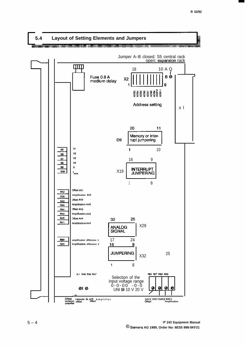
R 02/92
5.4 Layout of Setting Elements and Jumpers
5 – 4
Jumper A–B closed: S5 central rackopen: ex~ansion rack
i
x5
X6
X8
x9
Xlo
3
R42
R38
R39
R44
R40
R45
R41
3
R50
R49
PP 18 10 A Q
,Vl,V2
,V3
,V4
R
! ma
Offaat AVl
Amplification AVl
Y&4 AV2
hplification AV2
Maat AV3
hnplification AV3
)ffaat AV4
4mDlification AV4
amplification difference 1
knplifcation difference 2
‘9 %=31 10
16 9
X19n
INTERRUPTJUMPERING
1 8
17 24
r1 8
X29
X32
R81 R27 R82 R28
x l
25
R I R46 R46 R47
m
Selection of theinput voltage range
0@0 - 0 - 0 0 - 0 - 0
UNI Bi 10 V 20 Vm
0 0 0 0
Offaatiwlation W#ar Ei olar A m p l i f i e r#0 set
DAC2 DACI OAC2 OACIOrraat Amplification
amDlfier
1P 243 Equipment Manual
@ Siemens AG 1989, Order No: 6ES5 998-0KF21

R 02/92 Putting into Operation
5.5 Jumpering of the Analog Signals
5.5.1 Circuitry of the Analog Signal Jumpering
The two soldering bases X29 and X32 (see section 5.1) form the basis for the jumpering of theanalog signals. Via these bases, by means of soldering in jumpers, the required analog signals orthe different internal module components can be connected in a user–specific way.
The following diagram shows all signals on the jumpering base which can be combined.
Mma
Socket 6
Socket 5
Socket 4
Socket 3
Socket 2
Socket 1Pin Signal20 + 15 v21 – 15V23 M ~,24 AV125 AV226 AV327 AV4
r J II
IEll=lFllcomp’l *I +’-All +:AII+’-II+2-I
F109231 2112420 19 17 18
J
DAC131 21 ● 12 bits32
I 1 2 3 4 5 6 7 8
34 AlO35A1136A1237 A1338 A1439 A1540 A1641 A17
R+.rxv.
22 12 bits
30DAC38 bits
HHHH m l--Multiplexer
w I I
II e Chan. O- Chan. 1
m*
* Chan. 3- Chan. 4h Chan. 5
ADC12 bits
——
Diff.amp. = Difference amplificationComp. = ComparatorChan. = Channel
IP 243 Equipment Manual@ Siemens AG 1989, Order No: 6ES5 998-0KF21
5 – 5

Putting into Operation R 02/92
5.5.2 Soldering Base Pin Assignment
The analog signal jumpering comprises the two 16–way soldering base X29 and X32 (see section5.4, Layout of Setting Elements and Jumpers). The available 32 pins of the soldering bases havethe following signal assignment:
AR32: Socket 5 on front plate (free measuring wing point)AR31: Socket 6 on front plate Maria
I AR30: output of DAC3AR29: Analog output channel A05 via an output amplifier
AR28: Analog output channel A04
R
AR27: Analog output channel A03AR26: Analog output channel A02AR25: Analog output channel AO1
3231302928272625 I
1
—
2I Soldering base X29
-m’222324192(
AR19: Input comparator 1 “-comparator”
k~ AR24: Output difference amplifier 2AR23: Output difference amplifier 1AR22: output DAC2AR21 : Output DAC1AR20: Input comparator 1 “comparator”
AR18: Input comparator 2 “-comparator”AR17: Input comparator 2 “comparator”
5 – 6 1P 243 Equipment Manual@ Siemens AG 1989, Order No: 6ES5 998-0KF21

R 02/92 Putting into Operation
AR16: Output analog value conditioning AV1 socket 1
AR15: Output analog value conditioning AV2 socket 2
I AR14: Output analog value conditioning AV3 socket 3
AR13: Output analog value conditioning AV4 socket 4
I I I AR9: Input difference amplifier 1 “ –difference”1- i
AR12: Input difference amplifier 2” +difference”AR11: Input difference amplifier 2” –difference”
,—, AR1O: Input difference amplifier 1 “ +difference”
I 161514131211109 I3 4- n-) Soldering base X32
6 7 8
LI__ AR8: Analog input channel A17/channel 7 of ADCAR7: Analog input channel A16/channel 6 of ADCAR6: Analog input channel A15/channel 5 of ADCAR5: Analog input channel A14/channel 4 of ADCAR4: Analog input channel A13/channel 3 of ADCAR3: Analog input channel A12/channel 2 of ADCAR2: Analog input channel All/channel 1 of ADCAR1: Analog input channel AlO/channel O of ADC
All analog components are designed in a way that the signals at the analog signal jumpering arestandardized in the ranges O V tol O V or *1 O V.
1P 243 Equipment Manual
@ .%31WIS AG 1989, Order No: 6ES5 w8-0KF21
5 – 7

Putting into Operation R 02/92
5.6 Jumpering of the Binary Signals
The binary signals are also conducted via a soldering base and can be interswitched in a user–specific way. If desired, the interrupt evaluation is also activated via the binary signal jumpering.The digital inputs and outputs can be directly read in or read out via the bus. For interruptprocessing, however, jumpers must be installed on the soldering base X19. The followingdiagram shows the structure of the binary signal jumpering:
, r
$3 ~ ~ * - @ $- @ $ ~ @ ~ .$S5 bus
Pin SignalNo.
1 +24 V2 +24 V
11 6[0 Binary input O12 611 ● Binary input 1 w13 612 m Binary input 2 ?14 B13 D Binary input 3 Buffer15 B14 ● Binary input 4
16 B15 * Binary input 5
17 B16 o Binary input 6 :
18 617 Binary input 71 ,,1
~1
M
61 2 3 4 5
Comparator 1 D 10 InterruptComparator 2 D 9 Solci;~ng base 11 * driver _~G
12 forGating logic 2 D 8 S5-115U
D=13 - S5-135U -~D
Gating logic 1 ● 7 14“ ~%3;B *TC
15 andCPU 922)
-m16 -=
D9
1 0 6 0 7 ~42 Meti43 Mea
Binary output OBinary output 1Binary output 2Binary output 3Binary output 4Binary output 5Binary output 6Binarv outrwt 7
=1 6 Memory or
9 w%%$ase12 processing
-:: “MAT’CS5
5 – 8 1P 243 Equipment Manual
@ Siemens AG 1989, Order No: 6ES5 998-0KF21

R 02/92 Putting into Operation
5.7 Interrupt Jumpering
If an interrupt evaluation is intended, this is possible with the programmable controllersS5–11 5U/H and S5–135U with CPU 928A/B or CPU 922 (or same CPUS in PLC S5–155U) via direct busaccess to the interrupt lines. All other control devices require an additional binary input modulewith process interrupt generation and external wiring. In this case, the intermediate memory latchD9 must be replaced with the soldering base D9, included in the delivery. A detailed description ofthe procedures for interrupt processing with the 1P 243 is given in section 4. Here, reference ismade only to the pin assignment of the soldering base relevant to the jumpering of interrupts.
1,16+5 ‘t4 +3 W 11109
I1 2 3 4 5 6 7 8 I
1
>1
Interrupt line IR~Interrupt line IR~Interrupt line IR~lnterru~t line IR~Interrupt line IR~Interrupt line IR=
Output of comparator 1Output of comparator 2
Soldering base X19
Output of gating logic 2Output of gating logic 1
Grounding MBinary input B17
Binary input B16Binary input B15Binary input B14
Binary input B13
Binary input B12
Binary input Bll
Binary input BIO
Attention: At delivety, the jumpers are installed as shown in the diagram:
~ - ~ - ~ - ~ - ~ - ~ - M (P ins 16-15-14-13-11 -6 )
If the 1P 243 is used in SIMATIC S5 systems with Ievel–tri geredc?interrupt processing, these jumpers must not be change .
1P 243 Equipment Manual@SiemensA(31989, Order No: 6ES5998-0KF21
5 – 9

Putting into Operation
If. however, the module
R 02/92
is o~erated with a different rxo~rammable controller which allowinterrupt processing directly via the bus, then the corresponding pins of the interrupt lines must befree from their soldered connections. All unused interrupt lines must retain their jumperconnection with grounding M.
In the programmable controllerS5–115U, an interrupt is activated on interrupt line B via gatinglogic 1.
The following jumpers must be established on the soldering base:
— — — . ——IRA IRB IRC IRD IRF IRG Compl Cornpz
1.6 15 14 13.12.11 .10 !?
II I I
LkdL-1‘“1 2 3 4 5 6 7 8
BIo O V Bll O V B14 B15 B16 B17B12 O V 6130 V
M %!? gw
As already mentioned, for interrupt jumpering in SIMATIC S5 units without direct bus access,memory latch D9 must be replaced by the soldering base D9. This soldering base has thefollowing pin assignment:
120191817161514131211
Binary output B07Binary output B06Binary output B05Binary output B04
Soldering base D9
Binary output B03Binary output B02Binary output BO1Binary output BOO
Attention: To evaluate interrupts with an additional interrupt module, the interrupt–generating outputs of the comparators or the gating logic must be con-nected by jumpers from the soldering base Xl 9 to base D9 to the binaryoutputs of the 1P 243. These outputs are then connected externally to thebinary input module with process–interrupt generation.
5 – 10 1P 243 Equipment Manual
@ .%31TWS AG 1989, Order No: 6ES5 998-0KF21

R 02/92 Putting into Operation
5.8 Setting the Module Address
The module address is set via the DIP FIX switch on the soldering base X2 (see the layout of settingelements in section 5.4). Addressing in the 1/0 area is between the starting addresses 128 and248. The address displacement is 8 (i.e., a maximum of 16 modules can be addressed).
Example: First starting address 144Second starting address 152
It should be noted that when the 1P 243 is used in a central rack (S5–115U/H, S5–135U orS5–155U/H), the jumper A–B must be closed. In an expansion device, the jumper A–B I?WX
remain open.
The soldering base X2 appears as follows:
Address bit
ADB 3ADB 4ADB 5ADB 6ADB 7
ADB 8
ADB 9
ADB 10ADB 11
Jumper
1–182–173–164–155–14
6–13
7–12
8–1 19 – l o
Address
2 3 = 824 = 162 5 = 32
2 6 = 6 4
2 7 = 128{
2 6 = 256{
This jumper must always be installed in theP area as the module address is always ~128.
With SIMATIC S5, this “umper is only installeddwhen the module is a dressed in Q area.
2 9 = 512 ~
2 ’0 = 1024
J
With SIMATIC S5 these jumpers arealways open.
2“ = 2048
Attention: Only the programmable controllers S5–135U, S5–150U/SS5–155U/H are capable of addressing the Q area. The module must beinserted in an expansion rack. The Q area comprises the start adresses
1P 243 Equipment Manual
@ Siemens AG 1989, Order No: 6ES5 998-0KF215 – 11

Putting into Operation R 02/92
Addressing at the SIMATIC S5 system bus appears as follows:
SUB SUB SUBADB ADB ADB ADB ADB ADB ADB ADB ADB
,tix,,ins:+x ~:$‘-+‘::6n 4 3 - ;;: &!”&j\j’,i:-
:#J==:i;h:nQarea Module startin address7
section 7.5.)(jumper setting
Example: Setting of module address 144
10 – – – – – – –O 182 ()..__—41 7
30 – – – – – – –O 16
40 – – – – – – –o 1 5
5 o—————————— - 0 1 460 – – – – – – –O 13
70 – – – – – – –o 12
80 – – – – – – –O 11
90 – – – – – – –o 10
Base X2 assignment
5 – 12
ADB 3
ADB 4
ADB 5
ADB 6
ADB 7
ADB 8
ADB 9
ADB 10
ADB 11
@ Jumper 2 – 17 -t 24 = 16 and: p’ Jumper 5 – 14 -+27 = 128 installed
= 25 corresponds to the Sf3tthlg ‘nodule
= 26 address 144 (in the P areea)
= 27
= 28
= 29= 210
= 211
1P 243 Equipment Manual@ Siemens AG 1989, Order No: 6ES5 998-OKF21

R 02/92 Technical Specifications
6 Technical Specifications
Binary Inputs:
Rated Input Voltage . . . . . . . . . . . . . . . . . . . . . . . . . .Number oflnputs . . . . . . . . . . . . . . . . . . . . . . . . . . . .Galvanic Isolation . . . . . . . . . . . . . . . . . . . . . . . . . . . .Input Voltage Corresponding to:“O” Signal . . . . . . . . . . . . . . . . . . . . . . . . . . . . . . . . . . .“l” Signal , . . . . . . . . . . . . . . . . . . . . . . . . . . . . . . . . . .InputResistance . . . . . . . . . . . . . . . . . . . . . . . . . . . . .Input Current (’’l’’ Signal) . . . . . . . . . . . . . . . . . . . . .DelayTime . . . . . . . . . . . . . . . . . . . . . . . . . . . . . . . . . .Polarization Protection . . . . . . . . . . . . . . . . . . . . . . . .Maximum Permissible Cable Lengths:– Unshielded . . . . . . . . . . . . . . . . . . . . . . . . . . . . . . . .–Shielded . . . . . . . . . . . . . . . . . . . . . . . . . . . . . . . . . .Interrupt–Generating Inputs (Optional)
Binary Outputs:NumberofOutputs . . . . . . . . . . . . . . . . . . . . . . . . . . .Outputvoltage– Nominal Value . . . . . . . . . . . . . . . . . . . . . . . . . . . . .–ForSignal ”O” . . . . . . . . . . . . . . . . . . . . . . . . . . . . .–ForSignal ”l” . . . . . . . . . . . . . . . . . . . . . . . . . . . . .Output CurrentforSignal “1”– Nominal Value . . . . . . . . . . . . . . . . . . . . . . . . . . . . .– Permissible range . . . . . . . . . . . . . . . . . . . . . . . . . .Residual CurrentforSignal “O” . . . . . . . . . . . . . . . . .Total Switching Current . . . . . . . . . . . . . . . . . . . . . . .Switching FrequencywithoutLoad . . . . . . . . . . . . .Galvanic Isolation . . . . . . . . . . . . . . . . . . . . . . . . . . . .Fuse (Externa124VSupply) . . . . . . . . . . . . . . . . . . .Short-CircuitProtection . . . . . . . . . . . . . . . . . . . . . .Maximum Permissible Cable Lengths:–Unshielded . . . . . . . . . . . . . . . . . . . . . . . . . . . . . . . . .
24VDC8no
open–circuitedor –5Vto5.l V12.7vto30vtypically lOkQtypicaliy2.5mAtypicaily2.7msecyes
400m1000m
8
24Vmaximumof3Vminimum of–l.9V
200mA2t0200mAmaximumof250@maximumof600mAmaximumofl kHzno0.8 A, medium slowfuse
. . . . . . . . . . 400m–Shielded . . . . . . . . . . . . . . . . . . . . . . . . . . . . . . . . . . 1000m
lP243 EquipmentManual
@S@mensAG 1989,0rderN0:6ES5 998-0KF21
6 – 1

Technical Specifications R 02/92
Analog Inputs:Input Signal Ranges . . . . . . . . . . . . . . . . . . . . . . . . . . *5 V
+1 o v. . . . . . . . . . . . . . . . . . . . . . . . . . . . . . . . . —. . . . . . . . . . . . . . . . . . . . . . . . . . . . . . . . . o v to +10 v
Number of Inputs . . . . . . . . . . . . . . . . . . . . . .. .....8Digital Representation of Input Signal 11 bits and sign or 12 bitsMeasuring Principle . . . . . . . . . . . . . . . . . . . . . . . . . . successive approximationGalvanic Isolation . . . . . . . . . . . . . . . . . . . . . . . . . . . . noConversion Time . . . . . . . . . . . . . . . . . . . . . . . . . . . . .35 psec. 1Input Resistance . . . . . . . . . . . . . . . . . . . . . . . . . . . . . approximately 1 Mf2Permissible Voltage between Inputand Earth (Destruction Limit) . . . . . . . . . . . . . . . . . . *35 VMaximum Permissible Voltage betweenTwo Inputs (Destruction Limit) . . . . . . . . . . . . . . . . . . *35 VLinearity Error. . . . . . . . . . . . . . . . . . . . . . . . . . . . . . . . s ~3.1 0–4
Zero Error . . . . . . . . . . . . . . . . . . . . . . . . . . . . . . . . . . .< *5.1 0–4Temperature Error . . . . . . . . . . . . . . . . . . . . . . . . . . . .~ *3.1 0–5 pro KelvinBasic Error Limit (DIN 43745) . . . . . . . . . . . . . . . . . . stO.6%0Operational Error Limit
(between 0° C and +55° C) (DIN 43745) . . . . . . . s&l.2%.Maximum Permissible Cable Length–Shielded . . . . . . . . . . . . . . . . . . . . . . . . . . . . . . . . . . 20m
12-Bit Analog Output:Input Signal Range . . . . . . . . . . . . . . . . . . . . . . . . . . . *1O V bipolarNumber of Outputs . . . . . . . . . . . . . . . . . . . . . . . . . . . 2Digital Representation of Output Signal . . . . . . . . . 11 bits and signGalvanic Isolation . . . . . . . . . . . . . . . . . . . . . . . . . . . . noOutput Current . . . . . . . . . . . . . . . . . . . . . . . . . . . . . . . A5 mABurden Resistance . . . . . . . . . . . . . . . . . . . . . .. ....22 kQBurden Connection . . . . . . . . . . . . . . . . . . . . . . . . . . . burden connected to OVShort-Circuit Protection . . . . . . . . . . . . . . . . . . . . . . yesShort-Circuit Current . . . . . . . . . . . . . . . . . . . . . . . . .approximately 25 mASettling Time to 99% of Rated OutputValue for a Cable Length of 20 M .. . . . . .. .......5 psec.
Linearity Error. . . . . . . . . . . . . . . . . . . . . . . . . . . . . . . .< *3.1 0–4Zero Error . . . . . . . . . . . . . . . . . . . . . . . . . . . . . . . . . . . s ~5.10–4
Temperature Error . . . . . . . . . . . . . . . . . . . . . . . . . . . .<*2.1 0–6 pro KelvinBasic Error Limit (DIN 43745) . . . . . . . . . . . . . . . . . . <&O.6%0Operational Error Limit(between 0° C and +55° C DIN 43745) . . . . . . . . . s~O.85%0Maximum Permissible Cable Length–Shielded . . . . . . . . . . . . . . . . . . . . . . . . . . . . . . . . . . 20m
I Thecommand processingtimes for the selection ofmeasuring points and thestart of coding are notincluded here.
6 – 2 1P 243 Equipment Manual
@ Siemens AG 1989, Order No: 6ES5998-OKF21

R 02/92 Technical Specifications
8–Bit Analog Output:Output Signal Range . . . . . . . . . . . . . . . . . . . . .. ...0 V to +10 V, unipolarNumber of Outputs . . . . . . . . . . . . . . . . . . . . . . . . . . . 1Digital Representation ofOutput Signal . . . . . . . . . . . . . . . . . . . . . . . . .. ......8 bitsGalvanic Isolation . . . . . . . . . . . . . . . . . . . . . . . . . . . . noOutput Current . . . . . . . . . . . . . . . . . . . . . . . . . . . . . . . *5 mABurden Resistance . . . . . . . . . . . . . . . . . . . . ... ... .>2 kQBurden Connection . . . . . . . . . . . . . . . . . . . . . . . . . . . burden connected to O VShort-Circuit Protection . . . . . . . . . . . . . . . . . . . . . . temporaryShort-Circuit Current . . . . . . . . . . . . . . . . . . . . . . . . . undefinedSettling Time tO 9W0 OfRated Output Value for aCable Length of 20 M . . . . . . . . . . . . . . . . . . . . . . . . . 10 psec.Basic Error Limit (DIN 43765) . . . . . . . . . . . . . . . . . . s*2%Operational Error Limit
(between 0° C and +55° C) (DIN 43765) . . . . . . . . s*4%Maximum Permissible Cable Length–Shielded . . . . . . . . . . . . . . . . . . . . . . . . . . . . . . . . . . 20m
Analog Output AmplifierOutput Signal Range . . . . . . . . . . . . . . . . . . . . . . . . . A1OV bipolarNumber of Outputs . . . . . . . . . . . . . . . . . . . . . . . . . . . 1Galvanic Isolation . . . . . . . . . . . . . . . . . . . . . . . . . . . . noOutput Current . . . . . . . . . . . . . . . . . . . . . . . . . . . . . . . .i5 mABurden Resistance . . . . . . . . . . . . . . . . . . . . . .. ....22 kQBurden Connection . . . . . . . . . . . . . . . . . . . . . . . . . . . burden connected to O VShort-Circuit Protection . . . . . . . . . . . . . . . . . . . . . . yesShort-Circuit Current . . . . . . . . . . . . . . . . . . . . . . . . .approximately 20 mAMaximum Permissible Cable Length–Shielded . . . . . . . . . . . . . . . . . . . . . . . . . . . . . . . . . . 20m
8–Bit Analog Output with Analog Amplifier Series:Output Signal Range . . . . . . . . . . . . . . . . . . . . . . . ..0 Vto 10 Y unipolarNumber of Outputs . . . . . . . . . . . . . . . . . . . . . . . . . . . 1Digital Representation . . . . . . . . . . . . . . . . . . . . . . . . 8 bitsGalvanic Isolation . . . . . . . . . . . . . . . . . . . . . . . . . . . . noOutput Current . . . . . . . . . . . . . . . . . . . . . . . . . . . . . . . L5 mABurden Resistance . . . . . . . . . . . . . . . . . . . . . . .. ....22 k!2Burden Connection . . . . . . . . . . . . . . . . . . . . . . . . . . . burden connected to O VShort-Circuit Protection . . . . . . . . . . . . . . . . . . . . . . yesShort-Circuit Current . . . . . . . . . . . . . . . . . . . . . . . . . approximately 20 mASettling Time to 99% of Rated OutputValue for a Cable Length of 20 M . . . . . . . . . . . . . . . 10 psec.
Error Limit at 25° C . . . . . . . . . . . . . . . . . . . . . . . . . . . s ~0.2%
Error Limit between 0° C and +55° C s tO.4Y0Maximum Permissible Cable Length–Shielded . . . . . . . . . . . . . . . . . . . . . . . . . . . . . . . . . . 20m
1P 243 Equipment Manual
@ Siemens AG 1989, Order No: 6ES5 998-0KF21
6 – 3

Technical Specifications R 02/92
Analog Value Conditioning Circuits:Input Signal Range . . . . . . . . . . . . . . . . . . . . . . . . . . . ~10 VNumber oflnputs . . . . . . . . . . . . . . . . . . . . . . . . . . . . 4Galvanic Isolation . . . . . . . . . . . . . . . . . . . . . . . . . . . . noInput Resistance . . . . . . . . . . . . . . . . . . . . . . . . . . . . . typically 200 kQInput Time Constant . . . . . . . . . . . . . . . . . . . . . . . . . . typically 110 psec.Setting Range for Zero Displacement –2 Vto +2 V(Operating Point)Amplification . . . . . . . . . . . . . . . . . . . . . . . . . . . . . . . . . 0.5 to 5Voltage between Input and0 V Connection (Destruction Limit) . . . . . . . . . . . . . maximum .&35 V
Difference Amplifier (P controller):Input Signal Range . . . . . . . . . . . . . . . . . . . . . . . . . . . ~10 VOutput Signal Range . . . . . . . . . . . . . . . . . . . . . . . . . A1OVNumber of Controllers . . . . . . . . . . . . . . . . . . . . . . . . 2Galvanic Isolation . . . . . . . . . . . . . . . . . . . . . . . . . . . . noOutput Current . . . . . . . . . . . . . . . . . . . . . . . . . . . . . . . &5 mAAmplification. . . . . . . . . . . . . . . . . . . . . . . . . . . . . . . . . 1.1 to 20Input Time Constant . . . . . . . . . . . . . . . . . . . . . . . . . . typically 500 psec.Input Resistance . . . . . . . . . . . . . . . . . . . . . . . . . . . . . typically 1 MQBurden Resistance . . . . . . . . . . . . . . . . . . . . . . . . . . . 22 kQShort-Circuit Protection . . . . . . . . . . . . . . . . . . . . . . yesShort-Circuit Current . . . . . . . . . . . . . . . . . . . . . . . . .approximately 50 mAVoltage between Two Inputs(Destruction Limit) . . . . . . . . . . . . . . . . . . . . . . . . . . . . *35 VVoltage between input and0 V connection (Destruction Limit) . . . . . . . . . . . . . . *35 V
Comparators:Input Signal Range . . . . . . . . . . . . . . . . . . . . .. .....0 V to +10 VNumber oflnputs . . . . . . . . . . . . . . . . . . . . . . . . . . . . 2Input Time Constant . . . . . . . . . . . . . . . . . . . . . . . . . . typically 250 psec.Input Resistance . . . . . . . . . . . . . . . . . . . . . . . . . . . . . typically44 kQVoltage between Two Inputs(Destruction Limit) . . . . . . . . . . . . . . . . . . . . . . . . . . . . maximumi35 VVoltage between Input andOVConnection (Destruction Limit) . . . . . . . . . . . . . ~35VInterrupt–Generating Option
6 – 4 1P 243 Equipment Manual@ Siernens AG 1989, order No: 6E.S5998-I)KF21

R 02/92 Technical Specification
Power Supply Voltage UP:Rated value . . . . . . . . . . . . . . . . . . . . . . . . . . . . . . . . . 24VDCRipple U~~ . . . . . . . . . . . . . . . . . . . . . . . . . . . . . . . . . . . maximum 3.6 VPermissible Range (Including Ripple) .. . . .......20 Vto 30 V DCValue for t e 0.5 sec. . . . . . . . . . . . . . . . . . . . . . . . . . maximum 35V
Current Consumption:Internal +5 V Supply . . . . . . . . . . . . . . . . . . . . . . . . . typically 600 mAExternal +24 V Supply(without Sensor Power Supplyand Total Switching Current) . . . . . . . . . . . . . . . . . . . typically 270 mAExternal Supply Voltage . . . . . . . . . . . . . . . . . . . . . . . +20 V DC to +30 VPower Loss–Full Configuration . . . . . . . . . . . . . . . . . . . . . . . . . . . 11.8 W(6ES5243-lAA1 1)–Part Configuration, Al Only .. .................4.6 W(6ES5243-lAB1l)–Part Configuration, AO Only .. ................6.1 W(6ES5243-lACI 1)
Mechanical Data:Dimensions (W x H x D) . . . . . . . . . . . . . . . . . . . . . . . 20 mm x 244 mm x 202 mmMounting Width . . . . . . . . . . . . . . . . . . . . . . . . . . . . . . 1–1/3 SPS = 1 module slot
Weight . . . . . . . . . . . . . . . . . . . . . . . . . . . . . . . . . . . . .approximately 0.46 kg (6ES5243-lAA11). . . . . . . . . . . . . . . . . . . . . . . . . . . . . . . . . . . . . . .approximately 0.38 kg (6ES5243–lAB11). . . . . . . . . . . . . . . . . . . . . . . . . . . . . . . . . . . . . . .approximately 0.39 kg (6ES5 243–1AC11 )
Ambient Conditions:
Operating Temperature . . . . . . . . . . . . . . . . . . . . . . . 0° to +55° C
Storage and Transport Temperature . . . . . . . . . . . . –40° to +70° C
1P 243 Equipment Manual@ Siemens AG 1989, Order No: 6ES5 998-0KF21
6 – 5
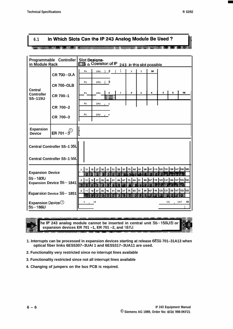
Technical Specifications R 02/92
6.1
Programmable Controller Slot Designa-in Module Rack _ Q ORerationoflp 243 inthkslot~ossible
Ps CPU I o I 1 2 3 IM
CR 700–OIA
Ps CPU I oCR 700–OLB
CentralController Ps CPU
CR 700–1S5–115U
Ps CPU I o
CR 700–2
Ps CPU I oCR 700–3
ExpansionDevice
Central Controller S5–1 35L
Central Controller S5–1 55L
3Expansion Device
S5–183UExpansion Device S5– 1841
Expansion Device S5– 1851
Expansion Device@ 3I
19 131I
147 63
S5–186U 1
: The 1P 243 analog module cannot be inserted in central unit S5–150U/S or in ‘:expansion devices ER 701 –1, ER 701 –2, and 187U.
1. Interrupts can be processed in expansion devices starting at release 6ES5 701–31A13 whenoptical fiber links 6ES5307–3UAI 1 and 6ES5317–3UA11 are used.
2. Functionality very restricted since no interrupt lines available
3. Functionality restricted since not all interrupt lines available
4. Changing of jumpers on the bus PCB is required.
6 – 6 1P 243 Equipment Manual@ Siemens AG 1989, Order No: 6ES5 998-0KF21

R 02/92 Table of Contents
7.1
7.27.2.17.2.27.2.37.2.47.2.57.2.67.2.7
7.37.3.17.3.27.3.37.3.47.3.57.3.67.3.7
7.47.4.17.4.27.4.37.4.47.4.57.4.67.4.77.4.87.4.9
7.57.5,17.5.2
Overview . . . . . . . . . . . . . . . . . . . . . . . . . . . . . . . . . . . . . . . . . . . . . . . . . . . . . . . .
Function Block FB160(PER:ANL) . . . . . . . . . . . . . . . . . . . . . . . . . . . . . . . . .Function Description . . . . . . . . . . . . . . . . . . . . . . . . . . . . . . . . . . . . . . . . . . . . . . .Calling the Function Block . . . . . . . . . . . . . . . . . . . . . . . . . . . . . . . . . . . . . . . . . .Explanation ofParameters . . . . . . . . . . . . . . . . . . . . . . . . . . . . . . . . . . . . . . . . . .ParameterAssignment . . . . . . . . . . . . . . . . . . . . . . . . . . . . . . . . . . . . . . . . . . . . .Data AreaAssignment . . . . . . . . . . . . . . . . . . . . . . . . . . . . . . . . . . . . . . . . . . . . .Technical Specifications . . . . . . . . . . . . . . . . . . . . . . . . . . . . . . . . . . . . . . . . . . . .Function BlockApplication . . . . . . . . . . . . . . . . . . . . . . . . . . . . . . . . . . . . . . . . .
Function Block FB161 (PER:ANS) . . . . . . . . . . . . . . . . . . . . . . . . . . . . . . . . .Function Description . . . . . . . . . . . . . . . . . . . . . . . . . . . . . . . . . . . . . . . . . . . . . . .Calling the Function Block . . . . . . . . . . . . . . . . . . . . . . . . . . . . . . . . . . . . . . . . . .Explanation ofParameters . . . . . . . . . . . . . . . . . . . . . . . . . . . . . . . . . . . . . . . . . .ParameterAssignment . . . . . . . . . . . . . . . . . . . . . . . . . . . . . . . . . . . . . . . . . . . . .Data AreaAssignment . . . . . . . . . . . . . . . . . . . . . . . . . . . . . . . . . . . . . . . . . . . . .Technical Specifications . . . . . . . . . . . . . . . . . . . . . . . . . . . . . . . . . . . . . . . . . . . .Function BlockApplication . . . . . . . . . . . . . . . . . . . . . . . . . . . . . . . . . . . . . . . . .
Example . . . . . . . . . . . . . . . . . . . . . . . . . . . . . . . . . . . . . . . . . . . . . . . . . . . . . . . . .Device Configuration. . . . . . . . . . . . . . . . . . . . . . . . . . . . . . . . . . . . . . . . . . . . . . .JumperAssignmentoftheAnalog Module . . . . . . . . . . . . . . . . . . . . . . . . . . . .Assignmentofthe lnputsand Outputs . . . . . . . . . . . . . . . . . . . . . . . . . . . . . . .Turn–On, Start-UpBehavior . . . . . . . . . . . . . . . . . . . . . . . . . . . . . . . . . . . . . . .Reading the Binarylnputs . . . . . . . . . . . . . . . . . . . . . . . . . . . . . . . . . . . . . . . . . .Reading theAnalogValue . . . . . . . . . . . . . . . . . . . . . . . . . . . . . . . . . . . . . . . . . .Checking theComparators . . . . . . . . . . . . . . . . . . . . . . . . . . . . . . . . . . . . . . . . .Writing the Binary Outputs . . . . . . . . . . . . . . . . . . . . . . . . . . . . . . . . . . . . . . . . . .Writing theAnalogValue . . . . . . . . . . . . . . . . . . . . . . . . . . . . . . . . . . . . . . . . . . .
ProgrammingWithoutFB . . . . . . . . . . . . . . . . . . . . . . . . . . . . . . . . . . . . . . . . .AddressAssignment . . . . . . . . . . . . . . . . . . . . . . . . . . . . . . . . . . . . . . . . . . . . . . .Reading and Writingthelnputs and Outputs . . . . . . . . . . . . . . . . . . . . . . . . . .
7 – 1
7 – 27 – 27 – 27 – 37 – 47 – 47 – 57 – 6
7 – 77 – 77 – 77 – 87 – 87 – 9
7 – l o7 – 1 1
7 – 1 27 – 1 27 – 1 37 – 1 47 – 1 57 – 1 57 – 1 67 – 1 77 – 1 77 – 1 8
7 – 1 97 – 1 97 – 2 0
lP248 EquipmentManual
@SiemensAG 1989, OrderNo: 6ES5998-0KF21
7 – 1
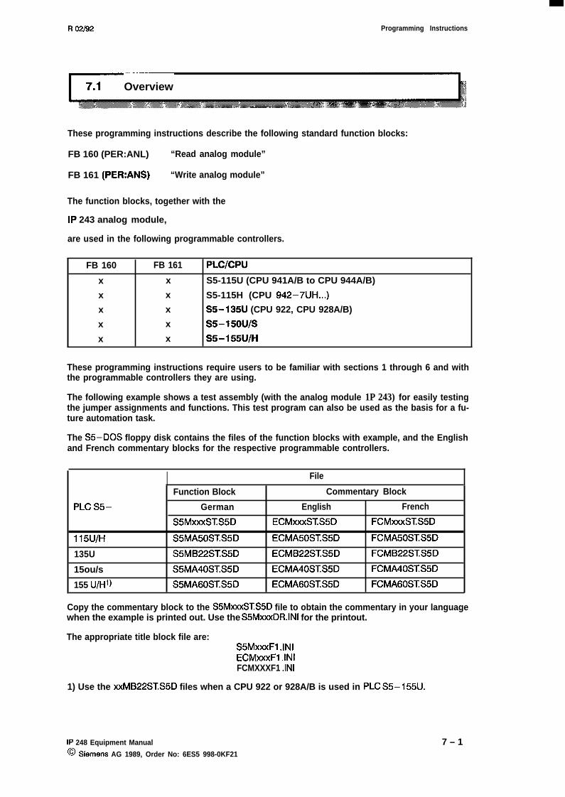
R02/92 Programming Instructions
7.1 Overview
These programming instructions describe the following standard function blocks:
FB 160 (PER:ANL) “Read analog module”
FB 161 (PER:ANS) “Write analog module”
The function blocks, together with the
1P 243 analog module,
are used in the following programmable controllers.
FB 160 FB 161 PLC/CPU
x x S5-115U (CPU 941A/B to CPU 944A/B)
x x S5-115H (CPU 942–7UH...)
x x S5-135U (CPU 922, CPU 928A/B)
x x s5-150u/s
x x S5-155U/H
These programming instructions require users to be familiar with sections 1 through 6 and withthe programmable controllers they are using.
The following example shows a test assembly (with the analog module 1P 243) for easily testingthe jumper assignments and functions. This test program can also be used as the basis for a fu-ture automation task.
The S5–DOS floppy disk contains the files of the function blocks with example, and the Englishand French commentary blocks for the respective programmable controllers.
I File
Function Block Commentary Block
PLC S5– German English French
S5MXXXSTS5D ECMXXXSTS5D FCMXXXSTS5D
115U/H S5MA50ST.S5D ECMA50ST.S5D FCMA50ST.S5D
135U S5MB22ST.S5D ECMB22ST.S5D FCMB22STS5D
15ou/s S5MA40STS5D ECMA40ST.S5D FCMA40STS5D
155 U/Ht) S5MA60ST.S5D ECMA60ST.S5D FCMA60ST.S5D
Copy the commentary block to the S5MXXXSTS5D file to obtain the commentary in your languagewhen the example is printed out. Use the S5MXXXDR.INI for the printout.
The appropriate title block file are:S5MX)O(F1 .INIECMXXXF1 .INIFCMXXXF1 .INI
1) Use the XXMB22STS5D files when a CPU 922 or 928A/B is used in PLC S5–155U.
1P 248 Equipment Manual
@ .%311WIS AG 1989, Order No: 6ES5 998-0KF21
7 – 1

Programming Instructions R 02/92
7.2 Function Block FB 160 (PER:ANL)
7.2.1 Function Description
The function block “Read analog module” (when the module is outfitted accordingly) accepts theselected analog value and outputs it either as a bit pattern, the way it arrives from the module, or asa 16–bit fixed point numeral, standardized to the respective nominal value.
Furthermore, the binary inputs and the comparator outputs can be read with this function block.Prior to reading the comparator outputs, the gating logic is switched over.
Function
FB 160 reads the analog and binary inputs, switches over the gating logic and reads the com-parator outputs.
7.2.2 Calling the Function Block
In the STL (statement list):
S5-115U/H
NAMEBGKNBTNORMDELKP LLOGSTRADUDEKOMPPAFE
:JU FB160:PER:ANL
S5–135Us5-150u/sS5-155U/H
:JU FB160NAME :PER:ANLBGKN :P/Q :BT :NORM :DEL :KP L :LOG :STR :ADU :DE :KOMP :PAFE :
In the IAD/CSF (Ladder diagram/control system flowchart)
FB 160PER:ANL
— BGKN ADU— BT DE— NORM KOMP —— DEL PAFE —— KP L— LOG— STR
FB ~60PER:ANL
— BGKN ADU— P/Q DE— BT KOMP —— NORM PAFE —— DEL— KP L— LOG— STR
7 – 2 1P 243 Equipment Manual
@ %3fIN3flS AG 1989, Order No: 6ES5 998-0KF21

R 02/92 Programming Instructions
7.2.3 Explanation of Parameters
I NAME I CLASSI TYPE I DESIGNATION II BGKNI D I K Y I Specificationof themoduleaddressand c h a n n e l n u m b e r I
I P/Q I D I KS I Specification ofl/Oarea ‘
I BT I D I ‘F I Specification of module type (nominal range)
I NORMI I I BI I Switchovertoinputof standardizedvalues II DEL I I I BI I Readdigitalinputs II KPL I I I BI I Readcomparatoroutputs I
I LOG ! I ! BI ! Switching over the gating logicI
I STR I 1 I BI I Enable signal forcomparator interrupt II ADU I Q I W I Analogvalueoutput II DE I Q I BY I Outputtingthedi$jitalinputs II KOMPI Q I B Y I Outputtingthecomparatoroutputs II PAFE I Q I Parameterization error
1 This parameter is not available on the S5–115U/Haddressed in the P area.
1P 248 Equipment Manual
@ Siemens AG 1989, Order No: 6ES5 998-0KF21
programmable controller. It can only be
7 – 3

Programming Instructions R 02/92
7.2.4 Parameter Assignment
BGKN : KY = x, y x = Module address128< X ~ 248 for P/Q : KS=P
0< X <248 for P/Q: KS=Q
y = Channel numbero5y57
P/Q :
BT :
PAFE :
KS = P Normal 1/0 areaKS = Q Expanded 1/0 area
KF = X Module type; Specification of the nominal rangex = O unipolar O V to 10 vx = 1 bipolar –10 V to +10 Vx = 2 bipolar –5 V to +5 V
In case of illegal parameterization the signal status is”1”. The recog–nized error is then shown by the assignment of the flag byte FY 255:
F 255.0
F 255.1
F 255.2
F 255.3
F 255.4
F 255.5
F 255.6
F 255.7
The module address is outside of the specified area or isnot within the 8–bit grid pattern(first part of parameter BGKN)
The parameter P/Q is not set with ‘P-’ or ‘Q-’.(Does not apply to programmable controller S5-115U/H.)
—
—
QVZ, no module found under this address.(first part of parameter BGKN)(only set with S5-155U/H)
—
The channel number is outside the specified range(second part of parameter BGKN)
The parameter BT is outside the specified range.
7.2.5 Data Area Assignment
No data blocks are addressed.
Addressing the Module in S5–155/H
For proper operation of the function block, the analog module 1P 243 must be addressed in theaddress range from KH = FF080 to KH = FF1 FE This corresponds to the 1/0 area fromKH = FF080 to KH = FFOFF (byte number 128 to 255) and to the Q range from KH = FF1OO toKH = FF1 FF (byte number O to 255).
7 – 4 1P 243 Equipment Manual@ Siemens AG 1989, Order No: 6ES5 998-0KF21

R 02/92
7.2.6 Technical Specifications
Programming Instructions
Block no. 160
Block name PER:ANL
PLC S5– 115U 135U 15ou/s 155U
Library no. P71200–S... 51 60–A–2 9160–A–1 4160–A–1 61 60–6–1
Call length (in words) 13 14
Block length (in words) 165 180 222
Processing time(in msec)
CPU 941A/B CPU 922Without standardization 8.2/4.9 1.8 0.4 0.69With standardization 11.115.9 2.1 0.5 0.74
CPU 942A/B CPU 928A/BWithout standardization 5.4/4.9 1 .1/1.0With standardization 6.4/5.9 1 .2/1.1
CPU 943A/BWithout standardization 3.3/4.1With standardization 4.5/5.5
CPU 944A/BWithout standardization 0.5/0.3With standardization 2.1/1 .7
Nesting depth 1 0
Blocks called FB 242 (inte- Nonegrated inPLC)
Data areas used —
Flag areas used FY 238 to FY 244 to FY 255FY 255
System instructions None
Other 1) I—
I 2)
1) Interruptions (interrupts and wake–up alarms) are temporarily disabled in the block with theAS/AF commands. This cancels out any “AS” command which you may have programmed.
2) All interruptions (process alarms, interrupts and wake–up alarms) are disabled in the blockfor approximately 42 pee.
1P 243 Equipment Manual@ Siemens AG 1989, Order No: 6ES5 998-0KF21
7 – 5

Programming Instructions R 02/92
7.2.7 Function Block Application
The module basic address and the channel number for the analog value are specified by parame-ter BGKN. Depending on the channel number, the function block reads an analog value from themodule and outputs it at parameter ADC.
The representation of the analog value depends on the NORM parameter:
NORM = “O”:
The analog value read at the module is output unchanged at parameterADC (as abit pattern according to the description in the operating instructions).
NORM = “1“
The analog value read at the module is converted to the nominal range. The nomi-nal range is defined by the values at parameter BT The conversion formulas are:
for BT = O (Nominal range O V to 10 V):20000
ADC = rough value x ~192
for BT = 1 (Nominal range –10 Vto +10 V):20000
ADC = rough value x ~096
for BT = 2 (Nominal range –5 V to +5 V):20000
ADC = rough value x ~192
The analog value is output as a 16–bit fixed–point numeral for the unit mv.
When parameter DE–L has the signal status”1”, the binary module inputs are read and then out-put at parameter DE. If the module has no binary inputs, signal status “O” is output to all bits.
When parameter KP–L has the signal status”1”, the comparator outputs of the module are readand then output at parameter KOMI? The bits now required, LOG and STR, are set in accordancewith the parameters LOG and STR, and they are transferred to the module during channel selec-tion.
7 – 6 1P 243 Equipment Manual@ Siemens AG 1989, Order No: 6ES5 998-0KF21

R 02/92 Programming Instructions
7.3 Function Block FB 161 (PER:ANS)
7.3.1 Function Description
The function block “Write analog module” either transfers a specified bit pattern or a 16–bitfixed–point numeral, standardized to the nominal value, to the module. The function block canalso control the binary outputs if the module is outfitted accordingly.
Function
FB 161 outputs an analog value and the 8 binary outputs.
7.3.2 Calling the Function Block
In the STL (statement list):
S5-115U/H
:JU FB161NAME :PER:ANSBGKN :NORM :DAC :DAS :DA :PAFE :
In the IAD/CSF (Ladder diagram/control system flowchart):
FB 161
n
PER:ANSBGKN PAFENORMDACDASDA
S5-135U, S5-150U/S, S5–155U/H
:JU FB161NAME :PER:ANSBGKN :P/Q :NORM :DAC :DAS :DA :PAFE :
FB 161
r
PER:ANSBGKN PAFEP/QNORMDACDASDA
1P 243 Equipment Manual
@ Siemens AG 1989, Order No: 6ES5 998-0KF217 – 7

Programming Instructions R 02/92
7.3.3 Explanation of Parameters
NAME I CLASS I TYPE I DESIGNATION1 1 I I
BGKN I D ! KY ! Specification of the module address and channel numberI .
P/Q I D I KS I Specification of 1/0 area ‘ I
NORM I I I BI I Switchovertoinputof standardizedvalues I1
DAU I w Specification of the 1/0 area
DAS I BI Write digital outputs
DA I BY Specification of the digital outputs1 ,
PAFE Q I BI I Parameterization error I1 This parameter is not available on the S5–1 ICW+ Pmwrnrnable controller. [t can oniY be
addressed in the P area.
7.3.4 Parameter Assignment
BGKN : KY = X, y x = Module address128< X <248 for P/Q : KS=PO <X< 248 for P/Q: KS=Q
P/Q :
PAFE :
y = Channel numbero<y57
KS = P Normal 1/0 areaKS = Q Extended 1/0 area
In the event of illegal parameterization, the signal status is”1”. There-cocmized error is then indicated bv the assignment of the flag byteFY-255:
F 255.0
F 255.1
F 255.2
F 255.3
F 255.4
F 255.5
F 255,6
F 255.7
The module address is outside the specified area ornot within the 8–bit grid pattern.(first part of parameter BGKN)
The parameter is not set with ‘P-’ or ‘Q–’.(Does not apply to programmable controllerS5-115U/H)
—
—
QVZ, no module found under this address.(first part of parameter BGKN)(only set with S5-155U/H)
—
The channel number is outside the specified range(second part of parameter BGKN)
—
7 – 8 1P 243 Equipment Manual@ Siemens AG 1989, Order No: 6ES5 998-0KF21

R 02/92 Programming Instructions
7.3.5 Data Area Assignment
No data blocks are addressed.
Addressing the Module (S5–155U/H)
For proper operation of the function block, the analog module 1P 243 must be addressed in theaddress range from KH = FF080 to KH = FF1 FE This corresponds to the 1/0 area fromKH = FF080 to KH = FFOFF (byte number 128 to 255) and to the Q range from KH = FF1OO toKH = FFIFF (byte number O to 255).
1P 248 Equipment Manual
@ .%3TWIS AG 1989, Order No: 6ES5 998-0KF21
7 – 9

Programming Instructions
7.3.6 Technical Specifications
R 02/92
0 . 5 90 . 6 4
Block no. 161
Block name PER:ANS
PLC S5– 115U 135U 150UIS 155U
Library no. P71200–S... 5161 –A–O 9161 –A–1 4161 –A–O 6161 –B–1
Call length (in words) 8 9
Block length (in words) 158 170 195
Prcessing time(in msec)
CPU 941A/B CPU 922Without standardization 5.9/3.2 1.4 0.2 IWith standardization 9.6/3.5 1.7 0.3 (
CPU 942A/B CPU 928A/BWithout standardization 3.3/3.2 0.7/0.2With standardization 4.4/3.5 1 .0/0.3
CPU 943A/BWithout standardization 2.8/2.6With standardization 3.1/2.8
CPU 944A/BWithout standardization 0.3/< 0.1With standardization 1.811.6
Nesting depth 1 0
Blocks called FB242(inte- Nonegrated inPLC)
Data areas used —
Flag areas used FY 238 to FY 248 to FY 255FY 255
System instructions None
Other —
7 – 1 0 1P 243 Equipment Manual
@ sk311W3flS AG 1989, Order No: 6ES5 998-0KF21

R 02/92 Programming Instructions
7.3.7 Function Block Application
The module basic address and the channel number of the analog value to be writien are specifiedat parameter BGKN. The value at parameter DAU is transferred to DAC1, DAC2, or DAC3 accord-ing to the channel number.
The representation of the analog value DAC depends on the signal status at parameter NORM:
NORM = “O”:
The bit pattern at parameter DAC (in the case of channel 3, the left byte) is trans-ferred to the module unchanged (bit assignment as shown in the operating in-structions).
NORM = “1“:
The value at the parameter is interpreted as a standardized 16–bit fixed–pointnumber (nominal range with KN = 1 or 2: * 10000 mV; with KN = 3: O to 10000rev). Depending on the channel number KN, the analog value is computed ac-cording to the following formula:
For channel number 1 or 2:13422
Analog va lue = DAC x —65536
For channel number 3:1678
Analog va lue = DAC x —65536
If the value is outside the currently valid nominal range, it is limited to an extremevalue.
If the parameter DA-S has signal status”1”, the value at parameter DA is transferred to the binarymodule outputs. If the module has no binary outputs, the command is ineffective.
1P 243 Equipment Manual@ Siemens AG 1989, Order No: 6ES5 998-0KF21
7 – 11

Programming Instructions R 02/92
This example shows the operation of the analog module 1P 243. By means of a simulator the indi-vidual functions can be selected (via binary inputs). The signal states can be displayed via binaryoutputs. The display shows how an analog value applied to the module can be read and how ananalog value can be output via the module.
This example also shows the necessary jumper settings and wiring requirements for the mo-dule.Therefore, it can also be used as a test program to check the jumper settings and functions of themodule.
7.4.1 Device Configuration
For a test of the analog module 1P 243, the following devices can be used:
– One of the listed programmable controllers
– Programmer (e.g., PG 750)
– Analog module 1P 243 (6ES5 243–lAA11) in full configuration: front connector K with screwmounting (6)(X3 081)
– Digital input module; front connector with screw mounting
– Digital output module; front connector with screw mounting
– 2 simulators (6ES5788–0L412)
– Voltage source for two analog signals
– Voltmeter
7 – 12 1P 243 Equipment Manual
@ .%31W31S AG 1989, Order No: 6ES5 998-0KF21

R 02/92 Programming Instructions
7.4.2 Jumper Assignment of the Analog Module
Module Address (Basic Address 160):
DIP switch S2: ABD 5 ON[Jumper 3–16 = 25 = 3 2
ABD 7 ON IJumper 5–14 = 27 =128Module address z
18 17 16 15 14 13 12 11 10
x2
1 2 3 4 5 6 7 8 9
Analog routing:
Soldering bases X32 and X29:
Analog value 1 – > Channel O –> Comparator 1 +(PIN 16) (PIN 2) (PIN 20)
Analog value 2 – > Channel 1 –> Comparator 1 –(PIN 15) (PIN 2) (PIN 19)
DAC1 – > AQ1(PIN 21) (PIN 25)
DAC2 –> AQ2(PIN 22) (PIN 26)
DAC3 –> AQ3(PIN 30) (PIN 27)
1P 243 Equipment Manual
@ .%311WflS AG 1989, Order No: 6ES5 998-0KF217 – 13

Programming Instructions R 02/92
7.4.3 Assignment of the Inputs and Outputs
The program is designed in a way that allows easy adaptation to different input and output assign-ments. The program block (PB 243) that contains the test program works with flags only. The in-puts and outputs to be used are allocated to these flags by organization block OB 1.
In the example the flags are the input word IW4 and the output word QW4 or the input word IW4and the output word QW8 for theS5–115U.
I 4.0I 4.114.2I 4.3I 4.4
I 4.514.6I 4.7
IB5
QB4/QB8
QB5/QB9
Q 6. O/Q 10.0Q 6.1/Q 10.1
————
F 4.0F 4.1F 4.2F 4.3F 4.4
F 4.5F 4.6F 4.7
FY5
FY8
FY 9
F 14.0F 14.1
FW 10FW 12FY 16FY 17
NORMDE LKP:LLOGSTR
—DA-S
DA
DE
KOMP
PAFEPAFE
ADUDAU
Standardize analog value (convert)Read binary inputsRead comparator outputsSwitch over gating logicEnable signal for comparator interrupt
—Write binaty outputsReset all binary outputs and flags
Binary outputs for output via the analog module
Binary inputs read by the analog module
Comparator outputs read by the analog module
Parameterization error bit of FB 160Parameterization error bit of FB 161
Analog value read by the moduleAnalog value output via the moduleError flag byte (FY 255) of FB 160Error flag byte (FY 255) of FB 161
7 – 14 1P 243 Equipmant Manual
@ Siemens AG 1989, Ordar No: 6ES5 998-0KF21

R 02/92 Programming Instructions
7.4.4 Turn-On, Start-Up Behavior
The program is loaded entirely from the floppy disk to the user memory of the programmable con-troller.
During start-up there is no need to supply any data to the analog module. Its ready state is indi-cated by the green LED on the front panel. The LED lights up when an external 24 V voltage isapplied.
If at the time the programmable controller is turned on, all simulator inputs are in switch position“O”, no outputs maybe set after the start-up of the programmable controller.
If one of the outputs Q 6. O/Q 10.0 (flag F 14.0) or Q 6.1/Q 10.1 (flag F 14.1) is set, a para-meteriza-tion error was made. The exact error cause can be identified at flag byte FY 16 (for theparameterization error shown for output Q 6. O/Q 10.0) or at flag byte FY 17 (for the parametrizat-ion error shown for output Q 6.1/Q 10.1). Both flag bytes are set in accordance with the error bytesFY 255 of the standard function blocks FB 160 and FB 161.
7.4.5 Reading the Binary Inputs
If input 14.1 is brought to switch position”1”, the binary inputs connected to the analog moduleare displayed at output byte QB4/QB8. If the signal status of these inputs is modified, the displayon the simulator is modified accordingly.
1P 243 Equipment Manual
@ Siemens AG 1989, Order No: 6ES5 998-0KF21
7 – 15

Programming Instructions R 02/92
7.4.6 Reading the Analog Value
The channel numbers from O to 7 are specified via the parameter BGKN of function block FB 160.The LEDs on the module’s front plate indicate the currently selected channel as a bit pattern.
The analog value read in the example is transferred to the module through the front panel connec-tor via input IW1 (contact 24) and the appropriate potential contact (contact 23). It can be meas-ured simultaneously at sockets 1 (IW1) and 6 (ManJ. The output for analog value acquisition AV1(Pin 16) must be brought to channel O of the ADC (Pin 1) via analog value jumpering.
The analog value read by function block FB 160 is output in flag word FW 10. Via the programmerfunction “Control Variable”, the actual value can be displayed directly.
If input 14.0 (“NORM”) is brought to switch position”1”, the analog value is displayed in mV givenin binary code (ranging from –1 0000 to +10000). Othetwise it is given as a bit pattern, the way itarrives from the module.
Via the two potentiometers “Work point AV1” and “Amplification AV1”, the analog value can bechanged. In order to check whether the module reproduces the applied value in correct form, theamplification should be set to value”1” and the work point to “O”. For this purpose a firm value(e.g., 2 V) should be specified at the analog value input AV1. Then a reading should be taken at thesockets and the amplification changed until the input value matches the end value. The work pointis set by zero adjustment (i.e., the applied and the measured voltages are both zero). Via solderedjumpers the individual voltage ranges can be set as follows:
UNI – 10V (BT = O: Voltage range from O V to 10 V)
BI – 20 V (BT = 1: Voltage range from -10 Vto +10 V)
BI – 10V (BT = 2: Voltage range from -5 V to +5 V)
7 – 16 1P 243 Equipment Manual
@ Siemens AG 1989, Order No: 6ES5 998-0KF21

R 02/92 Programming Instructions
7.4.7 Checking the Comparators
lf routing of analog values has not been completed, the output for analog value acquisition AV1(Pin 16) must be connected with the “+” input of comparator 1 (Pin 20). Furthermore, the outputfor analog value acquisition AV2 (Pin 15) must be connected with channel 1 of the ADC (Pin 2) andwith the “-” input of comparator 1 (Pin 19).
Channel O is set to 2 V. Depending on whether the analog value measured at channel 1 is below orabove 2 V, there will be different states of the comparator outputs (in this case A and B for com-parator output 1).
The function KP–L “Read comparator outputs” is switched on via input 14.2. Depending on thestatus of the LOG bit (I 4.3), the following signal states will result for comparator output 1:
LOG (1 4.3) I = “o“ = “ “1Channel 1<2 V I A = “O”, B = “1“ I A = “1“j B = “l”
Channel 1>2 V I A = “l”, B = “1“ I A = “1“, B = “O”
The comparator outputs are conducted to the output byte QB5/QB9 and are displayed there. Inthis case “A” corresponds to output Q 5. O/Q 9.0 and “B” corresponds to Q 5.1/Q 9.1. After turningoff the function “Read comparator outputs”, the outputs at the simulator remain active. Via input I4.7 (flag F 4.7) the outputs can be reset.
7.4.8 Writing the Binary Outputs
When the function “DA-S Write binaty outputs” (1 4.6) is activated, the binary outputs of the ana-log module, connected to the simulator, are indicated by LEDs on the simulator.
The binary outputs are entered at input byte IB5.
1P 243 Equipment Manual
@ Siemens AG 1989, Order No: 6ES5 998-0KF217 – 17

Programming Instructions R 02/92
7.4.9 Writing the Analog Value
When the analog routing operations have been performed in single steps so far, they now must besupplemented by the following jumpers:
DAC1 – > AOI(PIN 21) (PIN 25)
DAC2 –> A02(PIN 22) (PIN 26)
DAC3 –> A03(PIN 23) (PIN 27)
Via the programmer function “Control variable” a value can be specified via flag word FW 12 whichis output as an analog value. If input 14.0 (NORM) has signal status”1”, the value can be output inmV in binary form (ranging from –1 0000 to +10000). Otherwise the bit pattern is required and isthen directly transferred to the module.
In order to determine the written analog value, it is measured at the contacts in the front connectorof the analog module (e.g., pin 28 for AO1 and pin 33 for potential).
7 – 18 1P 243 Equipment [email protected](31989, Order No: 6E.S5998-0KF21

R 02/92 Programming Instructions
I 7.5 Programming Without FB k
7.5.1 Address Assignment
For read and write operations the 1P 243 requires an 8–byte address area. These eight bytes areassigned as follows:
READLSB I
Startina address o – – – – – – – – (READY-Delay)
Starting address + 1 1 – – – - – – – – (READY-Delay)Starting address + 2 2 – – – – – – – – (READY-Delay)Starting address + 3 3 – – – - – – – – (READY-Delay)Starting address + 4 4 7 6 5 4 3 2 1 0 DIGITAL INPUT
+ 5 1 D c B A COMPARATORS—28 7 7 26 75 24 HIGH– B~E ADC
Zo () () f) o— LOW–BYTE ADC— —
L address J--Starting address + 6 I 6 I 2’1 2’? 29Startina address + 7 7 23 22 2’
L —
r
I Startina
ADR MSBWRITE
LSB
Starting addresc o s x x x x 210 2 9 28 HIGH–BYTE DAC1
Starting address + 1 1 27 26 2 5 P @ 22 2’ 20 LOW–BYTE DAC1
Starting address + 2 2 s x x x x 210 29 2’ HIGH–BYTE IMC2Starting address + 3 3 27 26 25 @ $ 22 21 20 LOW–BWE DAC2r m
,2 ~1 , 0 DAC3—-—. --- - ■
address + 4 I 271261251 f I ZJLA
address + 5 5 7 6 5 4 3
address + 6 6 x x x x x
address + 7 7 LOG 8TR x x x
ADR = Address byteMSB = Most significant bitLSB = Least significant bit
Attention:Although the four bytes ADR O to 3 are not set for READ and no READY is generated,no input module maybe addressed in this area, as the data bus driver of the moduleis “turned on” in this area also.
1P 243 Equipment Manual@ Siemens AG 1989, Order No: 6ES5 998-0KF21
7 – 19

Programming Instructions R 02/92
7.5.2 Reading and Writing the Inputs and Outputs
I
The descriptions of the individual 1P 243 hardware components also refer to software handling.With an example, this section summarizes the programming commands for the respective ac-cesses.
Example for module address 128 with SIMATIC S5
Function Data Subaddresses STEP 5 Statement
D7 D6 D5 D4 D3 D2 D1 DO 222 12(J
BIRead 7 6 5 4 3 2 1 0 1 0 0 Q Mod. adr. + 4 LPY 132
BOWrite 7 6 5 4 3 2 1 0 1 0 1 S Mod. adr. + 5 TPY 133
DAC1Write VZ X X X X 20 29 % O 0 0 C Mod. adr. + O TPY 128
TPW 12827 26 25 28 23 22 21 20 0 0 1 Q Mod. adr. + 1 TPY 129 0
DAC2 vz x x x x 20 23 x O 1 0 Q Mod. adr. + 2 TPY 130Write TPW 130
27 26 25 26 23 22 21 20 0 1 12 Mod. adr. + 3 TPY 131 0
DAC3Write
27 26 25 28 23 22 21 20 1 0 0 Q Mod. adr. + 4 TPY 132
ReadComparators 1111 DCBA 1 0 1 Q Mod. adr. + 5 LPY 133
WriteADC selection L S X X X 22 21 ~ 1 1 1 Q Mod. adr. + 7 TPY 135
WriteADC conversion X x x x x x x x 1 1 0 G Mod. adr. + 6 TPY 134
ADC z 1 20 29 26 27 26 25 24 1 1 Os Mod. adr. + 6 LPY 134
Read LPw 13423 22 21 20 0 0 0 0 1 1 1 S Mod. adr. + 7 LPY 135 0
The propagation times for these three commands must be added to the converting times of amaximum of 35 psec. per channel to obtain the time required for reading in an analog inputchannel. If the same channel is converted in repeated sequence, the command “ADCchannel select” can be omitted, as the selected channel remains active after the call until it isoverwritten.
Attention:Not only the channel, which is selected by the multiplexer and then converted by theADC, is stored in byte “subaddress 7“ but also the desired states of the “LOG” and“STROBE” bits. When writing the data, make sure that no other functions are overwrit-ten.
7 – 20 1P 243 Equipment Manual
@ siWfW3flS AG 1989, Order No: 6ES5 998-0KF21