sim8200g hardware design - texim europe
TRANSCRIPT

SIM8200G Hardware Design
SIMCom Wireless Solutions Limited. Building B, SIM Technology Building, No.633, Jinzhong Road
Changning District, Shanghai P.R.China Tel: 86-21-31575100
[email protected] www.simcom.com
5G Module
DISTRIBUTED BY TEXIM EUROPE
SIM8200G Hardware Design V1.02
www.simcom.com 2 / 85
Document Title: SIM8200G Hardware Design Version: V1.02 Date: 2020-06-12 Status: Released
GENERAL NOTES
SIMCOM OFFERS THIS INFORMATION AS A SERVICE TO ITS CUSTOMERS TO SUPPORT THE APPLICATION AND ENGINEERING EFFORTS THAT USE THE PRODUCTS DESIGNED BY SIMCOM. THE INFORMATION PROVIDED IS BASED ON THE REQUIREMENTS SPECIFICALLY FROM THE CUSTOMERS. SIMCOM HAS NOT UNDERTAKEN ANY INDEPENDENT SEARCH FOR ADDITIONAL RELEVANT INFORMATION, INCLUDING ANY INFORMATION THAT MAY BE IN THE CUSTOMER’S POSSESSION. FURTHERMORE, THE SYSTEM VALIDATION OF THE PRODUCT DESIGNED BY SIMCOM WITHIN A LARGER ELECTRONIC SYSTEM REMAINS THE RESPONSIBILITY OF THE CUSTOMER OR THE CUSTOMER’S SYSTEM INTEGRATOR. ALL SPECIFICATIONS SUPPLIED HEREIN ARE SUBJECT TO CHANGE WITHOUT NOTICE.
COPYRIGHT THIS DOCUMENT CONTAINS THE PROPRIETARY TECHNICAL INFORMATION WHICH IS THE PROPERTY OF SIMCOM LIMITED, COPYING OF THIS DOCUMENT, GIVING IT TO OTHERS, THE USING OR COMMUNICATION OF THE CONTENTS THEREOF ARE FORBIDDEN WITHOUT THE OFFICIAL AUTHORITY BY SIMCOM. OFFENDERS ARE LIABLE TO THE PAYMENT OF THE DAMAGES. ALL RIGHTS ARE RESERVED IN THE EVENT OF GRANT OF A PATENT OR THE REGISTRATION OF A UTILITY MODEL OR DESIGN. ALL SPECIFICATIONS SUPPLIED HEREIN ARE SUBJECT TO CHANGE WITHOUT NOTICE.
SIMCom Wireless Solutions Limited Building B, SIM Technology Building, No.633 Jinzhong Road, Changning District, Shanghai P.R.China Tel: +86 21 31575100 Email:[email protected]
For more information, please visit: https://www.simcom.com/download/list-863-en.html
For technical support, or to report documentation errors, please visit: https://www.simcom.com/ask/ or email to: [email protected]
Copyright © 2020 SIMCom Wireless Solutions Limited All Rights Reserved.
DISTRIBUTED BY TEXIM EUROPE

SIM8200G Hardware Design V1.02
www.simcom.com 3 / 85
Version History Date Version Description of change Author 2019-09-18 V1.00 Initial release Changshun Tan 2019-10-31 V1.01 Table 1: Pin Description add AH3 PIN Changshun Tan
2020-06-12 V1.02 Modify the error Modify the format
Zhiqiang Liu Changshun Tan Cunbao Feng
DISTRIBUTED BY TEXIM EUROPE

SIM8200G Hardware Design V1.02
www.simcom.com 4 / 85
Contents
Version History ..................................................................................................................................... 3
Contents ................................................................................................................................................ 4
Table Index ............................................................................................................................................ 6
Figure Index .......................................................................................................................................... 8
1. Introduction .................................................................................................................................... 10 1.1 Product Outline ............................................................................................................................... 10 1.2 Hardware Block Diagram ................................................................................................................ 11 1.3 Feature Overview ........................................................................................................................... 11
2. Package Information ...................................................................................................................... 14 2.1 Pin Assignment Overview ............................................................................................................... 14 2.2 Pin Description ................................................................................................................................ 15 2.3 Mechanical Dimensions .................................................................................................................. 24
3. Interface Application ...................................................................................................................... 25 3.1 Power Supply .................................................................................................................................. 25
3.1.1 Power Supply Design Guide .................................................................................................. 25 3.1.2 Recommended Power Supply Circuit .................................................................................... 28 3.1.3 Voltage Monitor ...................................................................................................................... 28
3.2 Power On and Off Module .............................................................................................................. 29 3.2.1 Power On ............................................................................................................................... 29 3.2.2 Power Off ............................................................................................................................... 30
3.3 Reset Function ................................................................................................................................ 31 3.4 Output Power Management ............................................................................................................ 33 3.5 USB3.1 Interface ............................................................................................................................ 33 3.6 PCIe Interface ................................................................................................................................. 37 3.7 SDIO Interface ................................................................................................................................ 38 3.8 RGMII Interface .............................................................................................................................. 40 3.9 (U)SIM Interface ............................................................................................................................. 42 3.10 I2S Interface ................................................................................................................................. 44
3.10.1 I2S Timing ............................................................................................................................ 45 3.10.2 I2S Reference Circuit ........................................................................................................... 45
3.11 I2C Interface ................................................................................................................................. 47 3.12 UART Interface ............................................................................................................................. 47 3.13 SPI Interface* ................................................................................................................................ 49 3.14 ADC Interface ............................................................................................................................... 50 3.15 WLAN/BT Interface ....................................................................................................................... 51 3.16 PM8150B Interface ....................................................................................................................... 52 3.17 GPIOs Interface ............................................................................................................................ 54
DISTRIBUTED BY TEXIM EUROPE
SIM8200G Hardware Design V1.02
www.simcom.com 5 / 85
3.18 Network Status .............................................................................................................................. 55 3.19 Flight Mode Control* ..................................................................................................................... 56 3.20 Antenna Control Interface* ............................................................................................................ 56
4. Antenna Interfaces ......................................................................................................................... 58 4.1 Antenna Definitions ......................................................................................................................... 58
4.1.1 3G/4G/5G Operating Frequency ............................................................................................ 59 4.12 GNSS Frequency ................................................................................................................... 60
4.2 Antenna Installation ........................................................................................................................ 61 4.2.1 PCB Layout Guidelines .......................................................................................................... 61 4.2.2 Antenna Requirements .......................................................................................................... 61
5. Electrical Specifications ................................................................................................................ 63 5.1 Absolute Maximum Ratings ............................................................................................................ 63 5.2 Operating Conditions ...................................................................................................................... 63 5.3 Operating Mode .............................................................................................................................. 64
5.3.1 Operating Mode Definition ..................................................................................................... 64 5.3.2 Sleep Mode ........................................................................................................................... 65 5.3.3 Minimum Functionality Mode and Flight Mode ...................................................................... 65
5.4 Current Consumption ...................................................................................................................... 66 5.5 RF Output Power ............................................................................................................................ 68 5.6 Conducted Receive Sensitivity ....................................................................................................... 69 5.7 Thermal Design .............................................................................................................................. 69 5.8 ESD ................................................................................................................................................ 69
6. Manufacturing ................................................................................................................................. 71 6.1 Top and Bottom View of SIM8200G ................................................................................................ 71 6.2 Label Description Information ......................................................................................................... 71 6.3 Recommended PCB Footprint ........................................................................................................ 73 6.4 Recommended SMT Stencil ........................................................................................................... 74 6.5 Recommended SMT Reflow Profile ................................................................................................ 75 6.6 Moisture Sensitivity Level (MSL) ..................................................................................................... 76 6.7 Baking Requirements ..................................................................................................................... 76
7. Packaging ....................................................................................................................................... 77
8. Appendix ......................................................................................................................................... 80 8.1 Coding Schemes and Maximum Net Data Rates over Air Interface ................................................ 80 8.2 Related Documents ........................................................................................................................ 82 8.3 Terms and Abbreviations................................................................................................................. 83 8.4 Safety Caution ................................................................................................................................ 85
DISTRIBUTED BY TEXIM EUROPE

SIM8200G Hardware Design V1.02
www.simcom.com 6 / 85
Table Index
Table 1: SIM8200G frequency bands .......................................................................................................... 10
Table 2: Key features .................................................................................................................................. 11
Table 3: IO parameters definition ................................................................................................................ 15
Table 4: DC parameters definition ............................................................................................................... 15
Table 5: Pin description ............................................................................................................................... 16
Table 6: VBAT pins electronic characteristics.............................................................................................. 25
Table 7: Definition of VBAT and GND pins .................................................................................................. 26
Table 8: Recommended D1 list ................................................................................................................... 27
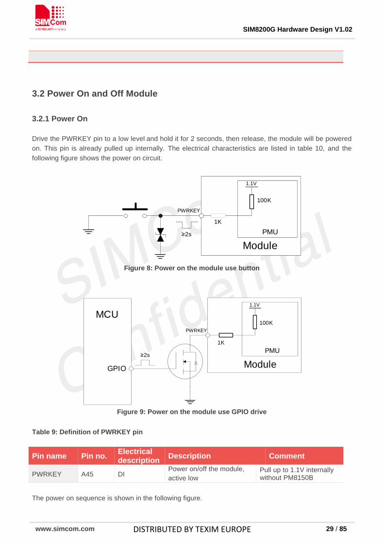
Table 9: Definition of PWRKEY pin ............................................................................................................. 29
Table 10: Power on timing and electronic characteristic ............................................................................. 30
Table 11: Power off timing and electronic characteristic .............................................................................. 31
Table 12: Definition of RESIN_N pin ........................................................................................................... 32
Table 13: RESET electronic characteristics ................................................................................................ 32
Table 14: Output power management summary ......................................................................................... 33
Table 15: Definition of USB interface .......................................................................................................... 35
Table 16: Recommended CC detector list................................................................................................... 36
Table 17: Recommended SS USB switch list .............................................................................................. 36
Table 18: Recommended OTG 5V DC-DC and USB interface TVS list ...................................................... 36
Table 19: Definition of PCIe interface .......................................................................................................... 38
Table 20: Definition of SDIO interface ......................................................................................................... 39
Table 21: Recommended TVS and SD card socket list ............................................................................... 40
Table 22: Definition of RGMII interface ....................................................................................................... 41
Table 23: (U)SIM electronic characteristics in 1.8V mode ((U)SIM_PWR=1.8V) ........................................ 42
Table 24: (U)SIM electronic characteristics 3.0V mode ((U)SIM_PWR=3.0V) ............................................ 42
Table 25: Definition of (U)SIM interface ...................................................................................................... 43
Table 26: Recommended TVS and (U)SIM socket list ................................................................................ 44
Table 27: I2S format .................................................................................................................................... 44
Table 28: I2S timing parameters ................................................................................................................. 45
Table 29: The PCM interface is multiplexing with I2S interface ................................................................... 46
Table 30: Definition of I2C interface ............................................................................................................ 47
Table 31: Definition of UART interface ........................................................................................................ 49
Table 32: Definition of SPI interface ............................................................................................................ 50
Table 33: Definition of ADC interface .......................................................................................................... 50
Table 34: ADC performance parameters ..................................................................................................... 50
Table 35: Definition of WLAN/BT interface .................................................................................................. 51
Table 36: Definition of PM8150B interface .................................................................................................. 53
Table 37: GPIO list ...................................................................................................................................... 54
Table 38: Definition of NET_STATUS pin .................................................................................................... 55
Table 39: NET_STATUS pin status ............................................................................................................. 55
Table 40: Definition of W_DISABLE pin ...................................................................................................... 56
DISTRIBUTED BY TEXIM EUROPE

SIM8200G Hardware Design V1.02
www.simcom.com 7 / 85
Table 41: W_DISABLE pin status ............................................................................................................... 56
Table 42: Definition of antenna control interface through GPIOs ................................................................ 57
Table 43: Antenna port definitions ............................................................................................................... 58
Table 44: SIM8200G operating frequencies ................................................................................................ 59
Table 45: NR band ...................................................................................................................................... 60
Table 46: GNSS frequency ......................................................................................................................... 60
Table 47: 3G/4G/5G/GNSS antennas ......................................................................................................... 61
Table 48: GNSS antenna (for dedicated GNSS antenna only)* .................................................................. 61
Table 49: Absolute maximum ratings .......................................................................................................... 63
Table 50: VBAT recommended operating ratings ........................................................................................ 63
Table 51: 1.8V digital I/O characteristics ..................................................................................................... 64
Table 52: Operating temperature ................................................................................................................ 64
Table 53: Operating mode definition ........................................................................................................... 64
Table 54: Current consumption on VBAT pins (VBAT1=3.8V) ..................................................................... 66
Table 55: Conducted output power ............................................................................................................. 68
Table 56: The ESD performance measurement table (temperature: 25℃, humidity: 45%) ......................... 69
Table 57: Label description of module information ...................................................................................... 72
Table 58: MSL ratings summary .................................................................................................................. 76
Table 59: Baking requirements ................................................................................................................... 76
Table 60: Tray size ...................................................................................................................................... 78
Table 61: Small carton size ......................................................................................................................... 78
Table 62: Big carton size ............................................................................................................................. 79
Table 63: Coding schemes and maximum net data rates over air interface ................................................ 80
Table 64: Related documents ..................................................................................................................... 82
Table 65: Terms and abbreviations ............................................................................................................. 83
Table 66: Safety caution.............................................................................................................................. 85
DISTRIBUTED BY TEXIM EUROPE

SIM8200G Hardware Design V1.02
www.simcom.com 8 / 85
Figure Index
Figure 1: SIM8200G module block diagram ................................................................................................ 11
Figure 2: Pin assignment ............................................................................................................................ 14
Figure 3: Dimensions of SIM8200G (unit: mm) ........................................................................................... 24
Figure 4:VBAT voltage drop at maximum power radio transmission ........................................................... 26
Figure 5: Power supply reference circuit ..................................................................................................... 26
Figure 6: Linear regulator reference circuit ................................................................................................. 28
Figure 7: Switching mode power supply reference circuit ........................................................................... 28
Figure 8: Power on the module use button ................................................................................................. 29
Figure 9: Power on the module use GPIO drive ......................................................................................... 29
Figure 10: Power on sequence ................................................................................................................... 30
Figure 11: Power off sequence ................................................................................................................... 31
Figure 12: Reset the module use GPIO drive ............................................................................................. 32
Figure 13: Reset the module use button ..................................................................................................... 32
Figure 14: The reset timing sequence of the module .................................................................................. 33
Figure 15: Type-C USB reference circuit with PM8150B ............................................................................ 34
Figure 16: Type-C USB reference circuit with CC detector ......................................................................... 34
Figure 17: USB3.1 reference circuit ............................................................................................................ 35
Figure 18: PCIe interface reference circuit(RC) .......................................................................................... 37
Figure 19: PCIe interface reference circuit (EP) ......................................................................................... 37
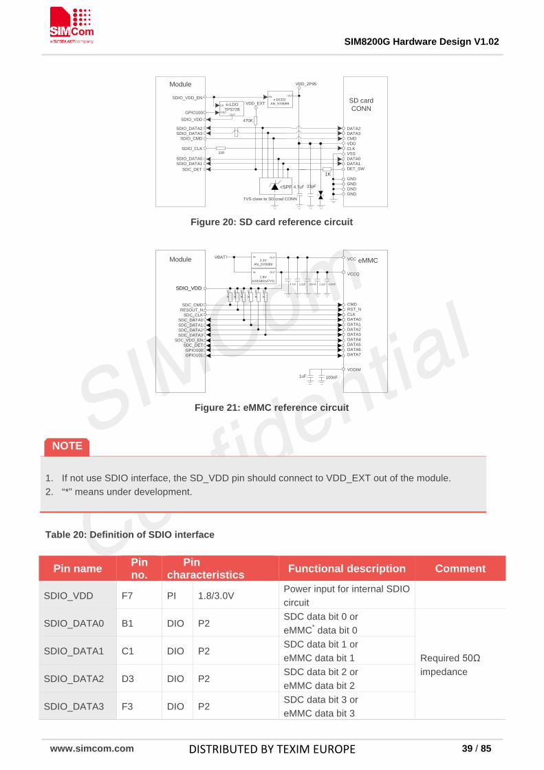
Figure 20: SD card reference circuit ........................................................................................................... 39
Figure 21: eMMC reference circuit .............................................................................................................. 39
Figure 22: RGMII to RJ45 diagram circuit ................................................................................................... 41
Figure 23: (U)SIM interface reference circuit .............................................................................................. 43
Figure 24: I2S timing ................................................................................................................................... 45
Figure 25: Audio codec reference circuit ..................................................................................................... 46
Figure 26: I2C reference circuit ................................................................................................................... 47
Figure 27: UART level conversion circuit .................................................................................................... 48
Figure 28: UART TX level conversion circuit ............................................................................................... 48
Figure 29: UART RX level conversion circuit .............................................................................................. 48
Figure 30: SPI reference circuit .................................................................................................................. 50
Figure 31: SIM8200G and W80 connect circuit .......................................................................................... 51
Figure 32: PM8150B interface diagram circuit ............................................................................................ 53
Figure 33: NET_STATUS reference circuit ................................................................................................. 55
Figure 34: W_DISABLE pin reference circuit .............................................................................................. 56
Figure 35: Top and bottom view of SIM8200G ............................................................................................ 71
Figure 36: Label description of module ....................................................................................................... 71
Figure 37: Recommended PCB footprint .................................................................................................... 73
Figure 38: Recommended SMT stencil ....................................................................................................... 74
Figure 39: Recommended SMT reflow profile ............................................................................................. 75
Figure 40: Packaging process .................................................................................................................... 77
DISTRIBUTED BY TEXIM EUROPE

SIM8200G Hardware Design V1.02
www.simcom.com 9 / 85
Figure 41: Module tray drawing .................................................................................................................. 77
Figure 42: Small carton drawing ................................................................................................................. 78
Figure 43: Big carton drawing ..................................................................................................................... 79
DISTRIBUTED BY TEXIM EUROPE
SIM8200G Hardware Design V1.02
www.simcom.com 10 / 85
1. Introduction This document describes the electronic specifications, RF specifications, interfaces, mechanical characteristics and test results of the SIM8200G module. With the help of this document,customers can quickly understand SIM8200G module. Associated with other software application notes and user guides, customers can use SIM8200G to design and develop mobile and laptop applications easily.
1.1 Product Outline
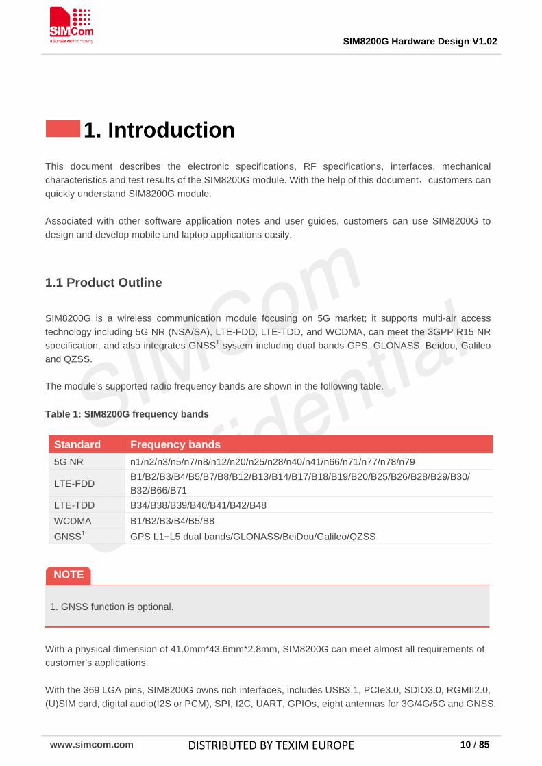
SIM8200G is a wireless communication module focusing on 5G market; it supports multi-air access technology including 5G NR (NSA/SA), LTE-FDD, LTE-TDD, and WCDMA, can meet the 3GPP R15 NR specification, and also integrates GNSS1 system including dual bands GPS, GLONASS, Beidou, Galileo and QZSS. The module’s supported radio frequency bands are shown in the following table. Table 1: SIM8200G frequency bands
Standard Frequency bands 5G NR n1/n2/n3/n5/n7/n8/n12/n20/n25/n28/n40/n41/n66/n71/n77/n78/n79
LTE-FDD B1/B2/B3/B4/B5/B7/B8/B12/B13/B14/B17/B18/B19/B20/B25/B26/B28/B29/B30/ B32/B66/B71
LTE-TDD B34/B38/B39/B40/B41/B42/B48 WCDMA B1/B2/B3/B4/B5/B8 GNSS1 GPS L1+L5 dual bands/GLONASS/BeiDou/Galileo/QZSS
1. GNSS function is optional.
With a physical dimension of 41.0mm*43.6mm*2.8mm, SIM8200G can meet almost all requirements of customer’s applications. With the 369 LGA pins, SIM8200G owns rich interfaces, includes USB3.1, PCIe3.0, SDIO3.0, RGMII2.0, (U)SIM card, digital audio(I2S or PCM), SPI, I2C, UART, GPIOs, eight antennas for 3G/4G/5G and GNSS.
NOTE
DISTRIBUTED BY TEXIM EUROPE

SIM8200G Hardware Design V1.02
www.simcom.com 11 / 85
With all these interfaces, SIM8200G can also be utilized in the handheld terminal, machine-to-machine laptop application and especially the 5G CPE.
1.2 Hardware Block Diagram
The block diagram of SIM8200G is shown in the following figure.
PMIC
TX/RX Blocks
Baseband
Transcevier4G+5G(sub-6 GHz) RF
NANDLPDDR4XSDRAM
5G_MAIN 5G_DIV15G_DIV2 5G_DIV3LTE_MAIN LTE_DV1LTE_DV2 ANT_GNSS
APTVBAT_RF
38.4MTCXO
VBAT_BB
PWRKEY
ADCs
RESET_N
VDD_EXT USB3.1 (U)SIMPCIe I2CUART GPIOs SDIO
STATUS
SPI
Tx Rx GRFCs
QLINK Control
RFFEs
RGMII
I2S/PCM
PMIBT/WIFI(W80)
Figure 1: SIM8200G module block diagram
1.3 Feature Overview
Table 2: Key features
Feature Implementation Application processor Arm Cortex-A7 up to 1.5 GHz Memory RAM 4Gb 16-bit LPDDR4X at 1.8 GHz Memory ROM 4Gb 8-bit NAND
Power supply VBAT:3.3V~4.4V Typical: 3.8V
Power consumption < 3mA @sleep mode(VBAT=3.8V)
Transmit power Power Class 3 for WCDMA/LTE/5G NR
Data transmission throughput
4Gbps (DL)/500Mbps(UL) for NR 2Gbps (DL)/200Mbps(UL) for LTE 42 Mbps(DL)/5.76Mbps(UL) for HSPA+
Antenna Eight antennas for 3G/4G/5G and GNSS
GNSS(optional) GNSS engine: GPS L1+L5/GLONASS/BeiDou/Galileo/QZSS Protocol: NMEA
SMS MT, MO, CB, Text and PDU mode SMS storage: (U)SIM card or ME(default)
DISTRIBUTED BY TEXIM EUROPE

SIM8200G Hardware Design V1.02
www.simcom.com 12 / 85
Transmission of SMS alternatively over CS or PS.
(U)SIM interface Support identity card: 1.8V/ 3.0V Include (U)SIM1 and (U)SIM2 interfaces Support Dual SIM single standby
(U)SIM application toolkit Support SAT class 3 Support USAT
Phonebook management Support phonebook types: DC,MC,RC,SM,ME,FD,ON,LD,EN
Digital audio interface
One I2S interface with dedicated main-clock for primary digital audio, the I2S also can be configured as PCM MCLK frequency: 12.288MHz (default) WCDMA AMR-NB VoLTE AMR-WB Echo cancellation Noise suppression
PCIe interface Two lane PCIe interfaces, support PCIe Gen 3 (Gen 1/2 compatible) High communication data rate which up to 8Gbps per lane.
WLAN/BT interface Support W80 interface, which support 802.11ax with 1.775Gbps
RGMII interface Integrated RGMII MAC for Ethernet Data rate up to 1000Mbps
PMI interface Support PM8150B interface, which support USB Type-C and QC4.0*
UART interface Support up to three UART Data rate up to 4 Mbps
I2C interface Support up to two I2C, meet I2C specification, version 5.0 Data rate up to 400 Kbps
SPI interface Only support master mode Data rate up to 50Mbps
SDIO interface Support 4bit SD card or 8bit eMMC*, meet SDIO3.0 specification 1.8V or 3.0V dual-voltage operation for SD card Data rate up to 100Mbps
USB interface
USB3.1 Gen2 or USB2.0 USB3.1: super speed, with data rate which up to 10Gbps USB2.0: high speed interface, support USB operations at low-speed and full-speed, which refer to USB1.0 and USB1.1
Firmware upgrade Firmware upgrade over USB interface
Physical characteristics Size: 41mm*43.6mm*2.8mm Weight: 11.17g
Temperature range Normal operation temperature: -30°C to +70°C 3GPP compliant Extended operation temperature: -40°C to +85°C2 Storage temperature: -40°C to +90°C
1. “*” means under development. 2. Module is able to establish and maintain voice, data transmission, SMS and emergency call, etc. The performance may deviate slightly from the 3GPP specifications and will meet 3GPP specifications
NOTE
DISTRIBUTED BY TEXIM EUROPE

SIM8200G Hardware Design V1.02
www.simcom.com 13 / 85
again when the temperature returns to normal operating temperature levels.
DISTRIBUTED BY TEXIM EUROPE

SIM8200G Hardware Design V1.02
www.simcom.com 14 / 85
2. Package Information
2.1 Pin Assignment Overview All functions of the SIM8200G will be provided through 369 LGA pins that will be connected to the customer’s platform. The following figure is a high-level view of the pin assignment of the module.
GND GND GND GNDGND GNDGND GND GND GND GND GND GND EMAC_OUT
GND GNDGND GNDANT_CTRL1
WL_TX_EN
GND GND GND GNDGND GNDGND GND GND GND GND RFU RFU GNDRESOUT_N
GND GND GND
ANT7 GND GND GNDANT4 GNDANT2 GND GND GND GND ANT1 GNDRFFE0_CLK
RFFE0_DATA
COEX_UART_RXD
GND ANT5 GNDANT_CTRL0
GNDCOEX_UART_TXD
GND
GND GND GND GNDGND GNDGND GND GND GND GND GND GND GND GND GND GND
(U)IM2_DE
T
WL_PA_MUTING
WL_EN
VBAT_RF
VBAT_RF
VBAT_RF
S2E_1P224
RFU
PON_1
VBAT_BB
GND
GND
RFU
RFU
RFU
RFU
SPMI_DATA
FAULT_N GND
RGMII_TX_
1
RGMII_TX
_3GND
RGMII_RX_0
RGMII_RX_2
RGMII_RX_CLK
RGMII_TX_CLK
PCIe_RX0
_P
PCIe_RX1
_P
PCIe_REFCLK_P
USB_SS_RX_P
GND GNDPCIe_TX1_M
PCIe_TX0_M
GNDUSB_SS_TX_M
CHG_SYS_OK
L10E_3P1
RGMII_INT
_NGND
RGMII_RST_N
PCIe_WAKE
GND GND GND GNDPCIe_RST
PCIe_CLKREQ
GNDUSB_VBUS
GND GNDUSB_SS_SW
USB_ID
SPMI_CLK
PWRKEY
RESIN_N
RGMII_TX_
2
RGMII_TX_
0GNDGND
RGMII_RX_3
RGMII_RX_1
RGMII_TX_CTL
PCIe_RX0_M
PCIe_RX1_M
PCIe_REFCLK_M
USB_SS_RX_M
GND GNDPCIe_TX1
_P
PCIe_TX0
_PGND
USB_SS_TX_P
USB_HS_D
M
USB_HS_D
P
VIO_OUT GND
RGMII_3P3_EN
GNDGND GNDRGMII_PWR_EN
RGMII_MD_CLK
RGMII_PWR
_IN
RGMII_MD_IO
GND SPI_CLK
SPI_CS_
N
SPI_MISO
SPI_MOSI
USB_BOOT
OTG_EN
(U)IM2_DA
TA
WL_LAA_
RX
WL_TO_SDX_CTI
VBAT_RF
VBAT_RF
GND
S4E_1P904
GND
VBAT_RF
GND
GND
GND
GND
GND
GND
(U)IM1_DE
T
(U)IM2_CL
K
WL_SW_CT
RL
SDX_TO_WL_CTI
GND
GND
RFU
S3E_0P824
GND
VBAT_BB
VBAT_RF
RFU
GND
GND
RFU
RFU
GND
(U)IM2_VD
D
(U)IM1_CL
K
WL_LAA_AS_EN
BT_EN
WL_LAA_TX_ EN
RFU
GND
GND
GND
GND
GND
RFU
RFU
GND
RFU
GND
GND
ANT3
SLEEP_CL
K
(U)IM2_RS
T
(U)IM1_DA
TA
(U)IM1_RS
T
(U)IM1_VD
D
GND
PMX55_GPIO4
CDC_INT_N
I2C2_SDA
I2C2_SCL
BT_UART_RXD
CDC_RST
_N
ACD0
ADC1
GND
BT_UART_TXD
I2C1_SDA
I2C1_SCL
GPIO101
SDIO_VDD_EN
SDIO_VD
D
GND
GND
VDD_EXT
UART1_DCD
UART1_RI
BT_UART_RTS
STATUS
SLEEP_IN
NET_MOD
E
UART1_DT
R
BT_UART_CTS
DBG_UART_TXD
DBG_UART_RXD
GND
SDIO_CM
D
SDIO_CLK
GND
GND
GND
GND
UART2_CT
S
UART2_RT
S
I2S_WS
AP_STATUS
WAKEUP_OUT
UART1_RX
D
UART1_TX
D
I2S_CLK
WL_I2S_DIN
WL_I2S_DO
UT
GPIO100
SDIO_DAT
A3
SDIO_DAT
A2
GND
GND
ANT0
GND
W_DISABLE
UART2_TX
D
I2S_DIN
NET_STAT
US
UART1_RT
S
UART1_CT
S
UART2_RX
D
I2S_DOUT
I2S_MCLK
WL_I2S_CL
K
WL_I2S_WS
SDIO_DET
GND
GND
GND
GND
SDIO_DAT
A1
SDIO_DAT
A0
BA51
AY48
AW45
BA1
AW7
AY4
C45
B48
A51
RFU
C7
B4
A1
GND
GND
USB 2.0/3.1
PCIE
RGMII
USIM UART/SPI/I2CWIFI/BT Control
SD CARD
PMI
ADC
ANT
RF Related
I2S/PCM
Other
RFU
POWER
RGMII_RX_CTL
ANT6
System
SIM8200G
157911131517192123252729313335373941434547
A
B
C
E
G
J
L
N
R
U
W
AA
AC
AE
AG
AL
AN
AR
AU
AW
AJ
AY
51
D49
F49
K49
H49
M49
P49
T49
V49
Y49
AB49
AD49
AF49
AH49
AK49
AM49
AP49
AT49
AV49
BA
B51
C51
E51
G51
J51
L51
N51
R51
U51
W51
AA51
AC51
AE51
AG51
AL51
AN51
AR51
AU51
AW51
AJ51
AY51
GND GND GND GND GND GND GND
GND GND GND GND GND GND GND GND
GND GND GND GND GND GND GND GND
GND GND GND GND GND GND GND GND
GND GND GND GND GND GND GND GND
GND GND GND GND GND GND GND GND
GND GND GND GND GND GND GND GND
A
B
C
E
G
J
L
N
R
U
W
AA
AC
AE
AG
AL
AN
AR
AU
AW
AJ
AY
BA
15791113151719212325272931333537394143454751
E47
G47
J47
L47
N47
R47
U47
W47
AA47
AC47
AE47
AG47
AL47
AN47
AR47
AU47
AJ47
F45
K45
H45
M45
P45
T45
V45
Y45
AB45
AD45
AF45
AH45
AK45
AM45
AP45
AT45
F7
K7
H7
M7
P7
T7
V7
Y7
AB7
AD7
AF7
AH7
AK7
AM7
AP7
AT7
E5
G5
J5
L5
N5
R5
U5
W5
AA5
AC5
AE5
AG5
AL5
AN5
AR5
AU5
AJ5
D3
F3
K3
H3
M3
P3
T3
V3
Y3
AB3
AD3
AH3
AK3
AM3
AP3
AT3
AV3
AF3
B1
C1
E1
G1
J1
L1
N1
R1
U1
W1
AA1
AC1
AE1
AG1
AL1
AN1
AR1
AU1
AW1
AJ1
AY1
A47 A45 A43 A41 A39 A37 A35 A33 A31 A29 A27 A25 A23 A21 A19 A17 A15 A13 A11 A9 A7 A5
B46 B44 B42 B40 B38 B36 B34 B32 B30 B28 B26 B24 B22 B20 B18 B16 B14 B12 B10 B8 B6
C43 C41 C39 C37 C35 C33 C31 C29 C27 C25 C23 C21 C19 C17 C15 C13 C11 C9
D42 D40 D38 D36 D34 D32 D30 D28 D26 D24 D22 D20 D18 D16 D14 D12 D10
AV42 AV40 AV38 AV36 AV34 AV32 AV30 AV28 AV26 AV24 AV22 AV20 AV18 AV16 AV14 AV12 AV10
AW43 AW41 AW39 AW37 AW35 AW33 AW31 AW29 AW27 AW25 AW23 AW21 AW19 AW17 AW15 AW13 AW11 AW9
AY46 AY44 AY42 AY40 AY38 AY36 AY34 AY32 AY30 AY28 AY26 AY24 AY22 AY20 AY18 AY16 AY14 AY12 AY10 AY8 AY6
BA47 BA45 BA43 BA41 BA39 BA37 BA35 BA33 BA31 BA29 BA27 BA25 BA23 BA21 BA19 BA17 BA15 BA13 BA11 BA9 BA7 BA5
AM39 AM35 AM31 AM27 AM24 AM21 AM17 AM13
AH39 AH35 AH31 AH27 AH24 AH21 AH17 AH13
AE39 AE35 AE31 AE27 AE24 AE21 AE17 AE13
AA39 AA35 AA31 AA27 AA24 AA21 AA17 AA13
U39 U35 U31 U27 U24 U21 U17 U13
P39 P35 P31 P27 P24 P21 P17 P13
K39 K35 K31 K27 K24 K21 K17 K13
D9
VBAT_BB
Figure 2: Pin assignment
DISTRIBUTED BY TEXIM EUROPE

SIM8200G Hardware Design V1.02
www.simcom.com 15 / 85
2.2 Pin Description
Table 3: IO parameters definition
Pin type Description PI Power Input PO Power Output AI Analog Input AIO Analog Input /Output DIO Bidirectional Digital Input /Output DI Digital Input DO Digital Output PU Pull Up PD Pull Down
Table 4: DC parameters definition Voltage domain Parameter Min Typ Max
P2
VDD_P2=1.8V VOH High level output 1.4V - - VOL Low level output 0V - 0.45V VIH High level input 1.27V - 2V VIL Low level input 0V - 0.58V
Rp Pull up/down resistor
10K ohm - 100K ohm
VDD_P2=3.0V VOH High level output 2.25V - 3.0V VOL Low level output 0V - 0.375V VIH High level input 1.84V - 3.25V VIL Low level input 0V - 0.75V
Rp Pull up/down resistor
10K ohm - 100K ohm
P3
VDD_P3=1.8V VOH High level output 1.35V - 1.8V VOL Low level output 0V - 0.45V VIH High level input 1.26V 2.1V VIL Low level input 0V - 0.6V
Rp Pull up/down resistor
20K ohm - 60K ohm
P4/P5 VDD_P4/P5=1.8V
DISTRIBUTED BY TEXIM EUROPE

SIM8200G Hardware Design V1.02
www.simcom.com 16 / 85
Table 5: Pin description
Pin name Pin no.
Electrical description Description Comment
Power supply
VBAT_BB V45, V49, U47
PI VMAX=4.4V VTYP =3.8V VMIN=3.3V
Input power supply for module’s BB part
VBAT_RF
Y49, AC47,AA47,W47, AD45,AB45,Y45
PI VMAX=4.4V VTYP =3.8V VMIN=3.3V
Input power supply for module’s RF part
VDD_EXT AL5 PO VTYP =1.8V Output power supply for external IO pull up circuits
S2E_1P224 M45 PO VTYP =1.28V Output power supply for W80 only
S3E_0P824 P49 PO VTYP =0.88V Output power supply for W80 only
S4E_1P904 N47 PO VTYP=1.88V Output power supply for W80 only
L10E_3P1 C41 PO VTYP=3.08V Output power supply for PM8150B USB PD-PHY and USB switch
VIO_OUT D42 PO VTYP=1.8V Output power supply for PM8150B IO circuit only
VOH High level output 1.44V - 1.8V VOL Low level output 0V - 0.4V VIH High level input 1.26V - 2.1V VIL Low level input 0V - 0.36V
Rp Pull up/down resistor
10K ohm - 100K ohm
VDD_P4/P5=3.0V VOH High level output 2.4V - 3.0V VOL Low level output 0V - 0.4V VIH High level input 2.1V - 3.05V VIL Low level input 0V - 0.6V
Rp Pull up/down resistor
10K ohm - 100K ohm
P8 VDD_P8=1.8/2.5V
Rp Pull up/down resistor
20K ohm - 50K ohm
DISTRIBUTED BY TEXIM EUROPE

SIM8200G Hardware Design V1.02
www.simcom.com 17 / 85
GND
A7,B8,A11,B12,C15,A15,B16,C17,C19,D22,D24,D26,C27,A27,B28,D28,C31,C33,C35,C37,D40,A41,B42,J5,AD7,AJ1,AK3,AM3,AN1,AN5,AP3,AR1,AR5,AT3,AT7,AU1,AU5,AV3,AW1,R47,T49,U51,W51,AA51,AB49,AD49,AE47,AF45,AH45,AG47,AJ47,AL47,AN47,AR47,AU47,AV49,AW51,AV10,AV12,AV14,AV16,AV18,AV20,AV22,AV24,AV26,AV28,AV30,AV32,AV34,AV36,AV38,AV40,AV42,AW9,AW11,AW13,AW15,AW23,AW25,AW27,AW29,AW31,AW33,AW35,AW37,AW39,AW41,AW43,AY6,AY8,AY12,AY18,AY20,AY22,AY24,AY26,AY28,AY30,AY32,AY34,AY36,AY38,AY40,AY42,AY44,AY46,BA5,BA17,BA21,BA23,BA27,BA29,BA31,BA35,BA39,BA43,BA45,AM13,AM17,AM21,AM24,AM27,AM31,AM35,AM39,AH13,AH17,AH21,AH24,AH27,AH31,AH35,AH39,AE13,AE17,AE21,AE24,AE27,AE31,AE35,AE39,AA13,AA17,AA21,AA24,AA27,AA31,AA35,AA39,U13,U17,U21,U24,U27,U31,U35,U39,P13,P17,P21,P24,P27,P31,P35,P39,K13,K17,K21,K24,K27,K31,K35,K39,A1,B4,C7,A51,B48,C45,BA1,AY4,AW7,BA51,AY48,AW45
Ground
System control
PWRKEY2 A45 DI 1.1V Power on/off the module, active low
Pull up to 1.1V internally without PM8150B
PON_1 T45 DI 1.8V Power on the module, active high
RESIN_N A43 DI P3 Reset the module, active low
Status indicator
STATUS AJ5 DO P3 Indicate operation status of the module
AP_STATUS AH3 DI P3 Indicate operation status of the AP
NET_MODE* AE5 DO P3 Indicate network registration mode of the module
NET_STATUS AE1 DO P3 Indicate network activity status of the module
USB interface USB_VBUS C9 AI USB VBUS detection Not support charge
USB_HS_DP B6 AIO Differential USB bi-directional data plus
Required 90Ω differential impedance Compliant with USB 2.0 standard specifications
USB_HS_DM A5 AIO Differential USB bi-directional data minus
USB_SS_TX_P A13 AO USB3.1 super-speed transmit data plus
Required 90Ω differential Impedance Compliant with USB
USB_SS_TX_M B14 AO USB3.1 super-speed transmit data minus
DISTRIBUTED BY TEXIM EUROPE

SIM8200G Hardware Design V1.02
www.simcom.com 18 / 85
USB_SS_ RX_P B10 AI USB3.1 super-speed receive data plus
3.1 standard specifications
USB_SS_RX_M A9 AI USB3.1 super-speed receive data minus
USB_ID* C11 DI P3 USB ID If unused, please keep open
OTG_EN* D10 DO P3 USB OTG power supply DC-DC enable signal
USB_SS_SW C13 DO P3 USB Type-C switch control signal
(U)SIM interface (U)SIM1_VDD B51 PO Power supply for (U)SIM1 card
1.8/3.0V voltage domain, (U)SIM interface should be protected against ESD. If unused, please keep open
(U)SIM1_DATA E51 DIO P4
(U)SIM1 card data signal, which has been pulled up to (U)SIM1_VDD by a 20K resistor internally
(U)SIM1_CLK D49 DO P4 (U)SIM1 clock signal
(U)SIM1_RST C51 DO P4 (U)SIM1 reset signal
(U)SIM1_DET E47 DI P3
(U)SIM1 card detect signal, which need pulled up to VDD_EXT by a 470K resistor externally
(U)SIM2_VDD F49 PO Power supply for (U)SIM2 card
(U)SIM2_DATA G47 DIO P5 (U)SIM1 card data, which has been pulled up to (U)SIM1_VDD by a 20K resistor internally
(U)SIM2_CLK H49 DO P5 (U)SIM2 clock signal
(U)SIM2_RST G51 DO P5 (U)SIM2 reset signal
(U)SIM2_DET F45 DI P3 (U)SIM1 card detect, which need pulled up to VDD_EXT by a 470KR resistor externally
SPI interface SPI_CS_N D18 DO P3 SPI chip select SPI_CLK D20 DO P3 SPI clock SPI_MOSI D14 DO P3 Master output slaver input SPI_MISO D16 DI P3 Master input slaver output
UART1 interface UART1_CTS AA1 DO P3 Clear to send
Default use for AT command
UART1_RTS AC1 DI P3 Request to send UART1_TXD AB3 DO P3 Transmit data UART1_RXD AD3 DI P3 Receive data UART1_DCD W5 DO P3 Carrier detect
UART1_RI AA5 DO P3 Ring indicator
DISTRIBUTED BY TEXIM EUROPE

SIM8200G Hardware Design V1.02
www.simcom.com 19 / 85
UART1_DTR AC5 DI P3 Data terminal ready
UART2 interface UART2_CTS V3 DO P3 Clear to send
UART2_RTS Y3 DI P3 Request to send UART2_TXD U1 DO P3 Transmit data UART2_RXD W1 DI P3 Receive data
BT UART interface BT_UART_CTS R5 DO P3 Clear to send
Default use for BT BT_UART_RTS U5 DI P3 Request to send BT_UART_TXD T7 DO P3 Transmit data BT_UART_RXD V7 DI P3 Receive data
Debug UART interface DBG_UART_RXD
L5 DI P3 Receive data Used for debug only
DBG_UART_TXD
N5 DO P3 Transmit data
I2C interface3
I2C1_SCL M7 OD P3 I2C1 clock signal I2C1 default use for codec Pull up to VDD_EXT externally
I2C1_SDA P7 OD P3 I2C1 data signal
I2C2_SCL AB7 OD P3 I2C2 clock signal I2C2 default use for sensor Pull up to VDD_EXT externally
I2C2_SDA Y7 OD P3 I2C2 data signal
WLAN I2S interface WL_ I2S_DOUT K3 DO P3 WLAN I2S data output
Default use for WLAN
WL_ I2S_DIN M3 DI P3 WLAN I2S data input WL_I2S_CLK J1 DO P3 WLAN I2S bit clock WL_ I2S_WS G1 DO P3 WLAN I2S word select
I2S(PCM) interface I2S_DOUT/ PCM_DOUT
N1 DO P3 I2S/PCM data output Default is I2S interface, can be configured as PCM interface by software, If unused, please keep open
I2S_DIN/ PCM_DIN
R1 DI P3 I2S/PCM data input
I2S_CLK/ PCM_CLK
P3 DO P3 I2S/PCM clock output
I2S_WS/ PCM_SYNC
T3 DIO P3 I2S word select/ PCM synchronous signal
I2S_MCLK L1 DO P3 I2S master clock output
ADC interface
ADC0 AH7 AI Analog to digital converter input0
DISTRIBUTED BY TEXIM EUROPE

SIM8200G Hardware Design V1.02
www.simcom.com 20 / 85
ADC1 AF7 AI Analog to digital converter input1
RGMII interface4
RGMII_MD_IO D30 DIO P8 RGMII management data
Required 50Ω impedance
RGMII_MD_CLK
D34 DO P8 RGMII management data clock
RGMII _RX_CTL
A35 DI P8 RGMII receive control
RGMII _RX_CLK
B36 DI P8 RGMII receive clock
RGMII_RX_0 B40 DI P8 RGMII receive data bit 0 RGMII_RX_1 A37 DI P8 RGMII receive data bit 1 RGMII_RX_2 B38 DI P8 RGMII receive data bit 2 RGMII_RX_3 A39 DI P8 RGMII receive data bit 3 RGMII _TX_CTL
A33 DO P8 RGMII transmit control
RGMII _TX_CLK
B34 DO P8 RGMII transmit clock
RGMII_TX_0 A31 DO P8 RGMII transmit data bit 0 RGMII_TX_1 B30 DO P8 RGMII transmit data bit 1 RGMII_TX_2 A29 DO P8 RGMII transmit data bit 2 RGMII_TX_3 B32 DO P8 RGMII transmit data bit 3 RGMII_INT_N C39 DI P3 Interrupt input from RGMII PHY RGMII_RST_N C29 DO P3 Reset output to RGMII PHY
RGMII_PWR_EN
D36 DO P3 Used to enable external LDO to supply 1.8V power to RGMII_PWR_IN
RGMII_PWR_IN D32 PI 1.8V Power supply input for internal RGMII circuit
RGMII_3P3_EN D38 DO P3 Used to enable external DC-DC/LDO to supply 3.3V power to RGMII PHY
PCIe interface5
PCIe_REFCLK_P
B22 AIO PCIe reference clock plus
Required 90Ω differential impedance
PCIe_REFCLK_M
A21 AIO PCIe reference clock minus
PCIe_TX0_M B18 AO PCIe transmit0 minus PCIe_TX0_P A17 AO PCIe transmit0 plus PCIe_TX1_M* B20 AO PCIe transmit1 minus PCIe_TX1_P* A19 AO PCIe transmit1 plus PCIe_RX0_M A25 AI PCIe receive0 minus PCIe_RX0_P B26 AI PCIe receive0 plus PCIe_RX1_M* A23 AI PCIe receive1 minus
DISTRIBUTED BY TEXIM EUROPE

SIM8200G Hardware Design V1.02
www.simcom.com 21 / 85
PCIe_RX1_P* B24 AI PCIe receive1 plus
PCIe_CLKREQ C21 DI P3 PCIe clock request CLKREQ and WAKE need pull up to VDD_EXT externally, Default as RC mode
PCIe_WAKE C25 DI P3 PCIe wake-up
PCIe_RST C23 DO P3 PCIe reset
W80 interface WL_SW_CTRL K49 DO P3 W80 switch control SDX_TO_WL_CTI
M49 DO P3 W80 GPIO
WL_TO_SDX_CTI
L47 DI P3 W80 GPIO
BT_EN N51 DO P3 W80 BT enable SLEEP_CLK J51 DO Sleep clock output for W80 only WL_EN K45 DO P3 WLAN enable
WL_LAA_RX J47 DI P3 WLAN XFEM control for LAA receiver
W80 RF coexistence signals
WL_PA_MUTING
H45 DO P3 WLAN XFEM control for PA mute
WL_LAA_AS_EN
L51 DO P3 WLAN LAA AS enable
WL_LAA_TX_EN
R51 DO P3 WLAN XFEM control for LAA enable
COEX_UART_TXD
BA7 DO P3 LTE&WLAN coexistence data transmit
COEX_UART_RXD
BA9 DI P3 LTE&WLAN coexistence data receive
WL_TX_EN AY14 DI P3 WLAN XFEM control for WLAN TX enable
SDIO interface
SDIO_VDD F7 PI 1.8/3.0V Power input for internal SDIO circuit
SDIO_DATA0 B1 DIO P2 SDC data bit 0 or eMMC* data bit 0
Required 50Ω impedance
SDIO_DATA1 C1 DIO P2 SDC data bit 1 or eMMC data bit 1
SDIO_DATA2 D3 DIO P2 SDC data bit 2 or eMMC data bit 2
SDIO_DATA3 F3 DIO P2 SDC data bit 3 or eMMC data bit 3
SDIO_CMD G5 DIO P2 SDC command output
SDIO_CLK E5 DO P2 SDC clock output
SDIO_VDD_EN H7 DO P3 Enable the SD card power or eMMC data bit 4
If used as eMMC data signals,
DISTRIBUTED BY TEXIM EUROPE

SIM8200G Hardware Design V1.02
www.simcom.com 22 / 85
SDIO_DET E1 DI P3 SD card insertion detect or eMMC data bit 5
required 50Ω impedance, GPIO100 H3 DIO P3 eMMC data bit 6
GPIO101 K7 DIO P3 eMMC data bit 7
RESOUT_N* AW17 DO P3 eMMC RST_N If use this pin please confirm with SIMCom support teams
PM8150B interface
CHG_SYS_OK C43 DI When charger input is inserted PM8150B output signal to PMU
Used for PM8150B only
FAULT_N B44 DIO Used to send/receive the fault condition across all PMICs in the chipset
SPMI_CLK A47 DO SPMI communication bus clock signal Required 50Ω
impedance SPMI_DATA B46 DIO
SPMI communication bus data signal
Other interface EMAC_OUT* AY10 DO P3 1PPS time sync output
USB_BOOT D12 DI P3 Module will be forced into USB boot mode by connect this pin to VDD_EXT externally
W_DISABLE* AG1 DI P3 Flight mode control input active low
SLEEP_IN AG5 DI P3 Sleep mode control input WAKEUP_OUT AF3 DO P3 Module wake up the external AP
CDC_RST_N AK7 DO P3 Module reset the external CODEC active low
CDC_INT_N AM7 DI P3 External CODEC interrupt input active low
Antenna control interface6
RFFE0_CLK BA11 DO P3 Antenna tuner MIPI CLK RFFE0_DATA BA13 DIO P3 Antenna tuner MIPI DATA ANT_CTRL0 BA15 DO P3 Antenna tuner control0 ANT_CTRL1 AY16 DO P3 Antenna tuner control1
Antenna interface
ANT0 AL1 AIO
LTE low/middle/high BAND signal send and receive; n41 signal send and receive; n79 signal diversity receive
617MHz~960MHz 1710MHz~2690MHz 4400MHz~5000MHz
ANT1 BA25 AI LTE middle/high band signal diversity receive; n41&n77 signal diversity receive
1710MHz~2690MHz 3300MHz~4200MHz
DISTRIBUTED BY TEXIM EUROPE

SIM8200G Hardware Design V1.02
www.simcom.com 23 / 85
ANT2 BA41 AIO LTE low/middle/high band signal diversity receive; N79 signal send and receive
617MHz~960MHz 1710MHz~2690MHz 4400MHz~5000MHz
ANT3 AY51 AIO
LTE middle/high BAND signal diversity receive; n41 signal diversity receive; n77 signal send and receive
1710MHz~2690MHz 3300MHz~4200MHz
ANT4 BA33 AIO n41 signal send and receive; n77 signal diversity receive
2496MHz~2690MHz 3300MHz~4200MHz
ANT5 BA19 AIO n77 signal send and receive 3300MHz~4200MHz
ANT6 AY1 AI n79 signal diversity receive; GNSS signal receive ;
1166MHz~1229MHz 1565MHz~1610MHz 4400MHz~5000MHz
ANT7 BA47 AIO n79 signal send and receive 4400MHz~5000MHz
RFU interface
RFU
AP7,AW19,AW21,AT45,AP45,AM45,AK45,AG51,AU51,AR51,AN51,AJ51,AL51,AE51,AC51,BA37,AT49,AP49,AM49,AK49,AH49,AF49,P45,D9
Reserved for future use
1. “*” means under development. 2. PWRKEY will be pulled up to 1.8V internally if used PM8150B. 3. The I2C signals need pull up to VDD_EXT by 2.2K resistors out of the module. 4. If not use RGMII function, the RGMII_PWR_IN pin should connect to VDD_EXT out of the module. 5. If not use SDIO function, the SDIO_VDD pin should connect to VDD_EXT out of the module. 6. Please confirm with SIMCom for the details design about antenna control interface. 7. Only used to W80 and PM8150B pins don’t use as other circuits. 8. Unused and RFU pins should keep open. 9. Recommend ESD protect components out of the module for used interfaces. 10. The GPIO MAX voltage is 2.1V, if exceeded, may cause permanent damage to the module. 11. All GND pins should be connected to the customer’s main PCB.
NOTE
DISTRIBUTED BY TEXIM EUROPE

SIM8200G Hardware Design V1.02
www.simcom.com 24 / 85
2.3 Mechanical Dimensions
The following figure shows the mechanical dimensions of SIM8200G.
Figure 3: Dimensions of SIM8200G (unit: mm)
DISTRIBUTED BY TEXIM EUROPE

SIM8200G Hardware Design V1.02
www.simcom.com 25 / 85
3. Interface Application
3.1 Power Supply
The recommended power supply for SIM8200G is 3.8V and the voltage range is 3.3V to 4.4V. Please ensure that the input voltage is never lower than 3.3V, otherwise the module will be powered off automatically. The module has 3 BB power pins, 7 RF power pins and 10 power ground pins, to ensure the module works normally, all power and ground pins should be connected. Table 6: VBAT pins electronic characteristics Symbol Description Min. Typ. Max. Unit VBAT1 Module power supply voltage 3.3 3.8 4.4 V Ipeak
2 Peak current - - 2.5 A Isleep
2 Current in sleep mode - TBD - mA Ileakage
2 Current in power off mode - 80 - uA
1. The VBAT include VBAT_BB and VBAT_RF pins in this document. 2. Total current of the whole module.
3.1.1 Power Supply Design Guide When the module is transmitting at maximum power, the peak current can reach 2.5A, which results in voltage dropping on VBAT. To ensure that the voltage is not lower than required 3.3V, the capacity of the external power supply must be not less than 3A. The following figure shows the maximum voltage drop during maximum power radio transmission.
NOTE
DISTRIBUTED BY TEXIM EUROPE

SIM8200G Hardware Design V1.02
www.simcom.com 26 / 85
IVBAT
Ipeak
VBAT
VBAT>3.3V
3.5ms 1.5msVoltage Drop
Figure 4: VBAT voltage drop at maximum power radio transmission When the maximum voltage drops, make sure that the VBAT voltage is not less than 3.3V.External power supply can support more than 3A current to VBAT pins. The following figure shows the power reference circuit of VBAT.
GNDGND
C7100uF
AD45V49
U47
VBAT_BB V45 C6100nF
C833pF
C433pF
VBAT_BB
VBAT_BBVBAT_RF
VBAT_RFVBAT_RFVBAT_RFVBAT_RFVBAT_RFVBAT_RF
AC47AB45AA47Y49
Y45
W47
GNDGNDGNDGNDGND
D1
VBAT
C1220uF
5.1V
C3100nF
C2
C5220uF
100uF
GNDGNDGND
Module
AF45
R47
AD49
T49
AE47
AD49AB49AA51
W51U51
Figure 5: Power supply reference circuit Table 7: Definition of VBAT and GND pins
Pin name Pin no. Electrical description Description Comment
VBAT_BB V45, V49, U47
PI VMAX=4.4V VTYP =3.8V VMIN=3.3V
Input power supply for module’s BB part
VBAT_RF
Y49, AC47,AA47,W47, AD45,AB45,Y45
PI VMAX=4.4V VTYP =3.8V VMIN=3.3V
Input power supply for module’s RF part
GND
A7,B8,A11,B12,C15,A15,B16,C17,C19,D22,D24,D26,C27,A27,B28,D28,C31,C33,C35,C37,D40,A41,B42,J5,AD7,AJ1,AK3,AM3,AN1,AN5,AP3,AR1,AR5,AT3,AT7,AU1,AU5,AV3,AW1,R47,T49,U51,W51,AA51,AB49,AD49,AE47,AF45,AH45,
Ground
DISTRIBUTED BY TEXIM EUROPE

SIM8200G Hardware Design V1.02
www.simcom.com 27 / 85
AG47,AJ47,AL47,AN47,AR47,AU47,AV49,AW51,AV10,AV12,AV14,AV16,AV18,AV20,AV22,AV24,AV26,AV28,AV30,AV32,AV34,AV36,AV38,AV40,AV42,AW9,AW11,AW13,AW15,AW23,AW25,AW27,AW29,AW31,AW33,AW35,AW37,AW39,AW41,AW43,AY6,AY8,AY12,AY18,AY20,AY22,AY24,AY26,AY28,AY30,AY32,AY34,AY36,AY38,AY40,AY42,AY44,AY46,BA5,BA17,BA21,BA23,BA27,BA29,BA31,BA35,BA39,BA43,BA45,AM13,AM17,AM21,AM24,AM27,AM31,AM35,AM39,AH13,AH17,AH21,AH24,AH27,AH31,AH35,AH39,AE13,AE17,AE21,AE24,AE27,AE31,AE35,AE39,AA13,AA17,AA21,AA24,AA27,AA31,AA35,AA39,U13,U17,U21,U24,U27,U31,U35,U39,P13,P17,P21,P24,P27,P31,P35,P39,K13,K17,K21,K24,K27,K31,K35,K39,A1,B4,C7,A51,B48,C45,BA1,AY4,AW7,BA51,AY48,AW45
In this reference circuit, some multi-layer ceramic chip (MLCC) capacitors (0.1/1uF) with low ESR in high frequency band can be used for EMI suppression.
1. Both C1 and C5 are 220 µF tantalum capacitor (ESR=0.7Ω). 2. C3, C4, C7 and C8 are multi-layer ceramic chip (MLCC) capacitors from 0.1uF to 1uF with low ESR in high frequency band, which can be used for EMC performance. 3. D1 is used for surge protection. 4. Pins AF45, AE47, AD49, AB49, AA51, AD49, W51, U51, T49 and R47 of GND are the main ground for power return.
Table 8: Recommended D1 list
No. Manufacturer Part number VRWM Package 1 LRC LEDZ5.1BT1G 5.1V SOD-523 2 Prisemi PZ5D4V2H 5.1V SOD-523
Power supply layout guidelines: Both VBAT and return path should be as short and wide as possible to minimize the voltage drop. The width of VBAT_BB trace should be no less than 1.5mm, and the width of VBAT_RF trace should be no less than 2mm. These capacitors should be placed as closely as possible to the VBAT_BB and VBAT_RF pins. The VBAT trace should pass through zener diode and capacitors, and then pass through the VBAT pins. The small value capacitors should be placed close to the VBAT pins. The customer’s PCB design must have a solid ground plane throughout the board as the primary
reference plane for most signals.
NOTE
DISTRIBUTED BY TEXIM EUROPE
SIM8200G Hardware Design V1.02
www.simcom.com 28 / 85
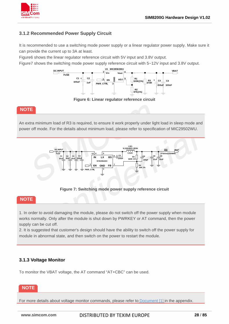
3.1.2 Recommended Power Supply Circuit It is recommended to use a switching mode power supply or a linear regulator power supply. Make sure it can provide the current up to 3A at least. Figure6 shows the linear regulator reference circuit with 5V input and 3.8V output. Figure7 shows the switching mode power supply reference circuit with 5~12V input and 3.8V output.
Vin Vout
GN
D
ADJ
3
+
PWR_CTRL
R2
R1
VBAT
100K(1%)
47K(1%)
+
U1 MIC29502WU
5
4
1
2
C1 C2100uF 1uF
DC INPUT
R3470R
EN
FUSE
C3
330uF
C4
100nF
Figure 6: Linear regulator reference circuit
An extra minimum load of R3 is required, to ensure it work properly under light load in sleep mode and power off mode. For the details about minimum load, please refer to specification of MIC29502WU.
10uF
EN
IN LX BS
GND FB
VBATDC INPUT
PWR_CTRL
10uF 10uF 100nF
L101VLS5045EX-3R3N
3.3UH
160K 1%100nF100pF 22uF 10uF
30K 1%
C1 C2 C3 C4 C5R3
R4
C6 C8 C9U1
SY8105IADC
Fuse
FB1
270ohm@100MHz
1
654
2
3
Figure 7: Switching mode power supply reference circuit
1. In order to avoid damaging the module, please do not switch off the power supply when module works normally. Only after the module is shut down by PWRKEY or AT command, then the power supply can be cut off. 2. It is suggested that customer's design should have the ability to switch off the power supply for module in abnormal state, and then switch on the power to restart the module.
3.1.3 Voltage Monitor
To monitor the VBAT voltage, the AT command “AT+CBC” can be used.
For more details about voltage monitor commands, please refer to Document [1] in the appendix.
NOTE
NOTE
NOTE
DISTRIBUTED BY TEXIM EUROPE
SIM8200G Hardware Design V1.02
www.simcom.com 29 / 85
3.2 Power On and Off Module
3.2.1 Power On Drive the PWRKEY pin to a low level and hold it for 2 seconds, then release, the module will be powered on. This pin is already pulled up internally. The electrical characteristics are listed in table 10, and the following figure shows the power on circuit.
PWRKEY
1K
Module
100K
1.1V
PMU≥2s
Figure 8: Power on the module use button
PWRKEY100K
1.1V
1KPMU
Module≥2s
GPIO
MCU
Figure 9: Power on the module use GPIO drive
Table 9: Definition of PWRKEY pin
Pin name Pin no. Electrical description Description Comment
PWRKEY A45 DI Power on/off the module, active low
Pull up to 1.1V internally without PM8150B
The power on sequence is shown in the following figure.
DISTRIBUTED BY TEXIM EUROPE

SIM8200G Hardware Design V1.02
www.simcom.com 30 / 85
PWRKEY
RESIN_N
VBAT
Ton
Twait
S2E_1P224
S3E_0P824
S4E_1P904
VDD_EXT
L10E_3P1
T1
T2
T3
USB Port Undefined Active
Ton(usb)
Figure 10: Power on sequence Table 10: Power on timing and electronic characteristic
Symbol Parameter Min. Typ. Max. Unit
Twait The waiting time from power supply available to power-on action
100 - - ms
Ton The time of holding on PWRKEY pin to a low level 2 - - s
T1 The time from power-on action to S2E,S3E and S4E ready
- 45 - ms
T2 The time from power-on action to VDD_EXT ready - 48 - ms T3 The time from power-on action to L10E_3P1 ready - 50 - ms Ton(usb) The time from power-on action to USB port ready - TBD - s VIH Input high level voltage on PWRKEY pin 1.1 - 2.1 V VIL Input low level voltage on PWRKEY pin 0 - 0.3 V
3.2.2 Power Off
The following methods can be used to power off the module. ● Method 1: Power off the module by holding the PWRKEY to a low level 2 second then release. ● Method 2: Power off the module by AT command “AT+CPOF”. For details about “AT+CPOF”, please refer to Document [1] in the appendix.
DISTRIBUTED BY TEXIM EUROPE
SIM8200G Hardware Design V1.02
www.simcom.com 31 / 85
If the temperature is outside the range of -30~+70℃, some warning will be reported via AT port. If the temperature is outside the range of -40~+85℃, module will be powered off automatically. For details about “AT+CPOF”, please refer to Document [1] in the appendix.
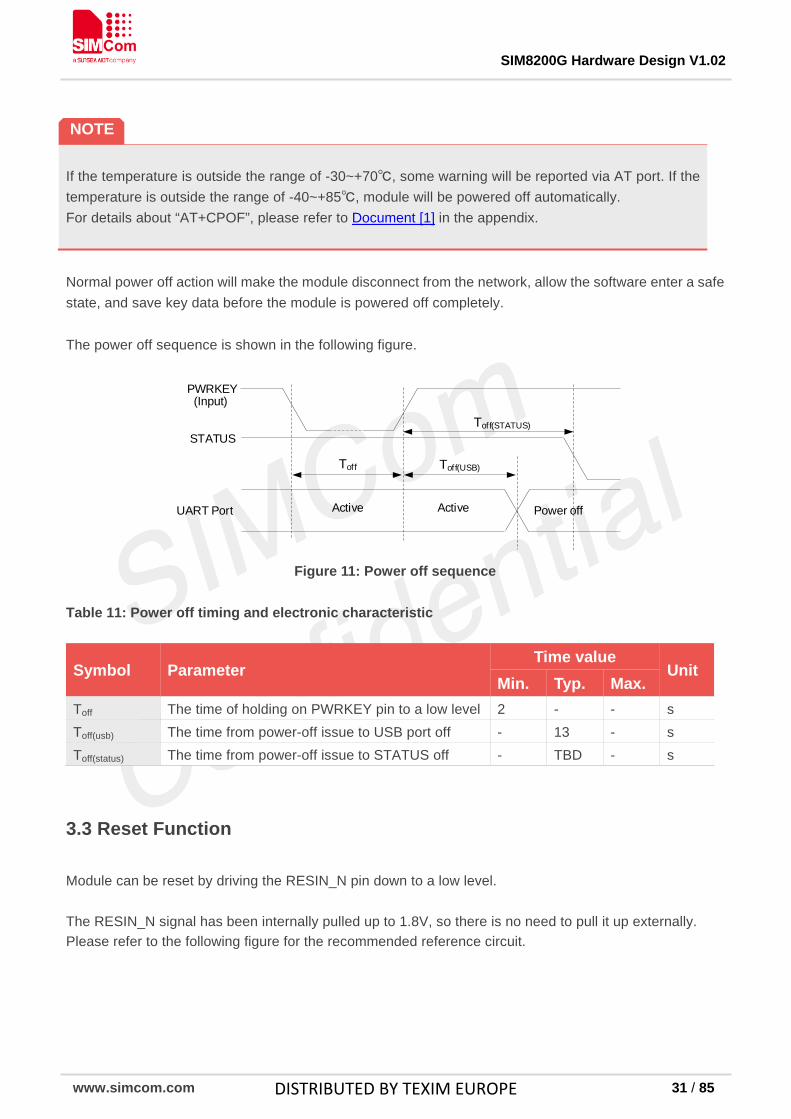
Normal power off action will make the module disconnect from the network, allow the software enter a safe state, and save key data before the module is powered off completely. The power off sequence is shown in the following figure.
(Input)
UART Port Power offActive
PWRKEY
Active
Toff Toff(USB)
STATUSToff(STATUS)
Figure 11: Power off sequence Table 11: Power off timing and electronic characteristic
Symbol Parameter Time value
Unit Min. Typ. Max.
Toff The time of holding on PWRKEY pin to a low level 2 - - s Toff(usb) The time from power-off issue to USB port off - 13 - s Toff(status) The time from power-off issue to STATUS off - TBD - s
3.3 Reset Function
Module can be reset by driving the RESIN_N pin down to a low level. The RESIN_N signal has been internally pulled up to 1.8V, so there is no need to pull it up externally. Please refer to the following figure for the recommended reference circuit.
NOTE
DISTRIBUTED BY TEXIM EUROPE

SIM8200G Hardware Design V1.02
www.simcom.com 32 / 85
Reset Impulse
RESIN_N Reset Logic
50K
1.8V Module
1K
200~600ms
GPIO
MCU
Figure 12: Reset the module use GPIO drive
Reset Logic
50K
1.8V Module
1KTreset
200~600ms
RESIN_N
Figure 13: Reset the module use button
Table 12: Definition of RESIN_N pin
Pin name Pin no. Electrical description Description Comment
RESIN_N A43 DI P3 Reset the module, active low
Table 13: RESET electronic characteristics Symbol Description Min. Typ. Max. Unit Treset The time of holding on RESIN_N pin to a low level 200 - 600 ms VIH Input high level voltage 1.2 - 1.9 V VIL Input low level voltage 0 - 0.4 V
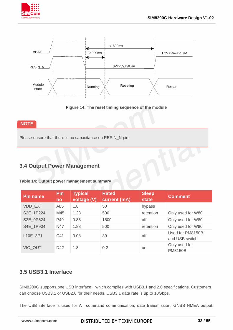
The reset timing sequence of the module is shown in the following figure.
DISTRIBUTED BY TEXIM EUROPE
SIM8200G Hardware Design V1.02
www.simcom.com 33 / 85
Module state RestarReseting
VBAT
Running
RESIN_N
≥200ms
0V≤VIL≤0.4V
1.2V≤VIH≤1.9V
≤600ms
Figure 14: The reset timing sequence of the module
Please ensure that there is no capacitance on RESIN_N pin.
3.4 Output Power Management
Table 14: Output power management summary
Pin name Pin no
Typical voltage (V)
Rated current (mA)
Sleep state Comment
VDD_EXT AL5 1.8 50 bypass S2E_1P224 M45 1.28 500 retention Only used for W80 S3E_0P824 P49 0.88 1500 off Only used for W80 S4E_1P904 N47 1.88 500 retention Only used for W80
L10E_3P1 C41 3.08 30 off Used for PM8150B and USB switch
VIO_OUT D42 1.8 0.2 on Only used for PM8150B
3.5 USB3.1 Interface
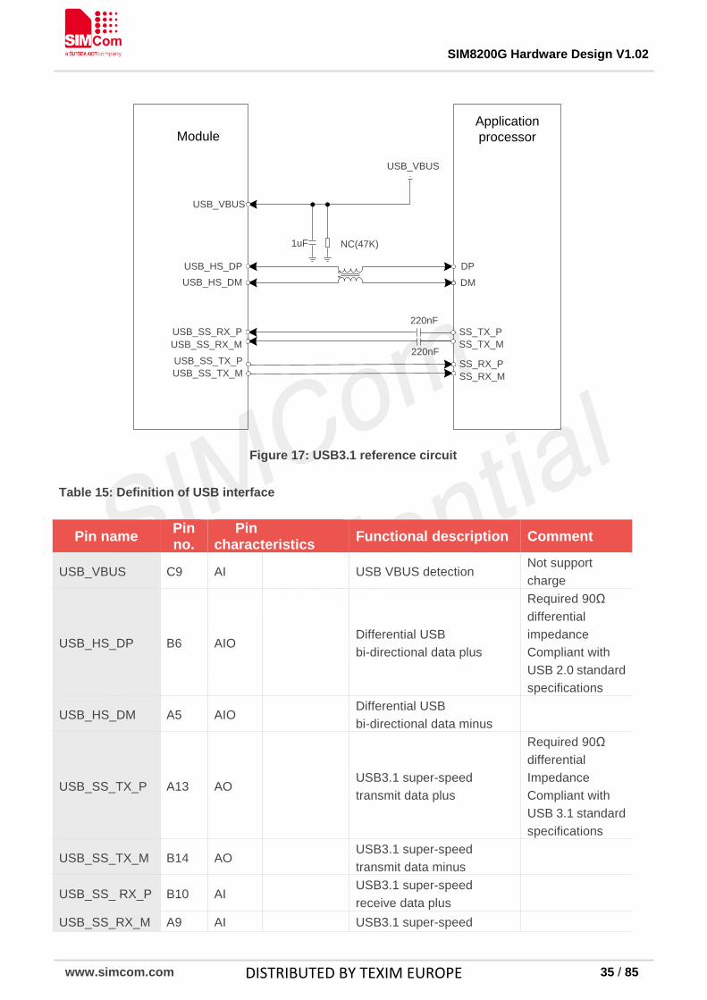
SIM8200G supports one USB interface,which complies with USB3.1 and 2.0 specifications. Customers can choose USB3.1 or USB2.0 for their needs. USB3.1 data rate is up to 10Gbps. The USB interface is used for AT command communication, data transmission, GNSS NMEA output,
NOTE
DISTRIBUTED BY TEXIM EUROPE

SIM8200G Hardware Design V1.02
www.simcom.com 34 / 85
firmware upgrade and software debugging. SIM8200G supports USB suspend and resume mechanism, which can save power consumption. If there is no data transmission on the USB bus, module will enter suspend mode automatically. The following figure is the USB reference circuit.
USB_VBUS
USB_HS_DP
USB_SS_TX_P
USB_HS_DM
USB_SS_TX_MUSB_SS_RX_PUSB_SS_RX_M
CC1CC2
USB SS Switch
VBUS
SPMI_DATA
SEL
Module Type-C USB Connector
SS_TX1_PSS_TX1_MSS_RX1_PSS_RX1_M
SS_TX2_PSS_TX2_MSS_RX2_PSS_RX2_M
DP1/DP2DN1/DN2
CC1CC2
1uF NC(47K)
SPMI_CLKSUB1SUB2
PM8150B
SUB1SUB2
1K 1K
PI3DBS12212A <0.5pF
220nF
220nF
220nF
<0.5pF
220nF
220nF
220nF
L10E_3P1
GPIO5
Figure 15: Type-C USB reference circuit with PM8150B
USB_VBUS
USB_HS_DP
USB_SS_TX_P
USB_HS_DM
USB_SS_TX_MUSB_SS_RX_PUSB_SS_RX_M
CC1CC2
USB SS Switch
VBUS
I2C1_SDA
SEL
Module Type-C USB Connector
SS_TX1_PSS_TX1_MSS_RX1_PSS_RX1_M
SS_TX2_PSS_TX2_MSS_RX2_PSS_RX2_M
DP1/DP2DN1/DN2
CC1CC2
1uF NC(47K)
I2C1_SCL
PI3DBS12212A <0.5pF
220nF
220nF
220nF
<0.5pF
220nF
220nF
220nF
USB_SS_SW
2.2K2.2K
USB_ID INT
PI5USB30216D
Type-C CC detectorVDD_EXT
L10E_3P1
Figure 16: Type-C USB reference circuit with CC detector
DISTRIBUTED BY TEXIM EUROPE
SIM8200G Hardware Design V1.02
www.simcom.com 35 / 85
USB_VBUS
USB_HS_DP
USB_SS_RX_P
USB_HS_DM
USB_SS_RX_MUSB_SS_TX_PUSB_SS_TX_M
SS_TX_PSS_TX_M
SS_RX_PSS_RX_M
DP
DM
1uF NC(47K)
220nF
220nF
Application processorModule
USB_VBUS
Figure 17: USB3.1 reference circuit
Table 15: Definition of USB interface
Pin name Pin no.
Pin characteristics Functional description Comment
USB_VBUS C9 AI USB VBUS detection Not support charge
USB_HS_DP B6 AIO Differential USB bi-directional data plus
Required 90Ω differential impedance Compliant with USB 2.0 standard specifications
USB_HS_DM A5 AIO Differential USB bi-directional data minus
USB_SS_TX_P A13 AO USB3.1 super-speed transmit data plus
Required 90Ω differential Impedance Compliant with USB 3.1 standard specifications
USB_SS_TX_M B14 AO USB3.1 super-speed transmit data minus
USB_SS_ RX_P B10 AI USB3.1 super-speed receive data plus
USB_SS_RX_M A9 AI USB3.1 super-speed
DISTRIBUTED BY TEXIM EUROPE

SIM8200G Hardware Design V1.02
www.simcom.com 36 / 85
receive data minus
USB_ID* C11 DI P3 USB ID If unused, please keep open
OTG_EN* D10 DO P3 USB OTG power supply DC-DC enable signal
USB_SS_SW C13 DO P3 USB Type-C switch control signal
“*” means under development. Table 16: Recommended CC detector list
No. Manufacturer Part number Package 1 PERICOM PI5USB30216D QFN12
Table 17: Recommended SS USB switch list No. Manufacturer Part number Package 1 PERICOM PI3DBS12212A QFN3X3 Table 18: Recommended OTG 5V DC-DC and USB interface TVS list
Name Manufacturer Part number Package DC-DC AWINIC AW3605DNR TDFN2X3-8L TVS(DP/DM) WILL ESD5302N-3/TR DFN1006-3L
USB SS TX/RX layout guidelines: Require differential trace impedance is 90±10% Ω. The intra-lane length mismatch of the differential signal lanes is less than 700um. Gap from other signals keeps 4xline width. Gap between Rx-to-Tx keeps 4xline width. External components should be placed near the USB connector. Trace routes away from other sensitive signals.
USB HS DP/DM layout guidelines: Require differential trace impedance is 90±10% Ω. The intra-lane length mismatch of the differential signal lanes is less than 1mm. Gap from other signals keeps 3xline width. External components should be placed near the USB connector. Trace routes away from other sensitive signals.
NOTE
DISTRIBUTED BY TEXIM EUROPE

SIM8200G Hardware Design V1.02
www.simcom.com 37 / 85
3.6 PCIe Interface
SIM8200G support PCIe Gen3 two lane interfaces, and can be used as EP or RC mode. The data rate up to 8Gbps per lane. PCIe Gen3 lane0 can be connected to W80 as a data interface. PCIe_CLKREQ and PCIe_WAKE need to be pulled up to VDD_EXT out of the module. The details design, please refer to the reference circuit document. The following figure is the PCIe reference circuit.
Module W80
220nF
PCIe_REFCLK_M
PCIe_REFCLK_P
PCIe_WAKEPCIe_RSTPCIe_CLKREQ
PCIe_RXMPCIe_RXP
PCIe_CLKM
PCIe_CLKP
10K
10K
PCIe_WAKEPCIe_RST
PCIe_CLKREQ
PCIe_TX0_MPCIe_TX0_P
PCIe_RX0_MPCIe_RX0_P
PCIe_TXMPCIe_TXP
220nF220nF
220nF
+1.8V
Figure 18: PCIe interface reference circuit (RC)
Module Application processor
220nF
PCIe_REFCLK_M
PCIe_REFCLK_P
PCIe_WAKEPCIe_RSTPCIe_CLKREQ
PCIe_RXMPCIe_RXP
PCIe_CLKM
PCIe_CLKP
10K
10K
PCIe_WAKEPCIe_RST
PCIe_CLKREQ
PCIe_TX0_MPCIe_TX0_P
PCIe_RX0_MPCIe_RX0_P
PCIe_TXMPCIe_TXP
220nF
220nF
220nF
+1.8V
Figure 19: PCIe interface reference circuit (EP)
1. The AC capacitors of PCIe_TXM and PCIe_TXP should be placed near the AP.
NOTE
DISTRIBUTED BY TEXIM EUROPE

SIM8200G Hardware Design V1.02
www.simcom.com 38 / 85
2. The voltage domain of PCIe assistant signals is 1.8V. 3. PCIe Lane1 is under development. Table 19: Definition of PCIe interface
Pin name Pin no.
Pin characteristics
Functional description Comment
PCIe_REFCLK_P
B22 AIO PCIe reference clock plus
Required 90Ω differential impedance
PCIe_REFCLK_M
A21 AIO PCIe reference clock minus
PCIe_TX0_M B18 AO PCIe transmit0 minus PCIe_TX0_P A17 AO PCIe transmit0 plus PCIe_TX1_M* B20 AO PCIe transmit1 minus PCIe_TX1_P* A19 AO PCIe transmit1 plus PCIe_RX0_M A25 AI PCIe receive0 minus PCIe_RX0_P B26 AI PCIe receive0 plus PCIe_RX1_M* A23 AI PCIe receive1 minus PCIe_RX1_P* B24 AI PCIe receive1 plus PCIe_CLKREQ C21 DI P3 PCIe clock request PCIe_CLKREQ and
PCIe_WAKE need pull up to VDD_EXT externally, Default as RC mode
PCIe_WAKE C25 DI P3 PCIe wake-up
PCIe_RST C23 DO P3 PCIe reset
PCIe interface layout guidelines: Require differential trace impedance is 90±10% Ω. The intra-lane length mismatch of the differential signal lanes is less than700um. Gap from other signals keeps 4xline width. Gap between Rx-to-Tx keeps 4xline width. Trace routes away from other sensitive signals.
3.7 SDIO Interface SIM8200G supports 8-bit SDIO1 interface, which meets the SDIO3.0 specifications and supports SDIO host mode. The clock output up to 200MHz for SD card, and up to 100MHz for eMMC*. Support 4-bit dual-voltage 1.8V or 3.0V SD card or 8-bit 1.8V eMMC*. Figure20 shows the SD card reference circuit. Figure21 shows the eMMC reference circuit.
DISTRIBUTED BY TEXIM EUROPE
SIM8200G Hardware Design V1.02
www.simcom.com 39 / 85
DATA2 DATA3 CMD VDD CLK VSS DATA0 DATA1 DET_SW
GND GND GND GND
SD cardCONN
SDIO_DATA2SDIO_DATA3
SDIO_CMD
SDIO_CLK
SDIO_DATA0SDIO_DATA1
470K
SDC_DET
Module
4.7uF 33pF
33R
VDD_EXT
TVS close to SD crad CONN
VDD_2P95
e-DCDCAN_SY8089
SDIO_VDD_ENe-LDO
TPS728EN
VSETOUT
EN OUT
GPIO100SDIO_VDD
<5PF
1K
Figure 20: SD card reference circuit
VCC
VCCQ
CMDRST_NCLKDATA0DATA1DATA2DATA3DATA4DATA5DATA6DATA7
VDDIM
eMMC
SDC_CMDRESOUT_N
SDC_CLKSDC_DATA0SDC_DATA1SDC_DATA2SDC_DATA3
SDC_VDD_ENSDC_DETGPIO100GPIO101
Module 3.3VAN_SY8089
IN OUT
1.8VAXK580147YG
IN OUT
10
K10
K10
K10
K10
K10
K
VBAT
SDIO_VDD
1uF 100nF
4.7uF 2.2uF 100nF 2.2uF 100nF
Figure 21: eMMC reference circuit
1. If not use SDIO interface, the SD_VDD pin should connect to VDD_EXT out of the module. 2. “*” means under development. Table 20: Definition of SDIO interface
Pin name Pin no.
Pin characteristics Functional description Comment
SDIO_VDD F7 PI 1.8/3.0V Power input for internal SDIO circuit
SDIO_DATA0 B1 DIO P2 SDC data bit 0 or eMMC* data bit 0
Required 50Ω impedance
SDIO_DATA1 C1 DIO P2 SDC data bit 1 or eMMC data bit 1
SDIO_DATA2 D3 DIO P2 SDC data bit 2 or eMMC data bit 2
SDIO_DATA3 F3 DIO P2 SDC data bit 3 or eMMC data bit 3
NOTE
DISTRIBUTED BY TEXIM EUROPE

SIM8200G Hardware Design V1.02
www.simcom.com 40 / 85
SDIO_CMD G5 DIO P2 SDC command output SDIO_CLK E5 DO P2 SDC clock output SDIO_VDD_EN
H7 DO P3 Enable the SD card power or eMMC data bit 4 If used as eMMC
data signals, required 50Ω impedance
SDIO_DET E1 DI P3 SD card insertion detect or eMMC data bit 5
GPIO100 H3 DIO P3 eMMC data bit 6 GPIO101 K7 DIO P3 eMMC data bit 7
RESOUT_N* AW17 DO P3 eMMC RST_N
If use this pin please confirm with SIMCom support teams
Table 21: Recommended TVS and SD card socket list
Name Manufacturer Model TVS ON ESD9L5.0ST5G SD card socket ALPS SCHA4B0400 SDIO interface layout guidelines: Require trace impedance is 50 Ω ±10%. CLK to DATA/CMD length mismatch is less than 0.5mm. 30–35 Ω termination resistance on clock net and placed close to the module. Gap from other signals keeps 2xline width. Bus capacitance is less than 5pF. Trace routes away from other sensitive signals.
3.8 RGMII Interface
SIM8200G supports RGMII interface, data rate up to 1000Mbps, customers can use AR8035 convert to RJ45 interface out of the module. The reference circuit is as follows:
DISTRIBUTED BY TEXIM EUROPE

SIM8200G Hardware Design V1.02
www.simcom.com 41 / 85
E-PHY(AR8035)
Module
RGMII_PWR_IN
RGMII_VREG_3P3_ENSGM2040-3.3YUDH4G
VPH_PWR
EN
TP+TP-RP+RP-
RJ
45
25MHz
LSF0204PW
R
1P8VVDDH_REG
SN74AVCH1T45DC
KT
1P8V
H5007
MDI1+/-MDI2+/-MDI3+/-
MDI0+/-
TX_ENTXD3
GTX_CLKTXD0TXD1TXD2
RGMII_TX_CTLRGMII _TX_3
RGMII _TX_CLKRGMII _TX_0RGMII _TX_1RGMII _TX_2
RX_CLKRXD0
RXD1RXD2RXD3RX_DV
RGMII _RX_CLKRGMII _RX_0
RGMII _RX_1RGMII _RX_2RGMII _RX_3
RGMII_RX_CTL
MDC MDC
MDIO MDIO
RSTn
INT
RSTn
INT
VDD_33
4.7K
Figure 22: RGMII to RJ45 diagram circuit Table 22: Definition of RGMII interface
Pin name Pin no.
Pin characteristics Functional description Comment
RGMII_MD_IO D30 DIO P8 RGMII management data
Required 50Ωimpedance
RGMII_MD_CLK D34 DO P8 RGMII management data clock RGMII _RX_CTL A35 DI P8 RGMII receive control RGMII _RX_CLK B36 DI P8 RGMII receive clock RGMII_RX_0 B40 DI P8 RGMII receive data bit 0 RGMII_RX_1 A37 DI P8 RGMII receive data bit 1 RGMII_RX_2 B38 DI P8 RGMII receive data bit 2 RGMII_RX_3 A39 DI P8 RGMII receive data bit 3 RGMII _TX_CTL A33 DO P8 RGMII transmit control RGMII _TX_CLK B34 DO P8 RGMII transmit clock RGMII_TX_0 A31 DO P8 RGMII transmit data bit 0 RGMII_TX_1 B30 DO P8 RGMII transmit data bit 1 RGMII_TX_2 A29 DO P8 RGMII transmit data bit 2 RGMII_TX_3 B32 DO P8 RGMII transmit data bit 3 RGMII_INT_N C39 DI P3 Interrupt input from RGMII PHY
RGMII_RST_N C29 DO P3 Reset output to RGMII PHY
RGMII_PWR_EN D36 DO P3 Used to enable external LDO to supply 2.5V power to RGMII_PWR_IN
RGMII_PWR_IN D32 PI 1.8V Power supply input for internal RGMII circuit
RGMII_3P3_EN D38 DO P3 Used to enable external DC-DC/LDO to supply 3.3V
DISTRIBUTED BY TEXIM EUROPE

SIM8200G Hardware Design V1.02
www.simcom.com 42 / 85
power to RGMII PHY
RGMII interface layout guidelines: Require trace impedance is 50 Ω ± 10%. TX to TX_CLK, TX_DATA length mismatch is less than 5mm. RX to RX_CLK, RX_DATA length mismatch is less than 5mm. Gap within TX bus or RX bus keeps 2xline width. Gap to other signals keeps 3xline width. Gap RX-to-TX keeps 2xline width. Trace routes away from sensitive signals.
3.9 (U)SIM Interface
SIM8200G supports two (U)SIM cards but single standby. (U)SIM1 and (U)SIM2 are dual-voltage 1.8 V or 3.0 V interfaces. Table 23: (U)SIM electronic characteristics in 1.8V mode ((U)SIM_PWR=1.8V)
Symbol Parameter Min. Typ. Max. Unit (U)SIM_VDD Power supply for (U)SIM card 1.65 1.8 1.95 V VIH High-level input voltage 1.26 - 1.95 V VIL Low-level input voltage 0 - 0.36 V VOH High-level output voltage 1.44 - 1.8 V VOL Low-level output voltage 0 - 0.4 V
Table 24: (U)SIM electronic characteristics 3.0V mode ((U)SIM_PWR=3.0V)
Symbol Parameter Min. Typ. Max. Unit (U)SIM_VDD Power supply for (U)SIM card 2.7 3.0 3.05 V
VIH High-level input voltage 2.1 - 3.05 V VIL Low-level input voltage 0 - 0.6 V VOH High-level output voltage 2.4 - 3.0 V VOL Low-level output voltage 0 - 0.4 V
The module supports (U)SIM card hot-swap function through the (U)SIM_DET pin, which is a level trigger pin. The USIM_DET pin requires pull up externally. The following figure shows (U)SIM card reference circuit.
DISTRIBUTED BY TEXIM EUROPE

SIM8200G Hardware Design V1.02
www.simcom.com 43 / 85
TVS
(U)SIM_VDD
(U)SIM_CLK
(U)SIM_DATA
(U)SIM_RST0Ω
220nF
(U)SIM Socket
XNT-0211BAAG06A
0Ω
0Ω
(NC)
100Ω(U)SIM_DET
33pF
GN
D1
GN
D1
CD
1C
D1
Module
(NC) (NC) (NC)
VCC
RST
CLK
GND
VPP
I/O
VDD_EXT470KΩ
Figure 23: (U)SIM interface reference circuit
After inserting (U)SIM card, the (U)SIM_DET pin will change from high to low level. The falling edge will indicate that the (U)SIM card has been inserted. After removing the (U)SIM card, the (U)SIM_DET pin will change from low to high level. This rising edge will indicate the removal of the (U)SIM card. The (U)SIM card hot swap function needs to be enabled by AT command. Please refer to the SIM8200 Series_AT Command Manual for the setting of the detection level of (U)SIM_DET pin. Table 25: Definition of (U)SIM interface
Pin name Pin no.
Pin characteristics Functional description Comment
(U)SIM1_VDD B51 PO P4 Power supply for (U)SIM1 card
1.8/3.0V voltage domain, (U)SIM interface should be protected against ESD. If unused, please keep open
(U)SIM1_DATA E51 DIO P4
(U)SIM1 card data signal, which has been pulled up to (U)SIM1_VDD by a 20K resistor internally
(U)SIM1_CLK D49 DO P4 (U)SIM1 clock signal (U)SIM1_RST C51 DO P4 (U)SIM1 reset signal
(U)SIM1_DET E47 DI P3
(U)SIM1 card detect signal, which need pulled up to VDD_EXT by a 470K resistor externally
(U)SIM2_VDD F49 PO P5 Power supply for (U)SIM2 card
(U)SIM2_DATA G47 DIO P5 (U)SIM1 card data, which has been pulled up to (U)SIM1_VDD by a 20K resistor internally
(U)SIM2_CLK H49 DO P5 (U)SIM2 clock signal (U)SIM2_RST G51 DO P5 (U)SIM2 reset signal
(U)SIM2_DET F45 DI P3 (U)SIM1 card detect, which need pulled up to VDD_EXT by a 470KR resistor externally
DISTRIBUTED BY TEXIM EUROPE

SIM8200G Hardware Design V1.02
www.simcom.com 44 / 85
The following table shows recommended TVS of ESD protect and (U)SIM socket. Table 26: Recommended TVS and (U)SIM socket list Name Manufacturer Model
TVS ST ESDA6V1-5W6
(U)SIM socket Suntech XNT-0211BAAG06A
If the (U)SIM card hot-swap function is not used, customers should keep the (U)SIM_DET pin open. The (U)SIM card layout guidelines: Make sure that the (U)SIM card socket should be far away from the antennas. (U)SIM traces should be away from RF, VBAT and high-speed signals. The traces should be as short as possible. Keep (U)SIM socket’s GND pin directly connect to the main ground. Shielding the (U)SIM card signals by ground. Recommended to place a 33pF ~1uF capacitor on (U)SIM_VDD net and place close to the holder. The rise/fall time of (U)SIM_CLK should not exceed 40ns. The parasitic capacitance of TVS should not exceed 60pF, and the TVS should be placed close to
the (U)SIM socket.
3.10 I2S Interface
SIM8200G supports one I2S/PCM interface for external codec, which meets the requirements in the Phillips I2S bus specification. Table 27: I2S format
For more details about I2S AT commands, please refer to document [1] in the appendix.
Characteristics Specification Line interface format Linear(fixed)
Data length 16bits(fixed)
I2S flock/sync source Master mode(fixed)
I2S clock sate 1.536 MHz (default)
I2S MCLK rate 12.288MHz (default)
Data ordering MSB
NOTE
DISTRIBUTED BY TEXIM EUROPE

SIM8200G Hardware Design V1.02
www.simcom.com 45 / 85
3.10.1 I2S Timing The module supports I2S sampling rate of 48 KHz and 32 bit coding signal (16 bit length), the timing sequence is shown in the following figure.
Figure 24: I2S timing Table 28: I2S timing parameters
3.10.2 I2S Reference Circuit
The following figure shows the external codec reference design.
Signal Parameter Description Min. Typ. Max. Unit
I2S_MCLK
Frequency Frequency – 12.288 12.288 MHz T Clock period 81.380 81.380 – ns t(HC) Clock high 0.45T – 0.55T ns t(LC) Clock low 0.45T – 0.55T ns
I2S_CLK
Frequency Frequency 8 48 48 KHz T Clock period 20.83 20.83 125 us t(HC) Clock high 0.45T – 0.55T ns t(LC) Clock low 0.45T – 0.55T ns
I2S_WS
t(sr) DIN/DOUT and WS input setup time
16.276 – – ns
t(hr) DIN/DOUT and WS input hold time 0 – – ns t(dtr) DIN/DOUT and WS output delay – – 65.10 ns
t(htr) DIN/DOUT and WS output hold time
0 – – ns
DISTRIBUTED BY TEXIM EUROPE
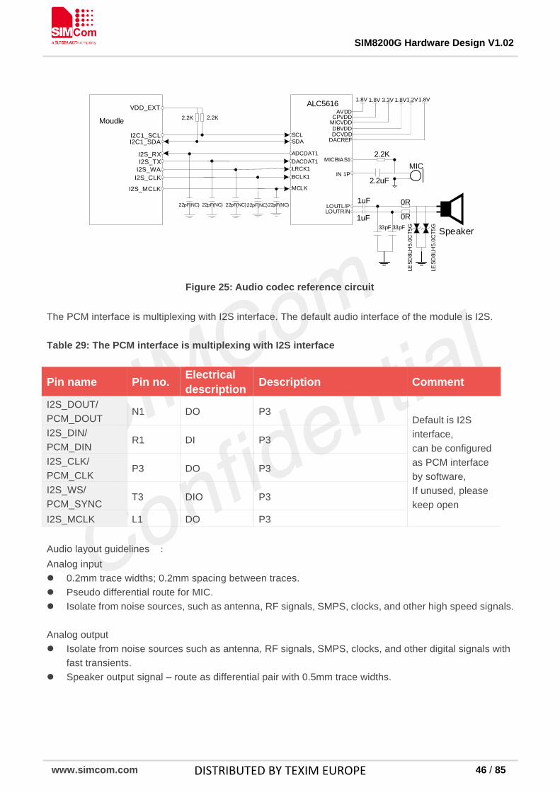
SIM8200G Hardware Design V1.02
www.simcom.com 46 / 85
I2S_MCLK
22pF(NC)
ADCDAT1
LRCK1BCLK1
DACDAT1
MCLK
SCLSDA
IN 1P
MICBIAS1
LOUTR/N
MIC
ALC5616
2.2K
2.2uF
I2C1_SCLI2C1_SDA
I2S_RXI2S_TX
I2S_WAI2S_CLK
Moudle
22pF(NC)22pF(NC) 22pF(NC)22pF(NC) LOUTL/P 0R
0R33pF Speaker33pF
LESD
8LH
5.0C
T5G
LESD
8LH
5.0C
T5G
1uF
1uF
1.8V 1.8V 3.3V 1.8V
AVDDCPVDD
DBVDDMICVDD
DCVDD
1.2V
DACREF
1.8VVDD_EXT
2.2K2.2K
Figure 25: Audio codec reference circuit
The PCM interface is multiplexing with I2S interface. The default audio interface of the module is I2S. Table 29: The PCM interface is multiplexing with I2S interface
Pin name Pin no. Electrical description Description Comment
I2S_DOUT/ PCM_DOUT
N1 DO P3 Default is I2S interface, can be configured as PCM interface by software, If unused, please keep open
I2S_DIN/ PCM_DIN
R1 DI P3
I2S_CLK/ PCM_CLK
P3 DO P3
I2S_WS/ PCM_SYNC
T3 DIO P3
I2S_MCLK L1 DO P3 Audio layout guidelines : Analog input 0.2mm trace widths; 0.2mm spacing between traces. Pseudo differential route for MIC. Isolate from noise sources, such as antenna, RF signals, SMPS, clocks, and other high speed signals. Analog output Isolate from noise sources such as antenna, RF signals, SMPS, clocks, and other digital signals with
fast transients. Speaker output signal – route as differential pair with 0.5mm trace widths.
DISTRIBUTED BY TEXIM EUROPE
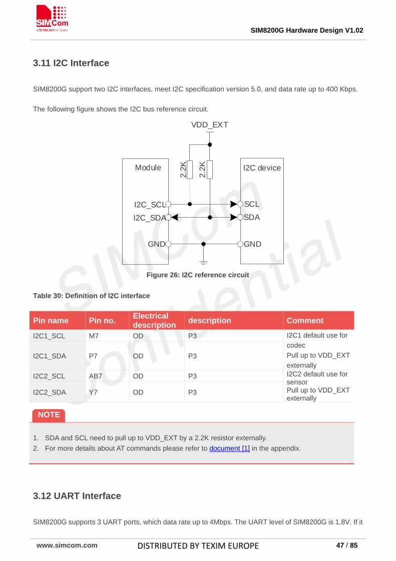
SIM8200G Hardware Design V1.02
www.simcom.com 47 / 85
3.11 I2C Interface
SIM8200G support two I2C interfaces, meet I2C specification version 5.0, and data rate up to 400 Kbps. The following figure shows the I2C bus reference circuit.
Module
I2C_SDA
I2C device
SDA
GNDGND
I2C_SCL SCL
VDD_EXT
2.2K
2.2K
Figure 26: I2C reference circuit
Table 30: Definition of I2C interface
Pin name Pin no. Electrical description description Comment
I2C1_SCL M7 OD P3 I2C1 default use for codec Pull up to VDD_EXT externally
I2C1_SDA P7 OD P3
I2C2_SCL AB7 OD P3 I2C2 default use for sensor Pull up to VDD_EXT externally
I2C2_SDA Y7 OD P3
1. SDA and SCL need to pull up to VDD_EXT by a 2.2K resistor externally. 2. For more details about AT commands please refer to document [1] in the appendix.
3.12 UART Interface
SIM8200G supports 3 UART ports, which data rate up to 4Mbps. The UART level of SIM8200G is 1.8V. If it
NOTE
DISTRIBUTED BY TEXIM EUROPE

SIM8200G Hardware Design V1.02
www.simcom.com 48 / 85
communicates with the 3.3V serial port level, a level conversion chip needs to be added in the middle. It is recommended to use TI's TXS0104EPWR level shift, the reference circuit is as follows.
VCCA
TXS0104EPWR
100pFOE
A1A2A3A4
VCCB
GND
B1B2B3B4
VDD_1V8
UART_CTSUART_RTS
UART_TXDUART_RXD
100pF
VDD_3V3
UART_CTS_3V3UART_RTS_3V3
UART_TXD_3V3UART_RXD_3.3V
Figure 27: UART level conversion circuit
The following level shifting circuits can also be used:
VDD_1V8
4.7K
47K
TXD
4.7K
Module
VDD_EXT
RXD
VDD
DTE
Figure 28: UART TX level conversion circuit
VDD_1V8
4.7K
47K4.7K
DTE
RXD
Module
VDD_1V8
TXD
VDD
Figure 29: UART RX level conversion circuit
DISTRIBUTED BY TEXIM EUROPE

SIM8200G Hardware Design V1.02
www.simcom.com 49 / 85
Table 31: Definition of UART interface
Pin name Pin no. Electrical description description Comment
UART1_CTS AA1 DO Clear to send
Default use for AT command
UART1_RTS AC1 DI Request to send UART1_TXD AB3 DO Transmit data UART1_RXD AD3 DI Receive data UART1_DCD W5 DO Carrier detect
UART1_RI AA5 DO Ring indicator UART1_DTR AC5 DI Data terminal ready UART2_CTS V3 DO Clear to send
UART2_RTS Y3 DI Request to send UART2_TXD U1 DO Transmit data UART2_RXD W1 DI Receive data BT_UART_CTS
R5 DO Clear to send
Default use for BT
BT_UART_RTS
U5 DI Request to send
BT_UART_TXD
T7 DO Transmit data
BT_UART_RXD
V7 DI Receive data
DBG_UART_RXD
L5 DI Receive data Used for debug only
DBG_UART_TXD
N5 DO Transmit data
3.13 SPI Interface*
SIM8200G SPI interface only supports master mode, data rate up to 50MHz. Usually, SPI interface is used to connect ROM or LCD and other devices.
DISTRIBUTED BY TEXIM EUROPE
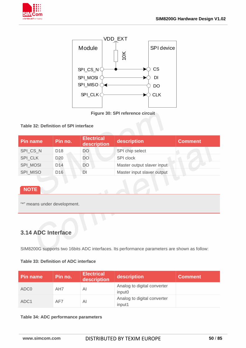
SIM8200G Hardware Design V1.02
www.simcom.com 50 / 85
Module
SPI_MOSI
SPI device
DI
CLKSPI_CLK
SPI_MISO
CS
VDD_EXT
10K
SPI_CS_N
DO
Figure 30: SPI reference circuit
Table 32: Definition of SPI interface
Pin name Pin no. Electrical description description Comment
SPI_CS_N D18 DO SPI chip select
SPI_CLK D20 DO SPI clock
SPI_MOSI D14 DO Master output slaver input
SPI_MISO D16 DI Master input slaver output
“*” means under development.
3.14 ADC Interface
SIM8200G supports two 16bits ADC interfaces. Its performance parameters are shown as follow:
Table 33: Definition of ADC interface
Pin name Pin no. Electrical description description Comment
ADC0 AH7 AI Analog to digital converter input0
ADC1 AF7 AI Analog to digital converter input1
Table 34: ADC performance parameters
NOTE
DISTRIBUTED BY TEXIM EUROPE

SIM8200G Hardware Design V1.02
www.simcom.com 51 / 85
Parameter Comments Min Typ Max Unit Input voltage range Programmable 0 - 1.875 V Resolution - 16 - bits Analog input bandwidth - 500 - KHz Sample rate - 4.8 - MHz Accuracy - 20 - mV
3.15 WLAN/BT Interface
SIM8200G supports W80 interface including PCIe, UART, I2S, GPIOs, and customers can connect to the W80 WLAN/BT module through this interface. The reference circuit is as follows:
PCIe_TX0_MPCIe_TX0_P
PCIe_RX0_PPCIe_RX0_M
PCIe_REFCLK_MPCIe_REFCLK_P
PCIe_WAKEPCIe_RST
PCIe_CLKREQ
S2E_1P224S3E_0P824S4E_1P904
VDD_EXT
WL_I2S_DOUTWL_I2S_DINWL_I2S_CLKWL_I2S_WS
BT_UART_TXDBT_UART_RXDBT_UART_CTSBT_UART_RTS
COEX_UART_TXDCOEX_UART_RXD
COEX_UART_RXDCOEX_UART_TXD
UART_RXDUART_TXDUART_RTSUART_CTS
I2S_DINI2S_DOUTI2S_CLKI2S_WS
PCIe_RXMPCIe_RXP
PCIe_TXPPCIe_TXM
PCIe_CLKMPCIe_CLKPPCIe_WAKEPCIe_RSTPCIe_CLKREQ
S2E_1P224S3E_0P824S4E_1P904VDD_IO
Other IOs Other IOs
Module W80
VPHVPH
CLK_IN_32KSLEEP_CLK
Figure 31: SIM8200G and W80 connect circuit
Table 35: Definition of WLAN/BT interface
Pin name Pin no. Electrical description description Comment
WL_SW_CTRL K49 DO W80 switch control
SDX_TO_WL_CTI
M49 DO W80 GPIO
WL_TO_SDX_CTI
L47 DI W80 GPIO
BT_EN N51 DO W80 BT enable
DISTRIBUTED BY TEXIM EUROPE
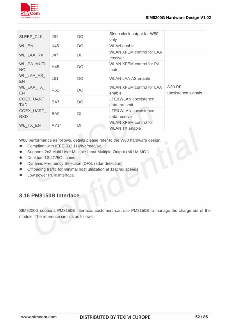
SIM8200G Hardware Design V1.02
www.simcom.com 52 / 85
SLEEP_CLK J51 DO Sleep clock output for W80 only
WL_EN K45 DO WLAN enable
WL_LAA_RX J47 DI WLAN XFEM control for LAA receiver
W80 RF coexistence signals
WL_PA_MUTING
H45 DO WLAN XFEM control for PA mute
WL_LAA_AS_EN
L51 DO WLAN LAA AS enable
WL_LAA_TX_EN
R51 DO WLAN XFEM control for LAA enable
COEX_UART_TXD
BA7 DO LTE&WLAN coexistence data transmit
COEX_UART_RXD
BA9 DI LTE&WLAN coexistence data receive
WL_TX_EN AY14 DI WLAN XFEM control for WLAN TX enable
W80 performance as follows, details please refer to the W80 hardware design. Compliant with IEEE 802.11a/b/g/n/ac/ax. Supports 2x2 Multi-User Multiple-Input Multiple-Output (MU-MIMO.) Dual band 2.4G/5G chains. Dynamic Frequency Selection (DFS, radar detection). Offloading traffic for minimal host utilization at 11ac/ax speeds. Low power PCIe interface.
3.16 PM8150B Interface
SIM8200G supports PM8150B interface, customers can use PM8150B to manage the charge out of the module. The reference circuits as follows:
DISTRIBUTED BY TEXIM EUROPE

SIM8200G Hardware Design V1.02
www.simcom.com 53 / 85
PM8150BModuleSYS_OK_N
FAULT_N
SPMI_CLK
SPMI_DATA
CHG_SYS_OK
FAULT_N
SPMI_CLK
SPMI_DATA
L10E_3P1
VIO_OUT
L10E_3P1
VIO_OUT
1uF1uF
Figure 32: PM8150B interface diagram circuit Table 36: Definition of PM8150B interface Pin name Pin no. Pin characteristics Functional description Comment
CHG_SYS_OK
C43 DI When charger input is inserted PM8150B output signal to PMU
Used for PM8150B only
FAULT_N B44 DIO Used to send/receive the fault condition across all PMICs in the chipset
SPMI_CLK A47 DO SPMI communication bus clock signal Required 50Ω
impedance SPMI_DATA B46 DIO
SPMI communication bus data signal
L10E_3P1 C41 PO Output power supply for PM8150B USB PD-PHY and USB switch
Only used for PM8150B
VIO_OUT D42 PO Output power for PM8150B IO circuit
PM8150B performance as follows: please refer to SIM8200G reference design for details Supports USB Type-C specification Rev. 1.3 and USB power delivery specification Rev. 3.0*. Supports Qualcomm Quick Charge 2.0, Quick Charge 3.0*, and Quick Charge 4.0* technology.
“*” means under development. SPMI interface layout guidelines: Require trace impedance is 50Ω ± 10%.
NOTE
DISTRIBUTED BY TEXIM EUROPE
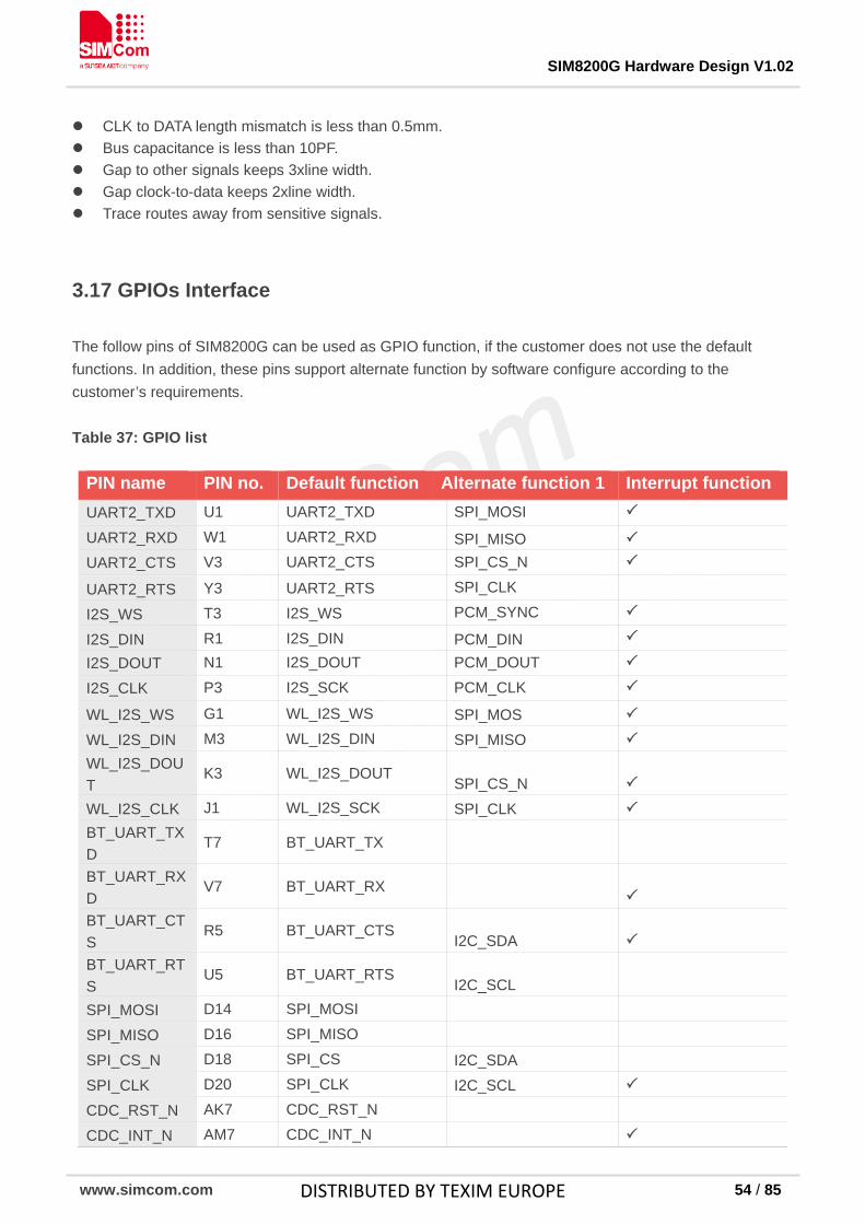
SIM8200G Hardware Design V1.02
www.simcom.com 54 / 85
CLK to DATA length mismatch is less than 0.5mm. Bus capacitance is less than 10PF. Gap to other signals keeps 3xline width. Gap clock-to-data keeps 2xline width. Trace routes away from sensitive signals.
3.17 GPIOs Interface
The follow pins of SIM8200G can be used as GPIO function, if the customer does not use the default functions. In addition, these pins support alternate function by software configure according to the customer’s requirements. Table 37: GPIO list
PIN name PIN no. Default function Alternate function 1 Interrupt function UART2_TXD U1 UART2_TXD SPI_MOSI
UART2_RXD W1 UART2_RXD SPI_MISO
UART2_CTS V3 UART2_CTS SPI_CS_N
UART2_RTS Y3 UART2_RTS SPI_CLK
I2S_WS T3 I2S_WS PCM_SYNC
I2S_DIN R1 I2S_DIN PCM_DIN
I2S_DOUT N1 I2S_DOUT PCM_DOUT
I2S_CLK P3 I2S_SCK PCM_CLK
WL_I2S_WS G1 WL_I2S_WS SPI_MOS
WL_I2S_DIN M3 WL_I2S_DIN SPI_MISO
WL_I2S_DOUT
K3 WL_I2S_DOUT SPI_CS_N
WL_I2S_CLK J1 WL_I2S_SCK SPI_CLK
BT_UART_TXD
T7 BT_UART_TX
BT_UART_RXD
V7 BT_UART_RX
BT_UART_CTS
R5 BT_UART_CTS I2C_SDA
BT_UART_RTS
U5 BT_UART_RTS I2C_SCL
SPI_MOSI D14 SPI_MOSI
SPI_MISO D16 SPI_MISO
SPI_CS_N D18 SPI_CS I2C_SDA
SPI_CLK D20 SPI_CLK I2C_SCL
CDC_RST_N AK7 CDC_RST_N
CDC_INT_N AM7 CDC_INT_N
DISTRIBUTED BY TEXIM EUROPE

SIM8200G Hardware Design V1.02
www.simcom.com 55 / 85
3.18 Network Status The NET_STATUS pin is used to control network status LED, its reference circuit is shown in the following figure.
Module
R1
VCC
NET_STATUS
Q1
Figure 33: NET_STATUS reference circuit Table 38: Definition of NET_STATUS pin
Pin Name Pin No. Electrical Description Description Comments
NET_STATUS AE1 DO Indicate network activity status of the module
1. The value of the resistor R1 depends on the LED characteristics. The timing parameters are shown in the following table. Table 39: NET_STATUS pin status NET_STATUS pin status Module status Always On Searching network; call connection(including 5G,VOLTE) 100ms ON, 100ms OFF Data transmitting; 5G registered on network 200ms ON, 200ms OFF Data transmitting; 4G registered on network 800ms ON, 800ms OFF Data transmitting; 3G registered on network OFF Power off ; in sleep mode
NOTE
DISTRIBUTED BY TEXIM EUROPE

SIM8200G Hardware Design V1.02
www.simcom.com 56 / 85
3.19 Flight Mode Control* The W_DISABLE pin can be used to control SIM8200G to enter or exit the flight mode. In flight mode, the RF circuit is closed to prevent interference with other equipment’s and minimize current consumption. Its reference circuit is shown in the following figure.
ModuleVDD_EXT
10K
HOSTW_DISABLE
Figure 34: W_DISABLE pin reference circuit Table 40: Definition of W_DISABLE pin
Pin Name Pin No. Electrical Description Description Comments
W_DISABLE AG1 DI Flight mode control input active low
Table 41: W_DISABLE pin status W_DISABLE pin status Module operation Input low level Flight mode: RF is disabled
Input high level AT+CFUN=4: Flight mode AT+CFUN=1: RF is enabled (Default)
“*” means under development.
3.20 Antenna Control Interface* ANT_CTL[0:1] and RFFE0 signals are used for tunable antenna control and should be routed to
NOTE
DISTRIBUTED BY TEXIM EUROPE

SIM8200G Hardware Design V1.02
www.simcom.com 57 / 85
anappropriate antenna control circuitry. The following table are the definitions for antenn control interfaces.
Table 42: Definition of antenna control interface through GPIOs
Pin Name Pin No. Electrical Description Description Comments
RFFE0_CLK BA11 DO Antenna tuner MIPI CLK
1.8V voltage domain. If unused, please keep open
RFFE0_DATA BA13 DIO Antenna tuner MIPI DATA
ANT_CTRL0 BA15 DO Antenna tuner control0
ANT_CTRL1 AY16 DO Antenna tuner control1
*: means under development, for details please contact SIMCom support teams. 1. The RFFE0 signals are multiplexed with ANTCTL2 and ANTCTL3.
NOTE
DISTRIBUTED BY TEXIM EUROPE

SIM8200G Hardware Design V1.02
www.simcom.com 58 / 85
4. Antenna Interfaces
SIM8200G provides eight antennas for 3G/4G/5G and GNSS. The antenna ports have an RF impedance of 50Ω.
4.1 Antenna Definitions The detail designs about ANT please refer to the antenna design guide “SIM8200G_LGA Antenna Port Mapping and Design Guide”. Table 43: Antenna port definitions
FUNCTIONS ANTENNAS
ANT0 ANT1 ANT2 ANT3 ANT4 ANT5 ANT6 ANT7
3G/4G/5G LB/MHB TRX1
5G n41 UL/DL-MIMO1
5G n79 DL-MIMO2
4G MHB DL-MIMO2
5G n41/n77/n78 DIV
3G/4G/5G LB/MHB DIV
5G n41/n77/n78 DL-MIMO2
5G n79 UL/DL-MIMO1
3G/4G/5G MHB DL-MIMO1
5G n41 TRX
5G n77/n78 UL/DL-MIMO1
4G UHB UL/DL-MIMO1
5G n77/n78 TRX
4G UHB TRX
5G n79 DRX
GNSS
5G n79 TRX
DISTRIBUTED BY TEXIM EUROPE

SIM8200G Hardware Design V1.02
www.simcom.com 59 / 85
4.1.1 3G/4G/5G Operating Frequency
Table 44: SIM8200G operating frequencies Frequency band Uplink (UL) Downlink (DL) Duplex
mode WCDMA B1 1920 MHz ~1980 MHz 2110 MHz ~2170 MHz FDD
WCDMA B2 1850 MHz ~1910 MHz 1930 MHz ~1990 MHz FDD
WCDMA B3 1710 MHz ~1785 MHz 1805 MHz ~1880 MHz FDD
WCDMA B4 1710 MHz ~1755 MHz 2110 MHz ~ 2155 MHz FDD
WCDMA B5 824 MHz~849 MHz 869 MHz~894MHz FDD
WCDMA B8 880 MHz ~915 MHz 925 MHz ~960 MHz FDD
LTE B1 1920 MHz ~1980 MHz 2110 MHz ~2170 MHz FDD
LTE B2 1850 MHz ~1910MHz 1930 MHz ~1990MHz FDD
LTE B3 1710 MHz ~1785 MHz 1805 MHz ~1880 MHz FDD
LTE B4 1710 MHz ~1755MHz 2110 MHz ~2155MHz FDD
LTE B5 824 MHz~849 MHz 869 MHz~894MHz FDD
LTE B7 2500 MHz ~2570MHz 2620 MHz ~2690MHz FDD
LTE B8 880 MHz ~915 MHz 925 MHz ~960 MHz FDD
LTE B12 699 MHz ~716MHz 729 MHz ~746MHz FDD
LTE B13 777 MHz ~787MHz 746 MHz ~756MHz FDD
LTE B14 788 MHz ~798MHz 758 MHz ~768MHz FDD
LTE B17 704 MHz ~716MHz 734 MHz ~746MHz FDD
LTE B18 815 MHz ~830MHz 860 MHz ~875MHz FDD
LTE B19 830 MHz ~845MHz 875 MHz ~890MHz FDD
LTE B20 832 MHz ~862MHz 791 MHz ~ 821MHz FDD
LTE B25 1850 MHz ~1915MHz 1930 MHz ~1995MHz FDD
LTE B26 814 MHz ~849MHz 859 MHz ~894MHz FDD
LTE B28 703 MHz ~748MHz 758 MHz ~803MHz FDD
LTE B29 / 717 MHz ~728MHz FDD
LTE B30 230 MHz 5~2315MHz 2350 MHz ~2360MHz FDD
LTE B32 / 1452 MHz ~1496MHz FDD
LTE B34 2010 MHz ~2025MHz 2010 MHz ~2025MHz TDD
LTE B38 2570 MHz ~2620 MHz 2570 MHz ~2620 MHz TDD
LTE B39 1880 MHz ~1920MHz 1880 MHz ~1920MHz TDD
LTE B40 2300 MHz ~2400 MHz 2300 MHz ~2400 MHz TDD
LTE B41 2496 MHz ~2690 MHz 2496 MHz ~2690 MHz TDD
LTE B42 340 MHz 0~3600MHz 3400 MHz ~3600MHz TDD
LTE B48 3550 MHz ~3700MHz 3550 MHz ~3700MHz TDD
LTE B66 1710 MHz ~1780MHz 2110 MHz ~2180MHz FDD
LTE B71 663 MHz ~698MHz 61 MHz 7~652MHz FDD
DISTRIBUTED BY TEXIM EUROPE

SIM8200G Hardware Design V1.02
www.simcom.com 60 / 85
LTE-FDD B29 and B32 support Rx only and are only for secondary component carrier. Table 45: NR band
4.12 GNSS Frequency
The following table shows frequency specification of GNSS antenna interface. Table 46: GNSS frequency
Type Frequecy GPS L1/Galileo/QZSS 1575.42±1.023MHz
GPS L5 1176.45±10.23MHz
GLONASS 1597.5~1605.8MHz
BeiDou/Compass 1561.098±2.046MHz
Frequency band Uplink (UL) Downlink (DL) Duplex
mode NR n1 1920 MHz ~1980 MHz 2110 MHz ~2170 MHz FDD
NR n2 1850 MHz ~1910MHz 1930 MHz ~1990MHz FDD
NR n3 1710 MHz ~1785 MHz 1805 MHz ~1880 MHz FDD
NR n5 824 MHz~849 MHz 869 MHz~894MHz FDD
NR n7 250 MHz 0~2570MHz 2620 MHz ~2690MHz FDD
NR n8 880 MHz ~915 MHz 92 MHz 5 ~960 MHz FDD
NR n12 699 MHz ~716MHz 72 MHz 9~746MHz FDD
NR n20 832 MHz ~862MHz 791 MHz ~ 821MHz FDD
NR n25 1850 MHz ~1915MHz 1930 MHz ~1995MHz FDD
NR n28 70 MHz 3~748MHz 758 MHz ~803MHz FDD
NR n40 2300 MHz ~2400 MHz 2300 MHz ~2400 MHz TDD
NR n41 2496 MHz ~2690 MHz 2496 MHz ~2690 MHz TDD
NR n66 1710 MHz – 1780 MHz 2110 MHz – 2200 MHz FDD
NR n71 663 MHz – 698 MHz 617 MHz – 652 MHz FDD
NR n77 3300 MHz – 4200 MHz 3300 MHz – 4200 MHz TDD
NR n78 3300 MHz – 3800 MHz 3300 MHz – 3800 MHz TDD
NR n79 4400 MHz – 5000 MHz 4400 MHz – 5000 MHz TDD
NOTE
DISTRIBUTED BY TEXIM EUROPE

SIM8200G Hardware Design V1.02
www.simcom.com 61 / 85
4.2 Antenna Installation
4.2.1 PCB Layout Guidelines
To avoid interference, minimalize the insertion loss of the RF trace, the PCB should follow below rules: (1) The coaxial cable PCB pads, RF antenna connector and other connectors which used to test
contact performance of module should place as close as to the module antenna pads. (2) The antenna matching network should place to antenna feed port. (3) The RF trace should be as short and straight as possible, and do not routing as perpendicular line,
we recommend do it as 45° corner trace.
(4) And the RF trace ground should be complete; (5) RF device should place ground to the nearest ground plane; (6) Between RF trace and below should avoid other signal trace or parallel trace to the RF signal. (7) Recommend to more ground vias near the RF traces.
4.2.2 Antenna Requirements
The following table shows the requirements on 3G/4G/5G antennas and GNSS antenna. Table 47: 3G/4G/5G/GNSS antennas
Parameter Requirement Operating Frequency See Table 48 for each antenna Direction Omni Directional Gain > -3dBi (Avg) Impedance 50 Ω Efficiency > 50 % Max. Input Power 50W VSWR < 2 Isolation 20dB is preferred Cable Insertion Loss <1GHz <1dB Cable Insertion Loss 1GHz~2.2GHz <1.5dB Cable Insertion Loss 2.3GHz~2.7GHz <2dB Cable Insertion Loss 3.3GHz~6GHz <2.5dB Table 48: GNSS antenna (for dedicated GNSS antenna only)* Parameter Requirement
Operating Frequency L1: 1559~1609MHZ
L5: 1166~1187MHz Direction Hemisphere, face to sky
DISTRIBUTED BY TEXIM EUROPE
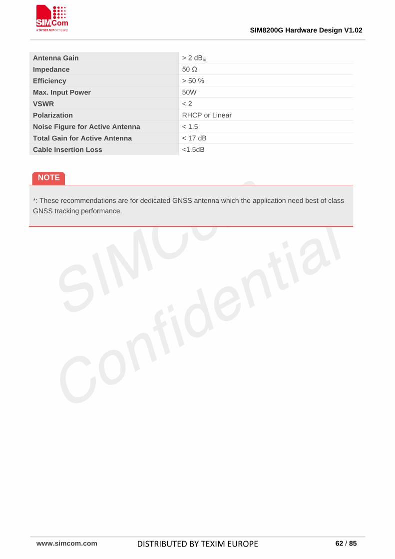
SIM8200G Hardware Design V1.02
www.simcom.com 62 / 85
Antenna Gain > 2 dBic Impedance 50 Ω Efficiency > 50 % Max. Input Power 50W VSWR < 2 Polarization RHCP or Linear Noise Figure for Active Antenna < 1.5 Total Gain for Active Antenna < 17 dB Cable Insertion Loss <1.5dB
*: These recommendations are for dedicated GNSS antenna which the application need best of class GNSS tracking performance.
NOTE
DISTRIBUTED BY TEXIM EUROPE

SIM8200G Hardware Design V1.02
www.simcom.com 63 / 85
5. Electrical Specifications
5.1 Absolute Maximum Ratings
Absolute maximum rating for digital and analog pins of module are listed in the following table: Table 49: Absolute maximum ratings
Parameter Min. Typ. Max. Unit Voltage at VBAT1 pins - - 4.8 V
Voltage at USB_VBUS - - 6 V
Voltage at PWRKEY - - 2.1 V
Voltage at RESIN_N - - 1.9 V
Voltage at digital pins (GPIO,I2C,UART, I2S) - - 2.1 V Voltage at digital pins (U)SIM - - 3.05 V
1. The VBAT include VBAT_BB and VBAT_RF pins.
5.2 Operating Conditions Table 50: VBAT recommended operating ratings Parameter Min. Typ. Max. Unit Voltage at VBAT1 pins 3.3 3.8 4.4 V
1. The VBAT include VBAT_BB and VBAT_RF pins.
NOTE
NOTE
DISTRIBUTED BY TEXIM EUROPE

SIM8200G Hardware Design V1.02
www.simcom.com 64 / 85
Table 51: 1.8V digital I/O characteristics
Parameter Description Min. Typ. Max. Unit VIH High-level input voltage 1.17 - 2.1 V
VIL Low-level input voltage 0 - 0.63 V
VOH High-level output voltage 1.35 - 1.8 V
VOL Low-level output voltage 0 - 0.45 V
IOZH High-level, tri-state leakage current
(no pull down resistor) - - 1 uA
IOZL Low-level, tri-state leakage current (no pull up resistor)
-1 - - uA
IIH Input high leakage current (no pull down resistor) - - 1 uA
IIL Input low leakage current(no pull up resistor) -1 - - uA
These parameters are for digital interface pins, such as UART, I2C, I2S, SPI, and GPIOs (SIM_DET, SD_DET). Table 52: Operating temperature Parameter Min. Typ. Max. Unit Normal operation temperature(3GPP compliant) -30 - 70 ℃
Extended operation temperature -40 - 85 ℃
Storage temperature -40 - 90 ℃
5.3 Operating Mode
5.3.1 Operating Mode Definition
The table below summarizes the various operating modes of module. Table 53: Operating mode definition
Mode Function
Normal operation
UMTS/LTE/5G Sleep
AT command “AT+CSCLK=1” can be used to set the module to a sleep mode. In this case, the current consumption of module will be reduced to a very low level and the module can still receive paging message
NOTE
DISTRIBUTED BY TEXIM EUROPE

SIM8200G Hardware Design V1.02
www.simcom.com 65 / 85
and SMS.
UMTS/LTE/5G Idle
Software is active. Module is registered to the network and ready to communicate.
UMTS/LTE/5G Talk
Connection between two subscribers is in progress. In this case, the power consumption depends on network settings such as DTX off/on, FR/EFR/HR, hopping sequences and antenna.
UMTS/LTE/5G Standby
Module is ready for data transmission, but no data is currently sent or received. In this case, power consumption depends on network settings.
UMTS/LTE/5G Data transmission
There is data transmission in progress. In this case, power consumption is related to network settings (e.g. power control level); uplink/downlink data rates, etc.
Minimum functionality mode
AT command “AT+CFUN=0” can be used to set the Module to a minimum functionality mode without removing the power supply. In this mode, the RF part of the Module will not work and the (U)SIM card will not be accessible, but the serial port and USB port are still accessible. The power consumption in this mode is lower than normal mode.
Flight mode
AT command “AT+CFUN=4” or pulling down the W_disable1# pin can be used to set the Module to flight mode without removing the power supply. In this mode, the RF part of the Module will not work, but the serial port and USB port are still accessible. The power consumption in this mode is lower than normal mode.
Power off
Normally module will go into power off mode by sending the AT command “AT+CPOF” or pull down the FUL_CARD_POWER_OFF# pin. In this mode the power management unit shuts down the power supply, and software is not active. The serial port and USB are is not accessible.
5.3.2 Sleep Mode
In sleep mode, the current consumption of module will be reduced to a very low level. Several hardware and software conditions must be satisfied in order to let module enter into sleep mode: 1. UART condition 2. USB condition 3. Software condition
Before designing, pay attention to how to realize sleeping/waking function. 5.3.3 Minimum Functionality Mode and Flight Mode
Minimum functionality mode ceases a majority function of Module, in order to minimizing the power
NOTE
DISTRIBUTED BY TEXIM EUROPE

SIM8200G Hardware Design V1.02
www.simcom.com 66 / 85
consumption. This mode is set by the AT command which provides a choice of 3 different functionality levels. ● AT+CFUN=0: Minimum functionality ● AT+CFUN=1: Full functionality (Default) ● AT+CFUN=4: Flight mode If module has been set to minimum functionality mode, the RF (U)SIM card function will be closed while the serial port and USB are still available. If module has been set to flight mode, the RF function will be closed, while the (U)SIM card , the serial port and USB are still available. When module is in minimum functionality or flight mode, it can return to full functionality by the AT command “AT+CFUN=1”.
5.4 Current Consumption
The current consumptions are listed in the follows table. Table 54: Current consumption on VBAT pins (VBAT1=3.8V)
GNSS GNSS supply current (AT+CFUN=0,with USB connection)
@ -140dBm,Tracking Typical:TBD
UMTS sleep/idle mode WCDMA supply current (GNSS off, without USB connection)
Sleep mode @DRX=9 Typical: TBD Idle mode @DRX=9 Typical: TBD
LTE sleep/idle mode LTE FDD supply current (GNSS off, without USB connection)
Sleep mode Typical: TBD Idle mode Typical: TBD
LTE TDD supply current (GNSS off, without USB connection)
Sleep mode Typical: TBD Idle mode Typical: TBD
UMTS Talk WCDMA B1 @Power 23dBm Typical: TBD
WCDMA B2 @Power 23dBm Typical: TBD
WCDMA B3 @Power 23dBm Typical: TBD
WCDMA B4 @Power 23dBm Typical: TBD
WCDMA B5 @Power 23dBm Typical: TBD
WCDMA B8 @Power 23dBm Typical: TBD HSDPA data WCDMA B1 @Power 23dBm Typical: TBD
WCDMA B2 @Power 23dBm Typical: TBD
DISTRIBUTED BY TEXIM EUROPE

SIM8200G Hardware Design V1.02
www.simcom.com 67 / 85
WCDMA B3 @Power 23dBm Typical: TBD
WCDMA B4 @Power 23dBm Typical: TBD
WCDMA B5 @Power 23dBm Typical: TBD
WCDMA B8 @Power 23dBm Typical: TBD LTE data
LTE-FDD B1 @5Mbps 23.0dBm Typical: TBD @10Mbps 23.0dBm Typical: TBD @20Mbps 23.0dBm Typical: TBD
LTE-FDD B2 @5Mbps 23.0dBm Typical: TBD @10Mbps 23.0dBm Typical: TBD @20Mbps 23.0dBm Typical: TBD
LTE-FDD B3 @1.5Mbps 23.0dBm Typical: TBD @10Mbps 23.0dBm Typical: TBD @20Mbps 23.0dBm Typical: TBD
LTE-FDD B4 @5Mbps 23.0dBm Typical: TBD @10Mbps 23.0dBm Typical: TBD @20Mbps 23.0dBm Typical: TBD
LTE-FDD B5 @1.5Mbps 23.0dBm Typical: TBD @5Mbps 23.0dBm Typical: TBD @10Mbps 23.0dBm Typical: TBD
LTE-FDD B7 @5Mbps 23.0dBm Typical: TBD @10Mbps 23.0dBm Typical: TBD @20Mbps 23.0dBm Typical: TBD
LTE-FDD B8 @5Mbps 23.0dBm Typical: TBD @10Mbps 23.0dBm Typical: TBD
LTE-FDD B12 @5Mbps 23.0dBm Typical: TBD @10Mbps 23.0dBm Typical: TBD
LTE-FDD B13 @5Mbps 23.0dBm Typical: TBD @10Mbps 23.0dBm Typical: TBD
LTE-FDD B14 @5Mbps 23.0dBm Typical: TBD @10Mbps 23.0dBm Typical: TBD
LTE-FDD B17 @5Mbps 23.0dBm Typical: TBD @10Mbps 23.0dBm Typical: TBD
LTE-FDD B18 @5Mbps 23.0dBm Typical: TBD @10Mbps 23.0dBm Typical: TBD
LTE-FDD B19 @5Mbps 23.0dBm Typical: TBD @10Mbps 23.0dBm Typical: TBD
LTE-FDD B20 @5Mbps 23.0dBm Typical: TBD @10Mbps 23.0dBm Typical: TBD @20Mbps 23.0dBm Typical: TBD
LTE-FDD B25 @5Mbps 23.0dBm Typical: TBD @10Mbps 23.0dBm Typical: TBD
LTE-FDD B26 @5Mbps 23.0dBm Typical: TBD @10Mbps 23.0dBm Typical: TBD
LTE-FDD B28 @5Mbps 23.0dBm Typical: TBD @10Mbps 23.0dBm Typical: TBD
LTE-FDD B30 @5Mbps 23.0dBm Typical: TBD @10Mbps 23.0dBm Typical: TBD
LTE-FDD B34 @5Mbps 23.0dBm Typical: TBD @10Mbps 23.0dBm Typical: TBD
LTE-FDD B38 @5Mbps 23.0dBm Typical: TBD @10Mbps 23.0dBm Typical: TBD
LTE-FDD B39 @5Mbps 23.0dBm Typical: TBD @10Mbps 23.0dBm Typical: TBD
LTE-FDD B40 @5Mbps 23.0dBm Typical: TBD @10Mbps 23.0dBm Typical: TBD
DISTRIBUTED BY TEXIM EUROPE

SIM8200G Hardware Design V1.02
www.simcom.com 68 / 85
NR data 5G n1 @Power 23dBm Typical: TBD 5G n2 @Power 23dBm Typical: TBD 5G n3 @Power 23dBm Typical: TBD 5G n5 @Power 23dBm Typical: TBD 5G n7 @Power 23dBm Typical: TBD 5G n8 @Power 23dBm Typical: TBD 5G n12 @Power 23dBm Typical: TBD 5G n20 @Power 23dBm Typical: TBD 5G n25 @Power 23dBm Typical: TBD 5G n28 @Power 23dBm Typical: TBD 5G n40 @Power 23dBm Typical: TBD 5G n41 @Power 23dBm Typical: TBD 5G n66 @Power 23dBm Typical: TBD 5G n71 @Power 23dBm Typical: TBD 5G n77 @Power 23dBm Typical: TBD 5G n78 @Power 23dBm Typical: TBD 5G n79 @Power 23dBm Typical: TBD
1. The VBAT include VBAT_BB and VBAT_RF pins.
5.5 RF Output Power
The RF output power is shown in the following table. Table 55: Conducted output power
LTE-FDD B41 @5Mbps 23.0dBm Typical: TBD @10Mbps 23.0dBm Typical: TBD
LTE-FDD B42 @5Mbps 23.0dBm Typical: TBD @10Mbps 23.0dBm Typical: TBD
LTE-FDD B48 @5Mbps 23.0dBm Typical: TBD @10Mbps 23.0dBm Typical: TBD
LTE-TDD B66 @5Mbps 23.0dBm Typical : TBD @10Mbps 23.0dBm Typical : TBD @20Mbps 23.0dBm Typical : TBD
LTE-TDD B71 @5Mbps 22.9dBm Typical : TBD @10Mbps 23.0dBm Typical : TBD @20Mbps 23.0dBm Typical : TBD
NOTE
DISTRIBUTED BY TEXIM EUROPE

SIM8200G Hardware Design V1.02
www.simcom.com 69 / 85
Frequency Max Min WCDMA Bands 24dBm + 1/-3dB < -50dBm
LTE-FDD Bands 23dBm + 2/-2dB < -40dBm
LTE-TDD Bands 23dBm + 2/-2dB < -40dBm
NR Bands 23dBm + 2/-3dB < -40dBm
5.6 Conducted Receive Sensitivity
SIM8200G conducted RF receiving sensitivity is fully meet 3GPP specification. Customers can get more details by check 3GPP official website http://www.3gpp.org/.
5.7 Thermal Design
Make sure that the SIM8200G can reach maximum work performance under extended temperature or extreme conditions for a long time, thermal dissipation design is very important.
There are some design rules to enhance thermal dissipation performance: Keep the module away from other heat sources such as battery, power, AP, etc. All the GND pins of the module should be connected. Add enough through GND via on the main PCB. Via material is very important solid copper and
stacked via is better. Make sure maximize airflow around the module. Recommend use heat dissipation material connect to the customers’ device on the top side of the
module to enhance the heat dissipation. Large heat dissipation area is better. Chose a high effective heat dissipation material is better such as heat pipe, graphite sheets.
5.8 ESD Module is sensitive to ESD in the process of storage, transporting, and assembling. When module is mounted on the customers’ main board, the ESD components should be placed closed to the connectors which human body may touch, such as (U)SIM card socket, SD card socket, audio jacks, switches, USB interface, etc. The following table shows the module ESD measurement performance. Table 56: The ESD performance measurement table (temperature: 25 ℃, humidity: 45%) Part Contact discharge Air discharge VBAT,GND ± 5kV ± 10 kV
Antenna ± 5 kV ± 10 kV
PWRKEY ± 4 kV ± 8 kV
DISTRIBUTED BY TEXIM EUROPE

SIM8200G Hardware Design V1.02
www.simcom.com 70 / 85
USB ± 4 kV ± 8 kV
RESET_N ± 3 kV ± 6 kV
(U)SIM ± 3 kV ± 6 kV
Other PADs ±3 kV ±6 kV
Test conditions: the external of the module has surge protection diodes and ESD protection diodes
NOTE
DISTRIBUTED BY TEXIM EUROPE
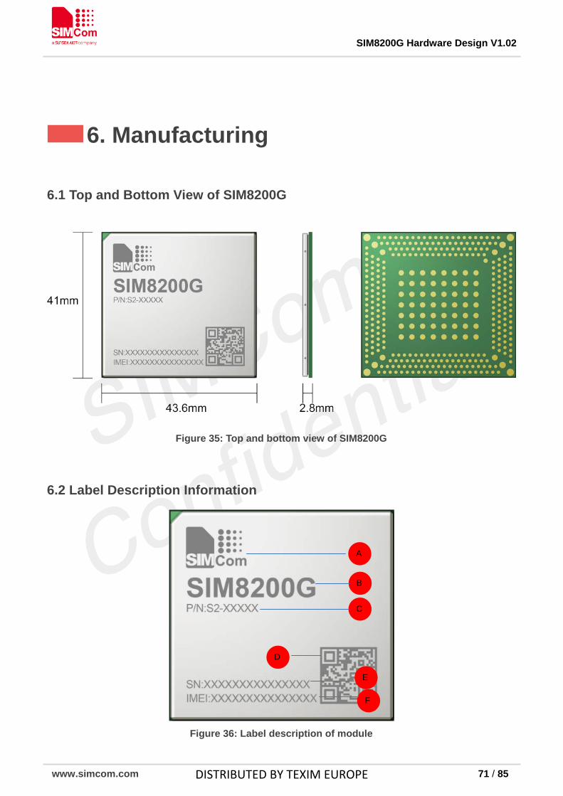
SIM8200G Hardware Design V1.02
www.simcom.com 71 / 85
6. Manufacturing
6.1 Top and Bottom View of SIM8200G
Figure 35: Top and bottom view of SIM8200G
6.2 Label Description Information
Figure 36: Label description of module
E
A
B
C
F
D
DISTRIBUTED BY TEXIM EUROPE

SIM8200G Hardware Design V1.02
www.simcom.com 72 / 85
Table 57: Label description of module information
No. Description A LOGO
B Project name
C Product code
D QR code
E Serial number
F International mobile equipment identity
DISTRIBUTED BY TEXIM EUROPE

SIM8200G Hardware Design V1.02
www.simcom.com 73 / 85
6.3 Recommended PCB Footprint
The following figure shows the PCB footprint of SIM8200G.
Figure 37: Recommended PCB footprint
DISTRIBUTED BY TEXIM EUROPE
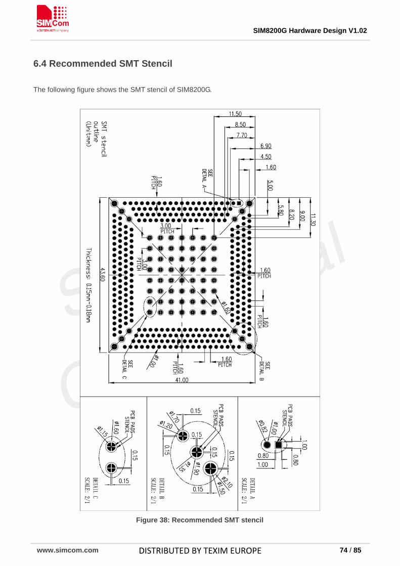
SIM8200G Hardware Design V1.02
www.simcom.com 74 / 85
6.4 Recommended SMT Stencil
The following figure shows the SMT stencil of SIM8200G.
Figure 38: Recommended SMT stencil
DISTRIBUTED BY TEXIM EUROPE

SIM8200G Hardware Design V1.02
www.simcom.com 75 / 85
6.5 Recommended SMT Reflow Profile
The following figure shows the SMT reflow profile of SIM8200G.
Figure 39: Recommended SMT reflow profile
Refer to “Module secondary-SMT-UGD” for more information about the module shipping and manufacturing.
NOTE
DISTRIBUTED BY TEXIM EUROPE

SIM8200G Hardware Design V1.02
www.simcom.com 76 / 85
6.6 Moisture Sensitivity Level (MSL)
SIM8200G is susceptible to damage induced by absorbed moisture and high temperature. A package’s moisture-sensitivity level (MSL) indicates its ability to withstand exposure after it is removed from its shipment bag, while it is on the factory floor awaiting PCB installation. A low MSL rating is better than a high rating; a low MSL device can be exposed on the factory floor longer than a high MSL device. All pertinent MSL ratings are summarized in Table 54. Table 58: MSL ratings summary
MSL Out-of-bag floor life Comments 1 Unlimited ≤+30℃/85% RH
2 1 year ≤+30℃/60% RH
2a 4 weeks ≤+30℃/60% RH
3 168 hours ≤+30℃/60% RH
4 72 hours ≤+30℃/60% RH
5 48 hours ≤+30℃/60% RH
5a 24 hours ≤+30℃/60% RH
6 Mandatory bake before use. After bake, it must be
reflowed within the time limit specified on the label. ≤+30℃/60% RH
The SIM8200G device samples are currently classified as MSL3 at 255 (+5, -0)°C, following the latest IPC/JEDEC J-STD-020 standard revision for moisture-sensitivity qualification This qualification temperature (255°C) should not be confused with the peak temperature within the recommended solder reflow profile.
6.7 Baking Requirements
It is necessary to bake modules if the prescribed time limit has been exceeded. The baking conditions are specified in table 59. Note that if baking is required, the devices must be transferred into trays that can be baked to at least 125°C. Table 59: Baking requirements
Baking conditions options Duration 40°C±5°C, <5% RH 192 hours
120°C±5°C, <5% RH 4 hours
DISTRIBUTED BY TEXIM EUROPE

SIM8200G Hardware Design V1.02
www.simcom.com 77 / 85
7. Packaging
SIM8200G module supports tray packaging. The packaging process is shown in the following figures.
Figure 40: Packaging process Module tray drawing:
Figure 41: Module tray drawing
DISTRIBUTED BY TEXIM EUROPE

SIM8200G Hardware Design V1.02
www.simcom.com 78 / 85
Table 60: Tray size Length(±3mm) Width(±3mm) Number 242.0 161.0 8
Figure 42: Small carton drawing Table 61: Small carton size Length(±10mm) Width(±10mm) Height(±10mm) Number 270 180 120 8*19-2=150 Big carton drawing:
Internal
DISTRIBUTED BY TEXIM EUROPE

SIM8200G Hardware Design V1.02
www.simcom.com 79 / 85
Figure 43: Big carton drawing Table 62: Big carton size Length(±10mm) Width(±10mm) Height(±10mm) Number 380 280 280 150*4=600
Internal
DISTRIBUTED BY TEXIM EUROPE

SIM8200G Hardware Design V1.02
www.simcom.com 80 / 85
8. Appendix
8.1 Coding Schemes and Maximum Net Data Rates over Air Interface
Table 63: Coding schemes and maximum net data rates over air interface HSDPA device category Max data rate(peak) Modulation type Category 1 1.2Mbps 16QAM,QPSK
Category 2 1.2Mbps 16QAM,QPSK
Category 3 1.8Mbps 16QAM,QPSK
Category 4 1.8Mbps 16QAM,QPSK
Category 5 3.6Mbps 16QAM,QPSK
Category 6 3.6Mbps 16QAM,QPSK
Category 7 7.2Mbps 16QAM,QPSK
Category 8 7.2Mbps 16QAM,QPSK
Category 9 10.2Mbps 16QAM,QPSK
Category 10 14.4Mbps 16QAM,QPSK
Category 11 0.9Mbps QPSK
Category 12 1.8Mbps QPSK
Category 13 17.6Mbps 64QAM
Category 14 21.1Mbps 64QAM
Category 15 23.4Mbps 16QAM
Category 16 28Mbps 16QAM
Category 17 23.4Mbps 64QAM
Category 18 28Mbps 64QAM
Category 19 35.5Mbps 64QAM
Category 20 42Mbps 64QAM
Category 21 23.4Mbps 16QAM
Category 22 28Mbps 16QAM
Category 23 35.5Mbps 64QAM
Category 24 42.2Mbps 64QAM
HSUPA device category Max data rate(peak) Modulation type Category 1 0.96Mbps QPSK
Category 2 1.92Mbps QPSK
Category 3 1.92Mbps QPSK
Category 4 3.84Mbps QPSK
DISTRIBUTED BY TEXIM EUROPE

SIM8200G Hardware Design V1.02
www.simcom.com 81 / 85
Category 5 3.84Mbps QPSK
Category 6 5.76Mbps QPSK LTE-FDD device category (Downlink) Max data rate(peak) Modulation type
Category 1 10Mbps QPSK/16QAM/64QAM
Category 2 50Mbps QPSK/16QAM/64QAM
Category 3 100Mbps QPSK/16QAM/64QAM
Category 4 150Mbps QPSK/16QAM/64QAM
Category 5 300Mbps QPSK/16QAM/64QAM
Category 6 300Mbps QPSK/16QAM/64QAM LTE-FDD device category (Uplink) Max data rate(peak) Modulation type
Category 1 5Mbps QPSK/16QAM
Category 2 25Mbps QPSK/16QAM
Category 3 50Mbps QPSK/16QAM
Category 4 50Mbps QPSK/16QAM
Category 5 75Mbps QPSK/16QAM/64QAM
Category 6 50Mbps QPSK/16QAM
DISTRIBUTED BY TEXIM EUROPE

SIM8200G Hardware Design V1.02
www.simcom.com 82 / 85
8.2 Related Documents
Table 64: Related documents NO. Title Description
[1] SIM8200 Series_AT Command Manual AT Command Manual
[2] ITU-T Draft new recommendationV.25ter Serial asynchronous automatic dialing and control
[3] 3GPP TS 51.010-1 Digital cellular telecommunications system (Release 5); Mobile Station (MS) conformance specification
[4] 3GPP TS 34.124 Electromagnetic Compatibility (EMC) for mobile terminals and ancillary equipment.
[5] 3GPP TS 34.121 Electromagnetic Compatibility (EMC) for mobile terminals and ancillary equipment.
[6] 3GPP TS 34.123-1 Technical Specification Group Radio Access Network; Terminal conformance specification; Radio transmission and reception (FDD)
[7] 3GPP TS 34.123-3 User Equipment (UE) conformance specification; Part 3: Abstract Test Suites.
[8] EN 301 908-02 V2.2.1
Electromagnetic compatibility and Radio spectrum Matters (ERM); Base Stations (BS) and User Equipment (UE) for IMT-2000. Third Generation cellular networks; Part 2: Harmonized EN for IMT-2000, CDMA Direct Spread (UTRA FDD) (UE) covering essential requirements of article 3.2 of the R&TTE Directive
[9] EN 301 489-24 V1.2.1
Electromagnetic compatibility and Radio Spectrum Matters (ER Electromagnetic Compatibility (EMC) standard for radio equipm and services; Part 24: Specific conditions for IMT-2000 CDMA Spread (UTRA) for Mobile and portable (UE) radio and ancillary equipment
[10] IEC/EN60950-1(2001) Safety of information technology equipment (2000)
[11] 3GPP TS 51.010-1 Digital cellular telecommunications system (Release 5); Mobile Station (MS) conformance specification
[12] GCF-CC V3.23.1 Global Certification Forum - Certification Criteria
[13] 2002/95/EC Directive of the European Parliament and of the Council of 27 J 2003 on the restriction of the use of certain hazardous substan electrical and electronic equipment (RoHS)
[14] SIM8200 Series_UART_Applicat Note
This document describes how to use UART interface of SIMCo modules.
[15] Antenna design guidelines for div receiver system Antenna design guidelines for diversity receiver system
DISTRIBUTED BY TEXIM EUROPE

SIM8200G Hardware Design V1.02
www.simcom.com 83 / 85
8.3 Terms and Abbreviations
Table 65: Terms and abbreviations Abbreviation Description ADC Analog-to-Digital Converter
CS Coding Scheme
CTS Clear to Send
DRX Discontinuous Reception
DTR Data Terminal Ready
DTX Discontinuous Transmission
EFR Enhanced Full Rate
EMC Electromagnetic Compatibility
ESD Electrostatic Discharge
FDD Frequency Division Dual
FR Full Rate
GNSS Global Navigation Satellite System
GPS Global Positioning System
HR Half Rate
I2C Inter-Integrated Circuit
I2S Inter-IC Sound
IMEI International Mobile Equipment Identity
LTE Long Term Evolution
MDIO Management Data Input/Output
MMD MDIO manageable device
MO Mobile Originated
MSB Most Significant Bit
PCB Printed Circuit Board
PCIe Peripheral Component Interface Express
RF Radio Frequency
RGMII Reduced Gigabit Media Independent Interface
SDIO Secure Digital Input and Output
SIM Subscriber Identification Module
SMS Short Message Service
SPI serial peripheral interface
TDD Time Division Dual
TX Transmit Direction
UART Universal Asynchronous Receiver & Transmitter
VSWR Voltage Standing Wave Ratio
SM SIM phonebook
DISTRIBUTED BY TEXIM EUROPE

SIM8200G Hardware Design V1.02
www.simcom.com 84 / 85
HSDPA High Speed Downlink Packet Access
HSUPA High Speed Uplink Packet Access
WCDMA Wideband Code Division Multiple Access
(U)SIM Universal subscriber identity module
UMTS Universal mobile telecommunications system
UART Universal asynchronous receiver transmitter LB Low Frequency Band MHB Middle and High Frequency Band UHB Ultra High Frequency Band LAA Limited Access Authorization TRX Transmit and Receive signal UL-MIMO Uplink- Multiple Input Multiple Output DL-MIMO Downlink- Multiple Input Multiple Output
DISTRIBUTED BY TEXIM EUROPE
SIM8200G Hardware Design V1.02
www.simcom.com 85 / 85
8.4 Safety Caution
Table 66: Safety caution
Marks Requirements
When in a hospital or other health care facility, observe the restrictions about the use of mobiles. Switch the cellular terminal or mobile off, medical equipment may be sensitive and not operate normally due to RF energy interference.
Switch off the cellular terminal or mobile before boarding an aircraft. Make sure it is switched off. The operation of wireless appliances in an aircraft is forbidden to prevent interference with communication systems. Forgetting to think much of these instructions may impact the flight safety, or offend local legal action, or both.
Do not operate the cellular terminal or mobile in the presence of flammable gases or fumes. Switch off the cellular terminal when you are near petrol stations, fuel depots, chemical plants or where blasting operations are in progress. Operation of any electrical equipment in potentially explosive atmospheres can constitute a safety hazard.
Your cellular terminal or mobile receives and transmits radio frequency energy while switched on. RF interference can occur if it is used close to TV sets, radios, computers or other electric equipment.
Road safety comes first! Do not use a hand-held cellular terminal or mobile when driving a vehicle, unless it is securely mounted in a holder for hands free operation. Before making a call with a hand-held terminal or mobile, park the vehicle.
Mobiles operate over radio frequency signals and cellular networks and cannot be guaranteed to connect in all conditions, especially with a mobile fee or an invalid (U)SIM card. While you are in this condition and need emergent help, please remember to use emergency calls. In order to make or receive calls, the cellular terminal or mobile must be switched on and in a service area with adequate cellular signal strength. Some networks do not allow for emergency call if certain network services or phone features are in use (e.g. lock functions, fixed dialing etc.). You may have to deactivate those features before you can make an emergency call. Also, some networks require that a valid (U)SIM card be properly inserted in the cellular terminal or mobile.
DISTRIBUTED BY TEXIM EUROPE

Contact details
2019 version 1.0
The Netherlands
Germany North
Nordic region
Belgium
Germany South
UK & Ireland
Austria
Elektrostraat 17NL-7483 PG Haaksbergen
T: +31 (0)53 573 33 33F: +31 (0)53 573 33 30E: [email protected]
Bahnhofstrasse 92D-25451 Quickborn
T: +49 (0)4106 627 07-0F: +49 (0)4106 627 07-20E: [email protected]
Sdr. Jagtvej 12DK-2970 Hørsholm
T: +45 88 20 26 30F: +45 88 20 26 39E: [email protected]
Zuiderlaan 14 bus 10B-1731 Zellik
T: +32 (0)2 462 01 00F: +32 (0)2 462 01 25E: [email protected]
Martin-Kollar-Strasse 9D-81829 München
T: +49 (0)89 436 086-0F: +49 (0)89 436 086-19E: [email protected]
St. Mary’s House, Church LaneCarlton Le MoorlandLincoln LN5 9HS
T: +44 (0)1522 789 555F: +44 (0)845 299 22 26E: [email protected]
Warwitzstrasse 9 A-5020 Salzburg
T: +43 (0)662 216 026F: +43 (0)662 216 026-66E: [email protected]
General information
Italy
Via Matteotti 43IT-20864 Agrate Brianza (MB)
T: +39 (0)39 971 3293F: +39 (0)39 971 3293E: [email protected]