note d'etude / technical document - texim europe hilo technical... · note d’étude /...
TRANSCRIPT
page 1/34
____________________________________________________________________________________________
Note d’étude / Technical document : URD1– OTL 5635.1– 005 / 70086 Edition 04
Document Sagem Communications Reproduction et divulgation interdites
Sagem Communications document. Reproduction and disclosure prohibited
Direction des Recherches et des Développements Etablissement de VELIZY
VELIZY R&D Center
NOTE D'ETUDE / TECHNICAL DOCUMENT
REFERENCE
URD1 – OTL 5635.1– 005 /
ETUDE / PROJECT
NOM DE L’ETUDE
70086 Code C TA1 HiLo Module
TITRE / TITLE :
HiLo technical specification
RESUME / SUMMARY
This document is the Hardware specification of the HiLo module.
Mots clés / Keywords : Cellular, module, GSM, GPRS, client
page 2/34
____________________________________________________________________________________________
Note d’étude / Technical document : URD1– OTL 5635.1– 005 / 70086 Edition 04
Document Sagem Communications Reproduction et divulgation interdites
Sagem Communications document. Reproduction and disclosure prohibited

page 3/34
____________________________________________________________________________________________
Note d’étude / Technical document : URD1– OTL 5635.1– 005 / 70086 Edition 04
Document Sagem Communications Reproduction et divulgation interdites
Sagem Communications document. Reproduction and disclosure prohibited
Direction des Recherches et des Développements Etablissement de VELIZY
VELIZY R&D Center
NOTE D'ETUDE / TECHNICAL DOCUMENT
FICHE RECAPITULATIVE / SUMMARY SHEET
Ed Date
Date
Référence
Reference
Pages
modifiées /
Changed
pages
Observations
Comments
1 14/09/2007 URD1– OTL 5635.1–
005 / 70086
Création du document
/ Document creation
2 08/10/2007 URD1– OTL 5635.1–
005 / 70086
Complete review of the
document
3 04/12/2007 URD1– OTL 5635.1–
005 / 70086
Main modifications are
- Dimension changes
- pin allocation change
4 04/02/2008 URD1– OTL 5635.1–
005 / 70086
Electrical signals and
audio pages
- SIM pin numbers,
sec.3.1.1
- Mechanical drawing
5
6
7

page 4/34
____________________________________________________________________________________________
Note d’étude / Technical document : URD1– OTL 5635.1– 005 / 70086 Edition 04
Document Sagem Communications Reproduction et divulgation interdites
Sagem Communications document. Reproduction and disclosure prohibited
Direction des Recherches et des Développements Etablissement de VELIZY
VELIZY R&D Center
SOMMAIRE / CONTENTS
1. INTRODUCTION......................................................................................................................................................7
1.1 PRODUCT CONCEPT ........................................................................................................................................7 1.2 STANDARDS .......................................................................................................................................................7 1.3 TERMS AND ABBREVIATION..........................................................................................................................8 1.4 CONVENTIONS ...................................................................................................................................................9 1.5 PRODUCT FEATURES OVERVIEW................................................................................................................9
2. BLOCK DIAGRAM ................................................................................................................................................11 3. FUNCTIONAL DESCRIPTION ............................................................................................................................12
3.1 SIM .......................................................................................................................................................................12 3.1.1 SIM card interface ....................................................................................................................................12 3.1.2 SIM card connection ...............................................................................................................................12
3.2 AUDIO .................................................................................................................................................................13 3.3 PWM ....................................................................................................................................................................13 3.4 DATA ...................................................................................................................................................................14
3.4.1 Data services.............................................................................................................................................14 3.4.2 UART: V24..................................................................................................................................................14 3.4.3 SPI................................................................................................................................................................14
3.5 ANTENNA...........................................................................................................................................................15 3.5.1 Access ........................................................................................................................................................15 3.5.2 Matching network ....................................................................................................................................15
3.6 SPARE I/O ..........................................................................................................................................................15 3.7 POWER MANAGEMENT .................................................................................................................................16
3.7.1 Power supply ............................................................................................................................................16 3.7.2 VGPIO..........................................................................................................................................................16 3.7.3 VBACKUP...................................................................................................................................................16 3.7.4 Recommended strategy: software management .............................................................................16
3.8 DATA / COMMAND MULTIPLEXING ............................................................................................................16 4. PINOUT ...................................................................................................................................................................18 5. ELECTRICAL SPECIFICATION..........................................................................................................................20
5.1 VBAT ...................................................................................................................................................................20 5.2 VGPIO..................................................................................................................................................................21 5.3 VBACKUP...........................................................................................................................................................21 5.4 VSIM ....................................................................................................................................................................22 5.5 DIGITAL INTERFACE.......................................................................................................................................22 5.6 POK_IN ...............................................................................................................................................................22 5.7 SIM .......................................................................................................................................................................23 5.8 PWM ....................................................................................................................................................................23 5.9 AUX_ADC ...........................................................................................................................................................24
page 5/34
____________________________________________________________________________________________
Note d’étude / Technical document : URD1– OTL 5635.1– 005 / 70086 Edition 04
Document Sagem Communications Reproduction et divulgation interdites
Sagem Communications document. Reproduction and disclosure prohibited
5.10 UART ...............................................................................................................................................................24 5.11 AUDIO SIGNALS ...........................................................................................................................................25
5.11.1 Audio Inputs ..............................................................................................................................................25 5.11.2 Audio Outputs...........................................................................................................................................25
6. ENVIRONMENTAL SPECIFICATION ................................................................................................................26 6.1 NORMAL RANGE, FROM -20°C TO +80°C: ................................................................................................26 6.2 EXTENDED RANGE, FROM -40°C TO -20°C AND FROM +80°C TO +85°C (TBC): ...........................26 6.3 OUT OF OPERATIONAL RANGE:.................................................................................................................26
7. ESD ..........................................................................................................................................................................27 8. MECHANICAL SPECIFICATION ........................................................................................................................28
8.1 PHYSICAL DIMENSIONS ................................................................................................................................28 8.2 ASSEMBLY ........................................................................................................................................................28 8.3 TERMINAL ASSIGNMENTS............................................................................................................................32
8.3.1 Board to Board connection ...................................................................................................................32 8.3.2 Antenna connection ................................................................................................................................33
9. REFERENCE DOCUMENTS ...............................................................................................................................35
page 6/34
____________________________________________________________________________________________
Note d’étude / Technical document : URD1– OTL 5635.1– 005 / 70086 Edition 04
Document Sagem Communications Reproduction et divulgation interdites
Sagem Communications document. Reproduction and disclosure prohibited
1. INTRODUCTION
This document describes the hardware interface of the Sagem HiLo module that connects to the cellular device application and the air interface.
1.1 PRODUCT CONCEPT
The HiLo module is the smallest GPRS (multislot class 10) quad band module of the market with an industrial
connector. The target application is the Machine to Machine market including automotive, AMM (Automatic Metering Management), tracking system, Alarm, etc. Despite its small size and cost, it has comprehensive GSM/GPRS services, data and IP features. In addition to its size it has the following outstanding characteristics:
- High temperature range: -40°C to +85°C - Low power consumption in idle mode: 1.25 mA in DRX5 - Full automotive qualification - High input voltage range: 3.2 V to 4.5 V
As other Sagem GSM/GPRS/EDGE modules, it has a full set of AT commands as well as analogue audio interface. In addition to the HiLo module a complete development kit can be provided to customers including evaluation-board, audio and RF tools.
1.2 STANDARDS This product with its evaluation board has been approved to comply with the directives and standards listed below:
Directives 99/05/EC « Directive of the European Parliament and of the council of 9 March 1999 on radio
equipment and telecommunications terminal equipment and the mutual recognition of their conformity », in short referred to as R&TTE Directive 1999/5/EC
2004/108/EC Directive on electromagnetic compatibility
2006/95/EC « Directive on electrical equipment designed for use within certain voltage limits » (Low Voltage Directive)
2002/95/EC RoHS Directive 95/94/EC Automotive EMC Directive
FCC part 2 Frequency allocations and radio treaty matters FCC part 15 Radio frequency devices subpart B – Unintentional Radiators FCC part 22 Public mobile services subpart H – Cellular Radio Telephone Service FCC part 24 Personal Communications Services, PCS (Narrow band PCS 901-902, 930-931, 940-
941 MHz . Broadband PCS 1850-1990 MHz)
Standards of type approval 3GPP TS 51.010-1 « Digital cellular telecommunications system (Phase 2); Mobile Station (MS)
conformance specification »
page 7/34
____________________________________________________________________________________________
Note d’étude / Technical document : URD1– OTL 5635.1– 005 / 70086 Edition 04
Document Sagem Communications Reproduction et divulgation interdites
Sagem Communications document. Reproduction and disclosure prohibited
ETSI EN 301 511 « Candidate Harmonized European Standard (Telecommunications series) Global System for Mobile communications (GSM); Harmonized standard for mobile stations in the GSM 900 and DCS 1800 bands covering essential requirements under article 3.2 of the R&TTE directive (1999/5/EC) (GSM 13.11 version 7.0.1 Release 1998) »
GCF-CC ver 3.28.0 Global Certification Forum - Certification Criteria
PTCRB ver 3.13.0 PCS Type Certification Review Board ETSI EN 301 489-7 « Candidate Harmonized European Standard (Telecommunications series) Electro
Magnetic Compatibility and Radio spectrum Matters (ERM); Electro Magnetic Compatibility (EMC) standard for radio equipment and services; Part 7: Specific conditions for mobile and portable radio and ancillary equipment of digital cellular radio telecommunications systems (GSM and DCS) »
EN 60 950 Safety of information technology equipment Requirements of quality IEC 60068 Environmental testing
1.3 TERMS AND ABBREVIATION ADC Analog to Digital Converter CODEC Coder-Decoder CTS Clear To Send DCS Digital Communications System DSR Data Set Ready DTR Data Terminal Ready EGSM Enhanced GSM ESD Electrostatic Discharge ETS European Telecommunication Standard GSM Global System for Mobile communication GPRS General Packet Radio Services IC Integrated Circuit IEEE Institute of Electrical and Electronics Engineers I/O Input / Output ISO International Standards Organisation ITU International Telecommunication Union JTAG Joint Test Action Group Kbps Kbits per second LCD Liquid Crystal Display LED Light Emitting Diode Mbps Mbits per second PBCCH Packet Broadcast Channel PCB Printed Circuit Board PCS Personal Communication System PWM Pulse Width Modulation RAM Random Access Memory RF Radio Frequency RI Ring Indication RMS Root Mean Square RTS Ready To Send RX Reception SIM Subscriber Identification Module
page 8/34
____________________________________________________________________________________________
Note d’étude / Technical document : URD1– OTL 5635.1– 005 / 70086 Edition 04
Document Sagem Communications Reproduction et divulgation interdites
Sagem Communications document. Reproduction and disclosure prohibited
SMS Short Message Service TBC To Be Confirmed TBD To Be Defined TX Transmission UART Universal Asynchronous Receiver and Transmitter USSD Unstructured Supplementary Service Data
1.4 CONVENTIONS Throughout this document, DTE (Data Terminal equipment) indicates the equipment which masters and controls the module device HiLo by sending AT commands via its serial interface. DCE (Data Communication Equipment) indicates the module device HiLo.
1.5 PRODUCT FEATURES OVERVIEW Temperature range Normal range: -20°C to +80°C (fully compliant)
Extended range: -40°C to –20°C and +80°C to +85°C (fully functional) Storage: -40°C to +85°C
Weight (in g) 4.3g (typical)
ESD ESD protection < 2 kV
Physical dimensions 27x27x3.6 mm (typical)
Connection 40 pins connector + 1 RF connector + 1 pair of antenna pad
Power supply 3.2V to 4.5V range, 3.7V nominal
Power consumption* Off mode: 56 µA
Stand-by mode: 1.25 mA in DRX5 Communication mode (at Pmax): GSM --- 220 mA DCS --- 160 mA
Battery charge management and interface
No battery charge management is included.
Antenna No antenna is included in the module.
Frequency bands SAGEM module supports GSM850, EGSM900, DCS1800, PCS 1900 (Frequency bands are selectable thanks to AT commands : see document "AT command Set for SAGEM Modules”)
Voice codec Half Rate, Full Rate, Enhanced Full Rate, Adaptive Multi Rate
GSM class Small MS
Transmit power Class 4 (2W) for GSM850 / EGSM900 Class 1 (1W) for DCS1800 / PCS1900
Supported SIM card 3V and 1.8V SIM cards
SIM slot Signals for the management of the SIM card are provided on 40 pins connector
* The power consumption is highly dependent on customer’s product design and environment of GSM Module
page 9/34
____________________________________________________________________________________________
Note d’étude / Technical document : URD1– OTL 5635.1– 005 / 70086 Edition 04
Document Sagem Communications Reproduction et divulgation interdites
Sagem Communications document. Reproduction and disclosure prohibited
PWM Signals for LED, vibrating device and Buzzer management are provided on the PWM interface
Audio up-link 1 single end input is provided for microphone
Audio down-link 1 differential output is provided for non stereo earphone
UART interface with flow control Up to 115.2 Kbps with auto-bauding. Full flow control signals (+2.8V) are provided on 40 pins connector. A reference schematic to build the RS232 interface is provided in the HiLo application note.
Data/command multiplexing Software management of data/command multiplexing on the serial link UART
Data services GPRS, CSD, Fax
Supplementary services (supported via AT commands)
Caller Line Identification, Call Waiting, Call Hold, Call Forwarding, Multiparty, Call Barring, Advice of Charge, USSD, CPHS
Power on pin Available
General purpose I/Os pin 5 GPIO + 1 ADC available
GSM release R99
GPRS SMG 31bis, Multi slot class 10, class B terminal, PBCCH support
GSM/DCS certification GCF-CC V3.28.0
PCS certification NAPRD03 (V3.13.0)
page 10/34
_____________________________________________________________________________________________________________________________________________________________
Note d’étude / Technical document : URD1– OTL 5635.1– 005 / 70086 Edition 04
Document Sagem Communications Reproduction et divulgation interdites
Sagem Communications document. Reproduction and disclosure prohibited
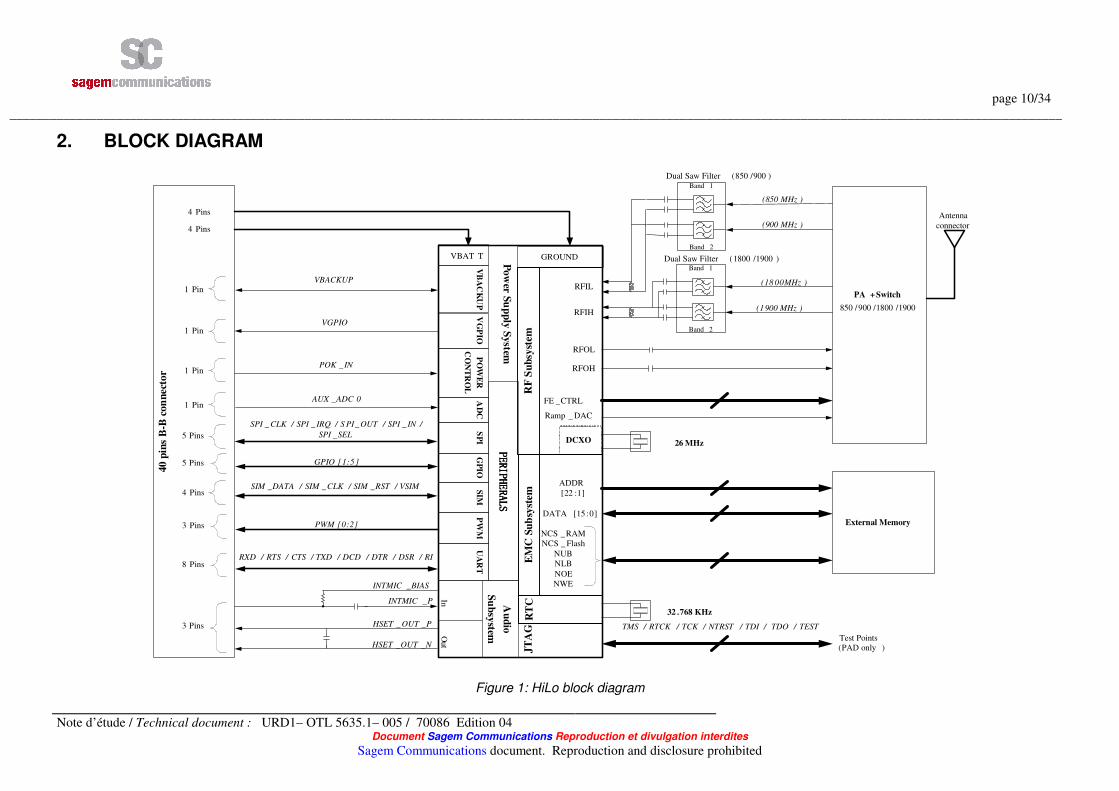
2. BLOCK DIAGRAM
PA +Switch
850 /900 /1800 /1900
(18 00MHz )
(1900 MHz )
RFIL
RFIH
RFOL
RFOH
FE _CTRL
Ramp _ DAC
RF
Su
bsy
stem
DCXO 26 MHz
Antenna
connector
EM
CS
ub
syst
emExternal Memory
ADDR
[22 :1]
DATA [15 :0]
NCS _RAM
NCS _ Flash
NUB
NLB
NOE
NWE
RT
C
32 .768 KHz
AD
CS
PI
40
pin
sB
-Bco
nn
ecto
r
VBAT T
TMS / RTCK / TCK / NTRST / TDI / TDO / TEST
Au
dio
Su
bsy
stemG
PIO
SIM
PW
M
PP PP EE EE RR RR II II PP PP HH HH EE EERR RR AA AA LL LL SS SS
SIM _DATA / SIM _CLK / SIM _RST / VSIM
PWM [0:2]
UA
RT
RXD / RTS / CTS / TXD / DCD / DTR / DSR / RI
InO
ut
SPI _ CLK / SPI _ IRQ / S PI_ OUT / SPI _ IN /
SPI _SEL
INTMIC _BIAS
INTMIC _P
HSET _ OUT _P
HSET _OUT _N
3 Pins
8 Pins
3 Pins
4 Pins
5 Pins
1 Pin
GROUND
4 Pins
4 Pins
JT
AG
Test Points
(PAD only )
AUX _ADC 0
VB
AC
KU
P
Pow
erS
up
ply
System
VG
PIO
PO
WE
R
CO
NT
RO
L
1 Pin
1 Pin
1 Pin
POK _IN
VGPIO
VBACKUP
Band 1
Band 2
Dual Saw Filter (1800 /1900 )
Band 1
Band 2
Dual Saw Filter (850 /900 )
(850 MHz )
(900 MHz )
GPIO [1:5]5 Pins
Figure 1: HiLo block diagram

page 11/34
____________________________________________________________________________________________
Note d’étude / Technical document : URD1– OTL 5635.1– 005 / 70086 Edition 04
Document Sagem Communications Reproduction et divulgation interdites
Sagem Communications document. Reproduction and disclosure prohibited
3. FUNCTIONAL DESCRIPTION
3.1 SIM
3.1.1 SIM card interface
The SIM card interface is compatible with the ISO 7816-3 IC card standard on the issues required by the GSM 11.11 Phase 2+ standard and adapts to 3V and 1.8V SIM card. To prevent SIM card’s damages, the power supply of the module has to be turned off before any manipulation on SIM card. The SIM card interface includes:
- Power supply output (VSIM) - Bi-direction data signal (SIM_DATA), - Clock output (SIM_CLK) - Reset signal (SIM_RST)
Signal Pin N° Description
SIM_RST 15 SIM reset, provided by Base-band processor
SIM_CLK 16 SIM clock, provided by Base-band processor
VSIM 24 SIM supply voltage
SIM_DATA 25 SIM serial data line, input and output
3.1.2 SIM card connection
Figure 2: SIM connection
HiLo
VSIM
SIM_DATA
SIM_RST
SIM_CLK
SIM card
page 12/34
____________________________________________________________________________________________
Note d’étude / Technical document : URD1– OTL 5635.1– 005 / 70086 Edition 04
Document Sagem Communications Reproduction et divulgation interdites
Sagem Communications document. Reproduction and disclosure prohibited
3.2 AUDIO The module supports the following voice codec:
• Half-Rate
• Full-Rate
• Enhanced Full Rate
• Adaptive Multi Rate Signal Pin N° Description
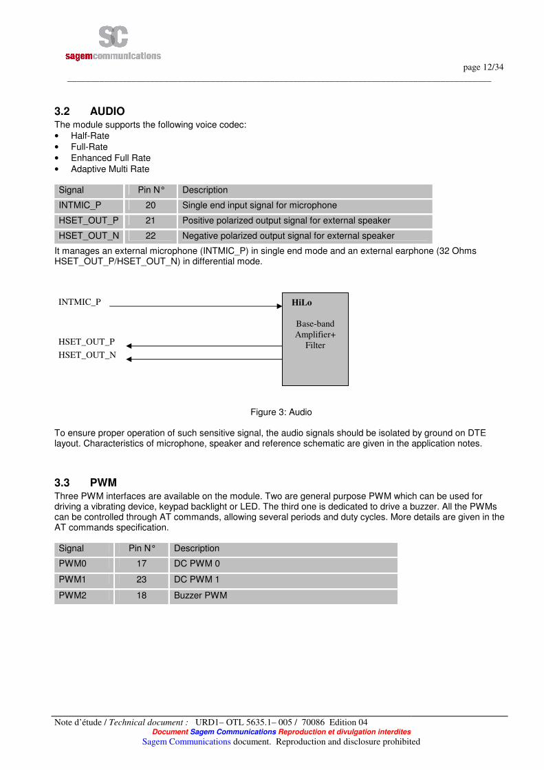
INTMIC_P 20 Single end input signal for microphone
HSET_OUT_P 21 Positive polarized output signal for external speaker
HSET_OUT_N 22 Negative polarized output signal for external speaker
It manages an external microphone (INTMIC_P) in single end mode and an external earphone (32 Ohms HSET_OUT_P/HSET_OUT_N) in differential mode.
Figure 3: Audio
To ensure proper operation of such sensitive signal, the audio signals should be isolated by ground on DTE layout. Characteristics of microphone, speaker and reference schematic are given in the application notes.
3.3 PWM Three PWM interfaces are available on the module. Two are general purpose PWM which can be used for driving a vibrating device, keypad backlight or LED. The third one is dedicated to drive a buzzer. All the PWMs can be controlled through AT commands, allowing several periods and duty cycles. More details are given in the AT commands specification. Signal Pin N° Description
PWM0 17 DC PWM 0
PWM1 23 DC PWM 1
PWM2 18 Buzzer PWM
HiLo
Base-band
Amplifier+
Filter
INTMIC_P
HSET_OUT_P
HSET_OUT_N
page 13/34
____________________________________________________________________________________________
Note d’étude / Technical document : URD1– OTL 5635.1– 005 / 70086 Edition 04
Document Sagem Communications Reproduction et divulgation interdites
Sagem Communications document. Reproduction and disclosure prohibited
3.4 DATA
3.4.1 Data services
The module supports the following services:
• Built-in data / fax Modem
• Data over CSD 9.6 kbps
• Data over GPRS
3.4.2 UART: V24
A V24 interface is provided on external pins of the module with the following signals: - RX/TX - RTS/CTS - DSR - DTR - DCD - RI It supports auto bauding mode and the baud rate up to 115.2 Kbps. Signal Pin N° Description
UART_DSR 11 UART Data Set Ready
UART_DCD 12 UART Data Carrier Detect
UART_TX 13 UART Transmit
UART_RTS 27 UART Request To Send
UART_RX 26 UART Receive
UART_CTS 14 UART Clear To Send
UART_RI 28 UART Ring Indicator
UART_DTR 29 UART Data Terminal Ready
3.4.3 SPI
An SPI interface is provided on external pins of the module with the following signals: - SPI_SEL - SPI_CLK - SPI_IN - SPI_OUT - SPI_IRQ The SPI signals are muxed with GPIO signals. It is strongly recommended to leave this interface accessible for trace. Signal Pin N° Description
SPI_SEL 36 SPI Chip Select Output
SPI_CLK 5 SPI Clock Output
SPI_IN 35 SPI Data Input
SPI_OUT 7 SPI Data Output
SPI_IRQ 6 SPI Interrupt Request Input
page 14/34
____________________________________________________________________________________________
Note d’étude / Technical document : URD1– OTL 5635.1– 005 / 70086 Edition 04
Document Sagem Communications Reproduction et divulgation interdites
Sagem Communications document. Reproduction and disclosure prohibited
3.5 ANTENNA
3.5.1 Access
Two accesses for the antenna connection are provided. - UF.L type RF connector ( Impedance: 50 Ohm) - A pair of copper pad (Represented on Figure 5)
3.5.2 Matching network
A matching network in HiLo is optimized for 50 ohm work load. To get good performance in application, an additional matching circuit and adjustment for actual antenna is required. A π-type matching network is recommended in HiLo application note.
3.6 SPARE I/O There are 5 GPIO that can be customized easily from the customer’s application through appropriate AT commands. And they can be configured as input or output. Signal Pin N° Description
GPIO1 32 General Purpose Input/Output 1
GPIO2 9 General Purpose Input/Output 2
GPIO3 33 General Purpose Input/Output 3
GPIO4 8 General Purpose Input/Output 4
GPIO5 34 General Purpose Input/Output 5
page 15/34
____________________________________________________________________________________________
Note d’étude / Technical document : URD1– OTL 5635.1– 005 / 70086 Edition 04
Document Sagem Communications Reproduction et divulgation interdites
Sagem Communications document. Reproduction and disclosure prohibited
3.7 POWER MANAGEMENT
3.7.1 Power supply
The power supply input of VBAT ranges from 3.2V to 4.5V and 3.7V is nominal. Peak current could reach 1.8 A in GSM transmit burst. A burst transmission happen in Standby, communication and GPRS mode. Typical current consumption under different operation mode is listed below: - Off mode: 56 µA - Standby mode:
2.15 mA in DRX2 1.25 mA in DRX5 1.10 mA in DRX9
- Communication mode at max PCL: 220 mA GSM 160 mA DCS
3.7.2 VGPIO
This +2.8V supply output is available on external pin of the module and can supply +2.8V external components. The current capability in active mode (in opposition to the 3mA of the sleep mode) is: - 50 mA for 2.8V output.
3.7.3 VBACKUP
In order to keep the internal Real Time Clock available, a VBACKUP input is present on the module interface. Depending on the main battery voltage, the internal RTC is supplied by the VBACKUP or the main power supply voltage. If no external Backup battery is used, VBACKUP input has to be connected to VBAT signal. RTC supply with external BACKUP present: - If VBAT < VBACKUP, internal RTC is supplied by VBACKUP. - If VBAT > VBACKUP, internal RTC is supplied by VBAT. Backup battery charge An internal mechanism of the HiLo module is able to manage the charge of the backup battery. More details about the battery choice and the charge schematics are given in the application note.
3.7.4 Recommended strategy: software management
A software management of the power consumption can be handled via the GSM 07.10 protocol.
Other strategies are possible and they are developed in [1].
3.8 DATA / COMMAND MULTIPLEXING The serial link between the DCE and a DTE (PDA, phone, etc) is used to send two different kinds of data flow: AT commands and PPP data packets. These two flows cannot be mixed together. So, this serial link can be used in two different exclusive modes: - Command Mode: The serial link is reserved for the AT Commands flow - Data Mode: The serial link is reserved for the data flow

page 16/34
____________________________________________________________________________________________
Note d’étude / Technical document : URD1– OTL 5635.1– 005 / 70086 Edition 04
Document Sagem Communications Reproduction et divulgation interdites
Sagem Communications document. Reproduction and disclosure prohibited
But, during a data connection, the modem or the DTE may need to send some AT Commands to notify the other side of a major event. As there is just one serial link to send these two kinds of data, it is necessary to have a special procedure to switch from one kind to the other.
• The first solution provided by V25 ter is to use +++ and ATO. This solution very simple to implement, has the main drawback to allow only the DTE to control the switch between the 2 modes and it is usually only used to hang up a data call.
• The second solution consists to implement the GSM 07.10 standard, this solution is available (customer has to develop its own driver for the host). SAGEM recommends using this solution.

page 17/34
____________________________________________________________________________________________
Note d’étude / Technical document : URD1– OTL 5635.1– 005 / 70086 Edition 04
Document Sagem Communications Reproduction et divulgation interdites
Sagem Communications document. Reproduction and disclosure prohibited
4. PINOUT
Pin N° Pin name IO Type Description
1 VBAT Power supply input +3.7 V power supply (nominal)
2 VBAT Power supply input +3.7 V power supply (nominal)
3 GND Ground GND
4 GND Ground GND
5 SPI_CLK Digital bi-directional buffer SPI clock output
6 SPI_IRQ Digital input buffer SPI interrupt request input
7 SPI_OUT Digital output buffer SPI data output
8 GPIO4 Digital bi-directional buffer General purpose input/output 4
9 GPIO2 Digital bi-directional buffer General purpose input/output 2
10 VGPIO Power supply output +2.8V power supply output
11 UART_DSR Digital output buffer UART data set ready
12 UART_DCD Digital output buffer UART data carrier detect
13 UART_TX Digital output buffer UART transmit
14 UART_CTS Digital output buffer UART clear to send
15 SIM_RST Digital output buffer SIM reset
16 SIM_CLK Digital output buffer SIM clock
17 PWM0 Digital output buffer DC PWM 0
18 PWM2 Digital output buffer Buzzer PWM
19 AUX_ADC0 Analog input Analog input to digital converter
20 INTMIC_P Analog input Differential input from microphone
21 HSET_OUT_P Analog output Differential output to earphone 32 ohms
22 HSET_OUT_N Analog output Differential output to earphone 32 ohms
23 PWM1 Digital output buffer DC PWM 1
24 VSIM Power supply output SIM power supply
25 SIM_DATA Digital bi-directional buffer SIM data
26 UART_RX Digital input buffer UART receive
27 UART_RTS Digital input buffer UART request to send
28 UART_RI Digital output buffer UART ring indicator
29 UART_DTR Digital input buffer UART data terminal ready
30 VBACKUP Power supply input/output power supply for RTC backup
31 POK_IN Digital input Module power on signal
32 GPIO1 Digital bi-directional buffer General purpose input/output 1

page 18/34
____________________________________________________________________________________________
Note d’étude / Technical document : URD1– OTL 5635.1– 005 / 70086 Edition 04
Document Sagem Communications Reproduction et divulgation interdites
Sagem Communications document. Reproduction and disclosure prohibited
33 GPIO3 Digital bi-directional buffer General purpose input/output 3
34 GPIO5 Digital bi-directional buffer General purpose input/output 5
35 SPI_IN Digital bi-directional buffer SPI data input
36 SPI_SEL Digital bi-directional buffer SPI chip select output
37 GND Ground GND
38 GND Ground GND
39 VBAT Power supply input +3.7V battery power supply (nominal)
40 VBAT Power supply input +3.7V battery power supply (nominal)
The signals which are unused must be left unconnected, except VBACKUP which must be connected to VBAT. If flow control is not used on UART, the signal RTS must be connected to the signal CTS and the signal DTR must be connected to the signal DSR.
page 19/34
____________________________________________________________________________________________
Note d’étude / Technical document : URD1– OTL 5635.1– 005 / 70086 Edition 04
Document Sagem Communications Reproduction et divulgation interdites
Sagem Communications document. Reproduction and disclosure prohibited
5. ELECTRICAL SPECIFICATION
Five system operating states are defined:
• NO SUPPLY: No power voltage is present.
• BACKUP: Only backup battery is present.
• OFF: Main power voltage is present, backup voltage present or not.
• ACTIVE: Main power voltage is present, backup battery present or not. Internal power supplies are on.
• SLEEP: Main power voltage is present, backup battery present or not. Internal power supplies are in low power mode.
If not specified, all electrical values are given for the active state at VBAT=3.7V and an operating temperature of 25°C.
5.1 VBAT The module is supplied through the VBAT signal with the following characteristics: Parameter Name Min Typ Max
VBAT period (ms) VbatTe (*) 4.614 4.615 DC
VBAT low duration (us) VbatTi (*) 550 - VBAT period
VBAT rise time (us) VbatTr (*) 0 - -
VBAT fall time (us) VbatTf (*) 0 - -
VBAT maximum voltage (V) VbatMax (*) - - 4.5
VBAT minimum voltage (V) VbatMin (*) 3.2 - -
VBAT drop voltage (mV) DeltaVbat (*) - - 300 (**)
Transient voltage (V) 2.9 - -
Noise level (Vrms)@100KHz-1MHz
- - 50mV
(*): cf. Figure 4. (**): This value depends on the power supply serial resistor (plus contact and tracks serial resistors)
page 20/34
____________________________________________________________________________________________
Note d’étude / Technical document : URD1– OTL 5635.1– 005 / 70086 Edition 04
Document Sagem Communications Reproduction et divulgation interdites
Sagem Communications document. Reproduction and disclosure prohibited
Figure 4: VBAT voltage waveform
5.2 VGPIO Signal Min Typ Max Remarks
Voltage level(V) 2.65 2.80 2.95 Both active mode and sleep mode
Current capability active mode(mA)
- - 50
Current capability sleep mode(mA)
- - 3 32KHz system clock enable
Line regulation(mV/V) - - 50 Iout = MAX
Rise Time(ns) - - 6 Test load capacitor = 30 pF
5.3 VBACKUP Parameter Min Typ Max Remarks
Voltage level(V) 3
VbatT
i
VbatTe
VbatT
f
VbatTr
DeltaVbat
VBatMax
VBatMin
page 21/34
____________________________________________________________________________________________
Note d’étude / Technical document : URD1– OTL 5635.1– 005 / 70086 Edition 04
Document Sagem Communications Reproduction et divulgation interdites
Sagem Communications document. Reproduction and disclosure prohibited
5.4 VSIM Parameter Min Typ Max Remarks
2.75 2.90 3.0 The appropriate output voltage is auto detected and selected by software
Output Voltage(V)
1.65 1.80 1.95
Output Current(mA) - - 10 In sleep mode Max output current = 3 mA
Line Regulation(mV/V) - - 50 IOUT = MAX
Powerup Setting Time(us) from Power down
- 10 -
5.5 DIGITAL INTERFACE The digital interface has the following characteristics, which includes UART, SPI, I2C, PWM and GPIOs. Parameter Min Typ Max Remarks
Input Current-High(µA) -10 - 10
Input Current-Low(µA) -10 - 10
DC Output Current-High(mA)
(1)
- - 15 Pin driving a "1" with output set at "0"
DC Output Current-Low(mA)
(1)
-15 - - Pin driving a "0" with output set at "1"
Input Voltage-High(V) 2.4
Input Voltage-Low(V) - - 0.4
Output Voltage-High(V) 2.7 - -
Output Voltage-Low(V) - - 0.1
(1)
The maximum current for one GPIO is 15mA, but all GPIOs can not provide 15mA at a time since the VIO is limited to 50mA
5.6 POK_IN The POK_IN signal has the following characteristics: Parameter Min Type Max
Input Voltage-Low(V) - 0.4
Input Voltage-High(V) 2.4 - 3.3V
Powerup Period (ms) from POK_IN falling edge
629 - -
page 22/34
____________________________________________________________________________________________
Note d’étude / Technical document : URD1– OTL 5635.1– 005 / 70086 Edition 04
Document Sagem Communications Reproduction et divulgation interdites
Sagem Communications document. Reproduction and disclosure prohibited
5.7 SIM VL (V) VH (V) Signal
Min Max Min Max
SIM_RST
SIM_CLK
SIM_DATA
Fully compliant to the GSM11.11 and ISO/IEC 7816-3 standards
5.8 PWM Two PWMs have the following characteristics
Frequency Duty (%) Remarks Signal
Min Max Min Max
PWM0 and PWM1(1)
25.85KHz 3.25MHz 0 100
(1) General purpose PWMs with push pull output, an external transistor (NMOSFET) is required for driving buzzer,
backlight… The buzzer PWM has the following characteristics:
Frequency (KHz) TimeON(ms) Remarks Signal
Min Max Min Max
PWM2(2)
0.2 5 TBC TBC
(2) PWM dedicated for driving buzzer.
It can't be used as a standard PWM. The average value is always 1.42V as it cannot be fixed to one specific level, this signal is always switching from high to low level.
page 23/34
____________________________________________________________________________________________
Note d’étude / Technical document : URD1– OTL 5635.1– 005 / 70086 Edition 04
Document Sagem Communications Reproduction et divulgation interdites
Sagem Communications document. Reproduction and disclosure prohibited
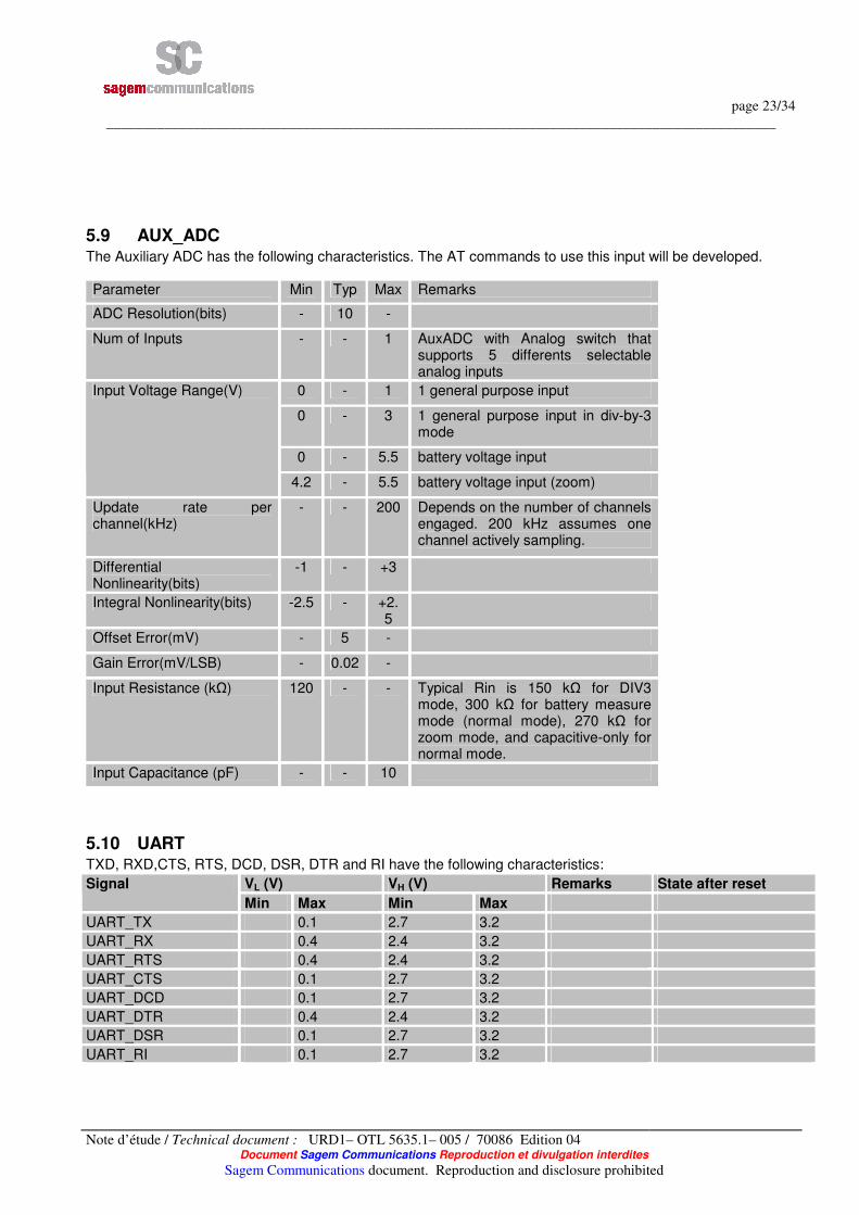
5.9 AUX_ADC The Auxiliary ADC has the following characteristics. The AT commands to use this input will be developed. Parameter Min Typ Max Remarks
ADC Resolution(bits) - 10 -
Num of Inputs - - 1 AuxADC with Analog switch that supports 5 differents selectable analog inputs
0 - 1 1 general purpose input
0 - 3 1 general purpose input in div-by-3 mode
0 - 5.5 battery voltage input
Input Voltage Range(V)
4.2 - 5.5 battery voltage input (zoom)
Update rate per channel(kHz)
- - 200 Depends on the number of channels engaged. 200 kHz assumes one channel actively sampling.
Differential Nonlinearity(bits)
-1 - +3
Integral Nonlinearity(bits) -2.5 - +2.5
Offset Error(mV) - 5 -
Gain Error(mV/LSB) - 0.02 -
Input Resistance (kΩ) 120 - - Typical Rin is 150 kΩ for DIV3 mode, 300 kΩ for battery measure mode (normal mode), 270 kΩ for zoom mode, and capacitive-only for normal mode.
Input Capacitance (pF) - - 10
5.10 UART TXD, RXD,CTS, RTS, DCD, DSR, DTR and RI have the following characteristics:
VL (V) VH (V) Remarks State after reset Signal
Min Max Min Max
UART_TX 0.1 2.7 3.2
UART_RX 0.4 2.4 3.2
UART_RTS 0.4 2.4 3.2
UART_CTS 0.1 2.7 3.2
UART_DCD 0.1 2.7 3.2
UART_DTR 0.4 2.4 3.2
UART_DSR 0.1 2.7 3.2
UART_RI 0.1 2.7 3.2
page 24/34
____________________________________________________________________________________________
Note d’étude / Technical document : URD1– OTL 5635.1– 005 / 70086 Edition 04
Document Sagem Communications Reproduction et divulgation interdites
Sagem Communications document. Reproduction and disclosure prohibited
5.11 AUDIO SIGNALS
5.11.1 Audio Inputs
The audio inputs contain the following characteristics: Parameter Min Typ Max Test Conditions
Maximum input range 1.4V With Gain = - 6dB
Nominal reference level 16mV Typical value Gain = + 34dB
Input Micro amplifier gain (dB) -6 + 50
5.11.2 Audio Outputs
The audio outputs contain the following characteristics: Parameter Min Typ Max Test Conditions
Maximum output range 2.8 Vpp
Load resistance (Ω) 32
Output amplifier gain (dB) -28 - 8

page 25/34
____________________________________________________________________________________________
Note d’étude / Technical document : URD1– OTL 5635.1– 005 / 70086 Edition 04
Document Sagem Communications Reproduction et divulgation interdites
Sagem Communications document. Reproduction and disclosure prohibited
6. ENVIRONMENTAL SPECIFICATION
Parameter
Min Max
Ambient temperature Normal range
-20°C +80°C
Ambient temperature Extended range
-40°C +85°C
Storage temperature -40°C +85°C
Long damp heat Operating conditions
Tested at +60°C, 95% RH during 504 hours
Short damp heat Storage and transportation conditions
Tested at +40°C, 95% RH during 96 hours
6.1 NORMAL RANGE, FROM -20°C TO +80°C:
Performance is qualified by SAGEM in the range of -20°C to +80°C.
6.2 EXTENDED RANGE, FROM -40°C TO -20°C AND FROM +80°C TO +85°C (TBC):
Inside this extended range, the operability is guaranteed by SAGEM. However, performance degradation as
power consumption or RF parameters could occur and will be defined later:
Power consumption:
(TBD)
Sensitivity in GSM850, GSM900, DCS1800, PCS1900:
(TBD) TX in GSM850, GSM900, DCS1800, PCS1900:
(TDD)
6.3 OUT OF OPERATIONAL RANGE: No operation is guaranteed by SAGEM out of the operational range. No operating tests are made below -40°c and above +85°c.

page 26/34
____________________________________________________________________________________________
Note d’étude / Technical document : URD1– OTL 5635.1– 005 / 70086 Edition 04
Document Sagem Communications Reproduction et divulgation interdites
Sagem Communications document. Reproduction and disclosure prohibited
7. ESD
Using human body model from JEDEC JESD 22-A114 standard, the HiLo can stand for +/-2kV ESD on all pins of the 40 points connector and on the RF connector.

page 27/34
____________________________________________________________________________________________
Note d’étude / Technical document : URD1– OTL 5635.1– 005 / 70086 Edition 04
Document Sagem Communications Reproduction et divulgation interdites
Sagem Communications document. Reproduction and disclosure prohibited
8. MECHANICAL SPECIFICATION
8.1 PHYSICAL DIMENSIONS
Whole size: 27 x 27 x 3.6
Figure 5: HiLo interface
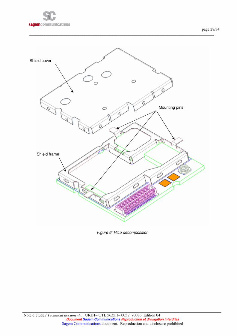
8.2 ASSEMBLY Shield frame is soldered on HiLo PCB; Shield cover is assembled with shield frame and removable. The recommended solution to fix the HiLo module is to manually solder the three mounting pins (represented on Figure 5 and Figure 6) on the motherboard. The solder pad geometries for the mounting pins are given in Figure 8
Antenna Hot Point
Mounting pins
Ground Pad
Pin 40
Pin 21
RF connector
Board to Board connector
Pin 20
Pin 1
page 28/34
____________________________________________________________________________________________
Note d’étude / Technical document : URD1– OTL 5635.1– 005 / 70086 Edition 04
Document Sagem Communications Reproduction et divulgation interdites
Sagem Communications document. Reproduction and disclosure prohibited
Figure 6: HiLo decomposition
Shield cover
Shield frame
Mounting pins

page 29/34
____________________________________________________________________________________________
Note d’étude / Technical document : URD1– OTL 5635.1– 005 / 70086 Edition 04
Document Sagem Communications Reproduction et divulgation interdites Sagem Communications document. Reproduction and disclosure prohibited
Figure 7: HiLo dimensions
page 30/34
____________________________________________________________________________________________
Note d’étude / Technical document : URD1– OTL 5635.1– 005 / 70086 Edition 04
Document Sagem Communications Reproduction et divulgation interdites Sagem Communications document. Reproduction and disclosure prohibited
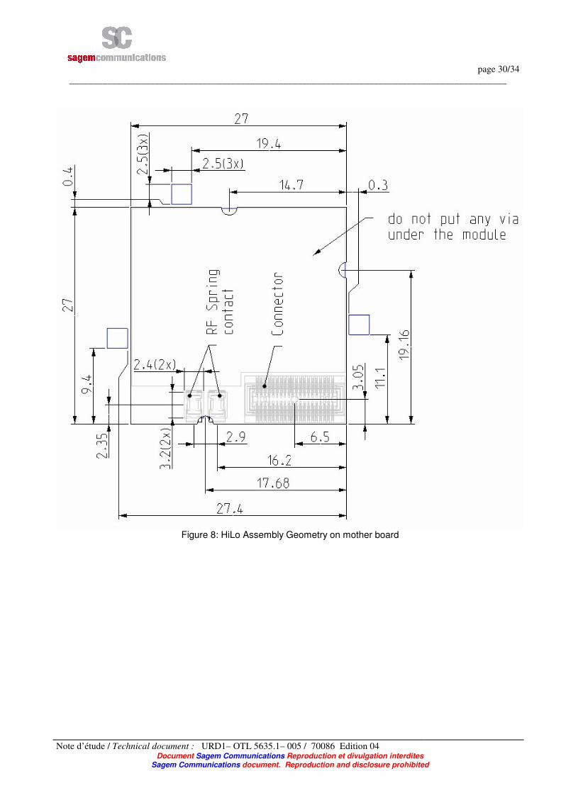
Figure 8: HiLo Assembly Geometry on mother board
page 31/34
____________________________________________________________________________________________
Note d’étude / Technical document : URD1– OTL 5635.1– 005 / 70086 Edition 04
Document Sagem Communications Reproduction et divulgation interdites Sagem Communications document. Reproduction and disclosure prohibited
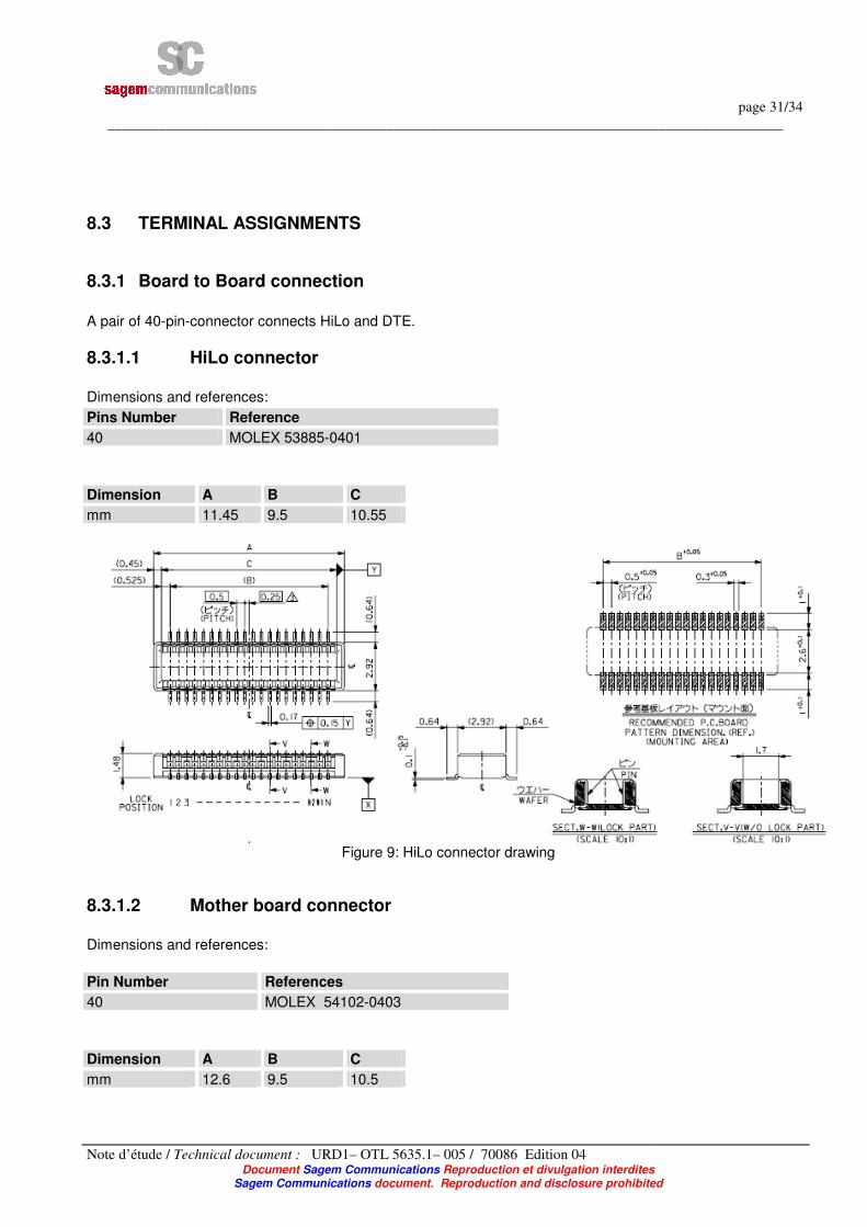
8.3 TERMINAL ASSIGNMENTS
8.3.1 Board to Board connection
A pair of 40-pin-connector connects HiLo and DTE.
8.3.1.1 HiLo connector
Dimensions and references:
Pins Number Reference
40 MOLEX 53885-0401
Dimension A B C
mm 11.45 9.5 10.55
Figure 9: HiLo connector drawing
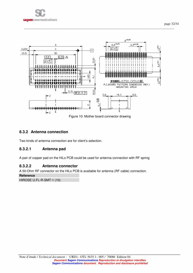
8.3.1.2 Mother board connector
Dimensions and references:
Pin Number References
40 MOLEX 54102-0403
Dimension A B C
mm 12.6 9.5 10.5
page 32/34
____________________________________________________________________________________________
Note d’étude / Technical document : URD1– OTL 5635.1– 005 / 70086 Edition 04
Document Sagem Communications Reproduction et divulgation interdites Sagem Communications document. Reproduction and disclosure prohibited
Figure 10: Mother board connector drawing
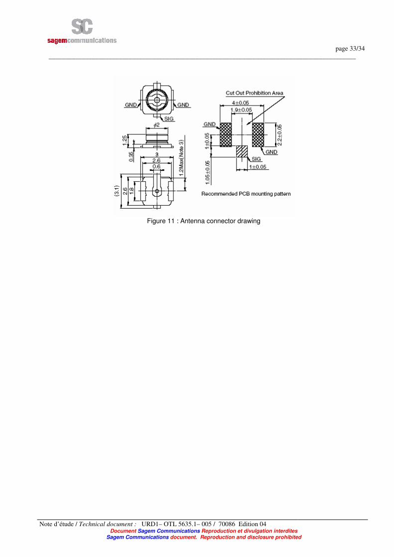
8.3.2 Antenna connection
Two kinds of antenna connection are for client’s selection.
8.3.2.1 Antenna pad
A pair of copper pad on the HiLo PCB could be used for antenna connection with RF spring
8.3.2.2 Antenna connector
A 50-Ohm RF connector on the HiLo PCB is available for antenna (RF cable) connection.
Reference
HIROSE U.FL-R-SMT-1 (10)
page 33/34
____________________________________________________________________________________________
Note d’étude / Technical document : URD1– OTL 5635.1– 005 / 70086 Edition 04
Document Sagem Communications Reproduction et divulgation interdites Sagem Communications document. Reproduction and disclosure prohibited
Figure 11 : Antenna connector drawing
page 34/34
____________________________________________________________________________________________
Note d’étude / Technical document : URD1– OTL 5635.1– 005 / 70086 Edition 04
Document Sagem Communications Reproduction et divulgation interdites Sagem Communications document. Reproduction and disclosure prohibited
9. REFERENCE DOCUMENTS
[1] URD1 5635.1 – 007 HiLo application note