si4020 universal ism crystal si4020 reference rfp · pdf fileremote automatic meter reading ....
TRANSCRIPT

1
Si4020-DS Rev 1.9r 0308 www.silabs.com/integration
Si4020 Universal ISM Band FSK Transmitter DESCRIPTION
Silicon Labs’ Si4020 is a single chip, low power, multi-channel FSK
transmitter designed for use in applications requiring FCC or ETSI
conformance for unlicensed use in the 315, 433, 868, and 915 MHz bands.
Used in conjunction with IA4320, Silicon Labs’ FSK receiver, the Si4020
transmitter feature EZRadioTM technology, which produces a flexible, low
cost, and highly integrated solution that does not require production
alignments. All required RF functions are integrated. Only an external crystal
and bypass filtering are needed for operation.
The Si4020 features a completely integrated PLL for easy RF design, and its
rapid settling time allows for fast frequency hopping, bypassing multipath
fading and interference to achieve robust wireless links. In addition, highly
stable and accurate FSK modulation is accomplished by direct closed-loop
modulation with bit rates up to 256 kbps. The PLL’s high resolution allows
the use of multiple channels in any of the bands.
The integrated power amplifier of the transmitter has an open-collector
differential output that directly drive a loop antenna with programmable
output level. No additional matching network is required. An automatic
antenna tuning circuit is built in to avoid costly trimming procedures and de-
tuning due to the “hand effect”.
For low-power applications, the device supports automatic activation from
sleep mode. Active mode can be initiated by several wake-up events (on-chip
timer timeout, low supply voltage detection, or activation of any of the four
push-button inputs).
The Si4020’s on-chip digital interface supports both a microcontroller mode
and an EEPROM mode. The latter allows complete data transmitter operation
without a microcontroller (both control commands and data are read from
the EEPROM). Any wake-up event can start a transmission of the
corresponding data stored in the EEPROM.
FUNCTIONAL BLOCK DIAGRAM
CRYSTAL
OSCILLATORSYNTHESIZER
LOW
BATTERY
DETECT
WAKE-UP
TIMER
CONTROLLER
REFERENCE
LOAD CAP
LOW BAT
TRESHOLD
TIMEOUT
PERIOD
CLOCK FREQUENCY
LEVEL
RFP
RFN
nIRQ/nLBD
CLK/SDO
SDI
SCK
nSEL
FSK
PB4PB3PB2PB1
VSS
VDD
MOD
XTL
OOK
Si4020
PIN ASSIGNMENT
SDI
SCK
nSEL
PB1
PB2
PB3
PB4
CLK
FSK
VDD
nIRQ
RFP
RFN
MOD
VSS
XTL
1
2
4
5
3
6
7
8
16
15
13
12
14
11
10
9
SDI
SCK
nSEL
PB1
PB2
PB3
PB4
SDO
FSK
VDD
nLBD
RFP
RFN
MOD
VSS
XTL
1
2
4
5
3
6
7
8
16
15
13
12
14
11
10
9
Microcontroller Mode EEPROM Mode
This document refers to Si4020-IC Rev I1.
See www.silabs.com/integration for any applicable
errata. See back page for ordering information.
FEATURES
Fully integrated (low BOM, easy design-in)
No alignment required in production
Fast settling, programmable, high-resolution PLL
Fast frequency hopping capability
Stable and accurate FSK modulation with programmable
deviation
High bit rate (up to 256 kbps)
Direct loop antenna drive
Automatic antenna tuning circuit
Programmable output power level
Alternative OOK support
EEPROM mode supported
SPI bus for applications with microcontroller
Clock output for microcontroller
Integrated programmable crystal load capacitor
Power-saving sleep mode
Multiple event handling options for wake-up activation
Push-button event handling with switch de-bounce
Wake-up timer
Low battery detection
2.2 to 5.4 V supply voltage
Low power consumption
Low standby current (0.3 µA)
Compact 16-pin TSSOP package
TYPICAL APPLICATIONS
Remote control
Home security and alarm
Wireless keyboard/mouse and other PC peripherals
Toy control
Remote keyless entry
Tire pressure monitoring
Telemetry
Personal/patient data logging
Remote automatic meter reading
Si4020
2
DETAILED DESCRIPTION
The Si4020 FSK transmitter is designed to cover the unlicensed
frequency bands at 315, 433, 868, and 915 MHz. The device
facilitates compliance with FCC and ETSI requirements.
PLL
The programmable PLL synthesizer determines the operating
frequency, while preserving accuracy based on the on-chip
crystal-controlled reference oscillator. The PLL’s high resolution
allows the usage of multiple channels in any of the bands. The
FSK deviation is selectable (from 30 to 240 kHz with 30 kHz
increments) to accommodate various bandwidth, data rate and
crystal tolerance requirements, and it is also highly accurate due
to the direct closed-loop modulation of the PLL. The transmitted
digital data can be sent asynchronously through the FSK pin or
over the control interface using the appropriate command.
The RF VCO in the PLL performs automatic calibration, which
requires only a few microseconds. To ensure proper operation in
the programmed frequency band, the RF VCO is automatically
calibrated upon activation of the synthesizer. If temperature or
supply voltage change significantly or operational band has
changed, VCO recalibration is recommended.. Recalibration can
be initiated at any time by switching the synthesizer off and back
on again.
RF Power Amplifier (PA)
The power amplifier has an open-collector differential output and
can directly drive a loop antenna with a programmable output
power level. An automatic antenna tuning circuit is built in to
avoid costly trimming procedures and the so-called “hand effect.”
The transmitters can operate in On-Off Keying (OOK) mode by
switching the power amplifier on and off. When the appropriate
control bit is set using the Power Setting Command, the FSK pin
becomes an enable input (active high) for the power amplifier.
Crystal Oscillator
The chip has a single-pin crystal oscillator circuit, which provides
a 10 MHz reference signal for the PLL. To reduce external parts
and simplify design, the crystal load capacitor is internal and
programmable. Guidelines for selecting the appropriate crystal
can be found later in this datasheet.
The transmitters can supply the clock signal for the
microcontroller, so accurate timing is possible without the need
for a second crystal. When the chip receives a Sleep Command
from the microcontroller and turns itself off, it provides several
further clock pulses (“clock tail”) for the microcontroller to be
able to go to idle or sleep mode. The length of the clock tail is
programmable.
Low Battery Voltage Detector
The low battery voltage detector circuit monitors the supply
voltage and generates an interrupt if it falls below a
programmable threshold level. The detector circuit has 50 mV
hysteresis.
Wake-Up Timer
The wake-up timer has very low current consumption (1.5 uA
typical) and can be programmed from 1 ms to several days with
an accuracy of ±5%.
It calibrates itself to the crystal oscillator at every startup. When
the oscillator is switched off, the calibration circuit switches on
the crystal oscillator only long enough for a quick calibration (a
few milliseconds) to facilitate accurate wake-up timing.
Event Handling
In order to minimize current consumption, the device supports
sleep mode. Active mode can be initiated by several wake-up
events: timeout of wake-up timer, detection of low supply
voltage, pressing any of the four push-button inputs, or through
the serial interface. The push-button inputs can be driven by a
logic signal from a microcontroller or controlled directly by
normally open switches. Pull-up resistors are integrated.
If any wake-up event occurs, the wake-up logic generates an
interrupt, which can be used to wake up the microcontroller,
effectively reducing the period the microcontroller has to be
active. The cause of the interrupt can be read out from the
transmitters by the microcontroller through the nIRQ pin.
Interface
An SPI compatible serial interface lets the user select the
operating frequency band and center frequency of the
synthesizer, polarity and deviation of FSK modulation, and output
power level. Division ratio for the microcontroller clock, wake-up
timer period, and low battery detector threshold are also
programmable. Any of these auxiliary functions can be disabled
when not needed. All parameters are set to default after power-
on; the programmed values are retained during sleep mode.
EEPROM Mode
In simple applications, the on-chip digital controller provides the
transmitters with direct interface to a serial (SPI) EEPROM. In this
case, no external microcontroller is necessary. Wake-up events
initiate automatic readout of the assigned command sequence
from EEPROM memory. For every event, there is a dedicated
starting address available in the EEPROM.
Programming the EEPROM is very simple. Any control command
can be programmed in the EEPROM sequentially (same as in
microcontroller mode).
The internal power-on reset (POR) is a dedicated event, which
can be used to program the basic settings of the transmitters. In
this case the chip starts to read out the preprogrammed data
from the 00h address in EEPROM. Data can be transmitted with
the help of the Data Transmit Command, which tells the
transmitters how many bytes must be transmitted. The whole
process finishes with a Sleep Command.

Si4020
3
PACKAGE PIN DEFINITIONS, MICROCONTROLLER MODE
Pin type key: D=digital, A=analog, S=supply, I=input, O=output, IO=input/output
Microcontroller Mode Pin Assignment
SDI
SCK
nSEL
PB1
PB2
PB3
PB4
CLK
FSK
VDD
nIRQ
RFP
RFN
MOD
VSS
XTL
1
2
4
5
3
6
7
8
16
15
13
12
14
11
10
9
Pin Name Type Function
1 SDI DI Data input of serial control interface
2 SCK DI Clock input of serial control interface
3 nSEL DI Chip select input of serial control interface (active low)
4 PB1 DI Push-button input #1 (active low with internal pull-up resistor)
5 PB2 DI Push-button input #2 (active low with internal pull-up resistor)
6 PB3 DI Push-button input #3 (active low with internal pull-up resistor)
7 PB4 DI Push-button input #4 (active low with internal pull-up resistor)
8 CLK DO Microcontroller clock (1 MHz-10 MHz)
9 XTL AIO Crystal connection (other terminal of crystal to VSS)
10 VSS S Ground reference
11 MOD DI Connect to logic high (microcontroller mode)
12 RFN AO Power amplifier output (open collector)
13 RFP AO Power amplifier output (open collector)
14 nIRQ DO Interrupt request output for microcontroller (active low) and status read output
15 VDD S Positive supply voltage
16 FSK DI Serial data input for FSK modulation
Si4020
4
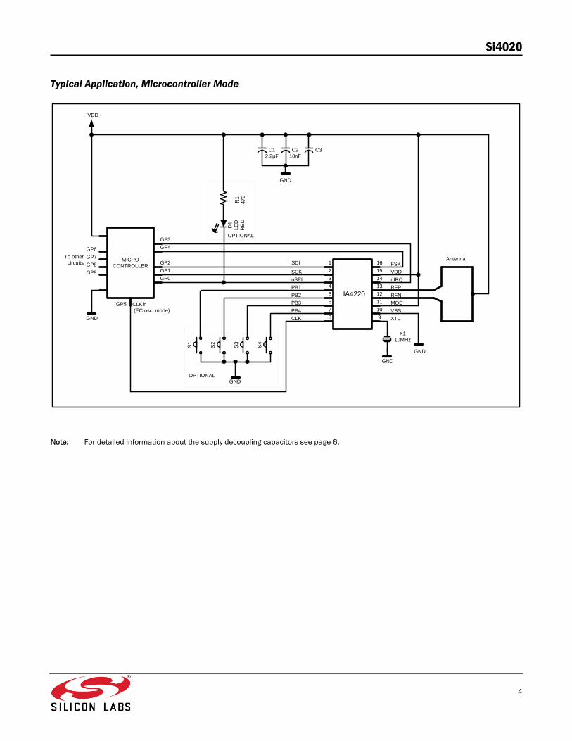
Typical Application, Microcontroller Mode
VDD
XTL
VSS
MOD
RFN
RFP
nIRQ
VDD
FSK
X1
10MHz
GND
GND
GND
1 16
2 15
3 14
4 13
5 12
6 11
7 10
8 9
IA4220
GND
C3C2
10nF
C1
2.2µF
R1
47
0
D1
LE
D
RE
DGP4
GP3
GP2
GP1
MICRO
CONTROLLER
GP0
CLKin
(EC osc. mode)
SDI
SCK
nSEL
PB1
PB2
PB3
PB4
CLK
GP5
OPTIONAL
S1
S2
S3
S4
OPTIONAL
GND
GP6
GP7
GP8
GP9
To other
circuitsAntenna
Note: For detailed information about the supply decoupling capacitors see page 6.

Si4020
5
PACKAGE PIN DEFINITIONS, EEPROM MODE
Pin type key: D=digital, A=analog, S=supply, I=input, O=output, IO=input/output
EEPROM Mode Pin Assignment
SDI
SCK
nSEL
PB1
PB2
PB3
PB4
SDO
FSK
VDD
nLBD
RFP
RFN
MOD
VSS
XTL
1
2
4
5
3
6
7
8
16
15
13
12
14
11
10
9
Pin Name Type Function
1 SDI DI Data input of serial control interface
2 SCK DO Clock output of serial control interface
3 nSEL DO Chip select output of serial control interface (active low)
4 PB1 DI Push-button input #1 (active low with internal pull-up resistor)
5 PB2 DI Push-button input #2 (active low with internal pull-up resistor)
6 PB3 DI Push-button input #3 (active low with internal pull-up resistor)
7 PB4 DI Push-button input #4 (active low with internal pull-up resistor)
8 SDO DO Data output of serial control interface
9 XTL AIO Crystal connection (other terminal of crystal to VSS)
10 VSS S Ground reference
11 MOD DI Connect to logic low (EEPROM mode)
12 RFN AO Power amplifier output (open collector)
13 RFP AO Power amplifier output (open collector)
14 nLBD DO Low battery voltage detector output (active low)
15 VDD S Positive supply voltage
16 FSK DI Not used, connect to VDD or VSS

Si4020
6
Typical Application, EEPROM Mode
VDD
1 8
3
72
6
4 5
EEPROM
25AA080
1 16
2 15
3 14
4 13
5 12
6 11
7 10
8 9
IA4220
SD
ISCK
nSEL
PB1
PB2
PB3
PB4
SD0 XTL
VSS
MOD
RFN
RFP
nLBD
VDD
FSK
nCS
SO
nWP
GND SI
SCK
HOLD
VCC
R1
47
0
D1
LE
D
RE
D
X1
10MHz
GND
GND GND
GND
GND
S1
S2
S3
S4
C3C2
10nF
C1
2.2µF
x
Antenna
OPTIONAL
Recommended supply decoupling capacitor values
C2 and C3 should be 0603 size ceramic capacitors to achieve the best supply decoupling. The capacitor values are valid for both
stand-alone and microcontroller mode.
Band [MHz] C1 C2 C3
315 2.2µF 10nF 390pF
433 2.2µF 10nF 220pF
868 2.2µF 10nF 47pF
915 2.2µF 10nF 33pF

Si4020
7
GENERAL DEVICE SPECIFICATIONS
All voltages are referenced to Vss, the potential on the ground reference pin VSS.
Absolute Maximum Ratings (non-operating)
Symbol Parameter Min Max Units
Vdd Positive supply voltage -0.5 6.0 V
Vin Voltage on any pin except open collector outputs -0.5 Vdd+0.5 V
Voc Voltage on open collector outputs -0.5 6.0 V
Iin Input current into any pin except VDD and VSS -25 25 mA
ESD Electrostatic discharge with human body model 1000 V
Tst Storage temperature -55 125 ºC
Tld Lead temperature (soldering, max 10 s) 260 ºC
Recommended Operating Range
Symbol Parameter Min Max Units
Vdd Positive supply voltage 2.2 5.4 V
Voc Voltage on open collector outputs (Max 6.0 V) Vdd - 1 Vdd + 1 V
Top Ambient operating temperature -40 85 ºC
ELECTRICAL SPECIFICATION
(Min/max values are valid over the whole recommended operating range, typical conditions: Top = 27 oC; Vdd = Voc = 2.7 V)
DC Characteristics
Symbol Parameter Conditions/Notes Min Typ Max Units
Idd_TX_0 Supply current (TX mode, Pout = 0 dBm)
315 MHz band 9
mA 433 MHz band 10
868 MHz band 12
915 MHz band 13
Idd_TX_PMAX Supply current (TX mode, Pout = Pmax)
315 MHz band 11
mA 433 MHz band 12
868 MHz band 14
915 MHz band 15
Ipd Standby current in sleep mode All blocks disabled (Note 1) 0.3 µA
Iwt Wake-up timer current consumption 1.5 µA
Ilb Low battery detector current consumption
0.5 µA
Ix Idle current Only crystal oscillator is on 1.5 mA
Vlba Low battery detection accuracy 75 mV
Vlb Low battery detector threshold Programmable in 0.1 V steps 2.2 5.3 V
Vil Digital input low level 0.3*Vdd V
Vih Digital input high level 0.7*Vdd V
Iil Digital input current Vil = 0 V -1 1 µA
Iih Digital input current Vih = Vdd, Vdd = 5.4 V -1 1 µA
Vol Digital output low level Iol = 2 mA 0.4 V
Voh Digital output high level Ioh = -2 mA Vdd-0.4 V
Note for table above is on page 7.

Si4020
8
AC Characteristics
Symbol Parameter Conditions/Notes Min Typ Max Units
fref PLL reference frequency Crystal operation mode is parallel (Note 2) 8 10 12 MHz
fo Output frequency (programmable)
315 MHz band, 2.5 kHz resolution 310.24 319.75
MHz 433 MHz band, 2.5 kHz resolution 430.24 439.75
868 MHz band, 5.0 kHz resolution 860.48 879.51
915 MHz band, 7.5 kHz resolution 900.72 929.27
tlock PLL lock time Frequency error < 10 kHz after 10 MHz step
20 µs
tsp PLL startup time After turning on from idle mode, with crystal oscillator already stable
250 µs
IOUT Open collector output current (Note 3) At all bands 0.1 2.5 mA
PmaxL Available output power (315 and 433 MHz band)
With optimal antenna impedance (Note 4)
3 dBm
PmaxH Available output power (868 and 915 MHz band)
With optimal antenna impedance (Note 4)
1 dBm
Pout Typical output power Selectable in 3 dB steps (Note3) Pmax-21 Pmax dBm
Psp Spurious emission At max power with loop antenna (Note 5)
-50 dBc
Co Output capacitance (set by the automatic antenna tuning circuit)
At low bands 1.5 2.3 3.1 pF
At high bands 1.6 2.2 2.8
Qo Quality factor of the output capacitance
16 18 22
Lout Output phase noise 100 kHz from carrier -75
dBc/Hz 1 MHz from carrier -85
BRFSK FSK bit rate 256 kbps
BROOK OOK bit rate 512 kbps
dffsk FSK frequency deviation Programmable in 30 kHz steps 30 240 kHz
Cxl Crystal load capacitance See Crystal Selection Guidelines
Programmable in 0.5 pF steps, tolerance +/- 10%
8.5 16 pF
tPOR Internal POR timeout (Note 6)
After Vdd has reached 90% of final value 100 ms
tsx Crystal oscillator startup time Crystal ESR < 100 Ohms (Note 7) 1 5 ms
tPBt Wake-up timer clock accuracy Crystal oscillator must be enabled to ensure proper calibration at startup (Note 7)
+/-10% ms
twake-up Programmable wake-up time 1 2 · 109 ms
Cin, D Digital input capacitance 2 pF
tr, f Digital output rise/fall time 15 pF pure capacitive load 10 ns
All notes for table above are on page 7.

Si4020
9
Note 1: Using a CR2032 battery (225 mAh capacity), the expected battery life is greater than 2 years using a 60-second wake-up period
for sending 100 byte packets in length at 19.2 kbps with +3 dBm output power in the 915 MHz band.
Note 2: Using anything but a 10 MHz crystal is allowed but not recommended because all crystal-referred timing and frequency
parameters will change accordingly.
Note 3: Adjustable in 8 steps.
Note 4: Optimal antenna admittance/impedance for the Si4020:
Yantenna [S] Zantenna [Ohm] Lantenna [nH]
315 MHz 9.4E-4 - j4.5E-3 43 + j214 112.00
434 MHz 8.4E-4 - j6.25E-3 21 + j157 59.00
868 MHz 1.15E-3 - j1.2E-2 7.9 + j83 15.30
915 MHz 1.2E-3 - j1.25E-2 7.6 + j79 13.90
Note 5: With selective resonant antennas (see: Application Notes available from http://www.silabs.com/integration).
Note 6: During this period, no commands are accepted by the chip. For detailed information see the Reset modes section.
Note 7: The crystal oscillator start-up time strongly depends on the capacitance seen by the oscillator. Using low capacitance and low ESR
crystal is recommended. When designing the PCB layout keep the trace connecting to the crystal short to minimize stray
capacitance.

Si4020
10
TYPICAL PERFORMANCE DATA
Unmodulated RF Spectrum
The output spectrum is measured at different frequencies. The output is loaded with 50 Ohms through a matching network.
15:18:59 Oct 29, 2003
Ref -10 dBm #Atten 5 dB
Mkr1 434.0630 MHz
-23.41 dBm
Samp
Log
10
dB/
VAvg
100
W1 S2
S3 FC
AA
Center 434.1 MHz
zHk01WBVzHk01WBseR
Span 2 MHz
Sweep 40.74 ms (2001 pts)
1
15:20:49 Oct 29, 2003
Ref -10 dBm #Atten 5 dB
Mkr1 868.0680 MHz
-23.23 dBm
Samp
Log
10
dB/
VAvg
100
W1 S2
S3 FC
AA
Center 868.1 MHz
zHk01WBVzHk01WBseR
Span 2 MHz
Sweep 40.74 ms (2001 pts)
1
15:37:47 Dec 15, 2003
Ref -10 dBm Atten 5 dB
Mkr1 315.0010 MHz
-22.7 dBm
Samp
Log
10
dB/
VAvg
100
W1 S2
S3 FC
AA
Center 315 MHz
zHk01WBVzHk01WBseR
Span 2 MHz
Sweep 40.74 ms (2001 pts)
1
15:28:02 Dec 15, 2003
Ref -10 dBm Atten 5 dB
Mkr1 915.0000 MHz
-24.63 dBm
Samp
Log
10
dB/
VAvg
100
W1 S2
S3 FC
AA
Center 915 MHz
zHk01WBVzHk01WBseR
Span 2 MHz
Sweep 40.74 ms (2001 pts)
1
At 315 MHz At 433 MHz
At 868 MHz At 915 MHz

Si4020
11
Modulated RF Spectrum
At 433 MHz with
180 kHz Deviation at 64 kbps
At 868 MHz with
180 kHz Deviation at 64 kbps At 433MHz with180 kHz deviation at 64 kbps
15:46:09 Oct 29, 2003
Ref -10 dBm Atten 5 dB#PeakLog10dB/
VAvg100W1S2S3 FC
AA
Center 434 MHzRes BW 10 kHz VBW 100 kHz
Span 2 MHzSweep 20.07 ms (2001 pts)
At 868MHz with180 kHz deviation at 64 kbps
15:43:45 Oct 29, 2003
Ref -10 dBm Atten 5 dB#PeakLog10dB/
VAvg100W1S2S3 FC
AA
Center 868 MHzRes BW 10 kHz VBW 100 kHz
Span 2 MHzSweep 20.07 ms (2001 pts)
Spurious RF Spectrum
With 10 MHz CLK Output Enabled at 433 MHz
Antenna Tuning Characteristics
750–970 MHz Spurious RF spectrumWith 10 MHz CLK output enabled at 433MHz
16:29:03 Jun 17, 2003
Ref 0 dBm Atten 10 dBMkr1 ∆ 20.0 MHz
-55.11 dB#PeakLog10dB/
W1S2S3 FC
AA
Center 434.8 MHz#Res BW 3 kHz #VBW 300 Hz
Span 50 MHzSweep 45.47 s (401 pts)
1
1R
Marker ∆20.000000 MHz-55.11 dB
Antenna tuning characteristics750-970 MHz
16:54:54 Mar 11, 2003
Ref -36 dBm #Atten 0 dBMkr1 915.0 MHz
-37.62 dBmPeakLog1dB/
V1 M2S3 FC
AA
Start 700 MHz#Res BW 1 MHz VBW 1 MHz
Stop 1.05 GHzSweep 50 ms (401 pts)
1
*
Marker915.000000 MHz-37.62 dBm
The antenna tuning characteristics was recorded in “max-hold” state of the spectrum analyzer. During the measurement, the
transmitters were forced to change frequencies by forcing an external reference signal to the XTL pin. While the carrier was changing
the antenna tuning circuit switched trough all the available states of the tuning circuit. The graph clearly demonstrates that while the
complete output circuit had about a 40 MHz bandwidth, the tuning allows operating in a 220 MHz band. In other words the tuning
circuit can compensate for 25% variation in the resonant frequency due to any process or manufacturing spread.

Si4020
12
CONTROL INTERFACE
Commands to the transmitters are sent serially. Data bits on pin SDI are shifted into the device upon the rising edge of the clock on
pin SCK whenever the chip select pin nSEL is low. When the nSEL signal is high, it initializes the serial interface. The number of bits
sent is an integer multiple of 8. All commands consist of a command code, followed by a varying number of parameter or data bits.
All data are sent MSB first (e.g. bit 15 for a 16-bit command). Bits having no influence (don’t care) are indicated with X. The Power
On Reset (POR) circuit sets default values in all control and command registers.
Timing Specification
Timing Diagram
Symbol Parameter Minimum value [ns]
tCH Clock high time 25
tCL Clock low time 25
tSS Select setup time (nSEL falling edge to SCK rising edge) 10
tSH Select hold time (SCK falling edge to nSEL rising edge) 10
tSHI Select high time 25
tDS Data setup time (SDI transition to SCK rising edge) 5
tDH Data hold time (SCK rising edge to SDI transition) 5
tOD Data delay time 10
tBL Push-button input low time 25
Si4020
13
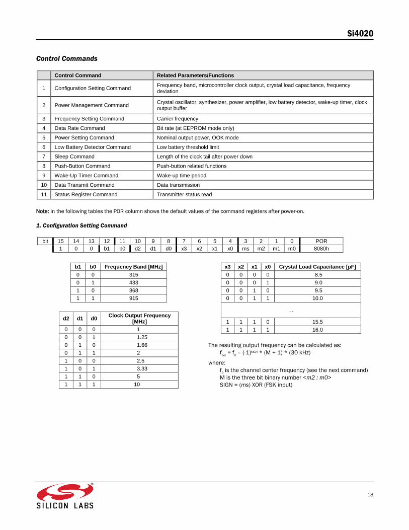
Control Commands
Control Command Related Parameters/Functions
1 Configuration Setting Command Frequency band, microcontroller clock output, crystal load capacitance, frequency deviation
2 Power Management Command Crystal oscillator, synthesizer, power amplifier, low battery detector, wake-up timer, clock output buffer
3 Frequency Setting Command Carrier frequency
4 Data Rate Command Bit rate (at EEPROM mode only)
5 Power Setting Command Nominal output power, OOK mode
6 Low Battery Detector Command Low battery threshold limit
7 Sleep Command Length of the clock tail after power down
8 Push-Button Command Push-button related functions
9 Wake-Up Timer Command Wake-up time period
10 Data Transmit Command Data transmission
11 Status Register Command Transmitter status read
Note: In the following tables the POR column shows the default values of the command registers after power-on.
1. Configuration Setting Command
bit 15 14 13 12 11 10 9 8 7 6 5 4 3 2 1 0 POR
1 0 0 b1 b0 d2 d1 d0 x3 x2 x1 x0 ms m2 m1 m0 8080h
b1 b0 Frequency Band [MHz]
0 0 315
0 1 433
1 0 868
1 1 915
d2 d1 d0 Clock Output Frequency
[MHz]
0 0 0 1
0 0 1 1.25
0 1 0 1.66
0 1 1 2
1 0 0 2.5
1 0 1 3.33
1 1 0 5
1 1 1 10
x3 x2 x1 x0 Crystal Load Capacitance [pF]
0 0 0 0 8.5
0 0 0 1 9.0
0 0 1 0 9.5
0 0 1 1 10.0
…
1 1 1 0 15.5
1 1 1 1 16.0
The resulting output frequency can be calculated as:
fout
= f0 – (-1)SIGN * (M + 1) * (30 kHz)
where:
f0 is the channel center frequency (see the next command)
M is the three bit binary number <m2 : m0>
SIGN = (ms) XOR (FSK input)
Si4020
14
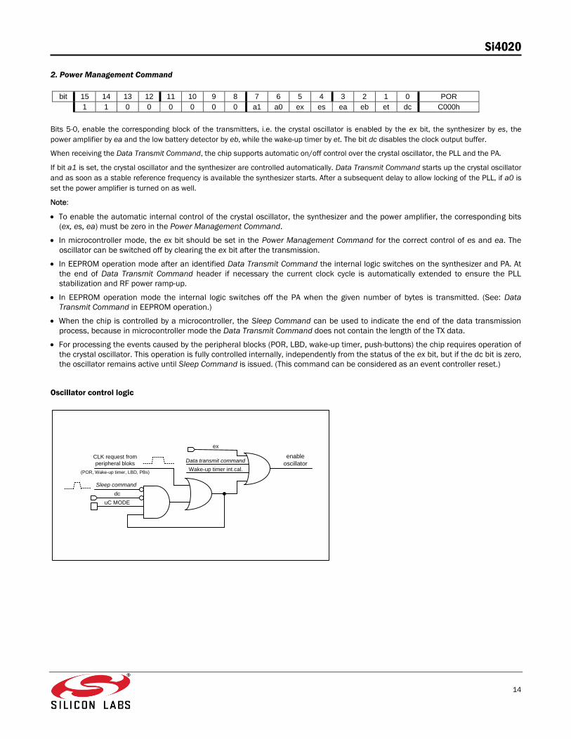
2. Power Management Command
bit 15 14 13 12 11 10 9 8 7 6 5 4 3 2 1 0 POR
1 1 0 0 0 0 0 0 a1 a0 ex es ea eb et dc C000h
Bits 5-0, enable the corresponding block of the transmitters, i.e. the crystal oscillator is enabled by the ex bit, the synthesizer by es, the
power amplifier by ea and the low battery detector by eb, while the wake-up timer by et. The bit dc disables the clock output buffer.
When receiving the Data Transmit Command, the chip supports automatic on/off control over the crystal oscillator, the PLL and the PA.
If bit a1 is set, the crystal oscillator and the synthesizer are controlled automatically. Data Transmit Command starts up the crystal oscillator
and as soon as a stable reference frequency is available the synthesizer starts. After a subsequent delay to allow locking of the PLL, if a0 is
set the power amplifier is turned on as well.
Note:
To enable the automatic internal control of the crystal oscillator, the synthesizer and the power amplifier, the corresponding bits
(ex, es, ea) must be zero in the Power Management Command.
In microcontroller mode, the ex bit should be set in the Power Management Command for the correct control of es and ea. The
oscillator can be switched off by clearing the ex bit after the transmission.
In EEPROM operation mode after an identified Data Transmit Command the internal logic switches on the synthesizer and PA. At
the end of Data Transmit Command header if necessary the current clock cycle is automatically extended to ensure the PLL
stabilization and RF power ramp-up.
In EEPROM operation mode the internal logic switches off the PA when the given number of bytes is transmitted. (See: Data
Transmit Command in EEPROM operation.)
When the chip is controlled by a microcontroller, the Sleep Command can be used to indicate the end of the data transmission
process, because in microcontroller mode the Data Transmit Command does not contain the length of the TX data.
For processing the events caused by the peripheral blocks (POR, LBD, wake-up timer, push-buttons) the chip requires operation of
the crystal oscillator. This operation is fully controlled internally, independently from the status of the ex bit, but if the dc bit is zero,
the oscillator remains active until Sleep Command is issued. (This command can be considered as an event controller reset.)
Oscillator control logic
ex
Wake-up timer int.cal.
dc
uC MODE
CLK request from
peripheral bloks
enable
oscillator
(POR, Wake-up timer, LBD, PBs)
Sleep command
Data transmit command

Si4020
15
3. Frequency Setting Command
bit 15 14 13 12 11 10 9 8 7 6 5 4 3 2 1 0 POR
1 0 1 0 f11 f10 f9 f8 f7 f6 f5 f4 f3 f2 f1 f0 A7D0h
The 12-bit parameter of the Frequency Setting Command
<f11 : f0> has the value F. The value F should be in the range
of 96 and 3903. When F is out of range, the previous value is
kept. The synthesizer center frequency f0 can be calculated as:
f0 = 10 MHz * C1 * (C2 + F/4000)
The constants C1 and C2 are determined by
the selected band as:
Band [MHz] C1 C2
315 1 31
433 1 43
868 2 43
915 3 30
Note:
For correct operation of the frequency synthesizer, the frequency and band of operation need to be programmed before the
synthesizer is started. Directly after activation of the synthesizer, the RF VCO is calibrated to ensure proper operation in the
programmed frequency band.
When coding for the Si4020, it is suggested that recalibration routines be added to compensate for significant changes in
temperature and supply voltages.
4. Data Rate Command
bit 15 14 13 12 11 10 9 8 7 6 5 4 3 2 1 0 POR
1 1 0 0 1 0 0 0 r7 r6 r5 r4 r3 r2 r1 r0 C800h
In EEPROM mode the transmitted bit rate is determined by the 8-bit value R (bits <r7 : r0>) as:
BR = 10 MHz / 29 / (R+1)
Apart from setting custom values, the standard bit rates from 2.4 to 115.2 kbps can be approximated with minimal error.
The commands are read out with a different fixed bit rate:
Fsck = 10 MHz / 29 / 3 [~115.2 kHz]
5. Power Setting Command
bit 7 6 5 4 3 2 1 0 POR
1 0 1 1 ook p2 p1 p0 B0h
The bit ook enables the OOK mode for the PA, in this case the data to be transmitted are received through the FSK pin.
p2 p1 p0 Relative Output Power [dB]
0 0 0 0
0 0 1 -3
0 1 0 -6
0 1 1 -9
1 0 0 -12
1 0 1 -15
1 1 0 -18
1 1 1 -21
The output power is given in the table as relative to the
maximum available power, which depends on the actual
antenna impedance. (See: Antenna Application Note
available from www.silabs.com/integration).

Si4020
16
6. Low Battery Detector Command
bit 15 14 13 12 11 10 9 8 7 6 5 4 3 2 1 0 POR
1 1 0 0 0 0 1 0 0 0 0 t4 t3 t2 t1 t0 C200h
The 5-bit value T of <t4 : t0> determines the threshold voltage Vlb of the detector:
Vlb = 2.25 V + T * 0.1 V
7. Sleep Command
bit 15 14 13 12 11 10 9 8 7 6 5 4 3 2 1 0 POR
1 1 0 0 0 1 0 0 s7 s6 s5 s4 s3 s2 s1 s0 C400h
The effect of this command depends on the Power Management Command. It immediately disables the power amplifier (if a0=1 and
ea=0) and the synthesizer (if a1=1 and es=0). Stops the crystal oscillator after S periods of the microcontroller clock (if a1=1 and
ex=0) to enable the microcontroller to execute all necessary commands before entering sleep mode itself. The 8-bit value S is
determined by bits <s7 : s0>.
8. Push-Button Command
bit 15 14 13 12 11 10 9 8 7 6 5 4 3 2 1 0 POR
1 1 0 0 1 0 1 0 p4 d1 d0 b4 b3 b2 b1 bc CA00h
If the corresponding bit was set (b1-b4) the event remains active while the button is pressed. In EEPROM mode, the chip is continuously
performing the routine assigned to the push-button while it is pressed. In microcontroller mode, the chip continuously generates interrupts
on nIRQ until the push-button is released. Weak pull-up currents are switched off when bc is high.
The d0, d1 bits set the de-bouncing time period:
d1 d0 De-bouncing Time [ms]
0 0 160
0 1 40
1 0 10
1 1 0 (Bypassed)
Note:
Until the de-bouncing time has expired, the crystal oscillator remains switched on, independent of the status of the ex bit in the
Power Management Command. (Because the circuit uses the crystal oscillator signal for timing.)
If the p4 bit is set, the controller performs the routine assigned to the fourth button when PB1 and PB2 are pressed down
simultaneously. With the addition of this feature, there is a way to build a device that uses 3 buttons, but performs 4 functions.
It is possible to detect multiple pressed push-buttons in both modes. In EEPROM mode the controller executes sequentially all the
routines belonging to the pressed buttons.

Si4020
17
Simultaneously Pressed Push-Button Detect by Microcontroller
Vdd
Microcontroller mode
SPI
nIRQ
POR
(internal)
Push button
input 2
Push button
input 1
POR PB1 PB1 PB2 PB1 PB2 PB1
Status rd Status rdStatus rd Status rd Status rd Status rd Status rd
PB_nIRQdly*
Note:
*PB_nIRQdly is equal with the
debounce time
Simplified Block Diagram of Push-Button 1–4 Inputs
To Digital glitch filter for
Push-button4
Push-button1,2,3
D Q
CLR
EVENT FLAG
SLEEP Command *
STAT. REG. READ Command **
COUNT/SINGLE
VDD
Note:
* In EEprom mode
** In uC controlled mode
Push-button1
Push-button2
Push-button4
Internal
blocker signal
to
Push-button1
and
Push-button2
p4
WEAK PULL-UP
ENABLE/DISABLE
VDD
With internal weak pull-up
POR, LBD, WAKE UP TIMER,
P. BUTTONS EVENT FLAGS
Notice:
Only one EVENT is
serviced simultaneously
the others are pending.
Digital glitch
filterCLK
CLR for P.B1,2
b1, b2, b3
bc
Si4020
18
9. Wake-Up Timer Command
bit 15 14 13 12 11 10 9 8 7 6 5 4 3 2 1 0 POR
1 1 1 r4 r3 r2 r1 r0 m7 m6 m5 m4 m3 m2 m1 m0 E000h
The wake-up time period can be calculated as:
Twake-up = M * 2R [ms] ,
where M is defined by the <m7 : m0> digital value and R is defined by the <r4 : r0> digital value.
The value of R should be in the range of 0 and 23. The maximum achievable wake-up time period can be up to 24 days.
Note:
For continual operation the et bit should be cleared and set at the end of every cycle.
Software reset: Sending FF00h command to the chip triggers software reset. For more details see the Reset modes section.
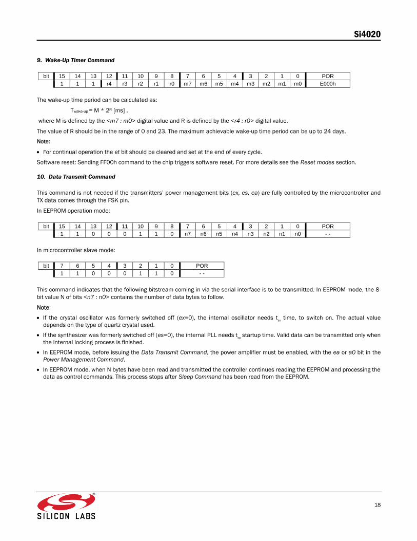
10. Data Transmit Command
This command is not needed if the transmitters’ power management bits (ex, es, ea) are fully controlled by the microcontroller and
TX data comes through the FSK pin.
In EEPROM operation mode:
bit 15 14 13 12 11 10 9 8 7 6 5 4 3 2 1 0 POR
1 1 0 0 0 1 1 0 n7 n6 n5 n4 n3 n2 n1 n0 - -
In microcontroller slave mode:
bit 7 6 5 4 3 2 1 0 POR
1 1 0 0 0 1 1 0 - -
This command indicates that the following bitstream coming in via the serial interface is to be transmitted. In EEPROM mode, the 8-
bit value N of bits <n7 : n0> contains the number of data bytes to follow.
Note:
If the crystal oscillator was formerly switched off (ex=0), the internal oscillator needs tsx time, to switch on. The actual value
depends on the type of quartz crystal used.
If the synthesizer was formerly switched off (es=0), the internal PLL needs tsp startup time. Valid data can be transmitted only when
the internal locking process is finished.
In EEPROM mode, before issuing the Data Transmit Command, the power amplifier must be enabled, with the ea or a0 bit in the
Power Management Command.
In EEPROM mode, when N bytes have been read and transmitted the controller continues reading the EEPROM and processing the
data as control commands. This process stops after Sleep Command has been read from the EEPROM.
Si4020
19
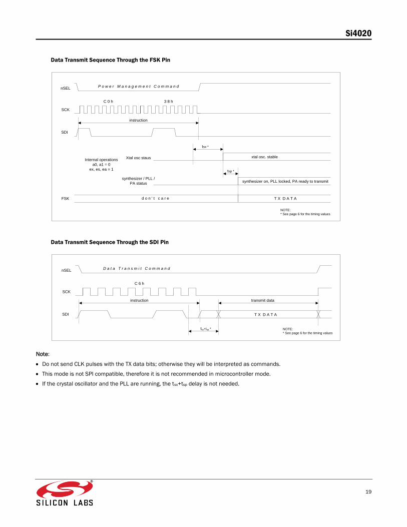
Data Transmit Sequence Through the FSK Pin
nSEL
SCK
SDI
instruction
Internal operations
a0, a1 = 0
ex, es, ea = 1
xtal osc. stableXtal osc staus
FSK T X D A T A
synthesizer on, PLL locked, PA ready to transmitsynthesizer / PLL /
PA status
tsx *
tsp *
C 0 h 3 8 h
d o n ' t c a r e
P o w e r M a n a g e m e n t C o m m a n d
NOTE:
* See page 6 for the timing values
Data Transmit Sequence Through the SDI Pin
nSEL
SCK
SDI
instruction
T X D A T A
transmit data
tsx+tsp *
D a t a T r a n s m i t C o m m a n d
NOTE:
* See page 6 for the timing values
C 6 h
Note:
Do not send CLK pulses with the TX data bits; otherwise they will be interpreted as commands.
This mode is not SPI compatible, therefore it is not recommended in microcontroller mode.
If the crystal oscillator and the PLL are running, the tsx+tsp delay is not needed.

Si4020
20
11. Status Register Read Command
bit 15 14 13 12 11 10 9 8 7 6 5 4 3 2 1 0 POR
1 1 0 0 1 1 0 0 0 0 0 0 0 0 0 0 - -
With this command, it is possible to read the chip’s status register through the nIRQ pin. This command clears the last serviced
interrupt and processing the next pending one will start (if there is any).
Status Register Read Sequence
nSEL
SCK
SDI
nIRQ
0
instruction
1 2 3 4 5 6 7 8 9 10 11 12 13 14 15
POR PB1 PB2 PB3 PB4 LBD WK-UP nIRQ
status out

Si4020
21
EEPROM MODE
In this mode, the transmitters can operate with a standard at least 1 kbyte serial EEPROM with an SPI interface, and no
microcontroller is necessary. The following events cause wake-up of the device:
Event Number N EEPROM entry point Description
0 0000h power-on
1 0080h low level on input PB1
2 0100h low level on input PB2
3 0180h low level on input PB3
4 0200h low level on input PB4
5 0280h low supply voltage level
6 0300h wake-up timer timeout
After any of these events, the crystal oscillator turns on and the device starts to read bytes from the EEPROM continuously (block
read) starting from address N * 128 (decimal) and executes them as commands as described in the previous section.
Note: Zero bytes can be put in the EEPROM for timing purposes. Never put more than 31 consecutive zero bytes into the EEPROM’s
active region (between the actual entry point and the closing Sleep Command).
Example EEPROM Hex Content
Power-On Reset:
00000000 C0 C4 CA 1E C8 23 C4 00 00 00 00 00 00 00 00 00
00000010 00 00 00 00 00 00 00 00 00 00 00 00 00 00 00 00
00000020 00 00 00 00 00 00 00 00 00 00 00 00 00 00 00 00
00000030 00 00 00 00 00 00 00 00 00 00 00 00 00 00 00 00
00000040 00 00 00 00 00 00 00 00 00 00 00 00 00 00 00 00
00000050 00 00 00 00 00 00 00 00 00 00 00 00 00 00 00 00
00000060 00 00 00 00 00 00 00 00 00 00 00 00 00 00 00 00
00000070 00 00 00 00 00 00 00 00 00 00 00 00 00 00 00 00
Short Explanation:
Data in Address, Command, and Parameter fields are hexadecimal values.
For the detailed description of the control command bits, see previous section.
Address Command Parameter Related Control Command Remarks
00–01 C0 C4 Power Management Crystal – Synthesizer – Power Amplifier auto on/off mode enable
02–03 CA 1E Push Button Continuous execution for all push buttons
04–05 C8 23 Bit Rate BR = 10M / 29 / ( 35+1 ) ~ 9600 bps
06-07 C4 00 Sleep Power down
Si4020
22
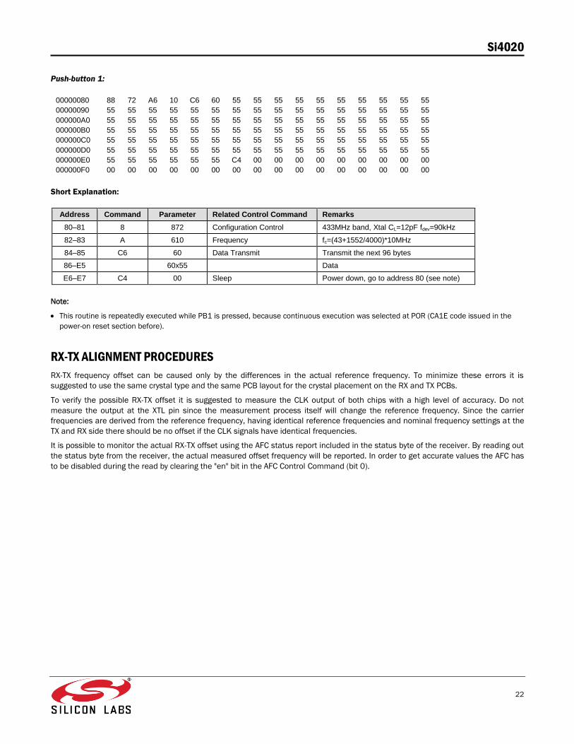
Push-button 1:
00000080 88 72 A6 10 C6 60 55 55 55 55 55 55 55 55 55 55
00000090 55 55 55 55 55 55 55 55 55 55 55 55 55 55 55 55
000000A0 55 55 55 55 55 55 55 55 55 55 55 55 55 55 55 55
000000B0 55 55 55 55 55 55 55 55 55 55 55 55 55 55 55 55
000000C0 55 55 55 55 55 55 55 55 55 55 55 55 55 55 55 55
000000D0 55 55 55 55 55 55 55 55 55 55 55 55 55 55 55 55
000000E0 55 55 55 55 55 55 C4 00 00 00 00 00 00 00 00 00
000000F0 00 00 00 00 00 00 00 00 00 00 00 00 00 00 00 00
Short Explanation:
Address Command Parameter Related Control Command Remarks
80–81 8 872 Configuration Control 433MHz band, Xtal CL=12pF fdev=90kHz
82–83 A 610 Frequency fc=(43+1552/4000)*10MHz
84–85 C6 60 Data Transmit Transmit the next 96 bytes
86–E5 60x55 Data
E6–E7 C4 00 Sleep Power down, go to address 80 (see note)
Note:
This routine is repeatedly executed while PB1 is pressed, because continuous execution was selected at POR (CA1E code issued in the
power-on reset section before).
RX-TX ALIGNMENT PROCEDURES
RX-TX frequency offset can be caused only by the differences in the actual reference frequency. To minimize these errors it is
suggested to use the same crystal type and the same PCB layout for the crystal placement on the RX and TX PCBs.
To verify the possible RX-TX offset it is suggested to measure the CLK output of both chips with a high level of accuracy. Do not
measure the output at the XTL pin since the measurement process itself will change the reference frequency. Since the carrier
frequencies are derived from the reference frequency, having identical reference frequencies and nominal frequency settings at the
TX and RX side there should be no offset if the CLK signals have identical frequencies.
It is possible to monitor the actual RX-TX offset using the AFC status report included in the status byte of the receiver. By reading out
the status byte from the receiver, the actual measured offset frequency will be reported. In order to get accurate values the AFC has
to be disabled during the read by clearing the "en" bit in the AFC Control Command (bit 0).
Si4020
23
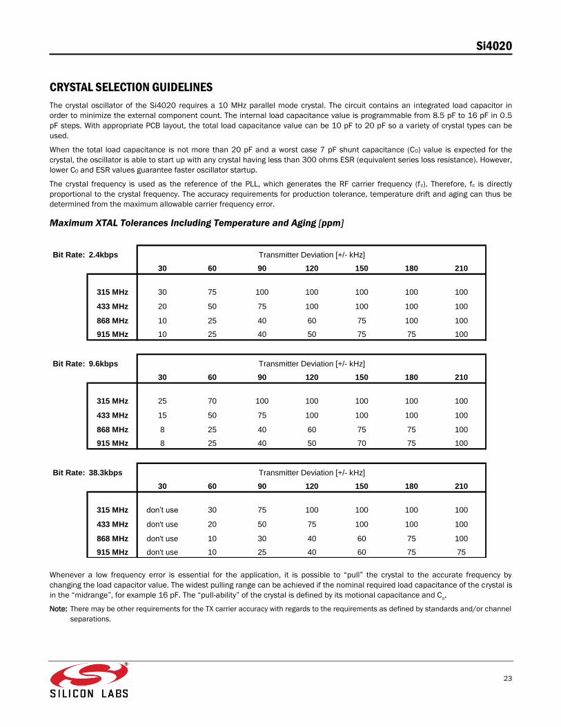
CRYSTAL SELECTION GUIDELINES
The crystal oscillator of the Si4020 requires a 10 MHz parallel mode crystal. The circuit contains an integrated load capacitor in
order to minimize the external component count. The internal load capacitance value is programmable from 8.5 pF to 16 pF in 0.5
pF steps. With appropriate PCB layout, the total load capacitance value can be 10 pF to 20 pF so a variety of crystal types can be
used.
When the total load capacitance is not more than 20 pF and a worst case 7 pF shunt capacitance (C0) value is expected for the
crystal, the oscillator is able to start up with any crystal having less than 300 ohms ESR (equivalent series loss resistance). However,
lower C0 and ESR values guarantee faster oscillator startup.
The crystal frequency is used as the reference of the PLL, which generates the RF carrier frequency (fc). Therefore, fc is directly
proportional to the crystal frequency. The accuracy requirements for production tolerance, temperature drift and aging can thus be
determined from the maximum allowable carrier frequency error.
Maximum XTAL Tolerances Including Temperature and Aging [ppm]
Bit Rate: 2.4kbps
30 60 90 120 150 180 210
315 MHz 30 75 100 100 100 100 100
433 MHz 20 50 75 100 100 100 100
868 MHz 10 25 40 60 75 100 100
915 MHz 10 25 40 50 75 75 100
Bit Rate: 9.6kbps
30 60 90 120 150 180 210
315 MHz 25 70 100 100 100 100 100
433 MHz 15 50 75 100 100 100 100
868 MHz 8 25 40 60 75 75 100
915 MHz 8 25 40 50 70 75 100
Bit Rate: 38.3kbps
30 60 90 120 150 180 210
315 MHz don’t use 30 75 100 100 100 100
433 MHz don't use 20 50 75 100 100 100
868 MHz don't use 10 30 40 60 75 100
915 MHz don't use 10 25 40 60 75 75
Transmitter Deviation [+/- kHz]
Transmitter Deviation [+/- kHz]
Transmitter Deviation [+/- kHz]
Whenever a low frequency error is essential for the application, it is possible to “pull” the crystal to the accurate frequency by
changing the load capacitor value. The widest pulling range can be achieved if the nominal required load capacitance of the crystal is
in the “midrange”, for example 16 pF. The “pull-ability” of the crystal is defined by its motional capacitance and C0.
Note: There may be other requirements for the TX carrier accuracy with regards to the requirements as defined by standards and/or channel
separations.
Si4020
24
RESET MODES
The chip will enter into reset mode if any of the following conditions are met:
Power-on reset: During a power up sequence until the Vdd has reached the correct level and stabilized
Power glitch reset: Transients present on the Vdd line
Software reset: Special control command received by the chip
Power-on reset
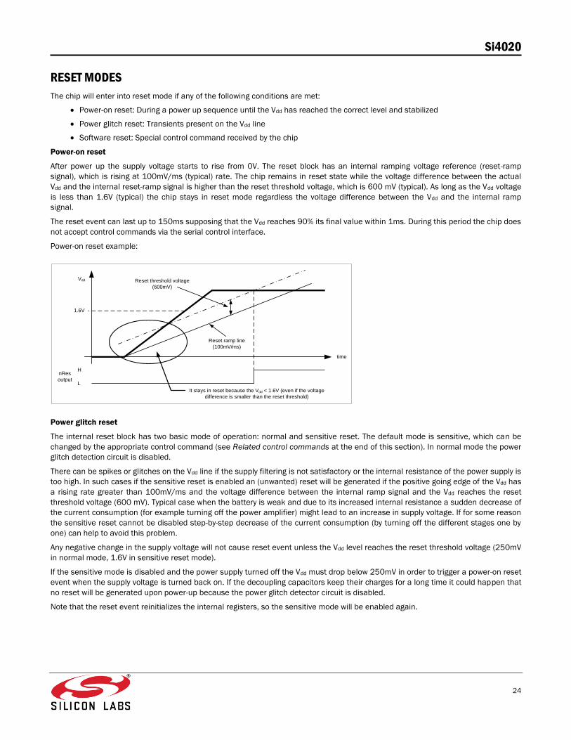
After power up the supply voltage starts to rise from 0V. The reset block has an internal ramping voltage reference (reset-ramp
signal), which is rising at 100mV/ms (typical) rate. The chip remains in reset state while the voltage difference between the actual
Vdd and the internal reset-ramp signal is higher than the reset threshold voltage, which is 600 mV (typical). As long as the Vdd voltage
is less than 1.6V (typical) the chip stays in reset mode regardless the voltage difference between the Vdd and the internal ramp
signal.
The reset event can last up to 150ms supposing that the Vdd reaches 90% its final value within 1ms. During this period the chip does
not accept control commands via the serial control interface.
Power-on reset example:
time
Vdd Reset threshold voltage
(600mV)
nRes
output
H
L
1.6V
It stays in reset because the Vdd < 1.6V (even if the voltage
difference is smaller than the reset threshold)
Reset ramp line
(100mV/ms)
Power glitch reset
The internal reset block has two basic mode of operation: normal and sensitive reset. The default mode is sensitive, which can be
changed by the appropriate control command (see Related control commands at the end of this section). In normal mode the power
glitch detection circuit is disabled.
There can be spikes or glitches on the Vdd line if the supply filtering is not satisfactory or the internal resistance of the power supply is
too high. In such cases if the sensitive reset is enabled an (unwanted) reset will be generated if the positive going edge of the Vdd has
a rising rate greater than 100mV/ms and the voltage difference between the internal ramp signal and the Vdd reaches the reset
threshold voltage (600 mV). Typical case when the battery is weak and due to its increased internal resistance a sudden decrease of
the current consumption (for example turning off the power amplifier) might lead to an increase in supply voltage. If for some reason
the sensitive reset cannot be disabled step-by-step decrease of the current consumption (by turning off the different stages one by
one) can help to avoid this problem.
Any negative change in the supply voltage will not cause reset event unless the Vdd level reaches the reset threshold voltage (250mV
in normal mode, 1.6V in sensitive reset mode).
If the sensitive mode is disabled and the power supply turned off the Vdd must drop below 250mV in order to trigger a power-on reset
event when the supply voltage is turned back on. If the decoupling capacitors keep their charges for a long time it could happen that
no reset will be generated upon power-up because the power glitch detector circuit is disabled.
Note that the reset event reinitializes the internal registers, so the sensitive mode will be enabled again.

Si4020
25
Sensitive Reset Enabled, Ripple on Vdd:
time
Vdd Reset threshold voltage
(600mV)
nRes
output
H
L
1.6V
Reset ramp line
(100mV/ms)
Sensitive reset disabled:
time
Vdd
Reset threshold voltage
(600mV)
nRes
output
H
L
250mV
Reset ramp line
(100mV/ms)
Software reset
Software reset can be issued by sending the appropriate control command (described at the end of the section) to the chip. The
result of the command is the same as if power-on reset was occurred.
Vdd line filtering
During the reset event (caused by power-on, fast positive spike on the supply line or software reset command) it is very important to
keep the Vdd line as smooth as possible. Noise or periodic disturbing signal superimposed the supply voltage may prevent the part
getting out from reset state. To avoid this phenomenon use adequate filtering on the power supply line to keep the level of the
disturbing signal below 10mVp-p in the DC – 50kHz range for 200ms from Vdd ramp start.. Typical example when a switch-mode
regulator is used to supply the radio, switching noise may be present on the Vdd line. Follow the manufacturer’s recommendations
how to decrease the ripple of the regulator IC and/or how to shift the switching frequency.
Related control commands
“Low Battery Detector Command”
Setting bit<6> to high will change the reset mode to normal from the default sensitive.
“SW Reset Command”
Issuing FF00h command will trigger software reset. See the Wake-up Timer Command.

Si4020
26
SIMPLIFIED INTERNAL CONTROL AND TIMING
The internal controller uses the clock generated by the crystal oscillator to sequentially process the various events and to de-bounce
the push-button (PB) inputs. If the oscillator is not running, internal logic automatically turns it on temporarily and then off again.
Such events are: any wake-up event (POR, PB press, wake-up timer timeout, and low supply voltage detection), PB release and
status read request by the microcontroller.
If two wake-up events occur in succession, the crystal oscillator stays on until the next status read (acknowledgment of the first
event).
Simplified Internal Control and Timing Diagrams
Note:
* Tsx : Crystal oscillator st artup t ime
** Length of Tclk_tail is determined by the parameter in the Sleep comm a nd
Vdd
Push-button
inpu t x
Microcontroller mode (ec=0, ex=0)
SPI
Osc_On
(In terna l)
POR
(inte rna l)
Debouncing Time + T sx*
Status rd cmd Status rd cmd
(PB x)
Stat. b its
Vdd
SPI
Osc_On
(In terna l)
POR
(inte rna l)
nIRQ
Status rd cmd
(PO R)
Stat. b its
Status rd cmd
(PB x)
Stat. b its
Microcontroller modewith multiple event read (ec=0, ex=0)
nIRQ
Push-button
inpu t x
1us Tsx*
(PO R)
Stat. b its
Tsx* Tsx*
Vdd
Microcontroller mode (ec=1, ex=0)
SPI
Osc_On
(In terna l)
POR
(inte rna l)
Slee p cmd Slee p cmd
Push-button
inpu t x
Tclk_tail**
Status rd Status rd
Tclk_tail**
Si4020
27
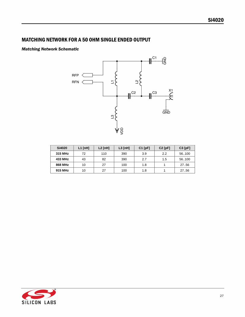
MATCHING NETWORK FOR A 50 OHM SINGLE ENDED OUTPUT
Matching Network Schematic
Si4020 L1 [nH] L2 [nH] L3 [nH] C1 [pF] C2 [pF] C3 [pF]
315 MHz 72 110 390 3.9 2.2 56..100
433 MHz 43 82 390 2.7 1.5 56..100
868 MHz 10 27 100 1.8 1 27..56
915 MHz 10 27 100 1.8 1 27..56
Si4020
28
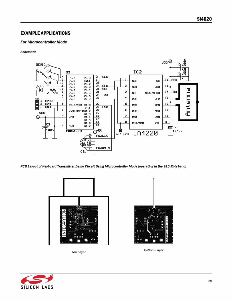
EXAMPLE APPLICATIONS
For Microcontroller Mode
Schematic
PCB Layout of Keyboard Transmitter Demo Circuit Using Microcontroller Mode (operating in the 915 MHz band)
Top Layer
Bottom Layer
Si4020
29
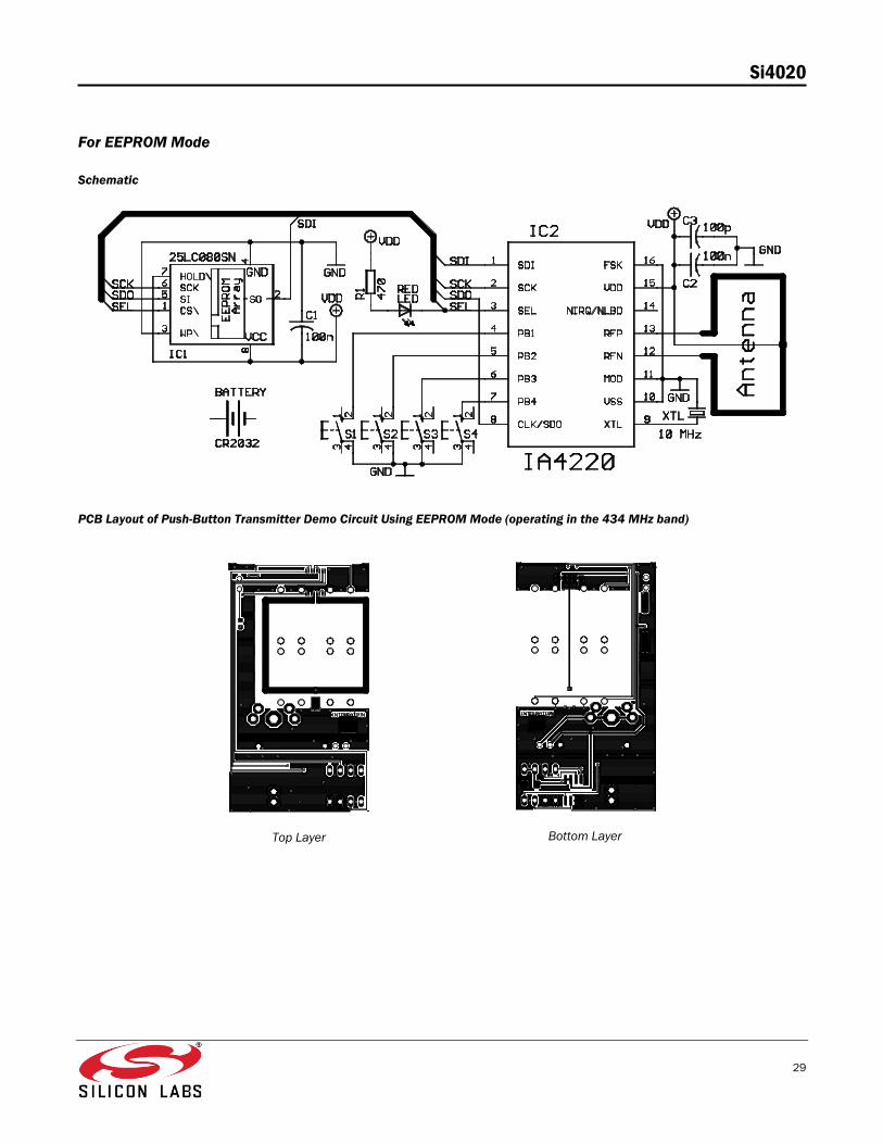
For EEPROM Mode
Schematic
PCB Layout of Push-Button Transmitter Demo Circuit Using EEPROM Mode (operating in the 434 MHz band)
Top Layer
Bottom Layer

Si4020
30
PACKAGE INFORMATION
16-pin TSSOP
Detail “A”
Gauge Plane
0.25
Section B-B
See Detail “A”
Min. Nom. Max. Min. Nom. Max.
740,002,1A
600,0200,051,050,01A
A2 0,80 0,90 1,05 0,031 0,035 0,041
210,0700,003,091,0b
b1 0,19 0,22 0,25 0,007 0,009 0,010
800,0400,002,090,0c
600,0400,061,090,01c
D 4,90 5,00 5,10 0,193 0,197 0,201
e
E
E1 4,30 4,40 4,50 0,169 0,173 0,177
L 0,50 0,60 0,75 0,020 0,024 0,030
L1
400,090,0R
400,090,01R
80801
2
3
SymbolDimensions in mm Dimensions in Inches
.CSB620.0.CSB56.0
6.40 BSC.
12 REF.
12 REF.
12 REF.
12 REF.
1.00 REF.
0.252 BSC.
0.39 REF.
Si4020
31
This page has been intentionally left blank.

Si4020
32
RELATED PRODUCTS AND DOCUMENTS
Si4020 Universal ISM Band FSK Transmitter
DESCRIPTION ORDERING NUMBER
Si4020 16-pin TSSOP Si4020-IC CC16 Rev I1
die see Silicon Labs
Demo Boards and Development Kits
DESCRIPTION ORDERING NUMBER
Development Kit IA ISM – DK
Remote Temperature Monitoring Station IA ISM – DATD
Related Resources
DESCRIPTION ORDERING NUMBER
Antenna Selection Guide IA ISM – AN1
Antenna Development Guide IA ISM – AN2
IA4320 Universal ISM Band FSK Receiver See www.silabs.com/integration for details
Note: Volume orders must include chip revision to be accepted.
Silicon Labs, Inc.
400 West Cesar Chavez
Austin, Texas 78701
Tel: 512.416.8500
Fax: 512.416.9669
Toll Free: 877.444.3032
www.silabs.com/integration
The specifications and descriptions in this document are based on
information available at the time of publication and are subject to change
without notice. Silicon Laboratories assumes no responsibility for errors or
omissions, and disclaims responsibility for any consequences resulting from
the use of information included herein. Additionally, Silicon Laboratories
assumes no responsibility for the functioning of undescribed features or
parameters. Silicon Laboratories reserves the right to make changes to the
product and its documentation at any time. Silicon Laboratories makes no
representations, warranties, or guarantees regarding the suitability of its
products for any particular purpose and does not assume any liability arising
out of the application or use of any product or circuit, and specifically
disclaims any and all liability for consequential or incidental damages arising
out of use or failure of the product. Nothing in this document shall operate
as an express or implied license or indemnity under the intellectual property
rights of Silicon Laboratories or third parties. The products described in this
document are not intended for use in implantation or other direct life support
applications where malfunction may result in the direct physical harm or
injury to persons. NO WARRANTIES OF ANY KIND, INCLUDING BUT NOT
LIMITED TO, THE IMPLIED WARRANTIES OF MERCHANTABILITY OR
FITNESS FOR A PARTICULAR PURPOSE, ARE OFFERED IN THIS
DOCUMENT.
©2008 Silicon Laboratories, Inc. All rights reserved. Silicon Laboratories is a trademark of Silicon
Laboratories, Inc. All other trademarks belong to their respective owners.
W

http://www.silabs.com
Silicon Laboratories Inc.400 West Cesar ChavezAustin, TX 78701USA
Smart.Connected.Energy-Friendly
Productswww.silabs.com/products
Qualitywww.silabs.com/quality
Support and Communitycommunity.silabs.com
DisclaimerSilicon Laboratories intends to provide customers with the latest, accurate, and in-depth documentation of all peripherals and modules available for system and software implementers using or intending to use the Silicon Laboratories products. Characterization data, available modules and peripherals, memory sizes and memory addresses refer to each specific device, and "Typical" parameters provided can and do vary in different applications. Application examples described herein are for illustrative purposes only. Silicon Laboratories reserves the right to make changes without further notice and limitation to product information, specifications, and descriptions herein, and does not give warranties as to the accuracy or completeness of the included information. Silicon Laboratories shall have no liability for the consequences of use of the information supplied herein. This document does not imply or express copyright licenses granted hereunder to design or fabricate any integrated circuits. The products are not designed or authorized to be used within any Life Support System without the specific written consent of Silicon Laboratories. A "Life Support System" is any product or system intended to support or sustain life and/or health, which, if it fails, can be reasonably expected to result in significant personal injury or death. Silicon Laboratories products are not designed or authorized for military applications. Silicon Laboratories products shall under no circumstances be used in weapons of mass destruction including (but not limited to) nuclear, biological or chemical weapons, or missiles capable of delivering such weapons.
Trademark InformationSilicon Laboratories Inc.® , Silicon Laboratories®, Silicon Labs®, SiLabs® and the Silicon Labs logo®, Bluegiga®, Bluegiga Logo®, Clockbuilder®, CMEMS®, DSPLL®, EFM®, EFM32®, EFR, Ember®, Energy Micro, Energy Micro logo and combinations thereof, "the world’s most energy friendly microcontrollers", Ember®, EZLink®, EZRadio®, EZRadioPRO®, Gecko®, ISOmodem®, Precision32®, ProSLIC®, Simplicity Studio®, SiPHY®, Telegesis, the Telegesis Logo®, USBXpress® and others are trademarks or registered trademarks of Silicon Laborato-ries Inc. ARM, CORTEX, Cortex-M3 and THUMB are trademarks or registered trademarks of ARM Holdings. Keil is a registered trademark of ARM Limited. All other products or brand names mentioned herein are trademarks of their respective holders.