series-parallel charge pump conditioning circuits for
TRANSCRIPT
HAL Id: hal-01380378https://hal.archives-ouvertes.fr/hal-01380378
Submitted on 13 Oct 2016
HAL is a multi-disciplinary open accessarchive for the deposit and dissemination of sci-entific research documents, whether they are pub-lished or not. The documents may come fromteaching and research institutions in France orabroad, or from public or private research centers.
L’archive ouverte pluridisciplinaire HAL, estdestinée au dépôt et à la diffusion de documentsscientifiques de niveau recherche, publiés ou non,émanant des établissements d’enseignement et derecherche français ou étrangers, des laboratoirespublics ou privés.
Series-Parallel Charge Pump Conditioning Circuits forElectrostatic Kinetic Energy Harvesting
Armine Karami, Dimitri Galayko, Philippe Basset
To cite this version:Armine Karami, Dimitri Galayko, Philippe Basset. Series-Parallel Charge Pump Conditioning Circuitsfor Electrostatic Kinetic Energy Harvesting. IEEE Transactions on Circuits and Systems Part 1Fundamental Theory and Applications, Institute of Electrical and Electronics Engineers (IEEE), 2017,64 (1), pp.227-240. �10.1109/TCSI.2016.2603064�. �hal-01380378�
IEEE TRANSACTIONS ON CIRCUITS AND SYSTEMS—I: REGULAR PAPERS 1
Series-Parallel Charge Pump Conditioning Circuitsfor Electrostatic Kinetic Energy HarvestingArmine Karami, Student Member, IEEE, Dimitri Galayko, Member, IEEE, and Philippe Basset
Abstract—This paper presents a new family of conditioningcircuits used in electrostatic kinetic energy harvesters (e-KEHs),generalizing a previously reported conditioning circuit knownas the Bennet’s doubler. The proposed topology implements aconditioning scheme described by a rectangular charge-voltagecycle (QV-cycle) of tunable aspect ratio. These circuits show anexponential increase of the converted energy over operation timeif studied in the sole electrical domain. The QV-cycle’s aspect ratiocan be set to values that were previously inaccessible with other ex-ponential conditioning circuits. After a brief intuitive presentationof the new topology, its operation is rigorously analyzed and itsdynamics are quantitatively derived in the electrical domain. Inparticular, the aspect ratio of the rectangular QV-cycle describingthe biasing scheme of the transducer is expressed as a functionof the circuit’s parameters. Practical considerations about the useof the reported conditioning circuits in actual e-KEHs are alsopresented. These include a discussion on the applications of theproposed conditioning, a description of the effects of electricalnonidealities, and a proposition of an energy extracting interface.
Index Terms—Conditioning circuits, electrostatic kinetic energyharvesting, energy conversion, series-parallel charge pumps.
I. INTRODUCTION
CONDITIONING circuits are a critical block of electro-static kinetic energy harvesters (e-KEHs). Indeed, an in-
herent property of the electrostatic transduction mechanism isthat the harvested power depends on the biasing scheme of thetransducer throughout the variation of its capacitance betweentwo extremal values. This biasing scheme depends on the usedconditioning circuit.
Until now, several topologies for e-KEHs conditioning cir-cuits have been studied, realizing different biasing schemes.The requirement for electrical interfaces that are self-synchronized with the external vibrations have legitimated thestudy of a family of “charge-pump” conditioning circuits, e.g.,[1]–[3]. Circuits of this family have the common fundamentalcharacteristic of implementing a rectangular charge-voltagediagram at each cycle of the conditioning circuit’s operation(rectangular QV-cycle) [4]. The QV-cycle is a simple andpowerful geometrical tool that summarizes the evolution of thetransducer’s biasing and charge during a cycle of its capacitancevariation [5], [6]. It gives a quick estimation of the convertedenergy per cycle, which is equal to the area enclosed by thetransducer’s QV curve.
Manuscript received April 16, 2016; revised August 7, 2016; acceptedAugust 21, 2016. This paper was recommended by Associate EditorN. Krishnapura.
A. Karami and D. Galayko are with Sorbonne Universités, UPMC Univ Paris06, UMR 7606, LIP6, F-75005 Paris, France (e-mail: [email protected]).
P. Basset is with Université Paris-Est, ESYCOM, ESIEE Paris, France.Digital Object Identifier 10.1109/TCSI.2016.2603064
As shown in [4], a fundamental characteristic of these charge-pump conditioning circuits is that the amount of convertedenergy at each cycle of the capacitance variation is a functionof the internal energy in the circuit and of the transducercapacitance variation.
All the cited charge-pump conditioning circuits exhibit anoptimal cycle in terms of the harvested energy per cycle (thatwill be referred to as harvested power in the rest of the pa-per). With these circuits, the harvested power is fundamentallylimited by the transducer’s capacitance variation and the initialenergy stored in the circuit. Moreover, under autonomous oper-ation of the circuit submitted to a variation of the transducer’scapacitance, the harvested energy is reinvested in the circuit,changing the harvested energy at the next cycle. Notably, afterreaching an eventual maximum in the harvested power, theconverted energy per cycle of the capacitance variation tendsto zero, i.e., the QV-cycle degenerates into an horizontal line.
In [7], De Queiroz et al. present a new circuit of the charge-pump conditioning family, that is referred to in the literatureas the “Bennet’s doubler,” as it is derived from an electrostaticmachine first described by Bennet et al. in the 18th century [8].This charge-pump conditioning circuit has the major advantageof exhibiting an operation mode in which the harvested power isexponentially growing, and a fortiori non-saturating, as long asthe electromechanical coupling is not taken into account. Thisexponential growth starts from an arbitrarily low initial energyin the system.
In the present paper, a new generic conditioning circuittopology, based on a series-parallel charge pump topology, ispresented and rigorously analyzed in the electrical domain. Thistopology is shown to be a generalization of the Bennet’s dou-bler, uncovering an entire new family of conditioning circuits.The full rigorous analysis of the Bennet’s doubler is hence con-tained in the presented analysis. This generic topology allowsthe realization of different biasing schemes of the transducerat the scale of one cycle of the transducer’s capacitance vari-ation (i.e., different QV-cycles), with long-term autonomousexponential increase of the harvested power. The proof of theexponential operation mode and the quantitative derivation ofthe associated QV-cycle’s geometric properties is the subject ofthe analysis. As it is discussed in the final part of the paper, thisvariety of conditioning schemes can be of interest, for examplein the case of electret e-KEHs, or to optimize the device’soperation under the impact of the electromechanical coupling,that is dependent on the biasing scheme implemented at eachcycle of the transducer’s capacitance variation.
The plan of the paper is as follows. In Section II, a simplifiedand intuitive way to describe the original Bennet’s doublercircuit is presented, and based on this view of the circuit, thegeneric circuit topology is naturally deduced. In Sections III
1549-8328 © 2016 IEEE. Personal use is permitted, but republication/redistribution requires IEEE permission.See http://www.ieee.org/publications_standards/publications/rights/index.html for more information.

2 IEEE TRANSACTIONS ON CIRCUITS AND SYSTEMS—I: REGULAR PAPERS
Fig. 1. Different representations of the Bennet’s doubler circuit. The originalrepresentation is depicted in (a). The topology as represented in (b) has beenproposed in [9]. The reasoning in the present work is based on the circuit viewedas in (c).
Fig. 2. QV-cycle for an e-KEH with a charge pump conditioning circuit thatimplements a fixed ratio q between the voltages biasing the transducer at itsextremal capacitance values.
and IV, the topology is formally analyzed to quantitativelydescribe the circuit’s dynamics and its different operationregimes, submitted to a periodic variation of the transducer’scapacitance. Finally, considerations about the practical use ofthis circuit in an e-KEH context are discussed in Section V: theQV-cycle of the circuit is derived, motivations for the use ofthe presented topology are given, and generic energy extractinginterfaces are discussed.
II. PRESENTATION OF THE CIRCUIT
The original Bennet’s doubler conditioning circuit is de-picted in Fig. 1(a). The variable capacitor Cvar models thetransducer electrically, and is varying over time between fixedmaximal and minimal values (not necessarily periodically).Note that, as the paper deals with the analysis in the sole elec-trical domain, Cvar is considered in this study as an unalterableinput. The biasing scheme implemented by this circuit, in thesteady-state regime, is such that the e-KEH has the propertyof control-less exponential increase of the harvested power,as discussed in the introduction. This is true as long as theratio between maximal and minimal capacitance values is largerthan 2. This exponential increase and the condition on thetransducer’s extremal capacitance values are fundamentally dueto the rectangular QV-cycle of the circuit which exhibits a fixedratio of 2 between the extreme voltages across the transducer atthe scale at one cycle throughout the circuit’s operation. At anycycle of its operation in the exponential steady-state mode, theQV-cycle of the Bennet’s doubler circuit is therefore as depictedin Fig. 2, with q = 2.
In [9], Lefeuvre et al. have proposed to view the Bennet’sdoubler conditioning circuit as a voltage doubling cell, asdepicted in Fig. 1(b), to which a flyback diode is added be-tween the output capacitor and the variable capacitor. From this
Fig. 3. The proposed generic topology for series-parallel charge-pump condi-tioning circuits of e-KEHs.
representation of the circuit, it comes that adding Cockcroft-Walton multiplier cells in the flyback enables to modulate thebiasing of the circuit’s capacitors, as explained in [10]. Thisis the first generalization of the Bennet’s circuit. Indeed, itshows the same control-less exponentially-growing voltage inits steady-state operation regime, as it implements at each cycleof the capacitance variation, an extreme voltage ratio tending toq, which is such that 1 < q = (K + 1)/K ≤ 2,K ∈ N
∗, whereK is the number of multiplier cells in the flyback.
In the present paper, to have a grasp of its operation principle,it is proposed to first view the Bennet’s doubler circuit asa series-parallel voltage multiplier, driven by an alternatingcurrent source modeling the transducer, as depicted in Fig. 1(c).The circuit cyclically alternates between two phases of positiveand negative current. In phase (i), the current is positive andthe fixed capacitors of the network are in series through Ds. Atthe end of this phase each one of the capacitors has receiveda charge δQ. In phase (ii), the current is negative, and thefixed capacitors of the network are in parallel with the currentsource through Dp1
and Dp2. The total charge given back to the
current source is equal to δQ. Thus, at the end of the cycle, thetotal charge in the fixed capacitors C1, C2 has increased of δQ.Consequently, the system’s total energy has increased. If theratio between δQ and the total charge in the circuit’s capacitorsat the beginning of the corresponding cycle is fixed throughoutthe circuit’s operation, then the system’s total energy increasesexponentially over the cycles.
Viewing the variable capacitor as a voltage or a currentsource driving the fixed capacitor network only serves as an in-tuitive description of the circuit’s operation based on traditionalwidely-used series-parallel switched capacitors networks. Inpoint of fact, it is necessary to describe the transducer’s biasingevolution locally across one cycle of the capacitance variation(e.g., in terms of its QV-cycle) to derive the resulting long-termdynamics of the circuit, and to identify its different operationregimes. Therefore, a rigorous analysis has to be carried outreplacing the current source by the transducer’s variable capaci-tor,Cvar. The fundamental law Qvar=VvarCvar, is then respon-sible for the circuit’s dynamics subsequent to Cvar’s variation.
The generic series-parallel conditioning circuit topology pro-posed in this paper is depicted in Fig. 3. It is a natural gener-alization of the circuit represented in Fig. 1(c) to a number offixed capacitors branches greater than 2. It is shown in the restof the paper that at the scale of one cycle, the extremal values ofthe bias across the transducer have a fixed ratio equal to somerational q, that is set by the choice of the circuit’s elements. Theimplemented QV-cycle is depicted in Fig. 2. In this mode, theharvested power increases exponentially.
The two next sections go through a full and rigorous analysisof the circuit’s operation. The conditions for the circuit to
KARAMI et al.: SERIES-PARALLEL CHARGE PUMP CONDITIONING CIRCUITS FOR ELECTROSTATIC KINETIC ENERGY HARVESTING 3
operate in the exponential mode, and the relations between theparameters and the circuit’s dynamics, are derived. This oper-ation mode is the most advantageous in the electrical domain,as it allows to reach high energy conversion rates, instead of aconverted energy tending to zero for long times for saturatingmodes. The different possible steady-state operation regimesof the generic circuit are described. Note that, in the process,this completes the analysis of the Bennet’s doubler, which isa particular case of the generic topology, for which only theexponential regime has been studied so far.
III. LOCAL EVOLUTION LAWS
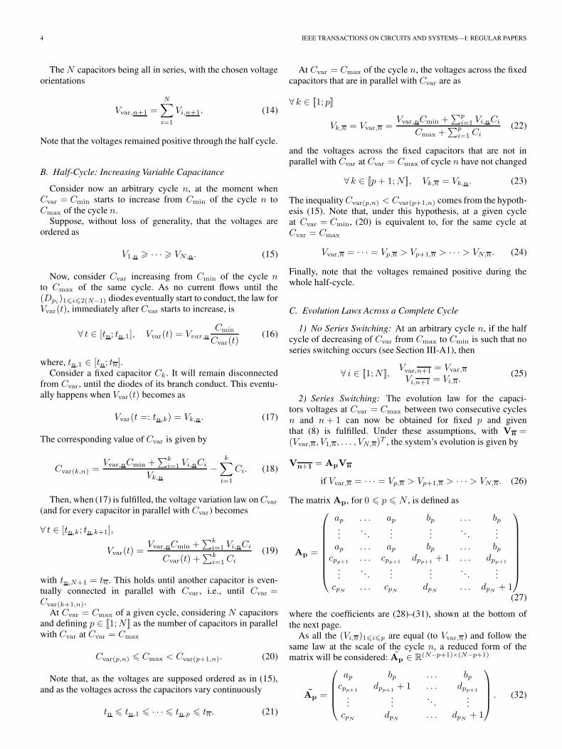
The following analysis of the circuit’s dynamics presumesthat Cvar is monotonously varying between fixed minimum andmaximum, that will be denoted Cmin and Cmax, respectively(Cmax > Cmin). The parameter η is defined as:
η = Cmax/Cmin. (1)
A cycle is defined as a variation of Cvar between a localmaximum or minimum to the following local maximum or min-imum. The purpose of this subsection is to give the evolutionlaw of the circuit’s capacitors voltages from an arbitrary cycleto the next.
The voltage across Cvar will be denoted Vvar,n at a cycle nwhen Cvar = Cmax, Vvar,n at a cycle n when Cvar = Cmin, andVvar(t) at any time t. Similarly, the voltage across a capacitorCi, i ∈ [[1;N ]], will be denoted Vi,n at a cycle n when Cvar =Cmax, Vk,n at a cycle n when Cvar = Cmin, and Vi(t) at a anytime t.
The chosen convention for the chronology is such thatCvar = Cmin at the cycle n, then Cvar = Cmax at the cycle n,then Cvar = Cmin at the cycle n+ 1, and so on. Also, tn denotethe time when at cycle n, Cvar = Cmax and tn denotes the timewhen at cycle n, Cvar = Cmin. Thus, tn < tn < tn+1 < tn+1.The cycle indexes are chosen as integers, the beginning of timeis noted t0.
All the circuit elements are considered ideal. In particular,the diode elements follow the ideal diode current-voltage law,with a zero threshold voltage.
Let’s immediately note that, from the circuit topology
∀ t � t0, ∀ i ∈ [[1;N ]], Vi(t) � Vvar(t) �N∑j=1
Vj(t). (2)
A. Half-Cycle: Decreasing Variable Capacitance
Let’s consider an arbitrary cycle n, at the moment when Cvar
starts to decrease from Cmax of the previous cycle n, to Cmin
of the cycle n+ 1.Suppose that
Vvar,n>0, ∃j ∈ [[1;N ]], Vj,n > 0, ∀ i ∈ [[1;N ]], Vi,n � 0. (3)
As no current flows until a subset of the (Dsi)1�i�N−1
diodes conduct, the law for Vvar(t), immediately after Cvar
starts to decrease, is, for a certain tn,s ∈ [tn; tn+1]
∀ t ∈ [tn; tn,s], Vvar(t) = Vvar,nCmax
Cvar(t)(4)
and the voltage across the fixed capacitors remains constant
∀ i ∈ [[1;N ]], ∀ t ∈ [tn; tn,s], Vi(t) = Vi,n. (5)
1) No Series Switching: If the diodes (Dsi)1�i�N−1 do notconduct for any t ∈ [tn; tn+1[ then tn,s = tn+1, and the voltageacross Cvar at the end of the half-cycle is
Vvar,n+1 = ηVvar,n. (6)
The voltage across the fixed capacitors at the end of the half-cycle is
∀ i ∈ [[1;N ]], Vi,n = Vi,n+1. (7)
2) Series Switching: Otherwise, the circuit will switch to itsseries configuration when the voltage across Cvar makes the(Dsi)1�i�N−1 diodes conduct. This happens when
Vvar(t =: tn,s) =
N∑i=1
Vi,n (8)
and the corresponding value of Cvar is
Cvar =Vvar,n∑Ni=1 Vi,n
Cmax. (9)
The circuit is then equivalent to Cvar being in series with acapacitor of value C = 1/(
∑Ni=1 Ci
−1). The voltage variationlaw on Cvar becomes
∀ t ∈ [tn,s; tn+1]
Vvar(t) =
N∑i=1
Vi(t) =
N∑i=1
Vi,n +ΔQn(t)
N∑i=1
Ci−1 (10)
where
∀ t ∈ [tn,s; tn+1]
ΔQn(t) =Vvar,nCmax − Cvar(t)
∑Ni=1 Vi,n
1 + Cvar(t)∑N
i=1 Ci−1
. (11)
If the circuit has entered its series configuration beforeCvar=Cmin, the capacitors voltages when Cvar = Cmin satisfy
∀ i ∈ [[1;N ]], Vi,n+1 = Vi,n +ΔQn
Ci(12)
where ΔQn is the amount of charges given by Cvar to theother capacitors, from Cvar = Cmax to Cvar = Cmin. For everycapacitor of the loop, this amount is equal to
ΔQn = CminηVvar,n −
∑Ni=1 Vi,n
1 + Cmin
∑Ni=1 Ci
−1. (13)
Note that ΔQn > 0 as the quantity in (9) is larger than Cmin bythe series switching hypothesis.
4 IEEE TRANSACTIONS ON CIRCUITS AND SYSTEMS—I: REGULAR PAPERS
The N capacitors being all in series, with the chosen voltageorientations
Vvar,n+1 =
N∑i=1
Vi,n+1. (14)
Note that the voltages remained positive through the half cycle.
B. Half-Cycle: Increasing Variable Capacitance
Consider now an arbitrary cycle n, at the moment whenCvar = Cmin starts to increase from Cmin of the cycle n toCmax of the cycle n.
Suppose, without loss of generality, that the voltages areordered as
V1,n � · · · � VN,n. (15)
Now, consider Cvar increasing from Cmin of the cycle nto Cmax of the same cycle. As no current flows until the(Dpi
)1�i�2(N−1) diodes eventually start to conduct, the law forVvar(t), immediately after Cvar starts to increase, is
∀ t ∈ [tn; tn,1], Vvar(t) = Vvar,nCmin
Cvar(t)(16)
where, tn,1 ∈ [tn; tn].Consider a fixed capacitor Ck. It will remain disconnected
from Cvar, until the diodes of its branch conduct. This eventu-ally happens when Vvar(t) becomes as
Vvar(t =: tn,k) = Vk,n. (17)
The corresponding value of Cvar is given by
Cvar(k,n) =Vvar,nCmin +
∑ki=1 Vi,nCi
Vk,n−
k∑i=1
Ci. (18)
Then, when (17) is fulfilled, the voltage variation law on Cvar
(and for every capacitor in parallel with Cvar) becomes
∀ t ∈ [tn,k; tn,k+1],
Vvar(t) =Vvar,nCmin +
∑ki=1 Vi,nCi
Cvar(t) +∑k
i=1 Ci
(19)
with tn,N+1 = tn. This holds until another capacitor is even-tually connected in parallel with Cvar, i.e., until Cvar =Cvar(k+1,n).
At Cvar = Cmax of a given cycle, considering N capacitorsand defining p ∈ [[1;N ]] as the number of capacitors in parallelwith Cvar at Cvar = Cmax
Cvar(p,n) � Cmax < Cvar(p+1,n). (20)
Note that, as the voltages are supposed ordered as in (15),and as the voltages across the capacitors vary continuously
tn � tn,1 � · · · � tn,p � tn. (21)
At Cvar = Cmax of the cycle n, the voltages across the fixedcapacitors that are in parallel with Cvar are as
∀ k ∈ [[1; p]]
Vk,n = Vvar,n =Vvar,nCmin +
∑pi=1 Vi,nCi
Cmax +∑p
i=1 Ci(22)
and the voltages across the fixed capacitors that are not inparallel with Cvar at Cvar = Cmax of cycle n have not changed
∀ k ∈ [[p+ 1;N ]], Vk,n = Vk,n. (23)
The inequalityCvar(p,n) < Cvar(p+1,n) comes from the hypoth-esis (15). Note that, under this hypothesis, at a given cycleat Cvar = Cmin, (20) is equivalent to, for the same cycle atCvar = Cmax
Vvar,n = · · · = Vp,n > Vp+1,n > · · · > VN,n. (24)
Finally, note that the voltages remained positive during thewhole half-cycle.
C. Evolution Laws Across a Complete Cycle
1) No Series Switching: At an arbitrary cycle n, if the halfcycle of decreasing of Cvar from Cmax to Cmin is such that noseries switching occurs (see Section III-A1), then
∀ i ∈ [[1;N ]],Vvar,n+1 = Vvar,n
Vi,n+1 = Vi,n.(25)
2) Series Switching: The evolution law for the capaci-tors voltages at Cvar = Cmax between two consecutive cyclesn and n+ 1 can now be obtained for fixed p and giventhat (8) is fulfilled. Under these assumptions, with Vn =(Vvar,n, V1,n, . . . , VN,n)
T , the system’s evolution is given by
Vn+1 = ApVn
if Vvar,n = · · · = Vp,n > Vp+1,n > · · · > VN,n. (26)
The matrix Ap, for 0 � p � N , is defined as
Ap =
⎛⎜⎜⎜⎜⎜⎜⎜⎜⎝
ap . . . ap bp . . . bp...
. . ....
.... . .
...ap . . . ap bp . . . bp
cpp+1. . . cpp+1
dpp+1+ 1 . . . dpp+1
.... . .
......
. . ....
cpN. . . cpN
dpN. . . dpN
+ 1
⎞⎟⎟⎟⎟⎟⎟⎟⎟⎠(27)
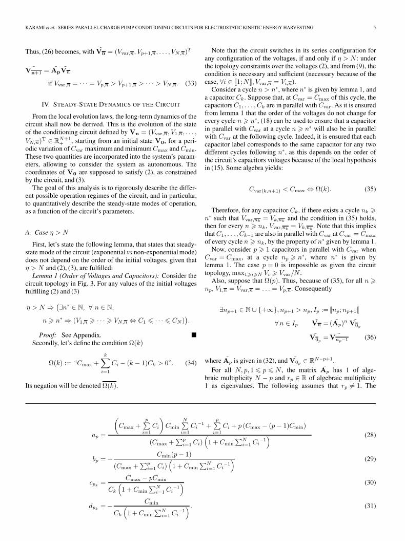
where the coefficients are (28)–(31), shown at the bottom ofthe next page.
As all the (Vi,n)1�i�p are equal (to Vvar,n) and follow thesame law at the scale of the cycle n, a reduced form of thematrix will be considered: Ap ∈ R
(N−p+1)×(N−p+1)
Ap =
⎛⎜⎜⎜⎝
ap bp . . . bpcpp+1
dpp+1+ 1 . . . dpp+1
......
. . ....
cpNdpN
. . . dpN+ 1
⎞⎟⎟⎟⎠ . (32)
KARAMI et al.: SERIES-PARALLEL CHARGE PUMP CONDITIONING CIRCUITS FOR ELECTROSTATIC KINETIC ENERGY HARVESTING 5
Thus, (26) becomes, with Vn = (Vvar,n, Vp+1,n, . . . , VN,n)T
˜Vn+1 = ApVn
if Vvar,n = · · · = Vp,n > Vp+1,n > · · · > VN,n. (33)
IV. STEADY-STATE DYNAMICS OF THE CIRCUIT
From the local evolution laws, the long-term dynamics of thecircuit shall now be derived. This is the evolution of the stateof the conditioning circuit defined by Vn = (Vvar,n, V1,n, . . . ,
VN,n)T ∈ R
N+1+ , starting from an initial state V0, for a peri-
odic variation of Cvar maximum and minimumCmax and Cmin.These two quantities are incorporated into the system’s param-eters, allowing to consider the system as autonomous. Thecoordinates of V0 are supposed to satisfy (2), as constrainedby the circuit, and (3).
The goal of this analysis is to rigorously describe the differ-ent possible operation regimes of the circuit, and in particular,to quantitatively describe the steady-state modes of operation,as a function of the circuit’s parameters.
A. Case η > N
First, let’s state the following lemma, that states that steady-state mode of the circuit (exponential vs non-exponential mode)does not depend on the order of the initial voltages, given thatη > N and (2), (3), are fulfilled:
Lemma 1 (Order of Voltages and Capacitors): Consider thecircuit topology in Fig. 3. For any values of the initial voltagesfulfilling (2) and (3)
η > N ⇒(∃n∗ ∈ N, ∀ n ∈ N,
n � n∗ ⇒ (V1,n � · · · � VN,n ⇔ C1 � · · · � CN )).
Proof: See Appendix. �Secondly, let’s define the condition Ω(k)
Ω(k) := “Cmax +
k∑i=1
Ci − (k − 1)Ck > 0”. (34)
Its negation will be denoted Ω(k).
Note that the circuit switches in its series configuration forany configuration of the voltages, if and only if η > N : underthe topology constraints over the voltages (2), and from (9), thecondition is necessary and sufficient (necessary because of thecase, ∀i ∈ [[1;N ]], Vvar,n = Vi,n).
Consider a cycle n > n∗, where n∗ is given by lemma 1, anda capacitor Ck. Suppose that, at Cvar = Cmax of this cycle, thecapacitors C1, . . . , Ck are in parallel with Cvar. As it is ensuredfrom lemma 1 that the order of the voltages do not change forevery cycle n � n∗, (18) can be used to ensure that a capacitorin parallel with Cvar at a cycle n � n∗ will also be in parallelwith Cvar at the following cycle. Indeed, it is ensured that eachcapacitor label corresponds to the same capacitor for any twodifferent cycles following n∗, as this depends on the order ofthe circuit’s capacitors voltages because of the local hypothesisin (15). Some algebra yields:
Cvar(k,n+1) < Cmax ⇔ Ω(k). (35)
Therefore, for any capacitor Ck, if there exists a cycle nk �n∗ such that Vvar,nk
= Vk,nkand the condition in (35) holds,
then for every n � nk, Vvar,nk= Vk,nk
. Note that this impliesthat C1, . . . , Ck−1 are also in parallel with Cvar at Cvar = Cmax
of every cycle n � nk, by the property of n∗ given by lemma 1.Now, consider p � 1 capacitors in parallel with Cvar when
Cvar = Cmax, at a cycle np � n∗, where n∗ is given bylemma 1. The case p = 0 is impossible as given the circuittopology, max1�i�N Vi � Vvar/N .
Also, suppose that Ω(p). Thus, because of (35), for all n �np, V1,n = Vvar,n = . . . = Vp,n. Consequently
∃np+1 ∈ N ∪ {+∞}, np+1 > np, Ip := [[np;np+1[[
∀n ∈ Ip Vn =(Ap)n V0p
V0p= ˜Vnp−1 (36)
where Ap is given in (32), and V0p ∈ RN−p+1.
For all N, p, 1 � p � N , the matrix Ap has 1 of alge-braic multiplicity N − p and rp ∈ R of algebraic multiplicity1 as eigenvalues. The following assumes that rp �= 1. The
ap =
(Cmax +
p∑i=1
Ci
)Cmin
N∑i=1
Ci−1 +
p∑i=1
Ci + p (Cmax − (p− 1)Cmin)
(Cmax +∑p
i=1 Ci)(1 + Cmin
∑Ni=1 Ci
−1) (28)
bp =− Cmin(p− 1)
(Cmax +∑p
i=1 Ci)(1 + Cmin
∑Ni=1 Ci
−1) (29)
cpk=
Cmax − pCmin
Ck
(1 + Cmin
∑Ni=1 Ci
−1) (30)
dpk=− Cmin
Ck
(1 + Cmin
∑Ni=1 Ci
−1) . (31)
6 IEEE TRANSACTIONS ON CIRCUITS AND SYSTEMS—I: REGULAR PAPERS
eigenvalue 1 has a geometric multiplicity of N − p. Subse-quently, Ap is diagonalizable over R, and it comes that:
Vn =Pp
⎛⎜⎜⎜⎝1
. . .1
rpn
⎞⎟⎟⎟⎠P−1
p V0p(37)
rp=
Cmin
((Cmax+
p∑i=1
Ci
)p∑
i=1
Ci−1+p(η−p+1)
)+
p∑i=1
Ci(1+Cmin
N∑i=1
Ci−1
)(Cmax+
p∑i=1
Ci
)(38)
and where (Pp,Pp−1,V0p
) ∈ (R(N−p+1)2)2 × R(N−p+1).
Hence
Vvar,n =αvar,p rpn + βvar,p
Vk,n =αk,p rpn + βk,p (39)
with (αvar,p, βvar,p, αk,p, βk,p) ∈ R4, and k ∈ [[p+ 1;N ]]. A
simple study of the Ap map allows the derivation of thecoefficients’ expressions; the vectors (vi
1)1�i�N−p, wherevi
1 = (v1i1 , . . . , v1iN−p+1
)T ∈ RN−p+1, are eigenvectors of Ap
associated to the eigenvalue 1
vi1 =1
η − p
vij = δi(j−1), 1 < j � N (40)
where δij is the Kronecker symbol. An eigenvector vrp =(v
rp1 , . . . , v
rpN−p+1)
T ∈ RN−p+1 associated to the eigenvalue
rp is
vrp1 =
(p− 1)CN
Cmax +∑p
i=1 Ci
vrpi =
CN
p− 1 + i, 1 < i � N − p+ 1. (41)
Finally, it comes, (42)–(45), shown at the bottom of the page.The steady-state behavior of the circuit can now readily be
described, that is, the value of p for which Ip = [[n; +∞, andthe long-term voltage evolution laws in this interval. Given thep previously fixed, three cases are discriminated:
1) Case rp > 1: The variations of (Vvar,n − Vp+1,n)n�np,
using the evolution laws of in (37), are such that
(Vvar,n+1 − Vp+1,n+1)− (Vvar,n − Vp+1,n) < 0 ⇔ Ω(p+ 1).(46)
Also, by virtually fixing the law (36) for fixed p, and from (42)and (43)
limn→+∞
Vvar,n
Vp+1,n=
αvar,p
αp+1,p=
(p− 1) Cp+1
Cmax +∑p
i=1 Ci. (47)
In the case Ω(p+ 1), the limit in (47) being then strictly lessthan 1, np+1 < +∞ and Vp+1,np+1
= Vvar,np+1. Because of
(35), ∀n, n � np+1 ⇒ Vvar,n = Vp+1,n. In the case Ω(p+ 1),np+1 = +∞ as the sequence (Vvar,n − Vp+1,n)n�np
is strictlyincreasing. For all k ∈ [[p+ 1;N ]], the asymptotic value of theratio Vvar,n/Vk,n is given by
∀ k ∈ [[p+ 1;N ]]
limn→+∞
Vvar,n
Vk,n=
αvar,p
αk,p=
(p− 1) Ck
Cmax +∑p
i=1 Ci. (48)
αvar,p =
(p− 1)
(N∑
i=p+1
Vi,0p− Vvar,0p
(η − p)
)(Cmax +
p∑i=1
Ci
)N∑
i=p+1
Ci−1 − (p− 1)(η − p)
(42)
αk,p =
(Cmax +
p∑i=1
Ci
)(N∑
i=p+1
Vi,0p− Vvar,0p
(η − p)
)
Ck
((Cmax +
p∑i=1
Ci
)N∑
i=p+1
Ci−1 − (p− 1)(η − p)
) (43)
βvar,p =
(Cmax +
p∑i=1
Ci
)N∑
i=p+1
Ci−1Vvar,0p
− (p− 1)N∑
i=p+1
Vi,0p(Cmax +
p∑i=1
Ci
)N∑
i=p+1
Ci−1 − (p− 1)(η − p)
(44)
βk,p =Vk,0p+
(Cmax +
p∑i=1
Ci
)(Vvar,0p
(η − p)−N∑
i=p+1
Vi,0p
)
Ck
((Cmax +
p∑i=1
Ci
)N∑
i=p+1
Ci−1 − (p− 1)(η − p)
) . (45)
KARAMI et al.: SERIES-PARALLEL CHARGE PUMP CONDITIONING CIRCUITS FOR ELECTROSTATIC KINETIC ENERGY HARVESTING 7
2) Case rp < 1: Note that, from (38), this case happens onlyif Ω(p+ 1). By virtually fixing the law (36)
limn→+∞
Vvar,n = βvar,p, and limn→+∞
Vp+1,n = βp+1,p. (49)
From (44) and (45), some algebra leads to
βp+1,p > βvar,p ⇔ Ω(p+ 1). (50)
Subsequently, np+1 < +∞ and Vp+1,np+1= Vvar,np+1
3) Case rp = 1: In this case, the reduction done in (37) nolonger holds, as the linear map Ap is no longer diagonaliz-able. The voltages increase in this case is linear. This can beseen from the Jordan reduction of Ap, that leads to Ap
n=
Pp′(IN−P+1 +N)Pp
′−1V0p
, where IN−P+1 ∈ R(N−P+1)2
is the identity matrix, Pp′ ∈ R
(N−P+1)2 is invertible and Nhas all its coefficients equal to zero except for N2,1 = n. Thiscase is supposed to not happen in the rest of the analysis, asrp = 1 will never be exactly reached in practice.
4) Summary: The steady-state mode of operation underthe condition η > N can now be defined. This is done byinductively applying the previous reasoning to p+ 1 parallelcapacitors with Ω(p) being fulfilled, starting from the smallestp such that there exists a cycle following n∗ where p capacitorsare in parallel at the same cycle, and Ω(p+ 1) is fulfilled ( Ω(2)is always fulfilled and p � 1). Defining Π as
Π := min({
p ∈]]1;N [[| Ω(p+ 1)}∪ {N}
)(51)
the steady-state mode is defined as the circuit’s operationregime where the biasing of Cvar is implemented in the fol-lowing fashion:
• Cvar is in parallel with the capacitors C1, . . . , CΠ atCvar = Cmax of every cycle, i.e., Vvar,n = V1,n = · · · =VΠ,n.
• The voltage across the capacitor Ci, i ∈ [[Π + 1;N ]] atCvar = Cmax is such that the ratio Vvar,n/Vi,n tends to(Π− 1)Ci/(Cmax +
∑Πj=1 Cj).
• Cvar is in series with all the fixed capacitors C1, . . . , CN
at Cvar = Cmin. Hence, Cvar is biased by the sum ofvoltages across the fixed capacitors at Cvar = Cmin.
The time evolution of the voltages across the fixed capacitorsCvar exhibits an exponential increase in this mode. Indeed,the voltages follow an arithmetico-geometric progression withcommon ratio rΠ > 1 in the steady-state mode.
The ratio q between the voltages at Cvar = Cmax of cyclen and Cvar = Cmin of cycle n+ 1 in the steady-state mode ofoperation is given by
q =
Π+Cmax+
Π∑i=1
Ci
Π−1
N∑i=Π+1
Ci−1 + Cmax
N∑i=1
Ci−1
1 + Cmin
N∑i=1
Ci−1
. (52)
Note that, in the case Π �= N , this ratio is attained asymptot-ically as it is the result of a limit process [see (48)]. Also,this expression can be simplified at the cost of some justifiedapproximations (see (65) below).
The converted energy during a cycle n of the steady-stateoperation defined above is obviously given by
ΔWn =1
2
(Cmax
(Vvar,n+1
2 − Vvar,n2)
+
N∑i=1
Ci
(Vi,n+1
2 − Vi,n2))
. (53)
Again, the full expression is cumbersome, and the use of theQV-cycle in Section V-A will greatly simplify the expression ofconverted power (66).
Remark: The circuit’s dynamics were derived for the steady-state operation mode, irrespective of the initial configuration(this is the purpose of lemma 1). In this process, the piecewisedefined transient mode is described: for each region of thedefinition, the explicit evolution follows the laws given in (39),with proper corresponding values of coefficients αi,j and βi,j
[see (42)–(45)]. However, because of this piecewise definition,there is no simple way to derive the explicit evolution lawsstarting from initial voltage values that do not necessarily fulfillthe order in (15), other than applying the evolution law thatapply in each region, and checking for the intersections ofvoltage in the time domain that lead to a change of the definitionregion.
B. Case η � N
In this case, the condition of series switching at every cycleof the autonomous evolution is not necessarily verified. As aconsequence, the lemma 1 does not necessarily hold, and thelong-term evolution of the circuit’s state depends not only onthe values of the capacitors, but also on their initial voltages.
Because of that, to simplify the analysis, only the dynam-ics starting from a particular order of the circuit’s capacitorsvoltages at the initial cycle will be considered. This particularconfiguration is the same as in the conclusion of lemma 1. Asa matter of fact, Section V-D will highlight that the energyextraction mechanism can be designed in such a way that thisparticular configuration frequently occurs during the system’soperation (see the role of the diode DB in Fig. 6, explained inSection V-D).
Consider an arbitrary cycle n0, chosen as the initial cycle.Consider that the conditions (2), (3) hold. The capacitors arelabeled such that C1 � · · · � CN . The circuit’s capacitors volt-ages are supposed to verify
Vvar,n0= V1,n0
� · · · � VN,n0. (54)
If the initial voltages on the capacitors verify
ηVvar,n0>
N∑i=1
Vi,n0(55)
then it can be verified by induction, using local laws ofSection III, that the circuit switches in series for all cyclesfollowing n0. Otherwise, the circuit shows the trivial dynamicsof (25). The following supposes that (55) is fulfilled. By avariation of the lemma 1, and given the supposed order of thecapacitors, the voltage ordering in (15) does not change forany n � n0. Indeed, this is the case (b.1) in the proof (see

8 IEEE TRANSACTIONS ON CIRCUITS AND SYSTEMS—I: REGULAR PAPERS
Appendix), but using the positivity of the expression (70), asit is sufficient to conclude, instead of the divergence to +∞ ofthe series.
Also, let’s define Ψ(k) as
Ψ(k) := “η − (k − 1)− Ck
N∑i=k
Ci−1 > 0”. (56)
Its negation will be denoted Ψ(k).Consider p � 1 capacitors in parallel at cycle np > n0, and
Ω(p) is fulfilled. As (55) guarantees series switching at allcycles, and similarly to the case η > N [see (35)]
∃np+1 ∈ N ∪ {+∞}, np+1 > np, Ip := [[np;np+1[[
∀n ∈ Ip Vn =(Ap)n V0p
V0p= ˜Vnp−1 (57)
i.e., the evolution laws derived in Section IV-A given in (39) canbe used in this interval.
1) Case rp > 1: In this case, the conclusion is the same asin the rp > 1 case of the analysis for η > N , in Section IV-A. Arefinement of the latter case has to be used to infer conclusionsin the summary: if Ω(p+1) in addition of rp>1, then rp+1>1.
2) Case rp < 1: By virtually fixing the law (57)
limn→+∞
Vvar,n = βvar,p, and limn→+∞
Vp+1,n = βp+1,p. (58)
Also, some algebra yields
∀ i, p ∈ [[1;N ]], βvar,p < βp+1,p ⇔ Ψ(p+ 1). (59)
Thus, if Ψ(p+ 1), then np+1 = +∞ and the voltages saturatefollowing (58). Otherwise, np+1 < +∞, and Ω(p+ 1) holds,as it is implied by rp < 1 and Ψ(p+ 1).
3) Summary: As for the case η > N in Section IV-A, in-ductively, the steady-state regime of the circuit can be char-acterized. As Ψ(p+ 1) ⇒ Ψ(p), if there exists p ∈]]1; �η−�]]such that rp > 1, and Ψ(p) is verified (�η−� = η − 1 if η ∈N, �η� otherwise), then the steady-state mode is an exponentialmode. It is described as for the case η > N (see the summaryin Section IV-A4), with the following expression Π:
Π := min({
t ∈ [[p; �η−�[[| Ω(t+ 1)})
(60)
In particular, if operating in the exponential mode, the ratiobetween the transducer’s extreme voltages across one cycle ofoperation is given by (52), with the parameter Π computedfrom (60).
Otherwise, if rp < 1 for all p, or if Ψ(p) holds for all p, thenthe steady-state mode is a saturation regime,
Remark: This analysis refines the case η > N , as η > N ⇒,∀ p,Ψ(p).
Example (Bennet’s Doubler): Let’s investigate the particu-lar case of the Bennet’s doubler (N = 2), when η � 2, withVvar,n0
= V1,n0> V2,n0
, and supposing that (55) is fulfilled.As r1 < 1, limn→+∞ V2,n = β2,1. Defining σ as
σ :=Vvar,n0
(η − 1)
Vvar,n0(η − 1)− V2,n0
(61)
Fig. 4. The QV-cycle, for the generic circuit topology depicted in Fig. 3, asderived in Section V-A.
if σ < 1 + r1, then an optimal cycle of index nopt > n0 exists
nopt0 = n0 +
⌊log(σ)− log(1 + r1)
log(r1)
⌋. (62)
Otherwise, nopt0 = n0. These are simply found by solving forn the equation ∂ΔWn/∂n = 0 with ΔWn computed as in (53).
Note that the transient process leading to the exponentialsteady-state mode of the Bennet’s doubler circuit, when η > 2,can be characterized in a similar way to this example.
V. PRACTICAL CONSIDERATIONS FOR KINETIC
ENERGY HARVESTING
A. Derivation of the Rectangular QV-Cycle
As stated in the introduction and Section II, the QV-cycle di-agram is an intuitive geometrical tool that has been extensivelyused to describe the electrical operation of e-KEHs. It givesa clear view of the evolution of the transducer’s biasing, andallows a quick estimation of the amount of converted energyduring a cycle using simple geometric arguments: the convertedenergy in a given cycle is equal to the area enclosed by the QVloop for this cycle.
In the present subsection, the QV-cycle implemented bythe circuits using the topology in Fig. 3 is sketched. Theapproximations that allow the diagram to be assimilated to therectangular QV-cycle depicted in Fig. 2 are also discussed.
The derivation of the QV-cycle in this section is made underthe condition η > N (or η � N in an exponential steady-state regime), for an arbitrary cycle of the steady-state modeof operation which was defined in Section IV-A4. Note thatthe derivation is made of for Vvar,n/Vi,n considered equal tothe limit (Π− 1)Ci/(Cmax +
∑Πi=1 Ci)), for i ∈]]Π;N ]]. The
constant Π is defined as in (51).1) Exact Derivation: Starting from the point A (see Fig. 4),
with Cvar decreasing from Cvar = Cmax, no current is flowing,and Vvar increases as stated in (4), hence the horizontal segment[AA’] in the QV plane.
When, at each cycle, Vvar(t) reaches the sum of the voltagesacross all the fixed capacitors, a current flows and the variationlaw of Vvar changes accordingly to (10). The equation of thecorresponding segment [A’B] in the QV plane is given by:
Qvar(t) = −Vvar(t)
(N∑i=1
Ci−1
)−1
+
(N∑i=1
Ci−1
)−1
×(Π+
Cmax +∑k
i=1 Ci
Π− 1
N∑i=Π+1
Ci−1
)Vvar,n. (63)

KARAMI et al.: SERIES-PARALLEL CHARGE PUMP CONDITIONING CIRCUITS FOR ELECTROSTATIC KINETIC ENERGY HARVESTING 9
Now, starting from the point B, with Cvar increasing fromCmin, no current is flowing, and Vvar decreases as stated in (16),hence the horizontal segment [BB1] in the QV plane.
When, at each cycle, Vvar(t) reaches the voltage of thesmallest capacitor, a current flows and the law of variation ofVvar changes, as given in (19). This repeatedly occurs with theother fixed capacitors, until Cvar = Cmax.
The equations of the corresponding segments [BjBj+1] inthe QV plane are given by, with j ∈ [[1; k[[
Qvarj (t) =−Vvar(t)
j∑i=1
Ci + Vvar,n
×[Cmax +
j∑i=1
Ci +
(j − 1
)×(
Cmax−Cmin
(Π+
Cmax+∑k
i=1Ci
Π− 1
N∑i=Π+1
Ci−1
))]
(64)
When Cvar = Cmax at the cycle n+ 1, the voltage andcharge coordinates of the point have increased compared toCvar = Cmax at the cycle n (Vvar,n+1 = rΠVvar,n, rΠ > 1).
2) Approximation to a Rectangular QV-Cycle: The equation(63) shows that if Cmin < Cmax � min1�i�N Ci, then thesegment [A’B] can be considered as vertical going throughA’. Also, under the same condition, equation (64) allows thesegment [BA*] to be considered vertical, and going throughA∗ = A as rΠ ≈ 1+.
In light of these considerations, when Cmax is sufficientlysmall compared to the values of the fixed capacitors, the cyclecan be approximated by the ideal rectangular QV-cycle depictedin Fig. 2. The parameter q of the ideal rectangular QV-cycle (seeFig. 2) is expressed as
q = Π+Cmax +
∑Πi=1 Ci
Π− 1
N∑i=Π+1
Ci−1. (65)
This can also be seen algebraically by simplifying (52) withCmax, Cmin small compared to the Ci’s.
The harvested energy per cycle in the steady-state exponen-tial mode can then be approximated by the area of the obtainedrectangle
ΔWn = CminVvar,n2(q − 1)(η − q). (66)
B. Possible Uses of the Proposed Conditioning
1) Electrical Domain: Some possible advantages of condi-tioning circuits with exponential regimes over other charge-pump conditioning circuits for e-KEH have already beendiscussed in the introduction and, for example, in [9] and [11].However, the comparison depends on the application context,defined by the input and the constraints on the system. In thefollowing, an example of a situation is presented, for which itis advantageous to use a circuit showing an exponential regimein which the transducer is biased by extreme voltages of ratiogreater than 2 at each cycle.
The application context is the following: suppose there existsa maximal allowable voltage VM across the transducer, η > N ,
Fig. 5. (a) Electrical model for an electret-charged transducer (b) The effect ofthe electret on a rectangular QV-cycle.
and the transducer is supposed to use of electret charging to pro-vide a built-in polarization of the transducer (see for example[12], [13]), with no external pre-charging of the circuit’s fixedcapacitors. This built-in bias also provides an initial voltage toe-KEHs using a conditioning circuit with exponential voltageincreasing regime, as has been experimentally verified in [14].A simple electrical model of the electret-charged transduceris represented in Fig. 5(a). The conditioning circuit hencebiases the dipole {transducer+ electret}, rather than directlythe transducer. The effect of the electret on the conditioningscheme is summarized by a voltage offset of E, the value of theelectret’s model equivalent voltage source. This is visible on theQV-cycle depicted in Fig. 5(b).
In [4], the optimal rectangular QV-cycle conditioning schemewas derived as a function of η, under the constraint of a fixedmaximal voltage VM . The optimal cycle was shown to be ob-tained with the following optimal biasing: the upper transducerbias voltage is fixed to VM , and the ratio between the upper andlower voltages biasing the transducer across one period of theexternal vibration is:
qopt transducer =2η
η + 1. (67)
In these conditions, to achieve the ratio in (67) between theupper and lower biasing voltages of transducer across the trans-ducer, using an electret, one has to use a circuit with the ratio
qopt transducer+elec =2η(VM − E)
VM (η + 1)− 2Eη(68)
between the extreme voltages biasing the dipole {transducer +electret} throughout each cycle. The ratio in (68) can be greaterthan 2. A circuit derived from the topology proposed in thispaper, with an appropriate choice of the capacitors, can im-plement this biasing scheme. To do so, the fixed capacitorsvalues have to be chosen so to equate (65) with (68) (remindingthat Π depends on the fixed capacitors values, as derived inSection IV-A4 and B3). An external interface has to let thecircuit reach the optimal cycle and then sustain it, as will bediscussed in Section V-D.
Note that in the example presented above, the use of asaturating charge-pump conditioning circuit (e.g., the simplerectifier circuits presented in [13], that are widely used withelectret e-VEHs) instead of the proposed circuit can only becomparatively disadvantageous. Indeed, the absolute maximalharvested power would intrinsically be limited by E and η,because of the saturation phenomenon. This would lead to aninferior or equal maximal harvested power, compared to thecircuit discussed above, which does not exhibit saturation. Forthe exponential conversion mode circuit, a maximal harvestedpower only exists because of the maximal voltage constraint,
10 IEEE TRANSACTIONS ON CIRCUITS AND SYSTEMS—I: REGULAR PAPERS
provided that η is such that the circuit is in its steady-stateexponential regime.
2) Complete System’s Dynamics: Electro-Mechanically-Coupled Case: Note that in real e-KEHs, the electromechanicalcoupling drastically impacts the dynamics of the whole system({electrical + mechanical}), whereas in the present study, Cvar
has been considered as an unalterable input. In light of theseconsiderations, it is necessary to adjunct the present study tosemi-analytical tools, simulation, and/or measurements to ac-curately describe the coupled e-KEH’s dynamics, so as to guidedesign choices and optimization for a given application context.For example, the work in [15] analyzes the coupled behavior ofan e-KEH using a generic conditioning circuit of the charge-pump family, under fixed harmonic vibration input excitation ofthe mechanical system. Particularly, the dependence of the sys-tem’s dynamics to the exact shape of the rectangular QV-cyclewas highlighted. As examples have recently shown that ex-ponential mode conditioning circuits often give better energyconversion figures than other conditioning circuits [14], it isof great interest to build a toolbox of conditioning circuitswith different extreme bias ratio at the scale of one cycle (i.e.,QV-cycle aspect ratios), that do not saturate in large time scaleof autonomous operation in the electrical domain. It gives thedesigner a wider choice of conditioning schemes to fulfill theoptimal conditioning determined by the coupled system’s study.The generic topology presented in this paper adds to this rangeof available conditioning circuits.
C. Effect of the Electrical Nonidealities
The analysis carried out in Sections III and IV does notinclude parasitic effects of the electrical components. In par-ticular, the diodes are considered ideal, i.e., zero-current forreverse bias and ideal zero-voltage source for forward bias,with zero threshold voltage. These nonidealities have an impacton the circuit dynamics. However, these effects are of higherorder, and do not qualitatively change the results of the analysiscarried out in the rest of the paper. In this subsection, the effectof different nonidealities of the circuit’s electrical componentsare qualitatively discussed.
1) Non-Null Diodes Forward Voltage Drop: Considering anideal diode model with a non-null forward voltage drop hasan effect on the explicit voltages evolution over time [this canbe seen in the simulations results, Section V-E, by comparingFig. 8(b) and (c)]. Interestingly, it is worth noting that intro-ducing this nonideality does not change the obtained conditionsand extreme transducer biasing ratios for the different operationmodes. A proof of that fact and the modified evolution laws canbe found analytically by changing the local evolution laws ofSection III, so to take in account a constant threshold VT . Therest of the analysis is very similar to what is done in Sections IIIand IV. The coefficient in rp in (38) is not altered, but the ex-pressions for coefficients αi,j and βi,j in (42)–(45) are affected.However, their expressions become heavier and uncomfortableto work with to derive the steady-state characteristics as done inSection IV. The fact that rp is not modified implies that for largetime scales in the steady-state mode, the ratio between the ex-plicit evolution laws with and without taking in account a con-stant threshold voltage is constant. Note that in practice, takingin account this nonideality suffices to give very accurate results
on the explicit long term dynamics, provided that VT is chosenaccordingly to the average currents that flow through the diodes.
2) Diodes’ Reverse Parasitic Capacitance: The diodes’ re-verse capacitances are responsible for a small change of theconditions for the different operation modes. Again, it is possi-ble to quantify this effect by rewriting the laws in Section III soto take in account the charge exchange between the transducerand the diodes’ capacitances, when the transducer’s capacitanceis varying. However, this results in mathematically cumber-some evolution laws. Still, this effect can be estimated by amodification of the QV-cycle derived in Section V-A. To doso, it suffices to turn the horizontal segments into segmentswith a negative slope, whose value is dictated by the value ofthe equivalent capacitance seen by the transducer, when thediodes are not conducting [see simulation result in Fig. 8(f)].In practical cases, the transducer’s capacitance is such thatthis effect is negligible. For example, JPAD5 didoes have a2 pF reverse capacitance value for a wide voltage range. Theinduced negative slope in the QV-cycle is negligible providedthat the transducer’s capacitance values are typically an orderof magnitude above.
3) Reverse Currents, Capacitors Leakages: Other nonide-alities include the capacitors leakages and the diodes reversecurrents. If the diodes’ breakdown voltage is not reached, theseleakages are usually so low that their effect on the circuit’sdynamics is negligible. However, they can become importantat high time scales during which the system is not submitted toinput excitations.
It is worthy to note that in practical e-VEHs, the effect ofthe electromechanical coupling on the dynamics derived in thepresent work is undoubtedly prominent over the modificationsof the evolution laws consecutive to the circuit’s nonidealities.
D. Energy Extraction and Load Interface
The energy converted by an e-KEH is first stored in thereactive elements of the conditioning circuit. Because of theconstraints on the form of the energy needed by the load (e.g.,load voltage requirements), an intermediary interface circuit isneeded between the conditioning circuit and the load. This in-terface circuit has to (i) extract the energy from the conditioningcircuit and (ii) deliver it in a suitable form to the load (e.g.,load’s nominal voltage requirement).
The task (i) is equivalent to controlling the rate at whichenergy is extracted from the conditioning circuit, eventuallyknowing the rate at which it is converted. As a result, at least apart of the intermediary interface circuit has a direct influenceon the operation of the conditioning circuit. The circuit depictedin Fig. 6 is a simple candidate to fulfill the task (i) for e-KEHsusing the conditioning circuits reported in this paper. The sameprinciples can apply to a wide range of conditioning circuitsfor e-KEH. The task (ii) is relatively independent of the usedconditioning circuit, and will not be discussed here. These taskshave to be done whilst ensuring that the conditioning circuitbiases the transducer in an optimal way, in the various context-dependent senses, e.g., the situation discussed in Section V-B.Few examples of such situation are now discussed.
For example, suppose N fixed, η > N , and the electro-mechanical coupling is neglected. If the only constraint is afixed maximal voltage VM across the transducer, the voltage

KARAMI et al.: SERIES-PARALLEL CHARGE PUMP CONDITIONING CIRCUITS FOR ELECTROSTATIC KINETIC ENERGY HARVESTING 11
Fig. 6. The generic circuit with an energy extracting interface.
Fig. 7. (a) Simulated circuit, corresponding to the generic topology in Fig. 3,with N = 3. (b) Simulated circuit, corresponding to the generic topology inFig. 3, with N = 2 (Bennet’s doubler). (c) The circuit simulated with animplementation of the energy extracting interface.
regulation block has to discharge the conditioning circuit ensur-ing that the upper extreme voltage across the transducer staysas close as possible to VM
−. For a given rectangular QV-cycle,to this upper voltage corresponds the maximal converted energyper cycle. This can be done, for example, by sensing the value ofthe voltage across one of the fixed capacitors, and dischargingthe circuit’s fixed capacitors by closing the switch when thevoltage exceeds a given value Vcomp + Vh < VM , and openingthe switch when the voltages falls below a given value Vcomp −Vh (comparison with hysteresis). The choice of (Vcomp, Vh)depends on the application context (e.g., requirement on thefrequency of recharging of the output capacitor). See Fig. 8(i)for a simulation of this example.
As an other example, let’s consider an application where thesystem is to operate often with η � N . In this case, it may beinteresting to add the diodeDB depicted in Fig. 6. Starting froma case where all the capacitors have the same voltage, evenlydischarging all of the capacitors (no diode DB) results in thecondition (55) not to be fulfilled, hence leading to no energyconversion process. By adding the diode DB , the capacitor C1
is not discharged by the voltage regulation block. Choosing thiscapacitor to be the smallest among circuit’s fixed capacitorsminimizes the amount of converted energy that will not bedelivered to the load. In these conditions, the voltage regulationblock has to discharge the conditioning circuit so as to stay asclose as possible of the optimal voltage for the case η � N .
Finally, an important situation is the existence of an optimalvoltage consecutive to the effect of the electromechanical cou-pling. The proposed interface can also be used to stay at thisoptimal point of power conversion in this case.
E. Simulations
In this section, results of simulations carried out with LinearTechnology’s LTSpice IV and Mentor Graphic’s Eldo [for
the simulation in Fig. 8(c) and (f)] are given, to support theconditions for the different operation regimes of the circuit andthe extreme biasing ratios, all given in Section IV-A4 and B3.In this view, the proposed topology is simulated with N = 3[see Fig. 7(a)] for the exponential mode, and with N = 2[see Fig. 1(c), without considering the current source] foran example of saturating mode of the Bennet’s doubler. Thetransducer’s variable capacitance Cvar was chosen varying si-nusoidally with a frequency of 100 Hz.
For the simulation in Fig. 8(a), the parameters were chosensuch that Ω(3) is fulfilled, and thus, the circuit enters a steady-state mode during which all the capacitors of the network arein parallel at Cvar = Cmax. The exact values of the parametersare: Cmin = 25 pF, Cmax = 175 pF, C1 = 1 nF, C2 = 10 nFand C3 = 11 nF. The initial voltages are Vvar,0 = V1,0 = 5 V,V2,0 = V3,0 = 0 V.
For the simulation in Fig. 8(b), the parameters were chosensuch that Ω(3) is not fulfilled. The steady-state mode of op-eration begins at the time which is zoomed in the figure. Atevery cycle in this mode of operation, C1 and C2 are in parallelat Cvar = Cmax. The voltage across C3 is lower, and C3 isnever in parallel with C1 and C2 in the steady-state. The exactvalues of the parameters are: Cmin = 25 pF, Cmax = 175 pF,C1 = 1 nF, C2 = 10 nF and C3 = 20 nF. The initial voltagesare Vvar,0 = V3,0 = 5 V, V1,0 = V2,0 = 0 V.
On the QV-cycles for both simulations, depicted in Fig. 8(d)and (e), the ratios of the extreme voltages across the transducerare given. The value of these ratios correspond to the analyticalratio predicted in (52). As Cmax was not chosen much smallerthan C1, the QV-cycles are closer to the general shape of Fig. 4.
In Fig. 8(c), the results of the same simulation as in Fig. 8(b)are depicted, using a more accurate model of the diodes. Theused model is an exponential level 1 model, with defaultSpice parameter values (saturation current of 1 pA), and aparasitic capacitance of 2 pF (corresponding for example tothe JPAD5 diode capacitance). Note that although the longterm voltage evolution is quantitatively different compared toFig. 8(b), locally, the QV-cycle is almost unaltered: the extremevoltage biasing ratio of the capacitor is not changed. The effectof the diodes’ parasitic capacitances is visible by the slightmodification of the slopes of the segments of the QV-cycle.The deviation from the result in Fig. 8(c) can be almost totallypredicted, by using the ideal diode model with constant voltagethreshold, discussed in Section V-C1: the other nonidealities(parasitic capacitance and use of an exponential diode modelinstead of an ideal diode model) are of much higher order anddo not change the results qualitatively and quantitatively.
The simulation results in Fig. 8(g) and (h) show examplesof the circuit working with η � N . In Fig. 8(g), an exampleof an exponential operation regime with η � N = 3 is shown,illustrating what was discussed in the end of Section IV-B, asr2 > 1. The exact values of the parameters are: Cmin = 60 pF,Cmax = 140 pF, C1 = 1 nF, C2 = 5 nF and C3 = 25 nF. Theinitial voltages are Vvar,0 = V1,0 = 5 V, V2,0 = V3,0 = 0 V.
In Fig. 8(h), the case N = 2 is simulated (Bennet’s doubler).A maximal power point (inflexion point on the energy overtime graph) is highlighted. This point exists accordingly to thediscussion in Section IV-B. The initial conditions are chosensuch that the cycle n for this maximal power point is strictlypositive (0 being the cycle at t = 0). The exact value of the
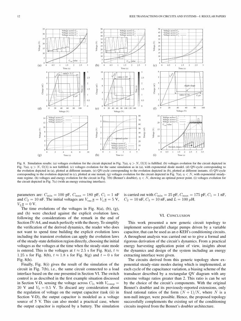
12 IEEE TRANSACTIONS ON CIRCUITS AND SYSTEMS—I: REGULAR PAPERS
Fig. 8. Simulation results: (a) voltages evolution for the circuit depicted in Fig. 7(a), η > N , Ω(3) is fulfilled. (b) voltages evolution for the circuit depicted inFig. 7(a), η > N , Ω(3) is not fulfilled. (c) voltages evolution for the same simulation as in (a), with exponential diode model. (d) QV-cycle corresponding tothe evolution depicted in (a), plotted at different instants. (e) QV-cycle corresponding to the evolution depicted in (b), plotted at different instants. (f) QV-cyclecorresponding to the evolution depicted in (c), plotted at one instant. (g) voltages evolution for the circuit depicted in Fig. 7(a), η < N , with exponential steady-state regime. (h) voltages and energy evolution for the circuit in Fig. 7(b) (Bennet’s doubler), η < N , showing an optimal power point. (i) voltages evolution forthe circuit depicted in Fig. 7(c) (with an energy extracting interface).
parameters are: Cmin = 100 pF, Cmax = 180 pF, C1 = 1 nFand C2 = 10 nF. The initial voltages are Vvar,0 = V1,0 = 5 V,V2,0 = 0 V.
The time evolutions of the voltages in Fig. 8(a), (b), (g),and (h) were checked against the explicit evolution laws,following the considerations of the remark in the end ofSection IV-A4, and match perfectly with the theory. To simplifythe verification of the derived dynamics, the reader who doesnot want to spend time building the explicit evolution lawsincluding the transient evolution can apply the evolution lawsof the steady-state definition region directly, choosing the initialvoltages as the voltages at the time when the steady-state modeis entered. This is the voltages at t ≈ 2.5 s for Fig. 8(a), t ≈1.25 s for Fig. 8(b), t ≈ 1.8 s for Fig. 8(g) and t = 0 s forFig. 8(h).
Finally, Fig. 8(i) gives the result of the simulation of thecircuit in Fig. 7(b), i.e., the same circuit connected to a loadinterface based on the one presented in Section VI. The switchcontrol is as described in the first example situation discussedin Section V-D, sensing the voltage across C3, with Vcomp =20 V and Vh = 0.5 V. To discard any consideration aboutthe regulation of voltage on the output capacitor (task (ii) inSection V-D), the output capacitor is modeled as a voltagesource of 5 V. This can also model a practical case, wherethe output capacitor is replaced by a battery. The simulation
is carried out with Cmin = 25 pF, Cmax = 175 pF, C1 = 1 nF,C2 = 10 nF, C3 = 10 nF, and L = 100 μH.
VI. CONCLUSION
This work presented a new generic circuit topology toimplement series-parallel charge pumps driven by a variablecapacitor, that can be used as an e-KEH’s conditioning circuits.A throughout analysis was carried out so to give a formal andrigorous derivation of the circuit’s dynamics. From a practicalenergy harvesting application point of view, insights aboutthe dynamics and design of the system including an energyextracting interface were given.
The circuits derived from this generic topology show ex-ponential steady-state modes during which is implemented, ateach cycle of the capacitance variation, a biasing scheme of thetransducer described by a rectangular QV diagram with anyextreme voltage ratios greater than 2. This ratio is can be setby the choice of the circuit’s components. With the originalBennet’s doubler and its previously-reported extensions, onlyfixed rational ratios of the form (N + 1)/N , where N is anon-null integer, were possible. Hence, the proposed topologysuccessfully complements the existing set of the conditioningcircuits inspired from the Bennet’s doubler architecture.

KARAMI et al.: SERIES-PARALLEL CHARGE PUMP CONDITIONING CIRCUITS FOR ELECTROSTATIC KINETIC ENERGY HARVESTING 13
The non-exponential steady-state mode was also analyzed, inthe case of low capacitance variation value. This analysis alsoholds for the Bennet’s doubler, for which the dynamics of thismode were not described so far.
An example for which the reported topology is advantageousover state-of-the art circuits has been given. However, thisexample is limited to an electrical domain study. To be ableto advocate for a particular conditioning aiming for designand optimization, an electromechanical study is required topredict the full e-KEH’s dynamics. Apart from experimentaland numerical simulation methods, applying semi-analyticaltools that were developed (e.g., in [15]) are a mean to assesssuch a study. Applying these tools requires a comprehension ofthe conditioning circuit’s dynamics, as provided by this paper.
APPENDIX
PROOF OF THE LEMMA USED IN SECTION IV
Consider two fixed capacitors of the network, C1 and C2. Let
Qji ={n ∈ N | n � i, Vvar,n = Vj,n}
Sji =
{n ∈ N | n� i, (Vvar,n−1 = Vj,n−1)∧(Vvar,n �= Vj,n)
}.
(a) Consider a cycle n1 such that Q1n1
∪ Q2n1
= ∅. In thiscase, the evolution laws derived in Section III lead to (evolutionwith no parallel configuration of C1 and/or C2 with Cvar). Asat each cycle, the switching in series will necessarily occur,since η > N
∀n � n1,
V1,n = V1,n1+ 1
C1
n∑k=n1
ΔQk
V2,n = V2,n1+ 1
C2
n∑k=n1
ΔQk
(69)
with ΔQk defined in (13). Thus
∀n � n1, Δn =V1,n − V2,n
=V1,n1− V2,n1
+C2 − C1
C1C2
n∑k=n1
ΔQk (70)
where
n∑k=n1
ΔQk =
n∑k=n1
⎛⎝ Cmin
1 + Cmin
∑Ni=1 Ci
−1
×
⎛⎝Vvar,k(η − pk)−
N∑i=pk+1
Vi,k
⎞⎠⎞⎠ (71)
and where pk is the number of capacitors in parallel with Cvar
in cycle k at Cvar = Cmax. Hence, since for any (k, i) ∈ N×[[1;N ]], Vi,k � Vvar,k, and under the condition η > N
Cmin
1 + Cmin
∑Ni=1 Ci
−1
(Vvar,k(η − pk)−
N∑i=ki+1
Vi,k
)
� CminVvar,n1
(η −N)
1 + Cmin
∑Ni=1 Ci
−1> 0. (72)
Therefore, the sequence (Δn)n�n1diverges to +∞ if and only
if C1 < C2, to −∞ if and only if C2 < C1. Consequently,eventually swapping the capacitors indexes in the case C1 = C2
so as to have V1,n1� V2,n1
∃n′1 � n1, ∀n, n � n′
1 ⇒ (V1,n � V2,n ⇔ C1 � C2). (73)
(b) Consider a cycle n2(i) such that Q1n2(i)
∪ Q2n2(i)
�= ∅.Suppose V1,n2(i)
� V2,n2(i).
(b.1) First, the case whenC1 � C2 is investigated. From (69),with n1 = n2(i), it follows that Q1
n2(i)�= ∅ and:
C1�C2⇒(∀n ∈ [[n2(i);minQ1
n2(i)[[, V1,n � V2,n
).
(74)
(b.1.1) If S1n2(i)
= ∅, (74) can be extended to any cycleafter n2(i)
C1 � C2 ⇒ (∀n, n � n2(i) ⇒ V1,n � V2,n) . (75)
(b.1.2) Now, suppose S1n2(i)
�= ∅.(b.1.2.1) On the one hand, note that
∀n ∈ [[minQ1n2(i)
; minS1n2(i)
[[, V1,n � V2,n. (76)
(b.1.2.2) On the other hand, [see condition (17)]
∀n ∈ Sn2(i), V1,n < Vvar,n (77)
with, from (12), and with ΔQn defined in (13)
∀n, V1,n =V1,n−1 +ΔQn−1
C1
∀n, V2,n =V2,n−1 +ΔQn−1
C2.
(78)
Hence((C1 � C2) ∧
(∀ k ∈ Sn2(i), V1,k−1 � V2,k−1
))⇒ ∀n ∈ Sn2(i), V2,n � V1,n < Vvar,n
⇒ ∀n ∈ Sn2(i), V2,n = V2,n � V1,n = V1,n. (79)
Putting it all together, from (74) and (75) comes
C1�C2⇒(∀n ∈ [[n2(i);minS1
n2(i)[[, V1,n � V2,n
)(80)
and from (79), the above reasoning starting from (b.1) canthen be inductively repeated choosing n2(i+ 1) = minS1
n2(i):
if Q1n2(i)
∪ Q2n2(i)
is not a finite set, then inductively
C1 � C2 ⇒ (∀n, n � n2 ⇒ V1,n � V2,n). (81)
Otherwise, if there exists n2(j) ∈ S1n2(j−1) such that Q1
n2(j)∪
Q2n2(j)
= ∅, then (a) can be applied, choosing n1 = n2(j), andthe same conclusion, i.e., (81), holds.
(b.2) Consider now C2 < C1. Let T a,bi be the set such that:
T a,bi = {n ∈ N | (Va,n � Vb,n) ∧ (n � i)} .

14 IEEE TRANSACTIONS ON CIRCUITS AND SYSTEMS—I: REGULAR PAPERS
Suppose T 2,1n2(i)
= ∅. Then, the laws of variation of voltageson both capacitors are
∀n � n2(i),
V1,n =V1,n2(i)+ 1
C1
n∑k=n2(i)
ΔQk−ΔVn
V2,n=V2,n2(i)+ 1
C2
n∑k=n2(i)
ΔQk
(82)
where the term ΔVn represents decrease of the voltage acrossC1 when it is in parallel with Cvar. As, ∀n, ΔVn � 0, it comes,with (Δn) defined in (70)
V1,n − V2,n � Δn (83)
and as C2 < C1 implies that (Δn)n�n2(i) diverges to −∞,(V1,n − V2,n)n�n2(i) diverges to −∞, and hence a contradic-tion since it would therefore exist n � n2(i) such that V1,n �V2,n. Thus, T 2,1
n2(i)�= ∅ and, applying (b.1) with initial cycle
n2(j) = min T 2,1n2(i)
and swapping the capacitors indexes, allthe cases are covered. Applying the proof to every couple offixed capacitors in the network, the implication part of the proofis concluded for the voltages at Cvar = Cmax. From (12) andthe capacitance values order, it is clear that the conclusion alsoholds for Cvar = Cmin.
The proof of the converse, which is not useful in the applica-tion of the lemma, easily follows by reductio ad absurdum.
REFERENCES
[1] B. C. Yen and J. H. Lang, “A variable-capacitance vibration-to-electricenergy harvester,” IEEE Trans. Circuits Syst. I, Reg. Papers, vol. 53,no. 2, pp. 288–295, 2006.
[2] A. Kempitiya, D.-A. Borca-Tasciuc, and M. M. Hella, “Analysis and op-timization of asynchronously controlled electrostatic energy harvesters,”IEEE Trans. Ind. Electron., vol. 59, no. 1, pp. 456–463, 2012.
[3] S. Roundy, P. K. Wright, and J. Rabaey, “A study of low level vibrationsas a power source for wireless sensor nodes,” Comput. Commun., vol. 26,no. 11, pp. 1131–1144, 2003.
[4] D. Galayko, A. Dudka, A. Karami, E. O’Riordan, E. Blokhina, O. Feely,and P. Basset, “Capacitive energy conversion with circuits implement-ing a rectangular charge-voltage cycle—Part 1: Analysis of the electri-cal domain,” IEEE Trans. Circuits Syst. I, Reg. Papers, vol. 62, no. 9,pp. 2652–2663, 2015.
[5] S. Meninger, J. O. Mur-Miranda, R. Amirtharajah, A. P. Chandrakasan,and J. H. Lang, “Vibration-to-electric energy conversion,” IEEE Trans.Very Large Scale Integr (VLSI) Syst., vol. 9, no. 1, pp. 64–76, 2001.
[6] P. Mitcheson, T. Sterken, C. He, M. Kiziroglou, E. Yeatman, andR. Puers, “Electrostatic microgenerators,” Meas. Control, vol. 41, no. 4,pp. 114–119, 2008.
[7] A. C. M. de Queiroz and M. Domingues, “The doubler of electricity usedas battery charger,” IEEE Trans. Circuits Syst. II, Exp. Briefs, vol. 58,no. 12, pp. 797–801, 2011.
[8] A. Bennet and R. Kaye, “An account of a doubler of electricity,” Philos.Trans. Roy. Soc. London, vol. 77, pp. 288–296, 1787.
[9] E. Lefeuvre, S. Risquez, J. Wei, M. Woytasik, and F. Parrain, “Self-biased inductor-less interface circuit for electret-free electrostatic energyharvesters,” in J. Phys., Conf. Series, vol. 557, 2014, p. 012052.
[10] J. Wei, S. Risquez, H. Mathias, E. Lefeuvre, and F. Costa, “Simple andefficient interface circuit for vibration electrostatic energy harvesters,” inProc. IEEE SENSORS, 2015, pp. 1–4.
[11] A. C. M. De Queiroz, “Electrostatic vibrational energy harvesting usinga variation of Bennet’s doubler,” in Proc. 53rd IEEE Int. Midwest Symp.Circuits Syst, 2010, pp. 404–407.
[12] T. Sterken, P. Fiorini, K. Baert, R. Puers, and G. Borghs, “Anelectret-based electrostatic μ-generator,” in Proc. 12th Int. Conf.TRANSDUCERS, Solid-State Sensors, Actuators, Microsyst., vol. 2, 2003,pp. 1291–1294.
[13] Y. Suzuki, “Electret based vibration energy harvester for sensor network,”in Proc. 18th Int. Conf. Solid-State Sensors, Actuators, Microsystems(TRANSDUCERS), 2015, pp. 43–46.
[14] A. Karami, P. Basset, and D. Galayko, “Electrostatic vibration energy har-vester using an electret-charged mems transducer with an unstable auto-synchronous conditioning circuit,” J. Phys., Conf. Series, vol. 660, no. 1,p. 012025, 2015.
[15] E. O’Riordan, A. Dudka, D. Galayko, P. Basset, O. Feely, andE. Blokhina, “Capacitive energy conversion with circuits implementing arectangular charge-voltage cycle part 2: Electromechanical and nonlinearanalysis,” IEEE Trans. Circuits Syst. I, Reg. Papers, vol. 62, no. 11,pp. 2664–2673, 2015.
Armine Karami (S’14) was born in Paris, France,in 1991. He received the M.S. degree in electricalengineering from Université Pierre et Marie Curie—Paris 6, France, (UPMC) in 2014. He is currentlyworking toward the Ph.D. degree in Université Pierreet Marie Curie (UPMC)—Paris 6, at the Laboratoired’Informatique de Paris 6 (LIP6). His Ph.D. researchis focused on the theory and analysis of electrostatickinetic energy harvesting systems.
Dimitri Galayko (M’12) graduated from OdessaState Polytechnich University, Ukraine, in 1998, hereceived his M.S. degree from Institut of AppliedSciences of Lyon (INSA-LYON), France, in 1999.He made his Ph.D. thesis in the Institute of Mi-croelectronics and Nanotechnologies (IEMN, Lille,France) and received the Ph.D. degree from theUniversity Lille-I in 2002. The topic of hisPh.D. dissertation was the design of microelectro-mechanical silicon filters and resonators for radio-communications. Since 2005 he is an Associate
Professor in University Paris-VI (Pierre et Marie Curie), France, in the LIP6laboratory. His research interests include study, modeling and design of nonlin-ear integrated circuits for sensor interface and for mixed-signal applications.
Philippe Basset received the engineering diplomain electronics from ISEN Lille, France, in 1997 andthe M.Sc. and Ph.D. degrees from IEMN Universityof Lille in 1999 and 2003, respectively. In 2004he was a Postdoc at Carnegie Mellon University,Pittsburgh, PA, USA. In 2005 he joined ESIEE Parisat the Université Paris-Est, France, where he is cur-rently an Associate Professor. His research interestsinclude micro/nanostructuration of silicon and mi-cropower sources for autonomous MEMS. He ledseveral projects on energy harvesting using micro-
and nanotechnologies and he serves in the TPC of the PowerMEMS conferencesince 2013. Member of the ESYCOM laboratory, he is currently leading theSensors and Measuring MEMS group.