sensoray model 7421 stdbus analog/digital i/o · pdf filesensoray model 7421 stdbus...
TRANSCRIPT

Sensoray Co. Inc.7313 SW Tech Center Drive
Tigard, OR 97223503-684-8005 Phone 503-684-8164 Fax
[email protected] www.sensoray.com
Sensoray Model 7421STDbus Analog/Digital I/O Card
Rev F — 07/28/1999

Table of Contents
Limited Warranty 1
Special Handling Instructions 1
Introduction 2
Block Diagram 2
Selecting a Base Address 3
Fault Indicator 3
Status Register 3
Reset 4
Watchdog Timer 4
Encoder Interface 5
Relay Interface 8
D/A Interface 9
A/D Interface 12
Appendix A: Specifications 15
Appendix B: I/O Map Summary 16
Appendix C: Configuration Jumpers 17
Appendix D: Connector Pinouts 18
Appendix E: Programming 19
Schematics 25

Sensoray Model 7421 Instruction Manual Page 1
Limited Warranty
Sensoray Company, Incorporated (Sensoray) warrants the Model 7421 hardware to be free from defects in material and workmanship and perform to applicable published Sensoray specifications for one year from the date of shipment to purchaser. Sensoray will, at its option, repair or replace equipment that proves to be defective during the warranty period. This warranty includes parts and labor.
The warranty provided herein does not cover equipment subjected to abuse, misuse, accident, alteration, neglect, or unauthorized repair or installation. Sensoray shall have the right of final determination as to the existance and cause of defect.
As for items repaired or replaced under warranty, the warranty shall continue in effect for the remainder of the original warranty period, or for ninety days following date of shipment by Sensoray of the repaired or replaced part, whichever period is longer.
A Return Material Authorization (RMA) number must be obtained from the factory and clearly marked on the outside of the package before any equipment will be accepted for warranty work. Sensoray will pay the shipping costs of returning to the owner parts which are covered by warranty.
Sensoray believes that the information in this manual is accurate. The document has been carefully reviewed for technical accuracy. In the event that technical or typographical errors exist, Sensoray reserves the right to make changes to subsequent editions of this document without prior notice to holders of this edition. The reader should consult Sensoray if errors are suspected. In no event shall Sensoray be liable for any damages arising out of or related to this document or the information contained in it.
EXCEPT AS SPECIFIED HEREIN, SENSORAY MAKES NO WARRANTIES, EXPRESS OR IMPLIED, AND SPECIFICALLY DISCLAIMS ANY WARRANTY OF MERCHANTABILITY OR FITNESS FOR A PARTICULAR PURPOSE. CUSTOMER’S RIGHT TO RECOVER DAMAGES CAUSED BY FAULT OR NEGLIGENCE ON THE PART OF SENSORAY SHALL BE LIMITED TO THE AMOUNT THERETOFORE PAID BY THE CUSTOMER. SENSORAY WILL NOT BE LIABLE FOR DAMAGES RESULTING FROM LOSS OF DATA, PROFITS, USE OF PRODUCTS, OR INCIDENTAL OR CONSEQUENTIAL DAMAGES, EVEN IF ADVISED OF THE POSSIBILITY THEROF.
Special Handling Instructions
The Model 7421 circuit board contains CMOS circuitry that is sensitive to Electrostatic Discharge (ESD). Special care should be taken in handling, transporting, and installing the 7421 to prevent ESD damage to the board. In particular:
— Do not remove the 7421 from its protective antistatic bag until you are ready to configure the board for installation.
— Handle the 7421 only at grounded, ESD protected stations.
— Remove power from the STDbus before installing or removing the 7421 circuit board.

Page 2 Sensoray Model 7421 Instruction Manual
Introduction
Block Diagram
Power for linear circuitry is derived from an on-board DC-to-DC converter. Wherever possible, low power CMOS circuitry is used to minimize system power consumption and enhance reliability.
The board occupies a 16-byte block of I/O addresses in the STDbus 8-bit I/O space. Programming shunts may be installed to map the board to any 16-byte address boundary.
Three headers are provided for connecting on-board peripherals to external circuitry. Right-angle headers are used to satisfy the tight clearances mandated by modern high-density system designs. All headers are supplied with latches to ensure reliable operation in vibrating environments.
The Sensoray model 7421 is an STDbus I/O card that performs several functions commonly required in embedded applications. On-board peripherals include:
— Programmable watchdog timer.
— 24 digital I/O channels.
— 12-bit analog-to-digital converter with eight differential input channels and resistor-programmed gain.
— Four 12-bit analog output channels.
— Three 16-bit counter channels optimized for interface to incremental encoders.
The 7421 is powered from the STDbus 5-volt supply. No auxilliary 12- or 15-volt supplies are required.
8-channelDiff Mux
LO
CA
L B
US
ST
D B
US
Digital I/OInterface
3 x 16-bitCounters
SignalConditioning
System BusDecode
SystemData BusBuffer
12-bit D/A
12-bit D/A
12-bit D/A
12-bit D/A
12-bit A/D
InstrumentAmplifier
WatchdogTimer
DC-to-DCConverter
Analog I/OConnector
Digital I/OConnector
EncoderConnector

Sensoray Model 7421 Instruction Manual Page 3
Selecting a Base Address.
BoardAddressRange
Jumper Settings
A4 A3 A2 A1
00 to 0F Install Install Install Install
10 to 1F Install Install Install Remove
20 to 2F Install Install Remove Install
30 to 3F Install Install Remove Remove
40 to 4F Install Remove Install Install
50 to 5F Install Remove Install Remove
60 to 6F Install Remove Remove Install
70 to 7F Install Remove Remove Remove
80 to 8F Remove Install Install Install
90 to 9F Remove Install Install Remove
A0 to AF Remove Install Remove Install
B0 to BF Remove Install Remove Remove
C0 to CF Remove Remove Install Install
D0 to DF Remove Remove Install Remove
E0 to EF Remove Remove Remove Install
F0 to FF Remove Remove Remove Remove
Fault IndicatorStatus Register
A status register, located at the board base address + 11, makes available four status bits for access by the STDbus host processor. The status register is organized as follows:
STATUS (11):
Status bits are all active high and have the following definitions:
WD — indicates watchdog timer timed out.
UN — indicates A/D converter is programmed for unipolar operation.
BZ — indicates that the A/D converter is busy digitizing an analog input.
DE — indicates that all four DAC output channels have been enabled via the CHCTRL port.
PD — indicates 7421 is in the low-power standby mode, controlled by the RELAY2 port.
x x x WD UN DE BZ FT
A red light-emitting diode located near the upper-left corner of the circuit board indicates reset and fault conditions.
In normal operation, the indicator is turned on only during system or 7421 local reset. The indicator should be off at all other times.
If the fault indicator remains on for more than one second following a reset, a fault condition may exist on the board that requires servicing.
Before servicing the unit, make sure that your STDbus host CPU is not invoking repeated soft resets of the 7421 (which will also keep the indicator turned on).
The 7421 board occupies a block of 16 consecutive addresses in the STDbus 8-bit I/O space. The address range occupied by the board must begin on a 16-byte address boundary. The first address in the block — the “base address” — is assigned by installing configuration option jumpers A1 through A4.
Care must be exercised to ensure that no other devices use addresses in the address range assigned to the 7421. Use the table shown at the right to determine the proper address jumper settings for your application.
Option jumper EXP selects the active state of the STDbus IOEXP signal. This jumper should be installed to select IOEXP active low, or removed to select IOEXP active high.
Many STDbus CPU boards implement a 16-bit I/O address space. These boards typically map a block of 256 addresses as a “window” into the 8-bit I/O space. If you are using this type of CPU, refer to the manufacturer’s literature for information on addressing 8-bit I/O cards.

Page 4 Sensoray Model 7421 Instruction Manual
Reset
Watchdog Timer
The 7421 may be reset by either a “hard reset” from the STDbus system reset signal or a “soft reset” under software control of the STDbus master.
Soft Reset
A “soft reset” may be performed at any time. This causes a local reset on only the 7421 and will not reset any other devices on the STDbus. A soft reset is invoked by writing to the RESET port.
RESET (11): x x x x x x x x
The value written to the RESET port is ignored.
Default State Following a Reset
Both hard and soft resets force the 7421 to its default power-up state:
— All relay channels are turned off.
— The watchdog timer is disabled.
— All DAC outputs are disabled.
— All encoder counters are reset to zero.
CHCTRL (12):
Set W to logic one to enable the watchdog or zero to disable the watchdog. Note that D is used to enable and disable DAC outputs. Make sure D is set properly when changing the watchdog enable bit so that you don’t inadvertently enable or disable the DAC outputs.
Refreshing the Watchdog
The watchdog is refreshed by writing to the HITDOG port. The data value written to this port is ignored by the 7421.
HITDOG (15):
Routing the Watchdog to the STDbus
A watchdog timeout may be programmed to generate either a system reset (via STDbus “pushbutton reset”) or non-maskable interrupt (NMI). Two option jumpers are provided to configure the appropriate signal routing: install option jumper NMIRQ to generate NMI, or install PBRST to generate a pushbutton reset. You may leave both NMIRQ and PBRST uninstalled if you will not be using the watchdog function.
Option Jumper Watchdog Routing
NMIRQ Non-maskable Interrupt
PBRST Pushbutton Reset
0 0 0 0 1 0 D W
x x x x x x x x
Embedded systems often include a watchdog timer to regain program control following an unplanned loss of control by the STDbus master. In such systems, the CPU is responsible for periodically refreshing the watchdog timer to prevent a timeout. Should the CPU crash, the watchdog will not be refreshed and will eventually timeout. The resulting timeout will restart the CPU.
Depending on whether the short or long watchdog timeout interval (WDTI) has been selected, the time between any two watchdog refreshes must not exceed 700 milliseconds or 11 seconds, respectively.
Some CPU’s are not able to refresh the watchdog at the mandatory minimum rate during system boot or critical I/O operations. To accomodate these situations, the 7421 provides a control register for enabling and disabling the watchdog under program control. The first watchdog refresh must occur no later than WDTI after enabling the timer. The watchdog is automatically disabled by a soft reset or system-wide hard reset.
Selecting the Watchdog Timeout Interval
Option shunt WDS is used to select the desired WDTI setting. Install a shunt at WDS (default) to select the 700 millisecond interval, or remove the shunt to select the 11 second interval.
Enabling/Disabling the Watchdog
The watchdog is enabled and disabled by writing to the CHCTRL port at board base address + 12:

Sensoray Model 7421 Instruction Manual Page 5
Encoder Interface
Three quadrature-encoded input channels reside on the 7421. Each channel is optimized for incremental encoders by providing the following elements:
— Input buffers - buffers and conditions encoder signals with input hysterisis for low-slew rates.
— Decode logic - synchronizes encoder signals, then detects and converts encoder edges into clock and direction signals.
— 16-bit up/down counter - maintains encoder position without resorting to multiple counter channels.
— Power - STDbus 5-volts is accessible to power encoder.
In addition to the channel logic, additional logic is incorporated to implement synchronous transfer of encoder counts into a 16-bit holding register. This feature assures seamless acquisition of encoder counts by the STDbus master.
Counter Control
Unlike conventional counters, the 7421 encoder counters do not accumulate errors when the encoder changes direction or dithers about a clock boundary.
Encoder channels count both up and down by decoding the phase relationship of the two encoder signals. Each channel has two quadrature encoded input signals (or “phases”): A and B, 90 degrees out of phase. The counters count up when A leads B, and count down when B leads A.
Count events occur on both the rising and falling edges of the A phase, while B phase is used strictly for direction control. Consequently, encoder counters have twice the resolution of the physical encoder.
For example, one revolution of a 100 pulse/rev encoder will produce a change of 200 counts on the associated encoder counter.
Note: because both edges of the A phase are used for clocking, it is not possible to apply 7421 encoder channels as conventional single-phase counters.
Reset
Hardware or software reset of the 7421 will asynchronously zero all three encoder counters and the 16-bit data holding register. Channel logic is re-enabled for counting upon termination of the reset pulse.
Rollover
All 16-bit encoder counters will increment from FFFF to 0000 when counting up, and will decrement from 0000 to FFFF when counting down. No interrupts or status flags are available to notify the STDbus master of a rollover event. The master should read encoder position data with sufficient frequency to guarantee the validity of position data.
Input Bufferw/Hysterisis
DecodeLogic
Up/DownCounter
DA
TA
SE
LE
CT
OR
Input Bufferw/Hysterisis
DecodeLogic
Up/DownCounter
Input Bufferw/Hysterisis
DecodeLogic
Up/DownCounter
Timing &Control
16-bit DataRegister
EncoderInputsData to
STDbusHost
Encoder Interface Block Diagram

Page 6 Sensoray Model 7421 Instruction Manual
Command Functions
transfers the selected counter contents to the 16-bit data holding register. The Reset command resets the selected counter to zero.
Note: a Latch command must be executed before attempting to read the contents of an encoder counter.
The CNTCTL port is used to invoke all encoder command functions. Two parameters must be specified for each command: encoder channel and operation to be performed. See the box below for details.
Two commands are available for each channel: Latch and Reset. The Latch command synchronously
S1/S0 select encoder channel to be operated on:
S1 S0 Selected Encoder Channel
0 0 Channel 0
0 1 Channel 1
1 0 Channel 2
1 1 Reserved for future use
M specifies the operation to be performed:
M Function
0 Latch counts in holding register
1 Reset counter to zero
CNTCTL (14): x x x x x M S1 S0
Reading Latched Encoder Counts
After executing a Latch command, the latched data may be read from ports CNTLSB and CNTMSB.
CNTLSB (14):
CNTMSB (15):
Port CNTLSB contains the least-significant byte of the encoder counts and port CNTMSB contains the most-significant byte. It makes no difference which byte is read first. The data value remain latched until the next Latch command.
Encoder Connections
Connector P4 is used to make all electrical connections to external encoders. Each counter channel is allocated six pins on connector P4: +5V, GND, +A, -A, +B and -B.
d7 d6 d5 d4 d3 d2 d1 d0
d15 d14 d13 d12 d11 d10 d9 d8
Power Connections
The +5V and GND pins may optionally be used to power an external encoder. If an external encoder power source is used, you must connect GND to the external power supply return. Failure to connect these returns may damage the 7421 board.
Clock Connections
Each counter channel is assigned four pins on connector P4 for connection to the phase inputs. Each phase makes two electrical connections to P4 in the form of a differential RS422 pair. The A phase inputs consist of +A and -A, while the B inputs consist of +B and -B. Connections to these four inputs depend on the type of device to be interfaced.
For a variety of reasons, RS422 termination resistors are not supplied on the 7421 board. If your encoder (or other pulse source) employs RS422 drivers, you may need to supply external termination resistors near connector P4 for proper operation. Refer to your encoder manufacturer’s documentation for recommended RS422 termination circuitry and practice.

Sensoray Model 7421 Instruction Manual Page 7
Connector P4 Pinout:
Pin Name Function1 +5V Channel 0 +5V power2 +A0 Channel 0 phase A input (+)3 GND Channel 0 5V return4 +B0 Channel 0 phase B input (+)5 +5V Channel 1 +5V power6 +A1 Channel 1 phase A input (+)7 GND Channel 1 5V return8 +B1 Channel 1 phase B input (+)9 +5V Channel 2 +5V power
10 +A2 Channel 2 phase A input (+)11 GND Channel 2 5V return12 +B2 Channel 2 phase B input (+)13 -- no connect --14 -- no connect --15 -A0 Channel 0 phase A input (-)16 -A1 Channel 1 phase A input (-)17 -A2 Channel 2 phase A input (-)18 -B0 Channel 0 phase B input (-)19 -B1 Channel 1 phase B input (-)20 -B2 Channel 2 phase B input (-)
Counter channels may be interfaced to devices that produce a single output phase. In such cases, the counters are configured for operation in either mode 3 or mode 7. Connect the device output to the +A input. Connect the +B input to GND. Leave the -A and -B inputs disconnected:
Many encoders utilize single-ended TTL or CMOS compatible outputs. If you are using this type of encoder, connect the encoder A output to the +A input and connect the encoder B output to the +B input. Leave the -A and -B inputs disconnected:
A
B
Encoder +A
-A
+B
-B
+5V
GND
VCC
GND
P3
OUTDevice +A
-A
+B
-B
+5V
GND
VCC
GND
P3
A
B
Encoder +A
-A
+B
-B
+5V
GND
VCC
GND
P3
Some encoders have built-in RS422 drivers. If you are using this type of encoder, connect the encoder A outputs to the +A and -A inputs, and connect the encoder B outputs to the +B and -B inputs:

Page 8 Sensoray Model 7421 Instruction Manual
Relay Interface
Register
I/O Channel
LocalDataBus
One of 24 Digital I/O Channels
RELAYx Ports
The 24 digital I/O channels are organized as a bank of three byte wide ports. Each port accesses eight relay channels simultaneously.
RELAY0 ( 8):
RELAY1 ( 9):
RELAY2 (10):
Each RELAYx port may be read from or written to at any time. Reading from a RELAYx port returns the physical state of the channels associated with that port. Writing to a RELAYx port programs the associated relay channel output registers.
Note: the value read from a relay channel may not be the same as the value stored in that channels output register. Specifically, the values will differ if an output register is programmed to 0 and an external sink pulls the corresponding channel down to 0V.
Configuring I/O Type
Each channel may be independently configured as either an input or output via software. To configure a channel as an input, set the associated channel register to 0.
Connections
All electrical connections are made through 50-pin header connector P3. One pin is assigned to each active-low I/O channel. All even pins are connected to STDbus five volt return. In addition, pin 49 may be used to supply limited five volt power (<100mA) to an external relay rack.
r7 r6 r5 r4 r3 r2 r1 r0
r15 r14 r13 r12 r11 r10 r9 r8
r23 r22 r21 r20 r19 r18 r17 r16
The 7421 provides 24 high-current digital I/O channels for direct interface to an industry standard relay rack.
As shown in the diagram to the right, digital I/O channels are physically structured as open-collector buffers (with pullup resistors) looped back to the local data bus by tri-state buffers.
Channel data is active high on the local bus side, and active low on the I/O channel side.
Connector P3: Digital I/O
Pin Name Function1 CH0 I/O Channel 03 CH1 I/O Channel 15 CH2 I/O Channel 27 CH3 I/O Channel 39 CH4 I/O Channel 411 CH5 I/O Channel 513 CH6 I/O Channel 615 CH7 I/O Channel 717 CH8 I/O Channel 819 CH9 I/O Channel 921 CH10 I/O Channel 1023 CH11 I/O Channel 1125 CH12 I/O Channel 1227 CH13 I/O Channel 1329 CH14 I/O Channel 1431 CH15 I/O Channel 1533 CH16 I/O Channel 1635 CH17 I/O Channel 1737 CH18 I/O Channel 1839 CH19 I/O Channel 1941 CH20 I/O Channel 2043 CH21 I/O Channel 2145 CH22 I/O Channel 2247 CH23 I/O Channel 2349 +5V +5V powerEven GND 5V return

Sensoray Model 7421 Instruction Manual Page 9
D/A Interface
.
DACDAC0LSB8-bit Register
DAC0MSB4-bit Register
12-bitOutputRegister
DAC EnableRegister
CMOSSwitch
E
0 to +10VOutput
LocalDataBus
G
DAC Channel 0(1 of 4 channels shown)
LDAC EG DAC
Channel 1
EG DAC
Channel 2
EG DAC
Channel 3
D/A Subsystem Block Diagram
(DACEN)
DAC Enable Register
Each DAC channel consists of a low-byte/high-nibble bus register pair, 12-bit output register, 12-bit D/A converter, and CMOS switch.
All four CMOS switches are enabled by the one-bit DAC Enable Register. When enabled, the CMOS switches connect all four DAC outputs to 40-pin
header P2. When disabled, all DAC output signals at P2 are pulled down to zero volts.
A control strobe — LDAC — simultaneously transfers data from the four bus register pairs to their corresponding 12-bit output registers. DAC output ranges are fixed at 0 to +10 volts.
Following a reset, the four 12-bit DAC output registers contain indeterminate values. To ensure orderly startup, the DAC Enable Register (DACEN) turns off all CMOS switches to prevent random DAC voltages from reaching the analog I/O connector.
DACEN — which is automatically cleared by a reset — may be manipulated by the STDbus master. The DACEN register is accessed through the write-only CHCTRL port.
CHCTRL (12):
The D bit enables DAC outputs when set to 1 and disables DAC outputs when set to 0.
Note: the W bit, which enables and disables the watchdog timer, is also controlled by this port. Make sure you don’t inadvertently change the watchdog enable bit when enabling or disabling the DAC outputs.
0 0 0 0 1 0 D W

Page 10 Sensoray Model 7421 Instruction Manual
DAC Data Ports
Each DAC is allocated two output ports —DACxLSB and DACxMSB (where x is the DAC identifier 0, 1, 2, or 3) — called bus registers. All DAC setpoint data are written into these registers.
DACxLSB is the D/A converter least-significant data byte register, and DACxMSB is the most-significant data nibble register. The data value is right-justified in the DACxMSB registers.
Data may be written to the DACxLSB or DACxMSB registers in any order.
Note: DAC outputs do not change when the DACxLSB and DACxMSB registers are written to. DAC outputs change only when the LDAC port is read (see next section).
.
Base AddressOffset
Function
0 DAC0LSB
1 DAC0MSB
2 DAC1LSB
3 DAC1MSB
4 DAC2LSB
5 DAC2MSB
6 DAC3LSB
7 DAC3MSB
LDAC Port
DAC outputs change when data is transferred from the bus registers into the corresponding DAC output registers.
The LDAC port is used to transfer data from bus registers to output registers. Reading from the LDAC port transfers data to all four DAC output registers simultaneously.
LDAC (0):
The data value returned from the LDAC port is indeterminate and has no meaning.
x x x x x x x x
DAC Initialization
Before setting the DAC Enable Register to enable DAC outputs, the STDbus master should first zero all DAC output registers. Execute this event sequence to achieve orderly startup following a reset:
— Write zeros to all DACxLSB and DACxMSB registers.
— Read from the LDAC port to change all DAC outputs to 0 volts.
— Enable DAC outputs by setting the CHCTRL port D bit.
Transfer Function
The relationship between DAC input code and output voltage is shown in the following table. Input coding for DAC channels is unsigned binary.:
Data Value (hexadecimal)
Output Level(volts)
000 0.0000
001 0.0024
7FF 4.9976
800 5.0000
801 5.0024
FFF 9.9976
Channel Differences
DAC channel 0 is identical to the other channels except for the addition of a remote sense function.
Each channel has an output source impedance specified at 85 ohms, maximum. Because channel 0 senses the DAC output after its CMOS switch, however, its effective source impedance is zero for output currents up to the specified maximum.
Because of their 85 ohm source impedances, channels 1, 2, and 3 will tend to exhibit “gain error” as a function of load current. This is not a problem as long as the load current is constant, and hence, DAC output voltage is monotonic.
Use DAC channel 0 if load impedance varies significantly or absolute accuracy is important for your application. Alternately, any of the channel 1, 2, or 3 outputs may be buffered by external amplifiers.

Sensoray Model 7421 Instruction Manual Page 11
Connections: Channel 1, 2, and 3
Each DAC channel makes two connections to the 7421: 0 to +10V output, and output return.
Connector Pinout
All external circuitry connects to the DAC channels through 40-pin header P2. Connector P2 is shared by the D/A and A/D converter circuits.
The table below defines that portion of connector P2 used for the DAC channels.
Pin on Conn P2 Function
1 Channel 0 output
19 Channel 0 sense
3 Channel 0 return
5 Channel 1 output
7 Channel 1 return
9 Channel 2 output
11 Channel 2 return
13 Channel 3 output
15 Channel 3 return
0-10V Out
Return
Load
Connections: Channel 0
In addition to output and return, channel 0 has a connection for remote voltage sensing. The remote sense signal must be connected to the output signal. Connect the output and sense signals near to the load for best accuracy.
0-10V Out
Return
Remote Sense Load
Connections: Channel 0 with External Buffer
In applications that use an external buffer for DAC channel 0, it is best to sense the voltage at the buffer output instead of the DAC output.
0-10V Out
Return
Remote Sense Load
V+

Page 12 Sensoray Model 7421 Instruction Manual
A/D Interface
Starting a Conversion
A/D conversions are started by writing to the ADSTART port. The data value written to this port is ignored.
ADSTART (13):
Writing to this port starts a conversion and sets the BZ flag (A/D busy flag) in the status register. When the conversion ends, approximately 9 microseconds after start of conversion, the BZ flag is reset to zero and the binary result may be accessed.
x x x x x x x x
Selecting an Input Channel
Analog input channels are selected by writing the desired channel number to the CHCTRL port. Valid channel numbers range from 0 to 7, inclusive.
CHCTRL (12):
Channel numbers may be written to CHCTRL at any time, but in general should not be done during an A/D conversion.
Sufficient settling time must be allowed between writing a new value to CHCTRL and starting a conversion. 90 microseconds settling time is adequate for low impedance analog sources. If you are digitizing high impedance sensors or using high gain ratios, longer settling delays may be required to meet specified performance.
0 0 0 0 0 N2 N1 N0
Reading the Conversion Result
Binary A/D conversion results may be read from ports ADLSB and ADMSB. Port ADLSB contains the least-significant data byte. Port ADMSB contains the most-significant nibble, right justified with leading zeros.
ADLSB (12):
ADMSB (13):
Data from port ADLSB must be read first, followed by data from ADMSB. These I/O ports must be read once and only once at the end of each A/D conversion. A minimum delay of 1.5µs is required
d7 d6 d5 d4 d3 d2 d1 d0
0 0 0 0 d11 d10 d9 d8
The 7421 digitizer section consists of an eight-input differential CMOS analog multiplexer, resistor programmed instrumentation amplifier, and high speed 12-bit analog-to-digital converter.
A/D conversions are accomplished by executing the following event sequence:
— Select analog input channel to be digitized.
— Start an A/D conversion.
— Wait for conversion to finish.
— Read conversion result.
Each of these steps are discussed in detail below.
Configuring Unipolar/Bipolar Operation
All analog input channels may be collectively programmed for either unipolar or bipolar operation. Option jumper “UNI” is used to configure the operating mode.
Install a shunt at UNI to configure all channels for unipolar operation. Remove the shunt from UNI to configure all channels for bipolar operation.
UNI Mode
Installed Unipolar
Removed Bipolar
Data Format
A/D output data format is a function of the digitizer operating mode.
In the unipolar mode, output data is formatted as 12-bit unsigned binary integers with leading zeros in the most-significant nibble.
In the bipolar mode, output data is formatted as 12-bit signed (two’s complement) integers with leading zeros in the most-significant nibble.

Sensoray Model 7421 Instruction Manual Page 13
Gain Trim
Since it is unlikely that the gain setting resistor R3 will produce the exact gain value desired, a gain trim adjustment is provided on the 7421
A/D front-end gain may be trimmed by adjusting potentiometer R2. The trimmer provides an adjustment range of approximately plus and minus seven percent.
Gain Programming
A/D front-end gain may be set to any desired value greater than or equal to unity via selection of a gain programming resistor. Note that all analog input channels have the same gain. Changing the front-end gain affects all channels. As shipped from the factory, the front-end gain is set to unity.
The front-end gain may be programmed by installing a resistor at position R3. For any arbitrary gain R3 can be calculated using the formula
Note that for Gain = 1, R3 must be an open circuit (default as shipped from the factory).
To minimize gain drift, R3 should have a low temperature coefficient — 50 ppm/C or better for the best performance.
The table below shows required values of R3 for various gains using standard 1% resistor values. The listed gain values are nominal and may be trimmed to exact values as described in the next section.
R3(ohms)
Gain Input RangeUnipolar Bipolar
Open 1 0 to +10V -5 to +5V49.9K 2 0 to +5V -2.5 to +2.5V12.4K 5 0 to +2V -1V to +1V5.49K 10 0 to +1V -500 to +500mV2.61K 20 0 to +500mV -250 to +250mV1.00K 50 0 to +200mV -100 to +100mV499 100 0 to +100mV -50 to +50mV249 200 0 to +50mV -25 to +25mV100 500 0 to +20mV -10 to +10mV49.9 1000 0 to +10mV -5 to +5mV
R3 49400
Gain 1–-------------------=
Unipolar-mode Transfer Function
As discussed earlier, A/D output codes are represented as 12-bit unsigned integers in the unipolar mode. Output values range from 0 at zero volts input to 4095 at the positive full-scale input voltage.
The following table shows the relationship between input voltage and A/D output codes. A 0 to +10 volt gain range (unity gain) is assumed for this illustration.
Input Voltage Output Code
0.000V 000
2.441mV 001
4.998V 7FF
5.000V 800
5.002V 801
+9.997V FFF
Bipolar-mode Transfer Function
A/D output codes are formatted as 12-bit signed two’s complement integers in the bipolar mode. Output values range from -2048 at negative full-scale input to +2047 at positive full-scale input voltage.
The following table shows the relationship between input voltage and A/D output codes. A -5 to +5 volt gain range (unity gain) is assumed for this illustration.
Input Voltage Output Code
-5.000V 800
-4.997V 801
-2.441mV FFF
0.000V 000
+2.441mV 001
+4.997V 7FF

Page 14 Sensoray Model 7421 Instruction Manual
Connector Pinout
All differential analog inputs connect to 40-pin header connector P2. This connector is shared by 7421 analog input and analog output functions. The table below describes that portion of P2 related to analog input functions. Note that the GND signals are related to both analog input and output functions.
Connector P2: Analog I/O
Pin Name Function2 ADC0+ A/D channel 0 positive input4 ADC0- A/D channel 0 negative input6 ADC1+ A/D channel 1 positive input8 ADC1- A/D channel 1 negative input10 ADC2+ A/D channel 2 positive input12 ADC2- A/D channel 2 negative input14 ADC3+ A/D channel 3 positive input16 ADC3- A/D channel 3 negative input18 ADC4+ A/D channel 4 positive input20 ADC4- A/D channel 4 negative input22 ADC5+ A/D channel 5 positive input24 ADC5- A/D channel 5 negative input26 ADC6+ A/D channel 6 positive input28 ADC6- A/D channel 6 negative input30 ADC7+ A/D channel 7 positive input32 ADC7- A/D channel 7 negative input33 GND Analog common34 GND Analog common38 GND Analog common39 GND Analog common40 GND Analog common
Input Connections
Each analog input channel makes two connections to the 7421 board. These two connections constitute a differential input pair. The digitizer measures the difference in voltage between the two inputs.
Note that the input common-mode voltage — the voltage at either input relative to STDbus five volt return (GND) — should not exceed plus or minus 10 volts. Minor excursions beyond this limit will cause inaccurate measurements. Significant excursions may result in damage to digitizer circuitry. Refer to the 7421 specifications section for further details.
All analog input sources should be referenced to STDbus GND. If you are connecting an isolated source (a source not referenced to GND), you should tie one side of the source to GND. Since analog input channels are true differential, it doesn’t matter which side is connected to GND.

Sensoray Model 7421 Instruction Manual Page 15
Appendix A: Specifications
Bus Interface Type STD-80, I/O slave, 8-bit address, 8-bit data
Address requirements 16-byte block starting on any 16-byte boundary
Watchdog Timer Timeout (short interval) 700 milliseconds. ± 5%.
Timeout (long interval) 11.2 seconds. ± 5%.
Encoder Interface Type Quadrature encoded, single-ended
Input characteristics TTL/CMOS compatible, 10Kohm pullup to +5V
Pulse rate 0 Hz, min. 375 KHz, max.
5V current, per channel 100 mA, max.
Relay Interface Input characteristics TTL/CMOS compatible, 10Kohm pullup to +5V
Output sink current 60 mA, min.
A/D Interface A/D type 12 bits, successive approximation
Settling time (G = 1) 90 microseconds, max.
Conversion time 10 microseconds, max.
CMRR (G = 1) 73 dB min. 90 dB typical
Analog input -25 Volts, absolute min. +25 Volts, absolute max.
Offset error ± 3 LSB, max.
Input impedance 10 megohms, min.
D/A Interface D/A type 12 bits, voltage output, output range fixed at 0 to +10V
Gain error ± 3 LSB, max.
Output offset ± 7.5 millivolts, max.
Output Impedance 85 ohms, max.
Power Operating range +4.75 Volts, min. +5.25 Volts, max.
Quiescent current 200 mA, typical

Page 16 Sensoray Model 7421 Instruction Manual
Appendix B: I/O Map Summary
Adrs Write Function Read Function
0 DAC0LSB Loads DAC 0 LSB register without updating the DAC output.
LDAC Transfers all DACxMSB and DACxLSB data to the DAC output registers, updating all DAC outputs simultaneously. The returned data value has no meaning.1 DAC0MSB
Loads DAC 0 MSB register without updating the DAC output.
2 DAC1LSB Loads DAC 1 LSB register without updating the DAC output.
3 DAC1MSB Loads DAC 1 MSB register without updating the DAC output.
4 DAC2LSB Loads DAC 2 LSB register without updating the DAC output.
5 DAC2MSB Loads DAC 2 MSB register without updating the DAC output.
6 DAC3LSB Loads DAC 3 LSB register without updating the DAC output.
7 DAC3MSB Loads DAC 3 MSB register without updating the DAC output.
8 RELAY0 Sets relay channels 0-7 simultaneously. All bits are active high.
RELAY0 Returns the states of relay channels 0-7. All bits are active high.
9 RELAY1 Sets relay channels 8-15 simultaneously. All bits are active high.
RELAY1 Returns the states of relay channels 8-15. All bits are active high.
A RELAY2 Sets relay channels 16-23 simultaneously. All bits are active high.
RELAY2 Returns the states of relay channels 16-23. All bits are active high.
B RESET Force a local reset on the 7421, returning it to its default power-up state. All relay channels are turned off, and the watchdog timer and DAC outputs are disabled.
STATUS Returns 7421 status. All status bits are active high. Status bits have the following meanings: UN=A/D unipolar mode, DE=DAC chan-nels enabled, BZ=A/D subsystem busy, FT=7421 fault.
C CHCTRL Declare A/D channel or set hardware enables. The “M” bit speci-fies the meaning of N0-N2 bits: 0=set A/D channel, 1=set enables. If M=1, N0 enables watchdog and N1 enables DAC outputs.
ADLSB Returns the least-significant data byte (lsb) from the last A/D con-version. The lsb must be read before the msb to ensure proper operation.
D ADSTART Start an A/D conversion.
ADMSB Returns the most-significant data nibble from the last A/D conver-sion.
E CNTCTL Latch or reset an encoder counter. S0 and S1 select the counter channel: 00=chan0, 01=chan1, 1x=chan2. The “M” bit specifies the operation to be performed: 0=latch, 1=reset.
CNTLSB Returns the least-significant byte from the encoder counter latch register.
F HITDOG Restart the watchdog timer.
CNTMSB Returns the most-significant byte from the encoder counter latch register.
d7 d6 d5 d4 d3 d2 d1 d0 x x x x x x x x
x x x x d11 d10 d9 d8
d7 d6 d5 d4 d3 d2 d1 d0
x x x x d11 d10 d9 d8
d7 d6 d5 d4 d3 d2 d1 d0
x x x x d11 d10 d9 d8
d7 d6 d5 d4 d3 d2 d1 d0
x x x x d11 d10 d9 d8
r7 r6 r5 r4 r3 r2 r1 r0 r7 r6 r5 r4 r3 r2 r1 r0
r15 r14 r13 r12 r11 r10 r9 r8 r15 r14 r13 r12 r11 r10 r9 r8
r23 r22 r21 r20 r19 r18 r17 r16 r23 r22 r21 r20 r19 r18 r17 r16
x x x x x x x x x x x x UN DE BZ FT
x x x x M N2 N1 N0 d7 d6 d5 d4 d3 d2 d1 d0
0 0 0 0 0 0 0 0 0 0 0 0 d11 d10 d9 d8
x x x x x M S1 S0 c7 c6 c5 c4 c3 c2 c1 c0
x x x x x x x x c15 c14 c13 c12 c11 c10 c9 c8

Sensoray Model 7421 Instruction Manual Page 17
Appendix C: Configuration Jumpers
EXP IOEXP
Install Active Low
Remove Active High
Option Jumper Watchdog Routing
NMIRQ Non-maskable Interrupt
PBRST Pushbutton ResetUNI Mode
Installed Unipolar
Removed Bipolar
BoardAddressRange
Jumper Settings
A4 A3 A2 A1
00 to 0F Install Install Install Install
10 to 1F Install Install Install Remove
20 to 2F Install Install Remove Install
30 to 3F Install Install Remove Remove
40 to 4F Install Remove Install Install
50 to 5F Install Remove Install Remove
60 to 6F Install Remove Remove Install
70 to 7F Install Remove Remove Remove
80 to 8F Remove Install Install Install
90 to 9F Remove Install Install Remove
A0 to AF Remove Install Remove Install
B0 to BF Remove Install Remove Remove
C0 to CF Remove Remove Install Install
D0 to DF Remove Remove Install Remove
E0 to EF Remove Remove Remove Install
F0 to FF Remove Remove Remove Remove
I/O Address Selection
A/D Configuration
Watchdog Routing
WDS Watchdog Interval
Installed Short (700 msec)
Removed Long (11.2 sec)
Watchdog Timeout Interval

Page 18 Sensoray Model 7421 Instruction Manual
Appendix D: Connector Pinouts
Connector P2: Analog I/O
Pin Name Function1 DAC0+ DAC channel 0 output2 ADC0+ A/D channel 0 positive input3 DAC0- DAC channel 0 return4 ADC0- A/D channel 0 negative input5 DAC1+ DAC channel 1 output6 ADC1+ A/D channel 1 positive input7 DAC1- DAC channel 1 return8 ADC1- A/D channel 1 negative input9 DAC2+ DAC channel 2 output10 ADC2+ A/D channel 2 positive input11 DAC2- DAC channel 2 return12 ADC2- A/D channel 2 negative input13 DAC3+ DAC channel 3 output14 ADC3+ A/D channel 3 positive input15 DAC3- DAC channel 3 return16 ADC3- A/D channel 3 input17 — no connect18 ADC4+ A/D channel 4 positive input19 DAS0+ DAC channel 0 output sense20 ADC4- A/D channel 4 negative input21 — no connect22 ADC5+ A/D channel 5 positive input23 — no connect24 ADC5- A/D channel 5 negative input25 — no connect26 ADC6+ A/D channel 6 positive input27 — no connect28 ADC6- A/D channel 6 negative input29 — no connect30 ADC7+ A/D channel 7 positive input31 — no connect32 ADC7- A/D channel 7 negative input33 GND Analog common34 GND Analog common35 — no connect36 +15V +15 volts37 — no connect38 GND Analog common39 GND Analog common40 GND Analog common
Connector P3: Digital I/O
Pin Name Function1 CH0 I/O Channel 03 CH1 I/O Channel 15 CH2 I/O Channel 27 CH3 I/O Channel 39 CH4 I/O Channel 411 CH5 I/O Channel 513 CH6 I/O Channel 615 CH7 I/O Channel 717 CH8 I/O Channel 819 CH9 I/O Channel 921 CH10 I/O Channel 1023 CH11 I/O Channel 1125 CH12 I/O Channel 1227 CH13 I/O Channel 1329 CH14 I/O Channel 1431 CH15 I/O Channel 1533 CH16 I/O Channel 1635 CH17 I/O Channel 1737 CH18 I/O Channel 1839 CH19 I/O Channel 1941 CH20 I/O Channel 2043 CH21 I/O Channel 2145 CH22 I/O Channel 2247 CH23 I/O Channel 2349 +5V +5V powerEven GND 5V return
Connector P4: Encoder Inputs
Pin Name Function1 +5V Channel 0 +5V power2 +A0 Channel 0 phase A input (+)3 GND Channel 0 5V return4 +B0 Channel 0 phase B input (+)5 +5V Channel 1 +5V power6 +A1 Channel 1 phase A input (+)7 GND Channel 1 5V return8 +B1 Channel 1 phase B input (+)9 +5V Channel 2 +5V power
10 +A2 Channel 2 phase A input (+)11 GND Channel 2 5V return12 +B2 Channel 2 phase B input (+)13 -- no connect --14 -- no connect --15 -A0 Channel 0 phase A input (-)16 -A1 Channel 1 phase A input (-)17 -A2 Channel 2 phase A input (-)18 -B0 Channel 0 phase B input (-)19 -B1 Channel 1 phase B input (-)20 -B2 Channel 2 phase B input (-)

Sensoray Model 7421 Instruction Manual Page 19
Appendix E: Programming
Sample QuickBasic code segments are listed below to illustrate programming interface techniques for the 7421 board. If you are coding your application in a language other than QuickBasic, you may find these listings useful as a framework for writing your own drivers.
Although these listings are intended principally as programming examples, they may be used as is (or with minor modification) as a basic set of interface drivers for the 7421.
Feel free to modify, plagiarize and adapt these listings to suit your application requirements.
‘****************************************************************************‘ SAMPLE QUICKBASIC INTERFACE CODE FOR THE 7421‘****************************************************************************
CONST BASEPORT = &HB2 ‘7421 I/O base address
‘ Write-only I/O ports:CONST DAC0LSB = BASEPORT + 0 ‘DAC data registersCONST RESETPORT = BASEPORT + 11 ‘board resetCONST CHCTRL = BASEPORT + 12 ‘ADC channel reg / watchdog, DAC enablesCONST ADSTART = BASEPORT + 13 ‘start A/DCONST CNTCTL = BASEPORT + 14 ‘encoder control portCONST HITDOG = BASEPORT + 15 ‘watchdog refresh
‘ Read-only I/O ports:CONST LDAC = BASEPORT + 0 ‘DAC update portCONST STATUSPORT = BASEPORT + 11 ‘board statusCONST ADLSB = BASEPORT + 12 ‘A/D least-significant byteCONST ADMSB = BASEPORT + 13 ‘A/D most-significant nibbleCONST CNTLSB = BASEPORT + 14 ‘encoder least-significant byteCONST CNTMSB = BASEPORT + 15 ‘encoder most-significant byte
‘ Read/Write I/O ports:CONST RELAY0 = BASEPORT + 8 ‘relay channel access ports
‘ CHCTRL port bit constants:CONST DOGBIT = 1 ‘watchdog enable/disable control bitCONST DACBIT = 2 ‘DAC output enable/disable control bit
‘ Boolean constants:CONST FALSE = 0CONST TRUE = NOT FALSE
‘ Variables that are visible throughout this module:DIM SHARED relay%(0 To 2) ‘image of relay channel output registersDIM SHARED chctrlImage% ‘image of CHCTRL output port
Module Level Code

Page 20 Sensoray Model 7421 Instruction Manual
D/A Interface Procedures
SUB DacEnable (Value%)‘****************************************************************************‘ Collectively enable or disable all DAC outputs.‘‘ Imports:‘ Value% (boolean): TRUE enables outputs, FALSE disables outputs.‘‘****************************************************************************
SELECT CASE Value%CASE TRUE: chctrlImage% = chctrlImage% OR DACBITCASE FALSE: chctrlImage% = chctrlImage% AND (DACBIT XOR -1)
END SELECT
OUT CHCTRL, 8 OR chctrlImage% END SUB
SUB WriteDAC (DACid%, Value%)‘****************************************************************************‘ Write data value to DAC output register and refresh DAC output.‘‘ Imports:‘ DACid% = DAC channel in range 0:3.‘ Value% = data value to be written to DAC in range 0:4095.‘****************************************************************************
‘ Copy data value to DAC input registerOUT DAC0LSB + DACid% * 2, Value% AND 255OUT DAC0LSB + DACid% * 2 + 1, Value% \ 256
‘ Update DAC outputsjunk% = INP(LDAC)
END SUB

Sensoray Model 7421 Instruction Manual Page 21
A/D Interface Procedure
FUNCTION Digitize% (Chan%)‘****************************************************************************‘ Digitize one 7421 analog input channel.‘‘ Imports:‘ Chan% = A/D input channel in the range 0:7.‘‘ Exports:‘ Digitize% = digitized value in the range 0:4095.‘****************************************************************************
CONST BZ = 2 ‘ Status register mask: “A/D busy” flag
OUT CHCTRL, Chan% AND 7 ‘ Select analog input channel
‘ NOTE: you may need to insert a settling time delay here, depending on your programming‘ language and processor speed.
OUT ADSTART, 0 ‘ Digitize the input
DO: LOOP WHILE INP(STATUSPORT) AND BZ ‘ Wait for A/D to finish
loResult% = INP(ADLSB) ‘ Read the digitized resulthiResult% = INP(ADMSB)
Digitize% = loResult% + 256 * (hiResult% AND &HF) ‘ Package result for function return
END FUNCTION
Board Reset Procedure
SUB reset7421 ()‘****************************************************************************‘ Invoke 7421 soft reset.‘****************************************************************************
OUT RESETPORT, 0 ‘ Reset 7421 board
chctrlImage% = 0 ‘ Initialize CHCTRL output port image
For i% = 0 To 2 ‘ Initialize relay output channel imagesrelay%(i%) = 0
Next i%
END SUB

Page 22 Sensoray Model 7421 Instruction Manual
Relay Interface Procedures
FUNCTION ReadRelay% (chan%)‘****************************************************************************‘ Read relay channel input state.‘‘ Imports:‘ chan% = relay channel in range 0:23.‘‘ Exports:‘ ReadRelay% = relay channel input state (TRUE or FALSE).‘****************************************************************************
adrs% = RELAY0 + chan% \ 8 ‘ Compute relay channel port address
bitMask% = 2 ^ (chan% AND 7) ‘ Compute relay channel bit mask
readRelay% = ((INP(adrs%) AND bitMask%) <> 0) ‘ Read relay input state
END FUNCTION
SUB writeRelay (chan%, state%)‘****************************************************************************‘ Program relay output.‘‘ Imports:‘ chan% = relay channel in range 0:23.‘ state% (boolean): TRUE = relay on, FALSE = relay off.‘****************************************************************************
Index% = chan% \ 8 ‘ Compute relay%() index and port address
bitMask% = 2 ^ (chan% AND 7) ‘ Compute relay channel bit set maskinvMask% = bitMask% XOR 255 ‘ Compute relay channel bit reset mask
‘ Update relay port output imagerelay%(Index%) = (relay%(Index%) AND invMask%) OR (state% AND bitMask%)
OUT RELAY0 + Index%, relay%(Index%) ‘ Write new state to relay channel output register
END SUB

Sensoray Model 7421 Instruction Manual Page 23
Encoder Interface Procedures
FUNCTION ReadEncoder& (EncoderID%)‘****************************************************************************‘ Read and return encoder position.‘‘ Imports:‘ EncoderID% = encoder channel number in range 0:2.‘‘ Exports:‘ ReadEncoder& = encoder position in range 0:65535.‘****************************************************************************
‘ Transfer encoder counter to holding registerOUT CNTCTL, EncoderID%
‘ Read holding register as 2 bytes & concatenate into longcounts& = INP(CNTMSB)counts& = counts& * 256 + INP(CNTLSB)
ReadEncoder& = counts&
END FUNCTION
SUB ResetEncoder (EncoderID%)‘****************************************************************************‘ Reset specified encoder counter to zero.‘‘ Imports:‘ EncoderID% = encoder channel in range 0:2.‘****************************************************************************
OUT CNTCTL, 4 Or EncoderID% ‘ Reset encoder counter to zero
END SUB

Page 24 Sensoray Model 7421 Instruction Manual
Watchdog Timer Procedures
SUB WatchdogEnable (Value%)‘****************************************************************************‘ Enable or disable watchdog timer.‘‘ Imports:‘ Value% (boolean): TRUE = enable timer, FALSE = disable timer.‘****************************************************************************
SELECT CASE Value%CASE TRUE: chctrlImage% = chctrlImage% OR DOGBITCASE FALSE: chctrlImage% = chctrlImage% AND (DOGBIT XOR -1)
END SELECT
OUT CHCTRL, 8 OR chctrlImage% END SUB
SUB WatchdogBump ()‘****************************************************************************‘ Refresh watchdog timer.‘****************************************************************************
OUT HITDOG, 0
END SUB

7421.DSN E
STD-BUS ANALOG/DIGITAL I/O, MODEL 7421
B1 4Tuesday, June 29, 1999
Title
Size Doc Rev
Date: Sheet of
Sensoray Company, Inc.
ANALOG_I/O
ANALOG I/O
ADCS*ADCLK
EDAC*
DGND
+5V
D[0..7]
LDAC*
CSLSB*CSMSB*
UNI*
ADOUT
DACA1DACA2
CH0CH1CH2
DIGITAL_I/O
DIGITAL I/O
D[0..7]
+5V
DGND
GDIO*0GDIO*1GDIO*2
TIMA0TIMA1TIMA2
TIMB0TIMB1TIMB2 DO[0..23]
IORQ*IOEXP
TIMB1
ADCS*
RST*
EDAC*
LDAC*
CSLSB*CSMSB*
D[0..7]
6MHZ
TIMB2
TIMB0
FAULT*
GDIO*0GDIO*1GDIO*2
ADCLK
E7
ADOUT
GBUF-BUFDIR
WR*RD*
WDRST
TIMA0TIMA1TIMA2
D5
D2
D0
D3
D7
D1D1
D[0..7]D4
D6
DACA1DACA2
CH0CH1CH2
G
P
DO[0..23]
DO2
DO4
DO1
DO5
DO7
DO3
DO6
DO0
DO9
DO11
DO15
DO13DO12
DO8
DO14
DO10
DO20DO19
DO21
DO17DO18
DO16
DO22DO23
UNI*
ADOUT
A0A1A2A3A4A5A6A7
D[0..7]
D4
D6
D3
D7
D1D1D2
D5
D0
E5E6
WDLONG
UNI*
E4
EEXP
VCC
+5V
+5V
+5V
+5V
+5V
+5V
+5V
A1A2A3A4
MH1
EJECTOR
PBRST1
NMIRQ1
U3
OSC6.0MHZSMTOSC
2
3
4
GND
OUT
VCC
EXP1
U1
74HCT245
23456789
191
1817161514131211
A1A2A3A4A5A6A7A8
GDIR
B1B2B3B4B5B6B7B8
RN110K-SIP
1 2 3 4 5 6 7 8 9 10
R34.7K1206
WDS1
UNI1
R13901206
D1REDSOT23C1
10uF,6VC6
Q12N4401SOT23
C7C2 C4 C5C30.1uF
P1
0400091Rev E
12
34
1311971412108
2927252321191715
31323335
46
47
48
5152
+5V-1+5V-2
DGND-3DGND-4
D0D1D2D3D4D5D6D7
A0A1A2A3A4A5A6A7
WRRD
IORQIOEXP
NMIRQ
SYSRESET
PBRESET
PCOPCI
R210K1206
SPARE 1
SDI 1
PRA 1
PRB 1
DCLK 1
MODE 1
U2
Actel1225-7421
88
444547
828385
788081
7776757473717069
6863626160595856
5554535251504948
35
3130
43
3233
424139
3736
28
38
10099989795939291
13
13121110
8765
89
14151819
21
20
23242526
27
29
16174065666790
92234465764728496
86798794
24
BDRST
GDIO0GDIO1GDIO2
CNTA0CNTA1CNTA2
CNTB0CNTB1CNTB2
DIO0DIO1DIO2DIO3DIO4DIO5DIO6DIO7
DIO8DIO9
DIO10DIO11DIO12DIO13DIO14DIO15
DIO16DIO17DIO18DIO19DIO20DIO21DIO22DIO23
LDAC
CSLSBCSMSB
EDAC
DACA1DACA2
CH0CH1CH2
ADCSADCLK
UNI
ADOUT
D0D1D2D3D4D5D6D7
GBUFBUFDIR
A0A1A2A3A4A5A6A7
CLKIN
WRRDIORQIOEXP
RESET
WDRST
E4E5E6E7
EEXP
WDLONG
VCC16VCC17VCC40VCC65VCC66VCC67VCC90
GND9GND22GND34GND46GND57GND64GND72GND84GND96
SPARESDIPRAPRBDCLKMODE

GAINADJUST
GAINSELECT
DAC REFERENCE
QUAD DAC
VSS GENERATOR
A/D
ATTENUATOR
INSTRUMENTAMPLIFIER
DAC SWITCHES
SHORTED TOGETHERNEAR DC-DC
A/D INPUT MUX
OFFSETADJUST
OFFSET GENERATOR
DAC0BUFFER
ANALOG I/O E
ANALOG I/O SECTION, MODEL 7421
B2 4Tuesday, June 29, 1999
Title
Size Doc Rev
Date: Sheet of
Sensoray Company, Inc.
DC-DC_CONVERTERS
DC-DC CONVERTERS
+5V +15V
-15V
AGNDDGND
SH
SH SH0SH1
CH0 SH2CH1 SH3CH2 SH4
SH5SH6SH7
SLSL SL0SL1
CH0 SL2CH1 SL3CH2 SL4
SL5SL6
ADCS*
SL7
ADOUT
ADCLK
ADCLKADCLK
UNI*
-5V
-5V
UBUF0
UBUF0
UBUF0
PH1PH2
SL0
PH3SL1SL2SL3SL4SL5SL6SL7
PH1
D0 AOH0AOH0PH2
D1
AOH1
AOH1AOH1 PH1PH3
D2
AOH2
AOH2AOH2 PH2D3
AOH3
AOH3AOH3 PH3D4D5D6
AFB0
D7
A1A2
LDAC*
CSLSB*
D[0..7]
SL[
0..7
]
SH
[0..7
]
PH[1..3]
SH4SH5SH6
SH0
SH7
SH1
SH3SH2
VREF10
VREF10
CSMSB*
PH0
-5V
EDAC*
CH0CH1CH2
CH[0..2]
+15V
+5VVCC
-15V
-15V
-15V
+15V
+15V
+5V
-15V+15V
+5V
-15V+15V
+5V
+15V
+15V+5V
+15V
+15V
+15V-15V+5V
+15V-15V+5V
+15V
-15V
-15V
R6*R1/4W
C8 C9
0.1uF
C10 C11
C150.1uF
C190.1uF
U5
MAX191
1011131415161718
20
19
21
9
22
8
1
3
4
5
6
24
12 7
2
23
D0/D8D1/D9D2/D10D3/D11D4D5/SSTRBD6/CKOUTD7/DOUT
CS
RD
HBEN
BUSY
PAR
BIP
PD
AIN+
AIN-
VREF
REFADJ
VDD
DGND AGND
VSS
CLK/SCLK
R14220
C180.1uF
C140.01uF
U7
AD620
18
2
3
45
6
7
RGRG
-IN
+IN
-VSREF
OUT
+VS
U9
DG445
189
16
36
1114
271015
512413E0
E1E2E3
S0S1S2S3
S0S1S2S3
GNDVLV-V+
U13
DG444
189
16
36
1114
271015
512413E0
E1E2E3
S0S1S2S3
S0S1S2S3
GNDVLV-V+
C210.1uF
R1375KC17
470pF
R9200-POT
Q22N4403
R11
10
U14
AD587
2
31
4
6758
VIN
NCNC
AGND
VOUTNC
TRIMFILT
U15
79L05
567
123
GNDININ
OUTININ
C200.1uF
C1610uF,6V
C120.1uF
C134.7uF,10V
R8681,1%
R71.10K,1%
U4
508
45671211109
8
11615
2
14
133
X0X1X2X3X4X5X6X7
Y
ABC
E
AGND
VDDVSS
U8
508
45671211109
8
11615
2
14
133
X0X1X2X3X4X5X6X7
Y
ABC
E
AGND
VDDVSS
R5330K
R4100K-POT
R12 10K-RPACK
1 162 153 144 135 126 117 108 9
P2
HEADER40MRS
26
101418222630
48
121620242832
159
1317212529
37
111519232731
3637
38
3334
3940
SH0SH1SH2SH3SH4SH5SH6SH7
SL0SL1SL2SL3SL4SL5SL6SL7
PH0PH1PH2PH3PH4PH5PH6PH7
PL0PL1PL2PL3PL4PL5PL6PL7
+12VTREF
GND
GNDGND
SHLDSHLD
+
-
U10LT10073
26
7 14 8
R10 10K-RPACK1 162 153 144 135 126 117 108 9
U12
MAX526
16151413121110
9
1817
20
8
21
22
7 5423
3
24
1
2
6
19
D0/D8D1/D9D2/D10D3/D11D4D5D6D7
A0A1
WR
LDAC
CSLSB
CSMSB
DGND AGNDVSSVDD
VOUTA
VOUTD
VOUTC
VOUTB
VREFAB
VREFCD
+5V
DGND
ADCS*
ADOUT
D[0..7]
ADCLK
LDAC*
CSLSB*
CSMSB*
EDAC*
UNI*
DACA1DACA2
CH0CH1CH2

DC-DC CONVERTERS E
DC-DC CONVERTERS, MODEL 7421
B3 4Tuesday, June 29, 1999
Title
Size Doc Rev
Date: Sheet of
Sensoray Company, Inc.
+5V
+5V
+5V
U16
MAX766
1
8
5
67
3
4
2
OUT
LX
GND
V+V+
SHDN
REF
FB
U17
MAX762
7
8
1
4
2
6
3
5
LX
V+
LBO
SHDN
LBI
GND
FB
REF
C36
0.1uF
L347uH
D21N5817
D31N5817
C26C25 C27
22uF,20V
C3722uF,20V C39
0.1uFC38
22uF,20V
C220.1uF
L5
18uHC4022uF,20V
C4122uF,20V
C420.1uF
L4
18uHC350.1uF
C330.1uF
C230.1uF
L118uH
L218uH
C280.1uF
C310.1uF
C29 C30
22uF,20V
C320.1uF
C430.1uF
C2447uF,6V
C3447uF,6V
+5V
DGND
-15V
+15V
AGND
INPUTS
RELAYI/O
COUNTER INPUT CONDITIONERS
COUNTER
DIGITAL I/O E
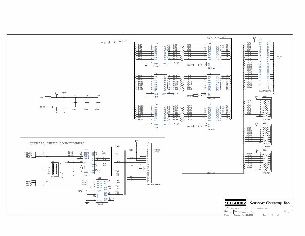
DIGITAL I/O SECTION, MODEL 7421
B4 4Tuesday, June 29, 1999
Title
Size Doc Rev
Date: Sheet of
Sensoray Company, Inc.
DIO0DIO0 DIO0 D0 DIO1DIO1 DIO1 D1 DIO2DIO2 DIO2 D2 DIO3DIO3 DIO3 D3 DIO4DIO4 DIO4 D4 DIO5DIO5 DIO5 D5 DIO6DIO6 DIO6 D6 DIO7DIO7 DIO7 D7 DIO8
DIO9DIO10DIO11DIO12DIO13DIO14DIO15DIO16
DIO8 DIO8 D0 DIO17DIO9 DIO9 D1 DIO18DIO10 DIO10 D2 DIO19DIO11 DIO11 D3 DIO20DIO12 DIO12 D4 DIO21DIO13 DIO13 D5 DIO22DIO14 DIO14 D6 DIO23DIO15 DIO15 D7
DIO0DIO1DIO2
DIO16 DIO16 D0 DIO3DIO17 DIO17 D1 DIO4DIO18 DIO18 D2 DIO5DIO19 DIO19 D3 DIO6DIO20 DIO20 D4 DIO7DIO21 DIO21 D5DIO22 DIO22 D6DIO23 DIO23 D7
DIO8DIO9DIO10DIO11DIO12DIO13DIO14DIO15
TA0+
TB0+TIMA0 TA0-TIMA1 TA0+ TA1+ DIO16TIMA2 DIO17
TA1- TB1+ DIO18TA1+ DIO19
TA2+ DIO20TA2- DIO21TA2+ TB2+ DIO22
DIO23
TA0-TA1-TA2-
TB0-TB1-
TB0- TB2-TB0+
TB1-TB1+
TB2-TB2+
D[0..7]
DIO[0..23]
DO0DO1DO2DO3DO4DO5DO6DO7
DO8DO9DO10DO11DO12DO13DO14DO15
DO16DO17DO18DO19DO20DO21DO22DO23
DO[0..23]
TIMB2TIMB1TIMB0
+5V
+5V VCC
+5V
+5V
+5V
+5V
+5V
+5V
+5V
+5V
+5V
RN2
10K-SIP
123456789
10
RN3
10K-SIP
123456789
10
RN4
10K-SIP
123456789
10
U18
2803
12345678
9
1817161514131211
10
D0D1D2D3D4D5D6D7
GND
Y0Y1Y2Y3Y4Y5Y6Y7
COM
U20
2803
12345678
9
1817161514131211
10
D0D1D2D3D4D5D6D7
GND
Y0Y1Y2Y3Y4Y5Y6Y7
COM
U22
2803
12345678
9
1817161514131211
10
D0D1D2D3D4D5D6D7
GND
Y0Y1Y2Y3Y4Y5Y6Y7
COM
C44
0.1uF
U19
74HC240
2468
11131517
119
181614129753
1A11A21A31A42A12A22A32A4
1G2G
1Y11Y21Y31Y42Y12Y22Y32Y4
U21
74HC240
2468
11131517
119
181614129753
1A11A21A31A42A12A22A32A4
1G2G
1Y11Y21Y31Y42Y12Y22Y32Y4
U23
74HC240
2468
11131517
119
181614129753
1A11A21A31A42A12A22A32A4
1G2G
1Y11Y21Y31Y42Y12Y22Y32Y4
P3
HEADER50MRS
135791113151719212325272931333537394143454749
2468
101214161820222426283032343638404244464850
P4
HEADER20MRS
1234567891011121314151617181920
C45
0.1uF
U24
26C32
12
3
4
5
67
8910
11
12
13
1415
16
IN0IN0
OUT0
E
OUT2
IN2IN2
GNDIN3IN3
OUT3
E
OUT1
IN1IN1
VCC
U26
26C32
12
3
4
5
67
8910
11
12
13
1415
16
IN0IN0
OUT0
E
OUT2
IN2IN2
GNDIN3IN3
OUT3
E
OUT1
IN1IN1
VCC
U25
SMDA05-6
123458
6
7
C46
0.1uF
D[0..7]
+5V
DGND
GDIO*0
GDIO*1
GDIO*2
TIMA1TIMA2
DO[0..23]
TIMA0
TIMB0TIMB1TIMB2