semiconductor equipment bmmmmmmmmi eeelleeeeeelll
TRANSCRIPT

DR137 598 MICROWAVE SEMICONDUCTOR EQUIPMENT PRODUCED IN POLAND i/i(U) FOREIGN TECHNOLOGY DIV WRIGHT-PATTERSON AFB OHJ KLAMKA 28 JAN 84 FTD-ID(RS)T-1884-83
UNCLASSIFIED F/G 9/5 NLbmmmmmmmmiEIEEEIIEEEllEIEEEllEEEEEElll

11.
111112 1.0 _.0
NATON L BURAU OFSADRS16-
11111[25 ~ 11
%5

FTD-ID(RS)T- 1884-83
11 FOREIGN TECHNOLOGY DIVISION
1 MICROWAVE SEMICONDUCTOR EQUIPMENTPRODUCED IN POLAND
by
Jerzy Klamka
CDTIC• IELECTE
Approved for public release;
distribution unlimited.
V CO84 02 07 011# -:V?'' - . "'S "" * V ' ;' ... ' T ' :* -, ": :,

..
,I.
FTD-ID(RS),-1884-83
EDITED TRANSLATION
FTD-ID(RS)T-1884-83 20 January 1984
MICROFICHE NR: FTD-84-C-000083
MICROWAVE SEMICONDUCTOR EQUIPMENT PRODUCED INPOLAND
By: Jerzy Klamka
English pages: 32
Source: Elektronika, Vol. 21, Nr. 1-2, 1980, pp. 44-54
Country of origin: PolandTranslated by: LEO KANNER ASSOCIATES
F33657-81-D-0264Requester: FTD/TQTRApproved for public release; distribution unlimited.
I THIS TRANSLATION IS A RENDITION OF THE ORIGI.NAL FOREIGN TEXT WITHOUT ANY ANALYTICAL OREDITORIAL COMMENT. STATEMENTS OR THEORIES PREPARED BY:ADVOCATEDOR IMPLIEDARE THOSE OF THE SOURCEANDDO NOT NECESSARILY REFLECT THE POSITION TRANSLATION DIVISIONOR OPINION OF THE FOREIGN TECHNOLOGY DI. FOREIGN TECHNOLOGY DIVISIONVISION. WP.AFB. OHIO.
FTD-ID(RS)T-1884-83 Date 20 Jan 19 84
GRAPHICS DISCLAIMER
All figures, graphics, tables, equations, etc. merged into thistranslation were extracted from the best quality copy available.
Accession For
DTIC T"',, Unann,..n-[
I Di str ib1t ion/
Availability Codes
Avail and/orDist Special
N
... , ., g ~ , - - S .* S. * .€ . S. . .>, W * q..- -. , . . ,; ; .: - ; ¢ , - . . : . :- : . : : : . : .,
- 7 -
MICROWAVE SEMICONDUCTOR EQUIPMENT PRODUCED IN POLAND
by Prof. Dr. Hab. Jerzy KlamkaThe Electronic Technology Institute of the CEMI, The DiscreteSemiconductor Equipment Section 4
A
In 1978 we celebrated the 25 year jubilee of continuous
development of Polish radar. The development of this field of
technology, so important for the national economy and national
defense, is dependendent upon designs and production possibilities of
subsystems and microwave elements used in radar equipment. Playing a
key role among these are microwave semiconductor devices (MPP)
produced in Poland.
As in the leading countries of the world, work in the fields of
the theory, design and technology of microwave semiconductor devices
has been carried on for years in Poland. The designed equipment has
been closesly adapted to the newest devices produced by our radar
industry. These devices are designed and produced in the Discrete
Semiconductor Equipment Section of the Electronic Technology
Institute of the CEMI.
The History of the Development of Microwave Semiconductor Devices
* The work on microwave semiconductor equipment was begun 20 years
ago. Research was started on varactors for parametric amplifiers,
which took place in the Institute for Basic Problems of Technology of
the PAN [1. The research unit, which performed the research there,
increased with time, leading subsequently to the Electronic
Technology Institute of the PAN and finally to the Electronic

Technology Insitute of the CEMI. At the same time, together with an
expansion of the themes connected with microwave equipment, there .E
appeared larger organizational units, such the laboratory, then
* .institution (1970) and the section in 1972, in which besides research-
developmental work, small serial production of the microwave diodes
was also undertaken.
In the history of the development of microwave semiconductor
devices it is possible to discern several characteristic stages.
In the first of them, in the years from 1959 to 1967, work was
carried out on the design and technology of varactors intended for
parametric amplifiers and harmonic generators. As a result of this a
series of types of germanium, silicon and gallium-arsenide varactors
were produced [2-141. These varactors were used for example in Avia A
and Avia B radar. The working out of the production of varactors inshort series in the IPPT-PAN started off application work both in
industry (PIT, WZR Rawar) and in academic centers. This was,
consequently, the beginning of the development of microwave
semiconductor electronics in Poland.
The second stage of UPP production, between 1968 and 1974,
encompassed a significantly broader theme than had been the case in
the previous period. Besides work on the newest types of silicon
varactors [15] research was performed parallely in the field of
avalanche diodes [16-201, PIN diodes (21-251, Gunn diodes [26-271 and
Schottky diodes [281. Work was also performed in the field of the
microwave surveying of the basic parameters of the mentioned types ofdiodes. As a result of this the following types of technology wereproduced:-- PIN diodes intended for work in the S and X bands, used successfully
2
!'I

for example in scaled microwave systems produced in the PIT;
--several types of avalanche diodes intended for work with constant
power in the X band (with an initial power within the boundaries of 50
and 750 mW);
--two types of Gunn diodes with a constant power in the X band between
50 and 250 mW; also designed were;
A--the first models of the Schottky diode in the S and X bands;
--a technique for measuring the microwave parameters of the above
mentioned diodes. A series of measurement heads were also designed
and produced, and a series of varactors for the needs of the PIT and WZR
Rawar (some of them were produced for export) was introduced into
laboratory production.
Deserving of special attention is the fact that technological
work was performed at that time with the aid of atypical and rather
crude apparatuses. Nevertheless, the varactor production was
organized and begun in such a way as to completely meet the national
need in the field of the produced types of these devices. Also
produced in this field were models of all the necessary types of
microwave diodes (avalanche, Gunn, PIN, Schottky) anticipated for
radar equipment designed in the PIT. Some of these, such as avalanche
and PIN diodes, were produced in short series and were used in various
microwave systems.
This was, therefore, a very fruitful period in the development of
microwave semiconductor devices, regardless of the shortages of
apparatuses in national institutions [291. An entire diode thematic
was worked out. The diodes produced, subsequently, stimulatedapplication work both in the radar industry and in other scientific
centers in Poland, which were occupied with microwave technology.
3

The next two and a half year period (the end of 1974 to the middle
of 1977) was not very fortunate for MPP development. Organizational
and cadre changes were instituted in the national "Microwave
Institute" and support for its activity (in the technological field)
in cooperation with the wMicroelectronic Institute had to correct the
situation and create new possibilities for MPP production. This did
A not lead, however, to the expected results. As a result of this,
production of varactors manufactured according to older methods fell,
and the modernization of their production with the use of line
technology (intended for the manufacture of scaled systems) did not
ensue. In this period no new microwave devices were produced.
Prepared prototypes of new diodes, although based on achievements of
earlier periods, required basic design-technological modifications.
The Newest Achievements of the DH Section in the Field of MPP 45
In June 1977 on the basis of the Microwave Institute the Discrete
Semiconductor Device Section was founded (DM section), in which
research and production in the field of KPP was chiefly undertaken.
Contrary to the earlier period, the DX section possessed to a greater
extent its own modern technological equipment. This created the
possibility of the more rapid production of new microwave devices.
This also allowed the modernization and increased efficiency of the
production of already existing microwave diodes.
The new conditions and possibilities, as well as the
organizational and cadre modifications carried out in the the DX
section, led to the rapid progress of research-developmental work in
the field of microwave semiconductor equipment, as well as an increase
in the size of its production. In the course of two years a series of
new types of microwave diodes was designed and introduced into
4

production (table 1), the production of these diodes was radically
increased (illustration 1) and the technology of the older types of
varactors, which functioned until 1974, was modernized.
All the new microwave devices correspond to foreign diodes and
are characterized by the required reliability. They also hold up
under harsh mechanical-climatic conditions. Modern production
technology guarentees their greater reproducibility and decreases
labor requirements. This has resulted in increased laboratory
production capacity, as well as a decrease in personnel needs.
The production level achieved in 1979 meets the needs of the
Polish radar industry in the field of the mentioned types of microwave
diodes.
The development of Polish radar has led to the further expansion
of the venue of the DM section. Besides traditional diode thematics
and microwave survey, work is now commonly carried out on transistors
and microwave subsystems.
The results of the labors of the DM section connected with the new
devices and microwave subsystems introduced into production are
presented in another part of this article. The parameters of all the
commonly manufactured microwave products are also given.C
5
i.

. .1 .-- i . 4 15..'1 4
" Ww~k tnry 93:D- 14 RXDP-1l4 BXDP- 14
SB3IDP-4s BXDP-43 BILDP-43BXDP .4. ..DP- 44 BIX.D1P- 44
xIpr-3 JBXDP -*S BXDP-45,. J[ktrI~ '-u ! BXDP-51 BXDP-31
BXDP- 2 BIDP-5-BIDP- 74 BXDP-"4
DiY Gu'- CXDP-44 .xDP-43
0 CMDI' - 44
Diody Ml bA. DP-2
31I~?-74 5IP-24
BADP--4
DAEP -. I
I Diodr - - BADP-1 6fI S ot tkyu'eu )iAri' - 1.
k.nre -- DX DI' -b
*-Ge -t , GFX-0 1
SGUna GFlE-402
14*WA tug.) w nmub4W diw ips b.i!r bmiuj podtpl. ktftydb paaVat pdaw V ,dnp,* v : tablrh:
1q 8) pmdtlpr &-. a b, I bt a c' .'u a daiotam m ed-biffe%- bw 6Mta 4 a9W-U
Table 1. Basic types diodes and microwave subsystems laboratoryproduced in the DM section between 1977 and 19791. varactors, 2. Gunn diodes, 3. PIN diodes, 4. Schottky diodes, 5.avalanche diodes, 6. Gunn generators, 7. production year, 8. Note, 1)within the framework of a given type of diode there exists subtypes,whose parameters are given in other tables, 9. 2) subtypes of diodeswith the letter Y in their designation are supplied to the consigneewithout special attestation
6
_- V-

a)
%it I
I l u t a i n II h n c e s n t e a n l p r d t o n f mi c r w v
~1
r
b)
0! 74V 19?Se 1976f.' 1977r. l97? 179
Illustration 1. The increase in the annual production of microwavediodes: a) in relation to the 1974 level; b) in comparison to thelevel of employment
Illustration 2. Microwave diodes and semiconductor transistorspresently produced in the ITE (DM section)
The Construction and Assembling of MPP
' - ' ,, I r , ' .,, . '"-; ; .' , ; " - ' .' 2 :'"; ." "". . ..: ' ':-: ' •".-. ' ' 7'.i-.
" -.i..:
'I
Microwave semiconductor diodes developed in the Institute are
for the most part produced in the 0C4 housing according to"" international standards. The majority of the types of varactors
have, however, other kinds housings. Their design was worked out in
the ITE ten years ago [9, 13]. The diodes in such housings are used asbefore in many systems produced in Poland. In illustration 2 is 47presented microwave diodes, which were manufactured in different
housings. These are ceramic-metal structures with an alunduminsulator. Their schema together with their dimensions are given in
illustration 3.
OCN* OCNIP OC4P
C2'
VN L
,o 2 374 J_ ,, 46 2.
OC2
T-plasfykOC 7 52S Max 5 9
30
,o.oI ,= ._ , '
4, -i
illustration 3. Housings of microwave semiconductor devicesproduced in the ITE (DM section)
8
,, ,- ,, . -".--. - . - .. .,. %.- -, . . -,- - - -. . . . .. . ." . .. .. .-_i . .e~ .: . ,j ., #.L _ _. • 4'., !,., ., ,. .. ,. . , .,.., .,..,,....,..,{,..

N.
a)
fobcae mirwvesse) ;d exaple of th stutr
22
35
2 5'3
Illustration 4. Design examples of microwave diodes: a) a design ofa diode with a linked contact (1--solder, 2--electrodes, 3--linkingelectrode, 4--structure, 5--ceramics); b) the structure of a diode
paste)
Despite the many types of housings, the connected structures are 47
mounted in them in a twofold manner. All housings, wi the exception
of the OC4, have a design anticipated for the assembly of a structure
in a mesa form, with the part contacting the top in the form of a metal
bowl. The diode's assembly is very simple here. This leads to thefact that on one side the structure is soldered to the housing's
support (depending on the type of housing with the different forms).
However, from the ohe es aic it is inserted into the housing
connecting the electrode. Situated on its end an elastic, phosphor-
bronze coated chip, resistant to shock, ensures good contact with the
structure's bowl. Then, the end of the housing's upper electrode is
soldered, which immobilizes the inside electrode and encloses the
diode. An example of this assembled diode is given in illustration
4a.
The assembly of the diode structures in the OC4 type housing
9
,.,. - v --.-..
* - , . ,. . , . > : . ,: . . , . . L : .:; ;/ - - "I' *.I
requires special equipment. The structure after soldering to the
housing's support is connected to the housing's collar by gold wire.
Both of its ends are welded by thermocompression or by ultrasound.
The diode's enclosing follows after the welding of the upper electrode
Y(the cap) to the housing's collar (illustration 4b).
In the case of scaled microwave systems, welded structureswithout housings, which have passive layers of oxides on their
surface, are often used. In this case such structures with connected
gold conducting wires are delivered to the consignees. They are next
mounted directly in the microwave striped line (illustration 4d).
The connection of the base and the structure's conductor can be
performed by aid of a special paste, which conducts current well.
Microwave diodes in the housings presented here are resistant to
shock and acceleration. These devices are resistant to vibration at
frequencies of 10-150 Hz at 25 g.
In illustration 5 the first structural design of microwavetransistors worked out in the Institute is presented. It is intended
for work in frequencies up to .9 GHz. At such frequencies it is
possible to use plastic instead of ceramic insulators, necessary for
all frequencies, taking into consideration the greater loss in the
microwave band. The assembly of a series of transistor structures
procedes in an open-work form (illustration 5). The next process in
the stamping plant is the formation of plastic wafers, in which the
structures are sunk (illustration 5b). The transistors from the
open-work stripes, whose external appearance is presented in
illustration 5c, are cut out on the end. The transistor housing's
supplementary schema and the values of its parameters are given in
illustration 6.
10
I I..
a)
II
5*5
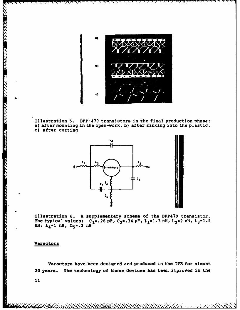
Illustration 5. BFP-479 transistors in the final production phase:a) after mounting in the open-work, b) after sinking into the plastic,c) after cutting
~L5
Illustration 6. A supplementary schema of the BFP479 transistor.The typical values: Cl=.28 pF, C2 -. 34 pF, Ll-1.3 nH, L2 -2 nH, L3-1.5nil, L4-1 nil, L5 -.3 nH
Varactors
Varactors have been designed and produced in the ITE for almost
20 years. The technology of these devices has been improved in the
11

direction of increasing the reproducibility of parameters and
decreasing labor consumption. New types of diodes with improved
electrical parameters have also been designed.
Until recently, all the types of varactors produced were based on
the p-n microjunction, whose design was worked out in 1965 [11]. This
4. is dependent on the formation of a bowl of smelted Au-Ge eutectic alloy
on a Si chip coated with nickel, which contains the p-n junction made
by a diffusion technique. During the etching of the chip's surface,
the bowl protects the part of the junction placed beneath it, and
during assembly the varactor makes ohmic contact with the spring
located inside the diode's housing. This method allows that in case
of the lack of typical or costly equipment the p-n junction can be made
for microwave diodes, as well as simplifying assembly. Such
junctions (illustration 7a, b) are made individually. The bowl is
made individually and every junction is etched individually.
Depending on the initial material, structures for varactors used in
parametric amplifiers, as well as for power varactors, intended for
harmonic generators (multipliers), are made in this way. Structures
connected to the first of the mentioned group of varactors are made
from p type silicon {9 3.10-3 Lacm), although the remaining
structures are made based on type n epitaxial layers (the choice of
resistance is conditioned by UBR) [9].
In connection with the considerable expansion of the production
of varactors, the most labor intensive aspect of their production has
4 been modernized. The technology used in some types of varactors
allows the simultaneous production of the microjunction. This is
made on a larger silicon chip, containing the p-n junction before its
cutting into the structure. This has become possible thanks to the
introduction of thermal oxidation, photolithography and "inset"
etching in SiO2 layers, where the microjunction has to be made. As
12
,k1
before, the nickel layers, which make ohmic contact, are placed in 48
these places of the silicon's surface. Next, layers of gold and- stannum of corresponding thickness are placed on this layer. After r
heating, the Au-Sn layers form the bowl with a eutectic composition.In order to ensure good contact with the spring of the diode's housing,
the bowl's surface is coated with gold. After the etching of the
chip's surface around the bowl several microjunctions with equal
electric parameters are obtained simultaneously. After the chip'scutting individual structures with similar geometry are obtained, as
previously had taken place (illustration 7b).
BXDP-14 and BXDP-51 varactors have already been produced in the
given manner. The electrical parameters of these diodes are given in
tables 2 and 3. Further steps have been taken within the framework ofthe modernization of varactor technology and the correction of their
exploitation parameters. Planar technology has been used in the
production of these devices. The new BXDP 52 varactor, which has a
miniaturized OC4 housing, has been designed on the basis of this.
This varactor with regard to electrical parameters corresponds to theBXDP 51 varactor, but is mounted into a smaller OC4 housing according
to international standards. This new varactor has better electrical
parameters (table 3) and is easier to produce.
The planar junction structure is made with the use of moderntechnological processes applied in these cases. This ensures a
greater reproducibility of parameters, decreases labor consumptionand considerably increases output. During the technolgocial
process, the junction structures are thermally made passive by
oxides, which ensure greater resistance to the diodes' external
exposure, as well as increasing their stability and reliability.
13
. . - .- ---'.." -----

Table 2. Silicon varactors for parametric amplifiers in the L band1. diode type, 2. junction capacitance C 0I at UR=0, 3. capacitanceratio, 4. penetration voltage UBRat 1R=10,AA, 5. cut-off frequency fcat UR=-6V, 6. total power Ptot at tumb=250 C, 7. heat resistancethj -c, 8. housing type, 9. or
t*,4ljvmift
. . .. .-a.. _ . _i
Z can 2W r'__ -' W 9 oabpw
0- so~" r'R_ CP "a s
2JLDP1 I IL0 so 2 I 00 OCL'n" tub
3.IDVIS U 1.2L11 2_ _ _ ___ __ __00____
"IIkxY I4 1-34 2 O OC.I
Tafle s3• Silicinvaractors for frequency multipliers in the UKF, L, Sand X bands1. diode type, 2. junction capacitance C._6 at UR=-6V, 3.capacitance ratio Cjo/CJ_ 6 at UR=O and UR=-6 V, 4. penetration voltageU at Inc0 A, . cu -off frequency f at UR=- 6V f=3 GHz, 6. totalUBRa S.l band, 9. houinpower P tm=250 C, 7. heat resistance Rthj c 8. band, 9. housingtype, OL.4oe: the BXYP43, BXYP44, BXYP5, BXPY52 diodes and theirsubtypes also have the same electrical parameters, as well as thosewhich correspond to them, but are delivered without specialattestation, 11. or
own"m I
TYPOv 2d d e"I- ChIC,. 4 PW Can PW po WFm'bo POS-4 C -- 6V IM uv Rpi 1SpA .-iu. '
[p71 (pV'pI ( lGNu [WI lwc Wl
INDIO 2I3 . -I5 4 18 ERF.L OCT.
DIflDo3.-.53 2 Ii L OCI__
BXDP46A U-93 2.3 - 49 S 0u4I~I.DI 3.-LB3. U i Ml t OS S Il ( (I31IF410 U-I.A 3.1 UO a I t a s 0o
IDPIIA - Ift 04 LB I X O '4 kb I/t
IDINA. 5.-Si U0 i 1 0.5 118 1 0va41Jb
I=DiPm O.5-0 £ U 11 1.5 IN X 0C41
(0 r : di MXlll b 11TPm 3J115. &INTPh. INIYNI wi M sot iWf Wsm d i 3 JoJak kb S/IW iW,+ fII. 11w, um _ . ....... 1
1J1
',, .. ", ".. . ," . •".."".".. " ."% ,," ."." .".....-.. '.. , " .. .. . * 4' - *.. - -.. ,,'' +
?%J - wm 3 pojmNis Ma - Wu I* Moe . a Reqs"misTyp &4yr M Imdc fi ran. PM M- I a I - i V I -.is Typ obudow.
([YVJ MOa log MWJ 11CMW
BXD741 0.8--i 3.9 40 90 3M 80 OC4RXDPT45 0,-U 3.9 40 lo 3e so OC4BxEP, O.8- .i 3.9 40 UN) struktam zwoo-
us (bez Obiido.) 9* .XYP74A 0.6- IA 8.7 40 90 300 100 (WA
XYP7 0.6-1* 3,7 40 100 200 100 0,4
Table 4. Silicon varactors for ger.-rator change-overs and microwavefilters1. diode type, 2. junction capacitance Cj_ 4 at UR=- 3 , capacitanceratio C. /C. 20 at U = 0 and UR=-20, 4. p netration voltage UBR atIR-10 , . cut-ofF frequency fc at UR=-4 V and f=3 GHz, 6. totalpower Ptot tu b-250C, 7. heat resistance Rthj-_l 8. housing type, 9.junction structure (without housing)
The structure of the BXDP 52 diode ensures better heat offtake 48into the housing, through which a considerable reduction of thermal
resistance in comparison to the value of this parameter in the BXDP 51diode is obtained. The values of the parasitic parameters are also
reduced. The inductance and capacitance of the OCN4 housing are 49
contained within the limits of 1.2 nH and .30 pF, when in the OC4 this
does not exceed .8 nH and .25 pF [30,31].
A sketch of the technology of the varactor's planary structure
follows. A SiO 2 layer is formed on the n type epitaxial layer t-. 35Q cm, he-4.5 *im), installed on a strongly doped base (L <10 - 2
£Qcm). Next, after the use of the photolithographic process and
etching, an inset (ff=70.Atm) is formed in the insulating layer, by
which the boron's diffusion is accomplished at a depth of 3Am. Thep-n microjunction is created in this manner. In subsequent processes
a contact suitable for the p type layer is created in the inset byinserting the Pt, and then adding Cr and Au layers. After part of thebase is ground down, a nickel contact is formed. In this way several
hundred structures can appear simultaneously on one silicon chip.After the chip's cutting individual structures are obtained
(illustration 7c), which are mounted in the OC4 housing.
15

The technology of junction structures used in varactors intended
*for the change-over of microwave circuits (BXDP 74, BXEP 74) was
designed individually [32,331. The p-n junction was made here at a
depth of around 3 m as a result of the diffusion of boron in the
layer's epitaxial part (e =.4. cm and a thickness of around 4
m) inserted on a strongly doped base with a resistance on the order of* 10-3 A cm. The junction structure obtained in many of the
technological processes has the form of a covered mesa, which makes
the SiO2 layer passive (illustration 7d). The varactors from this
type of structure obtain a greater cut-off frequency and more useful
capacitance-voltage characteristics than planary varactors. The
effective protection of the p-n junction's flange used against
external influences guarentees the varactor's good electrical
stability. With BXDP 74 varactors, the structures are also mounted
in the OC4 type housing.
The passive junction structures, with a junction in the form of
gold wire, are intended for use in scaled microwave units, such as the
BXEP 74 discrete changing-over varactor.
The electrical parameters of the 74 series of varactors are given
in table 4.
A
0) d°)
1I6
'll " ."k *- t
-io $. SOO ~~*.~~ L*~** ~ . .. ~ *

4- I
not. k
" .. b)I) /I)
k)
, Jr
Illustration 7. Junction structures used in microwave diodesproduced in the ITE: a) the p-n microjunction of a varactor with amesa form with a spherical contact; b) the p-n microjunction of a powervaractor with a spherical contact; c) the planary structure of avaractor; d) the junction structure of a varactor with a mesa form; e)the junction structure of a p+-v avalanche diode; f) a structure with aSchottky barrier; g) the junction structure of a low power PIN diode;h) the junction structure of a high power PIN diode; i) the structureof a Gunn diode with one epitaxial layer; j) the structure of a lowpower Gunn diode with a triple epitaxial layer; k) the structure of aGunn dode with one epitaxial layer; 1) the structure of a Gunn didewith a triple epitaxial layer: n4 (k)--the n+ type epitaxial contactlayer; nM(b)--the epitaxial buffer layer, k--the ohmic contact, b--the buffer layer, --the area of the type n autonomoussemiconductor, i--the area of the autonomous semiconductor
Avalanche Diodes
Avalanche diodes, besides varactors, are intended for
multiplying a signal's frequency.
The function of these diodes rests on the storage effect of the
smaller axis carriers near the p-n junction, introduced during the
diode's conduction, and then on their rapid regeneration when thediode is polarized in the reverse direction. As a result of this a
greater impulse of current is obtained in the reverse direction, as
well as its rapid decline (less than 1 no). This allows the greater
product of the frequency multiplication in one level of the
multiplier. Contrary to multiplication by aid of varactors, where
17
I 1 : ' I
" " " " ° ' ' "
"'" ' ' ' "
"'-' ' "* ' • °
' ' ' ' ' ' " " , . -" "
the multiplication's efficiency declines with the increase of the
harmonic order (n) to the tune of 1/n2, multiplication by using
.9 avalanche diodes is more advantageous. The efficiency of the
harmonic generators here decreases proportionally to 1/n (with n>5
[12]).
Research on avalanche diodes, performed in the Institute, has
led to the designing of these diodes' optimal technology.
Avalanche diodes (BXDP 82), which have been introduced into
laboratory production, have a p+-v-n+ mesa type junction structure,
covered by a SiO2 insulating layer (illustration 7e). The technology
of this type of structure is similar to that of structures from
illustration 7e. The difference depends on the technological
preparation of the silicon chip before the mesa is formed. The
initial material is a strongly doped base (1019 at. cm-3) with an
installed epitaxial layer with a resistance of around 100 rL cm. Thechip is made for this layer by boron diffusion. The proper choice of
the geometry of the material's structure and the technologicalprocesses allow the creation of a junction structure with a suitable
doping distribution, which forms an inhibitory electric field in the
junction's region. This field gathers around the charges of carriers
introduced during the diode's conduction, which after the
polarization's change is rapidly removed, creating a right angle
impulse of current.
The electrical parameters of the BXDP 82 avalanche diode are
given in table 5. Special attention should be given to the value of
the the cut-off frequency and very small transition time tt [34].
18
, - -t. . . .- .,, ... -, .*,*..9 . ?, . %* ,. ' ~: .-: . '

71. Ir. -a--- -i "W1r.-
I Mug, £t 1wa
dV VWUMe~ P,, MY rrTYP fpdy C"14 v prAauw .i ww A 1W 5, /Q P Rtis
1r---. . caN.er -IOwA -6 -II" 4 Gas W' or 1ieo pr~eiwl I"~ Ip- * 'JA
'mw Ia- -'.Inv)pt' [Ii Lt Ea !,ml LWl ! ".i ;
IZD i 1 -3 " I s le O.l $ 29 IW4BITNI 1 -S U 10 n.il - .,, w' a
Table 5. Silicon avalanche diodes for multiplying frequencies in the 50S and L band1. diode type, 2. junction capacitance C .6 at UR=- 6 V, 3. penetrationvoltage UBR at IR-10JM-A, 4. cut-off frequency fc at UR=-6 V, 5.transistion time t at I=10 mA U -10 V, 6. total power Ptnt at aconstant conduction current t Imb:E°C, 7. doubling efficiency atf w 4 GHz, 8. effective life of the small axis carriers at IF=10 mAIR16 mA, 9. housing type, 10. heat resistance Rthjc
SI d3: ft "We 9. MSO W 'i*mTr eg-e "Now 1'_W XM Fo Z.-n =9410a
Fora- fow-30MZ C P-1 UW P-I U. W,.. tWXfY .Ud"ir
1= ORDi J 1-3 Gib f-2 Gus NofpNEI :dil IQ] I"T !rW1 :-#I
buIw
ZATIMI U O o-mo * U __S _4
Table 6. Schottky silicon diodes for mixers, which operate in the Sband1. diode type, 2. junction capacitance C at UR-0, 3. cut-offfrequency fc at U -0 rs at If -20 mA, 4. total nA1se coefficient f cz--30MHz f-3 GHz, 5. limpedance tZt for: fz-30 MHz P-I MW f-3 W 6.coefficient of the standing wve Sv Xt Zo-50 P-1 mW, f=3 GHz, 7.continuous wave power Pw, 8 sharp impulse energy W1 at t-2.5 ns, 9.housing type, 10. junction structure without housing
19

-. - ,W .7 . . . ., ' .-..
bNOV
'2. ,18JIiMM5 b.. Wep-ksnaalk OWWW11 9V iapbu & al l.m P. Pus7 twith~bim Reys
Ir ombwit CIts Io vi 4,14S. my MkUl P "~* C.... PrL- *enukm obudl-3 CT -MY MY R, uRIF IF 10
mA M4 'R-O Pr&1 :ilaa iV*0 M.mIom WYos~y% t-O&Ar f-t IM rI-0V IF-IA IR- tUre i -u R wI f-1 ~ RL-1U 00t
____l (p71 A_ _'04 IV Vl I I "Il Wl [ C w1
DADP
D ? oo~. o. 1.5 .___ . s , oo C4no1 0.71 OA5 I A-". 5 0
- Table 7. PIN silicon diodes for commutators and limiers1. diode type, 2. penetration voltage UBR at IR=104..A, 3. totalcapacitance CTO at UR-O f-i MHz, 4. total capacitance CT50 at UR=50 V 50f-i PH, 5. resistance R. at Ip=100 mA, 6. commutation time trr atIp-100 mA IR=500 mA, RL=100, 7. coefficient of the standing wave So atUR=0 f -1 GHz, 8. total power Ptot at the constant conduction currentt -250 C, 9. microwave power PMais at impulse operation, 10.tiermal resistance Rthj.oc, 1. housing type,
, I_ im m Kabyigah ; Soba"boern t 3 ZAM m XWWY". Nabyrmmb
i LVI (91 11 taw I' NKul 1 f1111.VJ IT] liiAl I _C
CXDIP4A O*0.8 V 113-10.5 15 t5 10 70 O C4o
CXDP483 I 1"$AUV 9.-U 16 13 is - 40 - 70 OC4
CIDPIS 8-12 0.- -L.4 10 10ow ii41 - -100 DC&
LIT. 43-1 -12 6-12 11°
i2 111 1 In .3 (W4UXTP43-2 0-12 11-12 1W 60 53 0(4' 4---a i I aO -20 0(4
CIlIM- 4-12 4-1 18 - 40 - 100 *4
CX o-a i -n a-ia 100 It -. , - IOl c C4
fUwW: pasmef obf do im pW Me*w W Wv*W*a 111MMUffa kamulali.. dks klidw &Y5 JAY.
Table 8. Gunn diodes intended for microwave generation in the X band1. diode type, 2 .nominal amplification voltage Uo , 3. frequency rangef, 4. minimal initial power P , 5. changing-over range f, 6.maximum sensitivity of votalge cNanging-over f/ Uo , 7. maximumamplification voltage UO~ax , 8e maximum amplification current 1 0 119. temperature range of the surroundings during operation tamhousing type, 11. note: parameters are determined during the des'operation in special generators controlled for each type of diode
Schottky Diodes 51
Work on Schottky diodes has been carried out in the DH institute
for six years. In this period a series of technological versions and
models of these types of diodes intended for operation in the S and X
bands has been developed. A Schottky contact based on a silicon-
silicide platinum circuit was formed in these diodes. It is
characterized by a considerable heightening of the potential barrier,
20
............ % • . . ,, " ,' . % ' - .. .l l i I U I E M i I ! : ::- IS.

which is not advantageous from the point of view of the diode's noise.
With regard to this, recently there was designed new technology,
thanks to which a relatively low potential barrier can be obtained.
This has become the basis for the structure and technology of a
prototype of the BADP 14 silicon diode (and its modification, the BAEP
14 for scaled microwave circuits). The mentioned diodes are intended
for operation in a mixer system in the 1-4 GHz range.
The structure with a Schottky barrier (illustration 7f) is
realized by an epiplanar technique. The intial material is a silicon
base chip with a <111> orientation doped with arsenic (e =.o1
* cm), on which is formed an epitaxial layer doped with phosphor L =.3
cm) with a thickness of around 1 X m. The metal forming the Schottky
barrier on the silicon is infused in a 10- 7 Tr vacuum through the inset
in the SiO 2 layer. Then, the gold layer is placed in this same way,
which faciliates the barrier's connection with the housing. The
mentioned insulating layer with a thickness of .6 As..m is formed in the
process of the silicon's thermal oxidation. The inset with a
diameter of 20O.m is made by a photolithographic technique and
etching. The appropriate base contact is made by the infusion of
several layers of metal. The first of these forms the lower metal-
semiconductor junction, the other layers of gold permit the easy
connection of the wire structures with the housing. Good results are
*obtained by using chrome as a contact layer.
A series of junctions with the Schottky barrier is found on the
silicon chip mounted in the housing, although only one is used. These
are reserve junctions, which can be used if the first of them has poor
characteristics, which statically arise with an inaccurate
connection [351. The electrical parameters of the BADP 14 and BAEP 14
Schottky type diodes, which have already been produced, are given in
table 6.
21

PIN Diodes f
Presently, two basic types of low and high power PIN diodes are
serially produced (the BADP 26 and the BADP 23). They are chiefly
intended for commutators and microwave limiters.
Silicon with a resistance of 1000 A cm is the initial material
used for the production of low power diodes. It serves as a base, on
which a layer of strongly doped n+ with a thickness of 150JLm is
formed in the epitaxial process. Behind the base's opposite side is
. formed the p+ region as a result of the boron's diffusion (5M.Xm).
Before the base's diffusion the chip is thinned to a thickness of 15CAm
4
The junction structure of a low power diode has a mesa form, and
its flange is covered by a SiO2 layer (illustration 7g). The
technique of forming this type of structure is similar to the
technology of the structures of BXDP 74 varactors.
High power diodes with a great penetration voltage and low
thermal resistance have junctions whose surface is several times
larger than that of low power diodes. This facilitates the formation
of the junction structure. In this case, it is not necessary, as it
was before, to decrease the surface of the active region in the chip
and to form a microjunction on it. The active region here is under theentire structure's surface in the form of square chips, as inillustration 7h. Honocrystaline silicon chips with a resistance of10 kQ).cm are the initial material, which is independent. Both the
22
' +-'llw '* -.. " ' + , ."** VF ( " €/ -"" "."" * .j* '.**-% **

p+-i and i-n junctions have a thickness of 7 and 30 Am,
respectively, and the chip's total thickness is 130 ,At m. The ohmic
contact for both sides of the chip is made by a currentless method by
the inclusion of a nickel layer. Both sides, moreover, are gilded
electrolytically in order to facilitate the diode's assembly. After
the chip's cutting into structures with sides of 500 Am, they are
* lightly etched on the flange. Both types of structures are mounted in
' the OC4 type housing. In BADP 26 diodes, the structures are soldered
to the housing's support, although in the BADP 23 diode they are weldedon. Behind the other side the chips are connected to the housing withgold wire [36]. The electrical parameters of both types of diodes are
given in table 7.
Gunn Diodes
The technology of Gunn diodes with a power between 50 mW and 250
mW, which operate with continuous waves in the X band, was designed in
1973 and 1974. A complete system was prepared then for laboratory
production of these devices, and basic circuits for the measurement of
the microwave parameters of these diodes was set up [26, 27, 37].
In 1978 prototype tests were finished and two basic types of Gunndiodes, the CXDP 43S and CXDP 44, were introduced into laboratory
production. The first type of diode, produced in two variations (theCXDP 43A and the CXDP 43B) were intended mainly for Gunn generators.
These generators were used in navigational and surface radar, which
operated at various frequencies in the X band. They can also be used
in other generators. The electrical parameters of the Gunn diodes
presently produced are given in table 8.
23

The technology of both types of Gunn diodes, with a power between
20 mW and 100 mW, rests on earlier technological designs mentioned in
the beginning of the article.
In the 0430 series diodes the active region in the GaAs chip is
found between the ohmic contact's island ( 80 Atm) and the strongly
doped base illustration 7i). The epitaxial layer has a thickness of
around 10 m and a doping level of around 3 x 10¹⁵ at.cm-3. A Ge-Au
eutectic layer infused with a 10 percent Ni doping, with a thickness of
a few microns, makes up the contact. A thin layer of gold (.5A9 m) isplaced on this layer, which facilitates the diode's assembly (a wire
connection between it and the housing). The ohmic contact is made
behind the chip's opposite side in a similar way. A GaAs chip
prepared in this way has the following dimensions after cutting:
400x400xlOOA m. It is mounted in an OC4 housing. The chip is
welded to the housing base from the mount's side by aid of a eutectic
alloy of Ge and Au.
In the newer series of diodes gallium arsenide with a triple
epitaxial layer is used. The layer of the active region has
.parameters similar to those of the "43" series of diodes. Behind both
sides of this layer are found contact and buffer layers, which
increase the homogeneity of the active region and the diode' s contact.
In this case, after the island's infusion, the GaAs region is etched
around it and a lower mesa form is obtained (illustration 7j).
The structures used in higher powered Gunn diodes have similar
material parameters and type of ohmic contact. The existance of
differences depends on the size of the active region and manner of the
chip's mounting in the housing. The ohmic contact on the entire
surface of the GaAs chip is infused here behind both sides. Then, the
24
&A.................................. AA . ..

larger chips prepared in this way are cut into structures, which have
sides of 200Am (illustration 7k). The structure is welded to the
housing's base from the cathode's side (opposite to the previous
case). Around a ten times smaller thermal resistance is obtained in
this manner in relation to that, which diodes with chips welded to the
housing from the mount's side have and five times greater intial power
than that of a Gunn diode.
Recently, chips with a triple epitaxial layer have been used
(illustration 71).
Avalanche Diodes.
Avalanche diodes have never been produced serially, although
their technology was designed a long time ago [20]. This results from
the insufficient need for them.
'U*J1
25
I0 84&
-. * .. * . * - ,, . .° - . 4 -- . - .. . • .. , -, . -,
a0
Illustration 8. a) the structure of an avalanche diode; b) thejunction structures used in low power diodes; and the junctionstructures used in high power dodes with the structure's reversemounting1. Si chip
Until 1974 a series of avalanche diodes, which operate in 52
generators with a continuous power between 100 and 750 mW in the X
band, were exclusively produced in an understandably short series.
In illustration 8 is presented the design and junction structure of
these diodes. The structures are mounted in OC4 type housings, where
with regard to worse cooling conditions an initial power near 300 mW is
obtained.
The junction structure is formed on type n epitaxial silicon
layers with a thickness of 84.m (C/ lQcm), installed on a
strongly doped base with a resistance on the order of 10-3 A cm.
The p-n junction is formed in the process of the chip's boron diffusion
(3 m). The ohmic contact is formed during the chemical
sedimentation of the nickel layer. The chip is then gilded on both
sides. The thickness of chips prepared in this manner amounts to 60
Am.After cutting the individual square structures (with sides of
around 200ALm) are mounted in different housings. So-called
areverse mounting is used, which allows the active region's efficient
cooling (the structure is welded to the base from the side of the type
p).
The diodes produced have a penetration voltage of 70-80 V (at
Tj-200C), and the junction capacitance with a lack of polarization
Samounts to 3-5 pF. The generation efficiency with an intial
continuous power is contained with 5 percent.
26
,I h, ,, -:--! -,, -, -, ~~~~~........ ..-.-...- .. ,.... .........'--,..-..-.-.-... - .--- ,-.:-.
Avalanche diodes were used in generators designed in the
Institute [38] and other scientific institutions (for example in the
PIT and the WAT).
'. I
Illustration 9. A Gunn generator intended mainly for surface radar
Illustration 10. A Gunn generator intended chiefly for navigationalradar
Gunn Generators
27
I l *-.-...-.** •., *I l ' ...

Recently in the DM section work has been undertaken on microwavesubsystems, in which domestic semiconductor devices are used.Presently, two prototypes of Gunn generators are being designed [39,401.
The first of them is intended for surface radar, where it playsthe role of the microwave signal source in the velocity measurer. Itcan also be used in warning, safety and other devices. The generatoroperates in the 10 GHz + 200 MHz band and is mechanically changed over.The CXDP 43A diode is used in it. The generator has a half-wave waveguide resonator, created from a R100 type standard wave guide,directly connected to the generator's outlet (illustration 9). Thegenerator's initial power is greater than 15 mW.
The second generator (illustration 10) has the same type ofJresonator and connection. It is electronically changed over. The
CXDP 43B Gunn diode and the BXDP 74 changing over varactor are locatedon the wave guide resonator's axis. The initial power (greater than10 mW) is regulated mechanically from a level of .5 mW to the maximumpoweer for the given Gunn diode. Mechanical change over is possible
in the (.4 GHz + 200 MHz band, and electronic change over in the 9.4 GHz+ 30 MHz band (at alternating changing over currents of 3 to 35 V).
The generator is used as a heterodyne in microwave
receivers in sea navigation radars and as a lQal signalsource in other devices.
Microwave Transistors
As a result of work in the field of microwave transistors, thetechnology for pnp transistors (type BFP 479), which also operate inthe beginning range of the microwave band, was worked out. It isintended chiefly for operation in color television receivers. The
junction structure of this transistor is opposite that used in npn
2
type microwave transistors. It is, therefore, adapted to theamplification conditions in a television receiver. The worked outtype of transistor can also be used in other instruments in the UKFband and in the beginning range of microwaves.
Illustration 11 presents the epiplanar structure of the BFP479transistor. It is formed on silicon chips with a (pp+) epitaxiallayer. Both the base and the emitter are subsequently maded byimplanting arsenic and boron ions, respectively. P-n and n-pjunctions are obtained with a thickness of .4 and .6 Mm. The base'sgrating is created by the diffusion of arsenic or phosphor (itsthickness is 1.2 m). The ohmic contacts of the emitter and base aremade by the infusion of the AlSi alloy. The emitter's contact,however, is composed of deposited layers of gold. The transistor ismounted in a T-plastic housing [41J.
The electrical parameters of the BFP 479 bipolar transistor areas follows:Specification Values
collector-base voltage (IEZ0 ) UCBO-30 Vcollector-emitter voltage (IB-0) UCEO-25 Vemitter-base voltage (Ic-0 ) UEBO--3 Vcollector's current 1 -50 mWtotal power at Tamb=250C Ptot-170 mWstorage temperature Tst=-55 -1500Cjunction temperature Tj=y50Oc
electrical parameters in the temp. Tamb-250 Ccollector's current (Ij.O) at UCB-20 V ICB04100 nAcollector-base penetration voltage(IU0) atIc=I002ftA UBR/CBO30 Vcollector-emitter penetration voltage(I,-0) at IC-5 rA UBR/CEO25 Vemitter-base penetration voltage(I= 0 ) at IE10A A UBR/EBO3 Vcurrent intensification coefficientat IC10 MA; UCE-10 V hFE020cut-off frequency at:Ic-8 mA, Ut,-1O V, f-1 MHz fT:l.2 GHzcollector-Base junction capacitanceat IZ-0; UCBl0 V; f-i MHz CCB041 pFpower intensification coefficient at:
kC0mA U-10-800 MHz Gp)12 dBnoise coefficient atUC-1O V, Rg-5o SL
29
a) IC-8 mA, f-800 MHz NF%4.5 dBb) ICUS mA f-80O MHz NF46 dB
Illustration 11. the BFP 479 transistor's junction structure1. metallization
LiteratureL Mlemko J.: Teebados of Oermodum p-n Alkyod
JUMtUO fto Miewaw Varlabk - Captanee Dodes.VAL Aoai. POL ad, mr. ado. N c v. a. nm-US.
. WMi J.: Teb=W& of armafium WeroanyedVadaM. C@PasiftOm des ftr Paramebh Amplfm.C@IftW ¢Wfo MAa W ian Dodriti a eml-en-duefmtw, Path = L &. .W W.
3. Ilamka J.: Microwave Diodes with Variable Capacitance.Przegl. Elektron., 1962. 3, 7, p. 367-374.
4. Klamka J.: The Technology of Microwave Germanium Diodes withVariable Capacitance. Przegl. Elektron., 1962. 3, 9. p. 514-518.
5. Klamka J.: Germanium Varactor Diode with High Cut-OffFrequency. Bull. Acad. Pol. Sci., ser. techn. 1962, 10, 11, p. 685-
A 687.
6. Klamka J.: Microwave Silicon VAractors. Przegl. Elektron.1964, 5, 12. p. 625-631.
7. Klamka J.: Line P-N Junctions for Microwave Varactors. Arch.Elektror., 1965, 14, 4, p. 797-809.
30

8. Klamka J.: Diffused Silicon P-N Junctions for Diodes withVariable Capacitance. Przegl. Elektron., 1966, 7, p. 1-8.
9. Klamka J.: Problems of Series Resistance in Microwave SiliconVaractors. Przegl. Elektron., 1966, 7, 3, p. 130-137.
10. Klamka J.: Silicon Varactors and Their Electrical Properties.Pomiary Automatyka Kontrola (Automatic Contorl Measurements], 1966,12, 11, p. 470-482.
11. Klamka J.: A Manner of Making Semiconductor DevicesParticularly Microwave Varactors. Pat. PRL [Polish People'sRepublic] 51993, 1965.
12. Klamka J.: Microwave Semiconductor Diodes. WNT Warsaw, 1973.
13. Klamka J.: Silicon Epitaxial Power Varactors with Diffused P-N 54Junctions. Przegl. Elektron., 1967, 11, p. 520-525.
14.Klamka J.: GaAs Diffused Junction Varactor Diodes, Bull. Acad.Pol. Sci., ser. techn., 1967, 15, 12, p. 223-225.
15. Klamka J., Orowski W., Uszynski A.: Microwave Varactors.Prace ITE 1969. nr. 45, p. 31.
16. Klamka J.: Silicon Avalanche Diodes in the X Band. Arch.Elektrot. 1970, 19, 1, p. 173-174.
17. Klamka J.: Technological Problems of Silicon Avalanche Diodes.Modern Materials and Semiconductor Devices. (Materials from the ThirdSymposium of the Electronics of Semiconductors, Septembr 1969) PWNWarsaw 1972, p. 517-521.
18. Klamka J.: Problems of Increasing the Power of Avalanche Diodes.Mikrofalowa Elektronka Ciala Stalego [Solid State MicrowaveElectronics]. Pub. ITE, 1971, 4, p. 48-52.
19. Klamka J., Parafianowicz J.: Avalanche Diode Oscillators forX-Band. Electron Technology 1972, 5, 2, p. 111-115.
20. Klamka J.: Avalanche Diodes with Heightened Generation Powerin the X Band. Mikrofalowa Electronika Ciala Stalego [Solid StateMicrowave Electronics]. nr. II, PWN, 1975, p. 160-166.
21. Klamka J.: Microwave PIN Diodes. Arch. Elektror., 1972, vol.XXI, p. 923-926.
22. Klamka J., Parafianowicz J., Niedzwiedz A.: Microwave PINDiodes and Their Electrical Parameters. Prace ITE, 1973, v. VI, p.
31
C7.
23. Klamka J.: Microwave Semiconductor Devices. BiuletynInformacyjny CEMI. 1974, nr. 1. p. 57-62.24. Klamka J., Niedzwiedz A., Parafianowicz J.: Research on PINDiodes in Baffler Systems in the X Band. Mikrofalowa ElektronikaCiala Stalego [Solid State Microwave Electronics]. v. II, PWN 1975,p. 176-181.
25. Klamka J., Polakowski H.: Microwave PIN Diodes for VariousApplications. Mikrofalowa Elektronika Ciala Stalego [Solid StateMicrowave Electronics]. v. ii, PWN 1975, pl 108-115.
26. Klamka J., Latkowski R.: Gunn Diodes with Continuous Power inthe X Band. Mikrofalowa Elektronika Ciala Stalego [Solid StateMicrowave Electronics]. v. II, PWN 1975, p. 147-154.
27. Klamka J., Latkowski R., Niedzwiecki A.: Gunn diodes with aHigher Continuous Generated Signal Power in the X Band. Arch.Elektrot. 1976, 25. 3, pp. 805-808.
28. Klamka J.: Microwave Semiconductor Devices. Elektronika,1974, nr. 7-8, p. 320-326.
29. Klamka J.: The State of Research and Production Possibilitiesin the Field of Microwave Semiconductor Devices. MECS-1974, reportprepared for the UNITRA Association.
30. Jablonski W.: A Report from the Work on the Modernization ofVaractors. ITE--CEMI 1978.
31. Jablonski W.: An Analysis of the Possible Applications ofPlanar Technology for the Production of Silicon Microwave CapacitanceDiodes. Prace ITE, 1979, issue 7.
32. Uszynski A.: A Report Concerning the Production of BXDP 74Varactors. ITE--CEMI, 1978.
33. Uszynski A.: The Affect of Technological Parametrs andMaterials on the Cut-Off Freqeuency of Varactors Changing Over in theX Band. Prace ITE, 1979, issue 7.
34. Ziotkowski M.: A Report and Documentation Concerning BXDP 82Avalanche Diodes. ITE-CEMI, 1979.
35. Stareev G.: A Report and Documentation Concerningg BADP 14,BAEP 14 Schottky Diodes. ITE-CEMI, 1979.
32
- . 4 s*.:::- :

36. Polakowski N.: A Report and Documentation Concerning BADP 26PIN Diodes. ITE-CEMI, 1979.
37. Niedzwiecki A.: A Generator with a Gunn Diode in the X Band.Third National MECS Conference, 1, Zakopane, 1974.
-1 38. Parafianowicz J.: A Changed-Over Generator with an Avalanche
Diode in the X Band. NECS Conference, 1974.
39. Niedzwiecki A., Parafianowicz J.: Documentation of ITE-DM-001and ITE-DM-002 Gunn Generators. ITE-CEMI, 1978.
40. Niedzwiecki A., Parafianowicz J.: Wave Guide Generators withGunn Diodes in the X Band. Prace ITE, 1979, issue 7.
41. Bialkowski W.: A Report from the Designing of the Prototype ofthe BFP 479 Transistors. ITE-CEMI, 1979.
4
4
33

* w v -
-- 84
DT.