semi | msig connects an overview of semi standards ... overview of semi standards organization &...
TRANSCRIPT

SEMI | MSIG ConnectsAn Overview of SEMI Standards Organization & Activities
Frank A. Shemansky, Jr., PhDCTO SEMI MEMS & Sensors

SEMI | MSIG Connects
970+ SEMI Standards5,000+ Standards Volunteers11 Annual Industry Expositions
For more than 40 years, SEMI has connected its members worldwide to achieve together what each cannot accomplish alone.
SEMI provides the platforms for the electronics manufacturing industry to connect, synchronize technology, discover new business opportunities, and change the world.
SEMI & MSIG integrated operations in January 2017 to leverage strengths & expand scope to growth areas
500,000+SEMI Member
Individuals
250,000+Global Attendees atSEMICON Shows
2,000+SEMI Member
Companies Worldwide
SEMI is the global not-for-profit association connecting and representing the worldwide electronics manufacturing supply chain.
2

SEMI | MSIG Connects to Advance a Global Industry
MissionSEMI | MSIG provides industry stewardship and engages our members to advance the interests of the global electronics manufacturing supply chain.
VisionSEMI | MSIG promotes the development of the global electronics manufacturing supply chain and positively influences the growth and prosperity of its members. SEMI | MSIG advances the mutual business interests of its membership and promotes a free and open global marketplace.
SEMI | MSIG is the place to connect, collaborate, and solve problems in a pre-competitive forum. Platforms for regions and special interest groups are connected to global common interests.
3

SEMI Strategic Association Partners
Flexible Hybrid Electronics
MEMS & Sensors
Semiconductor & MEMS Fabs

• MEMS & Sensors Industry Group (MSIG) represents the MEMS and sensors community
• Established in 2001 and integrated operations with SEMI in 2017 as a Strategic Association Partner
• Serves the global ecosystem & global markets
• Creates a neutral forum for discussion of industry challenges
• Champions MEMS and sensors technology & products
• Facilitates commercialization by helping to overcome technology and manufacturing hurdles
End Users/Integrators
Designers Device Producers
FoundriesMaterials & Equipment Suppliers
MEMS & Sensors Industry Group Connects the Community to Accelerate Technology Adoption

SEMI | MSIG Connects
SEMI | MSIG Connects for Member Growth and ProsperityCommunities Collaboration Collection Action
Standards Process, Device, SystemsMarket Intelligence Manufacturing data, forecasts, insight
Advocacy Issues, public policy, collective action
Communities Market segments, special interests
Programs Technology, business, issues
Expositions Business development, market access
In Union There Is Strength AESOP
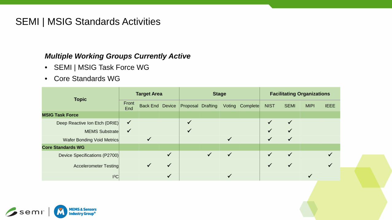
SEMI | MSIG Standards Activities
Multiple Working Groups Currently Active• SEMI | MSIG Task Force WG• Core Standards WG
TopicTarget Area Stage Facilitating Organizations
Front End Back End Device Proposal Drafting Voting Complete NIST SEMI MIPI IEEE
MSIG Task ForceDeep Reactive Ion Etch (DRIE)
MEMS Substrate
Wafer Bonding Void Metrics Core Standards WG
Device Specifications (P2700)
Accelerometer Testing
I3C

SEMI | MSIG Annual Events
JANUARY 9-12, 2018 • LAS VEGAS, NV
MARCH 2017 • SHANGHAI CHINA
MAY 2017 • STANFORD UNIVERSITY
JUNE 26-29, 2017 • SAN JOSE, CA
NOVEMBER 1-2, 2017 • NAPA, CA
SEPT 13, 2017 • TAIPEI TAIWAN JULY 11-13, 2017 • SAN FRANCISCO, CA
SEPTEMBER 20-22, 2017 • GRENOBLE FRANCE 10-11 April | Tokyo
1 June | Seoul
And FlexTech Events

North America Chapter MEMS/NEMS Global Technical CommitteeMicro/Nano Electromechanical SystemsOverviewJune 2017James Amano, SEMI Standards

SEMI Standards Overview
• Established in 1973
• 970+ published Standards & Safety Guidelines
• 5,000+ volunteer experts
• 1,800+ companies
• 21 global technical committees
• Experts from the semiconductor, PV, LED, MEMS & Display industries
• International presence
– United States | Japan | Europe | Taiwan | Korea | China
Exchange ideas and develop globally-accepted technical Standards
10

Critical Role of Standardization
Focus on critical performance variables
More resources for R&D
Faster deliveries
Productive spare parts inventoriesMultiple suppliers reduce costs
Multiple suppliers improve quality
Faster supplier response
Shorter time to market
Customer Supplier
SEMI Standards Reduce Manufacturing Complexity,Allowing Companies to Focus on Innovation
SEMI®International
Standards
11

High-Profile SEMI Standards
• Wafer Dimensions (M1)• Factory efficiency/equipment reliability (E10, E79)• Equipment Interface
– SEMI Equipment Communication Standards (SECS) / Generic Equipment Model (GEM / GEM300)– Hardware/Automated Material Handling Systems (300 mm, 450 mm)
• Environmental, Health and Safety– Safety for Semiconductor (S2), Ergonomic (S8), Energy conservation (S23)
12
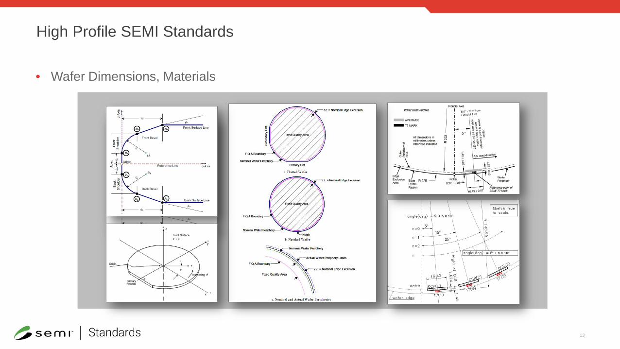
High Profile SEMI Standards
• Wafer Dimensions, Materials
13

High Profile SEMI Standards
• Factory Automation– Equipment Interface Software (SECS/GEM/EDA)– Efficiency, equipment reliability, and availability
14

High Profile SEMI Standards
• Factory Automation– Hardware, AMHS (300 mm, 450 mm)
15

High Profile SEMI Standards
• Environmental, Health and Safety (EHS)
16
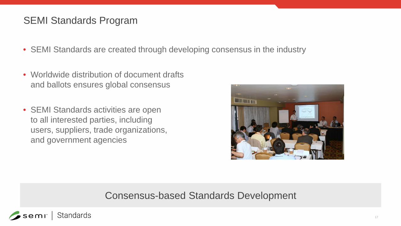
SEMI Standards Program
• SEMI Standards are created through developing consensus in the industry
• Worldwide distribution of document drafts and ballots ensures global consensus
• SEMI Standards activities are open to all interested parties, including users, suppliers, trade organizations, and government agencies
Consensus-based Standards Development
17

SEMI Standards Technical Committees
Assembly & PackagingAutomated Test EquipmentAutomation TechnologyCompound Semiconductor MaterialsEnvironmental Health & SafetyFacilitiesFPD Materials & ComponentsFPD MetrologyGasesHigh-Brightness LEDInformation & Control
Liquid ChemicalsMEMS / NEMSMetricsMicropatterningPhotovoltaicPhotovoltaic MaterialsPhysical Interfaces & CarriersSilicon WaferTraceability3DS-IC
Join SEMI Standardswww.semi.org/en/standardsmembership
18
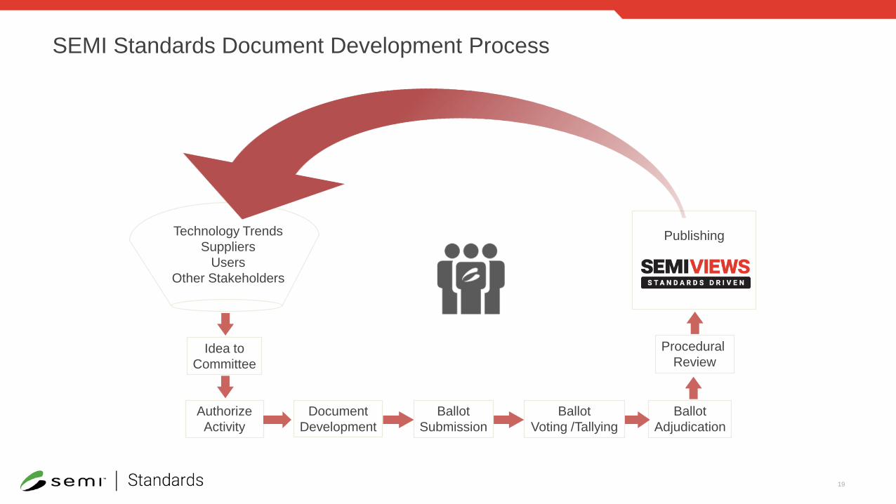
SEMI Standards Document Development Process
Technology TrendsSuppliers
UsersOther Stakeholders
AuthorizeActivity
DocumentDevelopment
Idea toCommittee
BallotVoting /Tallying
Publishing
BallotAdjudication
Procedural Review
BallotSubmission
19

North America Chapter MEMS/NEMS Global Technical CommitteeMicro/Nano Electromechanical Systems
Activities & OverviewApril 2017

MEMS/NEMSCurrent Committee Structure
North America MEMS / NEMS
Technical Committee Chapter
MEMS Packaging TF(Inactive)
MEMS Wafer Bond TF(Inactive)
MEMS Microfluidics TF
MEMS International Terminology TF
(Inactive)
MEMS Material Characterization TF
MEMS Reliability TF(Inactive)
MEMS Substrate TF
21
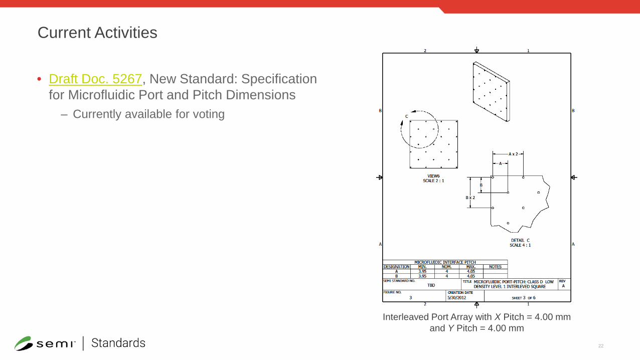
Current Activities
• Draft Doc. 5267, New Standard: Specification for Microfluidic Port and Pitch Dimensions
– Currently available for voting
Interleaved Port Array with X Pitch = 4.00 mm and Y Pitch = 4.00 mm
22

Current Activities
• SNARF Doc. 6007, New Standard: Specification for a Test Pattern for Deep Reactive Ion Etching (DRIE) Process Characterization
– Draft Doc work in-progress with SEMI | MSIG Task Force– To participate in this activity, contact Rich Allen/NIST ([email protected])
• SNARF Doc. 6018, New Standard: Specification for Silicon Substrates used in fabrication of MEMS Devices
– Draft Doc work in-progress, initial proposal from SEMI | MSIG Task Force– To participate in this activity, contact Rich Allen/NIST ([email protected]) and Chris
Moore/Frontier Semiconductor ([email protected])
23

Current Activities
• Draft Doc. 5822A, New Standard: Specification for Reference Material for Bonded Wafer Stack Void Metrology
– Currently available for voting
Layout of the Artificial Voids of Different Sizes and Densities in a Die-Sized Array
24

MEMS Standards Developed
• MS1 – Guide to Specifying Wafer-Wafer Bonding Alignment Targets• MS2 – Test Method for Step-Height Measurements of Thin Films• MS3 – Terminology for MEMS Technology• MS4 – Test Method for Young's Modulus Measurements of Thin, Reflecting Films Based on
the Frequency of Beams in Resonance• MS5 – Test Method for Wafer Bond Strength Measurements Using Micro-Chevron Test
Structures• MS6 – Guide for Design and Materials for Interfacing Microfluidic Systems• MS7 – Specification for Microfluidic Interfaces to Electronic Device Packages• MS8 – Guide to Evaluating Hermeticity of MEMS Packages• MS9 – Specification for High Density Permanent Connections Between Microfluidic Devices• MS10 – Test Method to Measure Fluid Permeation Through MEMS Packaging Materials
25

SEMI MS1Guide to Specifying Wafer-Wafer Bonding Alignment Targets
• This Guide provides a framework for specifying the dimensions, location, quantity and characteristics of alignment targets that are placed on each wafer of a pair of wafers. Such targets are used to align two patterned wafers prior to an operation that bonds them together.
Published Standards [1/10]
26

SEMI MS2Test Method for Step Height Measurements of Thin Films
• This Test Method enables the determination of step height measurements of thin films. Step height measurements can be used to determine thin film thickness values. Thickness measurements are an aid in the design and fabrication of MEMS devices and can be used to obtain thin film material parameters, such as Young’s modulus.
Published Standards [2/10]
27

Published Standards [3/10]
SEMI MS3Terminology for MEMS Technology
To promote common understanding and clear communication among suppliers, customers, and others in the field, these terms should be defined.
This Terminology document covers definitions of terms used in MEMS technology, especially in those areas of greatest interest to the SEMI community.
28

SEMI MS4Test Method for Young's Modulus Measurements of Thin, Reflecting Films Based on the Frequency of Beams in Resonance
• This Test Method covers a procedure for measuring Young’s modulus in thin films. • It applies only to films, such as found in MEMS materials that can be imaged using a noncontact optical vibrometer, stroboscopic interferometer or comparable instrument that is capable of obtaining the resonance frequency of a beam oscillating out-of-plane.
Published Standards [4/10]
29

SEMI MS5Test Method for Wafer Bond Strength Measurements Using Micro-Chevron Test Structures
• This Test Method allows determination of the bond-interface strength, using micro-chevron test structures, of bonded wafer materials.
• The bond-interface strength is expressed in units of energy per unit area and is technically the critical wafer bond toughness.
Published Standards [5/10]
30

SEMI MS6Guide for Design and Materials for Interfacing Microfluidic Systems
• This Document provides guidelines for general fluidic interface design and materials selection that can reduce redundant engineering effort and lead to improved design, manufacturability, and operation.
Published Standards [6/10]
31

SEMI MS7Specification for Microfluidic Interfaces to Electronic Device Packages
• This Document defines an industry-standard for fluidic interfaces with electronic devices. • The specification describes the connection attributes and specifies the interface dimensions required to design and build devices and systems that are compliant with this standard. • The goal is to enable devices from different vendors to interconnect via an open architecture.
Published Standards [7/10]
32
Published Standards [8/10]
SEMI MS8Guide to Evaluating Hermeticity of MEMS Packages
This Document is intended to provide an overview of hermetic packaging with emphasis on the evaluation of hermeticity of the smaller internal volumes typical of MEMS.
Hermeticity is critical to MEMS device functionality. In other cases, hermeticity is primarily important to reliability of MEMS devices, similarly to integrated circuits.
33

Published Standards [9/10]
SEMI MS9Specification for High Density Permanent Connections Between Microfluidic DevicesThis Standard provides specification for interconnection dimensions and performance requirements for permanent microfluidic interfaces. It also provides guidance for interface design. This will help to enable low cost and high volume manufacturing of products having high density permanent interfaces between plastic tube adapters, plastic microfluidic cartridges, and electrofluidic devices.
34

SEMI MS10Test Method to Measure Fluid Permeation Through MEMS Packaging Materials
• This Standard is directed towards defining a common method of measurement of permeation through technical films that are used in sealing hermetic MEMS packages.
• Areas to be addressed include materials and equipment for producing and evaluating hermetic seals; methods for detection and measurement of leakage; and considerations and recommendations on the evaluation of hermeticity.
Published Standards [10/10]
35

Upcoming MEMS / NEMS Meetings
In conjunction with SEMICON West, the North America Standards meetings will be held July 10-13, 2017.
MEMS/NEMS Committee and Task ForceTentative Schedule:Thursday, July 13• 13:00-13:30 Microfluidics (TF)• 13:30-15:30 Joint MSIG, MEMS Substrate and Material Characterization (TF)• 15:30-17:30 MEMS / NEMS (C)
For more information and to register for SEMICON West meetings: https://www.xpressreg.net/register/semi0717/start.asp?sc=STAN2017
36

Thank you!
For more information regarding MEMS/NEMS North America activities, please contact:
Laura [email protected]
For more information regarding SEMI | MSIGPlease contact:Andy Knopes
37

Q & A• Please type your questions into the Q&A box on the GoToWebinar Control Panel• Any question not addressed will be responded to directly
Thank you for attending!
38