sematech defect printability studies - extreme ultraviolet
TRANSCRIPT

Accelerating the next technology revolution
Copyright ©2012
SEMATECH, Inc. SEMATECH, and the SEMATECH logo are registered servicemarks of SEMATECH, Inc. International SEMATECH Manufacturing Initiative, ISMI, Advanced Materials Research Center
and AMRC are servicemarks of SEMATECH, Inc. All other servicemarks and trademarks are the property of their respective owners.
SEMATECH Defect Printability Studies
Il Yong Jang 1, Jenah Harris-Jones 1, Ranganath Teki 1,
Vibhu Jindal 1, Frank Goodwin 1
Masaki Satake 2, Ying Li 2, Danping Peng 2
Sungmin Huh3, Seong-Sue Kim3
1 SEMATECH 2 Luminescent Technologies 3 Samsung Electrinics

Outline
• Introduction
• Experimental procedure and conditions
• Experimental results – Multilayer Geometry
– CD error comparison
• Summary
2 2013 SPIE Advanced Lithography

Major show stopper
3
Since last 5 years, mask yield and defect inspection infra. has been the major show stopper.
Defect levels of EUV mask blanks require further improvement
2013 SPIE Advanced Lithography
Ref.) International EUVL Symposium Program Steering Committee

Recent report
22nm HP node is likely to be the real gateway for EUVL.
Defects of 23nm SEVD start to be printed at the 22nm HP node, however it is not easy to predict the real printability just with SEVD.
It is very important to know the printability of native defects having various dimension to understand phase defect printability.
Simulation work is very important for studying the defect printability.
SEMATECH had begun to study the printability of native defect using simulation and actinic exposure.
4 2013 SPIE Advanced Lithography

Experimental procedure
5
① Substrate Insp.& marking
② AFM analysis
⑥Absorber patterning
2013 SPIE Advanced Lithography
⑦ Wafer Exposure
③ ML deposition ④ AFM analysis
⑤ Absorber deposition
⑧ Analysis
*Images courtesy of www.tel.com, www.veeco.com

Absorber deposition at SEMATECH
6
Absorber deposition with SEMATECH’s IBD chamber
– Optical properties (n=0.9472, k=0.0304, measured@ CXRO, LBNL)
– Thickness : 59nm (3nm ARC + 56nm TaN)
Roughness, stress, chemical durability and defectivity of the absorber
film need to be verified as well.
n&k [email protected] TEM image
2013 SPIE Advanced Lithography

Absorber patterning
7
Absorber patterning at Samsung mask Shop
– Patterning with high-end EBW tool and EUV mask etcher
– Modified etch chemistry due to 1.5 times slower ER than commercial absorber
– Acquired excellent pattern quality and critical dimension SEM
2.8nm LWR
88degs
MTT:1.9nm
88nm 108nm 128nm
AFM
2013 SPIE Advanced Lithography
8
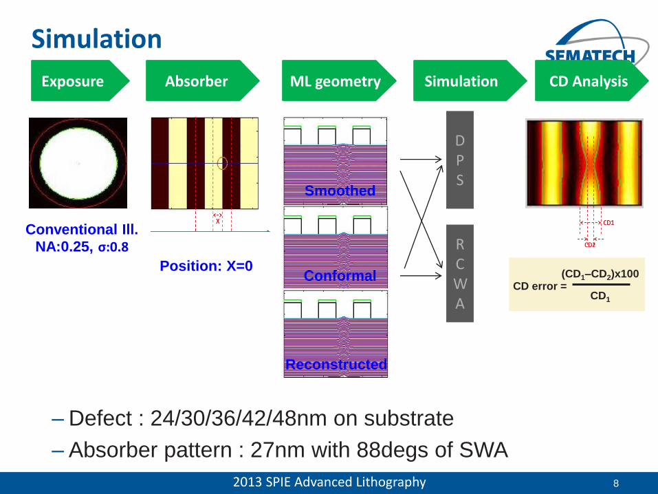
Simulation
– Defect : 24/30/36/42/48nm on substrate
– Absorber pattern : 27nm with 88degs of SWA
2013 SPIE Advanced Lithography
Exposure ML geometry CD Analysis
CD1
(CD1–CD2)x100 CD error =
Absorber Simulation
D P S
RCWA
Conventional Ill.
NA:0.25, σ:0.8
Conformal
Smoothed
Reconstructed
Position: X=0

9
ML Geometry
2013 SPIE Advanced Lithography
ML growth is dependent on the process and
configuration of H/W of ML deposition.
Defect shape changes the ML geometry
No universal ML growth model could give
versatility in defect printability simulation
It is very important to select the optimum ML
geometry to increase simulation accuracy
Used the AFM data measured from substrate
and surface of ML to make a new ML geometry.

10
Smoothed Geometry (for 35nm defect)
2013 SPIE Advanced Lithography
ML pairs ↑ → Defect dimension ↑
Good for any type of defect ?
35nm
Smoothed ML Geometry

11
Conformal Geometry
2013 SPIE Advanced Lithography
Which model should we use for simulation ?
Need to find out the optimum ML geometry for each defect
75nm
Conformal ML Geometry

12
Normalized Dimension
2013 SPIE Advanced Lithography
Surface
β
Substrate
α
Normalized dimension : Surf. dimension β / Sub. dimension α
Measured and got the all normalized dimension from 24nm,
30nm, 36nm, 42nm and 48nm defects

13
Fitting ML geometry
2013 SPIE Advanced Lithography
14
Reconstructed ML geometry
2013 SPIE Advanced Lithography
Defined each defect’s
dimension based on the
fitting curve.
Created “Reconstructed
ML geometry”
Compared the CD error
simulated by three types of
ML geometry.
(Conformal vs Smoothed
vs Reconstructed ML)

15
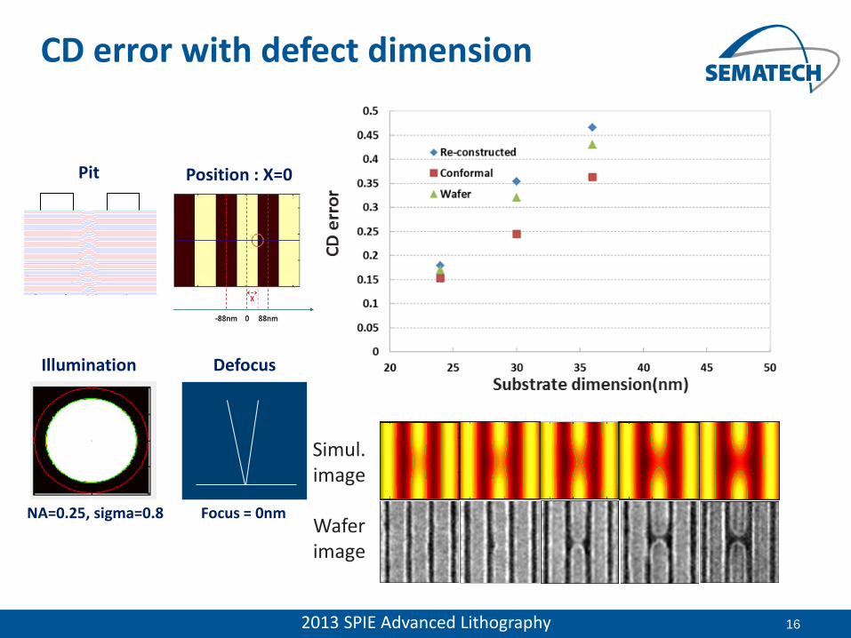
CD error with defect dimension
2013 SPIE Advanced Lithography
Simul. image
Wafer image
Position : X=0
NA=0.25, sigma=0.8
0 100 200 300 400 500 6000
50
100
150
200
250
300
350
X Mask Distance (nm)
Z M
ask H
eig
ht
(nm
)
EUV Mask Geometry Cutline Through Center of DefectBump
Illumination Defocus
Focus = 0nm
16
CD error with defect dimension
2013 SPIE Advanced Lithography
Simul. image
Wafer image
Position : X=0
NA=0.25, sigma=0.8
Pit
Illumination Defocus
Focus = 0nm
0 100 200 300 400 500 6000
50
100
150
200
250
300
350
X Mask Distance (nm)
Z M
ask H
eig
ht
(nm
)
EUV Mask Geometry Cutline Through Center of Defect

CD error with defocus
2013 SPIE Advanced Lithography
Simul. image
Wafer image
Position : X=0
NA=0.25, sigma=0.8
0 100 200 300 400 500 6000
50
100
150
200
250
300
350
X Mask Distance (nm)
Z M
ask H
eig
ht
(nm
)
EUV Mask Geometry Cutline Through Center of DefectBump
Illumination Defect dim.
24nm

CD error with defocus
2013 SPIE Advanced Lithography
Simul. image
Wafer image
Position : X=0
NA=0.25, sigma=0.8
Pit
Illumination Defect dim.
24nm
0 100 200 300 400 500 6000
50
100
150
200
250
300
350
X Mask Distance (nm)
Z M
ask H
eig
ht
(nm
)
EUV Mask Geometry Cutline Through Center of Defect

DPS performance
2013 SPIE Advanced Lithography
CD error from DPS, RCWA and wafer are within 2% range
DPS S/W developed by Luminescent Technologies shows good
simulation accuracy while taking less calculation time than that of
RCWA simulation.

Summary
2013 SPIE Advanced Lithography
Analyzed defect dimensions measured on the
substrate and the ML surface and found correlation
between defect dimension and ML geometry
The reconstructed ML geometry predicts the CD error
better than conventional conformal ML geometry.
24nm bump and pit defects on substrate occurs 7.6%
and 17% of wafer CD error showing that the Teron can
detect the most of defects which could be printed on
wafer for 27nmHP node L&S pattern.
DPS shows good accuracy and faster calculation time
than RCWA simulator.

Acknowledgements
2013 SPIE Advanced Lithography
. Dr. Tsukasa Abe and Naoya Hayashi, DNP for discussing mask manufacturing . Dr. Eric Gullikson from LBNL for providing metrology to measure the optical properties of SEMATECH’s absorber . Gregg Inderhees from KLA-Tencor for providing blank inspection . Dr. Tae-Geun Kim and Dr. Sang-Hyun Kim from Samsung for supporting the defect analysis for this study.