school of engineering science simon fraser university...
TRANSCRIPT

Biomedical Embedded Systems Technology School of Engineering Science
Simon Fraser University Burnaby, BC
March 8, 2010 Dr. Andrew Rawicz School of Engineering Science Simon Fraser University Burnaby, BC V5A 1S6 Re: ENSC 440 Design Specifications for Biomedical Monitoring System Dear Dr. Rawicz: Please see attached for Design Specifications for Biomedical Monitoring System. Our product is a data acquisition system to monitor patients’ cardiovascular health. The monitoring can be done wirelessly or through a USB cable. The document provides the detailed design requirements to satisfy our system’s functional specification. The overall system design, system hardware, software, and user interface design specifications are outlined in the document. Biomedical Embedded Systems Technology (BEST) is a group of innovative engineering students from diverse backgrounds. The team consists of Sam Seyfollahi and Alireza Rahbar (Electronics Engineers), Farzad Abasi (Computer Engineer), Parna Niksirat (Systems Engineer), and Shaghayegh Hosseinpour (Biomedical Engineer). For any further information please feel free to contact me. Yours truly,
TÄ|Üxét et{utÜ Alireza Rahbar President and CEO, BEST Phone: (604) 339-4715 Email: [email protected]
Enclosure: Design Specification for a Biomedical Monitoring System
Biomedical Embedded Systems Technology School of Engineering Science
Simon Fraser University Burnaby, BC
Design Specifications for: Biomedical Monitoring System
Project Team: Alireza Rahbar Farzad Abasi Parna Niksirat Shaghayegh Hosseinpour Sam Seyfollahi
Contact Person: Sam Seyfollahi [email protected]
Submitted to: Dr. Andrew Rawicz – ENSC 440
Mr. Steve Whitmore – ENSC 305 School of Engineering Science
Simon Fraser University
Due date: March 8, 2010 Revision: 1.0
Biomedical Embedded Systems Technology School of Engineering Science
Simon Fraser University Burnaby, BC
i
Executive Summary Cardiovascular diseases (CVDs) are the number one cause of death worldwide [1]. To assist doctors in the early detection of CDVs, Biomedical Embedded Systems Technology (BEST) is developing an advanced heart monitoring system named the Biomedical Monitoring System (BMS). This device is a portable, real time data acquisition system that is capable of acquiring the electrocardiograph, heart rate, and body temperature of a patient. This information can provide doctors key information which can aide in the diagnosis of underlining heart conditions. The statistics gathered by BMS would have traditionally required days of hospital observations or the use of expensive and uncomfortable equipment. BMS will provide accurate results while maintaining the comfort of the patient.
The design specification provides detailed information about the requirements of designing a prototype BMS unit. These specifications contain details of both the functional and nonfunctional design requirements needed to produce the prototype. The document is organized into these major sections:
Hardware specification:
This section outlines the details of the hardware components of the BMS. This includes the microcontroller module, electrocardiograph (ECG) sensors, temperature sensors, flash memory storage, wireless module, Universal Serial Bus (USB) module and physical design of the BMS. Using these specifications, BEST team members will be able to design and produce a working BMS prototype unit.
Software specification:
This section includes the software specifications of the BMS including firmware, drivers, data acquisition functionality and the Graphical User Interface (GUI). Using these specifications, BEST team members will be able to design the software required to for overall BMS functionality.
Other specifications:
This section includes environmental considerations and risk analysis. These important factors need to be carefully considered in the design and development of the BMS prototype to ensure future success.

Biomedical Embedded Systems Technology School of Engineering Science
Simon Fraser University Burnaby, BC
ii
Table of Contents Executive Summary........................................................................................................................................ i Table of Contents............................................................................................................................................ ii List of Figures................................................................................................................................................. iii Glossary............................................................................................................................................................ iii 1. Introduction ................................................................................................................................................ 1
1.1. Scope…...........................................................................................................................................1 1.2. Intended Audience........................................................................................................................ 1
2. System Overview........................................................................................................................................ 2 3.Hardware Design........................................................................................................................................ 3
3.1. Physical Design..............................................................................................................................3 3.2. Microcontroller..............................................................................................................................4
3.2.1. Boot Loader Support………………..……………………………………………6 3.2.2. Data Logger………..………………..……………………………………………6 3.2.3. Transmission of Data..………..……..……………………………………………7
3.2.4. External Flash Memory..…...………..…………………………………………..9 3.2.5. USB10 Daughter Board……..…………………………………………………..10
3.3. Wireless Connectivity................................................................................................................11 3.4. ECG System Design..................................................................................................................13
3.4.1. ECG Risk Analysis………………..……………………………………………..17 3.5. Temperature Sensor...................................................................................................................17
4. GUI ...............................................................................................................................................................18 5. Environment……………………..........................................................................................................19 6. Conclusion..................................................................................................................................................19 7. References...................................................................................................................................................20

Biomedical Embedded Systems Technology School of Engineering Science
Simon Fraser University Burnaby, BC
iii
List of Figures
Figure 1: Biomedical Monitoring System….……………………………………..…………….…..2 Figure 2: Biomedical Monitoring System Block Diagram……………………………………….....3 Figure 3: WASP Microcontroller… ….………………………………………………………........4 Figure 4: Component layout of the WASP microcontroller ….……………………………………5 Figure 5: Flow box diagram of the system in run time…...………………………………………...6 Figure 6: Flow chart of data logger algorithm…...…….………………………………………........8 Figure 7: Block Diagram ….………….………………………………………………………........9 Figure 8: USB10 daughter board….…..………………………………………………………......10 Figure 9: XBee-Pro XSC module... ….………………………………………………………......12 Figure 10: System Data Flow Diagram in a UART interfaced environment..……….…………......13 Figure 11: Normal ECG Signal……. ….………………………………...……………………......14 Figure 12: ECG System Function Block ….………………………...…...……………………......15 Figure 13: ECG Circuit Diagram….. ….………………………………...……………………......15 Figure 14: Transfer function of band pass filter ….………………………………...……………..16 Figure 15: Example of control panel of GUI……………………………………………………..18 Glossary
• A/D: Analog to Digital
• ADC: Analog to Digital Converter
• CVD: Cardiovascular disease
• ECG: Electrocardiograph
• EEPROM: Electrically Erasable Programmable Read-Only Memory
• IEEE: Institute of Electrical and Electronics Engineers
• GND: Ground
• GUI: Graphical User Interface
• SPI: Serial Peripheral Interface
• SRAM: Static Random Access Memory
• UART: Universal Asynchronous Receiver/Transmitter
• USB: Universal Serial Bus
• WPAN: Wireless Personal Area Network

Biomedical Embedded Systems Technology School of Engineering Science
Simon Fraser University Burnaby, BC
© Copyright 2010, BEST March 2010
1
1. Introduction Biomedical Monitoring System (BMS) is a portable heart monitoring system that is used for screening and diagnosis of heart diseases. This system is easy and convenient to use in both the house or fitness centre and can be used for remote real time monitoring. The patient either can be monitored remotely or the data acquired by the system can be transferred through the use of USB cable at a later time. The BMS shows the length of time required for an electrical impulse to travel through the heart. To predict feature heart failures, by collecting data and generating respective graph, BMS makes it easier to monitor the heart. The functional requirements of the BMS, as proposed by Biomedical Embedded System Technology (BEST), are outlined in the following functional specification.
1.1. Scope The scope of this document is to outline all the design details of the BMS in the current development stage. This document addresses the high level design and operation of the BMS. The specified software design methodology, along with the graphical description for the each part is also included in this document. The detailed part arrangement including firmware, sensors, wireless, and the microcontroller is also outlined in this document. The test plan is included at the end of the design specification and will be carefully followed throughout the course of the project.
1.2. Intended Audience The design specification document is intended for use by the design engineers in BEST. The engineers in this team shall refer to this document to ensure that all the design requirements are met in the ongoing development stage. To achieve the best result all the design guidelines described in this document should be followed carefully. Marketing personnel shall use this document to assess the product position in the market and managers will gauge the project’s progress based on these specifications.

Biomedical Embedded Systems Technology School of Engineering Science
Simon Fraser University Burnaby, BC
© Copyright 2010, BEST March 2010
2
2. System Overview The purpose of this project is to make it easier for doctors to monitor patients' heart without making them to travel long distances to do the testing. BEST believes this device can prevent heart attacks caused by undetected heart problems. BMS monitors the heart beat in real time and the data can be transferred to patient or doctor’s cell phone. The heart signal will be captured via ECG sensors; noise reduction will take place, followed by signal amplification (see Figure 2). The amplified signal will be digitized via a micro-controller, and it will be processed to give the resulting graph and data to the output interface. The output interface is a graphic interface that makes it convenient for the user to view the resulting graphs and insert the desire settings for the micro-controller. System overview of BMS is presented in figure 1.
Figure 1: Biomedical Monitoring System

Biomedical Embedded Systems Technology School of Engineering Science
Simon Fraser University Burnaby, BC
© Copyright 2010, BEST March 2010
3
Figure 2: Biomedical Monitoring System Block Diagram
3. Hardware Design
3.1. Physical design For the physical design of BMS, we needed something that would be light and comfortable to wear for extended periods of time. For the purposes of prototyping, we have decided to design a simple poly (methyl methacrylate) (Plexiglas) case. This helps keep the components safe from debris and moisture while keeping the packaging lightweight. The case will then be encased in a silicone outer shell to make the device soft and comfortable for the user to wear. The outer silicon shell will also include a belt loop which will allow the unit to be securely mounted around the user’s waist.
Also note: since the BMS creates a negligible amount of heat when in use, it will not require any additional cooling measures. This means that the unit can be sealed and self contained, which will protect the circuitry from the elements.
For the final production unit, we will use a professional plastic injection molding manufacturing process to create a more compact and ascetically pleasing look.

Biomedical Embedded Systems Technology School of Engineering Science
Simon Fraser University Burnaby, BC
© Copyright 2010, BEST March 2010
4
3.2. Microcontroller We have decided to use a SOC Robotics Wasp microcontroller (with an Atmel ATmega644 processor) that will act as the processing unit for data acquisition. Figure 3 shows a picture of the WASP microcontroller. In addition, the microcontroller will also prepare data for transmission through the wireless module or USB cable to a computer for analysis. Some of the characteristics of this microcontroller are as follow [1]:
• 8bit RISC AVR Processor (ATmega644) • 8MHz External crystal oscillator • 8 digital to analog (ADD) 10 bit channels • 15 Digital Input/Output • 64K Internal Program Flash • 2K Internal EEPROM • 4K Internal SRAM • 64 MB External Serial Flash: Suitable to save acquired data from sensor for 24
hours • ISP Programming Port • Machine pins on J1, J2, J3 to enable stacking • Extremely Small form factor (1.47x1.15 in) • 1.8-5VDC @ 12ma Power input: Low power consumption makes the
microcontroller ideal for our application.
Figure 3: WASP Microcontroller
Biomedical Embedded Systems Technology School of Engineering Science
Simon Fraser University Burnaby, BC
© Copyright 2010, BEST March 2010
5
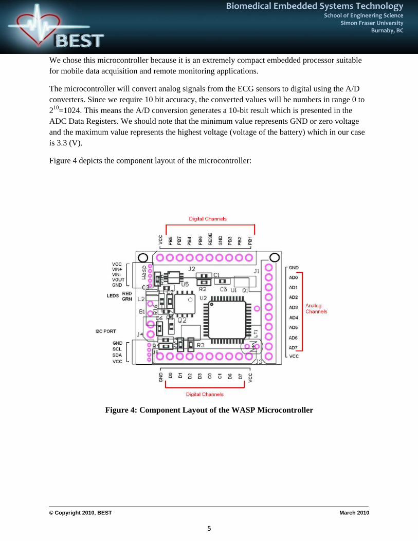
We chose this microcontroller because it is an extremely compact embedded processor suitable for mobile data acquisition and remote monitoring applications.
The microcontroller will convert analog signals from the ECG sensors to digital using the A/D converters. Since we require 10 bit accuracy, the converted values will be numbers in range 0 to 210=1024. This means the A/D conversion generates a 10-bit result which is presented in the ADC Data Registers. We should note that the minimum value represents GND or zero voltage and the maximum value represents the highest voltage (voltage of the battery) which in our case is 3.3 (V).
Figure 4 depicts the component layout of the microcontroller:
Figure 4: Component Layout of the WASP Microcontroller

Biomedical Embedded Systems Technology School of Engineering Science
Simon Fraser University Burnaby, BC
© Copyright 2010, BEST March 2010
6
3.2.1. Boot Loader Support: AVR Atmega644 Boot Loader Support provides a real read-while-write self-programming mechanism for downloading and uploading program code to and from the microcontroller. The boot loader program can use any available data interface and associated protocol to write (program) the code into the flash memory, or read the code from the program memory[2].
The importance of the boot loader is that microcontroller will remember its previous settings. That means every time the microcontroller is powered up, the boot loader will look into the flash memory and loads the saved settings of the microcontroller.
Figure 5 is the flow box diagram of the system in run time. User will switch on the microcontroller using a switch outside of the enclosure. After the system is activated, the boot loader will run the program then the system will load any pre-defined settings that have been saved on EEPROM. These settings, such as sample rate and starting condition, will be saved on
EEPROM after each time the user uploads them to the microcontroller from the GUI. In case no settings were found, microcontroller will use predefined settings for data acquisition.
Figure 5: Flow box diagram of the system in run time
3.2.2. Data Logger: In order to start reading the sensor values, we have two different options:
• Start button on the GUI is pressed and then start command is transmitted to the device through USB or wireless
• A push button switch is pushed and a digital pin is pulled high (that is one of the digital pins turns 1 from 0). We picked digital pin number 0 “D0” to attach the switch to. See Figure 4 for pin layout.
Power up Loading/ assigning settings
Wait for start command
Start data logging
Biomedical Embedded Systems Technology School of Engineering Science
Simon Fraser University Burnaby, BC
© Copyright 2010, BEST March 2010
7
After starting condition is met, the microcontroller will start running the data logger algorithm. Figure 6 shows the flow chart of this algorithm.
3.2.3. Transmission of Data: Collected sensor data needs to be transmitted to a computer for displaying in the GUI and analysis. This can be done in real-time, or data can be saved on a flash memory and later transferred to the computer.
Transferring in real-time can be done through a wireless device as well as USB interface. Based on the defined settings of the user, as discussed earlier, the microcontroller will transmit the data either in real time or store it onto the on-board flash memory. The default method for transmission of data is through USB interface.
If the user decides to use the on board memory for storing, data can be retrieved though USB interface to the computer. In this case, GUI will send a command for retrieving data to the microcontroller indicating that it is waiting to collect the data. The microcontroller will then start transmitting the data through USB to the computer where they will be saved as a “*.dat” file.

Biomedical Embedded Systems Technology School of Engineering Science
Simon Fraser University Burnaby, BC
© Copyright 2010, BEST March 2010
8
Figure 6: flow chart of data logger algorithm.
Start
Initialize settings
Starting condition?
ADC done? Update Buffer
On‐board Storage?
Store data on flash memory
Wireless transmission
USB transmission
Send data through wireless module
Send data through USB
YES
YES
YES
YES
YES
Biomedical Embedded Systems Technology School of Engineering Science
Simon Fraser University Burnaby, BC
© Copyright 2010, BEST March 2010
9
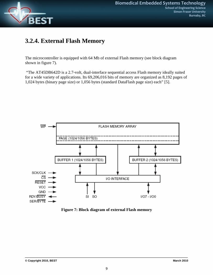
3.2.4. External Flash Memory
The microcontroller is equipped with 64 Mb of external Flash memory (see block diagram shown in figure 7). “The AT45DB642D is a 2.7-volt, dual-interface sequential access Flash memory ideally suited for a wide variety of applications. Its 69,206,016 bits of memory are organized as 8,192 pages of 1,024 bytes (binary page size) or 1,056 bytes (standard DataFlash page size) each” [5].
Figure 7: Block diagram of external Flash memory

Biomedical Embedded Systems Technology School of Engineering Science
Simon Fraser University Burnaby, BC
© Copyright 2010, BEST March 2010
10
Below is a summary of the features of the external flash memory [5]:
• Single 2.7V - 3.6V Supply • Dual-interface Architecture • RapidS Serial Interface: 66 MHz Maximum Clock Frequency • SPI Compatible Modes 0 and 3 • Rapid8 8-bit Interface: 50 MHz Maximum Clock Frequency • User Configurable Page Size • Two SRAM Data Buffers (1024/1056 Bytes) • Allows Receiving of Data while Reprogramming the Flash Array • Continuous Read Capability through Entire Array • Low-power Dissipation • 64-byte User Programmable Space • Data Retention – 20 Years • Industrial: -40°C to +85°C
3.2.5.USB10 Daughter Board Unfortunately WASP microcontroller does not have any USB output. To be able to communicate with USB we are using a daughter board USB10 that mounts on the WASP microcontroller. The lower board (see figure 8) is a USB peripheral based on the Atmel AVR AT90USB162 embedded processor which will provide USB 2.0 connectivity for our device.
Figure 8: USB10 daoughter board

Biomedical Embedded Systems Technology School of Engineering Science
Simon Fraser University Burnaby, BC
© Copyright 2010, BEST March 2010
11
The USB10 daughter board has the following features [3]:
• USB 2.0 compatible • AT90USB162 AVR Processor • 16MHz on board crystal (clock set to 8MHz) • SPI Port • 16K Internal Program Flash (4K taken by boot loader) • 512-byte SRAM, 512-byte EEPROM • Debug Wire interface for on-chip-debug • Extremely Small form factor (1.51x1.16 in) • 3.3-5VDC @ 8-25ma Power input (clock dependent)
The board provides a serial communication path between the microcontroller and a PC via USB. After developing the hardware drivers (using C programming language), the USB connection will be one of the options to transfer acquired data from the data acquisition device to PC. The other option (as will be mentioned in part 3.3) will be wireless transferring of data.
3.3. Wireless connectivity Wireless connectivity will bring a greater degree of freedom and mobility to BMS. With the wireless module, our system can monitor users remotely in real time as well as allow for data to be transferred to the host computer. This will allow the user to wear the device while performing physical activities both at the gym and outdoors. Additionally, the system can always fall back to storing information to onboard memory in case of connectivity issues. For wireless connectivity, we have decided to use the ZigBee specification. “ZigBee is a specification for a suite of high level communication protocols using small, low-power digital radios based on the IEEE 802.15.4-2003 standard for wireless personal area networks (WPANs)” [7]. BEST chose to use ZigBee because of the low cost and low power requirement as well as long transmission range required for remote monitoring.
The wireless module we have decided to incorporate into our system is the XBee-PRO® XSC RF transceiver module (see figure 9 [8]).

Biomedical Embedded Systems Technology School of Engineering Science
Simon Fraser University Burnaby, BC
© Copyright 2010, BEST March 2010
12
Figure 9: XBee-Pro XSC module
The characteristics of this module are as follow [8]:
• Power output: 100 mW (20 dBm) • Indoor/Urban range: Up to 1200 ft (370 m) • Outdoor/RF line-of-sight range: up to 15 miles (24 km) • Receiver sensitivity: -106 dBm • RF data rate: 9.6 Kbps • Supply voltage: 3.0 - 3.6VDC • Transmit current: 265 mA • Receive current: 65 mA power-down • Frequency Band: 910 - 918 MHz • Serial Data Interface: 3.3V CMOS UART (5V tolerant inputs) • Size: 0.960 in x 1.087 in (2.438 cm x 2.761 cm) • Weight: 0.10 oz (3 g) w/ U.FL connector
To transmit data wirelessly from the microprocessor to the host computer, we will be using two of these modules. The transmitter module will connect to the BMS microcontroller using the SPI bus and the receiver module will be connected to the computer using a serial UART port. A system data flow diagram is provided below in figure 10 [8].

Biomedical Embedded Systems Technology School of Engineering Science
Simon Fraser University Burnaby, BC
© Copyright 2010, BEST March 2010
13
Figure 10: System Data Flow Diagram in a UART‐interfaced environment
3.4. ECG System Design An electrocardiogram (ECG) is a graphic tracing of the electric current generated by the heart muscle during a heartbeat. The voltages produced represent pressures exerted by the heart muscles in one pumping cycle.
A typical single cardiac waveform of a normal heartbeat is shown below in figure 11:

Biomedical Embedded Systems Technology School of Engineering Science
Simon Fraser University Burnaby, BC
© Copyright 2010, BEST March 2010
14
Figure 11: Normal ECG signal [10]
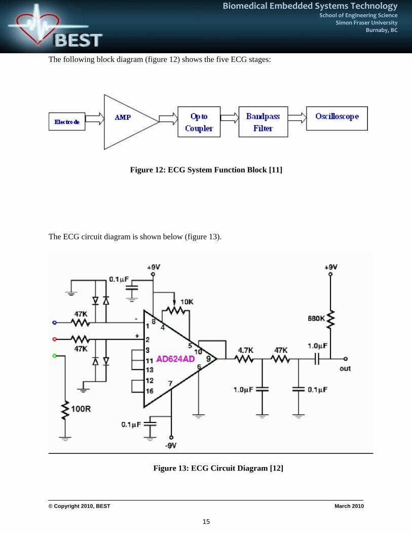
In general the ECG system consists of five stages;
1. The first stage is a transducer (AgCl electrode), which converts ECG signal into electrical voltage. The voltage is in the range of 1 mV - 5 mV.
2. The second stage is an instrumentation amplifier (Analog Device, AD624 ) with high gain (1000) and power supply +9V and -9V.
3. The third stage is the opto-coupler (NEC PS2506) to isolate the In-Amp from the rest of circuits.
4. The fourth stage is a band pass filter of 0.04 Hz to 150 Hz. It is applied by cascading a band pass filter (low-pass filter and a high pass filter).
5. The last stage is a oscilloscope that allows signal voltages to be viewed.
Biomedical Embedded Systems Technology School of Engineering Science
Simon Fraser University Burnaby, BC
© Copyright 2010, BEST March 2010
15
The following block diagram (figure 12) shows the five ECG stages:
Figure 12: ECG System Function Block [11]
The ECG circuit diagram is shown below (figure 13).
Figure 13: ECG Circuit Diagram [12]
Biomedical Embedded Systems Technology School of Engineering Science
Simon Fraser University Burnaby, BC
© Copyright 2010, BEST March 2010
16
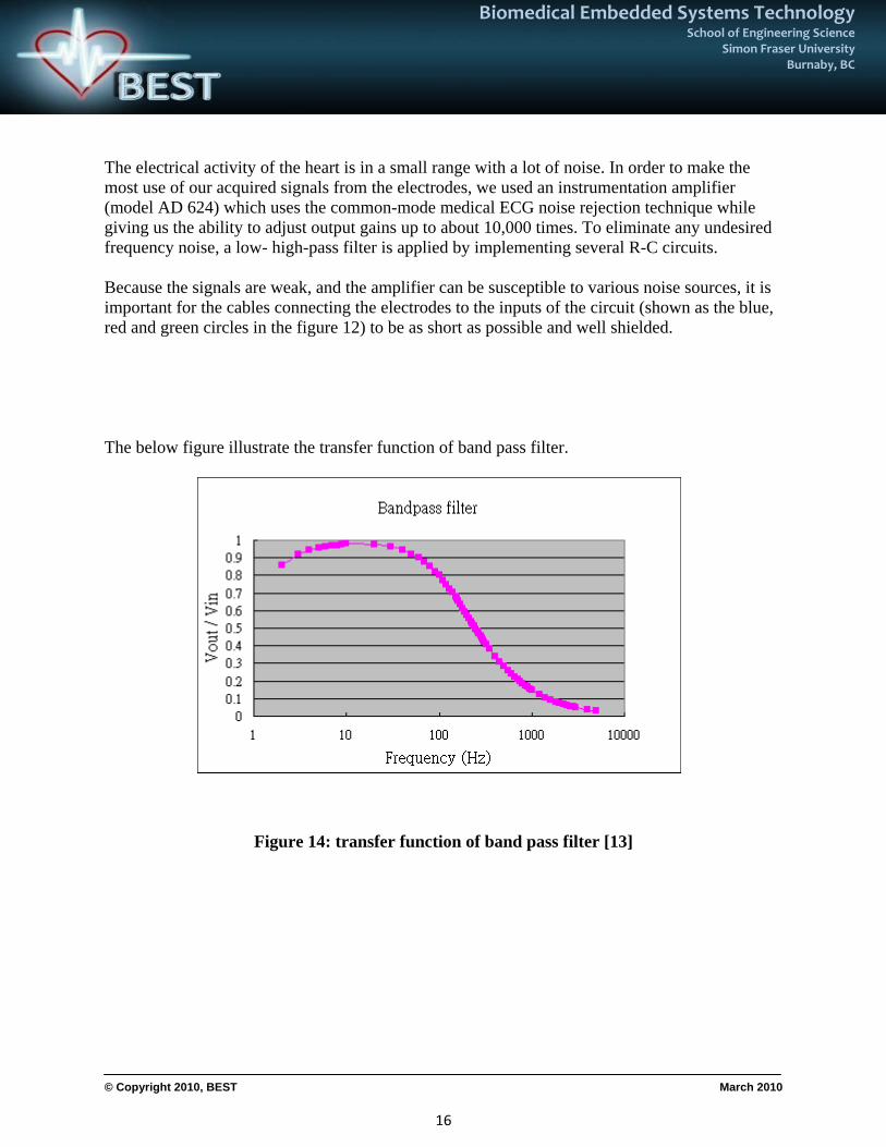
The electrical activity of the heart is in a small range with a lot of noise. In order to make the most use of our acquired signals from the electrodes, we used an instrumentation amplifier (model AD 624) which uses the common-mode medical ECG noise rejection technique while giving us the ability to adjust output gains up to about 10,000 times. To eliminate any undesired frequency noise, a low- high-pass filter is applied by implementing several R-C circuits. Because the signals are weak, and the amplifier can be susceptible to various noise sources, it is important for the cables connecting the electrodes to the inputs of the circuit (shown as the blue, red and green circles in the figure 12) to be as short as possible and well shielded. The below figure illustrate the transfer function of band pass filter.
Figure 14: transfer function of band pass filter [13]
Biomedical Embedded Systems Technology School of Engineering Science
Simon Fraser University Burnaby, BC
© Copyright 2010, BEST March 2010
17
3.4.1. ECG Risk Analysis The voltage output, Vout from the low-high pass filter is fed to the analog-to-digital converter (A/D) integrated in the microcontroller. This converts the analog signal into a digital format. The relevant output of the A/D convertor will be transmitted to the computer via wireless modem for further analysis. Consequently the heart rate will be determined from the heart data every 5-10 seconds. A normal heart rate at rest is approximately within the range of 60-100 beats per minute (bpm). Any figure not falling within this norm is known as arrhythmia. Depending on the age, the theoretical maximum exercise heart rates can reach up to 180 bpm. The easiest and best known method to calculate your maximum heart rate (MHR) is to use the formula MHR = 220 bpm - age The user and medical authorities shall be contacted if any of the following happens:
• The average calculated heart rates vary by more than 15% from each other
• The average calculated heart rate is higher than 75% of the maximal heart rate • The average calculated heart rate is slower than 40 bpm
3.5. Temperature Sensor Patients on extended stays in hospitals often require continuous body temperature monitoring. Skin temperature sensors are mostly used for this purpose. There are circumstances however where this is not possible. Patients with severe burns or sensitive skin cannot have anything taped to their skin. In addition, a more accurate measurement may be required. For these instances a rectal temperature sensor is used.
The AD592 is a two terminal monolithic integrated circuit temperature transducer that provides an output current proportional to absolute temperature. For a wide range of supply voltages the transducer acts as a high impedance temperature dependent current source of 1 uA/K. With a single supply (4 V to 30 V) the AD592 offers 0.5°C temperature measurement accuracy. The voltage output, VOUT, from of the temperature sensor will be fed to the A/D converter integrated in the microcontroller, and converted into a binary format which is sent to the computer for further processing.

Biomedical Embedded Systems Technology School of Engineering Science
Simon Fraser University Burnaby, BC
© Copyright 2010, BEST March 2010
18
4. GUI The GUI is a monitoring interface that displays the data from controller. This interface communicates with microcontroller in real time. It sends data to the microcontroller, receives data from microcontroller and presents data to the user. From the GUI users can define the data transmission rate, the data bit, parity settings and channel settings. The GUI has three tabs each lead the user to a new screen: Real Time Data Logger, Channels, and Display (See Figure 15). The Real Time Data Logger has a control panel to start the real time display mode as well as the ability to save and print the displayed information. Inside the Channel tab the user can set the digital input and the threshold value for the emergency purposes. If the data from the controller exceed a predefined threshold the emergency alert will notify the user that system has detected an unusual case. The User can also specify the channel's property and the resolution of the data coming from each pin inside the Display tab in order to view the desired graph. The GUI can save the data captured in to a text file for future analysis. By clicking on each point in the graph the user can extract specific information about that section of the graph which makes it easier and more convenient for further analysis.
Figure 15: Example of Control Panel of GUI
Biomedical Embedded Systems Technology School of Engineering Science
Simon Fraser University Burnaby, BC
© Copyright 2010, BEST March 2010
19
5. Environment In Canada (and the rest of the world) product companies are being introduced to the Restriction of Hazardous Substances (RoHS) and Waste Electrical and Electronic Equipment (WEEE) standards. At the same time, to protect the environment there is a lead-free restriction when it comes to product manufacturing, recycling and disposal. During the design phase, BEST selected environmentally friendly and recyclable parts that are not hazardous to the environment and meet the RoHS/WEEE standards. In this section the considerations of making BMS environmentally friendly are outlined. For the packaging of the product BEST will use recyclable and lead-free material to help reduce waste. The link to the website that recycles the electronics part in Vancouver is provided at the end of this report in the references. To reduce the battery consumption the product will be equipped with rechargeable battery. Studies show that rechargeable batteries have up to thirty two times less impact on the environment than the disposable batteries. Rechargeable batteries produce less waste for the environment because they can be reused. They also save energy because the energy needed to manufacture a battery is on average fifty times greater than the energy it gives out[14]. By recycling electronics to Electronics Recycling Association, not only do we save the environment, but we also bring back the product to life for donation to people in need and communities.
6. Conclusion The proposed design solution for Biomedical Monitoring Systems (BMS) has been presented in this document. The solutions given in this document are tentative and will be modified accordingly to meet the functional specification. In the test plan, we will ensure that all functionalities of the device are tested and properly working as expected. The final product will benefit not only health care providers, but also professional athletes. Our product will make it easier for athletes to constantly monitor their performance and to help detect early signs of heart failure. This system will be perfectly integrated, simple to use and to install. We are certain that with the special features included in this system, our monitoring and measuring system will stand out among all other competitors
Biomedical Embedded Systems Technology School of Engineering Science
Simon Fraser University Burnaby, BC
© Copyright 2010, BEST March 2010
20
7. References: [1] http://www.soc-machines.com/pdfs/Wasp%20Hardware%20Reference%20Guide.pdf
[2] http://www.atmel.com/dyn/resources/prod_documents/32058S.pdf
[3] http://www.olimex.com/dev/avr-usb-162.html [4] http://www.atmel.com/dyn/Products/product_card.asp?part_id=4097 [5] http://www.atmel.com/dyn/resources/prod_documents/doc3542.pdf
[6] http://www.who.int/mediacentre/factsheets/fs317/en/index.html
[7] ZigBee http://en.wikipedia.org/wiki/ZigBee_specification
[8] Xbee module ftp://ftp1.digi.com/support/documentation/90000938_a.pdf
[9] http://www.era.ca/donations/recycling/vancouver.html [10] http://www.davita-shop.co.uk/ecg-instruments.html [11] http://www.cisl.columbia.edu/kinget_group/student_projects/ECG%20Report/E6001%20ECG %20final%20report.htm
[12] http://www.picotech.com/applications/ecg.html [13]http://www.cisl.columbia.edu/kinget_group/student_projects/ECG%20Report/E6001%20ECG%20final%20report.htm
[14] http://www.iere.org/index.html