school of bio and chemical enginneering department …
TRANSCRIPT

1
SCHOOL OF BIO AND CHEMICAL ENGINNEERING
DEPARTMENT OF BIOMEDICAL ENGINEERING
Unit - I
Evolution of Microprocessor – Architecture – Instruction format – Addressing modes –
Basic timing diagram –Opcode fetch –Memory Read- Memory write- I/O Read-I/O Write-
Interrupts in 8085-Software interrupts- Hardware interrupts- Priorities of Interrupts- 8085
based system design.
.
Fundamentals of Microprocessor and Microcontroller – SEC1323

2
1.1Evolution of Microprocessor:
It can be classified as following types
1.1.1First generation of processor: 4-bit Microprocessor
The first microprocessor was introduced in 1971 by Intel Corp. It was named Intel 4004 as it
was a 4 bit processor. It was a processor on a single chip. It could perform simple arithmetic and
logic operations such as addition, subtraction, Boolean AND & Boolean OR. It had a control unit
capable of performing control functions like fetching an instruction from memory, decoding it,
and generating control pulses to execute it. It was able to operate on 4 bits of data at a time. This
first microprocessor was quite a success in industry. Soon other microprocessors were also
introduced. Intel introduced the enhanced version of 4004, the 4040. Some other 4 bit processors
are International’s PPS4 and Toshiba’s T3472. 1.1.2Second generation of processor: 8-bit Microprocessor
The first 8 bit microprocessor which could perform arithmetic and logic operations on 8 bit
words was introduced in 1973 again by Intel. This was Intel 8008 and was later followed by an
improved version, Intel 8088. Some other 8 bit processors are Zilog-80 and Motorola M6800. 1.1.3 Third generation of processor: 16-bit Microprocessor
The 8-bit processors were followed by 16 bit processors. They are Intel 8086 and 80286.
1.1.4Fourth generation of processor: 32-bit Microprocessor
The 32 bit microprocessors were introduced by several companies but the most popular one is
Intel 80386.
1.1.5Fifth generation of processor: Pentium Series
Instead of 80586, Intel came out with a new processor namely Pentium processor. Its
performance is closer to RISC performance. Pentium was followed by Pentium Pro CPU.
Pentium Pro allows allow multiple CPUs in a single system in order to achieve multiprocessing.
The MMX extension was added to Pentium Pro and the result was Pentium II. The low cost
version of Pentium II is Celeron. The Pentium III provided high performance floating point
operations for certain types of computations by using the SIMD extensions to the instruction set.
These new instructions make the Pentium III faster than high-end RISC CPUs.
Interestingly Pentium IV could not execute code faster than the Pentium III when running at the
same clock frequency. So Pentium IV had to speed up by executing at a much higher clock
frequency.
1.2.Internal Architecture of 8085 Microprocessor:
The functional block diagram or architecture of 8085 Microprocessor is very important as it
gives the complete details about a Microprocessor. Fig1.1 shows the Block diagram of a
Microprocessor.

3
Figure 1.1 8085 Microprocessor Architecture
Diagram
It consists of the following:
Control Unit
Generates signals within µP to carry out the instruction, which has been decoded. In reality
causes certain connections between blocks of the µP to be opened or closed, so that data goes
where it is required, and so that ALU operations occur.
Arithmetic Logic Unit
The ALU performs the actual numerical and logic operation such as ‘add’, ‘subtract’, ‘AND’,
‘OR’, etc. Uses data from memory and from Accumulator to perform arithmetic. Always stores
result of operation in Accumulator.
Registers
The 8085/8080A-programming model includes six registers, one accumulator, and one flag
register. In addition, it has two 16-bit registers: the stack pointer and the program counter. They
are described briefly in Figure 1.2.
The 8085/8080A has six general- purpose registers to store 8-bit data; these are identified as B,
C, D, E, H, and L as shown in the figure. They can be combined as register pairs - BC, DE, and
HL - to perform some 16-bit operations. The programmer can use these registers to store or copy
data into the registers by using data copy instructions.

4
Figure 1.2 8085 Microprocessor Registers set
Accumulator (A):
It is an 8-bit register that is part of the arithmetic/logic unit (ALU).
Used to store 8-bit data and to perform arithmetic and logical operations.
The result of an operation is stored in the accumulator.
Flags:
The ALU includes five flip-flops that are set or reset according to the result of an operation.
The microprocessor uses the flags for testing the data conditions.
They are Zero (Z), Carry (CY), Sign (S), Parity (P), and Auxiliary Carry (AC) flags. The most
commonly used flags are Sign, Zero, and Carry.
The bit position for the flags in flag register is,
Sign Flag (S):
• After execution of any arithmetic and logical operation, if D7 of the result is 1, the
sign flag is set. Otherwise it is reset. D7 is reserved for indicating the sign; the
remaining is the magnitude of number.
• If D7 is 1, the number will be viewed as negative number. If D7 is 0, the
number will be viewed as positive number.
Zero Flag (z):
• If the result of arithmetic and logical operation is zero, then zero flag is set otherwise it is reset.
Auxiliary Carry Flag (AC):
• If D3 generates any carry when doing any arithmetic and logical
operation, this flag is set. Otherwise it is reset.

5
Parity Flag (P):
• If the result of arithmetic and logical operation contains even number of 1's then
this flag will be set and if it is odd number of 1's it will be reset.
Carry Flag (CY):
• If any arithmetic and logical operation result any carry then carry flag is set otherwise it is reset.
Program Counter (PC):
• This 16-bit register sequencing the execution of instructions. It is a memory
pointer. Memory locations have 16-bit addresses, and that is why this is a 16-bit
register.
• The function of the program counter is to point to the memory address of the
next instruction to be executed.
• When an opcode is being fetched, the program counter is incremented by one to
point to the next memory location.
Stack Pointer (SP):
The stack pointer is also a 16-bit register used as a memory pointer. It points to a memory location in R/W memory, called the stack.
The beginning of the stack is defined by loading a 16-bit address in the stack pointer.
Temporary Register:
• It is used to hold the data during the arithmetic and logical operations.
Instruction Register:
• When an instruction is fetched from the memory, it is loaded in the instruction register.
Instruction Decoder:
• It gets the instruction from the instruction register and decodes the
instruction. It identifies the instruction to be performed. Serial I/O Control:
• It has two control signals named SID and SOD for serial data transmission.
Timing and Control unit:
It has three control signals ALE, RD (Active low) and WR (Active low) and three status signals IO/M(Active low), S0 and S1. The control word shown in table .1
ALE is used for provide control signal to synchronize the components of
microprocessor and timing for instruction to perform the operation.
RD (Active low) and WR (Active low) are used to indicate whether the operation is reading
the data from memory or writing the data into memory respectively.IO/M(Active low) is used
to indicate whether the operation is belongs to the memory or peripherals.

6
Table 1: Read/Write data
1.2.1 8085 System Bus
Typical system uses a number of busses, collection of wires, which transmit binary numbers, one
bit per wire. A typical microprocessor communicates with memory and other devices (input and
output) using three busses: Address Bus, Data Bus and Control Bus.
1.2.1.1 Address Bus:
The address bus is a group of 16 lines generally identified as A0 to A15.
The address bus is unidirectional: bits flow in one direction-from the MPU to
peripheral devices.
The MPU uses the address bus to perform the first function: identifying a
peripheral or a memory location.
Figure 1.3 Bus interfaced with Microprocessor
Data Bus:
The data bus is a group of eight lines used for data flow.

7
These lines are bi-directional - data flow in both directions between the MPU and memory and
peripheral devices.
The MPU uses the data bus to perform the second function: transferring binary information.
The eight data lines enable the MPU to manipulate 8-bit data ranging from 00 to FF (28 = 256
numbers).
The largest number that can appear on the data bus is 11111111.
1.2.2 Control Bus:
The control bus carries synchronization signals and providing timing signals.
The MPU generates specific control signals for every operation it performs. These signals
are used to identify a device type with which the MPU wants to communicate.
1.3 8085 Pin details. The diagram shown in Figure 1.4
Figure 1.4 Pin Diagram of 8085 Microprocessor
Properties
Single + 5V Supply
4 Vectored Interrupts (One is Non Maskable) Serial In/Serial Out
Port
Decimal, Binary, and Double Precision Arithmetic Direct
Addressing Capability to 64K bytes of memory
The Intel 8085A is a new generation, complete 8 bit parallel central processing unit (CPU). The
8085A uses a multiplexed data bus. The address is split between the 8bit address bus and the 8bit
data bus.
Pin Description
The following describes the function of each pin:
A6 - A1s (Output 3 State)- Address Bus: The most significant 8 bits of the memory address or the
8 bits of the I/0 address,3 stated during Hold and Halt modes.
AD0 - AD7 (Input/Output 3state) Multiplexed Address/Data Bus; Lower 8 bits of the memory
address (or I/0 address) appear on the bus during the first clock cycle of a machine state. It then
becomes the data bus during the second and third clock cycles. 3 stated during Hold and Halt
modes.

8
ALE (Output)- Address Latch Enable: It occurs during the first clock cycle of a machine state and
enables the address to get latched into the on chip latch of peripherals. The falling edge of ALE is
set to guarantee setup and hold times for the address information. ALE can also be used to strobe
the status information. ALE is never 3stated.
SO, S1 (Output)-Data Bus Status. Encoded status of the bus cycle shown in table .2
Table .2 control word
S1 S0 0 0 HALT
0 1 WRITE
1 0 READ
1 1 FETCH
S1 can be used as an advanced R/W status.
RD (Output 3state)- READ; indicates the selected memory or 1/0 device is to be read and that the
Data Bus is available for the data transfer.
WR (Output 3state)- WRITE; indicates the data on the Data Bus is to be written into the selected
memory or 1/0 location. Data is set up at the trailing edge of WR. 3stated during Hold and Halt
modes.
READY (Input)- If Ready is high during a read or write cycle, it indicates that the memory or
peripheral is ready to send or receive data. If Ready is low, the CPU will wait for Ready to go
high before completing the read or write cycle.
HOLD (Input)- HOLD; indicates that another Master is requesting the use of the Address and
Data Buses. The CPU, upon receiving the Hold request. will relinquish the use of buses as soon
as the completion of the current machine cycle. Internal processing can continue. The processor
can regain the buses only after the Hold is removed. When the Hold is acknowledged, the
Address, Data, RD, WR, and IO/M lines are 3stated.
HLDA (Output)- HOLD ACKNOWLEDGE; indicates that the CPU has received the Hold request
and that it will relinquish the buses in the next clock cycle. HLDA goes low after the Hold
request is removed. The CPU takes the buses one half clock cycle after HLDA goes low.
INTR (Input)- INTERRUPT REQUEST; is used as a general purpose interrupt. It is sampled only
during the next to the last clock cycle of the instruction. If it is active, the Program Counter (PC)
will be inhibited from incrementing and an INTA will be issued. During this cycle a RESTART
or CALL instruction can be inserted to jump to the interrupt service routine. The INTR is enabled
and disabled by software. It is disabled by Reset and immediately after an interrupt is accepted.
INTA (Output)- INTERRUPT ACKNOWLEDGE; is used instead of (and has the same timing as)
RD during the Instruction cycle after an INTR is accepted. It can be used to activate the 8259
Interrupt chip or some other interrupt port.
RST 5.5
RST 6.5 - (Inputs) RST
7.5
RESTART INTERRUPTS; These three inputs have the same timing as I NTR except they cause
an internal RESTART to be automatically inserted.
RST 7.5 Highest Priority
RST 6.5
RST 5.5 Lowest Priority

9
The priority of these interrupts is ordered as shown above. These interrupts have a higher priority
than the INTR.
TRAP (Input)-Trap interrupt is a nonmaskable restart interrupt. It is recognized at the same time
as INTR. It is unaffected by any mask or Interrupt Enable. It has the highest priority of any
interrupt.
RESET IN (Input)- Reset sets the Program Counter to zero and resets the Interrupt Enable and
HLDA flipflops. None of the other flags or registers (except the instruction register) are affected
The CPU is held in the reset condition as long as Reset is applied. RESET OUT (Output)-
Indicates CPlJ is being reset. Can be used as a system RESET. The signal is synchronized to the
processor clock.
X1, X2 (Input)-Crystal or R/C network connections to set the internal clock generator X1 can also
be an external clock input instead of a crystal. The input frequency is divided by 2 to give the
internal operating frequency.
CLK (Output)-Clock Output for use as a system clock when a crystal or R/ C network is used as
an input to the CPU. The period of CLK is twice the X1, X2 input period.
IO/M (Output)-IO/M indicates whether the Read/Write is to memory or l/O Tristated during Hold
and Halt modes.
SID (Input)- Serial input data line The data on this line is loaded into accumulator bit 7 whenever
a RIM instruction is executed.
SOD (output)- Serial output data line. The output SOD is set or reset as specified by the SIM
instruction.
Vcc +5 volt supply.
Vss Ground Reference.
1.4 8085 Functional Description
The 8085A is a complete 8 bit parallel central processor. It requires a single +5 volt supply. Its
basic clock speed is 3 MHz thus improving on the present 8080's performance with higher system
speed. Also it is designed to fit into a minimum system of three IC's: The CPU, a RAM/ IO, and a
ROM or PROM/IO chip.
The 8085A uses a multiplexed Data Bus. The address is split between the higher 8bit Address
Bus and the lower 8bit Address/Data Bus. During the first cycle the address is sent out. The lower
8bits are latched into the peripherals by the Address Latch Enable (ALE). During the rest of the
machine cycle the Data Bus is used for memory or l/O data. The 8085A provides RD, WR, and
lO/Memory signals for bus control. An Interrupt Acknowledge signal (INTA) is also provided.
Hold, Ready, and all Interrupts are synchronized. The 8085A also provides serial input data (SID)
and serial output data (SOD) lines for simple serial interface.
In addition to these features, the 8085A has three maskable, restart interrupts and one non-
maskable trap interrupt. The 8085A provides RD, WR and IO/M signals for Bus control.
Status information is directly available from the 8085A. ALE serves as a status strobe. The status
is partially encoded, and provides the user with advanced timing of the type of bus transfer being
done. IO/M cycle status signal is provided directly also. Decoded So, S1 Carries the following
status information:
HALT, WRITE, READ, FETCH
S1 can be interpreted as R/W in all bus transfers. In the 8085A the 8 LSB of address are
multiplexed with the data instead of status. The ALE line is used as a strobe to enter the lower
half of the address into the memory or peripheral address latch. This also frees extra pins for
expanded interrupt capability.

10
1.5 Interrupt and Serial l/O
The8085A has5 interrupt inputs: INTR, RST5.5, RST6.5, RST 7.5, and TRAP. INTR is identical
in function to the 8080 INT. Each of the three RESTART inputs, 5.5, 6.5. 7.5, has a
programmable mask. TRAP is also a RESTART interrupt except it is non- maskable.
The three RESTART interrupts cause the internal execution of RST (saving the program counter
in the stack and branching to the RESTART address) if the interrupts are enabled and if the
interrupt mask is not set. The non-maskable TRAP causes the internal execution of a RST
independent of the state of the interrupt enable or masks.
The interrupts are arranged in a fixed priority that determines which interrupt is to be recognized
if more than one is pending as follows: TRAP highest priority, RST 7.5, RST 6.5, RST 5.5, INTR
lowest priority This priority scheme does not take into account the priority of a routine that was
started by a higher priority interrupt. RST 5.5 can interrupt a RST 7.5 routine if the interrupts
were re-enabled before the end of the RST 7.5 routine. The TRAP interrupt is useful for
catastrophic errors such as power failure or bus error. The TRAP input is recognized just as any
other interrupt but has the highest priority. It is not affected by any flag or mask. The TRAP input
is both edge and level sensitive.
1.6 .Instruction Format
An instruction is a command to the microprocessor to perform a given task on a specified data.
Each instruction has two parts: one is task to be performed, called the operation code (opcode),
and the second is the data to be operated on, called the operand. The operand (or data) can be
specified in various ways. It may include 8-bit (or 16-bit ) data, an internal register, a memory
location, or 8-bit (or 16-bit) address. In some instructions, the operand is implicit.
1.7 Instruction format
The 8085 instruction set is classified into the following three groups according to word size:
1. One-word or 1-byte instructions
2. Two-word or 2-byte instructions
3. Three-word or 3-byte instructions
In the 8085, "byte" and "word" are synonymous because it is an 8-bit microprocessor.
However, instructions are commonly referred to in terms of bytes rather than words.
One-Byte Instructions
A 1-byte instruction includes the opcode and operand in the same byte. Operand(s) are internal
register and are coded into the instruction.
For example:
Task Op
code
Operand Binary
Code
Hex
Code
Copy the contents of the accumulator in the
register C.
MOV C,A 0100 1111 4FH
Add the contents of register B to the
contents of the accumulator.
ADD B 1000 0000 80H
Invert (compliment) each bit in the
accumulator.
CMA 0010 1111 2FH

11
These instructions are 1-byte instructions performing three different tasks. In the first instruction,
both operand registers are specified. In the second instruction, the operand B is specified and the
accumulator is assumed. Similarly, in the third instruction, the accumulator is assumed to be the
implicit operand. These instructions are stored in 8-bit binary format in memory; each requires one
memory location.
MOV rd, rs
rd <-- rs copies contents of rs into rd.
Coded as 01 ddd sss where ddd is a code for one of the 7 general registers which is the
destination of the data, sss is the code of the source register.
Example: MOV A,B
Coded as 01111000 = 78H = 170 octal (octal was used extensively in instruction design of
such processors).
ADD r
A <-- A + r
Two-Byte Instructions
In a two-byte instruction, the first byte specifies the operation code and the second byte
specifies the operand. Source operand is a data byte immediately following the opcode. For
example:
Task Opcode Operand Binary
Code
Hex Code
Load an 8-bit data
byte in the
accumulator.
MVI A, Data
0011 1110
3E
Data
First Byte
Second Byte
Assume that the data byte is 32H. The assembly language instruction is written as
Mnemonics Hex code
MVI A, 32H 3E 32H
The instruction would require two memory locations to store in memory. MVI
r,data r <--
data
Example: MVI A,30H coded as 3EH 30H as two contiguous bytes. This is an example of
immediate addressing.
ADI data
A <-- A + data
OUT port where port is an 8-bit device address. (Port) <-- A. Since the byte is not the data but
points directly to where it is located this is called direct addressing.
Three-Byte Instructions:In a three-byte instruction, the first byte specifies the opcode, and the
following two bytes pecify the 16-bit address.

12
and the third byte is the high-order address
opcode + data byte + data byte
For example:
Task Opcode Operand Binary code Hex Code
Transfer the JMP 2085H C3 First byte
program
sequenc
e to
1100
0011
85
Second Byte 1000 0101
the memory
location
0010
0000
20
Third Byte
2085H.
This instruction would require three memory locations to store in memory. Three
byte instructions - opcode + data byte + data byte
LXI rp, data16
rp is one of the pairs of registers BC, DE, HL used as 16-bit registers. The two data bytes are
16-bit data in L H order of significance.
rp <-- data16
Example:
LXI H,0520H coded as 21H 20H 50H in three bytes. This is also immediate addressing.
LDA addr
A <-- (addr) Addr is a 16-bit address in L H order. Example: LDA 2134H coded as 3AH
34H 21H. This is also an example of direct addressing.
Instruction Set Classification
An instruction is a binary pattern designed inside a microprocessor to perform a specific function.
The entire group of instructions, called the instruction set, determines what functions the
microprocessor can perform. These instructions can be classified into the following five
functional categories: data transfer (copy) operations, arithmetic operations, logical operations,
branching operations, and machine-control operations.
Data Transfer (Copy) Operations
This group of instructions copy data from a location called a source to another location called
a destination, without modifying the contents of the source. In technical manuals, the term
data transfer is used for this copying function. However, the term transfer is misleading; it
creates the impression that the contents of the source are destroyed when, in fact, the
contents are retained without any modification. The various types of data transfer (copy) are
listed below together with examples of each type:
Types Examples
1. Between Registers. 1. Copy the contents of the register B into
register D.

13
2. Specific data byte to a register or a
memory location.
2. Load register B with the data byte 32H.
3. Between a memory location and a
register.
3. From a memory location 2000H to register
B.
4. Between an I/O device and the
accumulator.
4.From an
accumulator.
input keyboard to the
1.8.8085 Addressing Modes
The instructions MOV B, A or MVI A, 82H are to copy data from a source into a destination. In
these instructions the source can be a register, an input port, or an 8-bit number (00H to FFH).
Similarly, a destination can be a register or an output port. The sources and destination are
operands. The various formats for specifying operands are called the ADDRESSING MODES.
For 8085, they are:
1. Immediate addressing.
2. Register addressing.
3. Direct addressing.
4. Indirect addressing.
1.8.1. Immediate addressing
Data is present in the instruction. Load the immediate data to the destination provided. Example: MVI
R,data
1.8.2 Register addressing
Data is provided through the registers.
Example: MOV Rd, Rs
1.8.3 Direct addressing
Used to accept data from outside devices to store in the accumulator or send the data stored in the
accumulator to the outside device. Accept the data from the port 00H and store them into the
accumulator or Send the data from the accumulator to the port 01H. Example: IN 00H or OUT
01H
1.8.4 Indirect Addressing
This means that the Effective Address is calculated by the processor. And the contents of the
address (and the one following) is used to form a second address. The second address is where
the data is stored. Note that this requires several memory accesses; two accesses to retrieve the
16 -bit address and a further access (or accesses) to retrieve the data which is to be loaded into
the register.
1.9.Timing Diagrams of 8085

14
It is one of the best ways to understand to process of micro-processor/controller. With the help of
timing diagram we can understand the working of any system, step by step working of each
instruction and its execution, etc. It is the graphical representation of process in steps with respect
to time. The timing diagram represents the clock cycle and duration, delay, content of address bus
and data bus, type of operation ie. Read/write/status signals.
Rules to identify number of machine cycles in an instruction:
1. If an addressing mode is direct, immediate or implicit then No. of machine cycles
= No. of bytes.
2. If the addressing mode is indirect then No. of machine cycles = No. of bytes + 1. Add +1
to theNo. of machine cycles if it is memory read/write operation.
3. If the operand is 8-bit or 16-bit address then, No. of machine cycles = No. of bytes +1.
4. These rules are applicable to 80% of the instructions of 8085.]
1.9.1 Opcode fetch:
The microprocessor requires instructions to perform any particular action. In order to perform
these actions microprocessor utilizes opcode which is a part of an instruction which provides
detail to microprocessor.shown in Figure 1.5
Figure 1. 5 Opcode Fetch Timing Diagram

15
Opcode fetch timing Operation:
➢ During T1 state, microprocessor uses IO/M(bar), S0, S1 signals are used to instruct
microprocessor to fetch opcode.
➢ Thus when IO/M(bar)=0, S0=S1= 1, it indicates opcode fetch operation.
➢ During this operation 8085 transmits 16-bit address and also uses ALE signal for address
latching.
➢ At T2 state microprocessor uses read signal and make data ready from that memory
location to read opcode from memory and at the same time program counter increments
by 1 and points next instruction to be fetched.
➢ In this state microprocessor also checks READY input signal, if this pin is at low logic
level ie. '0' then microprocessor adds wait state immediately between T2 and T3.
➢ At T3, microprocessor reads opcode and store it into instruction register to decode it
further.
➢ During T4 microprocessor performs internal operation like decoding opcode and
providing necessary actions.
➢ The opcode is decoded to know whether T5 or T6 states are required, if they are not
required then the processor performs next operation.
1.9.2 Memory Read Timing Diagram
Figure.1.6 Memory read timing diagram

16
Operation:
➢ It is used to fetch one byte from the memory.
➢ It requires 3 T-States.
➢ It can be used to fetch operand or data from the memory.
➢ During T1, A8-A15 contains higher byte of address. At the same time ALE is high.
Therefore Lower byte of address A0-A7 is selected from AD0-AD7.
➢ Since it is memory ready operation, IO/M(bar) goes low.
➢ During T2 ALE goes low, RD(bar) goes low. Address is removed from AD0-AD7 and
data D0-D7 appears on AD0-AD7.
➢ During T3, Data remains on AD0-AD7 till RD(bar) is at low signal.
1.9.3 Memory write timing diagram
Figure 1.7 Memory Read Write Diagram
Operation:
➢ It is used to send one byte into memory.
➢ It requires 3 T-States.
➢ During T1, ALE is high and contains lower address A0-A7 from AD0-AD7.
➢ A8-A15 contains higher byte of address. As it is memory operation, IO/M goes
low.

17
➢ During T2, ALE goes low, WR goes low and Address is removed from AD0-AD7 and
then data appears on AD0-AD7.
➢ Data remains on AD0-AD7 till WR is low.
1.9.4 IO Read Timing Diagram
Fig 1.8 I/O read timing diagram
1.9.5 I/O Write Timing Diagram
Figure 1.9 I/O write timing diagram

18
➢ It is used to writ one byte into IO
device.
➢ It requires 3 T-States.
➢ During T1, the lower byte of address is duplicated into higher order
address bus A8-A15.
➢ ALE is high and A0-A7 address is selected from AD0-
AD7. o As it is an IO operation IO/M goes low.
➢ During T2, ALE goes low, WR goes low and data appears on AD0-AD7 to write
data into IO device.
➢ During T3, Data remains on AD0-AD7 till WR is low.
1.10 Instruction Set of 8085
An Instruction is a command given to the computer to perform a specified operation
on given data. The instruction set of a microprocessor is the collection of the instructions
that the microprocessor is designed to execute. The instructions described here are of Intel
8085. These instructions are of Intel Corporation. They cannot be used by other
microprocessor manufactures. The programmer can write a program in assembly
language using these instructions. These instructions have been classified into the
following groups:
1. Data Transfer Group
2. Arithmetic Group
3. Logical Group
4. Branch Control Group
5. I/O and Machine Control Group
1.10.1 Data Transfer Instruction: Instructions, which are used to transfer data from one
register to another register, from memory to register or register to memory, come under
this group. Examples are: MOV, MVI, LXI, LDA, STA etc. When an instruction of data
transfer group is executed, data is transferred from the source to the destination without
altering the contents of the source. For example, when MOV A, B is executed the content
of the register B is copied into the register A, and the content of register B remains
unaltered. Similarly, when LDA 2500 is executed the content of the memory location
2500 is loaded into the accumulator. But the content of the memory location 2500 remains
unaltered.
i. MOV Rd, Rs
Move Data; Move the content of the from source register to destination register.
ii. MOV Rd, M -Move the content of memory register to destination register.
iii. MOV M, Rs. -Move the content of register to memory.
iv. MVI r, data. -Move immediate data to register.
v. MVI M, data- Move immediate data to memory.
vi. LXI rp, data 16- Load register pair immediate.
vii. LDA addr- Load Accumulator direct.
viii. STA addr- Store accumulator direct.

19
ix. .LHLD addr- Load H-L pair direct
x. SHLD addr- Store H-L pair direct
xi. LDAX rp. -LOAD accumulator indirect
xii. STAX rp- Store accumulator indirect
xiii. XCHG- Exchange the contents of H-L with D-E pair [H-L]
<--> [D-E].
1.10.2 Arithmetic Instructions: The instructions of this group perform arithmetic
operations such as addition, subtraction; increment or decrement of the content of a
register or memory. Examples are: ADD, SUB, INR, DAD etc.
Logical Group: The Instructions under this group perform logical operation such as AND,
OR, compare, rotate etc. Examples are: ANA, XRA, ORA, CMP, and RAL etc.
Branch Control Group: This group includes the instructions for conditional and
unconditional jump, subroutine call and return, and restart. Examples are: JMP, JC, JZ,
CALL, CZ, RST etc.
I/O and Machine Control Group: This group includes the instructions for input/output
ports, stack and machine control. Examples are: IN, OUT, PUSH, POP, and HLT etc.
Intel 8085 Instructions
i. ADD r. (Add register to accumulator) [A] [A] + [r].
ii. ADD M. (Add memory to accumulator) [A] [A] + [[H-L]].
iii. ADC r. (Add register with carry to accumulator). [A] [A] + [r] + [CS].
iv. ADC M. (Add memory with carry to accumulator) [A] [A] + [[H-L]] [CS].
v. ADI data (Add immediate data to accumulator) [A] [A] + data.
vi. ACI data (Add with carry immediate data to accumulator). [A] [A] + data +
[CS].
vii. DAD rp. (Add register paid to H-L pair). [H-L] [H-L] + [rp].
viii. SUB r. (Subtract register from accumulator). [A] [A] – [r].
ix. SUB M. (Subtract memory from accumulator). [A] [A] – [[H-L]].
x. SBB r. (Subtract register from accumulator with borrow). [A] [A] – [r] – [CS].
xi. SBB M. (Subtract memory from accumulator with borrow). [A] [A] – [[H- L]] –
[CS].
xii. SUI data. (Subtract immediate data from accumulator) [A] [A] – data.
xiii. SBI data. (Subtract immediate data from accumulator with borrow).
[A] [A] – data – [CS].
xiv. INR r (Increment register content) [r] [r] +1.
xv. INR M. (Increment memory content) [[H-L]] [[H-L]] + 1.
xvi. DCR r. (Decrement register content). [r] [r] – 1.
xvii. DCR M. (Decrement memory content) [[H-L]] [[H-L]] – 1.
xviii. INX rp. (Increment register pair) [rp] [rp] – 1.
xix. DCX rp (Decrement register pair) [rp] [rp] -1.
xx. DAA (Decimal adjust accumulator) .
The instruction DAA is used in the program after ADD, ADI, ACI, ADC, etc instructions.
After the execution of ADD, ADC, etc instructions the result is in hexadecimal and it is
placed in the accumulator. The DAA instruction operates on this result and gives the final
result in the decimal system. It uses carry and
20
auxiliary carry for decimal adjustment. 6 is added to 4 LSBs of the content of the
accumulator if their value lies in between A and F or the AC flag is set to 1. Similarly, 6
is also added to 4 MSBs of the content of the accumulator if their value lies in between A
and F or the CS flag is set to 1. All status flags are affected. When DAA is used data
should be in decimal numbers.
1.10.3 Logical Instructions
i. ANA r. (AND register with accumulator) [A] [A] ^ [r].
ii. ANA M. (AND memory with accumulator). [A] [A] ^ [[H-L]].
iii. ANI data. (AND immediate data with accumulator) [A] [A] ^ data.
iv. ORA r. (OR register with accumulator) [A] [A] v [r].
v. ORA M. (OR memory with accumulator) [A] [A] v [[H-L]]
vi. ORI data. (OR immediate data with accumulator) [A] [A] v data.
vii. XRA r. (EXCLUSIVE – OR register with accumulator) [A] [A] v [r]
viii. XRA M. (EXCLUSIVE-OR memory with accumulator) [A] [A] v [[H-L]]
ix. XRI data. (EXCLUSIVE-OR immediate data with accumulator) [A]
[A] v data.
x. CMA. (Complement the accumulator) [A] [A]
x. CMC. (Complement the carry status) [CS] [CS]
xi. STC. (Set carry status) [CS] 1.
xii. CMP r. (Compare register with accumulator) [A] – [r]
xiii. CMP M. (Compare memory with accumulator) [A] – [[H-L]]
xiv. CPI data. (Compare immediate data with accumulator) [A] – data.
xv. RLC (Rotate accumulator left) [An+1] [An], [A0] [A7],
[CS] [A7].
The content of the accumulator is rotated left by one bit. The seventh bit of the
accumulator is moved to carry bit as well as to the zero bit of the accumulator. Only CS
flag is affected.
xvi. RRC. (Rotate accumulator right) [A7] [A0], [CS] [A0], [An] [An+1]. The
content of the accumulator is rotated right by one bit. The zero bit of the
accumulator is moved to the seventh bit as well as to carry bit. Only CS flag is
affected.
xvii. RAL. (Rotate accumulator left through carry) [An+1] [An], [CS] [A7], [A0]
[CS].
xviii. RAR. (Rotate accumulator right through carry) [An] [An+1], [CS] [A0], [A7]
[CS]
1.10.4 Branching Instruction:
i. JMP addr (label). (Unconditional jump: jump to the instruction specified by the
address). [PC] Label.
ii. Conditional Jump addr (label): After the execution of the conditional jump
instruction the program jumps to the instruction specified by the address (label) if
the specified condition is fulfilled. The program proceeds further in the normal
sequence if the specified condition is not fulfilled. If the condition is true and
program jumps to the specified label, the execution of a conditional jump takes 3
machine cycles: 10 states. If condition is not true, only 2 machine cycles; 7 states
are required for the execution of the instruction.
a. JZ addr (label). (Jump if the result is zero)

21
b. JNZ addr (label) (Jump if the result is not zero)
c. JC addr (label). (Jump if there is a carry)
d. JNC addr (label). (Jump if there is no carry)
e. JP addr (label). (Jump if the result is plus)
f. JM addr (label). (Jump if the result is minus)
g. JPE addr (label) (Jump if even parity)
h. JPO addr (label) (Jump if odd parity)
iii. CALL addr (label) (Unconditional CALL: call the subroutine identified by the
operand)
CALL instruction is used to call a subroutine. Before the control is transferred to
the subroutine, the address of the next instruction of the main program is saved in
the stack. The content of the stack pointer is decremented by two to indicate the
new stack top. Then the program jumps to subroutine starting at address specified
by the label.
iv. RET (Return from subroutine)
v. RST n (Restart) Restart is a one-word CALL instruction. The content of the
program counter is saved in the stack. The program jumps to the instruction
starting at restart location.
1.10.5 Stack, I/O and Machine Control Instruction :
i. IN port-address. (Input to accumulator from I/O port) [A] [Port]
ii. OUT port-address (Output from accumulator to I/O port) [Port] [A]
iii. PUSH rp (Push the content of register pair to stack)
iv. PUSH PSW (PUSH Processor Status Word)
v. POP rp (Pop the content of register pair, which was saved, from the stack)
vi. POP PSW (Pop Processor Status Word)
vii. HLT (Halt)
viii. XTHL (Exchange stack-top with H-L)
ix. SPHL (Move the contents of H-L pair to stack pointer)
x. EI (Enable Interrupts)
xi. DI (Disable Interrupts)
xii. SIM (Set Interrupt Masks)
xiii. RIM (Read Interrupt Masks)
xiv. NOP (No Operation)
22
1.11. Interrupts in 8085 Microprocessor
1.11.1 Software interrupts:
The software interrupts are program instructions. These instructions are inserted at desired
locations in a program. The 8085 has eight software interrupts from RST 0 to RST 7.
RST 0- 0000H
RST 1-0008H
RST 2- 0010H
RST 3-0018H
RST 4-0020H
RST5 -0028H
RST6- 0030H
RST 7- 0038H
1.11.2 Hardware interrupts:
An external device initiates the hardware interrupts and placing an appropriate signal at the
interrupt pin of the processor. If the interrupt is accepted then the processor executes an interrupt
service routine.
The 8085 has five hardware interrupts
TRAP
RST 7.5
RST 6.5
RST 5.5
INTR
1.12 8085 Microprocessor Based system design
• The microprocessor is a semiconductor device (Integrated Circuit) manufactured by the
VLSI (Very Large Scale Integration) technique. It includes the ALU, register arrays and
control circuit on a single chip.
• A system designed using a microprocessor as its CPU is called a microcomputer. The
Microprocessor based system (single board microcomputer) consists of microprocessor
as CPU, semiconductor memories like EPROM and RAM, input device, output device
and interfacing devices.
• The memories, input device, output device and interfacing devices are called peripherals.
The popular input devices are keyboard and floppy disk and the output devices are
printer, LED/LCD displays, CRT monitor,

23
.
Figure 1.10 Microprocessor interfacing with External Memory
• In the µP based system, the microprocessor is the master and all other peripherals are
slaves. The master controls all the peripherals and initiates all operations. The work done
by the processor can be classified into the following three groups.
• Work done internal to the processor
• Work done external to the processor
• Operations initiated by the slaves or peripherals.
• The work done internal to the processors are addition, subtraction, logical operations,
data transfer operations, etc.
• The work done external to the processor are reading/writing the memory and
reading/writing the I/O devices or the peripherals. If the peripheral requires the attention
of the master then it can interrupt the master and initiate an operation.
• The microprocessor is the master, which controls all the activities of the system. To
perform a specific job or task, the microprocessor has to execute a program stored in
memory. The program consists of a set of instructions. It issues address and control
signals and fetches the instruction and data from memory.
BUSES:
The buses are group of lines that carries data, address or control signals.
• The CPU Bus has multiplexed lines, i.e., same line is used to carry different signals
• The CPU interface is provided to demultiplex, the multiplexed lines, to generate chip
select signals and additional control signals.
• The system bus has separate lines for each signal.
All the slaves in the system are connected to the same system bus. At any time instant
communication takes place between the master and one of the slaves.
Peripheral Devices :
• The EPROM memory is used to store permanent programs and data.
• The RAM memory is used to store temporary programs and data.

24
• The input device is used to enter the program, data and to operate the system.
• The output device is used for examining the results.
Since the speed of I/O devices does not match with the speed of microprocessor, an
interface device is provided between system bus and I/O devices. Generally I/O devices
are slow devices.
Reference Books:
1.Ramesh S Gaonkar, Microprocessor Architecture, Programming and application with 8085, 4»
Edition, Penram International Publishing, New Delhi, 2000
2. Kennith J. Ayala, 8051 Microcontroller, Thomson, 2005.
3. Dougles V. Hall, Microprocessor and Interfacing, Tata MC Graw Hill Publication, 2.‹Edition,
1992.
4. Charless M. Gilmore, “Microprocessor Principle and application, McGraw Hill publication,
1995.
5. A.NagoorKani, Microprocessor & Microcontroller, Tata Mc Graw Hill, 3«Edition, 2012
6. B. Ram, Fundamentals of Microprocessors and Microcomputers, Dhanpat Rai Publications,
2001.

1
SCHOOL OF BIO AND CHEMICAL ENGINNEERING
DEPARTMENT OF BIOMEDICAL ENGINEERING
Unit -II
8255 Programmable Peripherals Interface Architecture & various modes of operation –
8251 USART Architecture and programming features – 8237 DMA Controller
Architecture & Programming features.
Fundamentals of Microprocessor and Microcontroller – SEC1323

2
2.1.Programmable peripheral Interface 8255(PPI)
The parallel input-output port chip 8255 is also called as programmable
peripheral input-output port. The Intel‟s 8255 is designed for use with Intel‟s 8-bit,
16-bit and higher capability microprocessors. It has 24 input/output lines which may
be individually programmed in two groups of twelve lines each, or three groups of
eight lines. The two groups of I/O pins are named as Group A and Group B. Each of
these two groups contains a subgroup of eight I/O lines called as 8-bit port and
another subgroup of four lines or a 4-bit port. Thus Group A contains an 8-bit port A
along with a 4-bit port C upper. The port A lines are identified by symbols PA0-PA7
while the port C lines are identified as PC4-PC7. Similarly, Group B contains an 8-
bit port B, containing lines PB0-PB7 and a 4-bit port C with lower bits PC0- PC3.
The port C upper and port C lower can be used in combination as an 8-bit port
C.Both the port C are assigned the same address. Thus one may have either three 8-
bit I/O ports or two 8-bit and two 4-bit ports from 8255. All of these ports can
function independently either as input or as output ports. This can be achieved by
programming the bits of an internal register of 8255 called as control word register
(CWR).
The 8-bit data bus buffer is controlled by the read/write control logic. The read/write
control logic manages all of the internal and external transfers of both data and control
words. RD , WR , A1, A0 and RESET are the inputs provided by the microprocessor to
the READ/ WRITE control logic of 8255. The 8-bit, 3-state bidirectional buffer is used
to interface the 8255 internal data bus with the external system data bus. This buffer
receives or transmits data upon the execution of input or output instructions by the
microprocessor. The control words or status information is also transferred through the
buffer. The signal description of 8255 are briefly presented as follows :
PA7-PA0: These are eight port A lines that acts as either latched output or buffered
input lines depending upon the control word loaded into the control word register.
PC7-PC4: Upper nibble of port C lines. They may act as either output latches or input
buffers lines. This port also can be used for generation of handshake lines in mode 1 or
mode

3
PC3-PC0 :These are the lower port C lines, other details are the same as PC7-PC4
lines.PB0-PB7 : These are the eight port B lines which are used as latched output lines or
buffered input lines in the same way as port A.
RD : This is the input line driven by the microprocessor and should be low to indicate
read operation to 8255.
WR : This is an input line driven by the microprocessor. A low on this line indicates
write operation.
CS : This is a chip select line. If this line goes low, it enables the 8255 to respond to RD
and WR signals, otherwise RD and WR signal are neglected. A1-A0 : These are the
address input lines and are driven by the microprocessor. These lines A1-A0 with RD ,
WR and CS from the following operations for 8255. These address lines are used for
addressing any one of the four registers, i.e. three ports and a control word register as
given in table below. In case of 8086 systems, if the 8255 is to be interfaced with lower
order data bus, the A0 and A1 pins of 8255 are connected with A1 and A2 respectively.
D0-D7 : These are the data bus lines those carry data or control word to/from the
microprocessor. RESET : A logic high on this line clears the control word register of 8255. All ports are set as
input ports by default
Figure 2.1 Block Diagram of 8255 PPI

4
2.2 Pins Details
Figure 2.2 Pin Diagram of 8255PPI
It has a 40 pins of 4 groups.
1. Data bus buffer
2. Read Write control logic
3. Group A and Group B controls
4. Port A, B and C
Data bus buffer: This is a tristate bidirectional buffer used to interface the 8255 to
system databus. Data is transmitted or received by the buffer on execution of input or
output instruction by the CPU.
Control word and status information are also transferred through this unit. Read/Write
control logic: This unit accepts control signals ( RD , WR ) and also inputs from
address bus and issues commands to individual group of control blocks (Group A,
Group B).
• It has the following pins.

5
a) CS – Chipselect : A low on this PIN enables the communication between CPU and 8255.
b) RD (Read) – A low on this pin enables the CPU to read the data in the ports or the status word
through data bus buffer.
c) WR (Write) : A low on this pin, the CPU can write data on to the ports or on to the control
register through the data bus buffer. d) RESET: A high on this pin clears the control register and all ports are set to the input mode e) A0 and A1 (Address pins): These pins in conjunction with RD and WR pins control the
selection of one of the 3 ports. • Group A and Group B controls : These block receive control from the CPU and issues
commands to their respective ports. • Group A - PA and PCU (PC7 –PC4) • Group B - PCL (PC3 – PC0) • Control word register can only be written into no read operation of the CW register is allowed. a) Port A: This has an 8 bit latched/buffered O/P and 8 bit input latch. It can be programmed in
3 modes – mode 0, mode 1, mode 2. b) Port B: This has an 8 bit latched / buffered O/P and 8 bit input latch. It can be programmed in
mode 0, mode1. c) Port C : This has an 8 bit latched input buffer and 8 bit out put latched/buffer. This port can be
divided into two 4 bit ports and can be used as control signals for port A and port B. it can be
programmed in mode 0. 1.2.1Modes of Operation of 8255 • These are two basic modes of operation of 8255. I/O mode and Bit Set-Reset mode (BSR). • In I/O mode, the 8255 ports work as programmable I/O ports, while in BSR mode only port C
(PC0-PC7) can be used to set or reset its individual port bits. • Under the I/O mode of operation, further there are three modes of operation of 8255, so as to
support different types of applications, mode 0, mode 1 and mode 2.

6
I/O Modes This mode is also called as basic input/output mode. This mode provides simple
input and output capabilities using each of the three ports. Data can be simply read from and
written to the input and output. 2.3 8251USART
Figure 2.3 Block diagram of the 8251 USART The 8251 functional configuration is programmed by software. Operation between the 8251 and
a CPU is executed by program control. Table 1 shows the operation between a CPU and the
device. Table 2.1 Control Word

7
2.4 Control Words There are two types of control word. 1. Mode instruction (setting of function) 2. Command (setting of operation) 2.4.1Mode Instruction
Mode instruction is used for setting the function of the 8251. Mode instruction will be in
"wait for write" at either internal reset or external reset. That is, the writing of a control word
after resetting will be recognized as a "mode instruction." Items set by mode instruction are as
follows: • Synchronous/asynchronous mode • Stop bit length (asynchronous mode) • Character length • Parity bit • Baud rate factor (asynchronous mode) • Internal/external synchronization (synchronous mode) • Number of synchronous characters (Synchronous mode) The bit configuration of mode instruction is shown in Figures 2 and 3. In the case of synchronous
mode, it is necessary to write one-or two byte sync characters. If sync characters were written, a
function will be set because the writing of sync characters constitutes part of mode instruction. 2.4.2 Command
Command is used for setting the operation of the 8251. It is possible to write a command
whenever necessary after writing a mode instruction and sync characters. Items to be set by
command are as follows: • Transmit Enable/Disable • Receive Enable/Disable • DTR, RTS Output of data. • Resetting of error flag. • Sending to break characters • Internal resetting
8
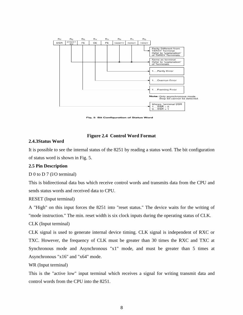
Figure 2.4 Control Word Format
2.4.3Status Word It is possible to see the internal status of the 8251 by reading a status word. The bit configuration
of status word is shown in Fig. 5. 2.5 Pin Description D 0 to D 7 (l/O terminal) This is bidirectional data bus which receive control words and transmits data from the CPU and
sends status words and received data to CPU. RESET (Input terminal) A "High" on this input forces the 8251 into "reset status." The device waits for the writing of
"mode instruction." The min. reset width is six clock inputs during the operating status of CLK. CLK (Input terminal) CLK signal is used to generate internal device timing. CLK signal is independent of RXC or
TXC. However, the frequency of CLK must be greater than 30 times the RXC and TXC at
Synchronous mode and Asynchronous "x1" mode, and must be greater than 5 times at
Asynchronous "x16" and "x64" mode. WR (Input terminal) This is the "active low" input terminal which receives a signal for writing transmit data and
control words from the CPU into the 8251.

9
RD (Input terminal)
This is the "active low" input terminal which receives a signal for reading receive data and status
words from the 8251. C/D (Input terminal) This is an input terminal which receives a signal for selecting data or command words and status
words when the 8251 is accessed by the CPU. If C/D = low, data will be accessed. If C/D = high,
command word or status word will be accessed. CS (Input terminal) This is the "active low" input terminal which selects the 8251 at low level when the CPU
accesses. Note: The device won’t be in "standby status"; only setting CS = High. TXD (output terminal) This is an output terminal for transmitting data from which serial-converted data is sent out. The
device is in "mark status" (high level) after resetting or during a status when transmit is disabled.
It is also possible to set the device in "break status" (low level) by a command. TXRDY (output terminal) This is an output terminal which indicates that the 8251is ready to accept a transmitted data
character. But the terminal is always at low level if CTS = high or the device was set in "TX
disable status" by a command. Note: TXRDY status word indicates that transmit data character is
receivable, regardless of CTS or command. If the CPU writes a data character, TXRDY will be
reset by the leading edge or WR signal. TXEMPTY (Output terminal) This is an output terminal which indicates that the 8251 has transmitted all the characters and had
no data character. In "synchronous mode," the terminal is at high level, if transmit data
characters are no longer remaining and sync characters are automatically transmitted. If the CPU
writes a data character, TXEMPTY will be reset by the leading edge of WR signal. Note : As the
transmitter is disabled by setting CTS "High" or command, data written before disable will be
sent out. Then TXD and TXEMPTY will be "High". Even if a data is written after disable, that
data is not sent out and TXE will be "High".After the transmitter is enabled, it sent out. (Refer to
Timing

10
Chart of Transmitter Control and Flag Timing)
TXC (Input terminal) This is a clock input signal which determines the transfer speed of transmitted data. In
"synchronous mode," the baud rate will be the same as the frequency of TXC. In "asynchronous
mode", it is possible to select the baud rate factor by mode instruction. It can be 1, 1/16 or 1/64
the TXC. The falling edge of TXC sifts the serial data out of the 8251. RXD (input terminal) This is a terminal which receives serial data. RXRDY (Output terminal) This is a terminal which indicates that the 8251 contains a character that is ready to READ. If the
CPU reads a data character, RXRDY will be reset by the leading edge of RD signal. Unless the CPU reads a data character before the next one is received completely, the preceding
data will be lost. In such a case, an overrun error flag status word will be set. RXC (Input terminal) This is a clock input signal which determines the transfer speed of received data. In
"synchronous mode," the baud rate is the same as the frequency of RXC. In "asynchronous
mode," it is possible to select the baud rate factor by mode instruction. It can be 1, 1/16, 1/64 the
RXC. SYNDET/BD (Input or output terminal) This is a terminal whose function changes according to mode. In "internal synchronous mode."
this terminal is at high level, if sync characters are received and synchronized. If a status word is
read, the terminal will be reset. In "external synchronous mode, "this is an input terminal. A
"High" on this input forces the 8251 to start receiving data characters. In "asynchronous mode," this is an output terminal which generates "high level"output upon the
detection of a "break" character if receiver data contains a "low-level" space between the stop
bits of two continuous characters. The terminal will be reset, if RXD is at high level. After Reset
is active, the terminal will be output at low level.

11
DSR (Input terminal) This is an input port for MODEM interface. The input status of the terminal can be recognized
by the CPU reading status words. DTR (Output terminal) This is an output port for MODEM interface. It is possible to set the status of DTR by a
command. CTS (Input terminal) This is an input terminal for MODEM interface which is used for controlling a transmit circuit.
The terminal controls data transmission if the device is set in "TX Enable" status by a command.
Data is transmitable if the terminal is at low level. RTS (Output terminal) This is an output port for MODEM interface. It is possible to set the status RTS by a command.
Fig 2.5 Pin Diagram of 8251

12
2.6 DMA Controller
• The DMA I/O technique provides direct access to the memory while the microprocessor
is temporarily disabled.
• This chapter also explains the operation of disk memory systems and video systems that
are often DMA-processed.
• Disk memory includes floppy, fixed, and optical disk storage. Video systems
include digital and analog monitors. 2.6.1 Pin Details of DMA( 8237) Figure 2.6Pin Diagarm of DMA
A DMA controller is a device, usually peripheral to a CPU that is programmed to perform a
sequence of data transfers on behalf of the CPU. A DMA controller can directly access memory
and is used to transfer data from one memory location to another, or from an I/O device to
memory and vice versa. A DMA controller manages several DMA channels, each of which can
be programmed to perform a sequence of these DMA transfers. Devices, usually I/O peripherals,
that acquire data that must be read (or devices that must output data and be written to) signal the
DMA controller to perform a DMA transfer by asserting a hardware DMA request (DRQ) signal.
A DMA request signal for each channel is routed to the DMA controller. This signal is
monitored and responded to in much the same way that a processor handles interrupts. When the

13
DMA controller sees a DMA request, it responds by performing one or many data transfers from
that I/O device into system memory or vice versa. Channels must be enabled by the processor for
the DMA controller to respond to DMA requests. The number of transfers performed, transfer
modes used, and memory locations accessed depends on how the DMA channel is programmed.
A DMA controller typically shares the system memory and I/O bus with the CPU and has both
bus master and slave capability. In bus master mode, the DMA controller acquires the system bus (address, data, and control
lines) from the CPU to perform the DMA transfers. Because the CPU releases the system bus for
the duration of the transfer, the process is sometimes referred to as cycle stealing. In bus slave mode, the DMA controller is accessed by the CPU, which programs the DMA
controller's internal registers to set up DMA transfers. The internal registers consist of source and
destination address registers and transfer count registers for each DMA channel, as well as
control and status registers for initiating, monitoring, and sustaining the operation of the DMA
controller.
Figure 2.7 Block Diagram

14
DMA Controller Operation Steps in a Typical DMA cycle Device wishing to perform DMA asserts the processors bus request signal.
1. Processor completes the current bus cycle and then asserts the bus grant signal
to the device. 2. The device then asserts the bus grant ack signal.
3. The processor senses in the change in the state of bus grant ack signal and starts
listening to the data and address bus for DMA activity. 4. The DMA device performs the transfer from the source to destination address.
5. During these transfers, the processor monitors the addresses on the bus and checks if
any location modified during DMA operations is cached in the processor. If the
processor detects a cached address on the bus, it can take one of the two actions:
Processor invalidates the internal cache entry for the address involved in DMA write
operation
Processor updates the internal cache when a DMA write is detected 6. Once the DMA operations have been completed, the device releases the bus by
asserting the bus release signal.
Reference Books:
1.Ramesh S Gaonkar, Microprocessor Architecture, Programming and application with 8085, 4»
Edition, Penram International Publishing, New Delhi, 2000
2. Kennith J. Ayala, 8051 Microcontroller, Thomson, 2005.
3. Dougles V. Hall, Microprocessor and Interfacing, Tata MC Graw Hill Publication, 2.‹Edition,
1992.
4. Charless M. Gilmore, “Microprocessor Principle and application, McGraw Hill publication,
1995.
5. A.NagoorKani, Microprocessor & Microcontroller, Tata Mc Graw Hill, 3«Edition, 2012
6. B. Ram, Fundamentals of Microprocessors and Microcomputers, Dhanpat Rai Publications,
2001.
1
SCHOOL OF BIO AND CHEMICAL ENGINEERING
DEPARTMENT OF BIOMEDICAL ENGINEERING
UNIT- IIII
INTRODUCTION TO 8086
Architecture of 8086 - Registers set of 8086 - Special function of general purpose register -
Addressing modes of 8086 - Instruction set - pin diagram of 8086 - Timing diagram- memory
read, memory write, l/O read and l/O write - Minimum and Maximum mode of operation
Interrupts of 8086.
Fundamentals of Microprocessor and Microcontroller – SEC1323

2
3.1 8086 Microprocessor Architecture
Intel 8086 was the first 16-bit microprocessor introduced by Intel in 1978. The 8086 architecture supports
• 16-bit ALU.
• a set of 16 bit registers
• provides segmented memory addressing scheme
• a rich instruction set.
• Powerful interrupt structure
• Fetched instruction queue for overlapped fetching and execution step. The internal block diagram units inside the 8086 microprocessor is shown in the figure.
Figure 3.1 Architecture of 8086 Microprocessor
The architecture of 8086 can be divided into two parts
• Bus Interface unit (BIU)
• Execution unit (EU)
The bus interface unit is responsible for physical address calculations and a predecoding
3
instruction byte queue ( 6 bytes long).The bus interface unit makes the system bus signal
available for external devices.The 8086 addresses a segmented memory. The complete physical
address which is 20-bits long is generated using segment and offset registers, each 16-bits long. 1.1 Generation a Physical Address:
• The content of segment register (segment address) is shifted left bit-wise four times.
• The content of an offset register (offset address) is added to the result of the previous
shift operation. The segment register indicates the base address of a particular segment and CS, DS, SS and ES
are used to keep the segment address. The offset indicates the distance of the required memory
location in the segment from the base address, and the offset may be the content of register IP,
BP, SI, DI and SP. Once the opcode is fetched and decoded, the external bus becomes free while
the Execution Unit is executing the instruction. While the fetched instruction is executed
internally, the external bus is used to fetch the machine code of the next instruction and arrange it
in a queue called as predecoded instruction byte queue.This is a 6 byte long queue, works in
first-in first-out policy.While the opcode is fetched by the bus interface unit (BIU), the execution
unit (EU) executes the previously decoded instruction concurrently. The execution unit contains.
b) the register set of 8086 except segment registers and IF.
c) a 16-bit ALU to perform arithmetic & logic operation
d) 16-bit flag register reflects the results of execution by the ALU.
e) the decoding units decodes the op-code bytes issued from the instruction byte queue.
f) the timing and control unit generates the necessary control signals to execute the
instruction op-code received from the queue. The execution unit may pass the results to the bus interface unit for storing them in memory. 3.2Memory Segmentation: The size of address bus of 8086 is 20 and is able to address 1 Mbytes ( 220 ) of physical
memory.The compete 1 Mbytes memory can be divided into 16 segments, each of 16 Kbytes
size.The addresses of the segment may be assigned as 0000H to F000H respectively.The offset
values are from 0000H to FFFFFH.If the segmentation is done as per above mentioned way, the
segments are called non-overlapping segments.

4
In some cases segment may overlap also. Suppose a segment starts at a particular address and its
maximum size can go up to 64 Kbytes. But if another segment starts before this 64 Kbytes
location of the first segment, the two segments are said to be overlapping segment.
The main advantages of the segmented memory scheme are as follows:
a Allows the memory capacity to be 1 Mbyte although the actual addresses to be handled
are of 16-bit size
b Allows the placing of code data and stack portions of the same program in different parts
(segments) of memory, for data and code protection.
c Permits a program and/ or its data to be put into different areas of memory each time
program is executed, ie, provision for relocation may be done. 3.3 Flag Register A 16 flag register is used in 8086. It is divided into two parts .
• Condition code or status flags
• Machine control flags The condition code flag register is the lower byte of the 16-bit flag register. The condition code
flag register is identical to 8085 flag register, with an additional overflow flag.The control flag
register is the higher byte of the flag register. It contains three flags namely direction flag(D),
interrupt flag (I) and trap flag (T).The complete bit configuration of 8086 is shown in the figure 2
Fig 3.2 Flags Format

5
S- Sign Flag : This flag is set, when the result of any computation is negative. Z- Zero Flag: This flag is set, if the result of the computation or comparison performed by the
previous instruction is zero. P- Parity Flag: This flag is set to 1, if the lower byte of the result contains even number of 1‘s. C- Carry Flag: This flag is set, when there is a carry out of MSB in case of addition or a borrow
in case of subtraction. T- Tarp Flag: If this flag is set, the processor enters the single step execution mode. I- Interrupt Flag: If this flag is set, the maskable interrupt are recognized by the CPU, otherwise
they are ignored. D- Direction Flag: This is used by string manipulation instructions. If this flag bit is ‗0‘, the
string is processed beginning from the lowest address to the highest address, i.e., auto
incrementing mode. Otherwise, the string is processed from the highest address towards the
lowest address, i.e., auto incrementing mode. AC-Auxilary Carry Flag: This is set, if there is a carry from the lowest nibble, i.e, bit three during
addition, or borrow for the lowest nibble, i.e, bit three, during subtraction. O- Over flow Flag: This flag is set, if an overflow occurs, i.e, if the result of a signed operation is
large enough to accommodate in a destination register. The result is of more than 7-bits in
size in case of 8-bit signed operation and more than 15-bits in size in case of 16-bit sign
operations, then the overflow will be set.
3.4 Pin Details of 8086
The 8086 is a 16-bit microprocessor. These microprocessors operate in single processor or
multiprocessor configurations to achieve high performance. The pin configuration of 8086 is
shown in the figure. Some of the pins serve a particular function in minimum mode (single
processor mode) and others function in maximum mode (multiprocessor mode).

6
Figure 3.3 Pin Configuration 3.5 Description of signals of 8086
AD7 AD0 The address/ data bus lines are the multiplexed address data bus and contain the
right most eight bit of memory address or data. The address and data bits are
separated by using ALE signal. AD15 AD8 The address/data bus lines compose the upper multiplexed address/data bus. This
lines contain address bit A15 A8 or data bus D15 D8 . The address and data bits are
separated by using ALE signal.
A19 / S 6 A18 / S3 The address/status bus bits are multiplexed to provide address signals A19 A16
and also status bits S 6 S3 . The address bits are separated from the status bits using
the ALE signals. The status bit S6 is always a logic 0, bit S5 indicates the condition of
the interrupt flag bit. The S4 and S3 combinedly indicate which segment register is
presently being used for memory access.
S4 S3 Funtion
0 0 Extra segment

7
0 1 Stack segment
1 0 Code or no segment
1 1 Data Segment
BHE / S7 The bus high enable (BHE) signal is used to indicate the transfer of data over the higher
order D15 D8 data bus. It goes low for the data transfer over D15 D8 and is used to derive
chip select of odd address memory bank or peripherals.
A0 Indication
BH
E
0 0 Whole word
0 1 Upper byte from or to odd address
1 0 Lower byte from or to even address
1 1 None
RD : Read : whenever the read signal is at logic 0, the data bus receives the data from the
memory or 0 devices connected to the system
READY :This is the acknowledgement from the slow devices or memory that they have
completed the data transfer operation. This signal is active high.
INTR: Interrupt Request: Interrupt request is used to request a hardware interrupt of INTR is held
high when interrupt enable flag is set, the 8086 enters an interrupt acknowledgement cycle after
the current instruction has completed its execution. TEST : This input is tested by ―WAIT‖ instruction. If the TEST input goes low; execution will
continue. Else the processor remains in an idle state.
NMI- Non-maskable Interrupt: The non-maskable interrupt input is similar to INTR except that
the NMI interrupt does not check for interrupt enable flag is at logic 1, i.e, NMI is not maskable
internally by software. If NMI is activated, the interrupt input uses interrupt vector 2.
8
RESET: The reset input causes the microprocessor to reset itself. When 8086 reset, it restarts the
execution from memory location FFFF0H. The reset signal is active high and must be
active for at least four clock cycles. CLK : Clock input: The clock input signal provides the basic timing input signal for processor
and bus control operation. It is asymmetric square wave with 33% duty cycle.
Vcc 5V power supply for the operation of the internal circuit MN / MX : The minimum/maximum mode signal to select the mode of operation either in
minimum or maximum mode configuration. Logic 1 indicates minimum mode.
3.6 Minimum Mode of 8086 :
M / IO -Memory/IO M / IO signal selects either memory operation or o operation. This line
indicates that the microprocessor address bus contains either a memory address or an o
port address. Signal high at this pin indicates a memory operation. This line is logically
equivalent to S2 in maximum mode. INTA - Interrupt acknowledge: The interrupt acknowledge signal is a response to the INTR input
signal. The INTA signal is normally used to gate the interrupt vector number onto the data
bus in response to an interrupt request.
ALE- Address Latch Enable: This output signal indicates the availability of valid address on the
address/data bus, and is connected to latch enable input of latches. DT / R : Data transmit/Receive: This output signal is used to decide the direction of date flow
through the bi-directional buffer. DT / R 1 indicates transmitting and DT / R 0 indicates
receiving the data. DEN Data Enable: Data bus enable signal indicates the availability of valid data over the
address/data lines. HOLD: The hold input request a direct memory access(DMA). If the hold signal is at logic 1, the
micro process stops its normal execution and places its address, data and control bus at
the high impedance state.
9
HLDA: Hold acknowledgement indicates that 8086 has entered into the hold state.
3.7 Maximum Mode of 8086:
S 2 , S1 , S0 - Status lines: These are the status lines that reflect the type of operation being carried
out by the processor. These status lines are encoded as follows
Function
S2 S1 S0
0 0 0 Interrupt Acknowledge
0 0 1 Read o port
0 1 0 Write o port
0 1 1 Halt
1 0 0 Code Access
1 0 1 Read memory
1 1 0 Write memory
1 1 1 passive
LOCK : The lock output is used to lock peripherals off the system, ie, the other system bus
masters will be prevented from gaining the system bus.
QS1 and QS0 - Queue status: The queue status bits shows the status of the internal instruction
queue. The encoding of these signals is as follows
QS1 QS0 Function
0 0 No operation, queue is idle
0 1 First byte of opcode

10
1 0 Queue is empty
1 1 Subsequent byte of opcode
RQ / GT1 and RQ / GT 0 - request/Grant: The request/grant pins are used by other local bus
masters to force the processor to release the local bus at the end of the processors
current bus cycle. These lines are bi-directional and are used to both request and grant
a DMA operation. RQ / GT 0 is having higher priority than RQ / GT1
Physical Memory Organization In an 8086 based system, the 1Mbyte memory is physically organized as odd bank and even
bank, each of 512kbytes, addressed in parallel by the processor. Byte data with even address is transferred on D7 D0 and byte data with odd address is
transferred on D15 D8 .The processor provides two enable signals, BHE and A0 for selecting of
either even or odd or both the banks.
A0 Indication
BH
E
0 0 Whole word
0 1 Upper byte from or to odd address
1 0
Lower byte from or to even address
1 1 None
Register Set of 8086 General Data Registers:
The registers AX, BX,CX and DX are the general purpose 16-bit registers.
AX is used as 16-bit accumulator. The lower 8-bit is designated as AL and higher 8-bit is
designated as AH. AL can be used as an 8-bit accumulator for 8-bit operation. All data register can be used as either 16 bit or 8 bit. BX is a 16 bit register, but BL indicates the
lower 8-bit of BX and BH indicates the higher 8-bit of BX.

11
The register CX is used default counter in case of string and loop instructions. The register BX is used as offset storage for forming physical address in case of certain
addressing modes. DX register is a general purpose register which may be used as an implicit operand or
destination in case of a few instructions. Segment Registers:
The 8086 architecture uses the concept of segmented memory. 8086 able to address to address a
memory capacity of 1 megabyte and it is byte organized. This 1 megabyte memory is divided
into 16 logical segments. Each segment contains 64 kbytes of memory. There are four segment
register in 8086
Code segment register (CS)
Data segment register (DS)
Extra segment register (ES)
Stack segment register (SS) Code segment register (CS): is used fro addressing memory location in the code segment of the
memory, where the executable program is stored. Data segment register (DS): points to the data segment of the memory where the data is stored.
Extra Segment Register (ES) : also refers to a segment in the memory which is another data
segment in the memory. Stack Segment Register (SS): is used fro addressing stack segment of the memory. The stack
segment is that segment of memory which is used to store stack data. While addressing any location in the memory bank, the physical address is calculated from two
parts:
• The first is segment address, the segment registers contain 16-bit segment base addresses,
related to different segment.
• The second part is the offset value in that segment. The advantage of this scheme is that in place of maintaining a 20-bit register for a physical
address, the processor just maintains two 16-bit registers which is within the memory capacity of
the machine.

12
Pointers and Index Registers. The pointers contain offset within the particular segments.
• The pointer register IP contains offset within the code segment.
• The pointer register BP contains offset within the data segment.
• He pointer register SP contains offset within the stack segment. The index registers are used as general purpose registers as well as for offset storage in case of
indexed, base indexed and relative base indexed addressing modes. The register SI is used to
store the offset of source data in data segment. The register DI is used to store the offset of destination in data or extra segment. The index registers are particularly useful for string manipulation. 3.8 Various addressing modes of 8086 Various addressing modes of 8086/8088 • Register Addressing mode • Immediate Addressing mode • Register Indirect Addressing mode • Direct Addressing mode • Indexed Addressing mode • Base Relative Addressing mode • Base Indexed Addressing mode Register Addressing Mode Data transfer using registers is called register addressing mode. Here operand value is present in register. For example MOV AL,BL; MOV AX,BX;
immediate Addressing mode When data is stored in code segment instead of data segment immediate addressing mode is
used. Here operand value is present in the instruction. For example MOV AX, 12345;
Direct Addressing mode

13
When direct memory address is supplied as part of the instruction is called direct addressing
mode. MOV AX, [1234]; ADD AX, [1234]; Register Indirect Addressing mode Here operand offset is given in a cpu register. Register used are BX, SI(source index), DI(destination index), or BP(base pointer). BP holds offset w.r.t Stack segment, but SI,DI and BX refer to data segment. For example MOV [BX],AX; ADD AX, [SI]; Indexed Addressing mode Here operand offset is given by a sum of a value held in either SI, or DI register and a constant
displacement specified as an operand. For example Lets take arrays as an example. This is very efficient way of accessing arrays. My_array DB ‘1’, ‘2’, ‘3’,’4,’5’; MOV SI, 3; MOV AL, My_array[3]; So AL holds value 4. Base Relative Addressing mode Operand offset given by a sum of a value held either in BP, or BX and a constant offset sepecified as an operand. For example MOV AX,[BP+1]; JMP [BX+1]; Base Indexed Here operand offset is given by sum of either BX or BP with either SI or DI. For example
MOV AX, [BX+SI]
JMP [BP+DI]

14
3.9 Maximum Mode and Minimum Mode
In the maximum mode, the 8086 is operated by strapping the MN/MX* pin to ground. In this
mode, the processor derives the status signals S2*, S1* and S0*. Another chip called bus
controller derives the control signals using this status information. In the maximum mode, there
may be more than one microprocessor in the system configuration. The other components in the
system are the same as in the minimum mode system. The general system organization is as
shown in the figure 4.
The basic functions of the bus controller chip IC8288, is to derive control signals like RD* and
WR* (for memory and I/O devices), DEN*, DT/R*, ALE, etc. using the information made
available by the processor on the status lines. The bus controller chip has input lines S2*, S1*
and S0* and CLK. These inputs to 8288 are driven by the CPU. It derives the outputs ALE,
DEN*, DT/R*, MWTC*, AMWC*, IORC*, IOWC* and AIOWC*. The AEN*, IOB and CEN
pins are specially useful for multiprocessor systems. AEN* and IOB are generally grounded.
CEN pin is usually tied to +5V.

15
Fig 3.4 Maximum Mode 8086 System The significance of the MCE/PDEN* output depends upon the status of the IOB pin. If IOB is
grounded, it acts as master cascade enable to control cascaded 8259A; else it acts as peripheral
data enable used in the multiple bus configurations. INTA* pin is used to issue two interrupt

16
IORC*, IOWC* are I/O read command and I/O write command signals respectively. These
signals enable an IO interface to read or write the data from or to the addressed port. The
MRDC*, MWTC* are memory read command and memory write command signals respectively and may be used as memory read and write signals. All these command signals instruct the
memory to accept or send data from or to the bus. For both of these write command signals, the
advanced signals namely AIOWC* and AMWTC* are available. They also serve the same
purpose, but are activated one clock cycle earlier than the IOWC* and MWTC* signals,
respectively. The maximum mode system is shown in fig. 4.
The maximum mode system timing diagrams are also divided in two portions as read (input) and
write (output) timing diagrams. The address/data and address/status timings are similar to the
minimum mode. ALE is asserted in T1, just like minimum mode. The only difference lies in the
status signals used and the available control and advanced command signals. The fig. 5 shows
the maximum mode timings for the read operation while the fig. 6 shows the same for the write
operation.
The read cycle begins in T1 with the assertion of ALE (Address latch enable ) and M/IO signal
for memory or input-output process. During the negative going edge of the signal ,the valid
address is latched on the local bus. The BHE or bus high enable and Ao signal addresses low ,
high or both bytes. 3.10 Timing Diagram of 8086 Microprocessor :

17
3.10.1. Memory Read Timing Diagram
Fig 3.5 Timing Diagram

18
3.10.2Memory Write Timing Diagram : Fig 3.6 Timing Diagram

19
3.10.3 IO Read Timing Diagram
Fig. 3.7 Memory Read Timing for IO Read

20
3.10.4 IO Write Timing Diagram
Fig. 3.8 Timing Diagram for IO Write

21
Reference Books :
1.Ramesh S Gaonkar, Microprocessor Architecture, Programming and application with 8085, 4»
Edition, Penram International Publishing, New Delhi, 2000
2. Kennith J. Ayala, 8051 Microcontroller, Thomson, 2005.
3. Dougles V. Hall, Microprocessor and Interfacing, Tata MC Graw Hill Publication, 2.‹Edition,
1992.
4. Charless M. Gilmore, “Microprocessor Principle and application, McGraw Hill publication,
1995.
5. A.NagoorKani, Microprocessor & Microcontroller, Tata Mc Graw Hill, 3«Edition, 2012
6. B. Ram, Fundamentals of Microprocessors and Microcomputers, Dhanpat Rai Publications,
2001.

1
SCHOOL OF BIO AND CHEMICAL ENGINEERING
DEPARTMENT OF BIOMEDICAL ENGINEERING
UNIT -IV
Introduction to 8 - bit Microcontrollers - 8051 MicrocArchitecture - Registers set of 8051 -
modes of Timer operation - Serial Port operation - Interrupt Structure of 8051 - Memory and
Input / Output Interfacing of 8051.
Fundamentals of Microprocessor and Microcontroller – SEC1323

2
4.1 8051 Microcontroller Architecture
An 8051 microcontroller has the following 12 major components:
• ALU (Arithmetic and Logic Unit)
• PC (Program Counter)
• Registers
• Timers and counters
• Internal RAM and ROM
• Four general purpose parallel input/output ports
• Interrupt control logic with five sources of interrupt
• Serial date communication
• PSW (Program Status Word)
• Data Pointer (DPTR)
• Stack Pointer (SP)

3
Fig 4.1: 8051 Microcontroller Diagram
Figure 4.1 Architecture Diagram
All arithmetic and logical functions are carried out by the ALU. Addition, subtraction with carry,
and multiplication come under arithmetic operations.Logical AND, OR and exclusive OR (XOR)
come under logical operations. 4.1.1.Program Counter (PC)
A program counter is a 16-bit register and it has no internal address. The basic function of
program counter is to fetch from memory the address of the next instruction to be executed. The
PC holds the address of the next instruction residing in memory and when a command is
encountered, it produces that instruction. This way the PC increments automatically, holding the
address of the next instruction.

4
4.1.2 . Registers
Registers are usually known as data storage devices. 8051 microcontroller has 2 registers,
namely Register A and Register B. Register A serves as an accumulator while Register B
functions as a general purpose register. These registers are used to store the output of
mathematical and logical instructions. The operations of addition, subtraction, multiplication and
division are carried out by Register A. Register B is usually unused and comes into picture only
when multiplication and division functions are carried out by Register A. Register A also
involved in data transfers between the microcontroller and external memory. 8051 microcontroller also has 7 Special Function Registers (SFRs). They are:
• Serial Port Data Buffer (SBUF)
• Timer/Counter Control (TCON)
• Timer/Counter Mode Control (TMOD)
• Serial Port Control (SCON)
• Power Control (PCON)
• Interrupt Priority (IP)
• Interrupt Enable Control (IE) 4.1.3 . Timers and Counters
Synchronization among internal operations can be achieved with the help of clock circuits which
are responsible for generating clock pulses. During each clock pulse a particular operation will
be carried out, thereby, assuring synchronization among operations. For the formation of an
oscillator, we are provided with two pins XTAL1 and XTAL2 which are used for connecting a
resonant network in 8051 microcontroller device. In addition to this, circuit also consists of four
more pins. Internal operations can be synchronized using clock circuits which produce clock pulses. With
each clock pulse, a particular function will be accomplished and hence synchronization is
achieved. There are two pins XTAL1 and XTAL2 which form an oscillator circuit which connect
to a resonant network in the microcontroller. The circuit also has 4 additional pins -
• EA: External enable
• ALE: Address latch enable

5
b) PSEN: Program store enable and c) RST: Reset Quartz crystal is used to generate periodic clock pulses.
5. Internal RAM and ROM 4.1.4 ROM
A code of 4K memory is incorporated as on-chip ROM in 8051. The 8051 ROM is a non-
volatile memory meaning that its contents cannot be altered and hence has a similar range of
data and program memory, i.e, they can address program memory as well as a 64K separate
block of data memory. 4.1.5 RAM
The 8051 microcontroller is composed of 128 bytes of internal RAM. This is a volatile memory
since its contents will be lost if power is switched off. These 128 bytes of internal RAM are
divided into 32 working registers which in turn constitute 4 register banks (Bank 0-Bank 3) with
each bank consisting of 8 registers (R0 - R7). There are 128 addressable bits in the internal
RAM. 4.1.6 I/O Ports The 8051 microcontroller has four 8-bit input/output ports.
PORT P0: When there is no external memory present, this port acts as a general purpose
input/output port. In the presence of external memory, it functions as a multiplexed address and
data bus. It performs a dual role.
PORT P1: This port is used for various interfacing activities. This 8-bit port is a normal I/O port
i.e. it does not perform dual functions. PORT P2: Similar to PORT P0, this port can be used as a general purpose port when there is no
external memory but when external memory is present it works in conjunction with PORT PO as
an address bus. This is an 8-bit port and performs dual functions. PORT P3: PORT P3 behaves as a dedicated I/O port
6
4.2.Instruction set of 8051 4.2.1 Data Transfer Instructions: MOV A,Rn Move register to accumulator 1
MOV A,dirct Move direct byte to accumulator
MOV A,@RiMove indirect RAM to accumulator
MOV A,#daa Move immediate data to accumulator
MOV Rn,A Move accumulator to register 1
MOV Rn,direct Move direct byte to register
MOV Rn,#data Move immediate data to register
MOV direct,A Move accumulator to direct byte
MOV direct,Rn Move register to direct byte 2
MOV direct,direct Move direct byte to direct byte
MOV direct,@Ri Move indirect RAM to direct byte
MOV direct,#data Move immediate data to direct byte
MOV @Ri,AMove accumulator to indirect RAM 1
MOV @Ri,direct Move direct byte to indirect RAM
MOV @Ri, #data Move immediate data to indirect RAM
MOV DPTR, #data16
Load data pointer with a 16-bit
constant
MOVC A,@A DPTR
Move code byte relative to DPTR to
accumulator
MOVC A,@A + PC Move code byte relative to PC to accumulator
MOVX A,@RiMove external RAM (8-bit addr.) to A
MOVX A,@DPTR Move external RAM (16-bit addr.) to A
MOVX @Ri,AMove A to external RAM (8-bit addr.)

7
MOV
X
@DPTR,A Move A to external RAM (16-bit
addr.)
PUSH direct Push direct byte onto stack
POP direct Pop direct byte from stack
XCH A,Rn Exchange register with accumulator
XCH
A,dire
ct Exchange direct byte with accumulator
XCH A,@RiExchange indirect RAM with accumulator
XCHDA,@RiExchange low-order nibble indir. RAM with A 4.2.2 Arithmetic Instructions: ADD A,Rn
ADD
A,direct ADD A,@Ri ADD
A,#data ADDC A,Rn
ADDC A,direct ADDC A,@Ri ADDC A,#data
SUBB A,Rn
SUBB
A,direct
SUBB
A,@Ri
Adds the register to the accumulator Adds the direct byte to the accumulator Adds the indirect RAM to the accumulator Adds the immediate data to the accumulator
Adds the register to the accumulator with a carry flag Adds the direct byte to the accumulator with a carry flag Adds the indirect RAM to the accumulator with a carry flag Adds the immediate data to the accumulator with a carry flag Subtracts the register from the accumulator with a borrow Subtracts the direct byte from the accumulator with a borrow Subtracts the indirect RAM from the
accumulator with a borrow

8
SUBB Subtracts the immediate data from the
A,#dat
a accumulator with a borrow
INC A Increments the accumulator by 1
INC
Rn Increments the register by 1
INC
Rx Increments the direct byte by 1
INC @Ri Increments the indirect RAM by 1
DEC A Decrements the accumulator by 1
DEC
Rn Decrements the register by 1
DEC
Rx Decrements the direct byte by 1
DEC @Ri Decrements the indirect RAM by 1
INC DPTR Increments the Data Pointer by 1
MUL AB Multiplies A and B
DIV
AB Divides A by B
DA A Decimal adjustment of the accumulator
4.2.3 Logical
Instructions:
ANL A,Rn AND register to accumulator
ANL A,direct AND direct byte to accumulator
ANL A,@RiAND indirect RAM to accumulator
ANL A,#data AND immediate data to accumulator

9
4.2.4 Boolean Variable Manipulation
ANL direct,#data AND immediate data to direct byte
ORL A,Rn OR register to accumulator
ORL
A,dire
ct OR direct byte to accumulator
ORL A,@RiOR indirect RAM to accumulator
ORL
A,#dat
a OR immediate data to accumulator
ORL
direct,
A OR accumulator to direct byte
ORL direct,#data OR immediate data to direct byte
XRL A,Rn Exclusive OR register to accumulator
XRL
A
direct
Exclusive OR direct byte to
accumulator
XRL A,@RiExclusive OR indirect RAM to accumulator
XRL
A,#dat
a
Exclusive OR immediate data to
accumulator
XRL
direct,
A
Exclusive OR accumulator to direct
byte
XRL direct,#data
Exclusive OR immediate data to direct
byte
CLR A Clear accumulator
CPL A Complement accumulator
RL A Rotate accumulator left
RLC A Rotate accumulator left through carry
SETB C Set carry flag
SETB bit Set direct bit
CPL C Complement carry flag
CPL bit Complement direct bit2
ANL C,bit AND direct bit to carry flag
ANL
C,/bi
t
AND complement of direct bit to
carry
ORL C,bit OR direct bit to carry flag
ORL
C,/bi
t OR complement of direct bit to carry
MOV C,bit Move direct bit to carry flag

10
LCAL addr11 Absolute subroutine call
LCAL addr16 Long subroutine call
RET Return from subroutine
RETI Return from interrupt
AJMP addr11 Absolute jump2
LJMP addr16 Long iump
SJMP rel Short jump (relative addr.)
JMP
@A + DPTR Jump indirect relative to the
DPTR
JZ rel Jump if accumulator is zero
JNZ rel Jump if accumulator is not zero
JC rel Jump if carry flag is set
JNC rel Jump if carry flag is not set

11
JNB bit,rel Jump if direct bit is not set
JBC bit,rel Jump if direct bit is set and clear bit
CJNE A,direct,rel
Compare direct byte to A and jump if not
equal
4.2.5 Machine
Control
CJNE A,#data,rel
Compare immediate to A and jump if not
equal
CJNE Rn,#data rel Compare immed. to reg. and jump if not equal
CJNE
@Ri,#data,rel Compare immed. to ind. and jump if not
equal
DJNZ Rn,rel Decrement register and jump if not zero
DJNZ direct,rel Decrement direct byte and jump if not zero
NOP No operation

12
4.3.Register Set 8051
4.3.1 Register A/Accumulator The most important of all special function registers, that’s the first comment about
Accumulatorwhich is also known as ACC or A. The Accumulator (sometimes referred to as
Register A also) holds the result of most of arithmetic and logic operations. ACC is usually
accessed by direct addressing and its physical address is E0H. Accumulator is both byte and bit
addressable. You can understand this from the figure shown below. To access the first bit (i.e
bit 0) or to access accumulator as a single byte (all 8 bits at once), you may use the same
physical address E0H. Now if you want to access the second bit (i.e bit 1), you may use E1H
and for third bit E2H and so on.
Figure 4.2 Register Format
4.3.2 Register B The major purpose of this register is in executing multiplication and division. The 8051 micro
controller has a single instruction for multiplication (MUL) and division (DIV). If you are
familiar with 8085, you may now know that multiplication is repeated addition, where as
division is repeated subtraction. While programming 8085, you may have written a loop to
execute repeated addition/subtraction to perform multiplication and division. Now here in 8051
you can do this with a single instruction.

13
Ex: MUL A,B – When this instruction is executed, data inside A and data inside B is multiplied
and answer is stored in A. Note: For MUL and DIV instructions, it is necessary that the two operands must be in A and B. Note: Follow this link if you are interested in knowing about differences between a
microprocessor and microcontroller. Register B is also byte addressable and bit addressable. To access bit o or to access all 8 bits (as
a single byte), physical address F0 is used. To access bit 1 you may use F1 and so on. Please
take a look at the picture below. Figure 4.3 Register B format
Note: Register B can also be used for other general purpose operations. Port Registers
As you may already know, there are 4 ports for 8051. If you are unfamiliar of the architecture of
8051 please read the following article:- The architecture of 8051 So 4 Input/Output ports named P0, P1, P2 and P3 has got four corresponding port registers with
same name P0, P1, P2 and P3. Data must be written into port registers first to send it out to any
other external device through ports. Similarly any data received through ports must be read from
port registers for performing any operation. All 4 port registers are bit as well as byte
addressable. Take a look at the figure below for a better understanding of port registers.

14
Figure 4.4 Port Register Format • The physical address of port 0 is 80 • The physical address of port 1 is 90 • And that of port 2 is A0 • And that of port 3 is B0
4.3.3 Stack Pointer Known popularly with an acronym SP, stack pointer represents a pointer to the the system stack.
Stack pointer is an 8 bit register, the direct address of SP is 81H and it is only byte addressable,
which means you cant access individual bits of stack pointer. The content of the stack pointer
points to the last stored location of system stack. To store something new in system stack, the SP
must be incremented by 1 first and then execute the “store” command. Usually after a system
reset SP is initialized as 07H and data can be stored to stack from 08H onwards. This is usually
a default case and programmer can alter values of SP to suit his needs.

15
4.3.4 Power Management Register (PCON) Power management using a microcontroller is something you see every day in mobile phones.
Haven’t you noticed and got wondered by a mobile phone automatically going into stand by
mode when not used for a couple of seconds or minutes ? This is achieved by power
management feature of the controller used inside that phone.
As the name indicates, this register is used for efficient power management of 8051 micro
controller. Commonly referred to as PCON register, this is a dedicated SFR for power
management alone. From the figure below you can observe that there are 2 modes for this
register :- Idle mode and Power down mode.
Figure 4.5 PCon Register format
Setting bit 0 will move the micro controller to Idle mode and Setting bit 1 will move the micro
controller to Power down mode.
4.3.5 Processor Status Word (PSW) Commonly known as the PSW register, this is a vital SFR in the functioning of micro controller.
This register reflects the status of the operation that is being carried out in the processor. The
picture below shows PSW register and the way register banks are selected using PSW register
bits – RS1 and RS0. PSW register is both bit and byte addressable. The physical address of PSW
starts from D0H. The individual bits are then accessed using D1, D2 … D7. The various
individual bits are explained below.
Figure 4.6 PSW Format
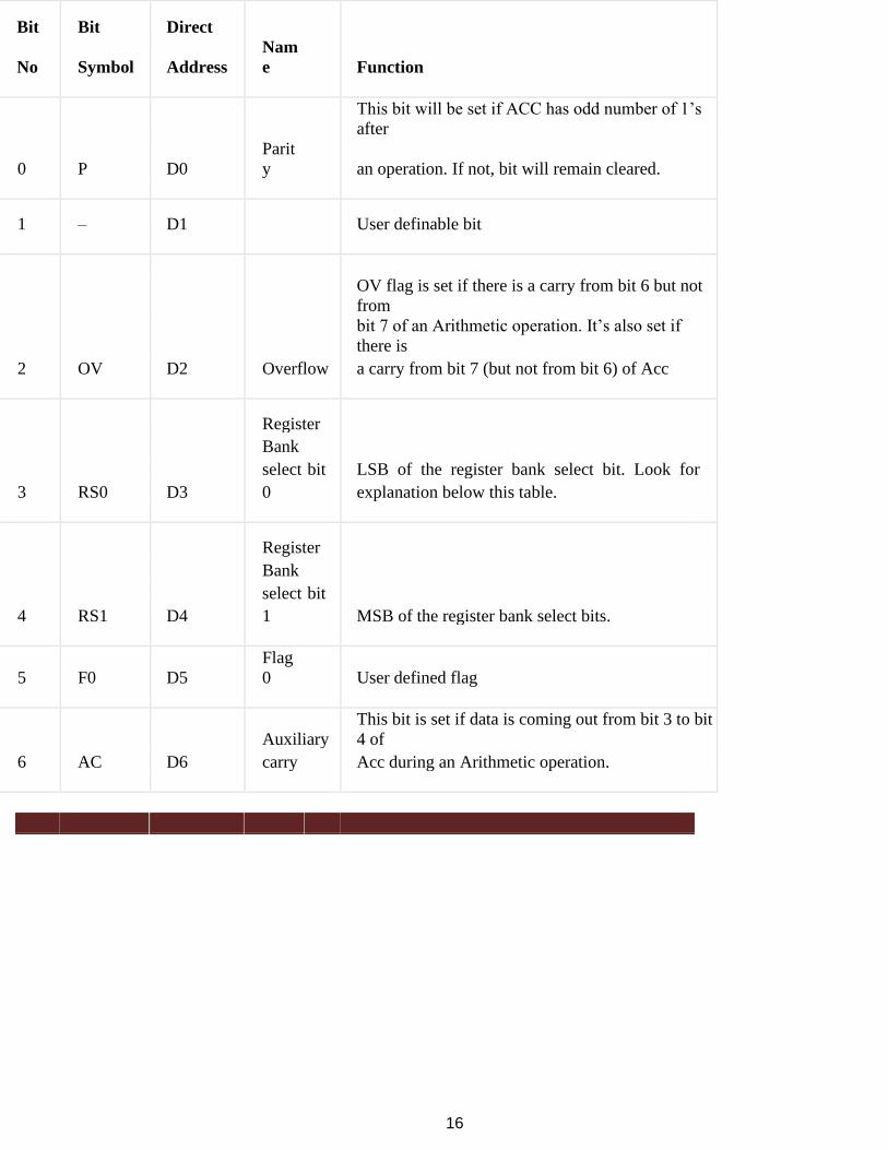
16
Bit Bit Direct
No Symbol Address
Nam
e Function
This bit will be set if ACC has odd number of 1’s
after
0 P D0
Parit
y an operation. If not, bit will remain cleared.
1 – D1 User definable bit
OV flag is set if there is a carry from bit 6 but not
from
bit 7 of an Arithmetic operation. It’s also set if
there is
2 OV D2 Overflow a carry from bit 7 (but not from bit 6) of Acc
Register
Bank
select bit LSB of the register bank select bit. Look for
3 RS0 D3 0 explanation below this table.
Register
Bank
select bit
4 RS1 D4 1 MSB of the register bank select bits.
5 F0 D5
Flag
0 User defined flag
Auxiliary
This bit is set if data is coming out from bit 3 to bit
4 of
6 AC D6 carry Acc during an Arithmetic operation.

17
Is set if data is coming out of bit 7 of Acc during
an
7
C
Y D7 Carry
Arithmetic
operation.
At a time registers can take value from R0,R1…to R7. You may already know there are 32 such
registers. So how you access 32 registers with just 8 variables to address registers? Here comes
the use of register banks. There are 4 register banks named 0,1,2 and 3. Each bank has 8
registers named from R0 to R7. At a time only one register bank can be selected. Selection of
register bank is made possible through PSW register bits PSW.3 and PSW.4, named as RS0 and
RS1.These two bits are known as register bank select bits as they are used to select register
banks. The picture will talk more about selecting register banks.So far we have discussed about
all major SFR’s in 8051. There many other still waiting! Please remember there are 21 SFR’s
and we have discussed only 9 specifically. The table below lists all other 12 SFR’s.

18
IP B8 Interrupt priority. Both bit addressing and byte addressing possible.
IE A8 Interrupt enable. Both bit addressing and byte addressing possible.
SBUF 99 Serial Input/Output buffer. Only byte addressing is possible.
Serial communication control. Both bit addressing and byte
addressing
SCON 98 possible.
TCON 88 Timer control. Both bit addressing and byte addressing possible.
TH0 8C Timer 0 counter (High). Only byte addressing is possible.
TL0 8A Timer 0 counter (Low). Only byte addressing is possible.
TH1 8D Timer 1 counter (High). Only byte addressing is possible.
TL1 8B Timer 1 counter (Low). Only byte addressing is possible.
TMOD 89 Timer mode select. Only byte addressing is possible.
4.4.8051 Modes of Timer operation
The 8051 has two timers: timer0 and timer1. They can be used either as timers or as counters.
Both timers are 16 bits wide. Since the 8051 has an 8-bit architecture, each 16-bit is accessed as
two separate registers of low byte and high byte. First we shall discuss about Timer0 registers.
Timer0 registers is a 16 bits register and accessed as low byte and high byte. The low byte is
referred as a TL0 and the high byte is referred as TH0. These registers can be accessed like any
other registers.

19
Figure 4.7 Timer 0
Timer1 registers is also a 16 bits register and is split into two bytes, referred to as TL1 and TH1. Figure 4.8 Timer 2
TMOD (timer mode) Register: This is an 8-bit register which is used by both timers 0 and 1 to
set the various timer modes. In this TMOD register, lower 4 bits are set aside for timer0 and the
upper 4 bits are set aside for timer1. In each case, the lower 2 bits are used to set the timer mode
and upper 2 bits to specify the operation.
Figure 4.9 TMOD Register
TMOD In upper or lower 4 bits, first bit is a GATE bit. Every timer has a means of starting and
stopping. Some timers do this by software, some by hardware, and some have both software and
hardware

20
controls. The hardware way of starting and stopping the timer by an external source is achieved
by making GATE=1 in the TMOD register. And if we change to GATE=0 then we do no need
external hardware to start and stop the timers.
The second bit is C/T bit and is used to decide whether a timer is used as a time delay
generator or an event counter. If this bit is 0 then it is used as a timer and if it is 1 then it is used
as a counter.
In upper or lower 4 bits, the last bits third and fourth are known as M1 and M0 respectively.
These are used to select the timer mode.
M0 M1 Mode Operating Mode
0 0 0
13-bit timer mode, 8-bit timer/counter THx and TLx as 5-bit
prescalar.
0 1 1
16-bit timer mode, 16-bit timer/counters THx and TLx are
cascaded;
There are no prescalar.
1 0 2
8-bit auto reload mode, 8-bit auto reload timer/counter; THx holds
a
value which is to be reloaded into TLx each time it overflows.
1 1 3 Spilt timer mode. Mode 1- It is a 16-bit timer; therefore it allows values from 0000 to FFFFH to be loaded into the
timer’s registers TL and TH. After TH and TL are loaded with a 16-bit initial value, the timer
must be started. We can do it by “SETB TR0” for timer 0 and “SETB TR1” for timer 1. After
the timer is started. It starts count up until it reaches its limit of FFFFH. When it rolls over from
FFFF to 0000H, it sets high a flag bit called TF (timer flag). This timer flag can be monitored.
When this timer flag is raised, one option would be stop the timer with the instructions “CLR
TR0“ or CLR TR1 for timer 0 and timer 1 respectively. Again, it must be noted that each timer
flag TF0 for timer 0 and TF1 for timer1. After the timer reaches its limit and rolls over, in order
to repeat the process the registers TH and TL must be reloaded with the original value and TF
must be reset to 0. Mode0- Mode 0 is exactly same like mode 1 except that it is a 13-bit timer instead of 16-bit. The
13-bit counter can hold values between 0000 to 1FFFH in TH-TL. Therefore, when the timer
reaches its maximum of 1FFH, it rolls over to 0000, and TF is raised. Mode 2- It is an 8 bit timer that allows only values of 00 to FFH to be loaded into the timer’s
register TH. After TH is loaded with 8 bit value, the 8051 gives a copy of it to TL. Then the
timer must be started. It is done by the instruction “SETB TR0” for timer 0 and “SETB TR1” for
timer1. This is like mode 1. After timer is started, it starts to count up by incrementing the TL

21
register. It counts up until it reaches its limit of FFH. When it rolls over from FFH to 00. It sets
high the TF
(timer flag). If we are using timer 0, TF0 goes high; if using TF1 then TF1 is raised. When Tl
register rolls from FFH to 00 and TF is set to 1, TL is reloaded automatically with the original
value kept by the TH register. To repeat the process, we must simply clear TF and let it go
without any need by the programmer to reload the original value. This makes mode 2 auto reload,
in contrast in mode 1 in which programmer has to reload TH and TL. Mode3- Mode 3 is also known as a split timer mode. Timer 0 and 1 may be programmed to be in
mode 0, 1 and 2 independently of similar mode for other timer. This is not true for mode 3;
timers do not operate independently if mode 3 is chosen for timer 0. Placing timer 1 in mode 3
causes it to stop counting; the control bit TR1 and the timer 1 flag TF1 are then used by timer0.
TCON register- Bits and symbol and functions of every bits of TCON are as follows: FfFi

22
BIT Symbol Functions
7 TF1
Timer1 over flow flag. Set when timer rolls from all 1s to 0.
Cleared
When the processor vectors to execute interrupt service routine
Located at program address 001Bh.
6 TR1
Timer 1 run control bit. Set to 1 by programmer to enable timer
to
count; Cleared to 0 by program to halt timer.
5 TF0 Timer 0 over flow flag. Same as TF1.
4 TR0 Timer 0 run control bit. Same as TR1.
3 IE1 External interrupt 1 Edge flag. Not related to timer operations.
2 IT1
External interrupt1 signal type control bit. Set to 1 by program
to
Enable external interrupt 1 to be triggered by a falling edge
signal. Set

23
1 0
IE0
IT0
To 0 by program to enable a low level signal on external interrupt1
to generate an interrupt.
External interrupt 0 Edge flag. Not related to timer operations. External interrupt 0 signal type control bit. Same as IT0.

24
4.5. Serial Port -8051
One of the 8051s many powerful features is its integrated UART, otherwise known as a serial
port. The fact that the 8051 has an integrated serial port means that you may very easily read and
write values to the serial port. If it were not for the integrated serial port, writing a byte to a
serial line would be a rather tedious process requring turning on and off one of the I/O lines in
rapid succession to properly "clock out" each individual bit, including start bits, stop bits, and
parity bits.
However, we do not have to do this. Instead, we simply need to configure the serial ports
operation mode and baud rate. Once configured, all we have to do is write to an SFR to write a
value to the serial port or read the same SFR to read a value from the serial port. The 8051 will
automatically let us know when it has finished sending the character we wrote and will also let
us know whenever it has received a byte so that we can process it. We do not have to worry
about transmission at the bit level--which saves us quite a bit of coding and processing time.
4.5.1 Serial Port Mode
The first thing we must do when using the 8051s integrated serial port is, obviously, configure it. This lets us tell the 8051 how many data bits we want, the baud rate we will be using, and
how the baud rate will be determined.
First, lets present the "Serial Control" (SCON) SFR and define what each bit of the
SFR represents:
Bi
t
Nam
e
Bit
Addres Explanation of Function
7 SM0 9Fh Serial port mode bit 0
6 SM1 9Eh Serial port mode bit 1.
5 SM2 9Dh Mutliprocessor Communications Enable (explained later)
4 REN 9Ch Receiver Enable. This bit must be set in order to receive characters.
3 TB8 9Bh Transmit bit 8. The 9th bit to transmit in mode 2 and 3.
2 RB8 9Ah Receive bit 8. The 9th bit received in mode 2 and 3.
1 TI 99h Transmit Flag. Set when a byte has been completely transmitted.

25
0 RI 98h Receive Flag. Set when a byte has been completely received.
Additionally, it is necessary to define the function of SM0 and SM1 by an additional table:
SM
0
SM
1
Serial
Mode Explanation
Baud
Rate
0 0 0
8-bit Shift
Register
Oscillato
r / 12
0 1 1 8-bit UART
Set by Timer 1
(*)
1 0 2 9-bit UART Oscillator /
64 (*)
1 1 3 9-bit UART
Set by Timer 1
(*)
(*) Note: The baud rate indicated in this table is doubled if PCON.7 (SMOD) is set.
The SCON SFR allows us to configure the Serial Port. Thus, well go through each bit and review its function.
The first four bits (bits 4 through 7) are configuration bits.
Bits SM0 and SM1 let us set the serial mode to a value between 0 and 3, inclusive. The four
modes are defined in the chart immediately above. As you can see, selecting the Serial Mode
selects the mode of operation (8-bit/9-bit, UART or Shift Register) and also determines how the
baud rate will be calculated. In modes 0 and 2 the baud rate is fixed based on the oscillators
frequency. In modes 1 and 3 the baud rate is variable based on how often Timer 1 overflows.
Well talk more about the various Serial Modes in a moment.
The next bit, SM2, is a flag for "Multiprocessor communication." Generally, whenever a byte
has been received the 8051 will set the "RI" (Receive Interrupt) flag. This lets the program know
that a byte has been received and that it needs to be processed. However, when SM2 is set the
"RI" flag will only be triggered if the 9th bit received was a "1". That is to say, if SM2 is set and
a byte is received whose 9th bit is clear, the RI flag will never be set. This can be useful in
certain advanced serial applications. For now it is safe to say that you will almost always want
to clear this bit so that the flag is set upon reception of any character.

26
The next bit, REN, is "Receiver Enable." This bit is very straightforward: If you want to receive
data via the serial port, set this bit. You will almost always want to set this bit.
The last four bits (bits 0 through 3) are operational bits. They are used when actually sending and receiving data--they are not used to configure the serial port.
The TB8 bit is used in modes 2 and 3. In modes 2 and 3, a total of nine data bits are transmitted.
The first 8 data bits are the 8 bits of the main value, and the ninth bit is taken from TB8. If TB8
is set and a value is written to the serial port, the datas bits will be written to the serial line
followed by a "set" ninth bit. If TB8 is clear the ninth bit will be "clear."
The RB8 also operates in modes 2 and 3 and functions essentially the same way as TB8, but on the reception side. When a byte is received in modes 2 or 3, a total of nine bits are received. In
this case, the first eight bits received are the data of the serial byte received and the value of the ninth bit received will be placed in RB8.
TI means "Transmit Interrupt." When a program writes a value to the serial port, a certain
amount of time will pass before the individual bits of the byte are "clocked out" the serial port.
If the program were to write another byte to the serial port before the first byte was completely
output, the data being sent would be garbled. Thus, the 8051 lets the program know that it has
"clocked out" the last byte by setting the TI bit. When the TI bit is set, the program may assume
that the serial port is "free" and ready to send the next byte.
Finally, the RI bit means "Receive Interrupt." It funcions similarly to the "TI" bit, but it
indicates that a byte has been received. That is to say, whenever the 8051 has received a
complete byte it will trigger the RI bit to let the program know that it needs to read the value
quickly, before another byte is read.
4.5.2 Serial Port Baud Rate
Once the Serial Port Mode has been configured, as explained above, the program must configure the serial ports baud rate. This only applies to Serial Port modes 1 and • The Baud Rate is determined based on the oscillators frequency when in mode 0 and 2. In
mode 0, the baud rate is always the oscillator frequency divided by 12. This means if youre
crystal is 11.059Mhz, mode 0 baud rate will always be 921,583 baud. In mode 2 the baud rate is
always the oscillator frequency divided by 64, so a 11.059Mhz crystal speed will yield a baud
rate of 172,797.

27
In modes 1 and 3, the baud rate is determined by how frequently timer 1 overflows. The more
frequently timer 1 overflows, the higher the baud rate. There are many ways one can cause timer
1 to overflow at a rate that determines a baud rate, but the most common method is to put timer
1 in 8-bit auto-reload mode (timer mode 2) and set a reload value (TH1) that causes Timer 1 to
overflow at a frequency appropriate to generate a baud rate.
To determine the value that must be placed in TH1 to generate a given baud rate, we may use the following equation (assuming PCON.7 is clear).
TH1 = 256 - ((Crystal / 384) / Baud)
If PCON.7 is set then the baud rate is effectively doubled, thus the equation becomes:
TH1 = 256 - ((Crystal / 192) / Baud) For example, if we have an 11.059Mhz crystal and we want to configure the serial port to 19,200 baud we try plugging it in the first equation:
TH1 = 256 - 1.5 = 254.5 As you can see, to obtain 19,200 baud on a 11.059Mhz crystal wed have to set TH1 to 254.5. If
we set it to 254 we will have achieved 14,400 baud and if we set it to 255 we will have achieved
28,800 baud. Thus were stuck...
But not quite... to achieve 19,200 baud we simply need to set PCON.7 (SMOD). When we do this we double the baud rate and utilize the second equation mentioned above. Thus we have:
TH1=256-3=253
Here we are able to calculate a nice, even TH1 value. Therefore, to obtain 19,200 baud with an 11.059MHz crystal we must:
1. Configure Serial Port mode 1 or 3.
2. Configure Timer 1 to timer mode 2 (8-bit auto-reload).
3. Set TH1 to 253 to reflect the correct frequency for 19,200 baud. 1. Set PCON.7 (SMOD) to double the baud rate.
4.5.3 Writing to the Serial Port

28
Once the Serial Port has been propertly configured as explained above, the serial port is ready to be used to send data and receive data. If you thought that configuring the serial port was simple, using the serial port will be a breeze.
To write a byte to the serial port one must simply write the value to the SBUF (99h) SFR. For example, if you wanted to send the letter "A" to the serial port, it could be accomplished as
easily as:
MOV SBUF,#A Upon execution of the above instruction the 8051 will begin transmitting the character via the
serial port. Obviously transmission is not instantaneous--it takes a measureable amount of time
to transmit. And since the 8051 does not have a serial output buffer we need to be sure that a
character is completely transmitted before we try to transmit the next character.
The 8051 lets us know when it is done transmitting a character by setting the TI bit in SCON. When this bit is set we know that the last character has been transmitted and that we may send
the next character, if any. Consider the following code segment:
CLR TI ;Be sure the MOV SBUF,#A ;Send the letter
bit
is
A to
initially the serial
clear
port
JNB TI,$ ;Pause until the TI bit is set. The above three instructions will successfully transmit a character and wait for the TI bit to be set before continuing. The last instruction says "Jump if the TI bit is not set to $"--$, in most
assemblers, means "the same address of the current instruction." Thus the 8051 will pause on the JNB instruction until the TI bit is set by the 8051 upon successful transmission of the character.
4.5.4 Reading the Serial Port
Reading data received by the serial port is equally easy. To read a byte from the serial port one
just needs to read the value stored in the SBUF (99h) SFR after the 8051 has automatically set the RI flag in SCON.
For example, if your program wants to wait for a character to be received and subsequently read it into the Accumulator, the following code segment may be used:
JNB RI,$ ;Wait for the 8051 to set the RI flag MOV A,SBUF ;Read the character from the serial port
The first line of the above code segment waits for the 8051 to set the RI flag; again, the 8051 sets the RI flag automatically when it receives a character via the serial port.

29
So as long as the bit is not set the program repeats the "JNB" instruction continuously.
Once the RI bit is set upon character reception the above condition automatically fails and program flow falls through to the "MOV" instruction which reads the value.
Interrupt Structure of 8051
4.6.8051 Interrupts
There are five interrupt sources for the 8051, which means that they can recognize 5
different events that can interrupt regular program execution. Each interrupt can be enabled or
disabled by setting bits of the IE register. Likewise, the whole interrupt system can be disabled
by clearing the EA bit of the same register. Refer to figure below.
Now, it is necessary to explain a few details referring to external interrupts- INT0 and
INT1. If the IT0 and IT1 bits of the TCON register are set, an interrupt will be generated on high
to low transition, i.e. on the falling pulse edge (only in that moment). If these bits are cleared, an
interrupt will be continuously executed as far as the pins are held low.
EA - global interrupt enable/disable: • 0 - disables all interrupt requests. • 1 - enables all individual interrupt requests.
• 0 - UART system cannot generate an interrupt. o 1 - UART system enables an interrupt.
1. 0 - Timer 1 cannot generate an interrupt. o 1 - Timer 1 enables an interrupt.
o 0 - change of the pin INT0 logic state cannot generate an interrupt. o 1 - enables an external interrupt on the pin INT0 state change.
ET0 - bit enables or disables timer 0 interrupt: o 0 - Timer 0 cannot generate an interrupt.

30
o 1 - enables timer 0 interrupt.
o 0 - change of the INT1 pin logic state cannot generate an interrupt. o 1 - enables an external interrupt on the pin INT1 state change.
Figure 4.10 IE Register Format

31
4.6.1 Interrupt Priorities
It is not possible to forseen when an interrupt request will arrive. If several interrupts are
enabled, it may happen that while one of them is in progress, another one is requested. In order
that the microcontroller knows whether to continue operation or meet a new interrupt request,
there is a priority list instructing it what to do. The priority list offers 3 levels of interrupt priority:
· Reset! The apsolute master. When a reset request arrives, everything is stopped and the microcontroller restarts.
· Interrupt priority 1 can be disabled by Reset only.
· Interrupt priority 0 can be disabled by both Reset and interrupt priority 1.
The IP Register (Interrupt Priority Register) specifies which one of existing interrupt
sources have higher and which one has lower priority. Interrupt priority is usually specified
at the beginning of the program. According to that, there are several possibilities:
If an interrupt of higher priority arrives while an interrupt is in progress, it will be immediately stopped and the higher priority interrupt will be executed first.
If two interrupt requests, at different priority levels, arrive at the same time then
the higher priority interrupt is serviced first. If the both interrupt requests, at the same priority level, occur one after another, the one which came later has to wait until routine being in progress ends. If two interrupt requests of equal priority arrive at the same time then the interrupt
to be serviced is selected according to the following priority list:
• External interrupt INT0
• Timer 0 interrupt
• External Interrupt INT1
• Timer 1 interrupt
• Serial Communication Interrupt
IP Register (Interrupt Priority)
The IP register bits specify the priority level of each interrupt (high or low priority).

32
Figure 4.11 IP Register Format Handling Interrupt
When an interrupt request arrives the following occurs:
3. Instruction in progress is ended.
4. The address of the next instruction to execute is pushed on the stack. 5. Depending on which interrupt is requested, one of 5 vectors (addresses) is written to the
program counter in accordance to the table below: 4.
Interrupt
Source
Vector (address)
IE0
3 h
TF0
B h
TF1
1B h
RI, TI
23 h
All addresses are in hexadecimal format

33
3. These addresses store appropriate subroutines processing interrupts. Instead of them, there are usually jump instructions specifying locations on which these subroutines reside.
4. When an interrupt routine is executed, the address of the next instruction to execute is
poped from the stack to the program counter and interrupted program resumes operation
from where it left off.
Reset;Reset occurs when the RS pin is supplied with a positive pulse in duration of at least 2
machine cycles (24 clock cycles of crystal oscillator). After that, the microcontroller generates an
internal reset signal which clears all SFRs, except SBUF registers, Stack Pointer and ports (the
state of the first two ports is not defined, while FF value is written to the ports configuring all
their pins as inputs). Depending on surrounding and purpose of device, the RS pin is usually
connected to a power-on reset push button or circuit or to both of them. Figure below illustrates
one of the simplest circuit providing safe power-on reset.
Figure 4.12 Diagram for Reset Function
Basically, everything is very simple: after turning the power on, electrical capacitor is being
charged for several milliseconds through a resistor connected to the ground. The pin is driven
high during this process. When the capacitor is charged, power supply voltage is already stable

34
and the pin remains connected to the ground, thus providing normal operation of the
microcontroller. Pressing the reset button causes the capacitor to be temporarily discharged and
the microcontroller is reset. When released, the whole process is repeated…
Microcontrollers normally operate at very high speed. The use of 12 Mhz quartz crystal enables
1.000.000 instructions to be executed per second. Basically, there is no need for higher operating
rate. In case it is needed, it is easy to built in a crystal for high frequency. The problem arises when it
is necessary to slow down the operation of the microcontroller. For example during testing in real
environment when it is necessary to execute several instructions step by step in order to check I/O
pins' logic state.
Interrupt system of the 8051 microcontroller practically stops operation of the microcontroller and
enables instructions to be executed one after another by pressing the button. Two interrupt features
enable that:
Interrupt request is ignored if an interrupt of the same priority level is in progress.
Upon interrupt routine execution, a new interrupt is not executed until at least one
instruction from the main program is executed.
In order to use this in practice, the following steps should be done:
External interrupt sensitive to the signal level should be enabled (for example INT0). Three following instructions should be inserted into the program (at the 03hex. address):
What is going on? As soon as the P3.2 pin is cleared (for example, by pressing the button), the
microcontroller will stop program execution and jump to the 03hex address will be executed. This
address stores a short interrupt routine consisting of 3 instructions. The first instruction is executed until the push button is realised (logic one (1) on the P3.2 pin). The
second instruction is executed until the push button is pressed again. Immediately after that, the
RETI instruction is executed and the processor resumes operation of the main program. Upon
execution of any program instruction, the interrupt INT0 is generated and the whole procedure is
repeated (push button is still pressed). In other words, one button press - one instruction.

35
4.7.Memory Interfacing of 8051
An 8051 microcontroller based system requires 8kb program memory and 8kb external data memory.
Also it requires 8279 for keyboard/display interface and 8255 for additional I/O ports. Develop a
schematic to interface the memories, 8279 and 8255 to 8051 microcontroller, and allocate addresses to
all the devices.
· The 8kb program memory can be provided by using one number of 8kb EPROM 2764. The 8kb
EPROM require 13 address lines and so the address lines A0 – A12 are connected to EPROM address
pins to select its internal locations.
· The remaining address lines A13, A14 and A15 are logically ORed and used as chip select signal for EPROM.
· The signal PSEN(low) is used as read control signal for EPROM and so the EPROM can be accessed
only as program memory. Here the EPROM is mapped in the first 8kb of program memory address
space with address range 0000H to 1FFFH. (Here the remaining 56kb program memory address space is
not utilized).
· The 8051 provide a separate 64kb external data memory address space.
· The RAM memory, 8279 and 8255 can be interfaced to 8051 as data memory
· The 8kb RAM can be provided by using one number of 8kb RAM 6264. The 8kb RAM requires 13
address lines and so the address lines A0 – A12 are connected to address pins of RAM to select its
internal location.
· The 8255 require two address lines to select its internal devices port-A, port-B, port-C and control
register. Hence the address lines A0 and A1 of controller are connected to A0 and A1 of 8255
respectively.
· The 8279 require one address line to select its data register and control register. Hence the address
line A0 of 8051 is connected to A0 of 8279.
· A 2-to-4 decoder is employed in the system to generate the chip select signals required for the RAM,
8255 and 8279. The address lines A13 and A14 are connected to input of decoder to generate four chip
select signals. The address line A15 is used as logic low chip enable for decoder.
· In 8051 based system, the pin of 8051 is permanently grounded.
· The 8051 provides separate read and write control signals RD(low) and WR(low) for reading and
writing with devices interfaced as data memory.
· The 8051 has a separate 256 bytes internal data memory address space allotted to internal RAM and
SFR.
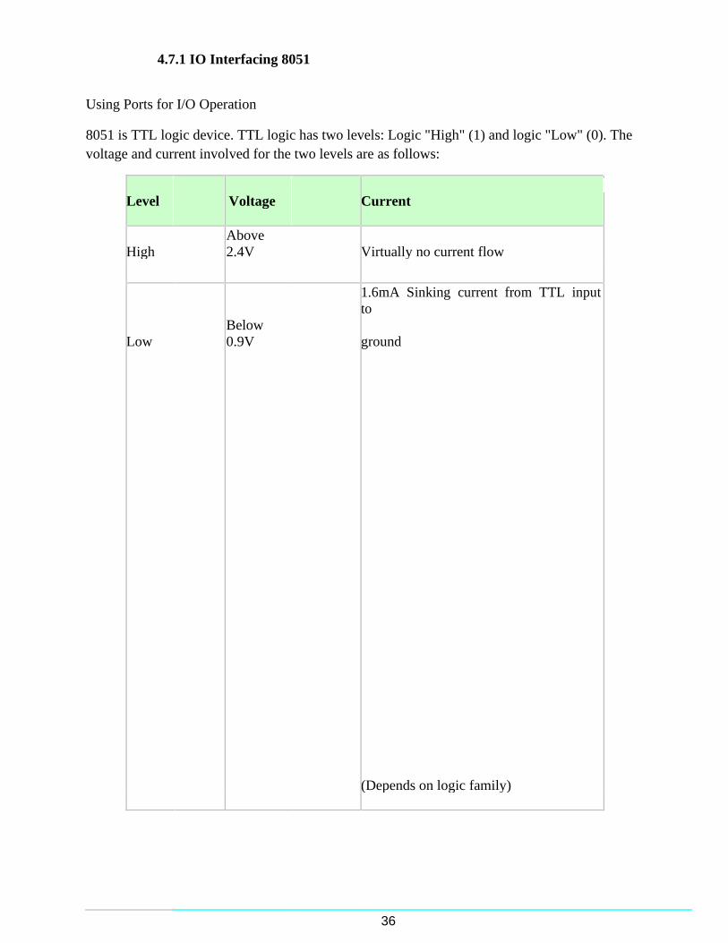
36
4.7.1 IO Interfacing 8051
Using Ports for I/O Operation 8051 is TTL logic device. TTL logic has two levels: Logic "High" (1) and logic "Low" (0). The
voltage and current involved for the two levels are as follows:
Level
Voltage
Current
High
Above
2.4V Virtually no current flow
1.6mA Sinking current from TTL input
to
Low
Below
0.9V ground
(Depends on logic family)

37
Ports Function
Port 0 Dual-purpose port- 1. general purpose I/O Port.
(Pin 32-39) 2. multiplexed address & data bus
Open drain outputs
Port 1
(Pin 1-8)
Dedicated I/O port – Used solely for interfacing to external devices
Internal pull-ups
Port 2
Dual-purpose
port- 1. general purpose I/O port.
(Pin 21-28) 2. a multiplexed address & data bus.
Internal pull-ups
Port 3
(Pin 10-
17)
Dual-purpose port- 1. general purpose I/O port.
2. pins have alternate purpose related to
special features of the 8051
Internal pull-ups

38
4.7.2Port functions The 8051 internal ports are partly bi-directional (Quasi-bi-directional). The following is the internal
circuitry for the 8051 port pins:
Figure 4.13 Diagram
4.7.3Configuring for output P0 is open drain. – Has to be pulled high by external 10K resistors. – Not needed if P0 is used for address lines Writing to a port pin loads data into a port latch that drives a FET connected to the port pin. P0: Note that the pull-up is absent on Port 0 except when functioning as the external address/data bus.
When a "0" is written to a bit in port 0, the pin is pulled low. But when a "1" is written to it, it is in
high impedance (disconnected) state. So when using port 0 for output, an external pull-up resistor is
needed, depending on the input characteristics of the device driven by the port pin P1, P2, P3 have internal pull-ups: When a "0" is written to a bit in these port , the pin is pulled low (
FET-ON) ,also when 1 is written to a bit in these port pin becomes high (FET-OFF) thus using port
P1,P2,P3 is simple. 4.7.4 . Configuring for input At power-on all are output ports by default To configure any port for input, write all 1’s (0xFF) to the port
Latch bit=1, FET=OFF, Read Pin asserted by read instruction
You can used a port for output any time. But for input, the FET must be off. Otherwise, you will be
reading your own latch rather than the signal coming from the outside. Therefore, a "1" should be
written to the pin if you want to use it as input, especially when you have used it for output before. If
you don't do this input high voltage will get grounded through FET so you will read pin as low and not
as high. An external device cannot easily drive it high so, you should not tide a port high directly without any resistor. Otherwise, the FET would burn.
Be Careful :

39
Some port pins serve multiple functions. Be careful writing to such ports. For example, P3.0 is the
UART RXD (serial input), and P3.1 is the UART TXD (serial output). If you set P3.0 to a '0', an
external buffer (such as an RS232 level translator) cannot drive it high. Therefore you have prevented
receiving any serial input. If an external interrupt such as EX1 on P3.3 is enabled, and set to be level sensitive, and you clear this
pin's output latch to a zero, guess what? You've just caused a perpetual interrupt 1. The pin's input
buffer will read the output of it's latch as always low. Your controller will spend all of its time in the
interrupt handler code and will appear to have crashed, since it will have very little time for other
tasks. In fact, it will get to execute a single instruction before re-entering the interrupt handler, so the
rest of your program will execute very, very slowly. 4.7.5 Switch On I/O Ports
Figure 4.14 Switch circuits
It is always best connecting the switch to ground with a pull-up resistor as shown in the "Good"
circuit. When the switch is open, the 10k resistor supplies very small current needed for logic 1. When
it is closed, the port pin is short to ground. The voltage is 0V and all the sinking current requirement is
met, so it is logic 0. The 10k resistor will pass 0.5 mA (5 Volt/10k ohm). Thus the circuits waste very
little current in either state. The drawback is that the closure of switch gives logic 0 and people like to
think of a switch closure gives logic 1. But this is not a matter because it is easy to handle in software. The "Fair" circuit requires that the pull-down resistor be very small. Otherwise, the pin will rise above
0.9V when the resistor passes the 1.6mA sinking current. When the switch is closed, the circuit waste
a large current since virtually no current flows into the pin. The only advantage is that a switch closure
gives logic 1.
In the "Poor" circuit, the logic 1 is stable when the switch is closed. But when the switch is open, the
input floats to a noise-sensitive high rather than a low. An open TTL pin is usually read as logic 1 but
the pin may picks up noise like an antenna. To conclude, driving a TTL input should always consider current sinking (pulling input to 0V).

40
4.7.6 Led On I/O Ports Figure 7.3 IO Ports Since TTL outputs is designed to feed multiple TTL inputs, they are good at current sinking but poor
at current sourcing. The Standard TTL can sink up to 16mA and source 250uA. The LS logic family
can sink 8mA and source 100uA. The 8051 port pin can sink 1.6mA (3.2mA for port 0) and source
60uA. Therefore, if you drive significant current, try to arrange your circuits to use current sinking. Unlike diodes, Light-emitting diodes have a forward voltage drop from 1.7 to 2.5 volts and most of
them flow a forward current 20mA. since the TTL output can't source above 1mA so the LED will be very dim.
The resistor limits the current. The resistance can be calculated by assuming its voltage is about 2.5V
and the TTL output is 0.9V. For 2.2V LED, 1.9V is across the resistor so the 220ohm would limit the
current to 8.6mA (1.9/220). For 1.7V LED, 2.4V is across the resistor so it would limit the current to
10.9mA (2.4/220). The resistor should not less than 100ohm or the LED would fail.

41
4.7.6 LED Circuits: Fig 4.6 Interfacing Diagram
Figure 4.15 LED Circuits
Connection -Port 1 is connected to eight LEDs, each of them is connected to 5V through a 330ohm
resistor. Port 0 is connected to a DIP switch and a 10Kohm resistor Condition - Corresponding led should light up when switch pressed , i.e. if Switch at 1.0 is pressed - >
LED at P0.0 should light up.
Reference Books:
1. Kennith J. Ayala, 8051 Microcontroller, Thomson, 2005.
2. A.NagoorKani, Microprocessor & Microcontroller, Tata Mc Graw Hill, 3«Edition, 2012
3. B. Ram, Fundamentals of Microprocessors and Microcomputers, Dhanpat Rai Publications, 2001

1
SCHOOL OF BIO AND CHEMICAL ENGINNEERING
DEPARTMENT OF BIOMEDICAL ENGINEERING
UNIT -5
Application of microprocessors: Stepper Motor Control, Temperature control, TTL to RS232
Conversion RS232 to TTL Conversion - Interfacing EPROMs & SRAMs with 8085. Interfacing
Biosignal to Microprocessor- block diagram.
Fundamentals of Microprocessor and Microcontroller – SEC1323

2
5.1. Interfacing ADC to 8051
ADC (Analog to digital converter) forms a very essential part in many embedded projects and
this article is about interfacing an ADC to 8051 embedded controller. ADC 0804 is the ADC
used here and before going through the interfacing procedure, we must neatly understand how
the ADC 0804 works.
5.1.1 ADC 0804.
ADC0804 is an 8 bit successive approximation analogue to digital converter from National
semiconductors. The features of ADC0804 are differential analogue voltage inputs, 0-5V input
voltage range, no zero adjustment, built in clock generator, reference voltage can be externally
adjusted to convert smaller analogue voltage span to 8 bit resolution etc. The pin out diagram of
ADC0804 is shown in the figure below.
Figure 5.1 Pin Diagarm
The voltage at Vref/2 (pin9) of ADC0804 can be externally adjusted to convert smaller input
voltage spans to full 8 bit resolution. Vref/2 (pin9) left open means input voltage span is 0-5V
and step size is 5/255=19.6V. Have a look at the table below for different Vref/2 voltages and
corresponding analogue input voltage spans.
Vref/2 (pin9) (volts) Input voltage span (volts) Step size (mV)

3
Left open 0 – 5 5/255 = 19.6
2 0 – 4 4/255 = 15.69
1.5 0 – 3 3/255 = 11.76
1.28 0 – 2.56 2.56/255 = 10.04
1.0 0 – 2 2/255 = 7.84
0.5 0 – 1 1/255 = 3.92
Steps for converting the analogue input and reading the output from ADC0804.
1 Make CS=0 and send a low to high pulse to WR pin to start the conversion. 2 Now keep checking the INTR pin. INTR will be 1 if conversion is not finished and INTR
will be 0 if conversion is finished. 3 If conversion is not finished (INTR=1) , poll until it is finished. 4 If conversion is finished (INTR=0), go to the next step. 5 Make CS=0 and send a high to low pulse to RD pin to read the data from the ADC.
5.1.2 Circuit diagram.

4
Figure 5.2 : Interfacing of ADC The figure above shows the schematic for interfacing ADC0804 to 8051. The circuit initiates the
ADC to convert a given analogue input , then accepts the corresponding digital data and displays
it on the LED array connected at P0. For example, if the analogue input voltage Vin is 5V then
all LEDs will glow indicating 11111111 in binary which is the equivalent of 255 in decimal.
AT89s51 is the microcontroller used here. Data out pins (D0 to D7) of the ADC0804 are
connected to the port pins P1.0 to P1.7 respectively. LEDs D1 to D8 are connected to the port
pins P0.0 to P0.7 respectively. Resistors R1 to R8 are current limiting resistors. In simple words
P1 of the microcontroller is the input port and P0 is the output port. Control signals for the ADC
(INTR, WR, RD and CS) are available at port pins P3.4 to P3.7 respectively. Resistor R9 and
capacitor C1 are associated with the internal clock circuitry of the ADC. Preset resistor R10
forms a voltage divider which can be used to apply a particular input analogue voltage to the
ADC. Push button S1, resistor R11 and capacitor C4 forms a debouncing reset mechanism.
Crystal X1 and capacitors C2,C3 are associated with the clock circuitry of the microcontroller.

5
5.1.3 Program.
ORG 00H MOV P1,#11111111B // initiates P1 as the input port
MAIN: CLR P3.7 // makes CS=0
SETB P3.6 // makes RD high
CLR P3.5 // makes WR low
SETB P3.5 // low to high pulse to WR for starting conversion
WAIT: JB P3.4,WAIT // polls until INTR=0
CLR P3.7 // ensures CS=0
CLR P3.6 // high to low pulse to RD for reading the data from ADC
MOV A,P1 // moves the digital data to accumulator
CPL A // complements the digital data (*see the notes)
MOV P0,A // outputs the data to P0 for the LEDs
SJMP MAIN // jumps back to the MAIN program
END
5.2 Interfacing of DAC 8085/8051
Microcontroller are used in wide varietyof applications like for measuring and control of physical
quantitylike temperature, pressure, speed, distance, etc.
In these systems microcontroller generates output which is in digital form but the controlling
system requires analog signal as they don't accept digital data thus making it necessary to use DAC
which

6
In the figure shown, we use-bit8 DAC 0808. This IC converts digital data into equivalent analog
Current.Hence we require an I to V converter to convertthis
current into equivalent voltage.
According to theory of DAC Equivalent analog output is given as: Ex:
1. IF data =00H [00000000], Vref=
10
V
Therefore, V0= 0 Volts.
2. If data is 80H [10000000], Vref= 10V
Therefore, V0= 5 Volts.
Different Analog output voltages for different Digital signal is given as:

7
5.2.2 Interfacing Diagram
Figure 5.3 DAC Interfacing
5.3.Stepper Motor Interfacing With 8085/8051

8
Figure 5.4 Stepper Motor Interfacing A stepper motor is a device that translates electrical pulses into mechanical movement. The
stepper motor rotates in steps in response to the applied signals. It is used in applications such as disk drives,
dot matrix printers, plotters and robotics.It is mainly used for position control. Stepper motors have a
permanent magnet called rotor (also called the shaft) surrounded by a stator . There are also steppers called
variable reluctance stepper motors that do not have a PM rotor. The most common stepper motors have
four stator windings that are paired with a center-tapped. This type of stepper motor is commonly referred
to as a. four-phase or unipolar stepper motor. The center tap allows a change of current direction in each
of two coils when a winding is grounded, thereby resulting in a polarity change of the stator.
5.4.TTL to RS232 Conversion
The TTL-RS232 Adapter is used to connect TTL level signals to an RS-232 interface. The TTL
side is a 9-pin female connector and the RS -232 side is a 9-pin male connector. The unit can
be powered through one of the connector pins or through the side mounted power jack. The TTL side has a voltage suppression network designed to protect against ESD and EFT. The unit can be powered by supplying 5-24VDC on pin 5 of the TTL connector or through the
side mounted power jack.
TTL Signal Pin Signal Name RS232 Signal Pin
1 (Input) TXD 3 (Output)
2 (Output) RXD 2 (Input)
3 (Input) RTS 7 (Output)

9
4 Ground 5
5 (5-24VDC) PWR 4 (See Warning)
Figure 5.5: TTL to RS232 Conversion
6 (Output) CD 1 (Input)
7,8,9 No Connection
6, 8 ,9

10
Grid Connect has a TTL to Ethernet product that has a TTL interface. This TTL-RS232
Adapter can be connected to the TTL-Ethernet Adapter so that an RS232 source can be used
to setup and configure the TTL-ETH Adapter. The following cable diagram shows how to
make a cable to connect a TTL-RS232 Adapter to a TTL-Ethernet Adapter.
Cable between TTL-232 and TTL-ETH DB9 Male DB9 Female
TXD -1 TXD -4 TO Male
DB-
TO Female DB-9 RXD-2 RXD-5 9
on TTL-232 RTS-3 RTS-9
on TTL-
ETH
Adapter GND-4 GND-2 Adapter
DCD-
6 DCD-3

11
5.5.RS232-TTL
The MAX232 is an integrated circuit first created in 1987 by Maxim Integrated Products that
converts signals from a TIA-232 (RS-232) serial port to signals suitable for use in TTL-
compatible digital logic circuits. The MAX232 is a dual driver/receiver and typically converts
the RX, TX, CTS and RTS signals. The drivers provide TIA-232 voltage level outputs (about ±7.5 volts) from a single 5-volt supply
by on-chip charge pumps and externalcapacitors. This makes it useful for implementing TIA-232
in devices that otherwise do not need any other voltages. The receivers reduce TIA-232 inputs, which may be as high as ±25 volts, to standard 5-volt TTL
levels. These receivers have a typical threshold of 1.3 volts and a typical hysteresis of 0.5 volts.
Versions
The later MAX232A is forward compatible with the original MAX232 but may operate at higher
baud rates and can use smaller external capacitors – 0.1 μF in place of the 1.0 μF capacitors used
with the original device.[1] The newer MAX3232 is also backwards compatible, but operates at a
broader voltage range, from 3 to 5.5 V.[2] Pin-to-pin compatible versions from other manufacturers are ICL232, SP232, ST232, ADM232
and HIN232. Texas Instruments makes compatible chips, using MAX232 as the part number. Voltage levels
It is helpful to understand what occurs to the voltage levels. When a MAX232 IC receives a TTL
level to convert, it changes a TTL logic 0 to between +3 and +15 V, and changes TTL logic 1 to
between −3 and −15 V, and vice versa for converting from TIA-232 to TTL. This can be
confusing when you realize that the TIA-232 data transmission voltages at a certain logic state
are opposite from the TIA-232 control line voltages at the same logic state. To clarify the matter,
see the table below. For more information, see RS-232 voltage levels.
TIA-232 line type and logic level
TIA-232
voltage
TTL voltage to/from
MAX232
Data transmission (Rx/Tx) logic 0 +3 V to +15 V 0 V

12
Data transmission (Rx/Tx) logic 1
−3 V to −15 V
5 V
Control signals (RTS/CTS/DTR/DSR)
logic 0 −3 V to −15 V 5 V
Control signals (RTS/CTS/DTR/DSR)
logic 1 +3 V to +15 V 0 V
Applications:
RS-232 to TTL converters that use MAX232: The MAX232(A) has two receivers that convert
from RS-232 to TTL voltage levels, and two drivers that convert from TTL logic to RS-232
voltage levels. As a result, only two out of all RS-232 signals can be converted in each direction.
Typically, the first driver/receiver pair of the MAX232 is used for TX and RX signals, and the
second one for CTS and RTS signals.There are not enough drivers/receivers in the MAX232 to
also connect the DTR, DSR, and DCD signals. Usually, these signals can be omitted when, for
example, communicating with a PC's serial interface. If the DTE really requires these signals,
either a second MAX232 is needed, or some other IC from the MAX232 family can be used. Also,
it is possible to connect DTR (DE-9 pin #4) directly to DSR (DE-9 pin #6) without going through
any circuitry, which provides an automatic (brain-dead) DSR acknowledgment of the incoming
DTR signal.The MAX232 family was subsequently extended by Maxim to versions with four
receivers and transmitters (the MAX238) and a version with eight receivers and transmitters (the
MAX248), as well as several other combinations of receivers and transmitters.

13
5.6.Interfacing EPROM & SRAM
8031 chip is a ROMless version of the 8051. In other words, it is exactly like any member of the
8051 family such as the 8751 or 89C51 as far as executing the instructions and features are
concerned, but it has no on-chip ROM. Therefore, to make the 8031 execute 8051 code, it must
be connected to external ROM memory containing the program code. In this section we look at
interfacing the 8031 microcontroller with external ROM. Before we discuss this topic, one might
wonder why someone would want to use the 8031 when they could buy an 8751, 89C51, or
DS5000. The reason is that all these chips have a limited amount of on-chip ROM. Therefore, in
many systems where the on-chip ROM of the 8051 is not sufficient, the use of an 8031 is ideal
since it allows the program size to be as large as 64K bytes. Although the 8031 chip itself is
much cheaper than other family members, an 8031-based system is much more expensive since
the ROM containing the program code is connected externally and requires more supporting
circuitry, as we explain next. EA pin To indicate that the program code is stored in external ROM, this pin must be connected to
GND. This is the case for the 8051-based system. In fact, there are times when, due to repeated
burning and erasing of on-chip ROM, its UV-EPROM is no longer working. In such cases one
can also use the 8751 (or 89C51 or any 8051) as the 8031. All we have to do is to connect the
EA pin to ground and connect the chip to external ROM containing the program code.PO and P2
role in providing addresses

14
Figure 5.6 D Flip Flop Since the PC (program counter) of the 8031/51 is 16-bit, it is capable of accessing up to 64K
bytes of program code. In the 8031/51, port 0 and port 2 provide the 16-bit address to access
external memory. Of these two ports, PO provides the lower 8 bit addresses AO – A7, and P2
provides the upper 8 bit addresses A8 – A15. More importantly, PO is also used to provide the 8-
bit data bus DO – D7. In other words, pins PO.O – P0.7 are used for both the address and data
paths. This is called address/data multiplexing in chip design. Of course the reason Intel used
address/data multiplexing in the 8031/51 is to save pins. How do we know when PO is used for
the data path and when it is used for the address path? This is the job of the ALE (address latch
enable) pin. ALE is an output pin for the 8031/51 microcontroller. Therefore, when ALE = 0 the
8031 uses PO for the data path, and when ALE = 1, it uses it for the address path. As a result, to
extract the addresses from the PO pins we connect PO to a 74LS373 latch (see Figure 14-8) and
use the ALE pin to latch the address as shown in Figure 14-9. This extracting of addresses from
PO is called address/data demultiplexing.

15
Figure 5.7 Address/Data Multiplexing From Figure 14-9, it is important to note that normally ALE = 0, and PO is used as a data bus,
sending data out or bringing data in. Whenever the 8031/51 wants to use PO as an address bus, it
puts the addresses AO – A7 on the PO pins and activates ALE = 1 to indicate that PO has the
addresses.
Figure 5.8 Data, Address and Control Buses for the 8051/8085
PSEN:
Another important signal for the 8031/51 is the PSEN (program store enable) signal. PSEN is an
output signal for the 8031/51 microcontroller and must be connected to the OE pin of a ROM
containing the program code. In other words, to access external ROM containing program code,
the 8031/51 uses the PSEN signal. It is important to emphasize the role of EA and PSEN when

16
connecting the 8031/51 to external ROM. When the EA pin is connected to GND, the 8031/51
fetches opcode from external ROM by using PSEN. Notice in Figure 14-11 the connection of the
PSEN pin to the OE pin of ROM. In systems based on the 8751/89C51/DS5000 where EA is
connected to VCC, these chips do not activate the PSEN pin. This indicates that the on-chip
ROM contains program code. In systems where the external ROM contains the program code, burning the program into ROM
leaves the microcontroller chip untouched. This is preferable in some applications due to
flexibility. In such applications the software is updated via the serial or parallel ports of the IBM
PC. This is especially the case during software development and this method is widely used in
many 8051-based trainers and emulators.
Figure 5.9 Interfacing of Memory
Reference Books:
1.Ramesh S Gaonkar, Microprocessor Architecture, Programming and application with 8085, 4»
Edition, Penram International Publishing, New Delhi, 2000
2. Kennith J. Ayala, 8051 Microcontroller, Thomson, 2005.
3. Dougles V. Hall, Microprocessor and Interfacing, Tata MC Graw Hill Publication, 2.‹Edition,
1992.
4. Charless M. Gilmore, “Microprocessor Principle and application, McGraw Hill publication,
1995.
5. A.NagoorKani, Microprocessor & Microcontroller, Tata Mc Graw Hill, 3«Edition, 2012
6. B. Ram, Fundamentals of Microprocessors and Microcomputers, Dhanpat Rai Publications,
2001 .