sc8915 high efficiency, synchronous, bi directional buck boost … · charge converter with i2c...
TRANSCRIPT

SC8915 DATASHEET
SOUTHCHIP SEMICONDUCTOR SOUTHCHIP CONFIDENTIAL
Copyright © 2017, Southchip Semiconductor Technology (Shanghai) Co., Ltd.
SC8915 High Efficiency, Synchronous, Bi-Directional Buck-Boost Charge Converter with I2C Interface
1 Description
SC8915 is a synchronous buck-boost Li-ion battery
charger which also supports reverse discharging
operation. It integrates two power MOSFETs and can
support up to 36V battery voltage and up to 26V VBUS.
It can be used to effectively manage the charging
process for 1~6 cell Li-ion batteries no matter adapter
voltage is higher, lower or equal to the battery voltage.
When a system needs to generate an output from the
battery, SC8915 can also discharges the cells and
delivers desired output no matter it is higher, lower or
equal to the battery voltage.
Through its I2C interface, user can set the charging /
discharging mode easily, and program the charging
current, charging voltage, reserve output voltage,
current limits, switching frequency and other
parameters flexibly. Besides that, SC8915 integrates
10-bit ADC, so user can read the VBUS / VBAT voltage
and current in real time, simplifying the system design.
SC8915 supports internal current limit, over voltage
protection, output short protection and over temperature
protections to ensure safety under different abnormal
conditions.
SC8915 adopts 40 pin QFN 6x6 package.
2 Features
• Buck-Boost Battery Charger for 1 to 6 Cell Batteries
• Charging Management including Trickle Charge,
CC Charge, CV Charge and Charge Termination
• Buck-Boost Reverse Discharging Mode
• Integrates Two Power MOSFETs
• Wide VBAT Range: 2.5 V to 36 V, 40V sustainable
• Wide VBUS Range: 2.5 V to 26 V, 30V sustainable
• I2C Programmable Charging Current and Voltage
• I2C Programmable Discharging Output Voltage
• I2C Programmable Input / Output Current Limit
• I2C Programmable Switching Frequency
• High Efficiency Buck-Boost Conversion
• 10-bit ADC resources
• Charging Status Indication
• Event Detections, including Automatic Adapter
Insert and Automatic Load Insert Detection
• Power Path Control
• Under Voltage Protection, Over Voltage Protection,
Over Current Protection, Short Circuit Protection
and Thermal Shutdown Protection
• QFN-40 Package
3 Applications
• Power Bank
• USB Power Delivery
• Type C Hub
• Industrial Power Supplies
4 Device Information
Part Number Package Dimension
SC8915QDHR 40 pin QFN 6.0mm x 6.0mm x 0.75mm

SC8915 DATASHEET
SOUTHCHIP SEMICONDUCTOR SOUTHCHIP CONFIDENTIAL
Copyright © 2017, Southchip Semiconductor Technology (Shanghai) Co., Ltd. 2
5 Typical Application Circuit
VBUS
FB
VBATV
BA
TS
AG
ND
CO
MP
PS
TO
P
SC
L
HD
1
SN
S1
N
SN
S1
P
VCC
BT2
LD2
SW2
PG
ND
SNS2N
SNS2P
HD2S
W1
VBUS VBAT
+
OTG = 0, charging
OTG = 1, discharging
SD
A
INT
VB
US
P
HG
BT
1
LD
1
LG
GPO
PGATE
ACIN
VDD
USB_A
AC adapter /
Micro USB
AD
IN
CP
Host
Control
INDET
VDRV
*NOTE: It takes time for MCU to write the I2C
register to control the PGATE signal. If fast turn on/
off for this PMOS is required like for short circuit
protection, it is recommended to use MCU to control
this PMOS directly.
* NOTE

SC8915 DATASHEET
SOUTHCHIP SEMICONDUCTOR SOUTHCHIP CONFIDENTIAL
Copyright © 2017, Southchip Semiconductor Technology (Shanghai) Co., Ltd. 3
6 Terminal Configuration and Functions
SC8915 Top View
40 39 38 37 36 35 34
65
43
21
7
PGND
8
33
BT
1
SW
1
HG
VB
US
VB
US
P
SW
1
HD
1
VCC
PGND
LD2
PGND
SN
S2
P
VBAT
PGND
SN
S2N
FB
AG
ND
CO
MP
AD
IN
INT
91
0
32 31
11 12 13 14 15 16 17 18 19 20
25
26
27
28
29
30
24
23
22
21
VBUSP
VBUSP
SNS1N
SNS1P
GPO
CP
PGATE/DITHER
INDET
ACIN
SC
L
SD
A
VDRV
SW
1
LD
1
LG
42
SW1
43
PGND
41
VBUSP
PSTOP
VB
AT
S
BT2
HD2
SW2
TERMINAL
I/O DESCRIPTION
NUMBER NAME
1, 2, 40 VBUSP I/O Power node of VBUS. Connect to adapter input port or USB port. Work as the power input of the
converter when in charging mode, and power output in discharging mode.
3 SNS1N I Negative input of a current sense amplifier. Connect to one pad of the current sense resistor (typical 10 mΩ) on the power path to sense the current into or out from VBUS.
4 SNS1P I Positive input of a current sense amplifier. Connect to one pad of the current sense resistor (typical 10 mΩ) on the power path to sense the current into or out from VBUS.
5 GPO O Open drain output for general purpose. It is controlled by GPO_CTRL bit. User can use this pin to
drive external PMOS with a pull up resistor.
6 CP O
Driver for external charge pump circuit. (CHARGE PUMP NOT RECOMMENDED. It is
suggested to leave this pin floating, and connect VDRV with VCC. Consult local FAE if charge pump is needed)
7 PGATE/DITHER IO
PMOS gate driver controlled by PGATE bit, used to control the external PMOS on the power
path. This pin can be configured through I2C for switching frequency dithering function. Connect a ceramic capacitor (typical 100nF) from this pin to ground when for frequency dither function.
8 INDET I Connect this pin to a USB-A port to detect the load insertion event. When an insertion event is

SC8915 DATASHEET
SOUTHCHIP SEMICONDUCTOR SOUTHCHIP CONFIDENTIAL
Copyright © 2017, Southchip Semiconductor Technology (Shanghai) Co., Ltd. 4
detected, the IC sets INDET bit and outputs an INT interrupt pulse to inform MCU.
9 ACIN I
Connect this pin to AC adapter input node or micro-USB port to detect an AC adapter insertion
event. When an insertion event is detected, the IC sets AC_OK bit and outputs an INT interrupt pulse to inform MCU.
10 PSTOP I
Power stop control. Pull this pin to logic low to enable the power blocks; pull this pin to logic high to disabled the power blocks, and the IC enters into Standby mode. In Standby mode, only the AC adapter and load insert detection functions and the I2C circuits keep working.
This pin is internally pulled low.
11 SCL I I2C interface clock. Connect SCL to the logic rail through a pull up resistor (typical 10 kΩ). The IC works as a slave, and the I2C address is 0x74H.
12 SDA I/O I2C interface data. Connect SDA to the logic rail through a pull up resistor (typical 10 kΩ).
13 INT O An open drain output for interrupt signal. The IC sends a logic low pulse at INT pin to inform the host if an interrupt event happens.
14 AGND I/O Analog ground. Connect PGND and AGND together at the thermal pad under IC.
15 ADIN I ADC input pin. Apply an analog signal (≤ 2.048V) to this pin, the internal 10-bit ADC can convert
this analog signal to digital signals, and store the digital values in a register.
16 FB I Feedback node for VBUS voltage. Connect a resistor divider from VBUS to FB to set the VBUS discharging output voltage in external way. The FB reference can also be programmed through
I2C.
17 COMP I Connect resistor and capacitor at this pin to compensate the control loop.
18 VBATS I Sense node for VBAT voltage. Connect to VBAT rail if internal way is selected for VBAT charging
termination voltage setting; connect a resistor divider at VBATS if external way is selected.
19 SNS2N I Negative input of a current sense amplifier. Connect to one pad of the current sense resistor (typical 10 mΩ) on the power path to sense the current into or out from battery.
20 SNS2P I Positive input of a current sense amplifier. Connect to the other pad of the current sense resistor (typical 10 mΩ) on the power path to sense the current into or out from battery.
21 VBAT I Power supply to the IC. Connect to the battery positive node. Place a 1 μF capacitor from this pin to PGND as close to the IC as possible.
22 BT2 I Connect a 100nF capacitor between BT2 pin and SW2 pin to bootstrap a bias voltage for high
side MOSFET driver.
23 HD2 O Gate driver output to control the external high side power MOSFET.
24-26 PGND I/O Power ground. Connect PGND and AGND together at the PGND thermal pad under IC.
27 SW2 I/O Switching node. Connect to the inductor.
28 LD2 O Gate driver output to control the external low side power MOSFET.
29 VCC O Output of an internal 5V linear regulator. Connect a 1 μF capacitor from VCC pin to PGND as close to the IC as possible.
30 VDRV I
Power supply input for internal driver circuits. One way of getting the power supply is to connect VCC to this pin directly. Another way is to use the CP driver to implement a charge pump between VCC and VDRV pin. (CHARGE PUMP WAY IS NOT RECOMMENDED. CONSULT
LOCAL FAE IF CHARGE PUMP IS USED)

SC8915 DATASHEET
SOUTHCHIP SEMICONDUCTOR SOUTHCHIP CONFIDENTIAL
Copyright © 2017, Southchip Semiconductor Technology (Shanghai) Co., Ltd. 5
31 LG I Gate input of the integrated low side MOSFET. Connect to LD1 pin with or without a driving resistor in between.
32 LD1 O Gate driver output to the integrated low side MOSFET. User can short LD1 pin and LG pin directly, or connect a driving resistor between LD1 and LG pins to limit the driver current.
33 – 35 SW1 I/O Switching Node. Connect to the inductor.
36 HD1 O Gate driver output to the integrated high side MOSFET. User can short HD1 pin and HG pin directly, or connect a driving resistor between HD and HG pins to limit the driver current.
37 HG I Gate input of the integrated high side MOSFET. Connect to HD1 pin with or without a driving resistor in between.
38 BT1 I Connect a 100nF capacitor between BT1 pin and SW1 pins to bootstrap a bias voltage for high
side MOSFET driver.
39 VBUS I Power supply to the IC. Connect to the VBUS rail. Place a 1 μF capacitor from this pin to PGND
as close to the IC as possible.
41 VBUSP I/O VBUSP thermal pad under IC. Connect to VBUSP pins together.
42 SW1 I/O Switching thermal pad under IC. Connect to SW1 pins together.
43 PGND I/O PGND thermal pad under IC. Connect to PGND pins together. Connect AGND and PGND together at this thermal pad.

SC8915 DATASHEET
SOUTHCHIP SEMICONDUCTOR SOUTHCHIP CONFIDENTIAL
Copyright © 2017, Southchip Semiconductor Technology (Shanghai) Co., Ltd. 6
7 Specifications
7.1 Absolute Maximum Ratings
over operating free-air temperature range (unless otherwise noted) (1)
MIN MAX Unit
Voltage range at terminals(2)
CP, VCC, VDRV, LD1, LD2, LG,
HD1 to SW1, HG to SW1, BT1 to SW1, BT2 to SW2, HD2 to SW2 -0.3 6.5 V
PSTOP -0.3 6 V
SCL, SDA, INT, ADIN, COMP -0.3 5 V
VBUSP, SNS1N, SNS1P, FB, SW1 -0.3 30 V
VBUS to SNS1P, SNS1N -0.3 11 V
VBAT to SNS2P, SNS2N -0.3 11 V
SNS1P to SNS1N -10 10 V
SNS2P to SNS2N -10 10 V
HD1,BT1 -0.3 35 V
GPO, PGATE, INDET, ACIN, VBATS, SNS2N, SNS2P, VBAT, SW2 -0.3 40 V
HD2, BT2 -0.3 45 V
BT1 to HD1, BT2 to HD2 -0.3 6.5 V
TJ Operating junction temperature range -40 150 °C
Tstg Storage temperature range -65 150 °C
(1) Stresses beyond those listed under absolute maximum ratings may cause permanent damage to the device. These are stress ratings only, and functional operation of the device at these or any other conditions beyond those indicated under recommended operating conditions is not implied. Exposure to absolute-maximum-rated conditions for extended periods may affect device reliability.
(2) All voltage values are with respect to network ground terminal.
7.2 Thermal Information
THERMAL RESISTANCE(1) QFN-40 (6mmX6mm) UNIT
θJA Junction to ambient thermal resistance 58 °C/W
θJC Junction to case resistance 5 °C/W
(1) Measured on JESD51-7, 4-layer PCB.
7.3 Handling Ratings
PARAMETER DEFINITION MIN MAX UNIT
ESD(1) Human body model (HBM) ESD stress voltage(2) -2 2 kV
Charged device model (CDM) ESD stress voltage(3) -750 750 V
(1) Electrostatic discharge (ESD) to measure device sensitivity and immunity to damage caused by assembly line electrostatic discharges into the device.
(2) Level listed above is the passing level per ANSI, ESDA, and JEDEC JS-001. JEDEC document JEP155 states that 500-V HBM allows safe manufacturing with a standard ESD control process.
(3) Level listed above is the passing level per EIA-JEDEC JESD22-C101. JEDEC document JEP157 states that 250-V CDM allows safe manufacturing with a standard ESD control process.
7.4 Recommended Operating Conditions
MIN MAX UNIT

SC8915 DATASHEET
SOUTHCHIP SEMICONDUCTOR SOUTHCHIP CONFIDENTIAL
Copyright © 2017, Southchip Semiconductor Technology (Shanghai) Co., Ltd. 7
VBUS VBUS voltage range 2.7 26 V
VBAT VBAT voltage range 2.6 36 V
CBUS, CBAT Bulk capacitor for VBUS/VBAT (effective value) 30 µF
L Inductance 2.2 10 µH
RSNS1/2 Current Sensing Resistor 5 10 mΩ
TA Operating ambient temperature -40 85 C
TJ Operating junction temperature -40 125 C

SC8915 DATASHEET
SOUTHCHIP SEMICONDUCTOR SOUTHCHIP CONFIDENTIAL
Copyright © 2017, Southchip Semiconductor Technology (Shanghai) Co., Ltd. 8
7.5 Electrical Characteristics
TJ= 25°C and VBUS = 5V, VBAT = 10.8V unless otherwise noted.
PARAMETER TEST CONDITIONS MIN TYP MAX UNIT
SUPPLY VOLTAGE
VUVLO_VBUS VBUS under-voltage lockout threshold
Rising edge 2.5 2.7 V
Hysteresis 170 mV
VUVLO_VBAT VBAT under-voltage lockout
threshold
Rising edge 2.4 2.6 V
Hysteresis 170 mV
IQ_VBAT Quiescent current into VBAT
VBUS = 5V
PSTOP = L, non-switching 2.4 4 mA
VBUS = 5V
PSTOP = L, after charging termination
2.4 4 mA
IQ_VBUS Quiescent current into VBUS PSTOP = L, non-switching 25 40 μA
ISB_VBAT Standby current into VBAT
VBUS open
PSTOP = H, AD_START = 0 17 40 μA
VBUS open
PSTOP = H, AD_START = 1 0.65 1.2 mA
ISB_VBUS Standby current into VBUS PSTOP = H, AD_START = 0 12 50 μA
VCC, DIRVER AND POWER SWITCH
VCC VCC regulation voltage
PSTOP = L, VBUS = 9V 5.0 5.3 V
PSTOP = L, VBUS = 5V 4.96 5 V
PSTOP = H, VBAT=3.6V 3 V
IVCC_LIM VCC current limit
PSTOP = L
VBUS = 5V, VCC = 4.5V 17 25 30 mA
PSTOP = L
VBUS = 9V, VCC = 4.5V 160 mA
PSTOP = H 1 mA
VDRV VDRV regulation voltage
change pump connected
VBUS = 5V, IDRV = 0mA 5.8 6.2 6.5 V
change pump connected
VBUS = 9V, IDRV = 30mA 5.7 6.1 6.4 V
RHS/LS_PU High/low side MOS driver pull up resistor
4 Ω
RHS/LS_PD High/low side MOS driver pull
down resistor 1 Ω
RDSon_HS High side MOS on resistance VDRV = 6V 9 10 mΩ
RDSon_LS Low side MOS on resistance VDRV = 6V 9 10 mΩ
REFERENCE VOLTAGE IN CHARGING MODE
VBATS_ext VBATS reference voltage for external setting
VBAT_SEL = 1 1.197 1.203 1.209 V
VBATS_int VBATS accuracy for internal
setting, over VBATS target
VBAT_SEL = 0, CSEL = 00
VCELL_SET=000~111 -0.5 0.5 %
VTRICKLE_int Trickle charge threshold voltage
for internal setting
VBAT_SEL = 0, Cell number = N
VCELL_SET = 000~1111,
TRICKLE_SET = 0
2.73*N 2.94*N 3.15*N V

SC8915 DATASHEET
SOUTHCHIP SEMICONDUCTOR SOUTHCHIP CONFIDENTIAL
Copyright © 2017, Southchip Semiconductor Technology (Shanghai) Co., Ltd. 9
VBAT_SEL = 0, Cell number = N
VCELL_SET = 000~1111,
TRICKLE_SET = 1
2.31*N 2.52*N 2.73*N V
VTRICKLE_ext Trickle charge threshold for external setting, over VBAT target
VBAT_SEL = 1,
TRICKLE_SET = 0 65 70 75 %
VBAT_SEL = 1,
TRICKLE_SET = 1 55 60 65 %
VEOC EOC voltage threshold, over VBAT target
VBAT_SEL = 0/1 97% 98% 99%
VRECH Recharge threshold voltage, over VBAT target
VBAT_SEL = 0/1 94.8% 95.8% 96.8%
VINREG VINREG reference voltage
4.5V target
VINREG_SET = 0x2C, VINREG_RATIO = 0
4.3 4.5 4.7 V
15V target
VINREG_SET = 0x95, VINREG_RATIO = 0
14.7 15 15.3 V
4.48V target
VINREG_SET = 0x6F, VINREG_RATIO = 1
4.4 4.5 4.6 V
10V target
VINREG_SET = 0xF9, VINREG_RATIO = 1
9.8 10 10.2 V
VBAT_OVP VBAT OVP threshold, over VBAT target
VBAT_SEL = 0/1 103% 105.5% 108%
VCLAMP 125 mV
REFERENCE VOLTAGE IN DISCHARGING MODE
VFB FB reference voltage for external
setting
FB_SEL = 1, VBUSREF_E_REF
target from 0.5V to 2.048V -2% 2%
VBUS VBUS reference voltage accuracy
for internal setting
FB_SEL = 0
VBUS_RATIO = 1 (5x)
VBUS = 3.6 ~10.24V
-2% 2%
FB_SEL = 0
VBUS_RATIO = 0 (12.5x)
VBUS = 9 ~ 24V
-2% 2%
VBUS_OVP
VBUS OVP threshold, rising edge VBUSREF_I_SET = 1V
VBUSREF_E_SET = 1V 107.3% 110% 113%
Hysteresis VBUSREF_I_SET = 1V
VBUSREF_E_SET = 1V 3%
CURRENT LIMIT
IBUS_LIM IBUS current limit accuracy
Charging mode, 6A target
IBUS_RATIO = 01 (6x)
IBUS_LIM = 0x7F
-10% 10%
Charging mode, 3A target
IBUS_RATIO = 10 (3x)
IBUS_LIM = 0x7F
-10% 10%
Discharging mode, 6A target
IBUS_RATIO = 01 (6x)
IBUS_LIM = 0x7F
-10% 10%
Discharging mode, 3A target
IBUS_RATIO = 10 (3x) -10% 10%

SC8915 DATASHEET
SOUTHCHIP SEMICONDUCTOR SOUTHCHIP CONFIDENTIAL
Copyright © 2017, Southchip Semiconductor Technology (Shanghai) Co., Ltd. 10
IBUS_LIM = 0x7F
IBAT_LIM IBAT current limit accuracy
Charging mode, 6A target
IBAT_RATIO = 0 (6x)
IBAT_LIM = 0xFF
-10% 10%
Charging mode, 12A target
IBAT_RATIO = 1 (12x)
IBAT_LIM = 0xFF
-10% 10%
Discharging mode, 6A target
IBAT_RATIO = 0 (6x)
IBAT_LIM = 0xFF
-15% 15%
Discharging mode, 12A target
IBAT_RATIO = 1 (12x)
IBAT_LIM = 0xFF
-15% 15%
ITRICKLE
Trickle charge current, over IBAT_LIM setting
10%
Trickle charge current, over IBUS_LIM setting
22%
IEOC EOC current threshold, over IBUS_LIM / IBAT_LIM setting
EOC_SET= 0 4%
EOC_SET= 1 10%
ERROR AMPLIFIER
GmEA Error amplifier gm 0.12 0.15 0.18 mS
ROUT Error amplifier output resistance (1) 20 MΩ
ISINK_COMP COMP sink current LOOP_SET = 0/1 25 μA
ISRC_COMP COMP source current LOOP_SET = 0 18 μA
LOOP_SET = 1 32 μA
IBIAS_FB FB pin input bias current FB_SEL = 1
FB in regulation 50 nA
SWITCHING
fSW Switching frequency
FREQ_SET = 00 (150kHz) 140 155 170 kHz
FREQ_SET = 01 (300kHz) 270 305 330 kHz
FREQ_SET = 11 (450kHz) 400 450 500 kHz
POWER PATH MANAGEMENT
RPU_PGATE PGATE pin pull up resistor EN_PGATE = 0 20 kΩ
RPD_PGATE PGATE pin pull down resistor EN_PGATE = 1 6 kΩ
VCLAMP Clamp voltage from VBUS to PGATE pin
EN_PGATE = 1 6.9 7.35 7.7 V
RRD_GPO GPO pin pull down resistor GPO_CTRL = 1 6 kΩ
DETECTION
VAC_DET AC detection threshold 2.9 3.1 3.4 V
VSHORT Short circuit detection threshold 0.95 1 1.05 V
I2C AND LOGIC CONTROL
RPD PSTOP pin internal pull down
resistor 0.75 1 1.25 MΩ
VIL PSTOP, SCL, SDA input low voltage
0.4 V
VIH PSTOP, SCL, SDA input high voltage
1.2 V

SC8915 DATASHEET
SOUTHCHIP SEMICONDUCTOR SOUTHCHIP CONFIDENTIAL
Copyright © 2017, Southchip Semiconductor Technology (Shanghai) Co., Ltd. 11
ISINK_INT INT pin sink current VINT = 0.4V 0.3 0.375 0.45 mA
ISINK_SCL/SDA SCL/SDA pin sink current VSCL/SDA = 0.4V 100 mA
tPULSE Interrupt pulse width (logic low) 0.6 1 1.5 ms
SOFTSTART
tdeglitch Deglitch time for charging
PSTOP = L, OTG_SET = 0
VBUS = 5V, from PSTOP low to IC
starting charging
220 ms
tSS Internal soft-start time
VBUS from 0V to 5V in discharging mode
VBUS_Ratio = 1 (5x)
12 ms
THERMAL SHUTDOWN
TSD
Thermal shutdown temperature (1) 165 °C
Thermal shutdown hysteresis (1) 15 °C

SC8915 DATASHEET
SOUTHCHIP SEMICONDUCTOR SOUTHCHIP CONFIDENTIAL
Copyright © 2017, Southchip Semiconductor Technology (Shanghai) Co., Ltd. 12
8 Detailed Description
8.1 Charging Mode
Charging mode and discharging mode is selected by EN_OTG bit.
When EN_OTG bit is 0, the IC works in charging mode. The current flows from VBUS to VBAT to charge the battery cells.
When in charging mode, the IC charges the battery cells according to below typical charging profile. When battery voltage is lower than trickle charge threshold, the IC charges the cells with small charging current; when cell voltage is higher than the threshold, the IC enters into Constant Current charging phase, and charges the cells with constant current set by IBUS limit or IBAT limit. When the cell voltage reaches the termination voltage target, the IC enters into Constant Voltage charge phase, and charges the cells with gradually decreased current until the current is lower than termination current threshold. Once termination voltage and termination current conditions are satisfied, the IC enters into End of Charge phase. In this phase the IC can either terminate the charging or keep charging the cells.
Termination voltage
CC (constant
current) charge
Trickle charge current
Termination current
Trickle charge
threshold
EOC indication
Trickle chargeCC (constant
current) charge
CV (constant
voltage) charge
Recharge-threshold
End of
chargerecharge
Figure 1 Typical Charging Profile
8.1.1 Trickle Charge
The trickle charge voltage threshold can be set to 60% or 70% of 4.2V/cell by TRICKLE_SET bit. When in trickle charge phase, the charging current is reduced to a small value for the good of battery cells. If ICHAR_SEL bit is 0, the IBUS is reduced to 22% of the IBUS current limit set value; if ICHAR_SEL bit is 1, the IBAT is reduced to 10% of IBAT current limit set value.
If trickle charging phase is not needed, the user can set DIS_TRICKLE bit to 1 to disable it.
8.1.2 CC Charge (Constant Current Charge)
When cell voltage is higher than the trickle threshold, the IC charges the battery cells with constant current set by IBUS limit or IBAT limit, which are set respectively through IBUS_LIM_SET and IBAT_LIM_SET registers. The current limit value can be changed dynamically, and is also related to the current sense resistor and ratio bits. Please see Register Map section for details.
In charging mode, the IC regulates the current which reaches its current limit value first. For example, if IBUS current limit
is set to 3A, IBAT limit is set to 10A, and when IBUS reaches 3A, IBAT is only 6A, which is much lower than IBAT limit 10A, then the IC limits the IBUS at 3A.
It is not allowed to set any of the current limits to 0A. Keep the minimum current limit above 0.3A.
8.1.3 CV Charge (Constant Voltage Charge)
The battery target voltage can be set internally, by CSEL bits and VCELL_SET bits. The CSEL bits set the battery cell numbers connected in series, and VCELL_SET bits set the battery voltage per cell. For example, if the battery cells are in xp2s connection (several cells are connected in parallel, and two cells in series) and the cell voltage is 4.3V, the user should set CSEL to 01 (2S), and set VCELL_SET bits to 011 (4.3V).
When the battery charging voltage is set internally, the user should connect VBATS pin to VBAT terminal to sense the battery voltage, and the VBAT_SEL bit should be set to 0.
If VBAT_SEL is set to 1, it means the battery voltage is set externally. Under this condition, the user should use resistor divider at VBATS pin to set the target voltage as below. VCELL_SET and CSEL bits don’t work. The reference voltage of VBATS is 1.2V.
VBAT = VBATS_REF× (1+RUP
RDOWN)
VBAT
VBATS
VBAT
VBATS
+
A. VBAT_SEL = 0
B. VBAT_SEL = 1
Rup
Rdown
+
Figure 2 Battery voltage setting
When the battery cell voltage reaches 98% of the cell target voltage, the IC enters into CV charge phase. In this phase, the VBAT voltage is regulated at target value, and the charging current reduces gradually.
8.1.4 EOC (End of Charge)
When both of below voltage condition and current condition for EOC detection are satisfied, the IC enters into EOC phase, and informs the MCU through EOC interrupt bit.
1. the cell voltage is higher than 98% of set value

SC8915 DATASHEET
SOUTHCHIP SEMICONDUCTOR SOUTHCHIP CONFIDENTIAL
Copyright © 2017, Southchip Semiconductor Technology (Shanghai) Co., Ltd. 13
2. the IBUS or IBAT current (decided by ICHAR_SEL bit) is
lower than 1/10 or 1/25 (decided by EOC_SET bit) of its
current limit value
In EOC phase, the IC can terminate the charging process or keep charging the battery cells, which can be set by DIS_TERM bit. If IC keeps charging, it regulates the battery cell voltage at set value.
8.1.5 Recharge
If the IC terminates the charging process after EOC is detected, the battery voltage may drop slowly due to leakage or operation current from battery cells. Once the VBAT voltage drops below 95% of the set voltage, the EOC bit is cleared, and the IC enters into CC charge phase and recharges the battery.
8.1.6 Self-adaptive Charging Current (VINREG)
The IC features dynamic power management. The allowed minimum VBUS operation voltage is VINREG threshold, which can be set by VINREG_SET register and VINREG_RATIO bit dynamically. During charging, if the IBUS charging current is higher than adapter’s current capability, the adapter will be overloaded and the VBUS voltage is pulled low. Once the IC detects the VBUS voltage drops at VINREG threshold, it reduces the charging current automatically and regulates the VBUS voltage at VINREG threshold.
8.1.7 Battery Impedance Compensation
The IC provides the function of battery impedance compensation. User can set the impedance through IRCOMP bits, then the VBAT target voltage in CV phase is compensated as
VBAT_cmp = VBAT_set + min(IBAT∙IRCOMP, VCLAMP)
Where,
VBAT_cmp is the compensated battery voltage target; VBAT_set is the originally set battery termination target; IBAT is the charging current at battery side; IRCOMP is the resistance compensation value set by IRCOMP bits; VCLAMP is the allowed maximum compensation value, fixed at 125mV.
User should carefully evaluate the real battery impedance. If the
value set by IRCOMP bits is higher than the real value, it will cause over charge.
8.2 Discharging Mode
When EN_OTG bit is set to1, the IC enters into discharging mode. In discharging mode, the battery (VBAT) is discharged and the current flows from VBAT to VBUS.
If FB_SEL is set to 0, the VBUS output voltage is set internally, through VBUSREF_I_SET and VBUSREF_I_SET2 registers and the VBUS_RATIO bit. The VBUS can be changed dynamically, and the recommended VBUS voltage range is from 3.5V to 25.6V. When VBUS is lower than 10.24V, it is suggested to set the VBUS_RATIO to 5x, and so
the minimum changing step is 10mV/step; when VBUS is higher than 10.24V, VBUS_RATIO should be set to 12.5x, and the minimum changing step is 25mV/step.
If FB_SEL is set to 1, the VBUS voltage target is set externally, that is, by the resistor divider connected at FB pin, and can be calculated as below.
VBUS = VBUSREF_E x (1+RUP
RDOWM)
Even if VBUS is set externally, the user can still change the VBUS voltage dynamically by changing the reference voltage VBUSREF_E through VBUSREF_E_SET and VBUSREF_E_SET2 registers. The default VBUSREF_E is 1V, and recommended VBUSREF_E voltage range is from 0.7V to 2.048V.
Please see Register Map section for details.
The IBUS current limit and IBAT current limit are still functional in discharging mode and can be changed dynamically.
It is not allowed to set any of the current limits to 0A. Keep the minimum current limit above 0.3A.
8.2.1 Soft Start
The IC integrates soft-start control to generate VBUS voltage in discharging mode. When VBUS is lower than VSHORT (typ. 1V), both IBUS and IBAT current limits are fold back to 1/10 of the setting value. Meanwhile, the IC ramps up the internal reference voltage gradually (~10ms) to avoid inrush current.
If there is a load at VBUS at the beginning of the startup, the IC may fail to boost the VBUS voltage beyond VSHORT due to the 1/10 current limits for both IBUS and IBAT. If startup with loading is required, user shall set the DIS_ShortFoldBack bit to 1 to disable the current limit fold back function. After startup, the user can set DIS_ShortFoldBack bit back to 0, so to enable this function for short circuit protection. See VBUS Short Protection section for details.
8.2.2 Slew Rate Setting
When the VBUS voltage is changed dynamically through reference voltage (VBUSREF_I_SET and VBUSREF_I_SET2 registers or VBUSREF_E_SET and VBUSREF_E_SET2 registers), the reference voltage change rate can be controlled through SLEW_SET bits. For example, the VBUS is set in internal way with 5x ratio, and the VBUSREF_I = 1V at first (VBUS = 5V), then the user sets the VBUSREF_I voltage to 1.6V to get 8V output. If the slew rate is 2mV/ μs, the VBUS voltage will increase to 8V in 600mV / 2mV/μs = 300μs.
8.2.3 PFM Operation
The IC supports PFM operation in discharging mode by setting EN_PFM bit to 1. In PWM mode, the IC always works with constant switching frequency for the whole load range. This helps achieve the best output voltage performance, but the efficiency is low at light load condition because of the high switching loss.

SC8915 DATASHEET
SOUTHCHIP SEMICONDUCTOR SOUTHCHIP CONFIDENTIAL
Copyright © 2017, Southchip Semiconductor Technology (Shanghai) Co., Ltd. 14
In PFM mode, the IC still works with constant switching frequency under heavy load condition, but under light load condition, the IC automatically changes to pulse frequency modulation operation to reduce the switching loss. The efficiency can be improved under light load condition while output voltage ripple will be a little larger compared with PWM operation. Below figure shows the output voltage behavior of PFM mode.
Normal VOUT
PFM operation at light load
Change to PWM operation at heavy load
Vout
PFM VOUT
Figure 3 PFM mode illustration
8.3 ADC for Voltage and Current Monitor
The IC integrates a 10-bit ADC, so the IC can monitor the VBUS/VBAT voltages and IBUS/IBAT current no matter in charging mode or discharging mode. Besides these, the IC provides an analog input: ADIN pin for 10-bit ADC sampling. The maximum voltage the ADC can sample at ADIN pin is 2.048V, and the sampling resolution is 2mV/step. The ADC function is enabled after AD_START bit is set to 1. When ADC is enabled in standby mode, the IC will 0.5mA~1mA operation current. Please see Register Map section for details.
8.4 Power Path Management
The IC offers power path management function at PGATE and GPO pins. The PGATE pin can be used to drive PMOS connected at VBUS. The PGATE pin is connected to a 6 kΩ pull down resistor internally when EN_PGATE is set to 1, and the maximum voltage between VBUS and PGATE is clamped at 7.35V; when EN_PGATE is set to 0, PGATE pin is connected to VBUS rail through a 20 kΩ pull up resistor internally
The GPO pin is an open drain output, so external pull up resistor is needed. When GPO_CTRL bit is set to 0, GPO outputs high impedance; when GPO_CTRL is set to1, GPO is pulled down internally and the pull down resistance is 6 kΩ.
User can use PGATE pin and GPO pin to control the isolation MOSFETs between adapter input and USB output as shown in Typical Application Circuit.. However, the MCU or system controller controls the bits through I2C interface, which takes time for communication, so the PMOS may not be turned on/off very quickly. In the application where the isolation PMOS needs to be controlled very fast, it is suggested to use the I/O pins of MCU to control the PMOS on/off directly.
8.5 Phone Insert Detection
If connecting INDET pin to USB-A port as shown in Typical Application Circuit , the IC can detect the phone detection.
Once the IC detects a phone is inserted, it sets the INDET interrupt bit to inform MCU. The INDET bit is cleared after it is read by MCU.
8.6 Adapter Attachment / Detachment
Detection
If connecting ACIN pin to Micro-USB port as shown in Typical Application Circuit. the IC can detect the attachment / detachment of the adapter.
Once the ACIN pin voltage is higher than 3V, which means the adapter is inserted, the IC sets the AC_OK interrupt bit to inform MCU about the attachment. If the ACIN pin voltage is lower than 3V, which means the adapter is removed, the IC clears AC_OK bit to inform the MCU about the detachment.
8.7 Switching and Frequency Dithering
The IC switches in fixed frequency which can be adjusted through FREQ_SET bits. The switching dead time can also be set through DT_SET pins. Please see Register Map section for details.
The IC also offers frequency dithering function. This function can be enabled by setting EN_DITHER bit to 1. When the function is enabled, the switching frequency is not fixed, but varies within +/- 5% range. For example, if the switching frequency is set to 300kHz (FREQ_SET = 01), the frequency will change from 285kHz to 315kHz gradually and then back to 285kHz back and forth. The time it varies from the lowest to the highest frequency or from highest to lowest frequency can be controlled by a capacitor connected at PGATE/DITHER pin as below equation shows. For example, if 100nF capacitor is connected, the time is 1.2 ms.
T_dither = 120 mV × C
10 μA
When EN_DITHER is set to 1, the PGATE driver function is disabled, and the PGATE/DITHER pin only operates for dithering function.
8.8 VCC Regulator and Driver Supply
The IC integrates a regulator and generates a 5V voltage at VCC pin with typically 25 mA driving capability. The regulator is powered by the higher voltage of VBUS or VBAT.
When in Standby mode (PSTOP is pulled high), the VCC regulator is shutdown, so VCC voltage is reduced and has very limited current capability. It is not suggested to use VCC in Standby mode.
The internal driving circuit is powered from VDRV pin, and user should provide a supply at VDRV pin to power the circuit. The user can connect VCC to VDRV directly, or connect an external power supply to VDRV. Besides the two ways, the IC offers a charge pump driver at CP pin, which can pump the VCC voltage to power VDRV pin. With charge pump circuit, the IC can regulate the VDRV voltage. at 6V.
Charge pump is not recommended for VDRV. Consult local FAE
if charge pump is used.

SC8915 DATASHEET
SOUTHCHIP SEMICONDUCTOR SOUTHCHIP CONFIDENTIAL
Copyright © 2017, Southchip Semiconductor Technology (Shanghai) Co., Ltd. 15
VCC CP VDRV
VCC CP VDRV
VCC CP VDRV
External supply
(<6.5V)
A. connect VC to VDRV directly
(HIGHLY RECOMMENDED)
B. Use charge pump to power VDRV
(NOT RECOMMEND)
B. Use external power supply
VDRV = 6VVCC = 5V
VCC = 5V
VCC = 5V
Figure 4 Supply for VDRV
8.9 Standby Mode
When PSTOP signal is high, the IC enters into Standby mode. In this mode, the IC stops switching to save the quiescent current. The other functions are still valid, and the MCU can still control the IC through I2C. However, if ADC function is enabled in Standby mode, the quiescent current will be increased to 0.5mA~1mA.
8.10 Protection
8.10.1 VBUS Over Voltage Protection
User can enabled / disable VBUS over voltage protection in discharging mode by DIS_OVP bit. When OVP is enabled, the IC stops switching when VBUS is higher than the target voltage by 10%.
8.10.2 VBAT Over Voltage Protection
The IC implements VBAT over voltage protection in both
charging mode and discharging mode. Once the VBAT voltage is higher than target voltage by 10%, the IC stops switching.
8.10.3 VBUS Short Protection
In discharging mode, if the VBUS voltage is detected lower than VSHORT (typ. 1V), the IC sets the VBUS_SHORT interrupt bit to inform the MCU. In the same time, the IBUS current limiting value and IBAT current limiting value were reduced to 22% and 10% of setting value respectively to protect the IC. If DIS_ShortFoldBack bit is set to 1, the IBUS and IBAT current limit will not be reduced.
8.10.4 Over Temperature Protection
When the IC detects the junction temperature is higher than 165°C, the IC stops switching to protect the chip, and sets the OTP interrupt bit to inform the MCU. It resumes switching once the temperature drops below 15°C.
8.11 I2C and Interrupt
8.11.1 I2C Interface
The IC features I2C interface, so the MCU or controller can control the IC flexibly. The 7-bit I2C address of the chip is 0x74 (8-bit address is 0xE8 for write command, 0xE9 for read command). The SDA and SCL pins are open drain and must be connected to the positive supply voltage via a current source or pull-up resistor. When the bus is free, both lines are HIGH. The I2C interface supports both standard mode (up to 100kbits) and fast mode (up to 400k bits with 5 kΩ pull up resistor at SCL pin and SDA pin respectively).
8.11.1.1 Data Validity
The data on the SDA line must be stable during the HIGH period of the clock. The HIGH or LOW state of the data line can only change when the clock signal on the SCL line is LOW. One clock pulse is generated for each data bit transferred.
Figure 5 Bit transfer on the I2C bus
8.11.1.2 START and STOP Conditions
All transactions begin with a START (S) and are terminated by a STOP (P). A HIGH to LOW transition on the SDA line while SCL is HIGH defines a START condition. A LOW to HIGH transition on the SDA line while SCL is HIGH defines a STOP condition.
START and STOP conditions are always generated by the master. The bus is considered to be busy after the START

SC8915 DATASHEET
SOUTHCHIP SEMICONDUCTOR SOUTHCHIP CONFIDENTIAL
Copyright © 2017, Southchip Semiconductor Technology (Shanghai) Co., Ltd. 16
condition. The bus is considered to be free again a certain time after the STOP condition.
Figure 6 START and STOP conditions
8.11.1.3 Byte Format
Every byte put on the SDA line must be eight bits long. The number of bytes that can be transmitted per transfer is unrestricted. Each byte must be followed by an Acknowledge bit. Data is transferred with the Most Significant Bit (MSB) first. If a slave cannot receive or transmit another complete byte of data until it has performed some other function, for example servicing an internal interrupt, it can hold the clock line SCL LOW to force the master into a wait state. Data transfer then continues when the slave is ready for another byte of data and releases clock line SCL.
Figure 7 Data transfer on the I2C bus
8.11.1.4 Acknowledge (ACK) and Not Acknowledge
(NACK)
The acknowledge takes place after every byte. The acknowledge bit allows the receiver to signal the transmitter that the byte was successfully received and another byte may be sent. During data is transferred, the master can either be the transmitter or the receiver. No matter what it is, the master generates all clock pulses, including the acknowledge ninth clock pulse.
The transmitter releases the SDA line during the acknowledge clock pulse so the receiver can pull the SDA line LOW and it remains stable LOW during the HIGH period of this clock pulse.
When SDA remains HIGH during this ninth clock pulse, this is defined as the Not Acknowledge signal. The master can then generate either a STOP condition to abort the transfer, or a repeated START condition to start a new transfer.
8.11.1.5 The slave address and R/W bit
Data transfers follow the format shown in below. After the START condition (S), a slave address is sent. This address is seven bits long followed by an eighth bit which is a data direction bit (R/W) — a ‘zero’ indicates a transmission (WRITE), a ‘one’ indicates a request for data (READ). A data transfer is always terminated by a STOP condition (P) generated by the master. However, if a master still wishes to communicate on the bus, it can generate a repeated START condition (Sr) and address another slave without first
generating a STOP condition.
Figure 8 A complete data transfer
Figure 9 The first byte after the START procedure
8.11.1.6 Single Read and Write
Figure 10 Single Wite
Figure 11 Single Read
If the register address is not defined, the charger IC send back NACK and go back to the idle state.
8.11.1.7 Multi-Read and Multi-Write
The IC supports multi-read and multi-write for continuous registers.
Figure 12 Multi-Write
Figure 13 Multi-Read

SC8915 DATASHEET
SOUTHCHIP SEMICONDUCTOR SOUTHCHIP CONFIDENTIAL
Copyright © 2017, Southchip Semiconductor Technology (Shanghai) Co., Ltd. 17
8.11.2 Interrupt
When AC_OK/VBUS_SHORT/OTP/EOC is set to 1, or clear to 0, the IC sends an interrupt pulse as below at INT pin to inform MCU. But when INDET only is set to 1, the IC sends an interrupt pulse. It is summarized as below:
Status Signal Interrupt Triggering Mechanism
Reserved
AC_OK Rising edge or falling edge triggers 1ms_pulse INT
INDET2 Only rising edge triggers 1ms_pulse INT
INDET1 Only rising edge triggers 1ms_pulse INT
VBUS_SHORT Logic high triggers continuous INT
OTP Rising edge or falling edge triggers 1ms_pulse INT
EOC Rising edge or falling edge triggers 1ms_pulse INT
Reserved
The interrupt pulse at INT pin is as follow:
1msINT
Figure 14 Interrupt pulse at INT pin
The INDET bit is read and clear type. Except INDET, all other bits in Status register represent the real time status. User can mask the interrupt output of any bit by setting its corresponding bit in Mask register. When the mask bit is set, the corresponding status bit is still set, but the IC doesn’t send the interrupt at INT pin.

SC8915 DATASHEET
SOUTHCHIP SEMICONDUCTOR SOUTHCHIP CONFIDENTIAL
Copyright © 2017, Southchip Semiconductor Technology (Shanghai) Co., Ltd. 18
9 Application Information
9.1 Capacitor Selection
The switching frequency of the IC is in the range of 150kHz ~ 450kHz. Since MLCC ceramic capacitor has good high frequency filtering with low ESR, above 60µF X5R or X7R capacitors with higher voltage rating then operating voltage with margin is recommended. For example, if the highest operating Vin/Vout voltage is 12V, select at least 16V capacitor and to secure enough margin, 25V voltage rating capacitor is recommended.
The high capacitance polymer capacitor or tantalum capacitor can be used for input and output but capacitor voltage rating must be higher than the highest operating voltage with enough margin. The high frequency characteristics of these capacitors are not as good as ceramic capacitor, so at least 10µF ceramic capacitor should be placed in parallel to reduce high frequency ripple.
9.2 Inductor Selection
2.2 μH to 4.7 μH inductor is recommended for loop stability. The peak inductor current in discharging mode can be calculated as
IL_peak = IBAT + VBAT∙(VBUS-VBAT∙η)
2∙fsw∙L∙VBUS (VBUS≥VBAT)
IL_peak = IBUS + VBUS∙(VBAT - VBUS)
2∙fsw∙L∙VBAT∙η (VBUS<VBAT)
where IBAT is the battery current at VBAT side, and can be calculated as
IBAT = VBUS∙IBUS
η∙VBAT
𝜂 is the power conversion efficiency. User can use 90% for calculation.
fsw is the switching frequency
L is the inductor value
The peak inductor current in charging mode can be calculated as
IL_peak = IBAT + VBAT∙(VBUS-VBAT)
2∙fsw∙L∙VBUS∙η (VBUS>VBAT)
IL_peak = IBUS + VBUS∙(VBAT-VBUS∙η)
2∙fsw∙L∙VBAT (VBUS≤VBAT)
where IBAT is the battery charging current at VBAT side, and can be calculated as
IBAT = VBUS∙IBUS∙η
VBAT
𝜂 is the power conversion efficiency. User can use 90% for calculation.
fsw is the switching frequency
L is the inductor value
When selecting inductor, the inductor saturation current must be higher than the peak inductor current with enough margin (20% margin is recommended). The rating current of the inductor must be higher than the battery current.
The inductor DC resistance value (DCR) affects the conduction loss of switching regulator, so low DCR inductor is recommended especially for high power application. The conductor loss of inductor can be calculated roughly as
PL_DC = IL2∙DCR
IL is the average value of inductor current, and it equals to IBAT or IBUS.
Besides DC power loss, there are also inductor AC winding loss and inductor core loss, which are related to inductor peak current. Normally, higher peak current causes higher AC loss and core loss. The user can consult with the inductor vendor to select the inductors which have small ESR at high frequency and small core loss.
9.3 Current Sense Resistor
The RSNS1 and RSNS2 are current sense resistors. 10 mΩ should be used for RSNS1 to sense IBUS current, 5 mΩ or 10 mΩ used for RSNS2 to sense IBAT current (10 mΩ supports higher battery current limit accuracy, and 5 mΩ supports higher efficiency). Resistor of 1% or higher accuracy and low temperature coefficient is recommended.
Note: If the user wants to use other resistor values, please contact factory for support.
The resistor power rating and temperature coefficient should be considered. The power dissipation is roughly calculated as P=I2R, and I is the highest current flowing through the resistor. The resistor power rating should be higher than the calculated value.
Normally the resistor value is varied if the temperature increased and the variation is decided by temperature coefficient. If high accuracy of current limit is required, select lower temperature coefficient resistor as much as possible.
9.4 MOSFET Selection
The IC integrates two power MOSFETs, and the user should add two external power MOSFETs at VBAT side.
The VDS of MOSFET should be higher than the highest operating voltage with enough margin (recommend more than 10V higher). For example, if the highest operating voltage is 20V, at least 30V rated VDS MOSFET should be selected; If the highest operating voltage is 24V, 40V VDS voltage rating should be selected.
The VGS voltage rating of MOSFET should be selected higher than 8V. Considering PCB parasitic parameters during operation, MOSFET VGS voltage might be higher than
VDRV voltage due to transient overshoot, so 10V VGS is
recommended to secure sufficient margin.
The MOSFET current ID should be higher than the highest
SC8915 DATASHEET
SOUTHCHIP SEMICONDUCTOR SOUTHCHIP CONFIDENTIAL
Copyright © 2017, Southchip Semiconductor Technology (Shanghai) Co., Ltd. 19
battery current with enough margin.
To ensure the sufficient current capability in relatively high
temperature circumstance, the current rate at TA=70˚C or TC
= 100˚C should be considered. In addition, the power
dissipation value PD should also be considered and higher PD is better in applications. Make sure that MOSFET power consumption must not exceed PD value.
The MOSFET RDS(ON) and input capacitor CISS impact power efficiency directly. Typically, lower RDS(ON) MOSFET has higher CISS. The RDS(ON) is related to conduction loss. Higher RDSON results in higher conduction loss, thus lower efficiency and higher thermal dissipation; the CISS is related to MOSFET switch on/off time, and longer on/off time results in higher switching loss and lower efficiency. The proper MOSEFT should be selected based on tradeoff between the RDS(ON) and CISS.
If high CISS MOSFET is selected, the switching on and off time become longer, then the dead time should be adjusted to avoid simultaneous turn on for both high side and low side MOSFETs.
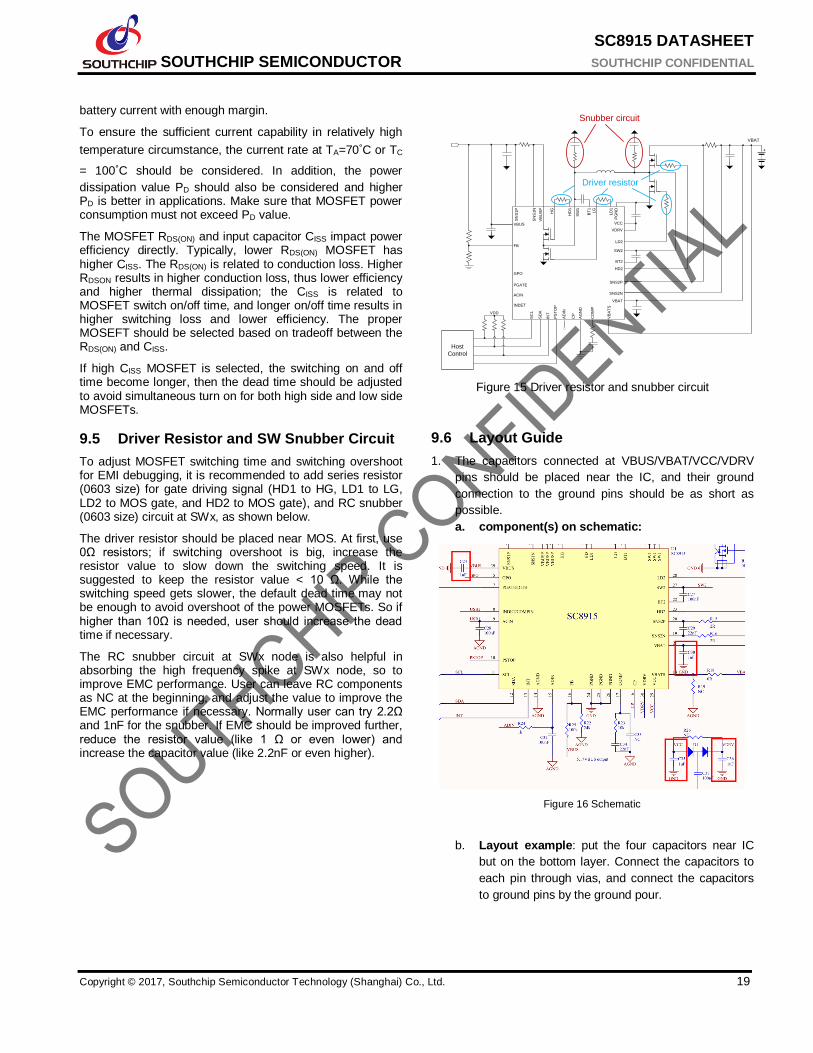
9.5 Driver Resistor and SW Snubber Circuit
To adjust MOSFET switching time and switching overshoot for EMI debugging, it is recommended to add series resistor (0603 size) for gate driving signal (HD1 to HG, LD1 to LG, LD2 to MOS gate, and HD2 to MOS gate), and RC snubber (0603 size) circuit at SWx, as shown below.
The driver resistor should be placed near MOS. At first, use 0Ω resistors; if switching overshoot is big, increase the resistor value to slow down the switching speed. It is suggested to keep the resistor value < 10 Ω. While the switching speed gets slower, the default dead time may not be enough to avoid overshoot of the power MOSFETs. So if higher than 10Ω is needed, user should increase the dead time if necessary.
The RC snubber circuit at SWx node is also helpful in absorbing the high frequency spike at SWx node, so to improve EMC performance. User can leave RC components as NC at the beginning, and adjust the value to improve the EMC performance if necessary. Normally user can try 2.2Ω and 1nF for the snubber. If EMC should be improved further, reduce the resistor value (like 1 Ω or even lower) and increase the capacitor value (like 2.2nF or even higher).
VBUS
FB
VBAT
VB
AT
S
AG
ND
CO
MP
PS
TO
P
SC
L
HD
1
SN
S1
N
SN
S1
P
VCC
BT2
LD2
SW2
PG
ND
SNS2N
SNS2P
HD2
SW
1
Snubber circuit
VBAT
+
SD
A
INT
VB
US
P
HG
BT
1
LD
1
LG
GPO
PGATE
ACIN
VDD
AD
IN
CP
Host
Control
INDET
VDRV
Driver resistor
Figure 15 Driver resistor and snubber circuit
9.6 Layout Guide
1. The capacitors connected at VBUS/VBAT/VCC/VDRV
pins should be placed near the IC, and their ground
connection to the ground pins should be as short as
possible.
a. component(s) on schematic:
Figure 16 Schematic
b. Layout example: put the four capacitors near IC
but on the bottom layer. Connect the capacitors to
each pin through vias, and connect the capacitors
to ground pins by the ground pour.

SC8915 DATASHEET
SOUTHCHIP SEMICONDUCTOR SOUTHCHIP CONFIDENTIAL
Copyright © 2017, Southchip Semiconductor Technology (Shanghai) Co., Ltd. 20
Figure 17 Bottom layer (flip view)
Figure 18 Top layer (flip view)
2. Between IBUS current sense resistor and VBUSP pins,
add a 100nF 0402 capacitor to PGND. It is helpful to
suppress high frequency noise. Put it very close to
VBUSP pins and PGND pins.
a. component(s) on schematic
Figure 19 Schematic
b. Layout example: the capacitor is put on the bottom
of the IC, just from the VBUSP pad to PGND pad.
Figure 20 Bottom layer (flip view)
3. Put IBUS current sense resistor and bulk capacitor at
VBUS side should be placed very close to VBUSP pins
and PGND pins.
a. component(s) on schematic

SC8915 DATASHEET
SOUTHCHIP SEMICONDUCTOR SOUTHCHIP CONFIDENTIAL
Copyright © 2017, Southchip Semiconductor Technology (Shanghai) Co., Ltd. 21
Figure 21 Schematic
b. Layout example: put the current sense resistor just
near the IC on the top layer, and connect to the
bulk capacitors through wide copper on the top
layer. The bulk capacitors are connected to PGND
pins through vias and ground pour on the bottom
layer. Keep the ground pour as wide as possible.
Figure 22 Top layer view
Figure 23 Bottom layer view
4. Put IBAT current sense resistor, MOSFETs and bulk
capacitor at VBAT side as close as possible. And the
low side MOSFET and bulk capacitors should be very
close to PGND pins. Between current sense resistor
and high side MOS, add a 100nF 0402 capacitor to
PGND. It is helpful to suppress high frequency noise.
Put it very close to MOS and PGND pins.
a. component(s) on schematic
Figure 24 Schematic
b. Layout example: put all these components on the
top layer as a group, and the VBAT and PGND
power paths should be as wide as possible. The
low side MOS, 100nF capacitor and the bulk
capacitors connected to PGND pins through ground
pour on both top layer and bottom layer.
Figure 25 Top layer view

SC8915 DATASHEET
SOUTHCHIP SEMICONDUCTOR SOUTHCHIP CONFIDENTIAL
Copyright © 2017, Southchip Semiconductor Technology (Shanghai) Co., Ltd. 22
Figure 26 Bottom layer view
5. The driver signals (LD2 / HD2 / SW2) as shown below
should be routed with wide traces (≥ 15 mil). The driver
resistors should be placed near MOS. The HD2 and
SW2 should be routed in parallel, close to each other;
the LD2 should be routed in parallel with PGND traces
(≥ 15 mil) or close to PGND pour. There should be wide
space filled with PGND between LD2 and HD2 and also
wide space from LD2 to SW2 to avoid interference.
Figure 27 Schematic
6. The current sense traces should be connected to the
current sense resistor’s pads in Kelvin sense way as
below, and routed in parallel (differential routing), and
add filter for each current sense near the IC.
Must connect to resistor pads
(Kevin Sense)Should NOT connect to coppers of
power path
correct wrong
RSNSx RSNSx
copper copper copper copper
Figure 28 Current sense
a. component(s) on schematic
Figure 29 Schematic
b. Layout example: since the R1 should be put near
the IC, so the filter components and traces for
sense are also placed near the IC. The space for
routing is limited, so the resistors of the filter are put
on the bottom layer. The current sense resistor R2
should be placed near the power MOSFETs, so it
might be far from the IC. The sense filter should be
placed near the IC. The traces can be routed on
other layer (3rd layer in this example), but should
route the traces in parallel (differential way), far
away from switching signals and isolated them with
PGND pour.
Figure 30 Top layer view

SC8915 DATASHEET
SOUTHCHIP SEMICONDUCTOR SOUTHCHIP CONFIDENTIAL
Copyright © 2017, Southchip Semiconductor Technology (Shanghai) Co., Ltd. 23
Figure 31 Middle-2 layer view
7. The components for analog signals (e.g. FB resistor
divider, VBATS resistor divider, COMP pin components,
etc) should be placed near IC, and connect to AGND
(analog ground) pin. Then connect the AGND pin and
PGNDs at the PGND pad under IC. Place vias at PGND
pad for better thermal dissipation.
a. component(s) on schematic
Figure 32 Schematic
b. Layout example: analog components are placed
near the IC, and the AGND are connected with
PGND at PGND pad.
Figure 33 Top layer view

SC8915 DATASHEET
SOUTHCHIP SEMICONDUCTOR SOUTHCHIP CONFIDENTIAL
Copyright © 2017, Southchip Semiconductor Technology (Shanghai) Co., Ltd. 24
10 Register Map
7-bit address: 0x74; 8-bit address: 0xE8 for write command; 0xE9 for read command
Addr Register Type Default value @POR
Bit 7 Bit 6 Bit 5 Bit 4 Bit 3 Bit 2 Bit 1 Bit 0
00H VBAT_SET R/W 0000 0001 IRCOMP VBAT_SEL CSEL VCELL_SET
01H VBUSREF_I_SET R/W 0011 0001 VBUSREF_I_SET
02H VBUSREF_I_SET2 R/W 11xx xxxx VBUSREF_I_SET _2 Reserved
03H VBUSREF_E_SET R/W 0111 1100 VBUSREF_E_SET
04H VBUSREF_E_SET2 R/W 11xx xxxx VBUSREF_E_SET _2 Reserved
05H IBUS_LIM_SET R/W 1111 1111 IBUS_LIM setting
06H IBAT_LIM_SET R/W 1111 1111 IBAT_LIM setting
07H VINREG_SET R/W 0010 1100 VINREG voltage setting
08H RATIO R/W 0011 1000 Reserved IBAT_RATIO IBUS_RATIO VBAT_MON_RATIO
VBUS_RATIO
09H CTRL0_SET R/W 0000 0100 EN_OTG Reserved Reserved VINREG_RATIO FREQ_SET DT_SET
0AH CTRL1_SET R/W 0000 0001 ICHAR_SEL DIS_TRICKLE DIS_TERM FB_SEL TRICKLE_SET DIS_OVP Reserved Reserved
0BH CTRL2_SET R/W 0000 0001 Reserved FACTORY EN_DITHER SLEW_SET
0CH CTRL3_SET R/W 0000 0010 EN_PGATE GPO_CTRL AD_START ILIM_BW_SEL LOOP_SET DIS_ShortFoldBack EOC_SET EN_PFM
0DH VBUS_FB_VALUE R 0000 0000 VBUS_FB_value
0EH VBUS_FB_VALUE2 R 0000 0000 VBUS_FB_value2 Reserved
0FH VBAT_FB_VALUE R 0000 0000 VBAT_FB_value
10H VBAT_FB_VALUE2 R 0000 0000 VBAT_FB_value2 Reserved
11H IBUS_VALUE R 0000 0000 IBUS_value
12H IBUS_VALUE2 R 0000 0000 IBUS_value2 Reserved
13H IBAT_VALUE R 0000 0000 IBAT_value
14H IBAT_VALUE2 R 0000 0000 IBAT_value2 Reserved
15H ADIN_VALUE R 0000 0000 ADIN_value
16H ADIN_VALUE_2 R 0000 0000 ADIN_value2 Reserved
17H STATUS R 0000 0000 Reserved AC_OK INDET Reserved VBUS_SHORT OTP EOC Reserved
18H Reserved R 0000 0000 Reserved
19H MASK R/W 1000 0000 Reserved AC_OK_Mask INDET_Mask Reserved VBUS_SHORT_Mask
OTP_Mask EOC_Mask Reserved
1AH Reserved R/W 0000 0000 Reserved
1BH Reserved R/W xxx0 0000 Reserved

SC8915 DATASHEET
SOUTHCHIP SEMICONDUCTOR SOUTHCHIP CONFIDENTIAL
Copyright © 2017, Southchip Semiconductor Technology (Shanghai) Co., Ltd. 25
Table 1 0x00H VBAT_SET Register
Bit Mode Bit Name Default value @POR
Description Notes
7-6 R/W IRCOMP 00 Battery IR compensation setting:
00: 0 mΩ (default)
01: 20 mΩ
10: 40 mΩ
11: 80 mΩ
Set this bit during PSTOP pin
is high
5 R/W VBAT_SEL 0 VBAT voltage setting selection:
0: internal setting (default)
1: external setting
Set this bit
during PSTOP pin is high
4-3 R/W CSEL 00 Battery cell selection, only valid for internal VBAT voltage setting
00: 1S battery (default)
01: 2S battery
10: 3S battery
11: 4S battery
Set this bit
during PSTOP pin is high
2-0 R/W VCELL_SET 001 Battery voltage setting per cell, only valid for internal VBAT voltage setting
000: 4.1V
001: 4.2V (default)
010: 4.25V
011: 4.3V
100: 4.35V
101: 4.4V
110: 4.45V
111: 4.5V
Set this bit during
PSTOP pin is high
Table 2 0x01H VBUSREF_I_SET Register
Bit Mode Bit Name Default value @POR
Description Notes
7-0 R/W VBUSREF_I_SET
0011 0001 Reference voltage programming for internal VBUS voltage setting.
When FB_SEL = 0 (internal VBUS setting), set the highest 8-bit of the reference voltage for VBUS (total 10-bit programming).
The internal reference voltage is calculated as
VBUSREF_I = (4 x VBUSREF_I_SET + VBUSREF_I_SET2 + 1) x 2 mV
The VBUS output voltage is calculated as
VBUS = VBUSREF_I x VBUS_RATIO
VBUSREF_I_SET range: 0 ~ 255
0000 0000: 0
0000 0001: 1
0000 0010: 2
….

SC8915 DATASHEET
SOUTHCHIP SEMICONDUCTOR SOUTHCHIP CONFIDENTIAL
Copyright © 2017, Southchip Semiconductor Technology (Shanghai) Co., Ltd. 26
0011 0001: 49 (default)
….
1111 1111: 255
The default reference voltage is (4 x 49 +3+1) x 2 mV = 400 mV; the default VBUS output voltage with FB_SEL = 0 is 400mV x 12.5 = 5V
Table 3 0x02H VBUSREF_I_SET_2 Register
Bit Mode Bit Name Default value
@POR
Description Notes
7-6 R/W VBUSREF_I_SET2
11 Reference voltage programming for internal VBUS voltage setting.
When FB_SEL = 0 (internal VBUS setting), set the lowest 2-bit of the
reference voltage for VBUS (total 10-bit programming).
The internal reference voltage is calculated as
VBUSREF_I = (4 x VBUSREF_I_SET + VBUSREF_I_SET2 + 1) x 2 mV
The VBUS output voltage is calculated as
VBUS = VBUSREF_I x VBUS_RATIO
VBUSREF_I_SET2 range: 0 ~ 3
00: 0
01: 1
10: 2
11: 3 (default)
5-0 Reserved xx xxxx
Table 4 0x03H VBUSREF_E_SET Register
Bit Mode Bit Name Default value
@POR
Description Notes
7-0 R/W VBUSREF_E_SET
0111 1100 Reference voltage programming for external VBUS voltage setting.
When FB_SEL = 1 (external VBUS setting), set the highest 8-bit of the
reference voltage for VBUS (total 10-bit programming).
The external reference voltage is calculated as
VBUSREF_E = (4 x VBUSREF_E_SET+VBUSREF_E_SET2+1) x 2mV
The VBUS output voltage is calculated as
VBUS = VBUSREF_E x (1+RUP
RDOWM)
VBUSREF_E_SET range: 0 ~ 255
0000 0000: 0
0000 0001: 1
0000 0010: 2
….
0111 1100: 124 (default)
….
1111 1111: 255

SC8915 DATASHEET
SOUTHCHIP SEMICONDUCTOR SOUTHCHIP CONFIDENTIAL
Copyright © 2017, Southchip Semiconductor Technology (Shanghai) Co., Ltd. 27
The default reference voltage is (4 x 124 +3 +1) x 2 mV = 1 V
Table 5 0x04H VBUSREF_E_SET_2 Register
Bit Mode Bit Name Default value @POR
Description Notes
7-6 R/W VBUSREF_E_SET2
11 Reference voltage programming for external VBUS voltage setting.
When FB_SEL = 1 (external VBUS setting), set the lowest 2-bit of the reference voltage for VBUS (total 10-bit programming).
The external reference voltage is calculated as
VBUSREF_E = (4 x VBUSREF_E_SET+VBUSREF_E_SET2+1) x 2mV
The VBUS output voltage is calculated as
VBUS = VBUSREF_E x (1+RUP
RDOWM)
VBUSREF_E_SET2 range: 0 ~ 3
00: 0
01: 1
10: 2
11: 3 (default)
5-0 Reserved xx xxxx
Table 6 0x05H IBUS_LIM_SET Register
Bit Mode Bit Name Default value @POR
Description Notes
7-0 R/W IBUS_LIM_SE
T
1111 1111 Set IBUS current limit, which is valid for both charging and discharging
modes.
IBUS_LIM (A) = (IBUS_LIM_SET +1)
256 × IBUS_RATIO ×
10 mΩ
RS1
RS1 is the current sense resistor at VBUS side.
IBUS_LIM_SET range: 0 ~ 255
0000 0000: 0
0000 0001: 1
0000 0010: 2
…
1111 1111: 255 (default)
E.g., if RS1 = 10 mΩ, the default IBUS current limit is
(255+1)/256 x 3 x 10 mΩ / 10 mΩ = 3 A
IBUS_LIM_S
ET must be >=300mA

SC8915 DATASHEET
SOUTHCHIP SEMICONDUCTOR SOUTHCHIP CONFIDENTIAL
Copyright © 2017, Southchip Semiconductor Technology (Shanghai) Co., Ltd. 28
Table 7 0x06H IBAT_LIM_SET Register
Bit Mode Bit Name Default value @POR
Description Notes
7-0 R/W IBAT_LIM_SET
1111 1111 Set IBAT current limit, which is valid for both charging and discharging modes.
IBAT_LIM (A) = IBAT_LIM_SET+1
256 × IBAT_RATIO ×
10 mΩ
RS2
RS2 is the current sense resistor at VBAT side.
IBAT_LIM_SET range: 0 ~ 255
0000 0000: 0
0000 0001: 1
0000 0010: 2
…
1111 1111: 255 (default)
E.g., if RS2 = 10 mΩ, the default IBAT current limit is
(255+1)/256 x 12 x 10 mΩ / 10 mΩ = 12 A
IBAT_LIM_SET must be >=300mA
Table 8 0x07H VINREG_SET Register
Bit Mode Bit Name Default value @POR
Description Notes
7-0 R/W VINREG_SET 0010 1100 Set VINREG reference voltage for charging mode.
VINREG = (VINREG_SET+1) × VINREG_RATIO (mV)
VINREG_SET range: 0 ~ 255
0000 0000: 0
0000 0001: 1
…
0010 1100: 44 (default)
…
1111 1111: 255
If VINREG_RATIO = 1 (40x), the default VINREG voltage is 1.8V, and
the maximum VINREG voltage which can be set is 10.24V;
If VINREG_RATIO = 0 (100x), the default VINREG voltage is 4.5V, and the maximum VINREG voltage which can be set is 25.6V.
Table 9 0x08H RATIO Register
Bit Mode Bit Name Default value @POR
Description Notes
7-6 R/W Reserved 00 Internal use. Don’t overwrite this bit.
5 R/W Reserved 1 Internal use. Don’t overwrite this bit.
4 R/W IBAT_RATIO 1 IBAT_LIM setting ratio
0: 6x
1: 12x (default)
Set this bit during PSTOP pin
is high

SC8915 DATASHEET
SOUTHCHIP SEMICONDUCTOR SOUTHCHIP CONFIDENTIAL
Copyright © 2017, Southchip Semiconductor Technology (Shanghai) Co., Ltd. 29
3-2 R/W IBUS_RATIO 10 IBUS_LIM setting ratio
00: not allowed
01: 6x
10: 3x (default)
11: not allowed
Set this bit during
PSTOP pin is high
1 R/W VBAT_MON_RATIO
0 Ratio setting for VBAT voltage monitor
0: 12.5x (default)
1: 5x
The battery voltage is monitored through ADC and can be calculated as below:
VBAT = (4 x VBAT_FB_VALUE + VBAT_FB_VALUE2 + 1) x
VBAT_MON_RATIO x 2 mV
VBAT_FB_VALUE and VBAT_FB_VALUE2 are ADC register values.
For 1S and 2S battery applications (VBAT < 9V), set this bit to 1.
Set this bit during PSTOP pin
is high
0 R/W VBUS_RATIO 0 Set the ratio for VBUS voltage setting and VBUS voltage monitor.
0: 12.5x (default)
1: 5x
Set this bit during PSTOP pin
is high
Table 10 0x09H CTRL0_SET Register
Bit Mode Bit Name Default value
@POR
Description Notes
7 R/W EN_OTG 0 Enable OTG operation
0: set the charger to work in charging mode (default)
1: set the charger to work in discharging mode
6 R/W Reserved 0 Internal use. Don’t overwrite this bit.
5 R/W Reserved 0 Internal use. Don’t overwrite this bit.
4 R/W VINREG_RATIO
0 VINREG setting ratio
0: 100x (default)
1: 40x
Set this bit to 1 when VBUS < 12V.
3-2 R/W FREQ_SET 01 Switching frequency setting
00: 150kHz
01: 300kHz (default)
10: 300kHz
11: 450kHz
Set this bit during
PSTOP pin is high
1-0 R/W DT_SET 00 Switching dead time setting
00: 20ns (default)
01: 40ns
10: 60ns
11: 80ns
Set this bit during PSTOP pin
is high

SC8915 DATASHEET
SOUTHCHIP SEMICONDUCTOR SOUTHCHIP CONFIDENTIAL
Copyright © 2017, Southchip Semiconductor Technology (Shanghai) Co., Ltd. 30
Table 11 0x0AH CTRL1_SET Register
Bit Mode Symbol Default value @POR
Description Notes
7 R/W ICHAR_SEL 0 Charging current selection
0: IBUS as charging current, the trickle charging current and
termination current will be based on IBUS (default)
1: IBAT as charging current, the trickle charging current and termination current will be based on IBAT
Set this bit during
PSTOP pin is high
6 R/W DIS_TRICKLE 0 Trickle charge control
0: enable trickle charge phase (default)
1: disable trickle charge phase
Set this bit during PSTOP pin
is high
5 R/W DIS_TERM 0 Charging termination control
0: enable auto-termination (default)
1: disable auto-termination
Set this bit during PSTOP pin
is high
4 R/W FB_SEL 0 VBUS voltage setting control, only for discharging mode
0: internal VBUS setting, VBUS output voltage is set by VBUS_RATIO bit and VBUSREF_I_SET bits (default)
1: external VBUS setting, VBUS output voltage is set by resistor divider at FB pin
Set this bit during PSTOP pin
is high
3 R/W TRICKLE_SET 0 Trickle charge phase threshold setting
0: 70% of VBAT voltage setting (default)
1: 60% of VBAT voltage setting
Set this bit
during PSTOP pin is high
2 R/W DIS_OVP 0 OVP protection setting for discharging mode
0: enable OVP protection (default)
1: disable OVP protection
1 R/W Reserved 0 Internal use. Don’t overwrite this bit.
0 R/W Reserved 1 Internal use. Don’t overwrite this bit.
Table 12 0x0BH CTRL2_SET Register
Bit Mode Symbol Default value
@POR
Description Notes
7-4 R/W Reserved 0000 Internal use. Don’t overwrite this bit.
3 R/W FACTORY 0 Factory setting bit. MCU shall write this bit to 1 after power up.
2 R/W EN_DITHER 0 Enable switching frequency dithering function at PGATE pin:
0: disable frequency dithering function, PGATE pin used as PMOS gate control (default)
1: enable frequency dithering function, PGATE pin used to set the
frequency dithering
Set this bit
during PSTOP pin is high
1-0 R/W SLEW_SET 01 Slew rate setting for VBUS dynamic change in discharging mode
00: 1mV/μs
01: 2mV/μs (default)
Set this bit during
PSTOP pin is high

SC8915 DATASHEET
SOUTHCHIP SEMICONDUCTOR SOUTHCHIP CONFIDENTIAL
Copyright © 2017, Southchip Semiconductor Technology (Shanghai) Co., Ltd. 31
10: 4mV/μs
11: 8mV/μs
Table 13 0x0CH CTRL3_SET Register
Bit Mode Symbol Default value
@POR
Description Notes
7 R/W EN_PGATE 0 PGATE control
0: PGATE outputs logic high to turn off PMOS (default)
1: PGATE outputs logic low to turn on PMOS
6 R/W GPO_CTRL 0 GPO output control
0: Open drain output (default)
1: Logic low output
5 R/W AD_START 0 ADC control
0: stop ADC conversion (default)
1: start ADC conversion, MCU can read the voltage/current values from ADC registers
4 R/W ILIM_BW_SEL 0 ILIM loop bandwidth setting:
0: 5kHz (default)
1: 1.25kHz
Set this bit
during PSTOP pin is high
3 R/W LOOP_SET 0 Loop response control
0: Normal loop response (default)
1: Improve the loop response
Set this bit
during PSTOP pin is high
2 R/W DIS_ShortFold
Back
0 IBUS and IBAT current foldback control for VBUS short circuit
condition, only valid in discharging mode
0: IBUS and IBAT current limit value are fold-back to 22% and 10% of setting value respectively (default)
1: disable fold-back.
1 R/W EOC_SET 1 Current threshold setting for End Of Charging (EOC) detection
0: 1/25 of charging current
1: 1/10 of charging current (default)
Set this bit during
PSTOP pin is high
0 R/W EN_PFM 0 PFM control under light load condition, only for discharging mode
0: disable PFM mode (PWM mode enabled) (default)
1: enable PFM mode
Table 14 0x0DH VBUS_FB_VALUE Register
Bit Mode Symbol Default value @POR
Description Notes
7-0 R VBUS_FB_VA
LUE
0000 0000 The highest 8-bit of the ADC reading of VBUS voltage (total 10-bit).
VBUS voltage is calculated as
VBUS = (4 x VBUS_FB_VALUE + VBUS_FB_VALUE2 + 1) x VBUS_RATIO x 2 mV

SC8915 DATASHEET
SOUTHCHIP SEMICONDUCTOR SOUTHCHIP CONFIDENTIAL
Copyright © 2017, Southchip Semiconductor Technology (Shanghai) Co., Ltd. 32
VBUS_FB_VALUE range: 0 ~ 255
0000 0000: 0
0000 0001: 1
0000 0010: 2
….
1111 1111: 255
Table 15 0x0EH VBUS_FB_VALUE_2 Register
Bit Mode Symbol Default value @POR
Description Notes
7-6 R VBUS_FB_VA
LUE2
00 The lowest 2-bit of the ADC reading of VBUS voltage (total 10-bit).
VBUS voltage is calculated as VBUS voltage is calculated as
VBUS = (4 x VBUS_FB_VALUE + VBUS_FB_VALUE2 + 1) x VBUS_RATIO x 2 mV
VBUS_FB_VALUE2 range: 0 ~ 3
00: 0
01: 1
10: 2
11: 3
5-0 Reserved 00 0000
Table 16 0x0FH VBAT_FB_VALUE Register
Bit Mode Symbol Default value @POR
Description Notes
7-0 R VBAT_FB_VA
LUE
0000 0000 The highest 8-bit of the ADC reading of VBAT voltage (total 10-bit).
VBAT voltage is calculated as
VBAT = (4 x VBAT_FB_VALUE + VBAT_FB_VALUE2 + 1) x VBAT_MON_RATIO x 2 mV
VBAT_FB_VALUE range: 0 ~ 255
0000 0000: 0
0000 0001: 1
0000 0010: 2
….
1111 1111: 255
Table 17 0x10H VBAT_FB_VALUE_2 Register
Bit Mode Symbol Default value
@POR
Description Notes

SC8915 DATASHEET
SOUTHCHIP SEMICONDUCTOR SOUTHCHIP CONFIDENTIAL
Copyright © 2017, Southchip Semiconductor Technology (Shanghai) Co., Ltd. 33
7-6 R VBAT_FB_VALUE_2
00 The lowest 2-bit of the ADC reading of VBAT voltage (total 10-bit).
VBAT voltage is calculated as
VBAT = (4 x VBAT_FB_VALUE + VBAT_FB_VALUE2 + 1) x VBAT_MON_RATIO x 2 mV
VBAT_FB_VALUE_2 range: 0 ~ 3
00: 0
01: 1
10: 2
11: 3
5-0 Reserved 00 0000
Table 18 0x11H IBUS_VALUE Register
Bit Mode Symbol Default value @POR
Description Notes
7-0 R IBUS_VALUE 0000 0000 The highest 8-bit of the ADC reading of IBUS current (total 10-bit).
IBUS current is calculated as
IBUS (A) = (4 x IBUS_VALUE + IBUS_VALUE2 + 1)×2
1200 × IBUS_RATIO ×
10 mΩ
RS1
IBUS_VALUE range: 0 ~ 255
0000 0000: 0
0000 0001: 1
0000 0010: 2
….
1111 1111: 255
Table 19 0x12H IBUS_VALUE_2 Register
Bit Mode Symbol Default value @POR
Description Notes
7-6 R IBUS_VALUE
2
00 The lowest 2-bit of the ADC reading of IBUS current (total 10-bit).
IBUS current is calculated as
IBUS (A) = (4 x IBUS_VALUE + IBUS_VALUE2 + 1)×2
1200 × IBUS_RATIO ×
10 mΩ
RS1
IBUS_VALUE2 range: 0 ~ 3
00: 0
01: 1
10: 2
11: 3
5-0 Reserved 00 0000

SC8915 DATASHEET
SOUTHCHIP SEMICONDUCTOR SOUTHCHIP CONFIDENTIAL
Copyright © 2017, Southchip Semiconductor Technology (Shanghai) Co., Ltd. 34
Table 20 0x13H IBAT_VALUE Register
Bit Mode Symbol Default value @POR
Description Notes
7-0 R IBAT_VALUE 0000 0000 The highest 8-bit of the ADC reading of IBAT current (total 10-bit).
IBAT current is calculated as
IBAT (A) = (4 x IBAT_VALUE + IBAT_VALUE2 + 1)×2
1200 × IBAT_RATIO ×
10 mΩ
RS2
IBAT_VALUE range: 0 ~ 255
0000 0000: 0
0000 0001: 1
0000 0010: 2
….
1111 1111: 255
Table 21 0x14H IBAT_VALUE_2 Register
Bit Mode Symbol Default value @POR
Description Notes
7-6 R IBAT_VALUE
2
00 The lowest 2-bit of the ADC reading of IBAT current (total 10-bit).
IBAT current is calculated as
IBAT (A) = (4 x IBAT_VALUE + IBAT_VALUE2 + 1)×2
1200 × IBAT_RATIO ×
10 mΩ
RS2
IBAT_VALUE2 range: 0 ~ 3
00: 0
01: 1
10: 2
11: 3
5-0 Reserved 00 0000
Table 22 0x15H ADIN_VALUE Register
Bit Mode Symbol Default value @POR
Description Notes
7-0 R ADIN_VALUE 0000 0000 The highest 8-bit of the ADC reading of ADIN voltage (total 10-bit).
ADIN voltage is calculated as
VADIN = (4 x ADIN_VALUE + ADIN_VALUE2 + 1) x 2 mV
ADIN_VALUE range: 0 ~ 255
0000 0000: 0
0000 0001: 1
0000 0010: 2
….

SC8915 DATASHEET
SOUTHCHIP SEMICONDUCTOR SOUTHCHIP CONFIDENTIAL
Copyright © 2017, Southchip Semiconductor Technology (Shanghai) Co., Ltd. 35
1111 1111: 255
Table 23 0x16H ADIN_VALUE_2 Register
Bit Mode Symbol Default value @POR
Description Notes
7-6 R ADIN_VALUE2
00 The lowest 2-bit of the ADC reading of ADIN voltage (total 10-bit).
ADIN voltage is calculated as
VADIN = (4 x ADIN_VALUE + ADIN_VALUE2 + 1) x 2 mV
ADIN_VALUE_2 range: 0 ~ 3
00: 0
01: 1
10: 2
11: 3
5-0 Reserved 00 0000
Table 24 0x17H STATUS Register
Table 25 0x19H MASK Register
Bit Mode Symbol Default value @POR
Description Notes
7 R/W Reserved 1 Internal use. Don’t overwrite this bit.
6 R/W AC_OK_Mask 0 1: Interrupt is disabled
5 R/W INDET_Mask 0 1: Interrupt is disabled
Bit Mode Symbol Default value
@POR
Description Notes
7 R Reserved 0 Reserved
6 R AC_OK 0 1: AC adapter is inserted
5 R INDET 0 1: USB-A load insert is detected at INDET pin
4 R Reserved 0 Reserved
3 R VBUS_SHORT 0 1: VBUS short circuit fault happens in discharging mode
2 R OTP 0 1: OTP fault happens
1 R EOC 0 1: EOC conditions are satisfied
0 R Reserved 0

SC8915 DATASHEET
SOUTHCHIP SEMICONDUCTOR SOUTHCHIP CONFIDENTIAL
Copyright © 2017, Southchip Semiconductor Technology (Shanghai) Co., Ltd. 36
4 R/W Reserved 0 Internal use. Don’t overwrite this bit.
3 R/W VBUS_SHORT_Mask
0 1: Interrupt is disabled
2 R/W OTP_Mask 0 1: Interrupt is disabled
1 R/W EOC_Mask 0 1: Interrupt is disabled
0 R/W Reserved 0 Internal use. Write this bit to 1 after power up.

SC8915 DATASHEET
SOUTHCHIP SEMICONDUCTOR SOUTHCHIP CONFIDENTIAL
Copyright © 2017, Southchip Semiconductor Technology (Shanghai) Co., Ltd. 37
MECHANICAL DATA QFN40L(6x6x0.75)